CN1060558A - Metallic film formation method - Google Patents
Metallic film formation method Download PDFInfo
- Publication number
- CN1060558A CN1060558A CN91104047A CN91104047A CN1060558A CN 1060558 A CN1060558 A CN 1060558A CN 91104047 A CN91104047 A CN 91104047A CN 91104047 A CN91104047 A CN 91104047A CN 1060558 A CN1060558 A CN 1060558A
- Authority
- CN
- China
- Prior art keywords
- film
- mentioned
- metallic film
- heating
- monocrystallineization
- Prior art date
- Legal status (The legal status is an assumption and is not a legal conclusion. Google has not performed a legal analysis and makes no representation as to the accuracy of the status listed.)
- Granted
Links
Images


Classifications
-
- H—ELECTRICITY
- H01—ELECTRIC ELEMENTS
- H01L—SEMICONDUCTOR DEVICES NOT COVERED BY CLASS H10
- H01L23/00—Details of semiconductor or other solid state devices
- H01L23/52—Arrangements for conducting electric current within the device in operation from one component to another, i.e. interconnections, e.g. wires, lead frames
- H01L23/522—Arrangements for conducting electric current within the device in operation from one component to another, i.e. interconnections, e.g. wires, lead frames including external interconnections consisting of a multilayer structure of conductive and insulating layers inseparably formed on the semiconductor body
- H01L23/532—Arrangements for conducting electric current within the device in operation from one component to another, i.e. interconnections, e.g. wires, lead frames including external interconnections consisting of a multilayer structure of conductive and insulating layers inseparably formed on the semiconductor body characterised by the materials
- H01L23/53204—Conductive materials
- H01L23/53209—Conductive materials based on metals, e.g. alloys, metal silicides
- H01L23/53214—Conductive materials based on metals, e.g. alloys, metal silicides the principal metal being aluminium
-
- H—ELECTRICITY
- H01—ELECTRIC ELEMENTS
- H01L—SEMICONDUCTOR DEVICES NOT COVERED BY CLASS H10
- H01L21/00—Processes or apparatus adapted for the manufacture or treatment of semiconductor or solid state devices or of parts thereof
- H01L21/02—Manufacture or treatment of semiconductor devices or of parts thereof
- H01L21/04—Manufacture or treatment of semiconductor devices or of parts thereof the devices having at least one potential-jump barrier or surface barrier, e.g. PN junction, depletion layer or carrier concentration layer
- H01L21/18—Manufacture or treatment of semiconductor devices or of parts thereof the devices having at least one potential-jump barrier or surface barrier, e.g. PN junction, depletion layer or carrier concentration layer the devices having semiconductor bodies comprising elements of Group IV of the Periodic System or AIIIBV compounds with or without impurities, e.g. doping materials
- H01L21/30—Treatment of semiconductor bodies using processes or apparatus not provided for in groups H01L21/20 - H01L21/26
- H01L21/31—Treatment of semiconductor bodies using processes or apparatus not provided for in groups H01L21/20 - H01L21/26 to form insulating layers thereon, e.g. for masking or by using photolithographic techniques; After treatment of these layers; Selection of materials for these layers
- H01L21/3205—Deposition of non-insulating-, e.g. conductive- or resistive-, layers on insulating layers; After-treatment of these layers
- H01L21/321—After treatment
-
- H—ELECTRICITY
- H01—ELECTRIC ELEMENTS
- H01L—SEMICONDUCTOR DEVICES NOT COVERED BY CLASS H10
- H01L21/00—Processes or apparatus adapted for the manufacture or treatment of semiconductor or solid state devices or of parts thereof
- H01L21/70—Manufacture or treatment of devices consisting of a plurality of solid state components formed in or on a common substrate or of parts thereof; Manufacture of integrated circuit devices or of parts thereof
- H01L21/71—Manufacture of specific parts of devices defined in group H01L21/70
- H01L21/768—Applying interconnections to be used for carrying current between separate components within a device comprising conductors and dielectrics
- H01L21/76838—Applying interconnections to be used for carrying current between separate components within a device comprising conductors and dielectrics characterised by the formation and the after-treatment of the conductors
- H01L21/76877—Filling of holes, grooves or trenches, e.g. vias, with conductive material
- H01L21/76883—Post-treatment or after-treatment of the conductive material
-
- H—ELECTRICITY
- H01—ELECTRIC ELEMENTS
- H01L—SEMICONDUCTOR DEVICES NOT COVERED BY CLASS H10
- H01L2924/00—Indexing scheme for arrangements or methods for connecting or disconnecting semiconductor or solid-state bodies as covered by H01L24/00
- H01L2924/0001—Technical content checked by a classifier
- H01L2924/0002—Not covered by any one of groups H01L24/00, H01L24/00 and H01L2224/00
Landscapes
- Engineering & Computer Science (AREA)
- Microelectronics & Electronic Packaging (AREA)
- Condensed Matter Physics & Semiconductors (AREA)
- General Physics & Mathematics (AREA)
- Computer Hardware Design (AREA)
- Physics & Mathematics (AREA)
- Power Engineering (AREA)
- Manufacturing & Machinery (AREA)
- Internal Circuitry In Semiconductor Integrated Circuit Devices (AREA)
- Physical Vapour Deposition (AREA)
- Inorganic Compounds Of Heavy Metals (AREA)
- Laminated Bodies (AREA)
- Crystals, And After-Treatments Of Crystals (AREA)
- Electrodes Of Semiconductors (AREA)
Abstract
The film formed method of a kind of metal foil comprises the steps: to form the non-monocrystal metal film that one deck mainly is made of aluminium, and its part contacts with the single-crystal metal that with aluminium is main component at least; Heating described non-monocrystal metal film makes its at least a portion become the monocrystalline attitude.
Description
The present invention relates to metallic film formation method, particularly relate to the distribution that can be applied to conductor integrated circuit device etc. satisfactorily, is the formation method of the metallic film of Main Ingredients and Appearance with Al.
In the past, in using semi-conductive electronic device and integrated circuit (LSI), electrode and distribution mainly used fine aluminium (Al) or Al-Si etc. with the metal of Al as Main Ingredients and Appearance.That Al has is inexpensive, conductivity is high, in addition owing to formed on the surface fine and close oxide-film protected inner make it chemically stable and with many advantages such as the adaptation of Si is good.
, in recent years because the integrated level of very lagre scale integrated circuit (VLSIC) etc. increases miniaturization of an urgent demand distribution and multilayer wiredization.As the deposition process of Al film, require not produce the distribution hot tearing at the position that is step-like variation, form the deposition process of good step shape coating.In addition, also require to form good step shape coating or can be to the method for these tapping selective depositions to tappings such as small contact hole or through holes.In addition, also require to have the distribution of the high reliability of good anti-electron transfer and stress migration.
In large scale integrated circuit in the past, by prevent stepped tectal deterioration in the formation taper of the position of step-like variation at these positions, still, along with miniaturization, it has been impossible forming taper at the position of step-like variation, can only form the step-like of vertical shape.Sputtering method is owing to be rectilinear motion based on particle in the vacuum, therefore must can not keep excellent step shape coating than in addition local thin of vertical stand scalariform position at the thickness of vertical configuration stepped portions.In addition, perforate can not be covered fully, in perforate, produce the hole, thereby can not form good contact in the place of perforate.
Adopt chemical vapor-phase growing method (hereinafter to be referred as the CVD method) will contain the importing of Al gas and be placed with in the space of matrix, utilize absorption and the reaction of unstrpped gas on matrix surface to form desirable deposited film, can depositing Al or Al-Si.The CVD method is owing to be to utilize absorption and the reaction of unstrpped gas on matrix surface, thereby has the advantages that to form good step shape coating at vertical stand scalariform place.In addition, can also deposit selectively according to the kind of matrix surface.In the CVD method, generally use trimethyl aluminium ((CH
3)
6Al
2, hereinafter to be referred as TMA), triisobutyl aluminium (CiC
4H
9)
3Al is hereinafter to be referred as TIBA), dimethyl alanate ((CH
3)
2HAl is hereinafter to be referred as DMAH) etc. the organic metal raw material as unstrpped gas, well-known, compare with sputtering method, have excellent step shape coating with the Al film of CVD method formation.In addition, adopt the CVD method forming SiO
2The Si matrix surface on, only deposit selectively at the position of exposing Si.
(see in the level ground him: " Nikkei マ ィ Network ロ デ バ イ ス " 1990.6.1 if adopt to use the CVD method of DMAH and hydrogen, P96-102), then not only can only on conductive bases such as Si or metal, optionally grow Al or Al-Si, and the Al of selective deposition on the Si matrix is a monocrystal.
Because the aluminium of selective growth is monocrystal on Si, thereby corrosion or spike can not take place in the Si interface when heat treatment, and contact resistance can deterioration yet.Have again, in perforate, optionally after the depositing Al, can on the whole surface of matrix, deposit, can make the complete planarization in aperture portion position like this, again depositing Al or Al-Si.Thereby, in the very lagre scale integrated circuit (VLSIC) of constantly miniaturization, can be formed on vertical stand scalariform place, contact place and tapping do not produce the good distribution of distribution hot tearing.
Electron transfer (hereinafter to be referred as EM) is the phenomenon that the distribution hot tearing takes place when continuing to flow through electric current in distribution.The distribution hot tearing is the crystal boundary place that occurs in the Al distribution.In addition, stress migration (hereinafter to be referred as SM) is to produce the phenomenon that stress causes the distribution broken string in the Al distribution owing to dielectric films such as SiO that forms on the Al distribution or SiN make.On crystallography, Al or Al-Si generally are polycrystal.So-called polycrystal be many be the state that the particle aggregation of monocrystal forms from microcosmic, the single crystal grain of this one is crystal grain, the border of crystal grain and intergranule is called crystal boundary.Usually, the size of crystal grain is the μ m order of magnitude in the very lagre scale integrated circuit (VLSIC).EM, SM are the main causes of the reliability of infringement Al or Al-Si distribution, and therefore, in order to improve the reliability of distribution metal in the very lagre scale integrated circuit (VLSIC), improving anti-EM and SM performance is a problem that must solve.
In order to improve anti-EM, SM performance, the someone has studied the method for adding micro Cu or Ti in Al or Al-Si, is studying the method for metals such as the W, the Mo that use beyond the Al, Cu in addition, still, wants to satisfy and SiO
2Adaptation, associativity and be easy to all these conditions such as microfabrication, nonoptional leeway except Al or Al-Si.
Report on the international electronic device meeting that American Electric Power and electronics engineers (IEEE) were held in December, 1989 (International Electron Devices Meeting) the digest 677-681 page or leaf, if Al is a monocrystal, just can significantly improve anti-EM, SM performance.
That is to say, though or Al or Al-Si, if be polycrystal not resembling in the past, but form distribution with monocrystal, so just can satisfy adaptation, associativity, be easy to requirement such as microfabrication, and can realize can not producing the reliable distribution of height of broken string because of EM, SM.But as hereinafter, in very lagre scale integrated circuit (VLSIC), never realize the distribution of monocrystalline Al or Al-Si.
The report that has is said and has been realized monocrystalline Al film, but this realizes on the Si monocrystal substrate entirely.If it also is to adopt the result who measures with the Al film of CVD method formation on the Si substrate that formation monocrystalline Al can improve the report (international electronic device meeting digest in 1989 sees above) of anti-EM, SM performance.Al in the very lagre scale integrated circuit (VLSIC) or Al-Si distribution are at SiO
2Deng what form on the insulator.At SiO
2On insulator, no matter use sputtering method, CVD method, ICB(ion beam) any method in the method, resulting is the polycrystal that the crystal grain of μ m level is formed by crystal grain diameter all.
According to he (seeing above) in the level ground, can optionally only in perforate, deposit monocrystalline Al(the one Al film earlier), and then on the whole surface of thin slice, deposit the 2nd Al film.Though an Al film is a monocrystal,, the 2nd Al film remains the polycrystal of being made up of the crystal grain of μ m level.
The present invention makes in view of above situation, and it is to be based upon on the inventor's the following newfound basis, promptly at SiO
2Deng the Al film on the insulator,, can make the Al on the above-mentioned insulator be transformed into monocrystal by heat treatment so if its lower floor partly has monocrystalline Al to exist.
As mentioned above, realize highly integratedly in recent years by miniaturization more in hope, in the technical field of semiconductors of high speed, the reliability of the semiconductor device of, high performance integrated in order to improve has many places to be improved.
The purpose of this invention is to provide a kind of method, make non-monocrystal metal film (for example wiring layer) monocrystallineization, thereby improve the anti-migrate attribute of distribution.
Another object of the present invention is that a kind of metallic film formation method that can form monocrystalline Al on dielectric film is provided.
The 3rd purpose of the present invention be, a kind of metallic film formation method is provided, and it is characterized in that comprising following operation: forming with Al is the non-monocrystal metal film of Main Ingredients and Appearance, and its at least one part and the monocrystal metal that with Al is Main Ingredients and Appearance are joined; Heat above-mentioned non-monocrystal metal film, make its at least one part monocrystallineization.
The 4th purpose of the present invention be, a kind of metallic film formation method is provided, and it is characterized in that comprising following operation: forming with Al is the non-monocrystal metal film of Main Ingredients and Appearance, and its at least one part and the monocrystal metal that with Al is Main Ingredients and Appearance are joined; Make above-mentioned non-monocrystal metal film amorphous material or controlled micro crystallization; Non-monocrystal metal film heating with above-mentioned amorphous material or controlled micro crystallization makes its some be transformed into monocrystal at least.
The 5th purpose of the present invention be, a kind of metallic film formation method is provided, and it is characterized in that comprising following operation: form dielectric film on the interarea of semiconductor substrate; On this dielectric film, peristome is set, above-mentioned semiconductor surface is come out; The monocrystal that deposition is made of first metal film that with Al is Main Ingredients and Appearance in above-mentioned peristome; On the above-mentioned monocrystal that constitutes by first metal film and to form on above-mentioned dielectric film with Al be second metallic film of Main Ingredients and Appearance; The monocrystal that constitutes with above-mentioned first metal film heats above-mentioned second metallic film as crystal seed, makes its a part of monocrystallineization at least.
The 6th purpose of the present invention be, a kind of metallic film formation method is provided, and it is characterized in that comprising following operation: form dielectric film on the interarea of semiconductor substrate; On this dielectric film, form peristome, come out in above-mentioned semi-conductive surface; The monocrystal that deposition is made of first metal film that with Al is Main Ingredients and Appearance in above-mentioned peristome; On the above-mentioned monocrystal that constitutes by first metal film and to form on the above-mentioned dielectric film with Al be second metallic film of Main Ingredients and Appearance; Make above-mentioned second metallic film amorphous material or the controlled micro crystallization; The monocrystal that constitutes with above-mentioned first metal film heats above-mentioned second metallic film as crystal seed, makes its a part of monocrystallineization at least.
According to the present invention, by heating, can be crystal seed with the monocrystal metal with the on-monocrystalline body metallic film that the monocrystal metal joins, make on-monocrystalline body metallic film monocrystallineization.With the wiring layer of such monocrystal film, can improve its anti-migrate attribute as semiconductor device.
Perhaps, be under the multicrystal situation at the non-monocrystal metal film, also can make its amorphous material or controlled micro crystallization (certainly, the state that is mixed with crystallite in amorphous state also is fine) heating more afterwards.Like this, can form the better metallic film of resistance to migration.
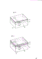
Figure 1A-1C is used for that monocrystalline method of the present invention is described and utilizes it to form the sectional drawing of model of the method for distribution.
Fig. 2 (a) and (b) and (c) be the vertical view that is used to illustrate the model of the monocrystalline Al crystal seed pattern that can adopt in the present invention.
Fig. 3 is the microscopical schematic diagram of explanation sweep type μ-RHEED.
Fig. 4 is explanation instantaneous heating (RTA) schematic representation of apparatus.
Fig. 5 (a) and (b) be the explanation specimen shape that can adopt among the present invention and the schematic diagram of laser light irradiation method.
Fig. 6 (a) and (b) be to be used for illustrating the specimen shape that can adopt among the present invention and the schematic diagram of laser light irradiation method.
Fig. 7 (a) and (b) be to be used for illustrating the specimen shape that the present invention can adopt and the schematic diagram of laser light irradiation method.
Fig. 8 is the schematic diagram that is used for illustrating the heating means of using the wire heater.
Fig. 9 is the schematic diagram that is used for illustrating the heating means of using lamp.
Figure 10 is the schematic diagram that is used for illustrating the heating means of using the high-frequency heating method.
Figure 11 is the schematic diagram that is used for illustrating the heating means of using electron beam.
Figure 12 is the schematic diagram that is used for illustrating the principle of sweep type μ-RHEED.
Figure 13 is the schematic diagram that is used for illustrating the fractographic principle of sweep type μ-RHEED.
Figure 14 A and B are the figure that shows electron diffraction pattern.
Shown in Figure 15-17 is an example of sweep type μ-RHEED image that demonstrates the crystal boundary of the Al film that deposits on the full surface of sample.Show respectively: before Figure 15-17A was the sample heating, Figure 15-17B was sample heating back (detecting diffraction spot 111), and Figure 15-17C is sample heating back (detecting diffraction spot 202).
Figure 18-the 19th carries out the oblique view of pattern of the sample of monocrystallineization.
The preferred embodiments of the present invention are, monocrystalline Al is connected with on-monocrystalline Al at least a portion, make on-monocrystalline Al monocrystallineization thereby resulting like this Al film is imposed heat treatment.
Another preferred embodiment of the present invention is, on-monocrystalline Al and at least one part of monocrystalline Al are joined, and resulting like this Al film carried out ion inject, and heat-treats then, makes on-monocrystalline Al monocrystallineization in this way.
At this moment, as the method that forms monocrystalline Al crystal seed, adopt with dimethyl alanate (Al(CH
3)
2H), monomethyl alanate (Al(CH
3) H
2), triisobutyl aluminium (Al(iC
4H
9)
3) be the CVD method of unstrpped gas on single crystalline Si depositing Al, form the Al monocrystal method ideal.
On the other hand, the method for formation on-monocrystalline body Al has:
Use above-mentioned gas, adopt the CVD method on the surface that constitutes by the material beyond the Al monocrystal depositing Al, form the multicrystal method of Al; Utilize sputter to form the multicrystal method of Al; Use trimethyl Al(Al(CH
3)
3) or diethyl aluminum chloride (Al(C
2H
5)
2Cl), adopt the CVD method to form the multicrystal method of Al, or the like.
Monocrystalline Al crystal seed can be according to fetching setting mutually with at least one part of on-monocrystalline Al that needs monocrystallineization.For example, crystal seed or dielectric film can form the clathrate figure, deposit crystal seed in the formed perforate position or also can make crystal seed and dielectric film form the lines figure alternate with the space on dielectric film.
The present invention also has a preferred embodiment to be, the Al monocrystal that forms in the aperture portion that forms on dielectric film is as crystal seed, on-monocrystalline Al heating with part beyond it, make it monocrystallineization, particularly, depositing Al and form the Al monocrystal in the perforate that is used to form electric contact optionally, depositing Al non-selectively on dielectric film then, then heat-treat, make the Al monocrystallineization on the dielectric film.Adopt such method, do not produce recess on the Al of tapping being positioned at, can form smooth Al film.
As the method that forms monocrystalline Al crystal seed, use the CVD method (below be referred to as the Al-CVD method) of alkyl aluminum hydride and hydrogen ideal.Utilize this CVD method, can be optionally provide depositing Al on the surface of Electronic Performance having resemble the single crystalline Si.
So-called alkyl aluminum hydride is dimethyl alanate (Al(CH
3)
2H) or monomethyl alanate (AlCH
3H
2).The method that formed on-monocrystalline Al before monocrystallineization is common sputtering method or CVD method.When adopting the CVD method, unstrpped gas has trimethyl aluminium (Al(CH
3)
3) or triisobutyl aluminium (Al(iC
4H
9)
3), diethyl aluminum chloride (Al(C
2H
5)
2Cl).Can form the good distribution that is suitable for semiconductor device with such method.
Be described in detail embodiments of the invention with reference to the accompanying drawings.
Fig. 1 is the sectional drawing that monocrystalline method of the present invention is used to form the pattern of distribution in order to explanation.
Among Fig. 1, the 1st, the matrix that constitutes by single crystalline Si etc., the 2nd, the dielectric film that constitutes by silicon dioxide etc., the 3rd, monocrystalline Al crystal seed, the 4th, utilize hereinafter described monocrystalline method to be transformed into the Al of monocrystal.
At first, on matrix 1, form dielectric film 2.
Then, utilize the reactive ion corrosion to form perforate, come out in the part surface of matrix 1.Dielectric film described here is silicon dioxide film or silicon nitride film or the oxidized silicon nitride film etc. of NSG, PSG, BSG, BPSG etc.The thermal oxidation method that the employing people know, CVD method, sputtering method etc. can form these films.
Then, in perforate, form monocrystalline Al3(the one Al film).In this case, utilize above-mentioned Al-CVD method can fill part and optionally in perforate, form the Al monocrystal.At this moment matrix surface temperature more than the decomposition temperature of alkyl aluminum oxide~below 450 ℃, more than 260 ℃, 440 ℃ with next better, preferably more than 270 ℃, below 350 ℃.
Formed like this Al monocrystal, not only good with the interface of Si substrate, and also surface property is good.
After in perforate, forming Al monocrystal 3, at monocrystalline Al3 and formation on-monocrystalline Al4(the 2nd Al film above the dielectric film 2).Can use the known deposition process except that above-mentioned Al-CVD method this moment.In addition, under the situation of using the Al-CVD method, also can provide ion or electronics to not having dielectric film 2 surfaces of supplying with Electronic Performance, perhaps adopt surface modification technologies such as ion dam age or ion injection to make it substantially have the electron donability energy with plasma.If such introducing surface modification operation also can form on-monocrystalline Al(Fig. 1 (a) so on dielectric film 2).
Then, carry out heat treatment hereinafter described, can make on-monocrystalline Al monocrystallineization.At this moment heat treatment can be carried out, and also can form dielectric film 5 afterwards and carry out afterwards.
In addition, heat treatment also can be carried out after the on-monocrystalline Al that will need monocrystallineization forms pattern by desired distribution shape, perhaps also can form pattern again after monocrystallineization.
Shown in Fig. 1 (b), after with the Al4 patterning, formed dielectric film 5.This layer dielectric film 5 can similarly adopt CVD method or sputtering method to wait with dielectric film 2 and form.
By the above, can form monocrystalline Al distribution.
If form multilayer wiredly, repeat this technical process and can obtain two layers of Al monocrystalline distribution structure shown in Fig. 1 (c).Repeat this technical process further, also can obtain multi-layer wiring structures such as three layers, four layers.
In Fig. 1 (c), the 5th, interlayer dielectric, the 6th, the monocrystalline Al of selective deposition, the 7th, the Al of monocrystallineization, the 8th, protection dielectric film.
Above-describedly be, the metal that with Al is Main Ingredients and Appearance is the situation of pure Al, in addition can also make to contain micro-Si(for example about 1%) Al(be Al-Si) monocrystallineization.When using above-mentioned Al-CVD method in this case, if import SiH with alkyl aluminum hydride gas and hydrogen
4, Si
2H
6Deng the gas that contains the Si compound, carry out film forming, just can form Al-Si monocrystal crystal seed.
The profile instance of the Al of monocrystalline shown in Fig. 2 crystal seed.Fig. 2 (a) is that to be the clathrate pattern setting length of side on the insulator 11 that semiconductor substrate for example forms on the surface of Si be L
1Peristome, the example of deposition monocrystalline Al in peristome optionally.The not shown on-monocrystalline Al that covers monocrystalline Al in insulator 11 and the peristome 12 and form is a crystal seed with monocrystalline Al, makes on-monocrystalline Al be transformed into monocrystal by heating.Fig. 2 (b) is depicted as the example that forms aperture pattern, and the length of side of aperture portion is L
2, spacing is L
3Fig. 2 (c) is depicted as width L
5Insulator 11 and width L
4Peristome 12 form the example of the stripeds pattern alternate with the space.No matter being any situation, all is optionally to deposit monocrystalline Al in peristome, and not shown on-monocrystalline Al covers monocrystalline Al and forms above the insulator.With monocrystalline Al is crystal seed, makes on-monocrystalline Al film monocrystallineization by heating.
Narration makes the heat treatment method of Al or Al-Si monocrystallineization below.
Basic operation is as described below.The sample that making has the section as Fig. 1 (a) and (b) heats.Before heating and afterwards, carry out that X-ray diffraction, traditional RHEED are observed, sweep type μ-RHEED microscopic examination.
By make at sedimentation state as heat is multicrystal the 2nd Al film monocrystallineization, can think, this be since the Al atom become be easy to flow, due to atom rearranges.In the past, people knew that the semiconductor with covalent bonds such as Si, GaAs on insulator film is monocrystallineization by heat treatment.People also know, Al on insulator film or Al-Si film are the polycrystal that the crystal grain of several μ m is formed through form by crystal grain diameter in about 400 ℃ of heat treatments, but the present invention has disclosed, if there is monocrystalline Al zone in the lower floor at Al or Al-Si, so more than spreading all over 10 μ m the size scope in, Al on the insulator or Al-Si also can monocrystallineization.
As the heating means of sample, utilize electric furnace at H except routine
2, N
2, Ar or these gases mixed atmosphere in heat treated and in a vacuum outside the heating, also can adopt instantaneous heating furnace (hereinafter to be referred as RTA) heating, LASER HEATING, with methods such as wire heater heats such as carbon heater, high-frequency heating, lamp heating, electron beam heating.
Usually, in large scale integrated circuit, formed pure Al or Al-Si film above the Si since heating and with Si reaction, etch Si matrix for example, the perhaps Si that forms in the lower floor of Al or the Al-Si leakage that produces the P-n knot.Therefore, wish that heat treated only carries out under low temperature.But in order to make Al or Al-Si monocrystallineization by heating, the atom of Al must reach because heat energy and mobile degree.As heating means, wish only to heat Al or Al-Si and do not heat the Si matrix of Al or Al-Si lower floor.
Heating can utilize the heater that is located at the matrix back side to carry out in sweep type μ-RHEED microscope of Fig. 3 in the vacuum.
During heat treatment,, wish under high vacuum, to carry out preferably about 1 * 10 in a vacuum in order to suppress the Al surface oxidation
-6The high vacuum that torr is following.Among Fig. 3, the 20th, electron gun, the 21st, electron beam, the 22nd, diffraction electronics line, the 23rd, fluorescent plate, 24,24 ' and 24 " be optical fiber; 25,25 ' and 25 " be photomultiplier, 26,26 ' and 26 " be the diffraction spot strength signal that is transformed into the signal of telecommunication, the 27th, sweep signal; the 28th, CRT; the 29th, secondary electron signal, the 30th, secondary electron detector, the 31st, sample; the 34th, vacuum chamber, the 35th, exhaust apparatus.
With the vacuum chamber of packing into of the sample shown in Fig. 1 (a), with the back side heating of heater 32 from sample 31.Measure the temperature of sample from the back side of sample 31 with thermocouple 33.Heating means can also adopt lamp heating, LASER HEATING except that heater heats.With exhaust apparatus 35 vacuum chamber 34 is vacuumized.The vacuum degree of sample heating chamber, initial vacuum 34 is about 5 * 10
-4Torr, the vacuum degree in the heating process is about 5 * 10
-9-5 * 10
-8Torr.Though wish that vacuum degree is higher, though poorer than above-mentioned vacuum degree, also can monocrystallineization by heat treatment.
The temperature of measuring with thermocouple 32 about more than 550 ℃ the time, the Al monocrystallineization.
The following describes and be applicable to instantaneous heating furnace of the present invention (hereinafter to be referred as RTA).
Use a RTA heating sheet surface at short notice, thereby the reaction of Al or Al-Si and Si substrate is reduced.
The structure example of RTA device has been shown among Fig. 4.
Wherein 200 is matrixes, the 201st, and the substrate support platform.The substrate support platform is made by quartz, is loaded with matrix 200 on the ratchet shown in Fig. 4 205.The 202nd, quartz ampoule, its section are rectangles or circular for well.The quartzy window of making can be installed on stainless metal in addition.The 203rd, lamp is made into wire.The light that is sent by lamp 203 reflects through reflecting plate 204, shines on the matrix 200.The Al depositional plane of matrix 200 is towards a side of lamp.Lamp can use iodine-tungsten lamp, tungsten lamp, Xe lamp, Xe-Hg lamp.In the RTA device, use the fast iodine-tungsten lamp of firing rate.
Pressure during heating in the crystal reaction tube can be in decompression down also can be under atmospheric pressure.Can use H as gas atmosphere
2, Ar, N
2Or their mist.
Owing to may obtain the minimum high-purity hydrogens of impurity such as water content, oxygen, therefore preferably use H
2Atmosphere.
In the RTA of said structure device, if heat under the temperature more than 550 ℃ about, Al will monocrystallineization.Be warming up to heat treatment temperature by room temperature and roughly need 5-30 second.Heat treatment time is approximately 10 seconds to 1 minute.In above-mentioned heating-up time and heat treatment time scope, the scope of monocrystallineization does not have difference.
In order to realize monocrystallineization, heating-up temperature must be about more than 550 ℃.In addition, substrate temperature is to use the radiation thermometer of application PbS to be measured by matrix surface.
The following describes and can be used for LASER HEATING of the present invention.
Utilize LASER HEATING also can only heat matrix surface, in addition, also have the monocrystalline scope characteristics wideer than RTA device.
As laser, can use power output is argon ion laser (hereinafter to be referred as the Ar laser) about several W to 20W, krypton ion laser (hereinafter to be referred as the Kr laser), He-Ne laser, CO
2Laser, YAG laser, excimer laser such as ArF or KrF or XeF or XeCl.Frequency of oscillation can be continuous oscillation, also can be the impulse hunting of about 10-100Hz.
Characteristics with LASER HEATING are, can laser scannings on sample, enlarge the zone of monocrystallineization.Just utilizing laser scanning to enlarge the monocrystalline zone below is illustrated.
The sample that uses is, at Fig. 5 (a) or (b), Fig. 6 (a) or (b) or Fig. 7 (a) or (b) shown in semiconductor substrate 61 on form an Al film 62, its width is L
10, on the full surface of matrix, form the 2nd Al film 63 again.Shown in Fig. 5 (b) or Fig. 6 (b), also can on second portion aluminium 63, form dielectric film 65 comprehensively.Perhaps also can be such by Fig. 7 (a) and (b), form and the vertical substantially dielectric film that is linear 66 of the lines of an Al film 62.
Press shown in the line 68 among Fig. 5 (a) and (b) or Fig. 7 (a) like that, scanning laser beam 67 repeatedly on said sample perhaps press shown in the middle arrow 69 of Fig. 6 (a) and (b) or Fig. 7 (b) along a scanning direction.The laser beam of Fig. 5 (a) and (b) or Fig. 7 (a) becomes about 20-100 μ m with the Ar laser of continuous oscillation or the XeCl excimer laser focusing of impulse hunting.
Under the situation shown in Fig. 6 (a) and (b) or Fig. 7 (b), for example,, make the conglobate laser beam of focusing become collimated light beam 71 by the optical system 70 of using cylindrical lens.
As Fig. 5 (a) or (b), Fig. 6 (a) or (b) or Fig. 7 (a) or (b) shown in, the lines of the scanning direction of laser beam or collimated laser beam and the first aluminium film roughly meet at right angles.
On the Si substrate, form about 7000
 Thermal oxidation SiO
2, at the wide 10 μ m that approximate of the first aluminium film, 62 lines, the thickness of the
Thermal oxidation SiO
2, at the wide 10 μ m that approximate of the first aluminium film, 62 lines, the thickness of the second aluminium film 63 about 5000
The sample shown in Fig. 6 (a) on, make Ar laser become collimated light beam 71, along the velocity scanning sample of a direction (69) with about 1 cel.Does not heat at the sample back side.
The power output of Ar laser is about 20-50W, and the laser energy density on the sample back side is about 50-200KW/cm
2The atmosphere of LASER HEATING is H
2Atmosphere, pressure are 1 atmospheric pressure.
Measure the temperature at laser radiation position by means of the radiation thermometer that uses the PbS detector, thereby determine substrate temperature.Roughly more than 500 ℃ the time, the Al on first dielectric film can monocrystallineization for substrate temperature.
The following describes by going for the method that wire heater of the present invention heats.
Fig. 8 is the figure that adopts the heating means of wire heater in order to explanation.To add hot basal body 82 places on the heating substrate support platform 81.Heating supporting station 81 is made by carbon.Above adding hot basal body 82, wire heater 83 is set.This wire heater 83 also is to be made by carbon, by power supply 84 making current.Heating supporting station 81 also is to utilize the heater (not shown) that is installed in the heating supporting station back side to heat.In addition, wire heater 83 moves along the direction of arrow 85.
The pressure of heating atmosphere is not limit, and is pressed onto vacuum from atmosphere and all can.In order to prevent the oxidation on Al surface, preferably adopt H
2, N
2, Ar or their mixed atmosphere.Though also can monocrystallineization under vacuum, under atmospheric pressure Zhuan Zhi structure can be simplified.
Part under the wire heater, the second aluminium film monocrystallineization.Utilize such wire heater heats, be positioned at substrate temperature under the wire heater roughly more than 550 ℃ the time, the second aluminium film monocrystallineization.Substrate temperature is measured by means of the radiation thermometer that uses PbS.
Adopt the characteristics of the mode of heating of wire heater to be, laser is the same with using, and can scan heating region, enlarges the monocrystalline scope.
The following describes and can be used for the method for utilizing the lamp heating of the present invention.
Fig. 9 is the figure that uses the lamp heating means in order to explanation.On heating substrate support platform 91, be placed with and add hot basal body 92.Heating supporting station 91 is made by carbon.Lamp 93 can be mercury vapor lamp, Hg-Xe lamp, Xe lamp, Xe photoflash lamp or the like.Preferably lamp is made linear structure.The light that is sent by lamp 93 focuses on matrix surface by means of speculum 94 and becomes wire.The heater (not shown) that utilization is located at the heating supporting station back side will heat supporting station 91 heating.By portable lamp the thermal treatment zone 95 is moved adding on the hot basal body along the direction of arrow 96 in addition.The pressure of heating atmosphere is not limit, and all can from atmospheric pressure to vacuum.In order to prevent the Al surface oxidation, preferably use H
2, N
2, Ar or their mixed atmosphere.Also can monocrystallineization under vacuum, but under atmospheric pressure the structure of device can be simplified.
The monocrystallineization of the 2nd Al film occurs in and is in the wire area heated, and in heating region 95, substrate temperature is about more than 550 ℃ the time, the 2nd Al film monocrystallineization.Substrate temperature is measured by means of the radiation thermometer that uses PbS.
The following describes and can be used for high-frequency heating method of the present invention.
Figure 10 is the figure that uses the heating means of high-frequency heating in order to explanation.On heating substrate support platform, be placed with and add hot basal body 103.The 101st, the supporting station of making by carbon.The 102nd, reserve the plate of the quartz system that certain intervals is provided with.As shown in figure 10, utilize the heating supporting station that is loaded with matrix around the high frequency coil (not shown) heating that is provided with.Because quartz plate 102 can not be used high-frequency heating, thereby the some 104 of matrix is heated to the highest temperature.
Thin slice is moved along direction shown in the arrow 105, and also move on wafer in the zone 104 that then is heated to high temperature.The pressure of heating atmosphere is not limit, and all can from atmospheric pressure to vacuum.In order to prevent Al surface oxidation, the most handy H
2, N
2, Ar or their mixed-gas atmosphere.Also can monocrystallineization under vacuum, but under atmospheric pressure the structure of device can be simplified.In following embodiment, atmosphere pressures all is an atmospheric pressure.
The monocrystallineization of the second aluminium film occur in be wire be heated the zone 104 in, when the substrate temperature of the thermal treatment zone 104 is about more than 550 ℃, the second aluminium film monocrystallineization.Substrate temperature is measured by means of the radiation thermometer that uses PbS.
The following describes the heating means that can be used for use electron beam of the present invention.
Figure 11 is the heating means figure that electron beam is used in explanation.From the electron beam 113 of filament 112 by focusing coil 115, scanning coil, deflecting plate 115 ' be focused into wire adding on the hot basal body 111.114 parts on the matrix are heated to high temperature by wire.Because matrix moves along direction shown in the arrow 116, also move on matrix in the zone 114 that is heated to high temperature.
In order to prevent the aluminium surface oxidation, wish that heating atmosphere pressure is high vacuum.About 10
-6Carry out the aluminium monocrystallineization under the vacuum degree below the torr.The translational speed of matrix is about 0.5-10cm/ branch.The matrix surface temperature of the thermal treatment zone is about (measures) that aluminium can monocrystallineization more than 450 ℃ the time with the radiation thermometer that uses PbS.
Explanation about the Observations Means that utilizes the microscopical crystal region of sweep type μ-RHEED shown in Figure 3.
Sweep type μ-RHEED microscope be Extended Abstracts Of the 21th Conference on Solid StateDevices and Materials (1989) P.217 with Japanese Journal of Applied Physics vol.28.No.11(1989) disclosed means among the L2075.The RHEED(reflection high energy electron diffraction in past, reflection high-velocity electrons diffraction) method is that electron beam is injected the test portion surface with 2-3 ° low-angle, the diffraction pattern that is produced by the diffraction electron beam is estimated the crystallinity on test portion surface.But,, can only obtain the average information on test portion surface because beam diameter competes to reach 100 μ m to hundreds of μ m.In sweep type μ-RHEED microscope shown in Figure 3, be contracted to 0.1 μ m from the beam diameter of electron gun 20, on phosphor screen 23, can observe electronogram from the specific tiny area in test portion surface.And electron beam 21 is carried out two-dimensional scan on the test portion surface, diffraction electron ray 22 is directed to phosphor screen 23, with any diffraction spot Strength Changes on the diffraction pattern as picture intelligence 26,26 ' and 26 ", on CRT28, can access two-dimensional image (scanning μ-RHEED image) according to the test portion surface of diffraction spot Strength Changes.At this moment, as Figure 12, if observe scanning μ-RHEED image with the different diffraction spot A on the diffraction pattern and C, the lip-deep parallel lattice plane of test portion then, for example, though all be (100) face, can image conversion owing to distinguish out the crystal boundary face that in face, rotates.Therefore, diffraction spot A be the face that produces diffraction pattern with the vertical intersection (line 1) on the plane of incident beam foundation on diffraction spot, diffraction spot C is the diffraction spot on not online 1.As Figure 13, the parallel lattice plane on the specimen surface for example is (100) face, and under the situation that crystal grain X and Y rotate in face mutually, crystal grain X and Y together are represented as the high zone of intensity in scanning μ-RHEED image of diffraction spot A.And in scanning μ-RHEED image, have only crystal grain X to be expressed out as the high zone of intensity with diffraction spot C.Thereby as observe using the diffraction spot A that resembles as shown in Figure 12 and scanning μ-RHEED image of C, the crystal that then can identify observed zone contains the polycrystal or the monocrystal of rotation in the face.
The following describes and utilize heat treatment to make SiO
2On the example of aluminium monocrystallineization.
Explanation about sample.
Monocrystal crystal seed figure is the figure that resembles above-mentioned Fig. 2.Promptly under the situation that resembles the graticule Fig. 2 (a), L
1Size be 0.5 μ m to 20 μ m, under the situation that resembles the perforate figure Fig. 2 (b), L
3Be below the 20 μ m, resemble Fig. 2 (c) lines and at interval under the situation of figure, L
5Be below the 20 μ m.On such monocrystal crystal seed figure, form on-monocrystalline aluminium then, with the gained sample as sample.
When estimating this sample, only observe the peak value of aluminium (111) face with X-ray diffraction method.With beam diameter is the RHEED device in the past of 100 μ m to 1mm when observing electronogram, observes the ring-type figure shown in Figure 14 (a).Thereby the aluminium of knowing comprehensive deposition is the polycrystal of (111) orientation.
, in above-mentioned X-ray diffraction and the observation of RHEED in the past,, do not know the size of crystal grain though be confirmed to be polycrystal.In sweep type μ-RHEED microscope, use the occasion of the electron beam observation electronogram that is contracted to 0.1 μ m, though weak strength is observed the point-like figure resembling shown in Figure 14 (b).Figure 15 (a) utilizes the diffraction spot intensity on the point-like diffraction pattern to observe the result who scans μ-RHEED image.Oblique line partly is the high zone of diffraction spot intensity, and blank parts is the low zone of diffraction spot intensity.
Know that by oblique line subregion size grain size is approximate number μ m to 10 a μ m level.
Same sample after 15 minutes, is observed electronogram and scanning μ-RHEED image in 550 ℃ of heating in sweep type μ-RHEED microscope.On electronogram, observe than intensity before the heating also eager to excel in whatever one does resemble speckle pattern Figure 14 (b).The diffraction pattern of Figure 14 (b) can be known the diffraction pattern that this forms when direction makes electron beam incident from (101) of aluminium (111) face according to the position that diffraction spot occurs.Figure 15 (b) and (c) be the diffraction spot A(111 diffraction spot that utilizes on the diffraction pattern of Figure 14 (b)) and diffraction spot C(202 diffraction spot) intensity observe the result of scanning μ-RHEED image.No matter diffraction spot A and C are strong on which position, test portion surface, thereby confirm viewing area monocrystallineization fully.That is to say, even SiO
2On the aluminium film, when having aluminum single crystal in the aluminium lower floor, utilize heat treatment can make it monocrystallineization.Only observe Al(111 when estimating sample after the heat treatment with the X-ray diffraction device) peak value of face, when observing electronogram with RHEED device in the past again, shown in Figure 14 (b), observe the speckle pattern of expression monocrystal.
Then use other sample observation monocrystallineization.This sample is as shown in Figure 16 (a), utilizes thermal oxidation method to form the thick silicon oxide film of 1 μ m on the Si matrix, on this silicon oxide film, and the opening (silicon opening portion) that utilizes dry ecthing to leave silicon face is exposed.
Forming as Fig. 2 (a) and (b) in the zone of Figure 16 (a) (I) and such grid figure (c), perforate figure or lines and interval figure.Zone (II) is the zone that does not form above-mentioned grid figure, opening figure or lines and interval figure, promptly is SiO fully
2The zone.Such shown in Figure 16 (a), at SiO
2Form on the matrix of figure, by using DMAH and H
2The CVD method at first only optionally deposit first's aluminium at the Si opening portion, after surface modification, deposition second layer aluminium on the whole substrate face.
After the deposition of aluminum, only observe Al(111 when evaluating with x-ray method) peak value of face.Be the former RHEED device of 100 μ m-1mm when observing electron diffraction diagram with beam diameter again, observe ring-type figure such shown in Figure 14 (a).Thereby the aluminium of confirming full surface deposition is the polycrystal of (111) planar orientation.Electron beam with reduced to 0.1 μ m is observed electronogram in sweep type μ-RHEED microscope then, although weak strength observes such speckle pattern shown in Figure 14 (b).Utilize the diffraction spot intensity on the mottled diffraction pattern to observe scanning μ-RHEED image, the result is as Figure 15 (a), the polycrystal of being made up of the crystal grain of several μ m to 10 μ m.
This sample after 15 minutes, is observed electronogram and scanning μ-RHEED image 645 ℃ of heating in scanning μ-RHEED microscope.Observe the intensity speckle pattern stronger, resemble Figure 14 (b) shown in of electronogram before than heating.In the diffraction pattern of Figure 14 (b), from position that diffraction spot occurs as can be known, it is from Al(111) diffraction pattern that generates during (101) direction incident beam on the face.Figure 16 (b) and (c) be the diffraction spot A(111 diffraction spot that utilizes on the diffraction pattern of Figure 14 (b)) and diffraction spot C(202 diffraction spot) intensity observe the result of scanning μ-RHEED image.At Figure 16 (b) with (c), oblique line partly is the high zone of diffraction spot intensity.Figure 16 (b) and (c) in all high zone of intensity be (111) monocrystal.By Figure 16 (b) and (c) as can be known, the monocrystallineization zone is about 10 μ m apart from the zone (I) that forms the Si opening portion.That is to say,,, form zone (I) 10 μ m with interior part monocrystallineization at the distance figure even do not expose the part of Si on the Al lower floor position by heat treatment.
The figure that forms in the zone (I), no matter be the grid figure of Fig. 2 (a), perforate figure and the lines (c) and which kind of situation in the space diagram of (b), apart from zone (I) but monocrystallineization all within the scope of about 10 μ m.
SiO
2Thickness is 500
 During-1 μ m, no matter SiO
2How much thickness is, because the regional extent of heat treatment and monocrystallineization is identical with Figure 16 (b) and (c).Even at SiO
2Going up comprehensively, the aluminium thickness of deposition is 500
During-1 μ m, no matter SiO
2How much thickness is, because the regional extent of heat treatment and monocrystallineization is identical with Figure 16 (b) and (c).Even at SiO
2Going up comprehensively, the aluminium thickness of deposition is 500
 -1 μ m, the monocrystalline zone also with Figure 16 (b) and (c) identical.
Monocrystalline zone when utilizing LASER HEATING, wire heater heats, high-frequency heating and electron beam heating etc. to make the heating means that heating region moves on matrix is according to following such mensuration.
In the zone of Figure 17 (a) (III), form the grid figure identical, opening figure, lines and interval figure, in the zone of Figure 17 (a) (IV), form first dielectric film with the zone (I) of Figure 16 (a).On matrix like this, form the 1st aluminium and the 2nd aluminium.
The 2nd aluminium that is under the sedimentation state is the polycrystal that crystal grain diameter is counted μ m to 10 μ m.
With laser beam shown in Figure 5 directions X scanning along Figure 17 (a).And when the flat shape parallel laser of use, the directions X of the thermal treatment zone when lamp heating, radio frequency (RF) heating and electron beam heat moved resemble Fig. 6.
After the heat treated with the fractographic Figure 17 (b) and (c) of the results are shown in of scanning μ-RHEED.Observe the electronogram that produces by sweep type μ-RHEED microscope and be than the intensity before the heating and also be eager to excel, the spot figure resembling shown in Figure 14 (b).Utilize the diffraction spot A(111 diffraction spot on the diffraction pattern of Figure 14 (b)) and diffraction spot C(202 diffraction spot) intensity when observing scanning μ-RHEED image, observe Figure 17 (b) for example and (c) shown in scanning μ-RHEED image.Oblique line is partly represented the zone that diffraction spot intensity is high.Diffraction spot A and the strong zone of C both are (111) monocrystal zones.
In Figure 17 (c), if measure L
8Distance, then know because heat treatment and the area size of monocrystallineization.
Moreover, concerning Figure 17 (a), on the figure of Figure 17 (b) and the dielectric film that (c) forms on the same area, in the zone of said sample (III), only there is one article of the 1st aluminium.And the moving direction of heating region is the directions X of Figure 17 (a).In Figure 17 (c), L
8About 10 μ m shown in being, but in the sample that carries out laser annealing, wire heater heats, lamp heating, radio frequency heating and electron beam heating L
8Reach about 1cm.
That is, confirm,,, form the about 1cm in zone with interior part monocrystallineization at the distance figure even on aluminium lower floor position, do not expose the part of Si by heat treatment.
For the SiO of monocrystallineization
2On Al measure its anti-electron transfer.Al or the Al-Si distribution that produces with sputtering method in the past is at 250 ℃, 1 * 10
6A/cm
2Energizing test under, the distribution sectional area is 1 μ m
2The time obtain 1 * 10
2-10
3The average distribution life-span about hour.In contrast to this, in above-mentioned test, sectional area is 1 μ m according to monocrystal Al distribution of the present invention
2Distribution obtain 10
4-10
5Hour the distribution life-span.In addition, even the distribution of wide 0.8 μ m, thick 0.3 μ m also obtains 10 under above-mentioned test
3-10
4Hour the average distribution life-span.
Also having, the Al of monocrystallineization is processed into wide about 1 μ m, utilize the plasma CVD method silicon nitride film, is under 150 ℃ at atmosphere temperature, applies 1000 hours stress, measures the ratio that broken string produces.In the long distribution of 1mm, the Al that sputtering method in the past produces, the outage of 1000 lines is 10-20%, in contrast to this, according to Al of the present invention, does not produce broken string in 1000 lines.
That is to say, can obviously improve anti-EM and SM by monocrystalline Al distribution.
The example that other more suitably implement state of the present invention is as crystal seed, with the on-monocrystalline Al heating of in addition part and monocrystallineization with the monocrystalline Al that forms in the opening portion that forms on dielectric film.Especially selectively deposition of aluminum and after forming aluminum single crystal, also non-selectively deposition of aluminum on dielectric film in perforate.And preferably after injecting ion, apply heat treatment and make aluminium monocrystallineization on the dielectric film.Resemble this means as utilization and can not form recess in the aluminium place in perforate, obtain smooth aluminium film.
On-monocrystalline aluminium film utilizes heating after amorphization or controlled micro crystallization, with aluminum single crystal as crystal seed and monocrystallineization.
In the present invention, use in the formed on-monocrystalline aluminium film known ion implantation to inject H above-mentioned resembling
+(proton), Ar
+, Si
+And Al
+Plasma.As ionic species, also be fine though inject above-mentioned ion in addition, in order not damage the reliability of very lagre scale integrated circuit (VLSIC), wish to use above-mentioned four kinds of ions, and in above-mentioned four kinds of ions, preferably can use Al with Al or Al-Si distribution
+Or H
+
As ion implanting conditions, can the above accelerating voltage, 1 * 10 of about 50KV
15Cm
-2Above dosage is thrown above-mentioned H into
+, Al
+, Ar
+And Si
+Ion.Consequently, even the thickness of the 2nd aluminium is about 5000
 Also can make second aluminium amorphous material or the controlled micro crystallization.
By injecting ion, be multicrystal aluminium amorphous materialization at sedimentation state.Because the multicrystal aluminium atom of amorphous al atomic ratio flows easily by heat energy, therefore, the heat treatment phase ratio such with polycrystal can monocrystallineization under lower temperature.In the past, the semiconductor with covalent bonds such as Si and GaAs on insulator film utilizes heat treatment and monocrystallineization is known.For example, in being called the means of phase epitaxy method (hereinafter to be referred as SPE), depositing silicon on monocrystalline silicon piece carries out that ion injects and the amorphized silicon attitudeization that makes deposition, heat-treats in electric furnace etc. then, makes the silicon single crystalization of amorphous material.The present invention finds, even metallic film, aluminium carrying out ion to inject on the dielectric film of noncrystallineization or controlled micro crystallization gets final product monocrystallineization at a lower temperature, past, Al on the insulator film or Al-Si film grow up to the polycrystal of grain size number micron degree by about 450 ℃ heat treatment.But owing in the such structure of Fig. 1 (a), do not determine the gimmick of deposition of aluminum, selectively Chen Ji aluminium (the 1st aluminium of Fig. 1 (a)) is not aluminum single crystal, the monocrystallineization so can not utilize heat treatment.According to the present invention,, then after ion injects, utilize the heat treatment can monocrystallineization even the aluminium film (the 2nd aluminium of Fig. 1 (a)) on insulator film during beginning is selected growth aluminum single crystal (the 1st aluminium of Fig. 1 (a)) if exist in underclad portion.
Semiconductor substrate is silicon chip preferably, but semiconductor chips such as GaAs, InP beyond the Si, Ge also are fine.The section structure of the sample of formation Al or Al-Si is shown in Fig. 1 (a).
In the embodiment of the following stated, second aluminium is thinner or thicker on first aluminium, does not have what difference when monocrystalline.Have again, shown in Fig. 1 (b), also do not have what difference even on the 2nd aluminium film, form dielectric film 5.Dielectric film can use the SiO that is produced by the atmospheric pressure cvd method
2, phosphorus doping oxide-film (PSG), boron doped oxide film (BSG), phosphorus and boron doped oxide film (BPSG), the silicon nitride film (SIN) that produces by the decompression method, the silicon nitride film that produces by the ECR method.
The heat treatment method that carries out for monocrystallineization as previously mentioned.
The following describes the example of the aluminium monocrystallineization that comprises noncrystalline and even controlled micro crystallization operation.
Explanation about test portion.
Monocrystal crystal seed figure is the figure that resembles above-mentioned the 2nd figure.Promptly under the situation that resembles the grid figure Fig. 2 (a), L
1Size be 0.5 μ m to 20 μ m, under the situation that resembles the perforate figure Fig. 2 (b), L
3Be below the 20 μ m, resemble Fig. 2 (c) lines and at interval under the situation of figure, L
5Be below the 20 μ m.Form on-monocrystalline aluminium on single crystal seed figure like this, the gained sample is as sample.
When estimating this test portion, only observe Al(111 with X-ray diffraction method) peak value of face.When observing electronogram with the RHEED device in the past of beam diameter 100 μ m to 1mm again, observe the ring-type figure shown in Figure 14 (a).Hence one can see that, and the aluminium of deposition is the polycrystal of (111) planar orientation comprehensively.
But, observe by above-mentioned X-ray diffraction and RHEED in the past, though be confirmed to be polycrystal, do not know grain size.When in sweep type μ-RHEED microscope, observing electronogram, though weak strength is observed the diffraction spot resembling shown in Figure 14 (b) with the electron beam of reduced to 0.1 μ m.Figure 15 (a) is to use the diffraction spot intensity on the mottled diffraction pattern to observe the result of scanning μ-RHEED image.Oblique line partly is the high zone of diffraction spot intensity, and blank parts is the low zone of diffraction spot intensity.
Know that by the size of oblique line subregion grain size is approximate number μ m-10 μ m.
On this sample under the 50KV accelerating voltage with 1 * 10
16/ cm
2Dosage will be for example Al
+Ion injects wherein.
One injects above-mentioned ion, and the 2nd aluminium is with regard to amorphous materialization or controlled micro crystallization.Resemble and confirmed amorphous materialization and controlled micro crystallization following.At first, carrying out X-ray diffraction measures.Under sedimentation state, can observe Al(111) diffraction peak, but do not observe diffraction peak when measure injecting the X-ray diffraction figure of sample of ion about aluminium.In addition, if utilize RHEED device in the past to measure electronogram, when measuring the ring-type figure, observe neither the ring-type figure is not again a speckle pattern, but so-called haloing electronogram.Promptly by injecting ion, Al or Al-Si film neither monocrystal be not polycrystal again, and become noncrystalline or microcrystalline state.
In sweep type μ-RHEED microscope, same sample after 15 minutes, is observed electronogram and scanning μ-RHEED image 250 ℃ of heating.In electronogram, observe than intensity before the heating strong resemble speckle pattern Figure 14 (b).The position that diffraction spot from the diffraction pattern of Figure 14 (b) occurs as can be known, the diffraction pattern that this produces when being (101) direction incident from Al (111) face of electron beam.Utilize the diffraction spot A(111 diffraction spot on the diffraction pattern of Figure 14 (b)) and diffraction spot C(202 diffraction spot) the intensity result that observes scanning μ-RHEED image be Figure 15 (b) and (c).On any position of specimen surface, diffraction spot A and C are strong simultaneously, and observing the district becomes monocrystal fully.That is to say, even SiO
2On the aluminium film, as long as have aluminum single crystal in the aluminium lower floor, but then utilize just monocrystallineization of heat treatment.When with the test portion after the X-ray diffraction device evaluation heat treatment, only observe the peak value of (111) face of Al, when observing electronogram with RHEED device in the past again, observe the monocrystalline speckle pattern resembling shown in Figure 14 (b).
Then use other sample observation monocrystallineization.This sample is as shown in Figure 16 (a), utilizes thermal oxidation method to form the thick silicon oxide film of 1 μ m on the Si matrix, utilizes dry ecthing to leave on this silicon oxide film to manifest the opening (silicon opening portion) on Si surface.
In the zone of Figure 16 (a) (I), form resemble Fig. 2 (a) and (b) and (c) shown in grid figure, perforate figure or lines and figure at interval.Zone (II) is the zone that does not form above-mentioned grid figure, perforate figure or lines and interval figure, promptly whole SiO
2The zone.Shown in Figure 16 (a), forming SiO
2With the CVD method of using DMAH and hydrogen at first, only selectively deposit the 1st aluminium on the matrix of pattern at the Si opening portion, after the surface modification operation, deposition the 2nd aluminium on whole substrate.
After the deposition of aluminum, when estimating, only observe the peak value of (111) face of Al with X-ray diffraction method.In addition, when the RHEED device in the past that with beam diameter is 100 μ m-1mm is observed electronogram, observe the ring-type figure resembling shown in Figure 14 (a).Thereby think that the aluminium of comprehensive deposition is the polycrystal of (111) planar orientation.Then, when in sweep type μ-RHEED microscope, using the electron beam that is contracted to 0.1 μ m to observe electronogram, although weak strength is observed the speckle pattern resembling shown in Figure 14 (b).Utilize the diffraction spot intensity on the mottled diffraction pattern to observe scanning μ-RHEED image, as Figure 15 (a), the polycrystal of forming by the crystal grain of several μ m-10 μ m.This polycrystalline aluminium injects and noncrystallineization by ion.
This sample after 15 minutes, is observed electronogram and scanning μ-RHEED image in 260 ℃ of heating in scanning μ-RHEED microscope.Electronogram is observed the speckle pattern resembling shown in Figure 14 (b) than the preceding intensity height of heating.In the diffraction pattern of Figure 14 (b), the position that occurs by diffraction spot as can be known, the diffraction pattern that generates during this (101) direction incident beam from Al (111) face.Utilize the diffraction spot A(111 diffraction spot on the diffraction pattern of Figure 14 (b)) and diffraction spot C(202 diffraction spot) intensity observe scanning μ-RHEED image, Figure 16 (b) and (c) consequently.Figure 16 (b) and (c) bend partly be the high zone of diffraction spot intensity.Figure 16 (b) and (c) in all high zone of intensity be (111) monocrystal.Learn that by Figure 16 (b) with (c) it is about 10 μ m that the monocrystalline zone forms zone (I) apart from the Si opening portion.That is to say, confirmed already,,, form the interior own monocrystallineization of part of the about 10 μ m distance in zone (I) apart from figure even on aluminium lower floor position, do not manifest the part of Si by heat treatment.
The figure that forms in zone (I) is no matter be the perforate figure of grid figure, (b) of Fig. 2 (a) and lines (c) and any in the figure at interval, in monocrystallineization all in the scope of regional (I) about 10 μ m.
SiO
2Thickness is 500
 During-1 μ m, no matter SiO
2Thickness what are, because of scope and Figure 16 (b) of heat treatment monocrystallineization and (c) identical.In addition, even SiO
2Going up comprehensively, the aluminium thickness of deposition is 500
During-1 μ m, no matter SiO
2Thickness what are, because of scope and Figure 16 (b) of heat treatment monocrystallineization and (c) identical.In addition, even SiO
2Going up comprehensively, the aluminium thickness of deposition is 500
 -1 μ m, the regional extent of monocrystallineization also with Figure 16 (b) and (c) identical.
For SiO
2On the aluminium of monocrystallineization, measure its anti-electron transfer.In the Al or Al-Si distribution that utilize sputtering method to produce, at 250 ℃, 1 * 10 in the past
6A/cm
2Energizing test under, the distribution sectional area is 1 μ m
2The time, the average distribution life-span is 1 * 10
2-10
3Hour.By contrast, according to monocrystalline Al distribution of the present invention, in above-mentioned test, sectional area is 1 μ m
2Life-span of distribution be 10
4-10
5Hour.In addition, even in the distribution of wide 0.8 μ m, thick 0.3 μ m, under above-mentioned test, also obtain 10
3-10
4Hour the average distribution life-span.
Also have, the aluminium processing of monocrystallineization is wide into about 1 μ m, utilize the plasma CVD method silicon nitride film, continue 1000 hours stress applications down for 150 ℃ at atmosphere temperature, measure the ratio that broken string produces then.In the distribution of long 1mm, the outage with 1000 lines in the aluminium of sputtering method generation in the past is 10-20%, in contrast to this, in according to aluminum single crystal of the present invention, produces broken string in 1000 lines.
That is, after amorphous materialization or the controlled micro crystallization, utilize the aluminum wiring of monocrystallineization can significantly improve EM, SM patience.
Embodiment 1
At first, the manufacture method of the sample of mensuration is as described below.The cross sectional shape of test portion is shown in Fig. 1 (a).
Utilize hydrogen burning mode (H
2: 4l/min, O
2: 2l/min) under 1000 ℃ of temperature, on silicon chip, carry out thermal oxidation.Use (100) and (111) planar orientation of silicon chip.On this silicon chip, all be coated with photoresist, utilize exposure machine to print off desirable figure.After with photoresist developing, make mask corrosion SiO with photoresist with the reactive ion corrosion
2Substrate is partly exposed silicon face.
Then, on above-mentioned silicon chip, utilize decompression CVD method deposition of aluminum film.Unstrpped gas is to use dimethyl alanate and hydrogen.About 270 ℃ of depositing temperature, the reaction tube internal pressure during deposition are about 1.5 torrs.The surperficial position of exposing on Si surface deposition of aluminum (first aluminium) selectively at first only is at aluminium film thickness and SiO
2Carry out surface modification when film thickness is identical, then aluminium (the 2nd aluminium) is deposited on the whole silicon wafer surface.As the surface modification process, make in the decompression CVD device and produce plasma.
The SiO that on the sample of test, forms
2Graphics shape, the aluminium film thickness is as described below.SiO
2Film thickness is 1000
, 2500
 , 5000
 , 7500
 With 10000
 5 kinds.The figure that forms on silicon chip is the grid figure shown in Fig. 2 (a).The L of grid
1Size is 0.25,0.5,1,2,3,5,10 and 20 μ m8 kinds.The thickness of the aluminium that deposits on the entire wafer surface (second aluminium of Fig. 1, numbering 4) is 1000
5 kinds.The figure that forms on silicon chip is the grid figure shown in Fig. 2 (a).The L of grid
1Size is 0.25,0.5,1,2,3,5,10 and 20 μ m8 kinds.The thickness of the aluminium that deposits on the entire wafer surface (second aluminium of Fig. 1, numbering 4) is 1000
 , 2500
 , 5000
 , 7500
 With 10000
 5 kinds.In sweep type μ-RHEED microscope that the sample that will make through said process is packed into shown in Figure 3, carry out electronogram and observe and scan μ-RHEED image viewing.Then, to the heater energising, heating sample is observed electronogram and scanning μ-RHEED image once more.Heating condition in sweep type μ-RHEED microscope is (1) 550 ℃, 6 hours; (2) 600 ℃, 2 hours; (3) 645 ℃, 15 minutes; (4) 670 ℃, 5 minutes; (5) 700 ℃, 5 minutes; Totally 5 levels.
After the deposition of aluminum, before the scanning μ-RHEED microscope of packing into, when estimating, do not depend on SiO with x-ray method
2The thickness of thickness, grid size and the 2nd aluminium, any test portion all only observes the peak value of (111) face of Al.In addition, when the RHEED device in the past that with beam diameter is 100 μ m-1mm was observed electronogram, which kind of test portion was all observed the ring-type figure resembling shown in Figure 14 (a).Thereby confirm that the aluminium of deposition is the polycrystal of (111) orientation comprehensively.
Test portion is packed in sweep type μ-RHEED microscope, when observing electronogram, though weak strength is observed the speckle pattern resembling shown in Figure 14 (b) with the electron beam that is contracted to 0.1 μ m.When utilizing diffraction spot intensity on the spot diffraction pattern to observe scanning μ-RHEED image, as Figure 15 (a), the polycrystal of forming by the crystal grain of several μ m-10 μ m.
Then, after scanning is being carried out the heat treatment of 5 kinds of above-mentioned levels in μ-RHEED microscope, observe electronogram and scanning μ-RHEED image.The face orientation, the SiO that do not depend on silicon chip
2Thickness, grid size and the 2nd aluminium thickness, arbitrary sample all observe the intensity of electronogram before than heating strong resemble shown in Figure 14 (b) speckle pattern.According to the position that diffraction spot occurs, the diffraction pattern that produces during (101) direction incident beam from Al (111) face of the diffraction pattern of Figure 14 (b).Utilize the diffraction spot A(111 diffraction spot on the diffraction pattern of Figure 14 (b)) and diffraction spot C(202 diffraction spot) intensity observe scanning μ-RHEED image, its result and Figure 15 (b) and (c) identical.At Figure 15 (b) with (c), oblique line partly is the high zone of diffraction spot intensity.In the aluminium film that deposits on the established grid figure of observing, diffraction spot A and C are strong, thereby, think by heat treatment monocrystallineization.When in RHEED device in the past, observing the electronogram of sample after the heat treatment, in which kind of test portion, all observe the speckle pattern resembling shown in Figure 14 (b).
In the heat treatment of 670 ℃, 5 minutes and 700 ℃, 5 minutes these two kinds of conditions, though SiO
2On aluminium film monocrystallineization, but the thickness of aluminium film occurs inhomogeneous after the heat treatment.In addition, after the heat treatment, when adopting photoelectron spectroscopy (ESCA), auger electrons optical spectroscopy to measure the depth direction distribution, at SiO
2With observe Al and Si, the O that dissociates on the interface of the 2nd aluminium film.In addition, at 500 ℃, in 6 hours the heat treatment, monocrystallineization does not take place.
By the program making identical with embodiment 1 have resemble shown in Fig. 1 (a) the sample in cross section, in its sweep type μ-RHEED microscope of packing into, heat-treat then.
The graphics shape that on silicon chip, forms as different from Example 1.Figure on the silicon chip is the perforate figure shown in Fig. 2 (b).The size L of perforate
2Be 0.25,0.5,1,2 and 5 μ m5 kinds, L
3Be 1,2,5,10 and 20 μ m5 kinds.With L
2And L
3Combination can form 25 kinds of opening figure.SiO
2The thickness that the aluminium (the second aluminium film of Fig. 1) that deposits is gone up on thickness, the full surface of substrate is identical with embodiment 1.
The test portion of making through above-mentioned operation carries out the heat treatment and the observation of sample by the program identical with embodiment 1.The heat-treat condition of test portion is also identical with embodiment 1.
Identical with embodiment 1, according to the X-ray diffraction before the sample heat treatment, utilize the electronic diffraction of RHEED device in the past to observe, by electronogram and scanning μ-RHEED image observation that scanning μ-the RHEED microscope produces, the polycrystal of (111) planar orientation of in which kind of test portion, all forming by the crystal grain of number μ m-10 μ m of the aluminium (the 2nd aluminium film) of deposition comprehensively.
Then, identical with embodiment 1 when observing electronogram and scanning μ-RHEED image after the heat treatment of 5 kinds of levels shown in above is carried out in scanning in μ-RHEED microscope, do not depend on face orientation, the SiO of silicon chip
2Thickness, bore size and the 2nd aluminium thickness, the electronogram of arbitrary sample are all observed than the speckle pattern high, resembling shown in Figure 14 (b) of the intensity before the heating.Utilize the diffraction spot A(111 diffraction spot on the diffraction pattern of Figure 14 (b)) and diffraction spot C(202 diffraction spot) intensity when observing scanning μ-RHEED image, identical with embodiment 1, observe and Figure 15 (b) and (c) identical scanning μ-RHEED image.That is, the aluminium film of on the perforate figure that forms, piling up, its diffraction spot A and C are strong, thereby confirm through Overheating Treatment monocrystallineization.
Identical with embodiment 1, in the heat treatment of 670 ℃, 5 minutes and 700 ℃, 5 minutes such two kinds of conditions, SiO
2Though on aluminium film monocrystallineization, the thickness of aluminium film occurs inhomogeneous after the heat treatment.Have again, after the heat treatment, when utilizing photoelectron spectroscopy (ESCA), auger electrons optical spectroscopy (AES) to measure the depth direction distribution, at SiO
2With observe Al and Si, the O that decomposites on the 2nd aluminium membrane interface.In addition, in 500 ℃, 6 hours heat treatment monocrystallineization does not take place.
With the program preparation identical with embodiment 1 have resemble shown in Fig. 1 (a) the test portion of section, in the sweep type μ-RHEED microscope of packing into then, and heat-treat.
The graphics shape that on the Si sheet, forms as different from Example 1.Figure on the Si sheet is lines and the interval figure shown in Fig. 2 (c).Lines and size L at interval
4Be 0.25,0.5,1,2 and 5 μ m5 kinds, L
5Be 1,2,5,10 and 20 μ m5 kinds.With L
4And L
5Combination can form 25 kinds of lines and interval figure.SiO
2The 2Al film of the Al(Fig. 1 that comprehensively piles up on thickness, the substrate, numbering 4) thickness is identical with embodiment 1.With the program identical the test portion of making through above-mentioned operation is heat-treated and observed with embodiment 1.The heat-treat condition of test portion is also identical with embodiment 1.
The same with embodiment 1, observe, as can be known according to the electronogram that produces by the X-ray diffraction before the test portion heat treatment with by former RHEED device, comprehensively the Al(2Al film of piling up by the scanning electronogram that μ-the RHEED microscope produces and scanning μ-RHEED image viewing) (111) in any test portion, all formed polycrystal of being orientated by the crystal grain of number μ m-10 μ m degree.
Then, identical with embodiment 1 when observing electronogram and scanning μ-RHEED image after scanning is carried out the heat treatment of 5 kinds of levels recited above in μ-RHEED microscope, do not depend on face orientation, the SiO of silicon chip
2Thickness, lines and size and 2Al film thickness at interval, the electronogram of any test portion are all observed than the speckle pattern strong, resembling shown in Figure 14 (b) of intensity before the heat treatment.With the diffraction spot A(111 diffraction spot on the diffraction pattern of Figure 14 (b)) and diffraction spot C(202 diffraction spot) intensity when observing scanning μ-RHEED image, identical with embodiment 2, observe resemble Figure 15 (b) and (c) scanning μ-RHEED image.That is to say that in the aluminium film of piling up, diffraction spot A and C are strong, thereby confirm to utilize heat treatment monocrystallineization on formed lines and interval figure.
Identical with embodiment 1, in the heat treatment of 670 ℃, 5 minutes and 700 ℃, 5 minutes these two kinds of conditions, though SiO
2On Al film monocrystallineization, but the aluminium non-uniform film thickness after the heat treatment is even.Have again, after the heat treatment, when measuring the depth direction distribution, observe at SiO with photoelectron spectroscopy (ESCA), auger electrons optical spectroscopy (AES)
2With decomposite Al, Si and O on the interface of 2Al film.In addition, at 500 ℃, monocrystallineization does not take place in 6 hours the heat treatment.
With the program preparation identical with embodiment 1 have resemble shown in Fig. 1 (a) the test portion of section, in the sweep type μ-RHEED microscope of then test portion being packed into, and heat-treat.
The graphics shape that forms on the silicon chip as different from Example 1.About the picture specification that forms on the silicon chip.Shown in Figure 16 (a), the SiO in zone (I)
2Last formation opening part, but in zone (II), do not form the Si opening partly, and all form SiO
2The figure that in zone (I), forms be Fig. 2 (a) and (b) and (c) shown in grid figure, perforate figure, lines and interval figure.The size L of grid
1Be 0.25,0.5,1,2,3 and 5 μ m6 kinds.The size L of perforate figure
2Be 0.25,0.5,1,2 and 5 μ m5 kinds, L
3Be 1,2 and 5 μ m3 kinds.With L
2And L
3Combination can form 15 kinds of perforate figures.Lines and size L at interval
4Be 0.25,0.5,1 and 2 μ m4 kinds, L
5Be 1,2 and 5 μ m3 kinds.With L
4And L
5Combination can form 12 kinds of lines and interval figure.SiO
2Thickness, the thickness of the aluminium of comprehensively piling up on the Si sheet (the 2Al film of Fig. 1 (a), numbering 4) is identical with embodiment 1.With the program identical the test portion of making through above-mentioned operation is heat-treated and observed with embodiment 1.The heat-treat condition of test portion is also identical with embodiment 1.
Identical with embodiment 1, observe, as can be known according to the electronogram that produces by the X-ray diffraction before the test portion heat treatment with by former RHEED device, comprehensively the polycrystal that is orientated of the aluminium of piling up (2Al film) (111) in any test portion, all formed by the crystal grain of number μ m-10 μ m degree by the scanning electronogram that μ-the RHEED microscope produces and scanning μ-RHEED image viewing.
Then, the heat treatment of 5 kinds of levels shown in above in sweep type μ-RHEED microscope, carrying out, identical when observing electronogram then with embodiment 1, do not depend on face orientation, the SiO of silicon chip
2Graphics shape and size and 2Al film thickness of forming in the thickness, zone (I), the electronogram of any test portion are all observed than the speckle pattern strong, resembling shown in Figure 14 (b) of intensity before the heating.With the diffraction spot A(111 diffraction spot on the diffraction pattern of Figure 14 (b)) and diffraction spot C(202 diffraction spot) when intensity is observed scanning μ-RHEED image, observe and Figure 16 (b) and (c) identical scanning μ-RHEED image.Oblique line is partly represented the zone that diffraction spot intensity is strong.Diffraction spot A and the strong zone of C both are (111) crystal regions.With Figure 16 (b) and (c) identical, the monocrystalline zone is partly to form the about 10 μ m(Figure 16 (c) in zone (I) with L from the Si opening
6The zone of expression).That is to say, confirm to utilize heat treatment,, form the extremely part monocrystallineization of about 10 μ m distances of zone (I) from figure even on aluminium lower floor position, do not expose Si partly.
Identical with embodiment 1, in the heat treatment of 670 ℃, 5 minutes and 700 ℃, 5 minutes these two kinds of conditions, though SiO
2On Al film monocrystallineization, but the Al non-uniform film thickness after the heat treatment is even.Have again, after the heat treatment, when measuring the depth direction distribution, observe at SiO with photoelectron spectroscopy (ESCA), auger electrons optical spectroscopy (AES)
2With decomposite Al, Si and O on the interface of 2Al film.In addition, in 500 ℃, 6 hours heat treatment monocrystallineization does not take place.
Embodiment 5
In embodiment 1,2,3 and 4, with the SiO of thermal oxidation method formation
2As dielectric film.In the present embodiment, be to use SiO as dielectric film with atmospheric pressure cvd method film forming
2(hereinafter to be referred as CVD SiO
2), boron doped oxide film (hereinafter to be referred as BSG) with atmospheric pressure cvd method film forming, phosphorus doping oxide-film (hereinafter to be referred as PSG) with atmospheric pressure cvd method film forming, boron phosphorus doping oxide-film (hereinafter to be referred as BPSG) with atmospheric pressure cvd method film forming, nitride film (hereinafter to be referred as P-SiN) with the plasma CVD method film forming, hot nitride film (hereinafter to be referred as T-SiN), hot nitride film (hereinafter to be referred as LP-SiN) with decompression CVD method film forming, nitride film (hereinafter to be referred as ECR-SiN) with ECR device film forming, preparation and embodiment 1,2,3 test portions identical with 4, observation is by X-ray diffraction, RHEED device in the past and the electronogram that produces, then test portion pack into heat-treat in sweep type μ-RHEED microscope after, observe electronogram and scanning μ-RHEED image.The thickness of dielectric film is about 5000
In addition, hot nitride film (T-SiN) thickness is about 100
 The 2Al film thickness is about 7500
 Formed graphics shape is identical with embodiment 1,2,3 and 4.
Resulting result is identical with embodiment 1,2,3 and 4.
In embodiment 1,2,3,4 and 5,1Al film and 2Al film all are the CVD Al films that is formed by decompression CVD method.In the present embodiment, use the 2Al film that forms with sputtering method.Except that the condition of 2Al film, with embodiment 1,2,3,4 and 5 identical heat treatment Al films.
The gained result is identical with embodiment 1,2,3,4 and 5.
In embodiment 1,2,3,4,5 and 6,1Al film and 2Al film all are fine aluminiums.In the present embodiment, replace fine aluminium with Al-Si.Si content is 0.2%, 0.5% and 1.0% in the film.
The gained result is identical with embodiment 1,2,3,4,5 and 6.
Embodiment A 1
The test portion that preparation is identical with embodiment 1.
Identical with embodiment 1, observe, as can be known according to the electronogram that produces by the X-ray diffraction before the test portion heat treatment with by former RHEED device, comprehensively the Al(2Al film of piling up by the scanning electronogram that μ-the RHEED microscope produces and scanning μ-RHEED image viewing) in any test portion, all forms the polycrystal that (111) are orientated by number μ m-10 μ m degree crystal grain.
Heat-treat in packing above-mentioned test portion into the RTA device shown in Figure 4.Measuring substrate temperature with the radiation thermometer that uses PbS, is 450 ℃, 500 ℃, 550 ℃, 600 ℃, 650 ℃ 5 kinds of levels.Heating-up time to heat treatment temperature is 10 seconds, and heat treatment time is 10 seconds, 20 seconds, 40 seconds and 60 seconds.
Then, in scanning μ-RHEED microscope of Fig. 3, observe the electronogram and the scanning μ-RHEED image of heat treatment test portion.Be not taken at face orientation, the SiO of Si sheet
2Thickness, grid size, 2Al film thickness, the electronogram of any test portion are all observed than the speckle pattern strong, resembling shown in Figure 14 (b) of intensity before the heat treatment.From position that diffraction spot occurs as can be known, the diffraction pattern of Figure 14 (b) is from Al(111) diffraction pattern that produces during (101) direction incident beam on the face.With the diffraction spot A(111 diffraction spot on the diffraction pattern of Figure 14 (b)) with diffraction spot C(202 diffraction spot) intensity observes the result and Figure 15 (b) and (c) identical of scanning μ-RHEED image.At Figure 15 (b) with (c), oblique line partly is the strong zone of diffraction spot intensity.Observed forming in the aluminium film of piling up on the grid figure, diffraction spot A and C are strong, thereby confirm to utilize heat treatment monocrystallineization.Carry out electronogram when observing with the test portion of former RHEED device after, in any test portion, all observe monocrystalline speckle pattern such shown in Figure 14 (b) heat treatment.
In 650 ℃ of heat treatments, though SiO
2On Al film monocrystallineization, but the Al non-uniform film thickness after the heat treatment is even.Have again, in the test portion after 650 ℃ of heat treatment, when measuring the depth direction distribution, observe at SiO with photoelectron spectroscopy (ESCA), auger electrons optical spectroscopy (AES)
2With decomposite Al, Si and O on the interface of 2Al film.In addition, in heat treatment below 500 ℃ monocrystallineization does not take place.
Identical with embodiment 2, preparation has the sample of the perforate figure of Fig. 2 (b), heat-treats with the RTA device.Bore size is identical with embodiment 2.
With the program identical with embodiment A 1 to heat-treating and observe through the sample of above-mentioned operation preparation.The heat-treat condition of test portion is also identical with embodiment A 1.
Identical with embodiment A 1, observe, as can be known according to the electronogram that produces by the X-ray diffraction before the test portion heat treatment with by former RHEED device, comprehensively the Al(2Al film of piling up by electronogram that scanning μ-the RHEED microscope produces and scanning μ-RHEED image viewing) (111) in any test portion, all formed polycrystal of being orientated by the crystal grain of number μ m-10 μ m degree.
Then, identical when observing electronogram and scanning μ-RHEED image after heat-treating with the RTA device with embodiment 1, no matter face orientation, the SiO of silicon chip
2Thickness, bore size and 2Al film thickness, the electronogram of any test portion are all observed than the speckle pattern stronger, resembling shown in Figure 14 (b) of intensity before the heating.With the diffraction spot A(111 diffraction spot on the diffraction pattern of Figure 14 (b)) and diffraction spot C(202 diffraction spot) intensity when observing scanning μ-RHEED figure, identical with embodiment A 1, observe and Figure 15 (b) and (c) identical scanning μ-RHEED image.That is to say that diffraction spot A and C are strong simultaneously in the aluminium film of piling up on the perforate figure that forms, thereby confirm to utilize heat treatment monocrystallineization.
Identical with embodiment A 1, though in 650 ℃ heat treatment SiO
2On aluminium film monocrystallineization, but the aluminium non-uniform film thickness after the heat treatment is even.And in the test portion after 650 ℃ heat treatment, when utilizing photoelectron spectroscopy (ESCA), auger electrons optical spectroscopy (AES) to measure the depth direction distribution, observe at SiO
2The decomposition that Al and Si and O are arranged at the interface with the 2nd aluminium film.In addition, monocrystallineization does not take place in 500 ℃ heat treatment.
Preparation has the lines identical with embodiment 3 and the test portion of figure at interval.Heat-treat with the RTA device.
With the program identical test portion is heat-treated and observed with embodiment A 1.The heat-treat condition of test portion is also identical with embodiment A 1.
Identical with embodiment A 1, according to by the X-ray diffraction before the test portion heat treatment with observe, utilize scanning microscopical electronogram of μ-RHEED and scanning by the electronogram that former RHEED device produces μ-the RHEED image viewing as can be known, the comprehensive aluminium (the 2nd aluminium film) of deposition, the polycrystal of (111) planar orientation of in which kind of test portion, all forming by the crystal grain of number μ m-10 μ m degree.
Then, identical when observing electronogram and scanning μ-RHEED image after the heat treatment of 5 kinds of levels shown on scanning is carried out in μ-RHEED microscope with embodiment A 1, no matter face orientation, the SiO of silicon chip
2Thickness, lines and the size of space and the 2nd aluminium film thickness, the electronogram of observing which kind of test portion all have than intensity before the heating stronger resemble shown in Figure 14 (b) speckle pattern.Utilize the diffraction spot A(111 diffraction spot on the diffraction pattern of Figure 14 (b)) and diffraction spot C(202 diffraction spot) intensity when observing scanning μ-RHEED image, identical with embodiment A 1, observe and Figure 15 (b) and (c) identical scanning μ-RHEED image.That is, diffraction spot A and C are strong in the aluminium film of piling up on lines that form and interval figure, thereby confirm to utilize heat treatment monocrystallineization.
Identical with embodiment A 1, in 650 ℃ heat treatment, though SiO
2On aluminium film monocrystallineization, but aluminium non-uniform film thickness after heat treatment is even.And, when utilizing photoelectron spectroscopy (ESCA) and auger electrons optical spectroscopy (AES) to measure the depth direction distribution, observe at SiO in 650 ℃ of heat treated samples
2Decomposition with Al and Si and O on the interface of the 2nd aluminium film.In addition, through 500 ℃ heat treatment monocrystallineization does not take place.
Have with the program preparation identical and to resemble shown in Fig. 1 (a) test portion in cross section, test portion is packed into scan in μ-RHEED microscope then, and heat-treat with embodiment 1 or embodiment A 1.
Different with embodiment A 1 is the graphics shape that forms on silicon chip.About the picture specification on the silicon chip.Shown in Figure 16 (a), the SiO in zone (I)
2Last formation opening part, and in zone (II), do not form the Si opening portion, all form SiO
2The figure that in zone (I), forms be Fig. 2 (a) and (b) and (c) shown in grid figure, perforate figure, lines and interval figure.The size L of grid
1Be 0.25,0.5,1,2,3 and 5 μ m6 kinds.The size L of perforate figure
2Be 0.25,0.5,1,2 and 5 μ m5 kinds, L
3Be 1,2 and 5 μ m3 kinds.With L
2And L
3Combination can form 15 kinds of perforate figures.Lines and size L at interval
4Be 0.25,0.5,1 and 2 μ m4 kinds, L
5Be 1,2 and 5 μ m3 kinds.With L
4And L
5Combination can form 12 kinds of lines and interval figure.SiO
2The thickness of thickness, the aluminium (the 2nd aluminium film of Fig. 1 (a), numbering 4) that deposits on whole substrate is identical with embodiment A 1.The test portion of making through above-mentioned operation is heat-treated and is observed test portion with the program identical with embodiment A 1.The heat-treat condition of test portion is also identical with embodiment A 1.
Identical with embodiment A 1, according to the electronogram that produces by the X-ray diffraction before the test portion heat treatment with by former RHEED device observe, μ-the RHEED image observation as can be known by the scanning electronogram that μ-the RHEED microscopie unit produces and scanning, the comprehensive aluminium (the 2nd aluminium film) of deposition, the polycrystal of (111) planar orientation of in which kind of test portion, all forming by the crystal grain of number μ m-10 μ m degree.
Then, utilize the RTA device to heat-treat after, identical with embodiment A 1 when observing electronogram and scanning μ-RHEED image, do not depend on face orientation, the SiO of silicon chip
2Thickness, the graphics shape that in zone (I), forms and the thickness of size and the 2nd aluminium film, the electronogram of which kind of test portion all observe than the preceding intensity of heating stronger resemble shown in Figure 14 (b) speckle pattern.Utilize the diffraction spot A(111 diffraction spot on the diffraction pattern of Figure 14 (b)) and diffraction spot C(202 diffraction spot) intensity when observing scanning μ-RHEED image, observe and Figure 16 (b) and (c) identical scanning μ-RHEED image.Oblique line is partly represented the zone that diffraction spot intensity is strong.Diffraction spot A and the strong zone of C both are (111) crystal regions.With Figure 16 (b) and (c) identical, the monocrystalline zone is to form the about 10 μ m(Figure 16 (c) in zone (I) with L from the Si opening portion
6The zone of expression).That is to say, utilize heat treatment, though on aluminium lower floor position silicon exposed portions serve not, the part that forms from the distance figure between the distance of the about 10 μ m in zone (I) is confirmed monocrystallineization.
Identical with embodiment 1, though in 650 ℃ heat treatment SiO
2On aluminium film monocrystallineization, but the thickness of the aluminium film after the heat treatment is uneven.And in the test portion after 650 ℃ heat treatment, when measuring the depth direction distribution, at SiO with photoelectron spectroscopy (ESCA) and auger electrons optical spectroscopy (AES)
2With the decomposition of observing aluminium and silicon and oxygen on the interface of the 2nd aluminium film.In addition, monocrystallineization does not take place in 500 ℃ heat treatment.
Embodiment A 5
In embodiment A 1, A2, A3, A4, be to use the SiO that forms with thermal oxidation method as the 1st dielectric film
2In the present embodiment, be to use SiO as the 1st dielectric film with atmospheric pressure cvd method film forming
2(hereinafter to be referred as CVD SiO
2), boron doped oxide film (hereinafter to be referred as BSG) with atmospheric pressure cvd method film forming, phosphorus doping oxide-film (hereinafter to be referred as PSG) with atmospheric pressure cvd method film forming, boron and phosphorus doping oxide-film (hereinafter to be referred as BPSG) with atmospheric pressure cvd method film forming, nitride film (hereinafter to be referred as P-SiN) with the plasma CVD method film forming, hot nitride film (hereinafter to be referred as T-SiN), hot nitride film (hereinafter to be referred as LP-SiN) with decompression CVD method film forming, nitride film (hereinafter to be referred as ECR-SiN) with ECR device film forming, preparation and embodiment A 1, A2, A3, the test portion that A4 is identical, the electronogram of observing the X-ray diffraction figure and producing by former RHEED device, then test portion is packed in sweep type μ-RHEED microscope, heat-treat and observe electronogram and scanning μ-RHEED image.The thickness of the 1st dielectric film is about 5000
In addition, the thickness of hot nitride film (T-SiN) is about 100
 The thickness of 2Al film is about 7500
 Formed graphics shape and embodiment A 1, A2, A3, A4 are identical.
The institute result that obtains and embodiment A 1, A2, A3, A4 are identical.
In embodiment A 1, A2, A3, A4, A5,1Al film and 2Al film all are the Al films that forms with decompression CVD method.In the present embodiment, form the 2Al film with sputtering method.Except that the condition of 2Al film, with embodiment A 1, A2, A3, A4, A5 are identical that the Al film is heat-treated.
The institute result that obtains and embodiment A 1, A2, A3, A4, A5 are identical.
In embodiment A 1, A2, A3, A4, A5, A6,1Al film and 2Al film all are fine aluminiums.In the present embodiment, replace pure Al with Al-Si.Si content in the film is 0.2%, 0.5%, 1.0%.The institute result that obtains and embodiment A 1, A2, A3, A4, A5, A6 are identical.
Embodiment A 8
In embodiment A 1-A7, the section structure of test portion is the situation shown in Fig. 1 (a).In embodiment A 1-A8, after piling up 1Al film and 2Al film, form the 2nd dielectric film 5 resembling shown in Fig. 1 (b), heat-treat with the RTA device then.Except that section structure, other conditions are identical with embodiment A 1-A7.Remove the 2nd dielectric film, with the crystallinity of the 2Al film after former RHEED device and the scanning μ-RHEED microscopic examination heat treatment.
As the dielectric film 5 of Fig. 1 (b), use the SiO that forms with the atmospheric pressure cvd method
2, PSG, BSG, BPSG and the silicon nitride film that forms with plasma CVD method and the silicon nitride film that forms with the ECR device 6 kinds of films.About thickness, any film all is 1000
 , 3000
 , 5000
 , 1 μ m.
The result that obtains is identical with embodiment A 1-A7 in institute.
Embodiment B 1
The test portion that preparation is identical with embodiment 1.According to the observation of the electronogram that produces by the X-ray diffraction before the test portion heat treatment with by former RHEED device, μ-the RHEED image observation as can be known by the scanning electronogram that μ-the RHEED microscope produces and scanning, comprehensive Al film of piling up (2Al film), the polycrystal that (111) all be made up of the crystal grain of number μ m-10 μ m degree in any test portion are orientated.
Above-mentioned test portion is carried out LASER HEATING by the following method.Used laser is the Ar laser (vibration wave is about 488nm and 514.5nm, and the maximum vibration power output is 20W) of continuous shaking.Lasing beam diameter on test portion is about 20 μ m, 30 μ m, 70 μ m, 100 μ m.The scanning direction is scanned repeatedly along a direction resembling shown in Fig. 5 (a).The round width of laser beam flying is big or small identical with laser beam systems almost.Laser beam flying speed is about per minute 0.5,1,2,5,10cm.The surface temperature of matrix is measured with the radiation thermometer that uses PbS, is about 450 ℃, 550 ℃, 600 ℃, 650 ℃, 700 ℃.
The matrix surface temperature changes with lasing beam diameter, laser beam power output and laser beam flying speed.Following result is when given lasing beam diameter, laser beam flying speed and sweep spacing, changes laser output power and makes surface temperature reach above-mentioned about 450 ℃, 550 ℃, 600 ℃, 650 ℃, 700 ℃.
LASER HEATING is carried out in nitrogen atmosphere He under the atmospheric pressure.
According to above-mentioned LASER HEATING condition above-mentioned various test portions are heat-treated, in scanning μ-RHEED microscope, observe electronogram and scanning μ-RHEED image then.The face orientation, the SiO that do not depend on the Si sheet
2Film thickness, grid size, the 2nd aluminium film thickness, do not depend on that lasing beam diameter, sweep speed, laser beam come and go width yet, when the test portion surface temperature under the situation more than 550 ℃, that the electronogram of any test portion is all observed is strong before the strength ratio heating, the speckle pattern resembling shown in Figure 14 (b).The diffraction pattern that is generated when from position that diffraction spot occurs as can be known, the diffraction pattern of Figure 14 (b) is (101) direction incident beam from (111) face of Al.Utilize the diffraction spot A(111 diffraction spot on the diffraction pattern of Figure 14 (b)) with diffraction spot C(202 diffraction spot) intensity observe the result and Figure 15 (b) and (c) identical of scanning μ-RHEED image.At Figure 15 (b) with (c), oblique line partly is the strong zone of diffraction spot intensity.On the Al film of piling up on the grid figure that forms, observe diffraction spot A and C is strong jointly, thereby confirm because heat treatment monocrystallineization.When observing the electronogram of the test portion after the heat treatment, in any test portion, all observe the speckle pattern of monocrystalline resembling shown in Figure 14 (b) with former RHEED device.
That is to say, be multicrystal aluminium monocrystallineization because LASER HEATING makes stacking states.In addition, when the matrix surface temperature more than 650 ℃, when measuring depth direction and distribute with auger electrons optical spectroscopy or secondary ion mass spectrometry with halogen labeling, the result observes on the interface of dielectric film on the matrix surface and 2Al film has Si and Al to be dissolved out.
Have the test portion of grid figure, SiO with the program preparation identical with embodiment 2
2Thickness is identical with embodiment 1 with the thickness of the Al film of piling up on the Si sheet (numbering 2,4 of Fig. 1 (b)) comprehensively.With the program identical the test portion of making through above-mentioned operation is heat-treated and observed with Embodiment B 1.The heat-treat condition of test portion is also identical with Embodiment B 1.
The same with Embodiment B 1, according to the observation of the electronogram that produces by the X-ray diffraction before the test portion heat treatment with by former RHEED device, by the scanning electronogram that μ-the RHEED microscope produces and scanning μ-RHEED image observation as can be known, the polycrystal that is orientated of the Al film of piling up (2Al film) (111) in any test portion, all formed comprehensively by the crystal grain of number μ m-10 μ m degree.
Carry out laser beam irradiation heat treatment with the condition identical then with Embodiment B 1, identical with Embodiment B 1 with sweep type μ-RHEED microscopic examination electronogram and scanning μ-RHEED image the time, do not depend on face orientation, the SiO of Si sheet
2Thickness, grid size, 2Al film thickness do not depend on that lasing beam diameter, sweep speed, laser beam come and go width yet, more than 550 ℃ the time, can confirm any test portion all monocrystallineization from scanning μ-RHEED image viewing in the test portion surface temperature.In addition, the same with embodiment 1, when the matrix surface temperature more than 650 ℃, when measuring depth direction and distribute with auger electrons optical spectroscopy or secondary ion mass spectrometry with halogen labeling, observing on the interface of dielectric film on the matrix surface and 2Al film has Si and Al to be dissolved out.
Have shown in Fig. 1 (a) test portion of section like that with the program preparation identical, heat-treat with LASER HEATING then with Embodiment B 1.
Different with Embodiment B 1 is formed graphics shape on silicon chip.Figure on the silicon chip is at lines shown in Fig. 2 (c) and interval figure.Lines and size L at interval
4, L
5Identical with embodiment 3.
With the program identical the test portion of making through above-mentioned operation is heat-treated and observed with Embodiment B 1.The heat-treat condition of test portion is also identical with Embodiment B 1.
The same with Embodiment B 1, according to the observation of the electronogram that produces by the X-ray diffraction before the test portion heat treatment with by former RHEED device, by the scanning electronogram that μ-the RHEED microscope produces and scanning μ-RHEED image observation as can be known, the polycrystal that is orientated of the Al film of piling up (2Al film) (111) in any test portion, all formed comprehensively by the crystal grain of number μ m-10 μ m degree.
Carry out LASER HEAT TREATMENT with the condition identical then with Embodiment B 1, the same with Embodiment B 1 with sweep type μ-RHEED microscopic examination electronogram and scanning μ-RHEED image the time, do not depend on face orientation, the SiO of silicon chip
2Thickness, lines and the size of space, 2Al film thickness, do not depend on that lasing beam diameter, sweep speed, laser beam come and go width yet, more than 550 ℃ the time, confirm that in the test portion surface temperature any test portion is monocrystallineization all from scanning μ-RHEED image viewing.In addition, the same with embodiment 1, when the matrix surface temperature more than 650 ℃, when measuring depth direction and distribute with auger electrons optical spectroscopy or secondary ion mass spectrometry with halogen labeling, observing on the interface of dielectric film on the matrix surface and 2Al film has Si and Al to be dissolved out.
Preparation and Embodiment B 1, test portion that B2, B3 are identical.Different with Embodiment B 1, B2, B3 is the shape and the scan method of laser beam.
In order to following method above-mentioned test portion is carried out LASER HEATING.Used laser is the Ar laser (vibration wave is about 488nm and 514.5nm) of continuous shaking.Laser beam shape on the test portion is a flat shape collimated light beam such shown in Fig. 6 (a).Make circular light beam 67 form collimated light beam 71 by the optical system 70 of using cylindrical lens.The shape of collimated light beam is about 20 μ m * 1cm, 50 μ m * 1cm, 100 μ m * 1cm.The scanning direction is shown in Fig. 6 (a), along a scanning direction.Laser beam flying speed is about per minute 0.5,1,2,5,10cm.The matrix surface temperature is measured with the radiation thermometer that uses PbS, is about 450 ℃, 550 ℃, 600 ℃, 650 ℃, 700 ℃.
Temperature on the matrix surface changes with laser beam shape, laser output power and laser beam flying speed.Following result is when given lasing beam diameter and laser beam flying speed, changes laser output power and makes surface temperature reach above-mentioned about 450 ℃, 550 ℃, 600 ℃, 650 ℃, 700 ℃.LASER HEATING is carried out in nitrogen atmosphere He under the atmospheric pressure.
After the process laser beam heat treatment, with sweep type μ-RHEED microscope, X-ray diffraction method, RHEED device in the past observes and the result that obtains and Embodiment B 1, B2, B3 are identical, and more than 550 ℃ the time, the 2Al film is monocrystallineization about for the matrix surface temperature.
In addition, the same with Embodiment B 1, B2, B3, when the matrix surface temperature more than 650 ℃, when measuring depth direction and distribute with auger electrons optical spectroscopy or secondary ion mass spectrometry with halogen labeling, observing on the interface of dielectric film on the matrix surface and 2Al film has Si and Al to be dissolved out.
Embodiment B 5
In Embodiment B 1, B2, B3, the section structure of test portion is as shown in Fig. 1 (a), forms the 2Al film on the test portion surface comprehensively.In the present embodiment, be to form dielectric film 5 such shown in Fig. 1 (b) on the 2Al film among Embodiment B 1, B2, the B3, and with Embodiment B 1, program that B2, B3 are identical, utilize laser to carry out heat treated.As the dielectric film on the 2Al film, use SiO with atmospheric pressure cvd method film forming
2(hereinafter to be referred as CVD SiO
2), with the boron doped oxide film (hereinafter to be referred as BSG) of atmospheric pressure cvd method film forming, with the phosphorus doping oxide-film (hereinafter to be referred as PSG) of atmospheric pressure cvd method film forming, with the boron of atmospheric pressure cvd method film forming and phosphorus doping oxide-film (hereinafter to be referred as BPSG), with the nitride film (hereinafter to be referred as P-SiN) of plasma CVD method film forming, with the nitride film (hereinafter to be referred as ECR-SiN) of ECR device film forming.Below with the dielectric film on the 2Al film as the 2nd dielectric film.The thickness of the 2nd dielectric film is 1000
 , 2000
, 5000
, 1 μ m.The LASER HEATING condition is identical with embodiment 1,2,3.Utilize etch to remove the 2nd dielectric film after the LASER HEATING, the same with Embodiment B 1, B2, B3, with scanning μ-RHEED microscopic examination electronogram and scanning μ-RHEED image.The institute result that obtains and Embodiment B 1, B2, B3 are identical, when the matrix surface temperature more than 550 ℃ the time, the 2Al film is monocrystallineization.In addition, the same with Embodiment B 1, B2, B3, when the matrix surface temperature more than 650 ℃, when measuring depth direction and distribute with auger electrons optical spectroscopy or secondary ion mass spectrometry with halogen labeling, observing on the interface of dielectric film on the matrix surface and 2Al film has Si and Al to be dissolved out.
, 2000
, 5000
, 1 μ m.The LASER HEATING condition is identical with embodiment 1,2,3.Utilize etch to remove the 2nd dielectric film after the LASER HEATING, the same with Embodiment B 1, B2, B3, with scanning μ-RHEED microscopic examination electronogram and scanning μ-RHEED image.The institute result that obtains and Embodiment B 1, B2, B3 are identical, when the matrix surface temperature more than 550 ℃ the time, the 2Al film is monocrystallineization.In addition, the same with Embodiment B 1, B2, B3, when the matrix surface temperature more than 650 ℃, when measuring depth direction and distribute with auger electrons optical spectroscopy or secondary ion mass spectrometry with halogen labeling, observing on the interface of dielectric film on the matrix surface and 2Al film has Si and Al to be dissolved out.
In embodiment 4, the section structure of test portion is as shown in Fig. 1 (a), forms the 2Al film on the test portion surface comprehensively.In the present embodiment, on the 2Al film of Embodiment B 4, form the dielectric film resembling shown in Fig. 1 (b),, utilize laser to carry out heat treated with the program identical with Embodiment B 4.As the dielectric film on the 2Al film, use CVD SiO
2, BSG, PSG, BPSG, P-SiN, ECR-SiN.Below with the dielectric film on the 2Al film as the 2nd dielectric film.The thickness of the 2nd dielectric film is 1000
 , 2000
 , 5000
 , 1 μ m.The LASER HEATING condition is identical with Embodiment B 4.Utilize etch to remove the 2nd dielectric film after the LASER HEATING, the same with Embodiment B 4, with scanning μ-RHEED microscopic electronogram and scanning μ-RHEED image.The result that obtains is identical with embodiment 4 in institute, when substrate temperature more than 550 ℃ the time, the 2Al film is monocrystallineization.In addition, the same with embodiment 4, when the matrix surface temperature more than 650 ℃, when measuring depth direction and distribute with auger electrons optical spectroscopy or secondary ion mass spectrometry with halogen labeling, observing on the interface of dielectric film on the matrix surface and 2Al film has Si and Al to be dissolved out.
In Embodiment B 1, B2, B3, B4, the dielectric film that forms on the Si matrix of Fig. 1 (a) is the SiO that forms with thermal oxidation method
2In the present embodiment, as the dielectric film on the Si matrix, use CVD SiO
2Film, BSG, PSG, BPSG, P-SiN, T-SiN, LP-SiN, ECR-SiN.The thickness of these dielectric films is 1000
, 2500
 , 5000
 , 7500
 , 10000
 5 kinds.
The thickness of 1Al film and 2Al film, LASER HEATING condition are all identical with Embodiment B 1, B2, B3, B4.
The same with Embodiment B 1, B2, B3, B4, when substrate temperature more than 550 ℃ the time, the 2Al film is monocrystallineization.In addition, the same with Embodiment B 1, B2, B3, B4, when the matrix surface temperature more than 650 ℃, when measuring depth direction and distribute with auger electrons optical spectroscopy or secondary ion mass spectrometry with halogen labeling, observing on the interface of dielectric film on the matrix surface and 2Al film has Si and Al to be dissolved out.
Embodiment B 8
In Embodiment B 7, the section structure of test portion is as shown in Fig. 1 (a), forms the 2Al film on the test portion surface comprehensively.In the present embodiment, on the 2Al film of Embodiment B 7, form such dielectric film shown in Fig. 1 (b),, utilize laser to carry out heat treated with the program identical with Embodiment B 7.As the dielectric film on the 2Al film, use CVD SiO
2Film, BSG, PSG, PBSG, P-SiN, T-SiN, LP-SiN, ECR-SiN.The thickness of these dielectric films is 1000
 , 2500
 , 5000
 , 7500
 , 10000
 5 kinds.
The thickness of 1Al film and 2Al film and LASER HEATING condition are all identical with Embodiment B 1, B2, B3, B4.The same with Embodiment B 7, when substrate temperature more than 550 ℃ the time, the 2Al film is monocrystallineization.In addition, the same with Embodiment B 7, when the matrix surface temperature more than 650 ℃, when measuring depth direction and distribute with auger electrons optical spectroscopy or secondary ion mass spectrometry with halogen labeling, observing on the interface of dielectric film on the matrix surface and 2Al film has Si and Al to be dissolved out.
Embodiment B 9
The monocrystalline zone of the 2Al film that mensuration is formed by LASER HEATING.The ideograph of specimen shape shown in Fig. 5 (a).Section structure is identical with Fig. 1 (a).On the dielectric film on the Si matrix, form wide L
10Lines.The wide L of lines
10Be 0.5 μ m, 1 μ m, 2 μ m, 5 μ m, 10 μ m and 20 μ m6 kinds.The face method of Si sheet adopts (100) and (111).SiO in order to the formation of thermal oxidation position
2As dielectric film.SiO
2Thickness is 1000
 , 2500
 , 5000
 , 7500
 With 10000
 5 kinds.The thickness of the Al film of comprehensively piling up on silicon chip (the
 2Al film 4 of Fig. 1 (a), perhaps the 2Al film 63 of Fig. 5 (a)) is 1000
 , 2500
 , 5000
 , 7500
 , 10000
 5 kinds.Face orientation, SiO with silicon substrate
2The wide L of thickness, 1Al film
10, the 2Al film this 4 conditions combination of thickness, can form 2 * 5 * 8 * 6=480 kind test portion.
5 kinds.Face orientation, SiO with silicon substrate
2The wide L of thickness, 1Al film
10, the 2Al film this 4 conditions combination of thickness, can form 2 * 5 * 8 * 6=480 kind test portion.
According to the observation of the electron ray diffraction pattern that produces by X-ray diffraction method with by the RHEED device, μ-the RHEED image observation as can be known by the scanning electronogram that μ-the RHEED microscope produces and scanning, the crystallinity of 2Al film is identical with embodiment 1, the polycrystal of being made up of the crystal grain of number μ m-10 μ m.
The laser of heating usefulness is the Ar laser (vibration wave is about 488nm and 514.5nm, and the maximum vibration power output is 20W) of continuous shaking.Lasing beam diameter on the test portion is about 20 μ m, 30 μ m, 70 μ m and 100 μ m.As shown in Figure 5, scan repeatedly along a direction.The width that laser beam comes and goes scanning is big or small identical with laser system almost.Laser beam flying speed is about per minute 0.5,1,2,5 and 10cm.The matrix surface temperature is measured with the radiation thermometer that uses PbS, is about 450 ℃, 550 ℃, 600 ℃, 650 ℃, 700 ℃.Temperature on the matrix surface changes with lasing beam diameter, laser output power and laser beam flying speed.Following result is when the condition of given lasing beam diameter, laser beam flying speed and sweep spacing, changes laser output power and makes surface temperature reach above-mentioned about 450 ℃, 550 ℃, 600 ℃, 650 ℃, 700 ℃.LASER HEATING is carried out in nitrogen atmosphere He under the atmospheric pressure.
After the LASER HEATING processing, observe the μ-RHEED image of electron ray diffraction pattern and scanning at sweep type μ-RHEED microscopically, at this moment observe the identical of this electron ray diffraction pattern and Embodiment B 1, and have the spot image stronger (the 14th figure (b)) than intensity before the heat treated.Scanning μ-RHEED image and the 17th figure (b) and (c) identical with 111 diffraction spots and 202 diffraction spots mensuration.Wherein the direction of the first aluminium film (rectilinear direction) is parallel to the y direction of the 17th figure (a).And the direction of laser scanning is parallel to the x direction, according to the L to 17 figure (c)
8Determination data, just can know the length in monocrystalline zone.From the 17th figure (c) as can be seen, L
8Just in time be about 10~20 μ m, but when substrate temperature more than 550 ℃ the time, L
8Just be about 1cm.That is to say, at the SiO that makes core with the 1Al film of monocrystalline state
2On the 2Al film monocrystallineization takes place in length is the scope of 1cm.In addition, identical with the situation of Embodiment B 1, B2, B3, B4, when the matrix surface temperature more than 650 ℃ the time, measure distribution on the depth direction with the auger electrons optical spectroscopy or with secondary ion mass spectrometry with halogen labeling, the result observes, and have at the interface Si and Al between dielectric film on the matrix surface and 2Al film are dissolved out.
Prepare sample and carry out heat treated by the step identical with laser with Embodiment B 9.
Be the section structure of sample with Embodiment B 9 differences.In Embodiment B 9, the section structure of sample has formed the 2Al film all sidedly just like such specimen surface shown in the 1st figure (a) or the 5th figure (a).In the present embodiment, on the 2Al film, be formed with the dielectric film as shown in the 1st figure (b) or the 5th figure (b), and, carry out heat treated with laser by the step identical with Embodiment B 9.As the dielectric film on the 2Al film, can use CVD SiO
2, PSG, BSG, BPSG, P-SiN, ECR-SiN.Following dielectric film the 2Al film calls the 2nd dielectric film.The thickness of the 2nd dielectric film can be 1000
 , 2000
 , 5000
 With 1 μ m.The heating condition of laser is identical with Embodiment B 1, B2, B3's.Remove the 2nd dielectric film after LASER HEATING with the method for etch, and the same, observe the μ-RHEED image of electron ray diffraction pattern and scanning with sweep type μ-RHEED microscope with Embodiment B 9.The result who is obtained is identical with Embodiment B 9, when substrate temperature more than 550 ℃ the time, monocrystallineization has taken place in the 2Al film.Identical with Embodiment B 9, when utilizing scanning μ-RHEED image to observe monocrystallineization regional, its situation and the 17th figure (b) and (c) identical.L
8Be about 1cm.Identical with Embodiment B 9, when the matrix surface temperature more than 650 ℃ the time, measure distribution on the depth direction with the auger electrons optical spectroscopy or with secondary ion mass spectrometry with halogen labeling, have at the interface Si and Al that the result observes between dielectric film on the matrix surface and 2Al film are dissolved out.
With 1 μ m.The heating condition of laser is identical with Embodiment B 1, B2, B3's.Remove the 2nd dielectric film after LASER HEATING with the method for etch, and the same, observe the μ-RHEED image of electron ray diffraction pattern and scanning with sweep type μ-RHEED microscope with Embodiment B 9.The result who is obtained is identical with Embodiment B 9, when substrate temperature more than 550 ℃ the time, monocrystallineization has taken place in the 2Al film.Identical with Embodiment B 9, when utilizing scanning μ-RHEED image to observe monocrystallineization regional, its situation and the 17th figure (b) and (c) identical.L
8Be about 1cm.Identical with Embodiment B 9, when the matrix surface temperature more than 650 ℃ the time, measure distribution on the depth direction with the auger electrons optical spectroscopy or with secondary ion mass spectrometry with halogen labeling, have at the interface Si and Al that the result observes between dielectric film on the matrix surface and 2Al film are dissolved out.
Embodiment B 11
Measure the monocrystalline zone of 2Al film with the LASER HEATING method.The ideograph of test material shape has been shown in the 6th figure (a).The structure of section is identical with the 1st figure (a).Having formed width on the dielectric film of Si matrix is L
10Straight line.Identical in the shape of test portion and the Embodiment B 9.Observe with X-ray diffraction method and with the electron ray diffraction pattern that device was obtained of traditional RHEED and observation with sweep type μ-electron ray diffraction pattern that the RHEED microscope is obtained and the μ of scanning-RHEED image, the result shows, the crystallographic property of 2Al film, identical with embodiment 9 is a kind of polycrystal that is made of the crystal grain of several μ m-10 μ m thicknesses.
Above-mentioned test portion is carried out LASER HEATING with following method.As for laser, can use the Ar laser of continuous shaking, (about 488nm of the wavelength of vibration and 514.5nm).Beam shape on sample is a kind of collimated light beam of the planar shaped resembling shown in the 6th figure (a).Use a kind of optical system 70, make garden post light beam form a kind of collimated light beam with garden shape shape lens.Collimated light beam be shaped as roughly 20 μ m * 1cm, 50 μ m * 1cm, 100 μ m * 1cm are several.As for the scanning direction, shown in the 6th figure (a), like that, scan by a direction.The sweep speed per minute of laser beam is about 0.5,1,2,5,10cm is several.The surface temperature of matrix is measured with the PbS radiation thermometer, and its numerical value is about 450 ℃, 550 ℃, 600 ℃, 650 ℃ and 700 ℃.
The temperature of matrix surface changes with the parameters such as sweep speed of the shape of laser beam, output power of laser, laser beam.Following result is under the situation of given lasing beam diameter, laser beam flying speed, changes output power of laser, makes the surface temperature reach above-mentioned 450 ℃, 550 ℃, 600 ℃, 650 ℃, 700 ℃ and obtains.The heating operation of laser is under atmospheric pressure to carry out in the nitrogen atmosphere neutralization.
After handling with LASER HEATING, observe the μ-RHEED image of electron ray diffraction pattern and scanning again with sweep type μ-RHEED microscope, at this moment observed electron ray diffraction pattern is identical with Embodiment B 9, and observe its intensity than heat treated before stronger speckle pattern (seeing the 14th figure (b)).Scanning μ-RHEED image and the 17th figure (b) and (c) identical with 111 diffraction spots, 202 diffraction spots mensuration.Wherein the direction of 1Al film (rectilinear direction) is parallel to the y direction of the 17th figure (a), and the scanning direction of laser is parallel to the x direction.According to L to the 17th figure (c)
8Measurement result promptly know the length in monocrystalline zone.From the 17th figure (c) as can be seen, L
8Just in time be about 10~20 μ m, still, when substrate temperature more than 550 ℃ the time, L
8Just be about 1cm.That is to say, with the 1Al film of monocrystalline state SiO as core
2On the 2Al film monocrystallineization takes place in length is the scope of 1cm.In addition, identical with the situation of Embodiment B 1, B2, B3, B4, when the temperature of matrix surface more than 650 ℃ the time, measure distribution on the depth direction with the auger electrons optical spectroscopy or with secondary ion mass spectrometry with halogen labeling, the result observes, and have at the interface Si and Al between dielectric film on the matrix surface and 2Al film are dissolved out.
Embodiment B 12
Prepare test portion and carry out heat treated by the step identical with laser with Embodiment B 11.Be the cross section structure of test portion with Embodiment B 11 differences.In Embodiment B 11, the cross section structure of test portion is just like the test portion surface shown in the 1st figure (a) or the 5th figure (a), and wherein whole ground of 2Al film forms.In the present embodiment, forming such dielectric film as the 1st figure (b) or the 5th figure (b) shown in above the 2Al film, and pressing the step identical, carrying out heat treated with parallel laser beam with Embodiment B 11, as the dielectric film on the 2Al film, can use CVD SiO
2, PSG, BSG, BPSG, P-SiN, ECR-SiN.Following dielectric film on the 2Al film is called the 2nd dielectric film.The thickness of the 2nd dielectric film can be 1000
 , 2000
 , 5000
 With 1 μ m.Remove the 2nd dielectric film after LASER HEATING with the method for etch.And the same with Embodiment B 11, observe electron ray diffraction pattern and scanning μ-RHEED image with scanning μ-RHEED microscope.The result who is obtained is identical with Embodiment B 11, when substrate temperature more than 550 ℃ the time, monocrystallineization has taken place in the 2Al film.The same with Embodiment B 11, when utilizing scanning μ-RHEED image to observe the monocrystallineization zone, its situation and the 17th figure (b) and (c) identical.The same with Embodiment B 11, when the matrix surface temperature more than 650 ℃ the time, measure distribution on the depth direction with the auger electrons optical spectroscopy or with secondary ion mass spectrometry with halogen labeling, have at the interface Si and Al that the result observes between dielectric film on the matrix surface and 2Al film are dissolved out.
Embodiment B 13
With carrying out heat treated with Embodiment B 9, method and step that B10 is identical.Be the shape of test portion with Embodiment B 9, B10 difference.The shape of test portion is shown among the 7th figure (a).In Embodiment B 10, dielectric film on the 2Al film (the 2nd dielectric film) is to form equably on the test portion surface, and in the present embodiment, the situation shown in the 7th figure (a) is such, and the 2nd dielectric film is to form on a band vertical with the direction (rectilinear direction) of 1Al film.As the 2nd dielectric film, can use CVD SiO
2, PSG, BSG, BPSG, P-SiN, ECR-SiN.The thickness of the 2nd dielectric film can be 1000
 , 2000
 , 5000
 With 1 μ m.As for the size of the 2nd dielectric film band, for L
141,2,5,10 μ m4 kinds are arranged, for L
151,2,5,10 μ m4 kinds are also arranged, get up, just formed 16 types belt by these each 4 kinds of size combinations.Used LASER HEATING condition is identical with Embodiment B 1, B2, B3's.To remove through the 2nd dielectric film after the LASER HEATING with the etch method, and the same with Embodiment B 9, observe electron ray diffraction pattern and scanning μ-RHEED image with sweep type μ-RHEED microscope.
With 1 μ m.As for the size of the 2nd dielectric film band, for L
141,2,5,10 μ m4 kinds are arranged, for L
151,2,5,10 μ m4 kinds are also arranged, get up, just formed 16 types belt by these each 4 kinds of size combinations.Used LASER HEATING condition is identical with Embodiment B 1, B2, B3's.To remove through the 2nd dielectric film after the LASER HEATING with the etch method, and the same with Embodiment B 9, observe electron ray diffraction pattern and scanning μ-RHEED image with sweep type μ-RHEED microscope.
The result that obtains and embodiment 9 identical, when substrate temperature more than 550 ℃ the time, monocrystallineization has taken place in 2Al film.The same with Embodiment B 9, when utilizing scanning μ-RHEED image to observe with the same monocrystallineization zone of Embodiment B 9, its situation and the 17th figure (b) and (c) identical.L
8Be about 1cm.Identical with embodiment 9, when the surface temperature of matrix more than 650 ℃ the time, with the distribution on auger electrons optical spectroscopy or the secondary ion mass spectrometry with halogen labeling mensuration depth direction, have at the interface Si and Al that the result observes between dielectric film on the matrix surface and 2Al film are dissolved out.
Embodiment B 14
The test portion that preparation is identical with Embodiment B 13 carries out heat treated with laser then.Be the scan method of laser with Embodiment B 13 differences.Laser scanning method herein is to use collimated laser beam as shown in the figure 10.Used laser is a kind of Ar laser (vibration wave is about 488.5nm and 514.5nm) of continuous shaking.The shape of the laser beam on test portion is just like the collimated laser beam in such planar shaped shown in the 7th figure (b).Use a kind of optical system 70, make circular light beam become a kind of collimated light beam with cylindrical lens.The shape of collimated light beam is roughly 20 μ m * 1cm, 50 μ m * 1cm, 100 μ m * 1cm are several.As for the scanning direction, shown in the 7th figure (b) like that, scan by a direction.
The sweep speed per minute of laser beam is about 0.5,1,2,5,10cm is several.The surface temperature of matrix is measured with the PbS radiation thermometer, and its numerical value is about 450 ℃, 550 ℃, 600 ℃, 650 ℃ and 700 ℃.The temperature of matrix surface changes with the sweep speed of shape, output power of laser and the laser beam of laser beam.Following result is to change output power of laser under the condition of the sweep speed of the diameter of given laser beam and laser beam, makes surface temperature reach above-mentioned 450 ℃, 550 ℃, 600 ℃, 650 ℃, 700 ℃ and obtains.The heating operation of laser carries out in nitrogen atmosphere and under atmospheric pressure.
The result who is obtained is identical with Embodiment B 13, when substrate temperature more than 550 ℃ the time, 2Al film generation monocrystallineization.Identical with Embodiment B 13, utilize the μ-RHEED image of scanning to observe the monocrystalline zone, viewed situation and the 17th figure (b) and (c) identical.L
8Be about 1cm.The same with embodiment 13, when the matrix surface temperature more than 650 ℃ the time, with the distribution on auger electrons optical spectroscopy or the secondary ion mass spectrometry with halogen labeling mensuration depth direction, the result observes, and have at the interface Si and Al between dielectric film on the matrix surface and 2Al film are dissolved out.
Embodiment B 15
In Embodiment B 9, B10, B11, B12, B13, B14, for example and (b) at the 5th figure (a), the 6th figure (a) and (b), the 7th figure (a) and (b) shown in matrix on the dielectric film that forms be with the formed SiO of thermal oxidation method
2In the present embodiment, as the dielectric film on the Si matrix, can use CVD SiO
2Film, BSG, PSG, BPSG, P-SiN, T-SiN, LP-SiN, ECR-SiN etc.The thickness of these dielectric films has 1000
, 2500
 , 5000
 , 7500
, 10000
, 7500
, 10000
 Deng 5 kinds.The thickness of 1Al film and 2Al film and Embodiment B 1, B2, B3, B4's is identical.
The same with Embodiment B 9, B10, B11, B12, B13, B14, when substrate temperature more than 550 ℃ the time, monocrystallineization has taken place in 2Al film.In addition, the same with Embodiment B 9, B10, B11, B12, B13, B14, when the matrix surface temperature more than 650 ℃ the time, with the distribution on auger electrons optical spectroscopy or the secondary ion mass spectrometry with halogen labeling mensuration depth direction, the result observes, and have at the interface Si and Al between dielectric film on the matrix surface and 2Al film are dissolved out.
Embodiment B 16
In Embodiment B 1~B15,1Al film and 2Al film all are to use by the LP-CVD method with DMAH(dimethyl hydrogenation aluminium) and the fine aluminium that makes of hydrogen.In the present embodiment, replace pure Al with Al-Si.In the LP-CVD method of using DMAH and hydrogen, add Si
2H
6With depositing Al-Si film.Si content in 1Al-Si film and the 2Al-Si film is all 0.2%, 0.5% and 1.0%.
Replace the Al in Embodiment B 1~B15 and use with the same method of Embodiment B 1~B15 and heat-treat with Al-Si.
The result that obtains and Embodiment B 1~B15 identical.
Embodiment B 17
In Embodiment B 1~B15,1Al film and 2Al film all form with DMAH and hydrogen by the LP-CVD method.In order to make 2Al film monocrystallineization with heat treating process, the 1Al film just must be a monocrystalline.In the LP-CVD method, have 1Al film and 2Al film all be in same device continuously deposition form advantage, if but the 2Al film is polycrystalline or amorphous, so just there is no need to use the CVD method to form the Al film.
In the present embodiment, only form with sputtering method at the 2Al film described in Embodiment B 1~B15.With X-ray diffraction method with by the electron ray diffraction pattern that traditional RHEED device produces the 2Al film is measured, and observe by the sweep type μ-electron ray diffraction pattern of RHEED microscope generation and the μ-RHEED image of scanning, at this moment observing the 2Al film is a kind of stacking states that is, and particle diameter is the polycrystal below 1 μ m greatly.
Carry out heat treated by the condition identical with Embodiment B 1~B15, the result who is obtained is identical with Embodiment B 1~B15's, when substrate temperature more than 550 ℃ the time, 2Al film generation monocrystallineization.But, use the step measured L identical with Embodiment B 9~B14
8The monocrystalline zone, its 2Al film is shorter than using the formed 1cm of CVD Al, is about 0.8cm.And, 1~B15 is the same with Embodiment B, when the matrix surface temperature more than 650 ℃ the time, measure distribution on the depth direction with auger electrons optical spectroscopy or secondary ion mass spectrometry with halogen labeling, have at the interface Si and Al that the result observes between dielectric film on the matrix surface and 2Al film are dissolved out.
Use test material shape and the heating condition identical with Embodiment B 1~B15, the 1Al film is by LP-CVD method DMAH, hydrogen and Si
2H
6The Al-Si that makes, and the 2Al film is the pure Al that makes with DMAH and hydrogen by the LP-CVD method.
Si content in the 1Al-Si film is 0.2,0.5,1.0%.
The result who is obtained is identical with Embodiment B 1~B15's.
Embodiment B 19
Use test material shape and the heating condition identical with Embodiment B 1~B15, the 1Al film is by LP-CVD method DMAH, hydrogen and Si
2H
6The Al-Si that makes, and the 2Al film is with the prepared Al-Si of sputtering method.Si content in the 1Al-Si film is 0.2,0.5,1.0%.
The result who is obtained is identical with Embodiment B 1~B15.But, the L that uses the step identical to record with Embodiment B 9~B14
8The monocrystalline zone, its 2Al film is shorter than the 1cm that uses CVD Al to form, and is about 0.8cm.
In Embodiment B 1~B19, shine the test portion surface to heat this test portion with laser beam.With the difference of embodiment 1~19 be, when test portion heats, both heated from the surface of test portion, heat from the inside of test portion again simultaneously with laser.For from the inner heating of test portion, use resistance to heat the platform (not shown) that test portion is housed.The test portion temperature inside is about 250 ℃, 300 ℃ and 350 ℃.The illuminate condition of laser is identical with Embodiment B 1~B19's.
The result who is obtained is identical with Embodiment B 1~B19's.As for the temperature of monocrystallineization, be 550 ℃ in Embodiment B 1~B19, but in the present embodiment, reach in the matrix surface temperature and be about 500 ℃ of just monocrystallineization.The temperature of monocrystallineization is low than Embodiment B 1~B19 why, and this is because heat test portion internally, and lip-deep 2Al film or 2Al-Si film are then shone with less energy, and we consider can promote like this mobile of Al atom.
Embodiment C 1
Use the method described in embodiment 1,2,3, be ready to deposit the test portion of 1Al film and 2Al film, heat with the linearity heater.The figure of the 1st dielectric film is (a) and (b), the grid figure shown in (c), perforate figure, the straight line-interval figure of the 2nd figure.The size L of figure shown in the 2nd figure
1~L
5Identical with Embodiment B 1~B3.And the thickness of the face orientation of Si matrix, the thickness of the 1st dielectric film, 2Al film is identical with Embodiment B 1~B3 also.
After 1Al film and 2Al film deposit, estimate with X-ray diffraction method, at this moment no matter the SiO of test portion
2How are the size of thickness, grid, the thickness of 2Al film, and which sample is only observed Al(111 without exception) the peak.And, when the traditional RHEED device that with beam diameter is 100 μ m~1mm is observed the electron ray diffraction pattern, any test portion is all observed ring-type figure as shown in the 14th figure (a).Thereby can confirm that the Al film of whole deposition is the polycrystal of a kind of (111) orientation.And, behind sweep type μ-RHEED microscope that test portion is packed into, when observing the electron ray diffraction pattern, can observe the speckle pattern as shown in the 14th figure (b) with the cathode beam that narrows down to 0.1 μ m, though its intensity a little less than.When observing the μ of scanning-RHEED image according to the intensity of the diffraction spot on the mottled diffraction pattern, this is the polycrystal that a kind of crystal grain by several μ m~10 μ m such shown in the 15th figure (a) is formed as can be seen.
Above-mentioned test portion is heated with linear heater as follows.
The 8th illustrates the heating means of using the linearity heater.Heating support platform 81 is installed in and adds on the hot basal body support platform 81.Heating supports platform 81 to be made by carbon.Dispose linearity heater 83 on the hot basal body 82 adding.Linearity heater 83 is also made by carbon, feeds electric current from power supply 84.Heating supports platform 81 also to support the heater (not shown) of platform inside to heat by being installed in heating.In addition, linearity heater 83 can move along the direction of 85 indications.Heating operation under atmospheric pressure carries out in the nitrogen atmosphere neutralization.
After above-mentioned heating condition processing, test portion is placed its electron ray diffraction pattern of observation and scanning μ-RHEED image in sweep type μ-RHEED microscope.When the matrix surface temperature of linearity heater 83 belows under the situation more than 550 ℃, no matter face orientation, the SiO of Si sheet in the test portion
2The thickness of thickness (the 1st insulation thickness), diffraction pattern shape and size, 2Al film how, all observe such speckle pattern shown in the 14th figure (b), and the intensity of the electron ray diffraction pattern before its strength ratio heating is stronger.According to the position that diffraction spot occurs, the diffraction pattern that can determine the 14th figure (b) owing to electron ray from Al(111) (101) produce when direction is injected on the face diffraction pattern.Utilize the diffraction spot A(111 diffraction spot on the diffraction pattern of the 14th figure (b)) with diffraction spot C(202 diffraction spot) the result that obtained when observing scanning μ-RHEED image of intensity identical with the 15th figure (b) with situation (c).At the 15th figure (b) and the oblique line (c) partly be the stronger zone of diffraction spot intensity.Intensity according to diffraction spot A on the Al film (2Al film) that deposits on the surface of the grid figure that forms, perforate figure, straight line-interval figure and C is all stronger, can confirm, because heat treatment has caused monocrystallineization.Through the test portion after the Overheating Treatment with before the RHEED device observe its electron ray diffraction pattern, the result is no matter all observe the speckle pattern of represent the such monocrystalline of the 14th figure (b) to any test portion.
That is to say that because heat effect, making original sedimentation state is that monocrystallineization has taken place for the Al of polycrystalline attitude.In addition, when the matrix surface temperature more than 650 ℃ the time, measure distribution on the depth direction with auger electrons optical spectroscopy (AES), the result observes, at SiO
2And Al at the interface and Si between the 2Al film are dissolved out.In addition, do not produce monocrystalline as the heat treatment of under 500 ℃, carrying out 6 hours and turn usefulness into.
In Embodiment C 1, the test portion surface of test portion cross section structure as shown in the 1st figure (a), the 2Al film forms all sidedly.And in the present embodiment, on the 2Al film, formed the dielectric film as shown in the 1st figure (b), carry out heat treated by the step identical with the linearity heater with Embodiment C 1.As the dielectric film on the 2Al film, can use SiO with atmospheric pressure cvd method film forming
2(hereinafter to be referred as CVD SiO
2) with the oxide-film (hereinafter to be referred as BSG) of the doped with boron of atmospheric pressure cvd method film forming, with the oxide-film (hereinafter to be referred as PSG) of the Doping Phosphorus of atmospheric pressure cvd method film forming, with the oxide-film (hereinafter to be referred as BPSG) of the doped with boron of atmospheric pressure cvd method film forming and phosphorus, with the nitride film (hereinafter to be referred as P-SiN) of plasma CVD method film forming, with the hot nitride film (hereinafter to be referred as ECR-SiN) of ECR device film forming.Below the dielectric film on the 2Al film is called the 2nd dielectric film.The thickness of the 2nd dielectric film can be 1000
 , 2000
 , 5000
 With 1 μ m.Heating condition is identical with the condition of Embodiment C 1.After the heating, remove the 2nd dielectric film, again by the step identical, with the μ-RHEED image of sweep type μ-RHEED microscopic electron ray diffraction pattern and scanning with Embodiment C 1 with the etch method.The result that obtains and Embodiment C 1 identical, when substrate temperature more than 550 ℃ the time, the 2Al film is monocrystallineization.In addition, identical with Embodiment C 1, when the matrix surface temperature more than 650 ℃ the time, measure distribution on the depth direction with auger electrons optical spectroscopy or secondary ion mass spectrometry with halogen labeling, have at the interface Si and Al that the result observes between dielectric film on the matrix surface and 2Al film are dissolved out.
In Embodiment C 1, formed the 1st dielectric film is the SiO that forms with thermal oxidation method on the Si matrix of the 1st figure (a)
2In the present embodiment, as the 1st dielectric film on the Si matrix, can use CVD SiO
2Film, BSG, PSG, BPSG, P-SiN, T-SiN, LP-SiN, ECR-SiN etc.The thickness of these dielectric films has: 1000
 , 2500
 , 5000
 , 7500
 , 10000
5 kinds.
, 10000
5 kinds.
The thickness of face orientation, 1Al film and the 2Al film of Si matrix, heating condition that heats with the linearity heater etc. is identical with Embodiment C 1 all.
The same with Embodiment C 1, when substrate temperature more than 550 ℃ the time, 2Al film generation monocrystallineization.In addition, the same with Embodiment C 1, when the matrix surface temperature more than 650 ℃ the time, measure distribution on the depth direction with auger electrons optical spectroscopy or secondary ion mass spectrometry with halogen labeling, the result observes, and have at the interface Si and Al between dielectric film on the matrix surface and 2Al film are dissolved out.
In Embodiment C 3, be as on test portion surface shown in the 1st figure (a) in the structure of test portion section, form the 2Al film all sidedly.In the present embodiment, on the 2Al film, formed such dielectric film shown in the 1st figure (b),, utilized the linearity heater to carry out heat hot and handle by the step identical with Embodiment C 1.As the dielectric film on the 2Al film, can use CVD SiO
2Film, BSG, PSG, BPSG, P-SiN, LP-SiN, ECR-SiN.The thickness of these dielectric films has: 1000
 , 2500
 , 5000
, 7500
, 10000
, 5000
, 7500
, 10000
 5 kinds.
The thickness of face orientation, 1Al film and the 2Al film of Si matrix, with the heating condition of linearity heater identical with Embodiment C 3 all.The same with Embodiment C 3, when substrate temperature more than 550 ℃ the time, 2Al film generation monocrystallineization.In addition, the same with Embodiment C 3, when the matrix surface temperature more than 650 ℃ the time, measure distribution on the depth direction with auger electrons beam split or secondary ion mass spectrometry with halogen labeling, the result observes, and have the at the interface Si and the Al of dielectric film on matrix surface and 2Al film are dissolved out.
Embodiment C 5
Measure the zone that makes 2Al film generation monocrystallineization with the linearity heater.The situation of the 5th figure (a) of expression LASER HEATING occasion is identical in the shape of test portion and the Embodiment B 9.The structure of section is identical with the 1st figure (a).Forming width on the dielectric film on the Si matrix is L
10Straight line.The width L of straight line
100.5 μ m, 1 μ m, 2 μ m, 5 μ m, 10 μ m, 20 μ m6 kinds are arranged.The face orientation of Si sheet is represented with (100) and (111).Can use the SiO that forms by thermal oxidation method as dielectric film
2SiO
2Thickness has 1000
 , 2500
 , 5000
 , 7500
 , 10000
 5 kinds.The thickness of the Al film that deposits on all surfaces of Si sheet (the 2Al film (4) of the 1st figure or the 2Al film (63) of the 5th figure (a)) has 1000
 , 2500
 , 5000
 , 7500
, 10000
, 7500
, 10000
 5 kinds.The face orientation of Si matrix, SiO
2The width L of thickness, 1Al film
10, the 2Al film thickness totally 4 conditions combine, just produced 2 * 5 * 8 * 6=and prepared 480 kinds of test portions.
5 kinds.The face orientation of Si matrix, SiO
2The width L of thickness, 1Al film
10, the 2Al film thickness totally 4 conditions combine, just produced 2 * 5 * 8 * 6=and prepared 480 kinds of test portions.
According to the electron ray diffraction pattern that produces by X-ray diffraction method and traditional RHEED device, and by scanning μ-RHEED microscope electron ray diffraction pattern that produces and the observation that scans μ-RHEED image, the crystallographic property that the result shows the 2Al film and Embodiment B 1, C1 are identical, the polycrystal of being made up of the crystal grain of several μ m~10 μ m.
Heating operation is undertaken by the method identical with Embodiment C 1.Translational speed is about per minute kind 0.5,1,2,5,10cm.The matrix surface temperature of linearity heater 83 belows is measured with the PbS radiation thermometer, and the temperature that records is about 450 ℃, 550 ℃, 600 ℃, 650 ℃, 700 ℃.Heating operation under atmospheric pressure carries out in the nitrogen atmosphere neutralization.
Use sweep type μ-RHEED microscopic examination electron ray diffraction pattern and scanning μ-RHEED image after the heat treated, the result shows, electron diffraction diagram is identical with Embodiment C 1, and observes stronger speckle pattern (the 14th figure (b)) before its strength ratio heat treated.Scanning μ-RHEED image and the 17th figure (b) and (c) identical with 111 diffraction spots and 202 diffraction spots mensuration.Wherein 1Al film direction (rectilinear direction) is parallel to the Y direction of the 17th figure (a).And the scanning direction of heater is parallel to directions X.According to L to the 17th figure (c)
8Measurement result, can know the length in monocrystalline zone.The 17th figure (c) shows L
8Just in time be 10~20 μ m, but when substrate temperature more than 550 ℃ the time, L
8Become about 1cm.That is to say, with the 1Al film of monocrystalline state SiO as core
2On the 2Al film monocrystallineization takes place in length is the scope of 1cm.In addition, the same with Embodiment C 1, when the matrix surface temperature more than 650 ℃ the time, measure distribution on the depth direction with auger electrons beam split or secondary ion mass spectrometry with halogen labeling, have at the interface Si and Al that the result observes between dielectric film on the matrix surface and 2Al film are dissolved out.
Prepare test portion according to the step identical, carry out heat treated with the linearity heater with Embodiment C 5.Be the section structure of test portion with Embodiment C 5 differences.In Embodiment C 5, on such test portion surface, the 2Al film forms the section structure of test portion all sidedly shown in the 1st figure (a) or the 5th figure (a).In the present embodiment, on the 2Al film, formed such dielectric film shown in the 1st figure (b) or the 5th figure (b),, carried out heat treated with the linearity heater by the step identical with Embodiment C 5.As the dielectric film on the 2Al film, can use CVD SiO
2, PSG, BSG, BPSG, P-SiN, ECR-SiN.Below the dielectric film on the 2Al film is called the 2nd dielectric film.The thickness of the 2nd dielectric film has 1000
 , 2000
, 5000
, 1 μ m is several.The heating condition of use linearity heater is identical with Embodiment C 1.After the heating, remove the 2nd dielectric film with the etch method, the same with Embodiment C 5, observe electron ray diffraction pattern and scanning μ-RHEED image with scanning μ-RHEED microscope.The result that obtains is identical with Embodiment C 5 in institute, when substrate temperature more than 550 ℃ the time, 2Al film generation monocrystallineization.The same with Embodiment C 5, obtained and the 17th figure (b) and (c) identical scanning μ-RHEED image, the L in monocrystalline zone
8Be about 1cm.The same with Embodiment C 5, when the matrix surface temperature more than 650 ℃ the time, with the distribution on auger electrons beam split or the secondary ion mass spectrometry with halogen labeling mensuration depth direction, have at the interface Si and Al that the result observes between dielectric film on the matrix surface and 2Al film are dissolved out.
, 2000
, 5000
, 1 μ m is several.The heating condition of use linearity heater is identical with Embodiment C 1.After the heating, remove the 2nd dielectric film with the etch method, the same with Embodiment C 5, observe electron ray diffraction pattern and scanning μ-RHEED image with scanning μ-RHEED microscope.The result that obtains is identical with Embodiment C 5 in institute, when substrate temperature more than 550 ℃ the time, 2Al film generation monocrystallineization.The same with Embodiment C 5, obtained and the 17th figure (b) and (c) identical scanning μ-RHEED image, the L in monocrystalline zone
8Be about 1cm.The same with Embodiment C 5, when the matrix surface temperature more than 650 ℃ the time, with the distribution on auger electrons beam split or the secondary ion mass spectrometry with halogen labeling mensuration depth direction, have at the interface Si and Al that the result observes between dielectric film on the matrix surface and 2Al film are dissolved out.
In Embodiment C 5 and C6, for example at the 5th figure (a) with (b), the dielectric film that forms on matrix is the SiO that forms with thermal oxidation method
2In the present embodiment, can use CVD SiO as the dielectric film on the Si matrix
2Film, BSG, PSG, BPSG, P-SiN, T-SiN, LP-SiN.The thickness of these dielectric films has 1000
, 2500
 , 5000
 , 7500
, 10000
, 7500
, 10000
 Totally 5 kinds.The thickness of face orientation, 1Al film and the 2Al film of Si matrix, with the heating condition of linearity heater, all the situation with Embodiment C 1 is identical.
The same with Embodiment C 5, C6, when substrate temperature more than 550 ℃ the time, 2Al film generation monocrystallineization, the same with Embodiment C 5, C6, obtained and the 17th figure (b) and (c) identical scanning μ-RHEED image, monocrystalline area L
8Be about 1cm.The same with Embodiment C 5, C6, when the matrix surface temperature more than 650 ℃ the time, with the distribution on auger electrons beam split or the secondary ion mass spectrometry with halogen labeling mensuration depth direction, the result observes, and have at the interface Si and Al between dielectric film on the matrix surface and 2Al film are dissolved out.
Embodiment C 8
In Embodiment C 1~C7,1Al film and 2Al film all are to use the pure Al that makes with DMAH and hydrogen by the LP-CVD method.
In the present embodiment, replace pure Al with Al-Si.In the LP-CVD method of using DMAH and hydrogen, add Si
2H
6To deposit Al-Si.Si content in 1Al-Si film and the 2Al-Si film is all 0.2,0.5,1.0%.Carried out the heat treatment identical with Embodiment C 1~C7.
The result who is obtained is identical with Embodiment C 1~C7's.
Embodiment C 9
In Embodiment C 1~C7,1Al film and 2Al film all form with DMAH and hydrogen by the LP-CVD method.In order to make 2Al film monocrystallineization, 1Al film with heat treatment just must be monocrystalline.In the LP-CVD method, the advantage that has 1Al film and 2Al film all in same device, to deposit continuously, if but the 2Al film is polycrystalline or amorphous, then there is no need to use the Al film that forms by the CVD method.
In the present embodiment, use test portion and the heat treated condition identical with Embodiment C 1~C7, just the 2Al film forms with sputtering method.According to the electron ray diffraction pattern that produces by X-ray diffraction method and traditional RHEED device the 2Al film is measured, electron ray diffraction pattern and the scanning observation that μ-the RHEED image carries out the 2Al film with sweep type μ-RHEED microscope generation, the result shows, the polycrystal that the sedimentation state of 2Al film is made up of the crystal grain of particle diameter below about 1 μ m.
Carry out heat treated according to the condition identical with Embodiment C 1~C7, the result that obtains is identical with Embodiment C 1~C7 in institute, when substrate temperature more than 550 ℃ the time, monocrystallineization has taken place in the 2Al film.But, according to the L of the step measurements identical with Embodiment C 5~C7
8The monocrystalline zone, compare with the 1cm that on the 2Al film, uses CVD Al to be obtained, above-mentioned monocrystallineization zone is slightly short, its numerical value is 0.8cm.In addition, 1~C7 is the same with Embodiment C, when the matrix surface temperature more than 650 ℃ the time, measure distribution on the depth direction with auger electrons beam split or secondary ion mass spectrometry with halogen labeling, the result observes, and have at the interface Si and Al between dielectric film on the matrix surface and 2Al film are dissolved out.
Use test material shape, the heating condition identical with Embodiment C 1~C7, the 1Al film is by LP-CVD method DMAH, hydrogen and Si
2H
6The Al-Si film that makes, 2Al film are the pure Al films that makes with DMAH and hydrogen by the LP-CVD method.
Si content in the 1Al-Si film is 0.2,0.5,1.0%.
The result who is obtained is identical with Embodiment C 1~C7.
Embodiment C 11
Use test material shape and the heating condition identical with Embodiment C 1~C7, the 1Al film is by LP-CVD method DMAH, hydrogen and Si
2H
6Make the Al-Si film, the 2Al film is the Al-Si film that makes by sputtering method.Si content in the 1Al-Si film is 0.2,0.5,1.0%.
The result who is obtained is identical with Embodiment C 1~C7.But, according to the step measurements L identical with Embodiment C 5~C7
8The monocrystalline zone, compare with the 1cm that on the 2Al film, uses CVD Al to be obtained, above-mentioned monocrystallineization zone is slightly short, its numerical value is 0.8cm.
Embodiment D1
Be ready to Embodiment C 1~C11 separately shown in the same test portion of test portion, heat with bulb.
The 9th illustrates the method with lamp heated.
Adding hot basal body 92 is installed in and adds hot basal body and support on the platform 91.Heating supports platform 91 to be made by carbon.Bulb 93 is xenon lamps of a kind of wire.From the light of bulb 93, become wire and arrive on the matrix surface by speculum 94 light harvestings.Heating supports platform also to support the heater (not shown) of platform the inside to heat by being installed in heating.In addition, heating region 95 is because moving of bulb and moving adding on the hot basal body.Heating operation carries out in nitrogen atmosphere He under the atmospheric pressure.
Because matrix supports that platform 91 moves, heating region just moves along the direction of arrow 96.Translational speed is about per minute 0.5,1,2,5,10cm.
The matrix surface temperature of heating region 95 is measured with the PbS radiation thermometer, and the temperature that records is about 450 ℃, 550 ℃, 600 ℃, 650 ℃, 700 ℃.
By the heating of the method shown in above the time, the result who is obtained is identical with Embodiment C 1~C11.
Embodiment E 1
Be ready to Embodiment C 1~C11 separately shown in the same test portion of test portion, heat with high-frequency.
In the 10th figure, the heating means of using the high-frequency heating are described.
Adding hot basal body 103 is installed in and adds hot basal body and support on the platform (101).The 101st, the support platform of making by carbon.In addition, the 102nd, the plate of quartzy system.Like that, the heating that is used to place matrix supports platform to rely on to be arranged on the high-frequency coil (not shown) around it to heat shown in the 10th figure.Quartz plate 102 is not subjected to high-frequency heat effect, so the 104 that part of maximum temperatures that are heated on the matrix.
Because silicon chip moves by the direction shown in the arrow 105, so also move on silicon chip in the zone of heat.Heating operation under atmospheric pressure carries out in the nitrogen atmosphere neutralization.Translational speed is about per minute 0.5,1,2,5,10cm.The matrix surface temperature of heating region 104 is measured with the PbS radiation thermometer, and the temperature that records is about 450 ℃, 550 ℃, 600 ℃, 650 ℃, 700 ℃.
During by the heating of the method shown in above, the result who is obtained is identical with Embodiment C 1-C11.
Embodiment F 1
Be ready to Embodiment C 1~C11 separately shown in the identical test portion of test portion, heat with electron beam.
The 11st illustrates the method with the electron beam heating.
Electron beam 113 from filament 112 is become wire arrival to add on the hot basal body 114 by the boundling coil with scanning coil 115, deflecting plate 115 ' boundling.On matrix, 111 part by wire be heated to high temperature.Because silicon chip moves along direction shown in the arrow 116, also move on silicon chip in the zone 114 that therefore is heated to high temperature.The pressure of atmosphere is 10 during heating
-8The vacuum atmosphere that Torr is following.
The translational speed of matrix is about per minute 0.5,1,2,5,10cm.The matrix surface temperature of heating region is measured with the PbS radiation thermometer, and the temperature that records is 450 ℃, 550 ℃, 600 ℃, 650 ℃, 700 ℃.
During by the heating of the method shown in above, the result of gained is identical with Embodiment C 1~C11.
According to the embodiment of above explanation, as can be seen, on the matrix surface that various basis materials by all constitute, can form the Al film of monocrystalline.
In addition, can form and have superficiality, anti-mobility, belong to the Al wiring of superperformance as the wiring material of semiconductor device with the interface property of matrix Si etc.
Embodiment G1
At first introduce the preparation method of test portion to be determined below, the section configuration of test portion is shown in the 1st figure (a).
Utilize hydrogen burning mode (H
2: 4L/min, O
2: 2L/min), under 1000 ℃, make the thermal oxidation of Si sheet.Utilize face orientation (110) and (111) of Si sheet.On the Si sheet, all coat photoresist, its seal is shone into required figure, behind photoresist developing, adopt reactive ion etching methods such as (RIE) handle as matrix SiO with exposer
2The photoresist of shelter etches away, and is come out in the Si surface of part.
Then, with decompression CVD method depositing Al film on above-mentioned Si sheet.Use dimethyl hydrogenation aluminium and hydrogen as unstrpped gas.Depositing temperature is about 270 ℃, and the pressure during deposition in reaction tube is about 1.5Torr.At first only that part of surface selectivity ground depositing Al of exposing on the Si surface (1Al film) is then carried out surface modification technology so that Al film thickness and SiO
2Thickness equates, then depositing Al (2Al film) all sidedly on the Si sheet.As surface modification technology, be in decompression CVD device, to produce plasma.
To formed SiO on test portion to be determined
2Figure, the thickness of Al film be described as follows.SiO
2The thickness of film has 1000
 , 2500
, 5000
, 2500
, 5000
 , 7500
, 10000
, 7500
, 10000
 5 kinds.The figure that forms on the Si sheet is at the grid figure shown in the 2nd figure (a).The big or small L of grid
10.25,0.5,1,2,3,5,10,20 μ m8 kinds are arranged.The thickness of the Al film (the
5 kinds.The figure that forms on the Si sheet is at the grid figure shown in the 2nd figure (a).The big or small L of grid
10.25,0.5,1,2,3,5,10,20 μ m8 kinds are arranged.The thickness of the Al film (the 2Al film 4 of the 1st figure) of deposition has 1000 all sidedly on silicon chip
 , 2500
 , 5000
 3 kinds.The face orientation of Si matrix, SiO
2The big or small L of thickness, grid
1, the 2Al film thickness totally 4 conditions make up, so just have 2 * 5 * 8 * 3=240 kind test portion to need to prepare.
3 kinds.The face orientation of Si matrix, SiO
2The big or small L of thickness, grid
1, the 2Al film thickness totally 4 conditions make up, so just have 2 * 5 * 8 * 3=240 kind test portion to need to prepare.
The 1st and 2Al film deposition after, with X-ray diffraction method it is estimated, no matter SiO
2The numerical value of film thickness, grid size and 2Al film thickness is how, any sample is all only observed its Al(111) peak.In addition, use beam diameter to observe the electron ray diffraction pattern as traditional RHEED device of φ 100 μ m-1mm, the result observes ring-type figure shown in Figure 14 (a) to each sample.Thereby confirm that the Al of deposition is the polycrystal of (111) orientation comprehensively.And the sample of packing on sweep type μ-RHEED microscope uses the electron ray that narrows down to 0.1 μ m to observe the electron ray diffraction pattern, and the result observes spot figure such shown in Figure 14 (b).Though its intensity a little less than.Utilize the diffraction spot intensity on the mottled diffraction pattern to observe μ-RHEED image, obtained the image as Figure 15 (a), its bend partly is the stronger zone of diffraction spot intensity, and this shows that it is to count the polycrystal that the crystal grain of μ m~10 μ m constitutes by some.
Said sample is injected the 2Al film with known ion implantation with the Al ion.Accelerating voltage is 50KV, and injection rate is 5 * 10
15Cm
-2Or 1 * 10
16Cm
-2
In a single day above-mentioned ion injects and carries out, amorphous materialization or controlled micro crystallization just take place the 2Al film.Amorphous materialization and controlled micro crystallization are confirmed with following mode.At first, carrying out X-ray diffraction method measures.Under sedimentation state, observe Al(111) diffraction maximum, measure the X-ray diffractogram that ion injects sample, but do not observe the diffraction maximum of expression Al.In addition, use electron ray diffraction pattern that traditional RHEED device measures neither the ring-type figure, neither speckle pattern, but observe so-called aperture formula electron ray diffraction pattern.Promptly Al film that obtains with ion implantation or Al-Si film be neither monocrystal, polycrystal that neither be common, but a kind of material that presents noncrystalline or crystallite attitude.
With the sample that the injects ion electric furnace of packing into, under 200 ℃, 250 ℃, 300 ℃, 350 ℃, 400 ℃, 450 ℃, 550 ℃, 600 ℃ 9 temperature, to heat-treat, heat treatment time is about 3 hours.Heat treatment is under atmospheric pressure carried out in the nitrogen atmosphere neutralization.
After above-mentioned each sample heat-treated under these conditions, in scanning μ-RHEED microscope, observe electron ray diffraction pattern and scanning μ-RHEED image.
No matter face orientation, the SiO of Si sheet
2Numerical value such as film thickness, grid size, 2Al film thickness how, concerning any sample, when heat treatment temperature under the situation more than 250 ℃, the intensity of its electron ray diffraction pattern all is eager to excel than the intensity before the heating, viewed spot is illustrated in Figure 14 (b).According to the position that diffraction spot occurs, can judge, the diffraction pattern of Figure 14 (b) be since electron ray at Al(111) diffraction pattern that produced from (101) direction incident on the face.Utilize the diffraction spot A(111 diffraction spot on the diffraction pattern of Figure 14 (b)) and diffraction spot C(202 diffraction spot) intensity observe scanning μ-RHEED image, the result that obtains and Figure 15 (b) and (c) identical.At Figure 15 (b) with (c), oblique line partly is the stronger zone of diffraction spot intensity.When observation was formed at depositing Al film on the trellis diagram, the two all strengthened to find diffraction spot A and C, therefore can confirm, owing to heat treatment has caused monocrystallineization.Sample after the heat treatment is observed its electron ray diffraction pattern with traditional RHEED, any sample is all observed the spot figure of expression monocrystalline as Figure 14 (b).
That is to say, utilizing ion implantation, make 2Al film amorphous materialization after, again it is heat-treated, just can make with LP-CVD method deposition, its state is that monocrystallineization takes place for the Al of polycrystalline attitude.
In addition, when matrix surface temperature during at 600 ℃, use auger electrons beam split or secondary ion mass spectrometry with halogen labeling to measure distribution on the depth direction, have at the interface Si and Al that the result observes between dielectric film on the matrix surface and 2Al film melt.
Embodiment G2
In embodiment G1, ion injects Al on the 2Al film
+, present embodiment adopts the step identical with embodiment G1, injects Si at the sample intermediate ion
+
Si
+Ion implanting conditions as follows:
Accelerating voltage 80KV, injection rate is 5 * 10
15Cm
-2Or 1 * 10
16Cm
-2
The result that obtains is identical with embodiment G1 in institute because ion injection makes the 2Al film become amorphous materialization or controlled micro crystallization state, when heat treatment temperature more than 250 ℃ the time, 2Al film monocrystallineization.
Embodiment G3
In embodiment G1, ion injects Al on the 2Al film
+, present embodiment adopts the step identical with embodiment G1, injects H at the sample intermediate ion
+
H
+Ion implanting conditions as follows:
Accelerating voltage 20KV, injection rate is 5 * 10
16Cm
-2Or 1 * 10
17Cm
-2
The result that obtains is identical with embodiment G1 in institute because ion injection makes the 2Al film become amorphous materialization or controlled micro crystallization state, when heat treatment temperature more than 250 ℃ the time, 2Al film monocrystallineization.
Embodiment G4
In embodiment G1, ion injects Al on the 2Al film
+, present embodiment adopts the step identical with embodiment G1, injects Ar at the sample intermediate ion
+
Ar
+Ion implanting conditions as follows:
Accelerating voltage 80KV, injection rate is 5 * 10
15Cm
-2Perhaps 5 * 10
16Cm
-2
The result that obtains is identical with embodiment G1 in institute because ion injection makes the 2Al film become amorphous materialization or controlled micro crystallization state, when heat treatment temperature more than 250 ℃ the time, 2Al film monocrystallineization.
Embodiment G5
Adopt the step identical with embodiment G1, preparation has the sample of section shown in Fig. 1 (a), carries out ion and injects and heat treatment.
With embodiment G1 difference be the graphics shape that on the Si sheet, forms.Figure on the Si sheet is the perforate figure shown in Fig. 2 (b).The size L of this perforate figure
2Be 5 kinds of 0.25,0.5,1,2,5 μ m etc., L
3Be 5 kinds of 1,2,5,10,20 μ m etc.L
2, L
3Combine and just form 25 kinds of perforate figures.SiO
2The thickness of film, on silicon chip the 2Al film of Al(Fig. 1 of deposition all sidedly, 4) thickness identical with embodiment G1.To adopt the step identical with embodiment G1 through the sample that above-mentioned technology is made, ion injects Al
+, after this in electric furnace, heat-treat and its observation.Al
+Ion implanting conditions identical with embodiment G1.The heat-treat condition of sample is also identical with embodiment G1.
Identical with embodiment G1, the 2Al film that is sedimentation state that produces with the LP-CVD method is carried out X-ray diffraction, use traditional RHEED device to carry out the observation of electron ray diffraction pattern, with scanning μ-RHEED microscope electron ray diffraction pattern and scanning μ-RHEED image are observed, the result shows, for any sample, Chen Ji Al is made of some crystal grain of counting μ m~10 μ m thicknesses all sidedly, is oriented to the polycrystal of (111).
In addition, ion injects Al
+Whole samples all identical with embodiment G1, all being confirmed to be is material noncrystalline or the crystallite attitude.
Then,, in electric furnace, heat-treat according to the condition same with embodiment G1, identical with sweep type μ-RHEED microscopic examination electron ray diffraction pattern and scanning μ-RHEED image with embodiment G1, no matter face orientation, the SiO of Si sheet
2Numerical value such as film thickness, grid size, 2Al film thickness how, for whole samples, all under the situation more than 250 ℃, according to the observation of scanning μ-RHEED image, can confirm, all monocrystallineization.In addition, identical with embodiment G1, when the matrix surface temperature more than 600 ℃ the time, measure distribution on the depth direction with auger electrons beam split or secondary ion mass spectrometry with halogen labeling, the result observes, and have at the interface Si and Al between dielectric film on the matrix surface and 2Al film melt.
Embodiment G6
In embodiment G5, ion injects Al on the 2Al film
+In the present embodiment, adopt and the same step of embodiment G5, inject Si to the sample intermediate ion
+
Si
+Ion implanting conditions identical with embodiment G2.
The result that obtains is identical with embodiment G5 in institute, becomes amorphous materialization or controlled micro crystallization state through the 2Al film of ion injection, when heat treatment temperature more than 250 ℃ the time, 2Al film monocrystallineization.
Embodiment G7
In embodiment G5, ion injects Al on the 2Al film
+In the present embodiment, adopt and the same step of embodiment G5, inject H to the sample intermediate ion
+
H
+Ion implanting conditions identical with embodiment G3.
The result that obtains is identical with embodiment G5 in institute, and the 2Al film that injects through ion becomes amorphous materialization or controlled micro crystallization state.When heat treatment temperature more than 250 ℃ the time, 2Al film monocrystallineization.
Embodiment G8
In embodiment G5, inject Al to 2Al film ion
+In the present embodiment, adopt and the same step of embodiment G5, inject Ar to the sample intermediate ion
+
Ar
+Ion implanting conditions identical with embodiment G4.
The result that obtains is identical with embodiment G1 in institute.The 2Al film that injects through ion becomes amorphous materialization or controlled micro crystallization state.When heat treatment temperature more than 250 ℃ the time, 2Al film monocrystallineization.
Embodiment G9
Prepare sample according to the step identical, carry out ion and inject and heat treatment with section shown in Fig. 1 (a) with embodiment G1.With the difference of embodiment G1 be the pattern shape that on the Si sheet, forms.Straight line and the chart spacing of pattern on the Si sheet shown in Fig. 2 (c).The size L of straight line and chart spacing
4Be 0.25,0.5,1,2,5 μ m5 kinds, L
5Be 1,2,5,10,20 μ m5 kinds.By L
4And L
5Combination can form 25 kinds of straight lines and chart spacing.SiO
2The thickness of film, the 2Al film of Al(Fig. 1 of deposition all sidedly on silicon chip, 4) thickness all identical with embodiment 1.
To adopt the step identical with embodiment G1 through the sample of above-mentioned operation preparation, ion injects Al
+, in electric furnace, heat-treat then and its observation.Al
+The injection condition of ion is identical with embodiment G1, and the heat-treat condition of sample is also identical with embodiment G1.
Identical with embodiment G1, the 2Al film that is sedimentation state that forms with the LP-CVD method is carried out X-ray diffraction, carry out the observation of electron ray diffraction pattern with traditional RHEED device, electron ray diffraction pattern and scanning μ-RHEED image are observed with scanning μ-RHEED microscope.For any sample, Chen Ji Al(2Al film all sidedly) all be to constitute by some crystal grain of counting μ m-10 μ m thickness, be oriented to the polycrystal of (111).
In addition, inject Al through ion
+Any sample all identical with embodiment G1, all being identified is material noncrystalline or the crystallite attitude.
Then,, in electric furnace, heat-treat, with sweep type μ-RHEED microscopic examination electron ray diffraction pattern and scanning μ-RHEED image according to the condition identical with embodiment G1.Identical with embodiment G1, no matter face orientation, the SiO of Si sheet
2Film thickness, numerical value such as grid size, 2Al film thickness how, for any sample, all under heat treatment temperature is situation more than 250 ℃, according to the observation of scanning μ-RHEED image, can confirm all monocrystallineization.In addition, identical with embodiment G1, when the matrix surface temperature more than 600 ℃ the time, measure distribution on the depth direction with auger electrons beam split or secondary ion mass spectrometry with halogen labeling, have at the interface Si and Al that the result observes between dielectric film on the matrix surface and 2Al film melt.
Embodiment G10
In embodiment G9, inject Al to 2Al film ion
+, present embodiment adopts and the same step of embodiment G9, injects Si to the sample intermediate ion
+
Si
+Ion implanting conditions identical with embodiment G3, situation is as follows.
The result that obtains is identical with embodiment G9 in institute.Inject by ion and to make the 2Al film become amorphous materialization or controlled micro crystallization state, when heat treatment temperature more than 250 ℃ the time, 2Al film monocrystallineization.
Embodiment G11
In embodiment G9, inject Al to 2Al film ion
+Present embodiment adopts the step identical with embodiment G9, injects H to the sample intermediate ion
+
H
+Ion implanting conditions identical with embodiment G3.
The result that obtains is identical with embodiment G9 in institute.Make the 2Al film become amorphous materialization or controlled micro crystallization state by the ion injection.When heat treatment temperature more than 250 ℃ the time, 2Al film monocrystallineization.
Embodiment G12
In embodiment G9, inject Al to 2Al film ion
+Present embodiment adopts and the same step of embodiment G9, injects Ar to the sample intermediate ion
+
Ar
+Ion implanting conditions identical with embodiment G4.
The result that obtains is identical with embodiment G9 in institute because ion injection makes the 2Al film become amorphous material or controlled micro crystallization state, when heat treatment temperature more than 250 ℃ the time, 2Al film monocrystallineization.
Embodiment G13
In embodiment G1~G12, the section structure of sample is to form the 2Al film all sidedly on the specimen surface shown in Fig. 1 (a).Present embodiment is to form dielectric film like that on the 2Al film in embodiment G1~G12 shown in Fig. 1 (b).The same step of employing embodiment G1~G12 is carried out the ion injection and is heat-treated with electric furnace.In addition, present embodiment is to carry out ion to inject after 1Al film and 2Al film deposit, and injects the back at ion and heat-treats with electric furnace.Ion implanting conditions, heat-treat condition are identical with embodiment G1~G12.As the dielectric film on the 2Al film, use SiO with atmospheric pressure cvd method film forming
2(hereinafter to be referred as CVDSiO
2), with atmospheric pressure cvd method film forming contain boron oxide film (hereinafter to be referred as BSG), with the phosphorous oxide-film (hereinafter to be referred as PSG) of atmospheric pressure cvd method film forming, with the oxide-film (hereinafter to be referred as BPSG) of the boracic of atmospheric pressure cvd method film forming and phosphorus, with the nitride film (hereinafter to be referred as P-SiN) of plasma CVD method film forming, with the nitride film (hereinafter to be referred as ECR-SiN) of ECR device film forming.Hereinafter the dielectric film on the 2Al film is called the 2nd dielectric film.
The thickness of the 2nd dielectric film is 1000
 , 2000
, 5000
, 1 μ m.Heat treatment temperature is identical with embodiment G1~G12.After the heat treatment, the 2nd dielectric film is removed with the etch method.Same with embodiment G1~G12, with scanning μ-RHEED microscopic electron diffraction diagram and scanning μ-RHEED image.The result that obtains is identical with embodiment G1~G12 in institute.When substrate temperature more than 250 ℃ the time, 2Al film monocrystallineization.In addition, same with embodiment G1~G12, when the matrix surface temperature more than 600 ℃ the time, measure distribution on the depth direction with auger electrons beam split or secondary ion mass spectrometry with halogen labeling, have at the interface Si and Al that the result observes between dielectric film on the matrix surface and 2Al film melt.
, 2000
, 5000
, 1 μ m.Heat treatment temperature is identical with embodiment G1~G12.After the heat treatment, the 2nd dielectric film is removed with the etch method.Same with embodiment G1~G12, with scanning μ-RHEED microscopic electron diffraction diagram and scanning μ-RHEED image.The result that obtains is identical with embodiment G1~G12 in institute.When substrate temperature more than 250 ℃ the time, 2Al film monocrystallineization.In addition, same with embodiment G1~G12, when the matrix surface temperature more than 600 ℃ the time, measure distribution on the depth direction with auger electrons beam split or secondary ion mass spectrometry with halogen labeling, have at the interface Si and Al that the result observes between dielectric film on the matrix surface and 2Al film melt.
Embodiment G14
In embodiment G1~G12, the section structure of sample is to form the 2Al film all sidedly on the specimen surface shown in Fig. 1 (a).Present embodiment is to form dielectric film on the 2Al film shown in Fig. 1 (b).Adopt the same step of embodiment G1-G12, carry out ion and inject and heat-treat at electric furnace.Embodiment G13 injects back deposition the 2nd dielectric film at ion, heat-treats with electric furnace then.Present embodiment is after 1Al film and 2Al film deposit, and then deposits the 2nd dielectric film, carries out ion then and injects and heat-treat at electric furnace.Ion implanting conditions is identical with embodiment G1-G12 with heat-treat condition.As the dielectric film on the 2Al film, use CVD SiO
2, BSG, PSG, BPSG, P-SiN, ECR-SiN.The thickness of the 2nd dielectric film is 500
 , 1000
 Heat treatment temperature is identical with embodiment G1-G12.After the heat treatment, the 2nd dielectric film is removed with the etch method.Same with embodiment G1-G12, with scanning μ-RHEED microscopic electron diffraction diagram and scanning μ-RHEED image.The result that obtains is identical with embodiment G1-G12 in institute, when substrate temperature more than 250 ℃ the time, 2Al film monocrystallineization.In addition, same with embodiment G1-G12, when the matrix surface temperature more than 600 ℃ the time, measure distribution on the depth direction with auger electrons beam split or secondary ion mass spectrometry with halogen labeling, have at the interface Si and Al that the result observes between dielectric film on the matrix surface and 2Al film melt.
Embodiment G15
In embodiment G1-G14, the dielectric film (the 1st dielectric film) that forms on Fig. 1 (a) matrix is the SiO that forms with thermal oxidation method
2Present embodiment adopts CVD SiO
2Film, BSG, PSG, BPSG, P-SiN, T-SiN, LP-SiN, ECR-SiN are as the dielectric film on the Si matrix.The thickness of these dielectric films is 1000
, 2500
 , 5000
 , 7500
 , 10000
 5 kinds.
The thickness of 1Al film and 2Al film, ion implanting conditions are all identical with embodiment G1-G14.
Same with embodiment G1-G14, when substrate temperature more than 250 ℃ the time, 2Al film monocrystallineization.In addition, same with embodiment G1-G14, when substrate temperature more than 600 ℃ the time, measure distribution on the depth direction with auger electrons beam split or secondary ion mass spectrometry with halogen labeling, the result observes, and have at the interface Si and Al between dielectric film on the matrix surface and 2Al film melt.
Embodiment G16
Measure the zone of 2Al film monocrystallineization.The ideograph of specimen shape is shown in Figure 18.Its cross-section structure is identical with Fig. 1 (a).Forming width on the dielectric film of Si matrix is L
10Straight line, promptly forming width is L
10Monocrystalline Al(1Al film).The width L of straight line
10Be 0.5 μ m, 1 μ m, 2 μ m, 5 μ m, 10 μ m, 20 μ m6 kinds.(100) and (111) are taked in the face orientation of Si sheet.Adopt the SiO of thermal oxidation method
2As dielectric film.SiO
2The thickness of film is 1000
 , 2500
, 5000
, 2500
, 5000
 , 7500
 , 10000
 5 kinds.The 2Al film of Al(Fig. 1 of deposition all sidedly on silicon chip surface, 4, the perhaps
 2Al film 63 of Figure 18) thickness is 1000
, 2500
 , 5000
 3 kinds.The face orientation of Si matrix, SiO
2Thickness, 1Al film width L
10, 4 conditions of 2Al film thickness combine, have 2 * 5 * 6 * 3=and prepared 180 kinds of samples.
3 kinds.The face orientation of Si matrix, SiO
2Thickness, 1Al film width L
10, 4 conditions of 2Al film thickness combine, have 2 * 5 * 6 * 3=and prepared 180 kinds of samples.
According to the observation of X-ray diffraction method and traditional RHEED device to the electron ray diffraction pattern, with with sweep type μ-RHEED microscope to electron ray diffraction pattern and scanning μ-RHEED image observation, the result shows, the crystallinity of 2Al film is the same with embodiment G1, is to count the polycrystal that the crystal grain of μ~10 μ m thicknesses constitutes by some.
As for ion implanting conditions, inject Al by the condition identical with embodiment G1
+Because injecting, ion makes 2Al film generation amorphous materialization or controlled micro crystallization.After ion injects, by heat-treating with electric furnace with the same condition of embodiment G1.
After the heat treatment, in sweep type μ-RHEED microscope, observe electron ray diffraction pattern and scanning μ-RHEED image.This electron ray diffraction pattern and embodiment G1 are same, and it is stronger to observe the preceding intensity of its strength ratio heat treated, the spot figure as Figure 14 (b).Utilize scanning μ-RHEED image that 111 diffraction spots, 202 diffraction spots measure respectively with Figure 17 (b) and (c) identical.Figure on Figure 17 (a) expression Si matrix, the y direction almost parallel of the direction of 1Al film (rectilinear direction) and Figure 17 (a).According to L to Figure 17 (c)
8Mensuration, can know the length in monocrystalline zone.
In Figure 17 (c), L
8Just as illustrated is 10-20 μ m just, but when substrate temperature more than 250 ℃ the time, L
8Be about 1cm.That is to say, with the 1Al film of monocrystalline attitude as core, at SiO
2On the 2Al film monocrystallineization has taken place in the scope of long 1cm.In addition, same with embodiment G1-G12, when the matrix surface temperature more than 600 ℃ the time, measure distribution on the depth direction with auger electrons beam split or secondary ion mass spectrometry with halogen labeling, have at the interface Si and Al that the result observes between dielectric film on the matrix surface and 2Al film melt.
Embodiment G17
In embodiment G16, inject Al to 2Al film ion
+, present embodiment adopts and the same step of embodiment G16, injects Si to the sample intermediate ion
+
Si
+Ion implanting conditions identical with embodiment G2.
The result that obtains is identical with embodiment G16 in institute, becomes amorphous materialization or controlled micro crystallization state through the 2Al film of ion injection, when heat treatment temperature more than 250 ℃ the time, 2Al film monocrystallineization.
Embodiment G18
In embodiment G16, inject Al to 2Al film ion
+, present embodiment adopts and the same step of embodiment G16, injects H to the sample intermediate ion
+
H
+Ion implanting conditions identical with embodiment G3.
The result that obtains is identical with embodiment G16 in institute, and the 2Al film that injects through ion becomes amorphous materialization or controlled micro crystallization state.When heat treatment temperature more than 250 ℃ the time, 2Al film monocrystallineization.
Embodiment G19
In embodiment G16, inject Al to 2Al film ion
+, present embodiment adopts and the same step of embodiment G1, injects Ar to the sample intermediate ion
+
Ar
+Ion implanting conditions identical with embodiment G4.
The result that obtains is identical with embodiment G16 in institute, becomes amorphous materialization or controlled micro crystallization state through the 2Al film of ion injection, when heat treatment temperature more than 250 ℃ the time, 2Al film monocrystallineization.
Embodiment G20
In embodiment G16-G19, the section structure of sample as shown in figure 18, the 2Al film forms on all surfaces of sample.Present embodiment is by forming dielectric film as shown in Figure 19 on the 2Al film.According to the step same, carry out ion and inject and heat treatment with embodiment G16-G19.In addition, present embodiment carries out ion and injects after 1Al film and 2Al film deposition.Ion is heat-treated with electric furnace after injecting.Ion implanting conditions is identical with embodiment G16-G19 with heat-treat condition.Use CVD SiO
2, BSG, PSG, BPSG, P-SiN, ECR-SiN be as the dielectric film on the 2Al film (the 2nd dielectric film).The thickness of the 2nd dielectric film is 1000
 , 2000
, 5000
With 1 μ m.Heat treatment temperature is identical with embodiment G16-G19.After the heat treatment, remove the 2nd dielectric film with the etch method.Same with embodiment G16-G19, with scanning μ-RHEED microscopic electron ray diffraction pattern and scanning μ-RHEED image.The result that obtains is identical with embodiment G16-G19 in institute.When substrate temperature more than 250 ℃ the time, 2Al film monocrystallineization.
, 2000
, 5000
With 1 μ m.Heat treatment temperature is identical with embodiment G16-G19.After the heat treatment, remove the 2nd dielectric film with the etch method.Same with embodiment G16-G19, with scanning μ-RHEED microscopic electron ray diffraction pattern and scanning μ-RHEED image.The result that obtains is identical with embodiment G16-G19 in institute.When substrate temperature more than 250 ℃ the time, 2Al film monocrystallineization.
In addition, same with embodiment G16-G19, when the matrix surface temperature more than 600 ℃ the time, measure distribution on the depth direction with auger electrons beam split or secondary ion mass spectrometry with halogen labeling, the result observes, and have at the interface Si and Al between dielectric film on the matrix surface and 2Al film melt.
Embodiment G21
In embodiment G16-G19, the sample section structure forms the 2Al film all sidedly on its specimen surface shown in Fig. 1 (a).Form dielectric film as shown in figure 19 on the 2Al film of present embodiment in embodiment G1-G12.Adopt and the same step of embodiment G16-G19, carry out ion and inject and electric furnace heat treatment.Have, embodiment G20 injects back deposition the 2nd dielectric film at ion, heat-treats in electric furnace more again.Present embodiment is after 1Al film and 2Al film deposition, then deposits the 2nd dielectric film, and then carries out ion and inject and heat-treat with electric furnace.Ion implanting conditions is identical with embodiment G16-G19 with heat-treat condition.
Use CVD SiO
2, BSG, PSG, BPSG, P-SiN, ECR-SiN be as the dielectric film on the 2Al film.The thickness of the 2nd dielectric film is 500
 , 1000
 Heat treatment temperature is identical with embodiment G16-G19.After the heat treatment, remove the 2nd dielectric film with the etch method.Same with embodiment G16-G19, with scanning μ-RHEED microscopic examination electron ray diffraction pattern and scanning μ-RHEED image.The result that obtains is identical with embodiment G16-G19 in institute, when substrate temperature more than 250 ℃ the time, 2Al film monocrystallineization.In addition, same with embodiment G16-G19, when the matrix surface temperature more than 600 ℃ the time, measure distribution on the depth direction with auger electrons beam split or secondary ion mass spectrometry with halogen labeling, have at the interface Si and Al that the result observes between dielectric film on the matrix surface and 2Al film melt.
Embodiment G22
In embodiment G16-G21, the dielectric film that forms on the Si of Figure 18 or Figure 19 matrix (the 1st dielectric film) is the SiO that forms with thermal oxidation method
2Present embodiment CVD SiO
2Film, BSG, PSG, BPSG, P-SiN, T-SiN, LP-SiN, ECR-SiN are as the dielectric film on the Si matrix.The thickness of this dielectric film is 1000
 , 2500
 , 5000
 , 7500
 , 10000
 5 kinds.
The thickness of 2Al film and the 2nd dielectric film, ion implanting conditions are all identical with embodiment G16-G21.
Identical with embodiment G16-G21, when substrate temperature more than 250 ℃ the time, 2Al film monocrystallineization.In addition, same with embodiment G16-G21, when crystal temperature effect more than 600 ℃ the time, measure distribution on the depth direction with auger electrons beam split or secondary ion mass spectrometry with halogen labeling, the result observes, and have at the interface Si and Al between dielectric film on the matrix surface and 2Al film melt.
Embodiment G23
In embodiment G1-G22,1Al film and 2Al film all are with DMAH(dimethyl hydrogenation aluminium by the LP-CVD method) and the pure Al that makes of hydrogen.Present embodiment Al-Si instead of pure Al.In the LP-CVD method of using DMAH and hydrogen, add Si
2H
6With depositing Al-Si.The content of Si is 0.2,0.5,1.0% in 1Al-Si film and the 2Al-Si film.
Al among the embodiment G1-G22 is substituted with Al-Si.Carry out the heat treatment same with embodiment G1-G22.
The result that obtains is identical with embodiment G1-G22 in institute.
Embodiment G24
In embodiment G1~G22,1Al film and 2Al film all are to form with DMAH and hydrogen by the LP-CVD method.In order to make 2Al film monocrystallineization with heat treatment, the 1Al film must be a monocrystalline, when using the LP-CVD method, 1Al film and 2Al film are deposited in same device continuously, though its advantage is arranged like this, but,, so just there is no need to form the Al film with the CVD method if the 2Al film is polycrystalline or amorphous.
Present embodiment adopts and same sample and the heat-treat condition of embodiment G1-G22, and different only is that the 2Al film forms with the splash method.To the 2Al film, carry out electron ray diffraction pattern mensuration and carry out electron ray diffraction pattern and scanning μ-RHEED image observation with X-ray diffraction method and traditional RHEED device with sweep type μ-RHEED, found that its sedimentation state is the polycrystal of some particle diameters below about 1 μ m
Carry out ion according to the condition identical with embodiment G1-G22 and inject and heat treated, the result that obtains is identical with embodiment G1-G22 in institute.When substrate temperature more than 250 ℃ the time, 2Al film monocrystallineization, still, according to the L that records with the same step of embodiment G16-G22
3Monocrystallineization zone shorter than the 1cm that on the 2Al film, uses CVD Al to be obtained, its numerical value is about 0.8cm.In addition, same with embodiment G1-G22, when the matrix surface temperature more than 600 ℃ the time, measure distribution on the depth direction with electronics beam split or secondary mass analysis, have at the interface Si and Al that the result observes between dielectric film on the matrix surface and 2Al film melt.
Embodiment G25
Adopt and same specimen shape and the heating condition of embodiment G1-G22, the 1Al film is by LP-CVD method DMAH, hydrogen and Si
2H
6The Al-Si that forms, 2Al film are the pure Al that forms with DMAH and hydrogen by the LP-CVD method.Si content in the 1Al-Si film is 0.2,0.5,1.0%.
The result that obtains is identical with embodiment G1-G22 in institute.
Embodiment G26
Adopt and same specimen shape and the heating condition of embodiment G1-G22, the 1Al film is by LP-CVD method DMAH, hydrogen and Si
2H
6The Al-Si that forms, 2Al film are the Al-Si that forms by the splash method.Si content in the 1Al-Si film is 0.2,0.5,1.0%.
The result that obtains is identical with embodiment G1-G22 in institute.But, according to the L that records with the same step of embodiment G16-G22
8The monocrystalline zone, shorter than the 1cm that uses CVD Al to be obtained on the 2Al film, its numerical value is about 0.8cm.
As described above, according to the present invention, SiO
2On the Al film all be at SiO
2On the figure that forms, the monocrystalline Al of that part of existence of exposing at Si in the case, can reach monocrystallineization by heat treatment.And to adopt Low Temperature Heat Treatment to reach monocrystallineization be possible.Be used as wiring by Al, can improve the ability of its anti-migration this monocrystallineization.
Claims (17)
1, the metallic film forming method is characterized in that, this method comprises, make with Al as at least a portion of the non-monocrystal metal film of main component and the operation that is connected as the single-crystal metal of main component with Al, and,
Heat above-mentioned non-monocrystal metal film so that the operation of its at least a portion monocrystallineization.
2, the metallic film forming method of semiconductor device is characterized in that, this method comprises, forms the operation of dielectric film on the interarea of semiconductor substrate,
On this dielectric film, opening portion is set so that the operation that above-mentioned semiconductor surface exposes,
Deposition is by the operation of the monocrystalline that constitutes as the 1st metal of main component with Al in above-mentioned opening portion,
Forming the operation as the 2nd metallic film of main component on the monocrystalline that constitutes by above-mentioned the 1st metal He on the above-mentioned dielectric film with Al, and
The monocrystalline that heating constitutes with the 1st metal is as above-mentioned the 2nd metallic film of seed crystal, so that the operation of its at least a portion monocrystallineization.
3, metallic film forming method as claimed in claim 2 is characterized in that, by the CVD method, with dimethyl hydrogenation aluminium gas and hydrogen, depositing Al monocrystalline optionally in above-mentioned opening portion, with it as the monocrystalline that constitutes by above-mentioned the 1st metal.
4, as the metallic film forming method of claim 2 or 3, it is characterized in that, on above-mentioned the 2nd metallic film and then form the 2nd dielectric film, and then carry out above-mentioned heating steps.
5, as metallic film forming method any in the claim 2 to 4, it is characterized in that, at above-mentioned the 2nd metallic film of heating more than 550 ℃.
6, the metallic film forming method of claim 5 is characterized in that, the method for being heated by resistive heats the 2nd above-mentioned metallic film.
7, metallic film forming method as claimed in claim 5 is characterized in that, heats above-mentioned the 2nd metallic film with radiant heating.
8, metallic film forming method as claimed in claim 5 is characterized in that, heats above-mentioned the 2nd metallic film with the laser beam heats method.
9, metallic film forming method as claimed in claim 5 is characterized in that, heats above-mentioned the 2nd metallic film with the electron ray heating.
10, metallic film forming method as claimed in claim 5 is characterized in that, heats above-mentioned the 2nd metallic film with induction heating.
11, the metallic film forming method is characterized in that, this method comprises, make with Al as at least a portion of the non-monocrystal metal film of main component and the operation that is connected as the single-crystal metal of main component with Al and
Make the operation of above-mentioned non-monocrystal metal film amorphous materialization or controlled micro crystallization, and
Heat the non-monocrystal metal film of above-mentioned amorphous materialization or controlled micro crystallization, so that the operation of its at least a portion monocrystallineization.
12, as the metallic film forming method of claim 11, it is characterized in that, inject by ion and carry out above-mentioned amorphous materialization or controlled micro crystallization.
13, the metallic film forming method of semiconductor device is characterized in that, this method comprises, forms the operation of dielectric film on the interarea of semiconductor substrate,
On this dielectric film, opening portion is set so that the operation that above-mentioned semiconductor surface exposes,
In above-mentioned opening portion, deposit the operation as the monocrystalline of the 1st metal formation of main component with Al,
Forming the operation as the 2nd metallic film of main component on the monocrystalline that constitutes by above-mentioned the 1st metal He on the above-mentioned dielectric film with Al,
Make above-mentioned the 2nd metallic film noncrystalline change into the operation of controlled micro crystallization, and
The monocrystalline that heating constitutes with the 1st metal is as above-mentioned the 2nd metallic film of seed crystal, so that the operation of its at least a portion monocrystallineization.
14, as the metallic film forming method of claim 13, it is characterized in that, by the CVD method with dimethyl hydrogenation aluminium gas and hydrogen, depositing Al monocrystalline optionally in above-mentioned opening portion, with it as the monocrystalline that constitutes by above-mentioned the 1st metal.
15, as the metallic film forming method of claim 13 or 14, it is characterized in that, inject by ion and carry out above-mentioned amorphous materialization or controlled micro crystallization.
16, as each metallic film forming method in the claim 13 to 15, it is characterized in that, on above-mentioned the 2nd metallic film and then form the 2nd dielectric film, carry out above-mentioned heating operation then.
17, as each metallic film forming method among the claim 13-16, it is characterized in that, at above-mentioned the 2nd metallic film of heating more than 250 ℃.
Applications Claiming Priority (4)
| Application Number | Priority Date | Filing Date | Title |
|---|---|---|---|
| JP2177554A JP2763658B2 (en) | 1990-07-06 | 1990-07-06 | Metal thin film formation method |
| JP2177555A JP2763659B2 (en) | 1990-07-06 | 1990-07-06 | Metal thin film formation method |
| JP177555/90 | 1990-07-06 | ||
| JP177554/90 | 1990-07-06 |
Publications (2)
| Publication Number | Publication Date |
|---|---|
| CN1060558A true CN1060558A (en) | 1992-04-22 |
| CN1056015C CN1056015C (en) | 2000-08-30 |
Family
ID=26498066
Family Applications (1)
| Application Number | Title | Priority Date | Filing Date |
|---|---|---|---|
| CN91104047A Expired - Lifetime CN1056015C (en) | 1990-07-06 | 1991-07-06 | Metal film forming method |
Country Status (7)
| Country | Link |
|---|---|
| US (1) | US5208187A (en) |
| EP (1) | EP0465264B1 (en) |
| KR (1) | KR950005257B1 (en) |
| CN (1) | CN1056015C (en) |
| AT (1) | ATE174450T1 (en) |
| DE (1) | DE69130595T2 (en) |
| MY (1) | MY107855A (en) |
Cited By (1)
| Publication number | Priority date | Publication date | Assignee | Title |
|---|---|---|---|---|
| US7816549B2 (en) | 2005-08-04 | 2010-10-19 | Tosoh Corporation | Metal-containing compound, its production method, metal-containing thin film, and its formation method |
Families Citing this family (25)
| Publication number | Priority date | Publication date | Assignee | Title |
|---|---|---|---|---|
| PT95232B (en) * | 1989-09-09 | 1998-06-30 | Canon Kk | PRODUCTION PROCESS OF A DEPOSITED ALUMINUM FILM |
| SG45420A1 (en) * | 1989-09-26 | 1998-01-16 | Canon Kk | Process for forming deposited film by use of alkyl aluminum hydride and process for preparing semiconductor device |
| EP0498580A1 (en) * | 1991-02-04 | 1992-08-12 | Canon Kabushiki Kaisha | Method for depositing a metal film containing aluminium by use of alkylaluminium halide |
| JPH0521385A (en) * | 1991-07-10 | 1993-01-29 | Nippon Steel Corp | Manufacture of aluminium alloy thin film |
| JP3048749B2 (en) * | 1992-04-28 | 2000-06-05 | キヤノン株式会社 | Thin film formation method |
| US5288665A (en) * | 1992-08-12 | 1994-02-22 | Applied Materials, Inc. | Process for forming low resistance aluminum plug in via electrically connected to overlying patterned metal layer for integrated circuit structures |
| US5709958A (en) * | 1992-08-27 | 1998-01-20 | Kabushiki Kaisha Toshiba | Electronic parts |
| DE69322233T2 (en) * | 1992-08-27 | 1999-07-08 | Toshiba Kawasaki Kk | Electronic part with metallic conductor tracks and process for its manufacture |
| US6001461A (en) * | 1992-08-27 | 1999-12-14 | Kabushiki Kaisha Toshiba | Electronic parts and manufacturing method thereof |
| US5472911A (en) * | 1994-09-02 | 1995-12-05 | Motorola, Inc. | Method for controlling electromigration and electrically conductive interconnect structure therefor |
| JP3695606B2 (en) * | 1996-04-01 | 2005-09-14 | 忠弘 大見 | Semiconductor device and manufacturing method thereof |
| US5841179A (en) * | 1996-08-28 | 1998-11-24 | Advanced Micro Devices, Inc. | Conductive layer with anti-reflective surface portion |
| KR101027485B1 (en) * | 2001-02-12 | 2011-04-06 | 에이에스엠 아메리카, 인코포레이티드 | Improved process for deposition of semiconductor films |
| TW552645B (en) | 2001-08-03 | 2003-09-11 | Semiconductor Energy Lab | Laser irradiating device, laser irradiating method and manufacturing method of semiconductor device |
| US6847006B2 (en) * | 2001-08-10 | 2005-01-25 | Semiconductor Energy Laboratory Co., Ltd. | Laser annealing apparatus and semiconductor device manufacturing method |
| JP4397571B2 (en) | 2001-09-25 | 2010-01-13 | 株式会社半導体エネルギー研究所 | Laser irradiation method, laser irradiation apparatus, and manufacturing method of semiconductor device |
| US6750423B2 (en) | 2001-10-25 | 2004-06-15 | Semiconductor Energy Laboratory Co., Ltd. | Laser irradiation method, laser irradiation apparatus, and method of manufacturing a semiconductor device |
| JP2004303790A (en) * | 2003-03-28 | 2004-10-28 | Toshiba Corp | Semiconductor device |
| US6932865B2 (en) * | 2003-04-11 | 2005-08-23 | Lockheed Martin Corporation | System and method of making single-crystal structures through free-form fabrication techniques |
| US7732241B2 (en) | 2005-11-30 | 2010-06-08 | Semiconductor Energy Labortory Co., Ltd. | Microstructure and manufacturing method thereof and microelectromechanical system |
| US7485560B2 (en) * | 2006-11-22 | 2009-02-03 | Atomic Energy Council - Institute Of Nuclear Energy Research | Method for fabricating crystalline silicon thin films |
| JP5745205B2 (en) * | 2008-08-22 | 2015-07-08 | 木村 光照 | Thermal conductivity type barometric sensor using heating excitation |
| EP2322314A1 (en) * | 2009-11-16 | 2011-05-18 | Fraunhofer-Gesellschaft zur Förderung der angewandten Forschung e.V. | Monocrystalline welding of directionally fixed materials |
| CN108796601A (en) * | 2017-05-02 | 2018-11-13 | 上海奇谋能源技术开发有限公司 | A method of producing single-crystal metal |
| US20210254237A1 (en) * | 2020-02-19 | 2021-08-19 | Jagannathan Rajagopalan | Synthesis of single crystal films on amorphous substrates |
Family Cites Families (8)
| Publication number | Priority date | Publication date | Assignee | Title |
|---|---|---|---|---|
| FR2571544B1 (en) * | 1984-10-05 | 1987-07-31 | Haond Michel | PROCESS FOR MANUFACTURING ELECTRICALLY ISOLATED MONOCRYSTALLINE SILICON ISLANDS FROM EACH OTHER |
| JPS62123716A (en) * | 1985-11-22 | 1987-06-05 | Nec Corp | Manufacture of semiconductor device |
| JPS62293740A (en) * | 1986-06-13 | 1987-12-21 | Fujitsu Ltd | Manufacture of semiconductor device |
| JP2735177B2 (en) * | 1986-08-18 | 1998-04-02 | 富士通株式会社 | Thin film transistor and method of manufacturing the same |
| JPH01109716A (en) * | 1987-10-22 | 1989-04-26 | Oki Electric Ind Co Ltd | Formation of contact in semiconductor device |
| JPH01120035A (en) * | 1987-11-02 | 1989-05-12 | Nec Corp | Semiconductor device and its manufacture |
| JPH01251740A (en) * | 1988-03-31 | 1989-10-06 | Seiko Epson Corp | Manufacture of semiconductor integrated circuit device |
| JP2726118B2 (en) * | 1989-09-26 | 1998-03-11 | キヤノン株式会社 | Deposition film formation method |
-
1991
- 1991-07-05 DE DE69130595T patent/DE69130595T2/en not_active Expired - Lifetime
- 1991-07-05 MY MYPI91001220A patent/MY107855A/en unknown
- 1991-07-05 AT AT91306118T patent/ATE174450T1/en not_active IP Right Cessation
- 1991-07-05 EP EP91306118A patent/EP0465264B1/en not_active Expired - Lifetime
- 1991-07-06 CN CN91104047A patent/CN1056015C/en not_active Expired - Lifetime
- 1991-07-06 KR KR1019910011444A patent/KR950005257B1/en not_active IP Right Cessation
- 1991-07-08 US US07/726,995 patent/US5208187A/en not_active Expired - Lifetime
Cited By (2)
| Publication number | Priority date | Publication date | Assignee | Title |
|---|---|---|---|---|
| US7816549B2 (en) | 2005-08-04 | 2010-10-19 | Tosoh Corporation | Metal-containing compound, its production method, metal-containing thin film, and its formation method |
| CN101238095B (en) * | 2005-08-04 | 2011-08-10 | 东曹株式会社 | Metal-containing compound, method for producing the compound, metal-containing thin film and method for forming the thin film |
Also Published As
| Publication number | Publication date |
|---|---|
| CN1056015C (en) | 2000-08-30 |
| EP0465264A3 (en) | 1992-08-05 |
| KR950005257B1 (en) | 1995-05-22 |
| EP0465264B1 (en) | 1998-12-09 |
| DE69130595T2 (en) | 1999-05-27 |
| MY107855A (en) | 1996-06-29 |
| EP0465264A2 (en) | 1992-01-08 |
| US5208187A (en) | 1993-05-04 |
| ATE174450T1 (en) | 1998-12-15 |
| DE69130595D1 (en) | 1999-01-21 |
Similar Documents
| Publication | Publication Date | Title |
|---|---|---|
| CN1056015C (en) | Metal film forming method | |
| CN1042375C (en) | Method for the manufacture of semiconductor substrate material | |
| CN1056940C (en) | Semiconductor parts and their manufacture method | |
| CN1180457C (en) | Method for manufacturing semiconductor and electronic equipment | |
| CN1294619C (en) | Semiconductor device and making method thereof | |
| CN1036860C (en) | Process for forming metal deposited film containing aluminium as main component by use of alkly aluminium hydride | |
| CN1311518C (en) | Substrate for electronic apparatus, Method for producing substrate of electronic apparatus and electronic apparatus | |
| CN1147007C (en) | Process for forming microcrystalline silicon series thin film and apparatus suitable for practicing said process | |
| CN1140933C (en) | Photovoltaic element and method of producing same | |
| CN1052339C (en) | Manufacturing method for semiconductor matrix material | |
| CN1181220C (en) | Method for producing coated workpieces, uses and installation for the method | |
| CN1221011C (en) | Laser machining method and apparatus | |
| CN101057339A (en) | Amorphous oxide and field effect transistor | |
| CN1020525C (en) | Stacked photovoltaic device with antireflection layer | |
| CN1384552A (en) | Semiconductor device and formation of silicon substrate film | |
| CN101053075A (en) | Diamond semiconductor element and method for manufacturing same | |
| CN1516211A (en) | Field emission device and mfg. method thereof | |
| CN1260907A (en) | SOI substrate and process for preparing same, semi-conductor device and process for preparing same | |
| CN1917219A (en) | Source/drain electrodes, transistor substrates and manufacture methods, thereof, and display devices | |
| CN1099905A (en) | Production of semiconductor chip | |
| CN1957447A (en) | III nitride semiconductor crystal and manufacturing method thereof, III nitride semiconductor device and manufacturing method thereof, and light emitting device | |
| CN1881548A (en) | Semiconductor device fabrication method | |
| CN1574231A (en) | Fabrication method of semiconductor integrated circuit device | |
| CN1236477C (en) | Silicone substrate film, its forming method and photocell | |
| CN1934679A (en) | Method and apparatus for forming silicon dots |
Legal Events
| Date | Code | Title | Description |
|---|---|---|---|
| C10 | Entry into substantive examination | ||
| SE01 | Entry into force of request for substantive examination | ||
| C06 | Publication | ||
| PB01 | Publication | ||
| C10 | Entry into substantive examination | ||
| SE01 | Entry into force of request for substantive examination | ||
| C14 | Grant of patent or utility model | ||
| GR01 | Patent grant | ||
| C15 | Extension of patent right duration from 15 to 20 years for appl. with date before 31.12.1992 and still valid on 11.12.2001 (patent law change 1993) | ||
| OR01 | Other related matters | ||
| C17 | Cessation of patent right | ||
| CX01 | Expiry of patent term |
Expiration termination date: 20110706 Granted publication date: 20000830 |