CN1058800C - Thin film merged MR head with aligned pole tips - Google Patents

Thin film merged MR head with aligned pole tips Download PDF

Info

Publication number
CN1058800C
CN1058800C CN94112929A CN94112929A CN1058800C CN 1058800 C CN1058800 C CN 1058800C CN 94112929 A CN94112929 A CN 94112929A CN 94112929 A CN94112929 A CN 94112929A CN 1058800 C CN1058800 C CN 1058800C
Authority
CN
China
Prior art keywords
extreme
ion beam
layer
pt1b
deposit
Prior art date
Legal status (The legal status is an assumption and is not a legal conclusion. Google has not performed a legal analysis and makes no representation as to the accuracy of the status listed.)
Expired - Fee Related
Application number
CN94112929A
Other languages
Chinese (zh)
Other versions
CN1122496A (en
Inventor
莫汉马德·T·克劳恩比
杰里·罗·蒂修
桑青华
罗伯特·M·瓦尔塔
Current Assignee (The listed assignees may be inaccurate. Google has not performed a legal analysis and makes no representation or warranty as to the accuracy of the list.)
Maxell Digital Products China Co Ltd
Original Assignee
International Business Machines Corp
Priority date (The priority date is an assumption and is not a legal conclusion. Google has not performed a legal analysis and makes no representation as to the accuracy of the date listed.)
Filing date
Publication date
Application filed by International Business Machines Corp filed Critical International Business Machines Corp
Publication of CN1122496A publication Critical patent/CN1122496A/en
Application granted granted Critical
Publication of CN1058800C publication Critical patent/CN1058800C/en
Anticipated expiration legal-status Critical
Expired - Fee Related legal-status Critical Current

Links

Images

Classifications

    • GPHYSICS
    • G11INFORMATION STORAGE
    • G11BINFORMATION STORAGE BASED ON RELATIVE MOVEMENT BETWEEN RECORD CARRIER AND TRANSDUCER
    • G11B5/00Recording by magnetisation or demagnetisation of a record carrier; Reproducing by magnetic means; Record carriers therefor
    • G11B5/127Structure or manufacture of heads, e.g. inductive
    • G11B5/31Structure or manufacture of heads, e.g. inductive using thin films
    • GPHYSICS
    • G11INFORMATION STORAGE
    • G11BINFORMATION STORAGE BASED ON RELATIVE MOVEMENT BETWEEN RECORD CARRIER AND TRANSDUCER
    • G11B5/00Recording by magnetisation or demagnetisation of a record carrier; Reproducing by magnetic means; Record carriers therefor
    • G11B5/127Structure or manufacture of heads, e.g. inductive
    • G11B5/33Structure or manufacture of flux-sensitive heads, i.e. for reproduction only; Combination of such heads with means for recording or erasing only
    • G11B5/39Structure or manufacture of flux-sensitive heads, i.e. for reproduction only; Combination of such heads with means for recording or erasing only using magneto-resistive devices or effects
    • G11B5/3903Structure or manufacture of flux-sensitive heads, i.e. for reproduction only; Combination of such heads with means for recording or erasing only using magneto-resistive devices or effects using magnetic thin film layers or their effects, the films being part of integrated structures
    • G11B5/3967Composite structural arrangements of transducers, e.g. inductive write and magnetoresistive read
    • GPHYSICS
    • G11INFORMATION STORAGE
    • G11BINFORMATION STORAGE BASED ON RELATIVE MOVEMENT BETWEEN RECORD CARRIER AND TRANSDUCER
    • G11B5/00Recording by magnetisation or demagnetisation of a record carrier; Reproducing by magnetic means; Record carriers therefor
    • G11B5/127Structure or manufacture of heads, e.g. inductive
    • G11B5/31Structure or manufacture of heads, e.g. inductive using thin films
    • G11B5/3109Details
    • G11B5/3116Shaping of layers, poles or gaps for improving the form of the electrical signal transduced, e.g. for shielding, contour effect, equalizing, side flux fringing, cross talk reduction between heads or between heads and information tracks
    • GPHYSICS
    • G11INFORMATION STORAGE
    • G11BINFORMATION STORAGE BASED ON RELATIVE MOVEMENT BETWEEN RECORD CARRIER AND TRANSDUCER
    • G11B5/00Recording by magnetisation or demagnetisation of a record carrier; Reproducing by magnetic means; Record carriers therefor
    • G11B5/127Structure or manufacture of heads, e.g. inductive
    • G11B5/31Structure or manufacture of heads, e.g. inductive using thin films
    • G11B5/3163Fabrication methods or processes specially adapted for a particular head structure, e.g. using base layers for electroplating, using functional layers for masking, using energy or particle beams for shaping the structure or modifying the properties of the basic layers
    • YGENERAL TAGGING OF NEW TECHNOLOGICAL DEVELOPMENTS; GENERAL TAGGING OF CROSS-SECTIONAL TECHNOLOGIES SPANNING OVER SEVERAL SECTIONS OF THE IPC; TECHNICAL SUBJECTS COVERED BY FORMER USPC CROSS-REFERENCE ART COLLECTIONS [XRACs] AND DIGESTS
    • Y10TECHNICAL SUBJECTS COVERED BY FORMER USPC
    • Y10TTECHNICAL SUBJECTS COVERED BY FORMER US CLASSIFICATION
    • Y10T29/00Metal working
    • Y10T29/49Method of mechanical manufacture
    • Y10T29/49002Electrical device making
    • Y10T29/4902Electromagnet, transformer or inductor
    • Y10T29/49021Magnetic recording reproducing transducer [e.g., tape head, core, etc.]
    • Y10T29/49032Fabricating head structure or component thereof
    • Y10T29/49048Machining magnetic material [e.g., grinding, etching, polishing]

Landscapes

  • Engineering & Computer Science (AREA)
  • Manufacturing & Machinery (AREA)
  • Magnetic Heads (AREA)

Abstract

A merged MR head is provided which has vertically aligned sidewalls so as to minimize side-fringing and improve off-track performance. The bottom pole piece P1, which comprises the second shield layer S2 of the read head, has a pedestal pole tip with a short length dimension. A pedestal pole tip with a length as short as two times the length of the gap layer G optimally minimizes the sidewriting and improves off-track performance. The bottom pole tip structure of the write head is constructed by ion beam milling using the top pole tip structure as a mask. The ion beam milling is directed at an angle to the sidewalls of the top pole tip structure which causes the bottom pole tip structure to be milled with sidewalls which align with the top pole tip structure.

Description

Make the method for the film compound magnetoelectric resistance head of extreme portion aligning
The present invention relates to make the method for the film compound magnetoelectric resistance head of extreme portion with aligning.
In disc driver, data are write and are read by the thin-film magnetic field sensor that is called as " head ", and this is supported on the surface with the dish of high speed rotating.These are supported by means of the thin mattress (air bearing) that is produced by the high speed rotating that coils.
The film magnetic writing head needs, because they provide high surface density; And the film Magnetic reading head needs, because they provide high resolving power.Thin-film head is also made easily.By means of various film manufacturing technologies, can on ceramic bases, produce magnetic head in batches, and subsequently they be cut into independent head.
The film write head comprises the end and climax spare P1 and P2 respectively, and they are made with magnetic material film (layer).These utmost point spares have the extreme portion height that is commonly called " larynx height ".In the write head of making, the larynx height is to measure by the end of utmost point spare being polished between the air bearing surface (ABS) that forms and one the zero larynx height (" zero larynx height "), and wherein bottom pole piece P1 and climax spare P2 join at the magnetic recording gap location.The film magnetic writing head also comprises a utmost point end region and the back zone that extends to and comprise a post gap from zero larynx height between ABS and zero larynx height.Each utmost point spare has extreme portion part and the rear section in the back zone in utmost point end region.Utmost point spare links together at the post gap place.
Extreme portion is the bottom of write head and the extension of top utmost point spare P1 and P2.In utmost point end region, each utmost point spare P1 and P2 are transformed into extreme portion.Extreme portion is separated by a gap (G), and the latter is the thin layer that insulating material is made.The extreme portion of top utmost point spare P2 is last element of magnetic flux being introduced magnetic medium; Therefore, its width is more important than the width of the extreme portion on the bottom pole piece P1.Yet as following detailed description, making extreme portion have identical width also is important with the magnetic flux bleed-through that reduces between them.
In order to increase the data (surface density) of units dial surface area storage, write head must write more data on road narrower on the panel surface.Therefore, can improve surface density by the gap length that reduces between the extreme portion.By reducing gap length, the bit density in the road is improved.The shortening of gap length has been subjected to the restriction that the magnetic flux intensity between the extreme portion reduces.Also can by increase write head can be recorded in the data track on the dish number improve surface density; Relevant parametric representation is " road of per inch " or " TPI ".The TPI ability of write head has been determined the width of data track-obtain increasing by size-this size that reduces head; Usually, this size is called as " road is wide " of head.
A kind of MR read head has adopted magnetic resistance (MR) element, and it responds the magnetic density of the disk of spinning to change resistance.Resistance change variation pro rata by detection electric current and this magnetoresistive element of magnetoresistive element.The resistance that the response of this magnetoresistive element is based on magnetoresistive element changes the degree that the magnetic density that detects from magnetic medium changes of following.In disk drive, a differential amplifier links to each other with this magnetoresistive element, to handle the signal of reading from read head.This magnetoresistive element is a thin layer that is clipped between the end and gap, top (insulation) layer G1 and the G2, and gap layer G 1 and G2 are sandwiched between bottom and top barrier layer S1 and the S2.Distance between these screen layers is called as and reads the gap.It is more little to read the gap, and the resolution of MR read head is just big more.
Recent a kind of technical development provides a kind of compound MR head.A kind of compound MR head has adopted the MR read head and the write head of combination.This is to realize by the sole P1 that the top screen layer S2 with the MR head makes write head.Compound MR head all has high ability to reading and writing.Compound MR cephalomere has been economized the procedure of processing that constitutes reading of separating and write head, because the secondary shielding layer S2 of MR read head also is used as the sole P1 of write head, thereby has eliminated a making step.Another advantage of this compound MR head is to read with the element of write head easily to aim on a single suspension, to read immediately after writing.
Yet present compound MR header structure has produced very big lateral edges field during writing down.These be since the sole P1 beyond from top magnetic pole P2 to the zone that limits by P2 partly magnetic flux bleed-through cause.This lateral edges field limited the trail that can reach wide, thereby limited the upper limit of track density.Therefore, when road that the recording element that reads with magnetoresistive element by compound MR head writes, " road skew " poor performance of this magnetoresistive element.That is, when the MR element had produced from the center in the road that read horizontal mobile, before the magnetic field of phase neighboring trace began the field in the road that read caused interference, it can not move far.
In a kind of inductive head, the sidewall of the end and climax end PT1 and PT2 is vertically aimed at basically, and is limited in equal widths basically by the ion beam grinding by top and bottom utmost point spare.Yet, because covering of producing during this period of climax end PT2, have some outside gradually thin to sole end PT1.Though this gradually thin asymmetry has produced some undesired effect, the sidewall of extreme portion has obtained aligning at vertical direction substantially, thereby has prevented the lateral edges field beyond the clearance margin between the extreme portion.
Be used to make this method of compound MR head, deposit goes out a clearance layer on secondary shielding layer S2, and subsequently on this clearance layer deposit go out climax end PT2.The extreme PT2 of portion is figure plated film or ion beam grinding qualification with photoresist.It is very narrow that the width of the extreme PT2 of portion keeps, and in the magnitude of 5 μ m, writes the width of taking part in Taoism with restriction.Yet the secondary shielding layer S2 of MR read head is very wide, in the magnitude of 50 μ m, with the MR element in the shielding read head.The difference of these width has caused the lateral edges flux field between the extreme portion element, and this transversely extends to beyond the width of climax end PT2.This is that width by secondary shielding layer S2 causes, and this secondary shielding layer S2 has big transverse passage-way for the magnetic line of force from climax end member PT2.Wish to comprise that the secondary shielding layer S2 of sole end member PT1 has the sidewall of aiming at the sidewall of climax end member PT1.Yet this is impossible, because secondary shielding layer S2 must be very wide with protection MR element.This can stop the improvement of the road offset behavior of compound MR head.
To a solution of the lateral edges problem of compound MR head, be on the top of secondary shielding layer S2, to constitute the narrow extreme part PT1b of portion, this S2 layer is used as the sole end member PT1a of broad subsequently.The extreme portion part that these two extreme portions all are sole P1, and utmost point end layers PT1b has formed a pedestal on the extreme element PT1a of portion.Clearance layer forms on utmost point end layers PT1b subsequently, and the extreme element PT2 of portion of top magnetic pole P2 forms on clearance layer.This extreme portion is provided with and one of can be in two ways constitutes: (1) utilizes the photoresist mask technique in addition figure plated film or (2) is provided with mask and carries out the ion beam grinding by the extreme PT2 of portion and PT1b and the clearance layer between them for the yoke district of top magnetic pole P2 with each extreme PT1b of portion and PT2.In this figure film plating process, be difficult to aim at the sidewall of extreme PT2 of portion and PT1b.This is because each extreme portion covers in different steps, thereby has caused the photoresist mask not aim at.In ion beam grinds, in processing, grind being deposited on again on the PT2 of chip and accumulate, caused covering to the utmost point end layers PT1b under it.This covering-it also can run into-cause the outside gradually thin structure of the extreme PT1b of portion down in constituting above-mentioned inductive head.Cover and transversely extend to down extreme portion, and provide magnet passage for the lateral edges field.Carried out trial, make ion beam with an angle rather than vertical irradiation to sidewall, thereby remove chip and these extreme portions aimed at along vertical direction.This will remove some chips; Yet the chip of accumulation is too thick, so can not obtain vertical sidewall in this way.
This lateral edges problem of the compound MR head of prior art owing to found two distinct steps in the method for making of compound MR head, and has obtained solution.First discovery is that the length of the extreme PT1b of portion (with respect to the base part of the extreme portion of S2/PT1a) can be done than the former weak point of thinking.The inventor observes, as long as the sidewall of the extreme PT1b of portion vertically aims at the extreme sidewall of the element PT2 of portion, has 0.5 to the 2.5 extreme PT1b of portion of pedestal that multiply by the length g of clearance G, will significantly reduce the lateral edges field.Vertically aim at and realize by second discovery that comprises two steps.First step is with the extreme PT2 of the portion figure plated film on the top of clearance layer with desirable width.The thickness of this layer can be bigger than desirable final thickness, because this thickness will reduce in next procedure.For example, if wish to obtain the final thickness of 5 μ m, then can add the additional thickness of 2 μ m, making gross thickness is 7 μ m.By photoresist figure film plating process, can constitute the thick extreme PT2 of portion of 7 μ m that has upright side walls.Next procedure is to utilize the extreme PT2 of portion as mask, the sidewall of ion beam and the extreme PT2 of portion is shone on the magnetosphere below the extreme PT2 of portion angledly, with under the mask of each side of sidewall magnetosphere on produce breach, to form the extreme PT1b of portion of pedestal.Use suitable angle, making the unexpected result of people is that the sidewall of the extreme PT1b of portion of pedestal will vertically be aimed at the sidewall of the extreme PT2 of portion.Because the length of the extreme PT1b of portion of pedestal can be very little, suitably to reduce magnetic flux bleed-through, the extreme PT1b of portion of pedestal can directly be ground among the secondary shielding layer S2.So just not be used in secondary shielding layer S2 and go up layer of deposit to form pedestal thereon.Common gap length is 0.3 μ m, and this makes the length of the element PT1b of the extreme portion of pedestal be roughly 0.6 μ m.Grind the breach that on secondary shielding layer S2, causes in order to obtain the element PT1b of the extreme portion of pedestal by ion beam, can not influence the ability of its shielding magnetoresistive element.With ion beam at a certain angle direct irradiation on the sidewall of the extreme PT2 of portion, can remove and clear up simultaneously deposit once again.The angle that has been found that 55 ° can produce gratifying effect.Yet, better milled processed or adopt two beam ion bundles successively or simultaneously.Have been found that first bundle with 30 ° of irradiations cutting and to clear up part deposit once again, and 75 ° the remaining deposit once again of the second bundle cleaning can provide the vertical sidewall of aiming between the extreme PT2 of portion and PT1b.Another program is that a magnetosphere can be arranged on the secondary shielding layer S2, and produces breach with the described step in second discovery.Yet, the treatment step that this need add, unless adopt different materials, this step is unwanted.Another program is that clearance layer can be ground with ion beam, or limits by chemical etching before the extreme PT1b of portion of pedestal that limits under it.Particularly, by these two discoveries, can realize less than the road of 2 μ m wide.On the contrary, the road of inductive head is wide never less than 3 μ m.
An object of the present invention is to provide a kind of manufacture method of thin-film head, this thin-film head has hard straight extreme portion of aiming at so that sidelights on minimize.
Another object of the present invention provides a kind of manufacture method of film compound magnetoelectric resistance head, and this film compound magnetoelectric resistance head has the road offset behavior of improvement.
A further object of the present invention provides a kind of manufacture method that has the compound magnetoelectric resistance head of secondary shielding layer S2, and secondary shielding layer S2 also is used as the extreme portion of the write head that has good road offset behavior both as the shielding of magnetoresistive element.
Another purpose of the present invention provides a kind of manufacture method of compound magnetoelectric resistance head, wherein secondary shielding layer S2 has the pedestal of low height, this pedestal is used as the extreme element PT1a of portion of the following utmost point P1 of write head as the extreme element PT1b of portion and the S2 layer it under, and wherein the sidewall of sidewall and the extreme PT2 of portion of the extreme element PT1b of portion along hard Nogata to aiming at.
After having considered the following description of the present invention, other purposes of the present invention and advantage will become obvious.
According to the present invention, formed the extreme element PT2 of portion of the sidewall (such as 88 shown in Figure 27 and 90) that has hard straight orientation, and utilize the extreme element PT2 of portion that limits as mask, be the θ angle with the sidewall of the extreme element PT2 of portion that limits, with the not qualifying part of at least one ion beam irradiation to bottom pole piece P1, on every side of the extreme element PT2 of portion vertically with bottom pole piece P1 otch, bottom pole piece P1 is constituted extreme element PT1a of portion and PT1b, the wherein extreme element PT1b of portion is the pedestal with respect to bottom pole piece P1, and have first and second vertical sidewalls, these two sidewalls are aimed at first and second vertical sidewalls of the extreme element PT2 of portion respectively.
Fig. 1 is the disk drive synoptic diagram that shows proportionally, and it has adopted the complete again magneto resistive head (MR head) of film of the present invention.
Fig. 2 is the synoptic diagram of key component that is positioned at the extreme portion of the film write head on the road of disk.
Fig. 3 is the stereographic map of the compound MR head of film, and wherein the layer of write head is set on the layer of MR read head.
Fig. 4 is the top plan schematic view of the write head of Fig. 3.
Fig. 5 is the side view that is hindered head by the film compound magnetoelectric that the present invention makes.
Fig. 6 is the ABS figure that gets along the VI-VI plane of Fig. 5.
Fig. 7 is the side view that is hindered head by the film compound magnetoelectric that the present invention makes.
Fig. 8 is the ABS figure that head shown in Figure 7 is got along the VIII-VIII plane.
Fig. 9 to 12 is curve maps that the side direction of demonstration compound MR head manufactured according to the present invention writes.
Figure 13 is the ABS figure of the inductive head of prior art.
Figure 14 is the ABS figure of the compound MR head of the film of prior art.
Figure 15 is the side view of the compound MR head of prior art film shown in Figure 14.
Figure 16 is that the signal of an example in ion beam chamber shows.
ABS figure when Figure 17 is the beginning of at a certain angle sidewall of the extreme PT2 of portion being ground.
Figure 18 is identical with Figure 17, but it is the end of grinding steps, and it has opened breach on P1/S2, to form the extreme PT1b of portion of pedestal.
Figure 19 is identical with Figure 18, grinds but wherein with bigger angle the sidewall of the extreme PT2 of portion is carried out ion, to remove the chip of deposit once again in Figure 17 and 18 outside surface cutting operations.
Figure 20 and Figure 17 are similar, and just be used to the ion beam that cuts and shine simultaneously with the ion beam that is used to clear up, rather than as among Figure 17-19, shine successively.
Figure 21 with---20 is identical, and just breach is finished, to form the extreme PT1b of portion of pedestal.
Figure 22 and Figure 17 are similar, have just adopted to have more that the single ion beam of wide-angle cuts and clears up.
Figure 23 and Figure 22 are similar, have just finished cutting and cleaning operation to form the extreme PT1b of portion of pedestal.
Figure 24 is the schematic top plan view that is used to form the step of the extreme PT2 of portion that has upright side walls.
Figure 25 is the ABS figure by the structure of Figure 24, and wherein the photoresist figure has been removed.
Figure 26 is a top plan view, and wherein climax spare P2 is covered, and exposes the extreme PT2 of portion.
Figure 27 is the ABS figure of structure shown in Figure 26, has shown photoresist window or opening around the extreme PT2 of portion, and this opening is used to make one or more ion beam to shine wherein at a certain angle.
Figure 28 is grinding the extreme portion structure that is produced after the extreme PT1b of portion of pedestal to form to the sidewall of the extreme PT2 of portion at a certain angle with ion beam.
Figure 29 to 33 is similar with Figure 24 to 28 respectively.
Figure 34 and Figure 33 are similar, just deposit extra play PT1c and PT2b, to obtain and the extreme portion remainder different material farther apart from clearance G.
Referring now to accompanying drawing,, wherein identical label is represented identical or similar parts.In Fig. 1, shown a disc driver 40 that comprises rotating disk 42.Dish 42 is rotated by a motor 44 that the control signal from drive controlling source (not shown) is responded.When dish 42 rotates, be contained in a compound MR of the film on the slider 48 46 and be supported on the surface of disk 42 by a thin layer of air that is called " air bearing ".Composite head 46 comprises a MR read head 50 and a write head 52.The basal surface of slider 48 and composite head 46 is arranged in the plane at air bearing surface (ABS) 54 places of slider.The surperficial distance d of ABS54 and disk 42, and be the flying height of compound MR 46 when disk rotates apart from d.Slider 48 links to each other with a stature suspension assembly 56, and head suspension assembly 56 comprises the device that is used for conduction read/write signal between driving circuit 58 and head.The above-mentioned parts of driver are contained in and drive in the shell 59.
In Fig. 2, shown the extreme portion element that has the write head 52 of operation relation with the road 62 of rotating disk with 60 signals.The magnetic flux reversals of representing the information that write head is recorded in is by 64 expressions.The number of the magnetic flux reversals that the per inch road is long is that the line of read head or of bit density measure.When the length in write head gap reduced, bit density increased.Measuring that another is important is the TPI of write head 60.The width of the extreme portion element of write head is narrow more, and TPI is big more.The product of bit density and TPI provides the surface density of write head.This is can write of how much information on the disk unit area to measure.
Fig. 3 has shown the part of compound MR 46, has shown MR read head 50 and write head 52.This compound MR 46 is contained on the slider 48.
As shown in Figure 3, read head 50 comprises a magnetoresistive element MR, and it is clipped between first and second gap layer G 1 and the G2, and these clearance layer are clipped between the first and second screen layer S1 and the S2.In a compound MR head, also as the bottom pole piece P1 of write head 52, this will be discussed in more detail below the secondary shielding layer S2 of read head 50.
As shown in Figure 5, write head 52 has a utmost point end region and a yoke or a back zone that extends to and comprise a post gap from this zero larynx height that is positioned between air bearing surface (ABS) and one the zero larynx height.Write head 52 comprises a bottom pole piece P1 and a climax P2.Bottom pole piece P1 comprises the secondary shielding layer S2 of read head 50.Each utmost point spare P1 and P2 also have the back layer segment that is arranged in this back zone, and the back layer segment of these utmost point spares is located mutual magnetic at post gap (BG) and connected.Bottom pole piece P1 comprises an extreme portion structure in the utmost point end region that is located between ABS and the zero larynx height.This extreme portion structure comprises a sole end member PT1a and a climax end member PT1b.Climax spare P2 comprises an extreme portion structure in the utmost point end region between ABS and zero larynx height.This extreme portion structure comprises a climax end member PT2.Extreme element PT1a of portion and PT1b integrally make from the secondary shielding layer S2 of read head 50, and this will be described in greater detail below.Between the extreme element PT1 storehouse PT2 of portion, accompany a clearance between poles layer (G).The ideal thickness of this layer (gap length) is about 0.3 μ m, and this will make the line density of write head reach optimization and can not influence its magnetic flux intensity.Yet the scope of acceptable gap length is 0.1 μ m to 0.7 μ m.Gap layer G may extend into post gap BG or stops at zero larynx height as another program.
At the top of gap layer G, can use proper method such as photoetching, deposit goes out one first insulation course I 1At the first insulation course I 1The top, use proper method such as photoresist figure plated film, deposit goes out coil conducting stratum 70.On the top of coil conducting stratum 70, use proper method such as photoetching, deposit goes out the second and the 3rd insulation course I 2And I 3
Compound MR 46 is called as " compound ", is because bottom pole piece P1 and its extreme portion comprise the secondary shielding layer S2 of MR read head, as illustrated in Figures 5 and 6.A feature of composite head is a procedure of processing of having eliminated an extra magnetosphere of deposit.Yet as shown in Figure 6, secondary shielding layer S2 surpasses the big width of the side of clearance G, makes magnetic flux extend and extend to beyond the width of the extreme element PT2 of portion to secondary shielding layer S2.This " lateral edges " magnetic flux has caused side direction to write, and offset behavior is reduced.Thereby this problem is by 78 and 79 making breach and a pedestal that constitutes the extreme element PT1b of portion is provided for secondary shielding layer S2 on each side in clearance G on the secondary shielding layer S2, and obtained overcoming.It below the element PT1b of the extreme portion of pedestal a zone that can be called the extreme element PT1a of portion.Extreme element PT1a of portion and PT1b are the extensions forward that comprises the bottom pole piece P1 of secondary shielding layer S2.The width of secondary shielding layer S2 is enough to shield effectively the MR element of read head 50.This width can be in the magnitude of 50 μ m, and the width of extreme by contrast portion element is 2 μ m.It should be noted that the breach 78 and 79 of secondary shielding layer S2 provides the element PT1b of the extreme portion of pedestal with first and second upright side walls 80 and 82.Similarly, gap layer G has first and second upright side walls 84 and 86.The extreme element PT2 of portion on the top of gap layer G has first and second upright side walls 88 and 90.The first side wall 80,84 and 88 of the extreme element PT1b of portion, clearance G and the extreme element PT2 of portion is positioned at first perpendicular 100 in abutting connection with ground respectively, and the second vertical wall 82,86 and 90 is positioned at second perpendicular 102 in abutting connection with ground.As shown in Figure 6, perpendicular 100 and 102 is equi-spaced apart each other at the ABS place, to form the wide w in road of write head 52.First and second upright side walls 100 and 102 are also perpendicular with ABS.First and second upright side walls 100 and 102 spacing preferably all equate up to zero larynx height from ABS.Yet if necessary, they can be opened from the ABS branch.The vertical aligning of the sidewall of the extreme portion element in first and second upright side walls 100 and 102 and the element PT1b of the extreme portion of pedestal because the side direction that the big transverse width of secondary shielding layer S2 causes writes, are important for reducing together.The importance of the extreme PT1b of portion of pedestal will be described in next section.
The length that has been found that the element PT1b of the extreme portion of pedestal can be than former can imagine little a lot.The inventor has determined the optimum notch depth of secondary shielding layer S2, has the element PT1b of the extreme portion of pedestal of optimization length with formation.Fig. 9 to 12 has shown the result of this analysis.Following description is suitable for each figure among Fig. 9 to 12: (1) has shown notched write head in the side line write field of the plane of bottom pole piece P1; (2) be the relation that unit draws out normalization first show and road deviation post with μ m; (3) the efficient frontier field is 0.4 of a normalization amplitude, because most head all is designed near coercitive 2.5 times that coil medium; (4) the road deviation post is to measure along the cross central line in gap from the sidewall of clearance G; (5) gap length is 0.4 μ m; (6) flying height of head above the dish that rotates is 0.075 μ m; (7) dotted line that is designated as " maximum " is the side line write field when not having breach thereby also not having the element PT1b of the extreme portion of pedestal, thereby gap layer G is located immediately on the secondary shielding layer S2 (seeing Figure 14); (8) dotted line that is designated as " minimum " is the side line write field with element PT1b of the extreme portion of pedestal of indefinite length; And (9) " maximum " of dotted line and the continuous lines between " minimum " are the results who analyzes.In Fig. 9, the length of the element PT1b of the extreme portion of pedestal as shown in Figure 5, is three times of gap length, or 1.2 μ m.Can see that at 0.4 place of normalization first show, the side line write field is very near the minimum side line write field with element PT1b of the extreme portion of pedestal of indefinite length.In Figure 10, the length of the extreme PT1b of portion of pedestal is the twice or the 0.8 μ m of the length in gap.At the also very approaching minimum side line write field of the result at 0.4 normalization first show place with extreme portion element of indefinite length.In Figure 11, the length of the extreme PT1b of portion of pedestal is a times of gap length, or 0.4 μ m, its performance still than the extreme portion that represents by " maximum " dotted line not the time more approach the unlimited extreme portion that represents by " minimum " dotted line.Figure 11 demonstrates, and promptly uses the breach of the 0.4 μ m of secondary shielding layer S2, and the extreme PT1b of portion of pedestal with length 0.4 μ m also has greatly improved on the road offset behavior than the write head that does not have pedestal fully.In Figure 12, the length of the extreme PT1b of portion of pedestal is 0.5 times or 0.2 μ m of the length in gap.Even adopt the length of 0.2 μ m, the extreme PT1b of portion of pedestal, at 0.4 normalization first show place, also than the condition improved that does not have pedestal fully 40%.
Above-mentioned analysis demonstrates, and the length of the extreme PT1b of portion of pedestal can be very short, but still can significantly improve offset behavior.A tolerance interval of this length is 0.5 to 3.0 times of gap length, and the optimum length of the twice of the gap length extreme PT1b of portion that is pedestal.It should be noted that gap length can be different from 0.4 shown μ m.For acceptable performance, gap length can be taken in the gamut of 0.1 μ m to 0.7 μ m.Therefore, the breach of the extreme PT1b of portion of pedestal or length will be 0.5 to 3.0 times of designed gap length.Considerable is that base element PT1b can be formed among the secondary shielding layer S2 of read head 50 not changing under the situation that layer S2 covering the performance aspect the MR element.It is thick that this secondary shielding layer S2 is generally 7 to 8 μ m, and the breach of about 1 μ m will not influence its performance.Yet if desired, the deposition thickness of secondary shielding layer S2 can be bigger, to hold breach 78 and 79.Importantly breach has been saved a step when deposit is used for individual course of the extreme PT1b of portion of pedestal.Yet should be appreciated that, can deposit on secondary shielding layer S2 an independent layer, and form suitable breach subsequently, so that the element PT1b of the extreme portion of pedestal of being made by the material that is different from secondary shielding layer S2 to be provided.When the extreme PT1b of portion of pedestal was made by the material that is different from secondary shielding layer S2, this may need.For example, the extreme PT1b of portion of pedestal can be by high saturated material-such as nitrided iron-make, and dealing with a large amount of magnetic flux, and secondary shielding layer S2 can be by low saturated material-such as permalloy-make.Have the structure of the extreme PT1b of portion of pedestal of the material that is different from secondary shielding layer S2, will obtain more detailed description below.
Though the short length of the extreme PT1b of portion of pedestal is an important discovery, it is also important that the sidewall of extreme element PT1b of portion and PT2b will be aimed at mutually vertically at the ABS place, as shown in Figure 6.The method that realizes the structure of these longitudinal side walls is another discovery, and it will be described in detail under the title of " manufacture method of compound MR head " in the back.
The compound MR of Fig. 5 and 6 46 can be compared with the compound MR head of prior art of Figure 14 and 15 now.In the compound MR head of prior art, the extreme element PT2 of portion is formed on the top of secondary shielding layer S2, and gapped between the two G.Secondary shielding layer S2 plays a part bottom pole piece P1, and plays a part the extreme element PT1 of portion in the part that it extends forward.Unique element of separating extreme element PT2 of portion and secondary shielding layer S2 is a gap layer G.Because the S2 layer is compared with the width of the extreme element PT2 of portion and is had big transverse width, so there is bigger lateral edges field to extend to beyond its width and reach secondary shielding layer S2 from the extreme element PT2 of portion.This has caused actual side direction to write and road offset behavior inferior.It is desirable for magnetic flux can pass through between the extreme element PT2 of portion and secondary shielding layer S2 as the extreme element PT1 of portion, and is in fully in the plane that the sidewall by the extreme element PT2 of portion forms.Fig. 5 and 6 compound MR head have been realized this desirable performance just.
Figure 13 has shown the ABS figure of prior art inductive head.This inductive head comprises extreme element PT1 of portion and the PT2 that is separated by clearance G.This inductive head has adopted element PT1, G and PT2, reads and write-in functions with formation.When finishing write-in functions, coil that does not show with flux sensing in extreme element PT1 of portion and PT2, to carry out write operation.When read operation, extreme element PT1 of portion and PT2 and their corresponding utmost point spare with flux sensing in same coil, to carry out read functions.The road offset behavior of the prior art inductive head is better than the road offset behavior of the compound MR head of the prior art shown in Figure 14 and 15.This is because the sidewall of extreme element PT1 of portion and PT2 more approaches vertical aligning.Yet the prior art structure of this inductive head must cause extreme PT1 of portion and PT2 to broaden towards substrate.According to this order, extreme PT1 of portion and PT2 are subjected to the grinding of downward ion beam during it is made.When this ion beam straight downwards the time, the deposit accumulation again of more grinding chip is arranged on the sidewall of the extreme portion element that grinds, climax end member PT2 is produced sole end member PT1 covers, thereby make it have outwards gradually thin shape, as shown in figure 13.Opposite with the extreme element PT2 of portion, the extreme element PT1 of portion of broad will produce some undesirable side direction and write.In addition, the ion of two kinds of extreme portions (8 μ m to 10 μ m) grinds all needs the long time.
Fig. 7 and 8 illustrates the compound MR head that the present invention makes, and slightly changes with the MR head of manufacturing of the present invention shown in Fig. 5 and 6.Among Fig. 7 and 8, top magnetic pole P2 is set at the top of end magnetosphere 110 and 112, and end magnetosphere 110 and 112 has the extension forward that forms extreme element PT2a of portion and PT2b respectively.The extreme element PT2b of portion has first and second upright side walls 114 and 116, and the extreme element PT2a of portion has first and second upright side walls 118 and 120.As shown in Figure 8, the first side wall 80,84,114 and 118 of the extreme PT1b of portion of pedestal, gap layer G and the extreme element PT2b of portion and PT2a lay respectively in first perpendicular 100, and second sidewall 82,86,116 and 120 of the extreme PT1b of portion of pedestal, gap layer G and the extreme element PT2b of portion and PT2a lay respectively in second perpendicular 102.Though the sidewall of the shown extreme element PT2a of portion also be with its under extreme portion element vertically aim at, if the extreme element PT2b of portion has three times length of the length of the clearance G of being approximately, then this is just dispensable.This is owing to will become inessential at the magnetic flux that passes through above the distance beyond this length.Therefore, the extreme element PT2a of portion can have the much bigger width of width than extreme element PT1b of portion and PT2b at the ABS place.When the element PT2b of the extreme portion of hope had the material that is different from the extreme element PT2a of portion, the extreme element PT2a of portion can be made into two layers that separate with PT2b.For example, utmost point element PT2b can be by high saturated material-such as nitrided iron-make, and the extreme element PT2a of portion can be by the lower material of degree of saturation-such as permalloy-make.By this set, the extreme element PT2b of portion can carry a large amount of magnetic flux and not take place saturated.
By manufacture method described below, the width of the extreme portion element of this compound MR 46 can be too narrow to 2 μ m.This is less than the normal width of the prior art inductive head of Fig. 5, i.e. 4 to 5 μ m.Fig. 5 and 6 the extreme element PT1b of portion and width or the extreme element PT1b of portion of Fig. 7 and 8 and the width of PT2b of PT2 have been determined the road width of the write head part of compound MR head.Can determine TPI thus, it is a factor of the surface density of decision write head.
Fig. 3 and 4 has shown a more complete embodiment of write head, and some parts has been removed among the figure, to show various details.The part of overlayer 112 is broken away, insulation course I 2And I 3Be removed, and in Fig. 3, do not show all coil conducting stratums 70.Conductor 70 extends around the post gap BG between top and bottom utmost point spare P2 and P1.One end of coil-conductor 70 links to each other 73 with lead 72, and the other end (not shown) of this conductor links to each other with lead 74.When marking current through lead 72 and 74 and when being sent to conductor 70, conductor 70 induces magnetic flux in top and bottom utmost point spare P2 and P1.This strides across the magnetic flux that extreme portion induces front and back again at the ABS place.
The manufacture method of compound MR head
Compound MR head of the present invention is to adopt the unique combination of known film photoetching and ion beam grinding steps to make.Photoetching comprises and utilizes photoresist figure coating film treatment deposit magnetosphere and by photoresist and development treatment deposition insulating layer.Ion beam grinds and carries out in a chamber.Figure 16 has shown that this chamber includes an example of parts.The workpiece (not shown) is placed on the universal stage 130, and with constant rotating speed rotation.During rotation, one or more ion beams 132 and 134 are by the directive workpiece.These ion beams are argon ion preferably.Shown primary source ion beam 132 shines straight down, and shown secondary source ion beam 134 is in vertical direction with an angle ground irradiation.As explaining in detail below, ion beam grinding of the present invention is to be realized by the ion beam in vertical direction with certain angle.A shutter 136 is installed by the mode with pivot, so that open and cut off ion beam with respect to the workpiece (not shown) on the universal stage 130.
The structure of MR read head 50 parts of compound MR 46 is well-known in the prior art.Layer S1, G1, MR element, G2 and S2 are by the deposit of thin film photolithography treatment step.As shown in Figure 5, the secondary shielding layer S2 of read head is from ABS to post gap and comprise this post gap and deposit, so that the S2 layer has extreme portion part and the rear portion between zero larynx height and post gap between ABS and zero larynx height.The bottom pole piece P1 of write head 52 comprises this secondary shielding layer S2.This combination has determined compound MR head.
Second discovery of the present invention is two aspects.At first, the extreme portion structure of top magnetic pole P2 is used as the mask that pedestal is ground to form the extreme portion structure of bottom pole piece P1 with ion beam.The second, the sidewall of this ion beam and climax end construction shines angledly and with the single angled ion beam or the mode of a pair of angled ion beam.Adopting a pair of angled ion beam is preferably, and can shine successively or irradiation simultaneously.For all embodiment all importantly with additional thickness deposit climax end construction.This extra thickness will by ion beam grind reduce, in the sole end construction, to form pedestal.
Shown that in Figure 17 to 23 the irradiation ion beam is to make the various embodiment of ion beam of Fig. 5 of the present invention and 6 embodiment.In this embodiment, the extreme element PT2 of portion is used as the mask that forms the sole end construction.Same method will be used to make the embodiment of Fig. 7 of the present invention and 8.In this embodiment, extreme element PT2b of portion oneself or the extreme element PT2b of portion and PT2a can be used as the mask that forms the sole end construction.
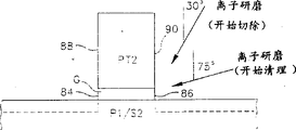
Figure 17,18 and 19 has shown and adopts two ion beams with different angles to form the sole end construction successively.Figure 17 has shown with extra thickness and has made the extreme element PT2 of portion, so that can reduce this thickness during ion beam grinds.The beginning thickness of PT2 layer can be in the magnitude of 7 μ m, and the extra thickness that wherein comprises is in the magnitude of 2 μ m.The extreme element PT2 of portion has upright side walls 88 and 90.The process that forms the extreme element PT2 of portion will be discussed in more detail below.In Figure 17, shown ion beam becomes 30 ° angular illumination with the sidewall with the extreme element PT2 of portion.Though shown ion beam only is radiated at the sidewall 90 of the extreme element PT2 of portion, owing to workpiece is rotated as described above by universal stage 130, so ion beam will be radiated on sidewall 88 and 90.Gap layer G is deposited on the P1/S2 layer, and the extreme element PT2 of portion is deposited on the gap layer G.As mentioned above, when ion beam shines straight down, quite a few material (chip) of cutting-out will be deposited on the sidewall of element of grinding again.By making ion beam become 30 °, as shown in figure 17, will have significant cutting-out, yet in downcutting operation, ion beam has also carried out chip to a certain degree and has removed with the sidewall of the extreme element PT2 of portion.30 ° of angles are best angles, yet for two angle embodiment, it can be between 20 ° and 40 °.Figure 17 has shown the beginning of excision operation, and Figure 18 has shown the end product of excision operation.In this excision operation, the extreme element PT2 of portion is used as mask when cutting out the element PT1b of the extreme portion of pedestal in secondary shielding layer S2.After 30 ° of ion beams 75 ° ion beam, as shown in figure 19, to remove the deposit again that after 30 ° of operations, still stays.75 ° of ion beams are best for removing deposit again, yet it can be in the scope that becomes 65 ° to 85 ° with the sidewall of the extreme element PT2 of portion.It should be noted, excising operating period the extra thickness (seeing Figure 17) that the thickness of the extreme element PT2 of portion has reduced to be added such as 2 μ m.Make the surprised result of people be, after this grinding, the sidewall of the extreme PT1b of portion of pedestal aligns with the sidewall of the extreme element PT2 of portion.The extreme PT1b of portion of pedestal makes by form breach 78 and 79 in secondary shielding layer S2.Gap layer G can perhaps reach its width by chemical etching by 30 ° and 75 ° of ion beams grindings before ion beam grinds.
Figure 20 and 21 has shown the embodiment that ion beam grinds, and it is similar with Figure 17,18 and 19 embodiment, and just 30 ° and 75 ° of ion beams are shone simultaneously, excise and clear operation to finish.
Figure 22 and 23 has shown the embodiment that ion beam grinds, and has wherein adopted a single ion beam to excise and remove to determine the extreme pedestal PT1b of portion.Previously described two angle ion beams are better than single ion beam.Yet, adopt single ion beam also can obtain gratifying result.For single ion beam, best angle is 55 °, yet, be that acceptable swings and encloses between 45 ° to 65 °.
Figure 24 to 28 has shown other details of the extreme portion element that is configured for Fig. 5 of the present invention and 6 embodiment.In Figure 24, adopted a photoresist figure with top magnetic pole P2 and the extreme part PT2 of portion plated film thereof.This coating operation also plated film the part beyond the figure, it is called as the P2 zone.In Figure 25, the photoresist figure is removed, and has stayed the extreme PT2 of portion, in its each side the P2 zone is arranged.In Figure 25, can see that gap layer G is deposited on the P1/S2 layer, and the extreme element PT2 of portion is deposited on the gap layer G.By this figure coating film treatment, the extreme element PT2 of portion will itself have the sidewall 88 and 90 that is vertically oriented.In Figure 26, the P2 zone has been removed and a photoresist mask has been coated over the top of utmost point spare P2, and opening or the window 140 that the extreme element PT2 of portion is exposed arranged.This photoresist window has obtained more detailed demonstration in Figure 27.As mentioned above, one or more ion beams shine by this photoresist window subsequently, as shown in figure 28, forming breach on the P1/S2 layer, thereby provide the element PT1b of the extreme portion of pedestal.
Figure 29 to 33 has shown the treatment step of the extreme portion structure of making Fig. 7 of the present invention and 8 embodiment.It is identical that these steps and Figure 24 to 28 are explained, just top magnetic pole P2 is made of two-layer, so that two extreme element PT2a of portion and PT2b to be provided, as shown in figure 30.After ion beam grinds, as shown in figure 33, formed an element PT1b of the extreme portion of pedestal and climax end construction and comprised extreme element PT2a of portion and PT2b.As mentioned above, the extreme element PT2b of portion can make with the material different with the extreme element PT2a of portion.Figure 34 has shown another embodiment, and one of them magnetosphere was set on the secondary shielding layer S2 before ion beam grinds.In the case, the sole end construction will comprise two the extreme portion of pedestal elements, i.e. PT1b and PT1c.Equally, extremely the element PT1c of portion can be made by the material different with the extreme element PT1b of portion.Extreme element PT2b of portion and PT1c can be made such as nitrided iron by height saturated material (4 π ms), and the material of extreme element PT1b of portion and PT2a can be low saturated material, such as permalloy.This height saturated material will make a large amount of magnetic flux can be by not producing saturated near the extreme portion of gap layer G.
It is apparent that now, the method of making compound MR head briefly may further comprise the steps: from ABS to and comprise the secondary shielding layer S2 of post gap deposit read head, thereby make the S2 layer have extreme portion part and the rear portion (seeing Fig. 5 and 6) between zero larynx height and post gap between ABS and zero larynx height; From ABS to zero larynx height, deposit gap layer G on secondary shielding layer S2 (seeing Fig. 5 and 6); Deposit magnetosphere on gap layer G and secondary shielding layer S2, thus on gap layer G, form have the extreme element PT2 of portion top magnetic pole P2 (seeing Figure 24 and 25); And, utilize the extreme element PT2 of portion as mask, along with the parallel substantially direction of ABS and with first and second sidewalls 88 and 90 of the extreme element PT2 of portion at an angle, with at least one ion beam irradiation on the extreme portion part of secondary shielding layer S2, on the S2 layer, form breach so that be offset each side 78 and 79 in extreme portion element PT2 road, these breach form a pedestal on secondary shielding layer S2, this pedestal is utmost point end layers PT1b, and remove the element PT1b's of the extreme portion of pedestal, secondary shielding layer S2 between ABS and zero larynx height is the extreme element PT1a of portion (seeing Figure 17 to 19), the first side wall 80 and 88 of extreme PT1b of portion and PT2 aligns in first perpendicular 100, and second sidewall 82 and 90 of extreme PT1b of portion and PT2 aligns in second perpendicular 102, first and second upright side walls 100 and 102 apart with the wide w (see figure 6) in the road that determines compound MR head at ABS.The step of shining with at least one ion beam can comprise first and second ion beams, and first ion beam is in the angle θ in the scope of 0 °<θ<60 °, and second ion beam is in the angle θ in the scope of 60 °≤θ≤85 °.The step of deposit gap layer G can comprise clearance layer is set, and this clearance layer has suitable thickness, and this thickness defines the length g in 0.1 μ m to 0.7 mu m range, and the extreme element PT1b of portion is in the scope of length at 0.5g to 3.0g at ABS place.The step of shining with at least one ion beam can be included in secondary shielding layer S2 and go up 78 and 79 and form breach, so that each breach is approximately 0.7 μ m is dark, thereby the length of about 0.7 μ m is provided for the extreme element PT1b of portion; And make the bed thickness of the extreme element PT2 of portion reduce about 2 μ m with the step that at least one ion beam shines.
Be apparent that now above-mentioned discovery makes compound MR head can have vertical aligning, adjacent with clearance layer extreme portion, and the sole end member is a pedestal with respect to the secondary shielding layer S2 of compound MR read head.The vertical aligning of sidewall makes that the side direction between the extreme portion writes reduces to have reached the best.
Obviously, other embodiment of the present invention and correction are conspicuous for those of skill in the art.Therefore, the present invention only is limited by the accompanying claims, and when seeing in conjunction with above instructions and accompanying drawing, these claims have comprised all this embodiment and corrections.

Claims (28)

1. make the method that compound magnetoelectric hinders head for one kind, this compound magnetoelectric resistance head comprises that a magneto-resistor reads head and a write head, this magneto-resistor reads head and comprises first and second screen layer S1 and the S2, be clipped in first and second gap layer G 1 and the G2 between the first and second screen layer S1 and the S2, and be clipped in a magnetoresistive element between first and second gap layer G 1 and the G2, and this write head comprises the end and climax spare P1 and the P2 that extends to and comprise a post gap from an air bearing surface (ABS), bottom pole piece P1 comprises secondary shielding layer S2, bottom pole piece P1 has extreme element PT1a of portion and the PT1b that extends between ABS and one zero larynx height, the extreme element PT1b of portion is with respect to secondary shielding layer S2, sole P1 and the extreme element PT1a of portion are pedestals, secondary shielding layer S2 comprises PT1a and PT1b, be clipped in the gap layer G between extreme element PT1b of portion and the PT2, with each extreme element PT2 of portion, gap layer G and the extreme element PT1b of portion have first and second upright side walls, the extreme element PT2 of portion, first upright side walls of gap layer G and the extreme element PT1b of portion is arranged in one first perpendicular in abutting connection with ground, and the extreme element PT2 of portion, second upright side walls of gap layer G and the extreme element PT1b of portion is arranged in one second perpendicular in abutting connection with ground, this first and second upright side walls and ABS is perpendicular and at the ABS place each other at a distance of one wide apart from w with the road of determining compound magnetoelectric resistance head, this manufacture method is characterised in that and comprises:
At least one magnetosphere of deposit is to form secondary shielding layer S2 and bottom pole piece P1 that a magneto-resistor reads head, this bottom pole piece P1 extends to and comprises that a post gap, this bottom pole piece P1 have the extreme portion of the not qualification part of extending between ABS and one zero larynx height from an air bearing surface (ABS);
On a described magnetosphere from ABS to zero larynx height deposit gap layer G;
Another magnetosphere of deposit with on bottom pole piece P1, form from ABS to and comprise the climax spare P2 of post gap, this climax spare P2 has the extreme element PT2 of portion of a qualification, and this extreme element PT2 of portion extends between ABS and zero larynx height and has first and second upright side walls; And
Become the extreme portion of the not qualification part of the angular illumination bottom pole piece P1 of θ with sidewall with the extreme element PT2 of portion that limits with at least one ion beam, utilize the extreme element PT2 of portion that limits as mask, each side at the extreme element PT2 of portion forms vertical breach so that bottom pole piece P1 forms extreme element PT1a of portion and PT1b on bottom pole piece P1, extremely the element PT1b of portion is with respect to the pedestal of bottom pole piece P1 and has respectively first and second upright side walls that first and second upright side walls with the extreme element PT2 of portion align.
2. according to the method for claim 1, it is characterized in that comprising:
Before the extreme portion part that does not limit with at least one ion beam irradiation bottom pole piece P1, photoresist mask of deposit on climax spare P2;
An opening is provided on this photoresist mask, this opening exposes and limits the extreme element PT2 of portion and in a zone of its each side, so that the extreme element PT2 of portion that limits can be as with the extreme portion of not limiting of at least one ion beam irradiation bottom pole piece P1 mask partly.
3. according to the method for claim 1, it is characterized in that comprising:
Step with at least one ion beam irradiation is included in the extreme portion of the not qualification of this ion beam irradiation bottom pole piece P1 part before with this ion beam irradiation gap layer G; And
Step with at least one ion beam shines provides first and second upright side walls to gap layer G, and this first and second upright side walls aligns with first and second upright side walls of extreme element PT1b of portion and PT2 respectively.
4. according to the method for claim 4, it is characterized in that comprising:
The step of deposit gap layer G provides the thickness in 0.1 μ m to 0.7 mu m range to clearance layer at the ABS place; And
The length of the element PT1b of the extreme portion in ABS place is 2.0g.
5. according to the method for claim 1, it is characterized in that comprising:
The step of shining with at least one ion beam comprises with a single ion beam shines with a single angle θ.
6. according to the method for claim 1, it is characterized in that comprising:
The step of shining with at least one ion beam comprises with first and second ion beams shines;
First ion beam is in the angle θ in ° scope of 0 °<θ<60; And
Second ion beam is in the angle θ in ° scope of 60 °<θ<85.
7. according to the method for claim 6, it is characterized in that comprising:
First ion beam is in the angle θ in ° scope of 20 °<θ<40.
8. according to the method for claim 7, it is characterized in that comprising:
It is 30 ° angle θ that first ion beam is in; And
It is 75 ° angle θ that second ion beam is in.
9. according to the method for claim 1, it is characterized in that comprising:
Reduced the thickness of utmost point end layers PT2 with the step of at least one ion beam irradiation; And
The step of the element PT2 of the extreme portion of deposit comprises the step with an additional thickness deposit utmost point end layers PT2, and this additional thickness equals the decrease of the extreme element PT2 of the portion thickness that step caused that shines with at least one ion beam.
10. according to the method for claim 9, it is characterized in that comprising:
Before the step of shining with at least one ion beam, at mask of deposit on the utmost point spare P2 layer between zero larynx height and the post gap, and on the mask between ABS and the zero larynx height, reserving a window, with the extreme element PT2 of portion of exposure qualification and a zone of each side thereof.
11., it is characterized in that comprising according to the method for claim 10:
The step of shining with at least one ion beam comprises with a single ion beam shines with a single angle θ; And
Angle θ is in the scope of 0 °<θ<60 °.
12., it is characterized in that comprising according to the method for claim 10:
The step of shining with at least one ion beam comprises with first and second ion beams shines;
First ion beam is in the angle θ in ° scope of 20 °<θ<40; And
Second ion beam is in the angle θ in ° scope of 65 °<θ<85.
13., it is characterized in that comprising according to the method for claim 12:
It is 30 ° angle θ that first ion beam is in; And
It is 75 ° angle θ that second ion beam is in.
14., it is characterized in that comprising according to the method for claim 13:
The step of deposit gap layer G provides a layer thickness, and this thickness provides a length g at the ABS place to clearance G; And
The length of the element PT1b of the extreme portion in ABS place is 2.0g.
15., it is characterized in that comprising according to the method for claim 14:
Shine in the time of first and second ion beams.
16., it is characterized in that comprising according to the method for claim 14:
First and second ion beams shine successively.
17., it is characterized in that comprising according to the method for claim 16:
The step of shining with at least one ion beam comprises that the bottom pole piece P1 that will have deposit layer thereon is placed in the ion beam grinding chamber, and, use ion beam irradiation bottom pole piece P1 and deposit layer thereon simultaneously with constant rotational speed bottom pole piece P1 and deposit layer thereon.
18., it is characterized in that comprising according to the method for claim 17:
The step of deposit gap layer G comprises to gap layer G provides a length g in 0.1 μ m to 0.7 mu m range;
The step of described another magnetosphere of deposit comprises that deposit has the extreme element PT2 of portion of the layer thickness that is 7 μ m;
The step of shining with at least one ion beam is included in bottom pole piece P1 and goes up and form breach so that each breach to be 0.7 μ m dark and pedestal to have be 0.7 μ m, highly; And
The step of shining with at least one ion beam can make the thickness of the extreme element PT2 of portion reduce 2 μ m.
19. method of making compound magnetoelectric resistance head, this compound magnetoelectric resistance head comprises that a magneto-resistor reads head and a write head, this magneto-resistor reads head and comprises first and second screen layer S1 and the S2, be clipped in first and second gap layer G 1 and the G2 between the first and second screen layer S1 and the S2, and be clipped in a magnetoresistive element between first and second gap layer G 1 and the G2, and this write head comprises the end and climax spare P1 and the P2 that extends to and comprise a post gap from an air bearing surface (ABS), bottom pole piece P1 comprises secondary shielding layer S2, bottom pole piece P1 has extreme element PT1a of portion and the PT1b that extends between ABS and one zero larynx height, the extreme element PT1b of portion is with respect to secondary shielding layer S2, sole P1 and the extreme element PT1a of portion are pedestals, secondary shielding layer S2 comprises PT1a and PT1b, be clipped in the gap layer G between extreme element PT1b of portion and the PT2, with each extreme element PT2 of portion, gap layer G and the extreme element PT1b of portion have first and second upright side walls, the extreme element PT2 of portion, first upright side walls of gap layer G and the extreme element PT1b of portion is arranged in one first perpendicular in abutting connection with ground, and the extreme element PT2 of portion, second upright side walls of gap layer G and the extreme element PT1b of portion is arranged in one second perpendicular in abutting connection with ground, this first and second upright side walls and ABS is perpendicular and at the ABS place each other at a distance of one wide apart from w with the road of determining compound magnetoelectric resistance head, this manufacture method is characterised in that and comprises:
One of deposit from ABS to and comprise first magnetosphere of post gap, to form:
(1) magneto-resistor read the head secondary shielding layer S2 and
(2) sole P1, it has at one between ABS and the zero larynx height and does not limit an extreme portion part and a rear portion between zero larynx height and post gap;
The gap layer G of deposit on first magnetosphere from ABS to zero larynx height;
At one second magnetosphere of deposit on the gap layer G and above first magnetosphere, to form climax spare P2, this climax spare P2 has the extreme element PT2 of portion that has first and second upright side walls; And
Use at least one ion beam, along substantially parallel with ABS and with first and second upright side walls of the extreme element PT2 of the portion direction of θ at an angle, and utilize the extreme element PT2 of portion as mask, shine the zone that does not limit extreme portion part of sole P1 on first magnetosphere, on each side of the extreme element PT2 of portion, to form breach on first magnetosphere, these breach make first magnetosphere have a vertical pedestal, this vertical pedestal is the extreme element PT1b of portion, this extreme element PT1b of portion has first and second upright side walls, and between ABS and zero larynx height, magnetosphere except pedestal comprises the extreme element PT1a of portion, first upright side walls of extreme element PT1b of portion and PT2 is aligned with each other in one first perpendicular, and second sidewall of extreme PT1b of portion and PT2 is aligned with each other in one second perpendicular, this first and second upright side walls vertical with ABS and at ABS place each other at a distance of the wide w in road that hinders with the qualification compound magnetoelectric.
20., it is characterized in that comprising according to the method for claim 19:
The step of shining with at least one ion beam is included in using the ion beam irradiation gap layer G before the extreme portion of the ion beam irradiation end qualification part; And
The step of shining with at least one ion beam provides first and second upright side walls to gap layer G, and this first and second upright side walls aligns with first and second upright side walls of extreme element PT1b of portion and PT2 respectively.
21., it is characterized in that comprising according to the method for claim 19:
The step of shining with an ion beam comprises uses first and second ion beam irradiations;
First ion beam is in the angle θ in the scope of 20 °<θ<40 °; And
Second ion beam is in the angle θ in the scope of 65 °<θ<85 °.
22., it is characterized in that comprising according to the method for claim 21:
The step of shining with first and second ion beams reduces the thickness of the extreme element PT2 of portion; And
The deposit magnetosphere comprises that with the step that forms the extreme element PT2 of portion deposit has the extreme element PT2 of portion of additional thickness, and this additional thickness equals the decrease of the extreme element PT2 of the portion thickness that step caused that shines with at least one ion beam; And
Before shining with first and second ion beams, at mask of deposit between zero larynx height and post gap substantially on the magnetic pole P2 of top, and reserving a window between ABS and the zero larynx height with the extreme element PT2 of portion that exposes qualification and a zone of each side thereof on this mask.
23., it is characterized in that comprising according to the method for claim 22:
The step of deposit gap layer G provides a layer thickness, and this layer thickness provides a length g at the ABS place for clearance G; And
The length of the element PT1b of the extreme portion in ABS place is in the scope of 0.5g to 3.0g.
24., it is characterized in that comprising according to the method for claim 23:
It is 30 ° angle θ that first ion beam is in; And
It is 75 ° angle θ that second ion beam is in.
25., it is characterized in that comprising according to the method for claim 24:
The step of deposit gap layer G comprises that deposit has the gap layer G of the thickness g in 0.1 μ m to 0.7 mu m range;
The step of the element PT2 of the extreme portion of deposit comprises that deposit has the extreme element PT2 of portion of the layer thickness that is 7 μ m;
The step of shining with first and second ion beams is included in and forms the degree of depth on first magnetosphere is the breach of 0.7 μ m, thereby the pedestal with the height that is 0.7 μ m is provided; And
The step of shining with first and second ion beams makes the layer thickness of the extreme element PT2 of portion reduce 2 μ m.
26., it is characterized in that comprising according to the method for claim 25:
The step of shining with first and second ion beams comprises first magnetosphere and deposit layer thereon is placed in the ion beam grinding chamber, and with this first magnetosphere of constant rotational speed and deposit layer thereon, and simultaneously with this first magnetosphere of ion beam irradiation and deposit layer thereon.
27., it is characterized in that comprising according to the method for claim 26:
First and second ion beams shine simultaneously.
28., it is characterized in that comprising according to the method for claim 26
First and second ion beams shine successively.
CN94112929A 1994-03-09 1994-12-09 Thin film merged MR head with aligned pole tips Expired - Fee Related CN1058800C (en)

Applications Claiming Priority (2)

Application Number Priority Date Filing Date Title
US08/208,398 US5438747A (en) 1994-03-09 1994-03-09 Method of making a thin film merged MR head with aligned pole tips
US208,398 1994-03-09

Publications (2)

Publication Number Publication Date
CN1122496A CN1122496A (en) 1996-05-15
CN1058800C true CN1058800C (en) 2000-11-22

Family

ID=22774467

Family Applications (1)

Application Number Title Priority Date Filing Date
CN94112929A Expired - Fee Related CN1058800C (en) 1994-03-09 1994-12-09 Thin film merged MR head with aligned pole tips

Country Status (8)

Country Link
US (1) US5438747A (en)
EP (1) EP0671725A2 (en)
JP (1) JP3045941B2 (en)
KR (1) KR0150385B1 (en)
CN (1) CN1058800C (en)
MY (1) MY111561A (en)
SG (1) SG28470A1 (en)
TW (1) TW247363B (en)

Cited By (1)

* Cited by examiner, † Cited by third party
Publication number Priority date Publication date Assignee Title
CN1326116C (en) * 2004-04-02 2007-07-11 Tdk株式会社 Composite type thin-film magnetic head

Families Citing this family (156)

* Cited by examiner, † Cited by third party
Publication number Priority date Publication date Assignee Title
EP0640955B1 (en) * 1993-08-27 1999-05-19 Read-Rite Corporation Magnetic head assembly with write pole/shield structure
US5633771A (en) * 1993-09-29 1997-05-27 Kabushiki Kaisha Toshiba Magnetoresistance effect type head and separate recording-reproducing type magnetic head
JP2854513B2 (en) * 1993-10-21 1999-02-03 アルプス電気株式会社 Composite thin-film magnetic head and method of manufacturing the same
US5739991A (en) * 1994-02-01 1998-04-14 Sanyo Electric Co., Ltd. Composite thin film head having magnetoresistive and inductive head portions with nonmagnetic thin film interposed between core and shield portions of core layer
US5452164A (en) * 1994-02-08 1995-09-19 International Business Machines Corporation Thin film magnetic write head
US5557491A (en) * 1994-08-18 1996-09-17 International Business Machines Corporation Two terminal single stripe orthogonal MR head having biasing conductor integral with the lead layers
US5606478A (en) * 1994-12-08 1997-02-25 International Business Machines Corporation Ni45 Fe55 metal-in-gap thin film magnetic head
EP0835507A4 (en) * 1995-06-05 1998-09-09 Quantum Peripherals Colorado Flux enhanced write transducer and process for producing the same in conjunction with shared shields on magnetoresistive read heads
US5578342A (en) * 1995-07-05 1996-11-26 Read-Rite Corporation Alignment of magnetic poles of thin film transducer
WO1997008687A1 (en) * 1995-08-23 1997-03-06 Hitachi, Ltd. Magnetic head and magnetic memory apparatus using the head
US5734531A (en) * 1995-10-31 1998-03-31 Quantum Peripherals Colorado, Inc. Magneto-resistive read/write head having a combination pole/shield
US5784772A (en) * 1995-12-21 1998-07-28 Storage Technology Corporation Method of simultaneously forming MR sensors in a dual element MR head
US6545847B2 (en) * 1996-02-14 2003-04-08 Hitachi, Ltd. Magnetoresistive effect head
JPH09293209A (en) * 1996-04-26 1997-11-11 Fujitsu Ltd Thin film magnetic head and magnetic recorder and production of thin film magnetic head
JP3349925B2 (en) * 1996-09-10 2002-11-25 アルプス電気株式会社 Method for manufacturing thin film magnetic head
JP2953401B2 (en) * 1996-10-04 1999-09-27 日本電気株式会社 Manufacturing method of magnetoresistive composite head
US5864450A (en) * 1996-10-09 1999-01-26 International Business Machines Corporation NI45FE55 metal-in-gap thin film magnetic head
JP2980041B2 (en) * 1996-11-26 1999-11-22 日本電気株式会社 Method of manufacturing composite head
US6034847A (en) * 1996-12-25 2000-03-07 Hitachi, Ltd. Apparatus and thin film magnetic head with magnetic membrane layers of different resistivity
US5804085A (en) * 1997-01-30 1998-09-08 Quantum Corporation Process for producing a pole-trimmed writer in a magnetoresistive read/write head and a data transducer made thereby
JPH10247305A (en) * 1997-03-03 1998-09-14 Sanyo Electric Co Ltd Production of composite type thin-film magnetic head
JP2914343B2 (en) * 1997-04-07 1999-06-28 日本電気株式会社 Magnetoresistive head, method of manufacturing the same, and magnetic storage
US5875542A (en) * 1997-04-18 1999-03-02 Read-Rite Corporation Method of making thin film merged magnetoresistive heads
JPH117608A (en) * 1997-04-25 1999-01-12 Fujitsu Ltd Magnetic head and its manufacture
US5878481A (en) * 1997-04-28 1999-03-09 Headway Technologies, Inc. Pole trimming method for fabricating a magnetic transducer structure
US5916423A (en) * 1997-05-06 1999-06-29 International Business Machines Corporation P1 notched write head with minimum overmilled p1 and p2
US5768070A (en) 1997-05-14 1998-06-16 International Business Machines Corporation Horizontal thin film write, MR read head
JPH10334409A (en) * 1997-05-27 1998-12-18 Tdk Corp Thin film magnetic head
US6178065B1 (en) 1997-05-29 2001-01-23 Tdk Corporation Thin film magnetic head and manufacturing method of the head
JPH10334410A (en) 1997-05-29 1998-12-18 Tdk Corp Thin film magnetic head and its manufacture
US6201670B1 (en) 1997-06-16 2001-03-13 International Business Machines Corporation Merged magnetic head that includes a write head with single-sided notched first pole piece
US6119331A (en) * 1997-07-08 2000-09-19 International Business Machines Corporation Notching the first pole piece of a write head with a notching layer in a combined magnetic head
JPH1131308A (en) * 1997-07-08 1999-02-02 Nec Ibaraki Ltd Mr composite head and its manufacture
US6031695A (en) 1997-09-05 2000-02-29 International Business Machines Corporation Combined read head and write head with non-magnetic electrically conductive layer on upper pole tip thereof
JPH1186238A (en) * 1997-09-10 1999-03-30 Fujitsu Ltd Magnetic head
JP3369444B2 (en) * 1997-09-12 2003-01-20 ティーディーケイ株式会社 Thin film magnetic head
US5905608A (en) * 1997-09-19 1999-05-18 International Business Machines Corporation Dynamically tuned outer arms for improved rotary actuator performance
JP3795236B2 (en) 1997-10-01 2006-07-12 Tdk株式会社 Thin film magnetic head
US6018862A (en) * 1997-10-07 2000-02-01 Seagate Technology, Inc. Thin-film magnetic recording head using a plated metal gap layer
US20040168302A1 (en) * 1997-10-15 2004-09-02 Tdk Corporation Method for manufacturing thin-film magnetic head
US5940250A (en) * 1997-10-21 1999-08-17 Maxtor Corporation Disk drive head having a read wide/write narrow architecture
JP3484332B2 (en) 1997-11-11 2004-01-06 Tdk株式会社 Method for manufacturing thin-film magnetic head
JP3790347B2 (en) 1997-11-26 2006-06-28 Tdk株式会社 Manufacturing method of thin film magnetic head
US6105238A (en) * 1997-12-04 2000-08-22 Matsushita-Kotobukie Electronics Industries, Ltd. Method and structure for defining track width on a recording head
US6024886A (en) * 1997-12-05 2000-02-15 Headway Technologies, Inc. Planarizing method for fabricating an inductive magnetic write head for high density magnetic recording
JPH11232610A (en) 1997-12-12 1999-08-27 Tdk Corp Thin-film magnetic head
US5867890A (en) * 1997-12-17 1999-02-09 International Business Machines Corporation Method for making a thin film merged magnetoresistive read/inductive write head having a pedestal pole tip
US6069775A (en) * 1997-12-22 2000-05-30 International Business Machines Corporation Inverted merged MR head with precise track width
US5901432A (en) * 1997-12-24 1999-05-11 International Business Machines Corporation Method for making a thin film inductive write head having a pedestal pole tip and an electroplated gap
JPH11203627A (en) * 1998-01-12 1999-07-30 Tdk Corp Thin film magnetic head
US5996213A (en) * 1998-01-30 1999-12-07 Read-Rite Corporation Thin film MR head and method of making wherein pole trim takes place at the wafer level
JP3782228B2 (en) * 1998-02-27 2006-06-07 Tdk株式会社 Composite thin film magnetic head and method for manufacturing the same
US6024884A (en) * 1998-03-12 2000-02-15 Storage Technology Corporation Method for creating microstructures
JPH11288503A (en) 1998-04-02 1999-10-19 Tdk Corp Thin-film magnetic head and its production
US6158107A (en) * 1998-04-02 2000-12-12 International Business Machines Corporation Inverted merged MR head with plated notched first pole tip and self-aligned second pole tip
US6172848B1 (en) 1998-04-10 2001-01-09 International Business Machines Corporation Write head with self aligned pedestal shaped pole tips that are separated by a zero throat height defining layer
US6317289B1 (en) 1998-04-17 2001-11-13 Tdk Corporation Combination-type thin film magnetic head with improved writing properties
US6034848A (en) 1998-04-22 2000-03-07 International Business Machines Corporation Low profile multi-layer coil merged thin film magnetic head
US6055138A (en) * 1998-05-06 2000-04-25 Read-Rite Corporation Thin film pedestal pole tips write head having narrower lower pedestal pole tip
JPH11328647A (en) * 1998-05-12 1999-11-30 Hitachi Ltd Magnetic recording medium and manufacture of magnetic recording medium
JPH11339223A (en) 1998-05-26 1999-12-10 Tdk Corp Etchig method of magnetic layer, formation of magnetic pole for thin-film magnetic head and manufacture of thin-film magnetic head
JPH11353616A (en) 1998-06-11 1999-12-24 Tdk Corp Thin-film magnetic head and its production
US6510024B2 (en) 1998-06-30 2003-01-21 Fujitsu Limited Magnetic head and method of manufacturing the same
JP3755560B2 (en) 1998-06-30 2006-03-15 富士通株式会社 Magnetic head and manufacturing method thereof
JP3428905B2 (en) 1998-06-30 2003-07-22 ティーディーケイ株式会社 Metal film forming method and pole forming method for thin film magnetic head
JP2000020916A (en) 1998-07-01 2000-01-21 Hitachi Ltd Induction type thin-film magnetic head
JP2000105907A (en) 1998-07-30 2000-04-11 Tdk Corp Thin film magnetic head and manufacture thereof
JP3469473B2 (en) 1998-08-26 2003-11-25 Tdk株式会社 Thin film magnetic head and method of manufacturing the same
US6317288B1 (en) 1998-08-28 2001-11-13 Tdk Corporation Thin-film magnetic head and method of manufacturing same
JP3306011B2 (en) 1998-09-22 2002-07-24 日本電気株式会社 Magnetoresistive composite head and method of manufacturing the same
JP3503874B2 (en) 1998-09-29 2004-03-08 Tdk株式会社 Method for manufacturing thin-film magnetic head
JP2000113412A (en) 1998-10-07 2000-04-21 Tdk Corp Thin film magnetic head and manufacture thereof
JP3180906B2 (en) * 1998-11-12 2001-07-03 日本電気株式会社 Manufacturing method of magnetoresistive composite head
JP2000149219A (en) * 1998-11-12 2000-05-30 Tdk Corp Thin film magnetic head and its manufacture
JP3523092B2 (en) 1998-11-18 2004-04-26 Tdk株式会社 Thin film magnetic head and method of manufacturing the same
JP3781399B2 (en) 1998-12-08 2006-05-31 Tdk株式会社 Thin film magnetic head and manufacturing method thereof
US6176005B1 (en) * 1998-12-15 2001-01-23 International Business Machines Corporation Method of making read head with improved lead layers
US6765756B1 (en) 1999-03-12 2004-07-20 Western Digital (Fremont), Inc. Ultra-short yoke and ultra-low stack height writer and method of fabrication
US6464891B1 (en) 1999-03-17 2002-10-15 Veeco Instruments, Inc. Method for repetitive ion beam processing with a carbon containing ion beam
JP3373167B2 (en) 1999-03-24 2003-02-04 ティーディーケイ株式会社 Method for manufacturing thin-film magnetic head
JP3530064B2 (en) 1999-03-29 2004-05-24 Tdk株式会社 Thin-film magnetic head, method of manufacturing the same, material for thin-film magnetic head, and method of manufacturing the same
US6238582B1 (en) * 1999-03-30 2001-05-29 Veeco Instruments, Inc. Reactive ion beam etching method and a thin film head fabricated using the method
JP3856587B2 (en) 1999-04-06 2006-12-13 Tdk株式会社 Thin film magnetic head and manufacturing method thereof
US6282056B1 (en) 1999-04-08 2001-08-28 Read-Rite Corporation Tapered stitch pole writer for high density magnetic recording
US6657816B1 (en) * 1999-04-09 2003-12-02 Ronald A. Barr Thin film inductive read/write head with a sloped pole
JP3856591B2 (en) 1999-04-28 2006-12-13 Tdk株式会社 Thin film magnetic head and manufacturing method thereof
US6224719B1 (en) * 1999-05-13 2001-05-01 International Business Machines Corporation Sputtering method of manufacturing Fe-Ai-N-O laminated films using N2O as the reactive gas
JP3421635B2 (en) 1999-06-04 2003-06-30 ティーディーケイ株式会社 Thin film magnetic head and method of manufacturing the same
US6342990B1 (en) 1999-06-14 2002-01-29 Tdk Corporation Method for forming magnetic pole layer of thin film magnetic head, thin film magnetic head and method for manufacturing the same
JP3522593B2 (en) 1999-06-15 2004-04-26 Tdk株式会社 Thin film magnetic head and method of manufacturing the same
JP3527138B2 (en) * 1999-06-17 2004-05-17 Tdk株式会社 Thin-film magnetic head and method of manufacturing the same, thin-film coil element and method of manufacturing the same
JP3526787B2 (en) 1999-06-25 2004-05-17 Tdk株式会社 Thin film magnetic head and method of manufacturing the same
JP3859398B2 (en) 1999-07-08 2006-12-20 Tdk株式会社 Thin film magnetic head and manufacturing method thereof
US7012784B2 (en) * 1999-07-08 2006-03-14 Tdk Corporation Thin-film magnetic head and method of manufacturing same
JP3373176B2 (en) * 1999-07-09 2003-02-04 ティーディーケイ株式会社 Method of manufacturing thin-film magnetic head and thin-film magnetic head
JP3490643B2 (en) 1999-07-14 2004-01-26 Tdk株式会社 Method for manufacturing thin-film magnetic head
JP3522595B2 (en) 1999-07-14 2004-04-26 Tdk株式会社 Thin film magnetic head and method of manufacturing the same
JP2001034911A (en) 1999-07-16 2001-02-09 Tdk Corp Thin film magnetic head and fabrication method thereof
JP2001043510A (en) * 1999-07-30 2001-02-16 Fujitsu Ltd Magnetic head and manufacture of the same
JP3473684B2 (en) 1999-11-08 2003-12-08 日本電気株式会社 Magnetic head, method of manufacturing the same, and magnetic recording / reproducing apparatus using the same
JP2001067617A (en) 1999-08-24 2001-03-16 Tdk Corp Thin film magnetic head and its manufacture
US6317290B1 (en) 1999-08-31 2001-11-13 Read-Rite Corporation Advance pole trim writer with moment P1 and low apex angle
US6452742B1 (en) 1999-09-02 2002-09-17 Read-Rite Corporation Thin film write having reduced resistance conductor coil partially recessed within middle coat insulation
JP3530084B2 (en) 1999-09-07 2004-05-24 Tdk株式会社 Thin film magnetic head and method of manufacturing the same
JP2001084514A (en) 1999-09-16 2001-03-30 Tdk Corp Thin film magnetic head and manufacture thereof
US6791794B2 (en) 2000-09-28 2004-09-14 Nec Corporation Magnetic head having an antistripping layer for preventing a magnetic layer from stripping
US6243939B1 (en) 1999-10-04 2001-06-12 Headway Technologies, Inc. High ion beam etch selectivity for partial pole trim application
JP3492953B2 (en) * 1999-10-05 2004-02-03 Tdk株式会社 Method for manufacturing thin-film magnetic head
JP2001110008A (en) 1999-10-06 2001-04-20 Nec Corp Magnetic head and its production, and magnetic recording and reproducing device
JP3869595B2 (en) * 1999-11-12 2007-01-17 Tdk株式会社 Thin film magnetic head and manufacturing method thereof
US6460243B1 (en) * 1999-11-22 2002-10-08 International Business Machines Corporation Method of making low stress and low resistance rhodium (RH) leads
JP3440224B2 (en) 1999-11-29 2003-08-25 Tdk株式会社 Thin film magnetic head and method of manufacturing the same
US7002776B2 (en) 1999-12-06 2006-02-21 Tdk Corporation Thin film magnetic head and method of manufacturing same
JP2001167406A (en) 1999-12-07 2001-06-22 Tdk Corp Thin-film magnetic head method for manufacturing the same
JP2001167408A (en) 1999-12-09 2001-06-22 Tdk Corp Thin-film magnetic head and method for manufacturing the same
JP3440225B2 (en) 1999-12-09 2003-08-25 Tdk株式会社 Frame plating method and method of forming magnetic pole of thin film magnetic head
US6594112B1 (en) * 2000-01-05 2003-07-15 Seagate Technology Llc Magnetic recording head with a precision throatheight-defining structure
JP2001195706A (en) 2000-01-05 2001-07-19 Nec Corp Recording head, method for manufacturing recording head and composite head as well as magnetic recording and reproducing device
JP3565492B2 (en) 2000-02-17 2004-09-15 Tdk株式会社 Thin-film magnetic head, magnetic head device, and magnetic disk device
US6687096B2 (en) 2000-06-21 2004-02-03 Tdk Corporation Thin-film magnetic head and method of manufacturing same
JP2002015405A (en) * 2000-06-28 2002-01-18 Tdk Corp Thin film magnetic head and method of manufacture
JP2002015404A (en) 2000-06-29 2002-01-18 Tdk Corp Thin film magnetic head and method of manufacture
US6539610B1 (en) 2000-07-14 2003-04-01 International Business Machines Corporation Method for manufacturing a magnetic write head
JP2002063703A (en) 2000-08-18 2002-02-28 Tdk Corp Method for forming thin film pattern, and method for forming magnetic pole of thin film magnetic head
JP3617953B2 (en) 2000-09-18 2005-02-09 Tdk株式会社 Manufacturing method of thin film magnetic head
JP2002170208A (en) * 2000-11-22 2002-06-14 Shinka Jitsugyo Kk Thin-film magnetic head and its manufacturing method
JP3593312B2 (en) 2000-12-26 2004-11-24 アルプス電気株式会社 Perpendicular magnetic recording head and method of manufacturing the same
US6765757B2 (en) * 2001-01-15 2004-07-20 Alps Electric Co., Ltd. Soft magnetic film having high saturation magnetic flux density, thin-film magnetic head using the same, and manufacturing method of the same
JP4176322B2 (en) * 2001-03-26 2008-11-05 Tdk株式会社 Thin film forming method and thin film magnetic head manufacturing method
US6654203B2 (en) 2001-04-25 2003-11-25 Tdk Corporation Thin-film magnetic head and method of manufacturing same, head gimbal assembly and hard disk drive
US6678117B2 (en) 2001-06-18 2004-01-13 Hitachi Global Storage Technologies Netherlands B.V. Magnetic transducer with bilayer pole piece structure with improved milling endpoint detection
US6656371B2 (en) * 2001-09-27 2003-12-02 Micron Technology, Inc. Methods of forming magnetoresisitive devices
US6656372B2 (en) * 2001-10-04 2003-12-02 Micron Technology, Inc. Methods of making magnetoresistive memory devices
US6947255B2 (en) * 2002-03-22 2005-09-20 International Business Machines Corporation Magnetic head having a notched pole piece structure and method of making the same
JP2004127404A (en) * 2002-10-01 2004-04-22 Tdk Corp Thin film magnetic head, magnetic head device, and magnetic recording and reproducing device
JP3865308B2 (en) * 2002-10-02 2007-01-10 Tdk株式会社 Thin film magnetic head, magnetic head device, and magnetic recording / reproducing device
US6887355B2 (en) * 2002-10-31 2005-05-03 Headway Technologies, Inc. Self-aligned pole trim process
US20050034298A1 (en) * 2003-08-15 2005-02-17 Hitachi Global Storage Technologies Disk drive yield optimization by capacity
US7133255B2 (en) * 2003-08-27 2006-11-07 Hitachi Global Storage Technologies Netherlands, B.V. Magnetic head having magnetic pole with lengthened neck pole tip and coplanar yoke, and method of fabrication thereof
US7086139B2 (en) * 2004-04-30 2006-08-08 Hitachi Global Storage Technologies Netherlands B.V. Methods of making magnetic write heads using electron beam lithography
US7480983B2 (en) * 2004-05-28 2009-01-27 Hitachi Global Storage Technologies Netherlands B.V. Method for making magnetic write head
US8815060B2 (en) * 2004-08-30 2014-08-26 HGST Netherlands B.V. Method for minimizing magnetically dead interfacial layer during COC process
US7363698B2 (en) * 2004-09-30 2008-04-29 Hitachi Gobal Storage Technologies Inc. Process for creating a write head by forming a bump after the top pole is formed
JP2007184022A (en) 2006-01-04 2007-07-19 Alps Electric Co Ltd Manufacturing method of main magnetic pole of perpendicular magnetic recording head
US7969684B2 (en) * 2006-03-28 2011-06-28 Hitachi Global Storage Technologies Netherlands B.V. Write head design and method for reducing adjacent track interference at very narrow track widths
US7536774B2 (en) * 2006-04-07 2009-05-26 Hitachi Global Storage Technologies B.V. Method and apparatus for integrating a stair notch and a gap bump at a pole tip in a write head
US7768741B2 (en) * 2006-05-22 2010-08-03 Hitachi Global Storage Technologies Netherlands B.V. Magnetic write head design for reducing wide area track erasure
US7716813B2 (en) * 2006-12-05 2010-05-18 Hitachi Global Storage Technologies Netherlands B.V. Method for fabricating magnetic write pole for a magnetic head using an E-beam resist mask
US8361284B2 (en) * 2007-05-03 2013-01-29 Hgst, Netherlands B.V. Reducing the height of a defect associated with an air bearing surface
US20090273859A1 (en) * 2008-05-02 2009-11-05 Flint Eric W Forming a pole tip topography
US8080167B2 (en) 2009-02-20 2011-12-20 Tdk Corporation Shaping method of thin film and manufacturing method of perpendicular recording magnetic head using the same
US8790524B1 (en) 2010-09-13 2014-07-29 Western Digital (Fremont), Llc Method and system for providing a magnetic recording transducer using a line hard mask and a wet-etchable mask
CA2791249C (en) 2011-11-10 2014-02-25 Semiconductor Insights Inc. Method and system for ion beam delayering of a sample and control thereof
US8607438B1 (en) 2011-12-01 2013-12-17 Western Digital (Fremont), Llc Method for fabricating a read sensor for a read transducer
US9406331B1 (en) 2013-06-17 2016-08-02 Western Digital (Fremont), Llc Method for making ultra-narrow read sensor and read transducer device resulting therefrom
US9007719B1 (en) 2013-10-23 2015-04-14 Western Digital (Fremont), Llc Systems and methods for using double mask techniques to achieve very small features

Citations (2)

* Cited by examiner, † Cited by third party
Publication number Priority date Publication date Assignee Title
EP0361657A2 (en) * 1988-09-27 1990-04-04 International Business Machines Corporation A process for making a shielded magnetoresistive sensor
JPH03162706A (en) * 1989-11-20 1991-07-12 Matsushita Electric Ind Co Ltd Thin-film magnetic head

Family Cites Families (7)

* Cited by examiner, † Cited by third party
Publication number Priority date Publication date Assignee Title
JPS6035315A (en) * 1983-08-04 1985-02-23 Nec Corp Thin film magnetic head
JPS61130848A (en) * 1984-11-30 1986-06-18 Hitachi Naka Seiki Kk Ion milling apparatus with electron beam end point detection mechanism
JP2728487B2 (en) * 1989-02-08 1998-03-18 株式会社日立製作所 Recording / playback separation type magnetic head
US5200056A (en) * 1990-02-15 1993-04-06 Seagate Technology Inc. Method for aligning pole tips in a thin film head
US5116719A (en) * 1990-02-15 1992-05-26 Seagate Technology, Inc. Top pole profile for pole tip trimming
JP2830559B2 (en) * 1991-11-20 1998-12-02 日本電気株式会社 Method of manufacturing composite thin film magnetic head
JPH07220245A (en) * 1994-02-01 1995-08-18 Sanyo Electric Co Ltd Composite type magnetic head

Patent Citations (2)

* Cited by examiner, † Cited by third party
Publication number Priority date Publication date Assignee Title
EP0361657A2 (en) * 1988-09-27 1990-04-04 International Business Machines Corporation A process for making a shielded magnetoresistive sensor
JPH03162706A (en) * 1989-11-20 1991-07-12 Matsushita Electric Ind Co Ltd Thin-film magnetic head

Cited By (1)

* Cited by examiner, † Cited by third party
Publication number Priority date Publication date Assignee Title
CN1326116C (en) * 2004-04-02 2007-07-11 Tdk株式会社 Composite type thin-film magnetic head

Also Published As

Publication number Publication date
MY111561A (en) 2000-08-30
JP3045941B2 (en) 2000-05-29
CN1122496A (en) 1996-05-15
EP0671725A2 (en) 1995-09-13
SG28470A1 (en) 1996-04-01
JPH07262519A (en) 1995-10-13
TW247363B (en) 1995-05-11
KR950027691A (en) 1995-10-18
KR0150385B1 (en) 1998-10-15
US5438747A (en) 1995-08-08

Similar Documents

Publication Publication Date Title
CN1058800C (en) Thin film merged MR head with aligned pole tips
US7100266B2 (en) Method of forming a beveled writing pole of a perpendicular writing element
CN1310211C (en) Perpendicular magnetic recording head built using an air-bearing surface damascene process
US6072672A (en) Write head with notched P1 and minimum overmilled P1 and P2
US7359152B2 (en) Thin film magnetic head structure, method of manufacturing the same, and method of manufacturing thin film magnetic head
US7161773B2 (en) High linear density tunnel junction flux guide read head with in-stack longitudinal bias stack (LBS)
US6201670B1 (en) Merged magnetic head that includes a write head with single-sided notched first pole piece
US8347488B2 (en) Magnetic write head manufactured by damascene process producing a tapered write pole with a non-magnetic step and non-magnetic bump
US8139320B2 (en) Write head having independent side shield and trailing shield throat height
US6952867B2 (en) Method for manufacturing perpendicular magnetic recording head having inverted trapezoidal main magnetic pole layer
CN1822096A (en) Method for independent trackwidth and wall angle control and hexagonal write head
CN104252869B (en) Interstitial structure is write for magnetic recording head
US20010004797A1 (en) Method of making a read sensor for a merged magnetic head with self-aligned low resistance leads
JPH0330110A (en) Three pole magnetic head with reduced magnetic flux leakage
CN1697023A (en) Planar perpendicular recording head
US6757144B2 (en) Flux guide read head with in stack biased current perpendicular to the planes (CPP) sensor
US7716812B2 (en) Method of manufacturing a magnetic head
US6785953B2 (en) Process of fabricating a write head with protection of a second pole tip thickness
CN1862663A (en) Perpendicular magnetic write head having a studded trailing shield compatible with read/write offset
US6722018B2 (en) Method of forming a second pole piece of a write head
CN1302463C (en) Low temperature yoke type tannel valve sensor
US6725527B2 (en) Method of making a magnetic head assembly having open yoke write head with highly defined narrow track width
JP2001093112A (en) Magnetic head, its manufacture and vertical magnetic recorder
US6525913B1 (en) Read head with sunken prefill insulation for preventing lead to shield shorts and maintaining planarization
US6539610B1 (en) Method for manufacturing a magnetic write head

Legal Events

Date Code Title Description
C10 Entry into substantive examination
SE01 Entry into force of request for substantive examination
C06 Publication
PB01 Publication
C14 Grant of patent or utility model
GR01 Patent grant
ASS Succession or assignment of patent right

Owner name: HITACHI GST

Free format text: FORMER OWNER: INTERNATIONAL BUSINESS MACHINE CORP.

Effective date: 20040107

C41 Transfer of patent application or patent right or utility model
TR01 Transfer of patent right

Effective date of registration: 20040107

Address after: Amsterdam

Patentee after: Hitachi Global Storage Tech

Address before: American New York

Patentee before: International Business Machines Corp.

C17 Cessation of patent right
CF01 Termination of patent right due to non-payment of annual fee

Granted publication date: 20001122

Termination date: 20100111