CN105789938B - Rack internal power supply method, bus type power supply board and communication equipment - Google Patents
Rack internal power supply method, bus type power supply board and communication equipment Download PDFInfo
- Publication number
- CN105789938B CN105789938B CN201410811201.XA CN201410811201A CN105789938B CN 105789938 B CN105789938 B CN 105789938B CN 201410811201 A CN201410811201 A CN 201410811201A CN 105789938 B CN105789938 B CN 105789938B
- Authority
- CN
- China
- Prior art keywords
- power supply
- board
- power
- conductive layer
- interface
- Prior art date
- Legal status (The legal status is an assumption and is not a legal conclusion. Google has not performed a legal analysis and makes no representation as to the accuracy of the status listed.)
- Active
Links
Images


Abstract
The invention discloses a rack internal power supply method, a bus type power supply board and communication equipment, wherein the rack is internally provided with the bus type power supply board independent of a back board for supplying power to a board card to be supplied with power, and the bus type power supply board comprises a first conducting layer, a second conducting layer and a first insulating layer arranged between the first conducting layer and the second conducting layer; the power supply device further comprises a first power interface and at least one first power supply interface, the first power interface is connected with the first conducting layer and the second conducting layer and used for being connected with a power supply, and the first power supply interface is connected with the first conducting layer and the second conducting layer and used for being connected with an electrical interface of the first board card to be powered. According to the invention, the bus type power supply board independent of the back board is adopted to supply power to the board card to be powered, so that the current carrying capacity can be greatly improved, and various power supply requirements can be better met; the design of the back plate can be greatly simplified, the reliability of the back plate is improved, the design, manufacturing and subsequent maintenance costs are reduced, and the flexibility and reliability of power supply inside the rack can be improved.
Description
Technical Field
The invention relates to the field of communication, in particular to a rack internal power supply method, a bus type power supply board and communication equipment.
Background
At present, most of board cards in a rack of telecommunication equipment adopt a backplane power supply mode, namely, each board card in the rack is supplied with power through a copper sheet in a backplane PCB lamination in the rack. With the increase of communication rate and the rapid increase of communication demand, the power consumption of telecommunication equipment is increased, and the defects of poor current-carrying capacity, large voltage fading, complex PCB design and the like inherent in PCB copper sheet power supply in the existing back panel power supply design are gradually shown, so that the power supply demand in a rack can not be met increasingly.
Disclosure of Invention
The invention aims to solve the main technical problems of providing a rack internal power supply method, a bus type power supply board and communication equipment, and solving the problems that the power supply requirement in a rack can not be met due to poor current carrying capacity, large voltage fading, complex PCB design and the like of power supply through a backboard PCB copper sheet in the existing rack.
In order to solve the above technical problem, the present invention provides a bus type power board for supplying power inside a rack, including: the conductive structure comprises a first conductive layer, a second conductive layer and a first insulating layer arranged between the first conductive layer and the second conductive layer; the power supply device further comprises a first power interface and at least one first power supply interface, the first power interface is connected with the first conducting layer and the second conducting layer and used for being connected with a power supply, and the first power supply interface is connected with the first conducting layer and the second conducting layer and used for being connected with an electrical interface of a first board card to be powered.
In an embodiment of the present invention, the card further includes a third conductive layer, a second insulating layer disposed between the second conductive layer and the third conductive layer, a second power interface, and at least one second power supply interface, where the second power interface is connected to the first conductive layer and the third conductive layer and is used for connecting to a power supply, and the second power supply interface is connected to the first conductive layer and the third conductive layer and is used for connecting to an electrical interface of a second card to be powered.
In an embodiment of the present invention, the printed circuit board further includes a fourth conductive layer, a third insulating layer disposed between the third conductive layer and the fourth conductive layer, a third power interface, and at least one third power supply interface, where the third power interface is connected to the first conductive layer and the fourth conductive layer and is used for connecting to a power supply, and the third power supply interface is connected to the first conductive layer and the fourth conductive layer and is used for connecting to an electrical interface of a third board to be powered.
In an embodiment of the present invention, the device further includes a ground protection layer, and a fourth insulating layer disposed between the ground protection layer and the fourth conductive layer.
In an embodiment of the invention, the first power interface, the first power supply interface, the second power interface, the third power interface, and the third power interface are disposed on the first conductive layer.
In one embodiment of the present invention, each of the conductive layers is a copper conductive layer.
In order to solve the above problem, the present invention further provides a communication device, including a rack and the bus-type power board as described above, the bus-type power board being disposed in the rack.
In an embodiment of the present invention, the rack further includes a back plate, the back plate is fixedly disposed in the rack, and the bus power board is fixedly disposed on the back plate.
In an embodiment of the invention, the bus type power supply board is fixedly arranged on the rack.
In order to solve the above problems, the present invention further provides a rack internal power supply method, wherein the rack is internally provided with the bus type power supply board, and the board card to be powered is connected with a power supply through the bus type power supply board to obtain power supply.
The invention has the beneficial effects that:
according to the rack internal power supply method, the bus type power supply board and the communication equipment, the bus type power supply board independent of the back plate is adopted in the rack to supply power for the board card to be powered, and the bus type power supply board comprises a first conducting layer, a second conducting layer and a first insulating layer arranged between the first conducting layer and the second conducting layer; the power supply device further comprises a first power interface and at least one first power supply interface, the first power interface is connected with the first conducting layer and the second conducting layer and used for being connected with a power supply, and the first power supply interface is connected with the first conducting layer and the second conducting layer and used for being connected with an electrical interface of the first board card to be powered. The invention adopts the bus type power supply board independent of the back board to supply power for the board card to be powered, and has at least the following advantages compared with the prior art that the power is supplied for the board card through the PCB copper sheet of the back board:
1. compared with the prior art that the PCB is powered by the copper sheet of the back plate, the current carrying capacity can be greatly improved, and various power supply requirements can be better met;
2. the power supply part is separated from the original backboard, so that the design of the backboard can be greatly simplified, the reliability of the backboard is improved, and the design, manufacturing and subsequent maintenance costs are reduced;
3. the bus type power supply board independent of the back board specially supplies power, the specific structure of the bus type power supply board can be flexibly designed and adjusted according to the structure of the back board, the board card or the rack, and the flexibility and the reliability of power supply inside the rack can be improved.
Drawings
Fig. 1 is a first schematic diagram of a bus-type power supply board according to a first embodiment of the present invention;
fig. 2 is a schematic diagram of a bus-type power supply board structure according to a first embodiment of the present invention;
fig. 3 is a schematic diagram of a bus-type power supply board according to a first embodiment of the present invention;
fig. 4 is a fourth schematic diagram of a bus-type power supply board according to a first embodiment of the present invention;
fig. 5 is a schematic structural view illustrating a bus-type power board and a back board according to an embodiment of the invention;
fig. 6 is a fifth schematic diagram of a bus-type power supply board according to an embodiment of the present invention.
Detailed Description
The present invention will be described in further detail with reference to the following detailed description and accompanying drawings.
The bus type power supply board provided by the embodiment is mainly used for being arranged inside a rack of communication equipment and supplying power to each board card or other parts in the rack. This bus type power supply board is independent of the backplate in the frame, and the current mode of supplying power for the integrated circuit board through backplate PCB copper sheet relatively can need not to consider the restriction of PCB board design and processing again, can break away from the restriction of PCB copper sheet power supply ability simultaneously to realize improving power supply ability, simplifying the backplate design and providing the purpose of integrated circuit board power supply flexibility.
In addition, the specific structure of the bus type power supply board can bear various voltages and even signals according to the specific rack power supply scheme. Meanwhile, great convenience is provided for optimizing power supply conducted interference and power supply protection. The present invention is further illustrated by taking several specific bus-type power supply board structures as examples.
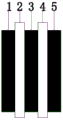
Referring to fig. 1, the bus type power board includes a first conductive layer 1, a second conductive layer 3, and a first insulating layer 2 disposed between the first conductive layer 1 and the second conductive layer 3; the printed circuit board further comprises a first power interface and at least one first power supply interface, wherein the first power interface is connected with the first conducting layer 1 and the second conducting layer 3 and used for being connected with a power supply, and for example, a +24V direct-current power supply can be provided for the board card; the first power supply interface is connected with the first conducting layer 1 and the second conducting layer 3 and used for being electrically connected with a first board card to be powered. The bus board shown in fig. 1 can carry one voltage, and the bus board in this embodiment can also be configured to carry multiple voltages. Referring to the bus type power supply board shown in fig. 2, based on the bus type power supply board shown in fig. 1, the bus type power supply board further includes a third conductive layer 5, a second insulating layer 4 disposed between the second conductive layer 3 and the third conductive layer, a second power interface, and at least one second power supply interface, where the second power interface is connected to the first conductive layer 1 and the third conductive layer 5 for accessing a power supply, for example, a-48V dc power supply may be provided for a board card; the second power supply interface is connected with the first conductive layer 1 and the third conductive layer 5 and is used for being connected with an electrical interface of a second board to be powered. It can be seen that the bussed power board shown in figure 2 can carry both +24V and-48V. Referring to fig. 3, the bus-type power board shown in the figure further includes, on the basis of the bus-type power board shown in fig. 2, a fourth conductive layer 7, a third insulating layer 6 disposed between the third conductive layer 5 and the fourth conductive layer 7, a third power interface, and at least one third power interface, where the third power interface is connected to the first conductive layer 1 and the fourth conductive layer 7 for accessing a power supply, for example, a +48V dc power supply may be provided for a board card; the third power supply interface is connected with the first conductive layer 1 and the fourth conductive layer 7 and is used for being electrically connected with a third board card to be powered. It can be seen that the bus-type power supply board shown in fig. 3 can carry three voltages of +24V, -48V and + 48V. It should be understood that when more medium voltage needs to be carried, the setting can be adjusted according to the above setting principle.
The first board card to be powered, the second board card to be powered and the third board card to be powered in the embodiment can be several types of board cards with different requirements on a power supply. It should be understood that the first power interface, the second power interface, the third power interface, and the first power interface, the second power interface, and the third power interface in this embodiment may all be disposed on one conductive layer to simplify the structural design of the bus power board, for example, all may be disposed on the first conductive layer. In addition, the first power interface, the second power interface, and the third power interface in this embodiment may select to share one power interface according to an actual application scenario, and the corresponding voltage regulation module is provided in an auxiliary manner. Of course, according to actual requirements, the first power supply interface, the second power supply interface, and the third power supply interface in this embodiment may also share the same electrical interface. The specific setting number of the power supply interfaces in this embodiment can be specifically set according to the number of boards to be powered and other conditions. It should be understood that the position, structure, and form of each power interface and each power supply interface in this embodiment may be set according to a specific application scenario, for example, the structure of each power supply interface may be specifically selected and set according to the structure of the electrical interface of the board card to be powered.
In order to further improve the reliability and safety of the power supply of the bus-type power supply board, please refer to fig. 4, the bus-type power supply board in this embodiment further includes a ground protection layer 9 and a fourth insulation layer 8 disposed between the ground protection layer 9 and the fourth conductive layer 7, and the ground protection can further improve the safety and reliability of the power supply. It should be understood that in the present embodiment, a grounding protection layer may be added on the basis of the illustration shown in fig. 1 and 2.
In this embodiment, theoretically, any conductive material, such as copper, silver, etc., can be selected for each conductive layer, and each conductive layer is preferably a copper conductive layer. That is, this embodiment preferably adopts the copper bar interval insulating layer to carry out the range upon range of design and obtains total line formula power supply board, and the copper bar function of each layer can carry out nimble setting according to the frame actual need.
The bus type power supply board in the embodiment can be directly fixed on the rack; or on a back plate inside the frame, the back plate being fixed on the frame. The specific fixing mode of the bus bar guide in this embodiment may also be selected according to a specific application scenario, such as welding, plugging, or screw fixing. When the bus type power supply board is fixed on the back board, the back board only plays a role in fixing and positioning. For example, as shown in fig. 5, backplane PCB10 has backplane signal socket 101 and positioning pin 102 for positioning the backplane PCB, an area for fixing bus power board 11 is left on top of backplane PCB10, bus power board 11 has power interface 111 and power interface 112, and fixing hole 113, and bus power board 11 is fixed on backplane PCB10 by fixing hole 113 and corresponding screw.
Referring to fig. 6, it is a schematic view of a bus-type power board made of copper bars according to the present embodiment, which can provide-48V power. Comprising an upper conductive layer 12, an intermediate insulating layer 13 in between and a lower conductive layer 14, a power supply interface 121 being arranged on one side of the upper conductive layer and a power supply interface 122 being arranged on the other side of the upper conductive layer.
It should be understood that the specific conductive material, the specific structural design, the fixing mode in the rack, and the like adopted by the bus type power supply board in the invention can be flexibly set according to specific application scenarios. According to the invention, the bus type power supply board independent of the back plate is adopted to supply power to the board card to be powered, so that compared with the existing method that the board card is supplied with power through the PCB copper sheet of the back plate, the current carrying capacity can be greatly improved, various power supply requirements can be better met, the design of the back plate is greatly simplified, the reliability of the back plate is improved, and the design, manufacturing and subsequent maintenance costs are reduced; and the bus type power supply board independent of the back board is specially used for supplying power, the specific structure of the bus type power supply board can be flexibly designed and adjusted according to the structure of the back board, the board card or the rack, and the flexibility and the reliability of power supply inside the rack can be improved.
The foregoing is a more detailed description of the present invention that is presented in conjunction with specific embodiments, and the practice of the invention is not to be considered limited to those descriptions. For those skilled in the art to which the invention pertains, several simple deductions or substitutions can be made without departing from the spirit of the invention, and all shall be considered as belonging to the protection scope of the invention.
Claims (10)
1. A bussed power board for powering inside a rack, the bussed power board being independent of a backplane inside the rack, comprising: the conductive structure comprises a first conductive layer, a second conductive layer and a first insulating layer arranged between the first conductive layer and the second conductive layer; the power supply device further comprises a first power interface and at least one first power supply interface, the first power interface is connected with the first conducting layer and the second conducting layer and used for being connected with a power supply, and the first power supply interface is connected with the first conducting layer and the second conducting layer and used for being directly connected with an electrical interface of the first board card to be powered.
2. The rack internal power bus board of claim 1, further comprising a third conductive layer, a second insulating layer disposed between the second conductive layer and the third conductive layer, a second power interface, and at least one second power interface, wherein the second power interface is connected to the first conductive layer and the third conductive layer for connecting to a power supply, and the second power interface is connected to the first conductive layer and the third conductive layer for connecting to an electrical interface of a second board to be powered.
3. The bus-type power board for supplying power inside a rack according to claim 2, further comprising a fourth conductive layer, a third insulating layer disposed between the third conductive layer and the fourth conductive layer, a third power interface and at least one third power interface, wherein the third power interface is connected with the first conductive layer and the fourth conductive layer for connecting to a power supply, and the third power interface is connected with the first conductive layer and the fourth conductive layer for connecting to an electrical interface of a third board to be powered.
4. The bussed power board of claim 3, further comprising a ground shield, a fourth insulating layer disposed between the ground shield and the fourth conductive layer.
5. The bus power board for supplying power inside a rack according to any one of claims 1 to 4, wherein the first power interface, the second power interface, the third power interface and the third power interface are all disposed on the first conductive layer.
6. A bus bar power strip for supplying power internally to a rack as claimed in any one of claims 1 to 4, wherein each of said conductive layers is a copper conductive layer.
7. A communication apparatus comprising a rack and the bus board as claimed in any one of claims 1 to 6, wherein the bus board is disposed in the rack.
8. The communication device of claim 7, further comprising a backplane fixedly disposed within the chassis, the bus power board fixedly disposed on the backplane.
9. The communication device of claim 7, wherein the bussed power board is fixedly disposed on the chassis.
10. A rack internal power supply method is characterized in that the bus type power supply board as claimed in any one of claims 1 to 6 is arranged in a rack, and a board card to be powered is connected with a power supply through the bus type power supply board to obtain power supply.
Priority Applications (1)
| Application Number | Priority Date | Filing Date | Title |
|---|---|---|---|
| CN201410811201.XA CN105789938B (en) | 2014-12-23 | 2014-12-23 | Rack internal power supply method, bus type power supply board and communication equipment |
Applications Claiming Priority (1)
| Application Number | Priority Date | Filing Date | Title |
|---|---|---|---|
| CN201410811201.XA CN105789938B (en) | 2014-12-23 | 2014-12-23 | Rack internal power supply method, bus type power supply board and communication equipment |
Publications (2)
| Publication Number | Publication Date |
|---|---|
| CN105789938A CN105789938A (en) | 2016-07-20 |
| CN105789938B true CN105789938B (en) | 2020-08-04 |
Family
ID=56377857
Family Applications (1)
| Application Number | Title | Priority Date | Filing Date |
|---|---|---|---|
| CN201410811201.XA Active CN105789938B (en) | 2014-12-23 | 2014-12-23 | Rack internal power supply method, bus type power supply board and communication equipment |
Country Status (1)
| Country | Link |
|---|---|
| CN (1) | CN105789938B (en) |
Families Citing this family (1)
| Publication number | Priority date | Publication date | Assignee | Title |
|---|---|---|---|---|
| CN114143124A (en) * | 2021-11-05 | 2022-03-04 | 国网江苏省电力有限公司盐城供电分公司 | Control device capable of starting power communication equipment in regions |
Citations (5)
| Publication number | Priority date | Publication date | Assignee | Title |
|---|---|---|---|---|
| US6255588B1 (en) * | 1998-09-08 | 2001-07-03 | International Business Machines Corporation | Arrangement for supplying power from a buss bar to a circuit board |
| CN201142332Y (en) * | 2008-01-18 | 2008-10-29 | 林健峯 | LED apparatus |
| CN101657072A (en) * | 2008-08-19 | 2010-02-24 | 富葵精密组件(深圳)有限公司 | Circuit board manufacturing method |
| CN102027605A (en) * | 2008-04-25 | 2011-04-20 | 3A技术及管理有限公司 | Device comprising a multilayer board and light-emitting diodes |
| CN102412852A (en) * | 2006-08-18 | 2012-04-11 | 德尔菲技术公司 | Lightweight audio system for automotive applications and method |
Family Cites Families (1)
| Publication number | Priority date | Publication date | Assignee | Title |
|---|---|---|---|---|
| CN203588142U (en) * | 2013-11-08 | 2014-05-07 | 华为技术有限公司 | Rack server |
-
2014
- 2014-12-23 CN CN201410811201.XA patent/CN105789938B/en active Active
Patent Citations (5)
| Publication number | Priority date | Publication date | Assignee | Title |
|---|---|---|---|---|
| US6255588B1 (en) * | 1998-09-08 | 2001-07-03 | International Business Machines Corporation | Arrangement for supplying power from a buss bar to a circuit board |
| CN102412852A (en) * | 2006-08-18 | 2012-04-11 | 德尔菲技术公司 | Lightweight audio system for automotive applications and method |
| CN201142332Y (en) * | 2008-01-18 | 2008-10-29 | 林健峯 | LED apparatus |
| CN102027605A (en) * | 2008-04-25 | 2011-04-20 | 3A技术及管理有限公司 | Device comprising a multilayer board and light-emitting diodes |
| CN101657072A (en) * | 2008-08-19 | 2010-02-24 | 富葵精密组件(深圳)有限公司 | Circuit board manufacturing method |
Also Published As
| Publication number | Publication date |
|---|---|
| CN105789938A (en) | 2016-07-20 |
Similar Documents
| Publication | Publication Date | Title |
|---|---|---|
| US20130058028A1 (en) | Server rack and power transmission assembly thereof | |
| CN103186214A (en) | Server power supply system | |
| CN105282283A (en) | Mobile terminal | |
| CN204179284U (en) | Electric connector female | |
| CN111065199A (en) | Power supply unit and veneer | |
| CN202679451U (en) | Cellphone circuit board for surface adhesion | |
| CN105789938B (en) | Rack internal power supply method, bus type power supply board and communication equipment | |
| CN104752851B (en) | A kind of system | |
| CN105100553A (en) | Camera module and electronic equipment | |
| CN103338582A (en) | Soft circuit board, and electronic device with same | |
| CN204131831U (en) | A kind of big current that prevents conducts the power panel causing local overheating | |
| CN206908946U (en) | A kind of high wiring density printed circuit board (PCB) | |
| CN203722924U (en) | Circuit board structure of electric vehicle controller | |
| CN204810680U (en) | Novel electricity daughter board | |
| CN202093449U (en) | Main board | |
| CN212366372U (en) | Power supply adapter plate of box type switch | |
| CN220438882U (en) | Power backboard and server power supply system | |
| KR20130095971A (en) | All-in-one power distribution apparatus controlling high current and communication | |
| CN102857348A (en) | Power supply system and method as well as communication equipment | |
| CN102595775B (en) | Method for arranging wires for power supply on printed circuit board and printed circuit board | |
| CN210609875U (en) | Portable satellite communication equipment control board card | |
| CN211090117U (en) | Flexible line deconcentrator with corner | |
| KR20120067654A (en) | Connector for pcb and electronic device having the same | |
| CN105025652A (en) | Novel electronic printed circuit board | |
| CN202888433U (en) | An electric appliance connecting system |
Legal Events
| Date | Code | Title | Description |
|---|---|---|---|
| C06 | Publication | ||
| PB01 | Publication | ||
| SE01 | Entry into force of request for substantive examination | ||
| SE01 | Entry into force of request for substantive examination | ||
| TA01 | Transfer of patent application right |
Effective date of registration: 20200707 Address after: 210012 Nanjing, Yuhuatai District, South Street, Bauhinia Road, No. 68 Applicant after: Nanjing Zhongxing Software Co.,Ltd. Address before: 518057 Nanshan District science and Technology Industrial Park, Guangdong high tech Industrial Park, ZTE building Applicant before: ZTE Corp. |
|
| TA01 | Transfer of patent application right | ||
| GR01 | Patent grant | ||
| GR01 | Patent grant |