CN105390448B - Method for manufacturing semiconductor device - Google Patents
Method for manufacturing semiconductor device Download PDFInfo
- Publication number
- CN105390448B CN105390448B CN201510535778.7A CN201510535778A CN105390448B CN 105390448 B CN105390448 B CN 105390448B CN 201510535778 A CN201510535778 A CN 201510535778A CN 105390448 B CN105390448 B CN 105390448B
- Authority
- CN
- China
- Prior art keywords
- region
- film
- insulating film
- gate electrode
- forming
- Prior art date
- Legal status (The legal status is an assumption and is not a legal conclusion. Google has not performed a legal analysis and makes no representation as to the accuracy of the status listed.)
- Active
Links
- 239000004065 semiconductor Substances 0.000 title claims abstract description 503
- 238000004519 manufacturing process Methods 0.000 title claims abstract description 211
- 238000000034 method Methods 0.000 title claims description 30
- 230000015654 memory Effects 0.000 claims abstract description 239
- 239000000758 substrate Substances 0.000 claims abstract description 110
- 238000005468 ion implantation Methods 0.000 claims abstract description 78
- 230000005669 field effect Effects 0.000 claims abstract description 58
- 239000004020 conductor Substances 0.000 claims abstract description 39
- 238000000059 patterning Methods 0.000 claims abstract description 37
- 229910021420 polycrystalline silicon Inorganic materials 0.000 claims description 92
- 229920005591 polysilicon Polymers 0.000 claims description 87
- 238000003860 storage Methods 0.000 claims description 73
- VYPSYNLAJGMNEJ-UHFFFAOYSA-N Silicium dioxide Chemical compound O=[Si]=O VYPSYNLAJGMNEJ-UHFFFAOYSA-N 0.000 claims description 49
- 229910052814 silicon oxide Inorganic materials 0.000 claims description 48
- 239000012535 impurity Substances 0.000 claims description 27
- 229910052581 Si3N4 Inorganic materials 0.000 claims description 19
- HQVNEWCFYHHQES-UHFFFAOYSA-N silicon nitride Chemical compound N12[Si]34N5[Si]62N3[Si]51N64 HQVNEWCFYHHQES-UHFFFAOYSA-N 0.000 claims description 19
- 238000001039 wet etching Methods 0.000 claims description 12
- NBIIXXVUZAFLBC-UHFFFAOYSA-N Phosphoric acid Chemical compound OP(O)(O)=O NBIIXXVUZAFLBC-UHFFFAOYSA-N 0.000 claims description 8
- 125000006850 spacer group Chemical group 0.000 claims description 7
- 238000009966 trimming Methods 0.000 claims description 7
- 229910000147 aluminium phosphate Inorganic materials 0.000 claims description 4
- 230000001590 oxidative effect Effects 0.000 claims 2
- 230000003915 cell function Effects 0.000 claims 1
- 230000002829 reductive effect Effects 0.000 abstract description 18
- 239000010408 film Substances 0.000 description 620
- 230000015572 biosynthetic process Effects 0.000 description 301
- LPQOADBMXVRBNX-UHFFFAOYSA-N ac1ldcw0 Chemical compound Cl.C1CN(C)CCN1C1=C(F)C=C2C(=O)C(C(O)=O)=CN3CCSC1=C32 LPQOADBMXVRBNX-UHFFFAOYSA-N 0.000 description 198
- 230000015556 catabolic process Effects 0.000 description 135
- 239000010410 layer Substances 0.000 description 44
- 238000011068 loading method Methods 0.000 description 43
- XUIMIQQOPSSXEZ-UHFFFAOYSA-N Silicon Chemical compound [Si] XUIMIQQOPSSXEZ-UHFFFAOYSA-N 0.000 description 33
- 229910052710 silicon Inorganic materials 0.000 description 33
- 239000010703 silicon Substances 0.000 description 33
- 238000000206 photolithography Methods 0.000 description 32
- 238000002955 isolation Methods 0.000 description 31
- 239000011248 coating agent Substances 0.000 description 27
- 238000000576 coating method Methods 0.000 description 27
- 239000000470 constituent Substances 0.000 description 25
- 102100038837 2-Hydroxyacid oxidase 1 Human genes 0.000 description 20
- 101001015570 Arabidopsis thaliana Glycolate oxidase 1 Proteins 0.000 description 20
- 101001031589 Homo sapiens 2-Hydroxyacid oxidase 1 Proteins 0.000 description 20
- 101000887873 Arabidopsis thaliana Glycolate oxidase 2 Proteins 0.000 description 18
- 238000005530 etching Methods 0.000 description 18
- 239000011229 interlayer Substances 0.000 description 18
- 230000004048 modification Effects 0.000 description 15
- 238000012986 modification Methods 0.000 description 15
- 230000009467 reduction Effects 0.000 description 15
- 241000839426 Chlamydia virus Chp1 Species 0.000 description 14
- 101000945096 Homo sapiens Ribosomal protein S6 kinase alpha-5 Proteins 0.000 description 14
- 102100033645 Ribosomal protein S6 kinase alpha-5 Human genes 0.000 description 14
- 229910021332 silicide Inorganic materials 0.000 description 13
- FVBUAEGBCNSCDD-UHFFFAOYSA-N silicide(4-) Chemical compound [Si-4] FVBUAEGBCNSCDD-UHFFFAOYSA-N 0.000 description 13
- PCLURTMBFDTLSK-UHFFFAOYSA-N nickel platinum Chemical compound [Ni].[Pt] PCLURTMBFDTLSK-UHFFFAOYSA-N 0.000 description 12
- 230000000694 effects Effects 0.000 description 11
- 230000008569 process Effects 0.000 description 11
- JPKJQBJPBRLVTM-OSLIGDBKSA-N (2s)-2-amino-n-[(2s,3r)-3-hydroxy-1-[[(2s)-1-[[(2s)-1-[[(2s)-1-[[(2r)-1-(1h-indol-3-yl)-3-oxopropan-2-yl]amino]-1-oxo-3-phenylpropan-2-yl]amino]-1-oxo-3-phenylpropan-2-yl]amino]-1-oxo-3-phenylpropan-2-yl]amino]-1-oxobutan-2-yl]-6-iminohexanamide Chemical compound C([C@H](NC(=O)[C@@H](NC(=O)[C@@H](N)CCCC=N)[C@H](O)C)C(=O)N[C@@H](CC=1C=CC=CC=1)C(=O)N[C@@H](CC=1C=CC=CC=1)C(=O)N[C@H](CC=1C2=CC=CC=C2NC=1)C=O)C1=CC=CC=C1 JPKJQBJPBRLVTM-OSLIGDBKSA-N 0.000 description 10
- 102100031277 Calcineurin B homologous protein 1 Human genes 0.000 description 10
- 101000777252 Homo sapiens Calcineurin B homologous protein 1 Proteins 0.000 description 10
- 101000943802 Homo sapiens Cysteine and histidine-rich domain-containing protein 1 Proteins 0.000 description 10
- 238000001312 dry etching Methods 0.000 description 9
- 230000006870 function Effects 0.000 description 8
- 229910021339 platinum silicide Inorganic materials 0.000 description 8
- 241000080590 Niso Species 0.000 description 7
- NRTOMJZYCJJWKI-UHFFFAOYSA-N Titanium nitride Chemical compound [Ti]#N NRTOMJZYCJJWKI-UHFFFAOYSA-N 0.000 description 7
- 238000009792 diffusion process Methods 0.000 description 7
- 239000010936 titanium Substances 0.000 description 7
- 229910052719 titanium Inorganic materials 0.000 description 7
- RTAQQCXQSZGOHL-UHFFFAOYSA-N Titanium Chemical compound [Ti] RTAQQCXQSZGOHL-UHFFFAOYSA-N 0.000 description 6
- 230000004888 barrier function Effects 0.000 description 6
- 238000007667 floating Methods 0.000 description 6
- 230000002093 peripheral effect Effects 0.000 description 6
- RYGMFSIKBFXOCR-UHFFFAOYSA-N Copper Chemical compound [Cu] RYGMFSIKBFXOCR-UHFFFAOYSA-N 0.000 description 5
- 108010063256 HTLV-1 protease Proteins 0.000 description 5
- 101000945093 Homo sapiens Ribosomal protein S6 kinase alpha-4 Proteins 0.000 description 5
- 101000900567 Pisum sativum Disease resistance response protein Pi49 Proteins 0.000 description 5
- 101000621511 Potato virus M (strain German) RNA silencing suppressor Proteins 0.000 description 5
- 102100033644 Ribosomal protein S6 kinase alpha-4 Human genes 0.000 description 5
- 229910052802 copper Inorganic materials 0.000 description 5
- 239000010949 copper Substances 0.000 description 5
- 238000009413 insulation Methods 0.000 description 5
- 238000004544 sputter deposition Methods 0.000 description 5
- 102100031272 Calcineurin B homologous protein 2 Human genes 0.000 description 4
- 102100031077 Calcineurin B homologous protein 3 Human genes 0.000 description 4
- 241001510512 Chlamydia phage 2 Species 0.000 description 4
- KRHYYFGTRYWZRS-UHFFFAOYSA-N Fluorane Chemical compound F KRHYYFGTRYWZRS-UHFFFAOYSA-N 0.000 description 4
- 101710131019 Glycolate oxidase 2 Proteins 0.000 description 4
- 101000777239 Homo sapiens Calcineurin B homologous protein 2 Proteins 0.000 description 4
- 101000777270 Homo sapiens Calcineurin B homologous protein 3 Proteins 0.000 description 4
- OAICVXFJPJFONN-UHFFFAOYSA-N Phosphorus Chemical compound [P] OAICVXFJPJFONN-UHFFFAOYSA-N 0.000 description 4
- 229910052785 arsenic Inorganic materials 0.000 description 4
- RQNWIZPPADIBDY-UHFFFAOYSA-N arsenic atom Chemical compound [As] RQNWIZPPADIBDY-UHFFFAOYSA-N 0.000 description 4
- 230000008901 benefit Effects 0.000 description 4
- 230000006872 improvement Effects 0.000 description 4
- 230000000149 penetrating effect Effects 0.000 description 4
- 229910052698 phosphorus Inorganic materials 0.000 description 4
- 239000011574 phosphorus Substances 0.000 description 4
- WFKWXMTUELFFGS-UHFFFAOYSA-N tungsten Chemical compound [W] WFKWXMTUELFFGS-UHFFFAOYSA-N 0.000 description 4
- 229910052721 tungsten Inorganic materials 0.000 description 4
- 239000010937 tungsten Substances 0.000 description 4
- 229910052782 aluminium Inorganic materials 0.000 description 3
- XAGFODPZIPBFFR-UHFFFAOYSA-N aluminium Chemical compound [Al] XAGFODPZIPBFFR-UHFFFAOYSA-N 0.000 description 3
- 238000006243 chemical reaction Methods 0.000 description 3
- 239000013078 crystal Substances 0.000 description 3
- 238000010586 diagram Methods 0.000 description 3
- 238000002513 implantation Methods 0.000 description 3
- 239000012212 insulator Substances 0.000 description 3
- 230000014759 maintenance of location Effects 0.000 description 3
- 230000003647 oxidation Effects 0.000 description 3
- 238000007254 oxidation reaction Methods 0.000 description 3
- 230000003068 static effect Effects 0.000 description 3
- 229910052715 tantalum Inorganic materials 0.000 description 3
- GUVRBAGPIYLISA-UHFFFAOYSA-N tantalum atom Chemical compound [Ta] GUVRBAGPIYLISA-UHFFFAOYSA-N 0.000 description 3
- MZLGASXMSKOWSE-UHFFFAOYSA-N tantalum nitride Chemical compound [Ta]#N MZLGASXMSKOWSE-UHFFFAOYSA-N 0.000 description 3
- ZOXJGFHDIHLPTG-UHFFFAOYSA-N Boron Chemical compound [B] ZOXJGFHDIHLPTG-UHFFFAOYSA-N 0.000 description 2
- 241000293849 Cordylanthus Species 0.000 description 2
- 101710131017 Glycolate oxidase 1 Proteins 0.000 description 2
- 210000000746 body region Anatomy 0.000 description 2
- 229910052796 boron Inorganic materials 0.000 description 2
- 238000011109 contamination Methods 0.000 description 2
- 238000013500 data storage Methods 0.000 description 2
- 230000007547 defect Effects 0.000 description 2
- 150000002500 ions Chemical class 0.000 description 2
- 238000002156 mixing Methods 0.000 description 2
- 238000005498 polishing Methods 0.000 description 2
- 239000000126 substance Substances 0.000 description 2
- ZXEYZECDXFPJRJ-UHFFFAOYSA-N $l^{3}-silane;platinum Chemical compound [SiH3].[Pt] ZXEYZECDXFPJRJ-UHFFFAOYSA-N 0.000 description 1
- 230000005689 Fowler Nordheim tunneling Effects 0.000 description 1
- 101100049574 Human herpesvirus 6A (strain Uganda-1102) U5 gene Proteins 0.000 description 1
- UFHFLCQGNIYNRP-UHFFFAOYSA-N Hydrogen Chemical compound [H][H] UFHFLCQGNIYNRP-UHFFFAOYSA-N 0.000 description 1
- 230000002159 abnormal effect Effects 0.000 description 1
- 230000009471 action Effects 0.000 description 1
- 239000000853 adhesive Substances 0.000 description 1
- 230000001070 adhesive effect Effects 0.000 description 1
- 238000000137 annealing Methods 0.000 description 1
- 230000008859 change Effects 0.000 description 1
- 229910017052 cobalt Inorganic materials 0.000 description 1
- 239000010941 cobalt Substances 0.000 description 1
- GUTLYIVDDKVIGB-UHFFFAOYSA-N cobalt atom Chemical compound [Co] GUTLYIVDDKVIGB-UHFFFAOYSA-N 0.000 description 1
- 238000010276 construction Methods 0.000 description 1
- 230000007423 decrease Effects 0.000 description 1
- 230000003247 decreasing effect Effects 0.000 description 1
- 230000005684 electric field Effects 0.000 description 1
- 238000009713 electroplating Methods 0.000 description 1
- 238000005516 engineering process Methods 0.000 description 1
- 230000001747 exhibiting effect Effects 0.000 description 1
- 238000011049 filling Methods 0.000 description 1
- 238000010438 heat treatment Methods 0.000 description 1
- 239000002784 hot electron Substances 0.000 description 1
- 229910052739 hydrogen Inorganic materials 0.000 description 1
- 239000001257 hydrogen Substances 0.000 description 1
- 201000006747 infectious mononucleosis Diseases 0.000 description 1
- 230000010354 integration Effects 0.000 description 1
- 239000004973 liquid crystal related substance Substances 0.000 description 1
- 239000000463 material Substances 0.000 description 1
- 239000011159 matrix material Substances 0.000 description 1
- 229910052751 metal Inorganic materials 0.000 description 1
- 239000002184 metal Substances 0.000 description 1
- -1 metal Oxide Nitride Chemical class 0.000 description 1
- 229910044991 metal oxide Inorganic materials 0.000 description 1
- 229910021334 nickel silicide Inorganic materials 0.000 description 1
- RUFLMLWJRZAWLJ-UHFFFAOYSA-N nickel silicide Chemical compound [Ni]=[Si]=[Ni] RUFLMLWJRZAWLJ-UHFFFAOYSA-N 0.000 description 1
- 238000005457 optimization Methods 0.000 description 1
- 230000000717 retained effect Effects 0.000 description 1
- 101150064834 ssl1 gene Proteins 0.000 description 1
- 230000002195 synergetic effect Effects 0.000 description 1
- 239000010409 thin film Substances 0.000 description 1
- 230000036962 time dependent Effects 0.000 description 1
- 150000003608 titanium Chemical class 0.000 description 1
- 229910021341 titanium silicide Inorganic materials 0.000 description 1
- 230000005641 tunneling Effects 0.000 description 1
Images


Classifications
-
- H—ELECTRICITY
- H10—SEMICONDUCTOR DEVICES; ELECTRIC SOLID-STATE DEVICES NOT OTHERWISE PROVIDED FOR
- H10B—ELECTRONIC MEMORY DEVICES
- H10B69/00—Erasable-and-programmable ROM [EPROM] devices not provided for in groups H10B41/00 - H10B63/00, e.g. ultraviolet erasable-and-programmable ROM [UVEPROM] devices
-
- H—ELECTRICITY
- H01—ELECTRIC ELEMENTS
- H01L—SEMICONDUCTOR DEVICES NOT COVERED BY CLASS H10
- H01L29/00—Semiconductor devices specially adapted for rectifying, amplifying, oscillating or switching and having potential barriers; Capacitors or resistors having potential barriers, e.g. a PN-junction depletion layer or carrier concentration layer; Details of semiconductor bodies or of electrodes thereof ; Multistep manufacturing processes therefor
- H01L29/66—Types of semiconductor device ; Multistep manufacturing processes therefor
- H01L29/66007—Multistep manufacturing processes
- H01L29/66075—Multistep manufacturing processes of devices having semiconductor bodies comprising group 14 or group 13/15 materials
- H01L29/66227—Multistep manufacturing processes of devices having semiconductor bodies comprising group 14 or group 13/15 materials the devices being controllable only by the electric current supplied or the electric potential applied, to an electrode which does not carry the current to be rectified, amplified or switched, e.g. three-terminal devices
- H01L29/66409—Unipolar field-effect transistors
- H01L29/66477—Unipolar field-effect transistors with an insulated gate, i.e. MISFET
- H01L29/66833—Unipolar field-effect transistors with an insulated gate, i.e. MISFET with a charge trapping gate insulator, e.g. MNOS transistors
-
- H—ELECTRICITY
- H10—SEMICONDUCTOR DEVICES; ELECTRIC SOLID-STATE DEVICES NOT OTHERWISE PROVIDED FOR
- H10B—ELECTRONIC MEMORY DEVICES
- H10B43/00—EEPROM devices comprising charge-trapping gate insulators
- H10B43/50—EEPROM devices comprising charge-trapping gate insulators characterised by the boundary region between the core and peripheral circuit regions
-
- H—ELECTRICITY
- H01—ELECTRIC ELEMENTS
- H01L—SEMICONDUCTOR DEVICES NOT COVERED BY CLASS H10
- H01L21/00—Processes or apparatus adapted for the manufacture or treatment of semiconductor or solid state devices or of parts thereof
- H01L21/02—Manufacture or treatment of semiconductor devices or of parts thereof
- H01L21/04—Manufacture or treatment of semiconductor devices or of parts thereof the devices having potential barriers, e.g. a PN junction, depletion layer or carrier concentration layer
- H01L21/18—Manufacture or treatment of semiconductor devices or of parts thereof the devices having potential barriers, e.g. a PN junction, depletion layer or carrier concentration layer the devices having semiconductor bodies comprising elements of Group IV of the Periodic Table or AIIIBV compounds with or without impurities, e.g. doping materials
- H01L21/26—Bombardment with radiation
- H01L21/263—Bombardment with radiation with high-energy radiation
- H01L21/265—Bombardment with radiation with high-energy radiation producing ion implantation
- H01L21/266—Bombardment with radiation with high-energy radiation producing ion implantation using masks
-
- H—ELECTRICITY
- H01—ELECTRIC ELEMENTS
- H01L—SEMICONDUCTOR DEVICES NOT COVERED BY CLASS H10
- H01L21/00—Processes or apparatus adapted for the manufacture or treatment of semiconductor or solid state devices or of parts thereof
- H01L21/02—Manufacture or treatment of semiconductor devices or of parts thereof
- H01L21/04—Manufacture or treatment of semiconductor devices or of parts thereof the devices having potential barriers, e.g. a PN junction, depletion layer or carrier concentration layer
- H01L21/18—Manufacture or treatment of semiconductor devices or of parts thereof the devices having potential barriers, e.g. a PN junction, depletion layer or carrier concentration layer the devices having semiconductor bodies comprising elements of Group IV of the Periodic Table or AIIIBV compounds with or without impurities, e.g. doping materials
- H01L21/28—Manufacture of electrodes on semiconductor bodies using processes or apparatus not provided for in groups H01L21/20 - H01L21/268
- H01L21/28008—Making conductor-insulator-semiconductor electrodes
-
- H—ELECTRICITY
- H01—ELECTRIC ELEMENTS
- H01L—SEMICONDUCTOR DEVICES NOT COVERED BY CLASS H10
- H01L21/00—Processes or apparatus adapted for the manufacture or treatment of semiconductor or solid state devices or of parts thereof
- H01L21/02—Manufacture or treatment of semiconductor devices or of parts thereof
- H01L21/04—Manufacture or treatment of semiconductor devices or of parts thereof the devices having potential barriers, e.g. a PN junction, depletion layer or carrier concentration layer
- H01L21/18—Manufacture or treatment of semiconductor devices or of parts thereof the devices having potential barriers, e.g. a PN junction, depletion layer or carrier concentration layer the devices having semiconductor bodies comprising elements of Group IV of the Periodic Table or AIIIBV compounds with or without impurities, e.g. doping materials
- H01L21/30—Treatment of semiconductor bodies using processes or apparatus not provided for in groups H01L21/20 - H01L21/26
- H01L21/31—Treatment of semiconductor bodies using processes or apparatus not provided for in groups H01L21/20 - H01L21/26 to form insulating layers thereon, e.g. for masking or by using photolithographic techniques; After treatment of these layers; Selection of materials for these layers
- H01L21/3105—After-treatment
- H01L21/311—Etching the insulating layers by chemical or physical means
- H01L21/31105—Etching inorganic layers
- H01L21/31111—Etching inorganic layers by chemical means
- H01L21/31116—Etching inorganic layers by chemical means by dry-etching
-
- H—ELECTRICITY
- H01—ELECTRIC ELEMENTS
- H01L—SEMICONDUCTOR DEVICES NOT COVERED BY CLASS H10
- H01L23/00—Details of semiconductor or other solid state devices
- H01L23/52—Arrangements for conducting electric current within the device in operation from one component to another, i.e. interconnections, e.g. wires, lead frames
- H01L23/522—Arrangements for conducting electric current within the device in operation from one component to another, i.e. interconnections, e.g. wires, lead frames including external interconnections consisting of a multilayer structure of conductive and insulating layers inseparably formed on the semiconductor body
- H01L23/525—Arrangements for conducting electric current within the device in operation from one component to another, i.e. interconnections, e.g. wires, lead frames including external interconnections consisting of a multilayer structure of conductive and insulating layers inseparably formed on the semiconductor body with adaptable interconnections
- H01L23/5256—Arrangements for conducting electric current within the device in operation from one component to another, i.e. interconnections, e.g. wires, lead frames including external interconnections consisting of a multilayer structure of conductive and insulating layers inseparably formed on the semiconductor body with adaptable interconnections comprising fuses, i.e. connections having their state changed from conductive to non-conductive
-
- H—ELECTRICITY
- H10—SEMICONDUCTOR DEVICES; ELECTRIC SOLID-STATE DEVICES NOT OTHERWISE PROVIDED FOR
- H10B—ELECTRONIC MEMORY DEVICES
- H10B20/00—Read-only memory [ROM] devices
- H10B20/20—Programmable ROM [PROM] devices comprising field-effect components
-
- H—ELECTRICITY
- H10—SEMICONDUCTOR DEVICES; ELECTRIC SOLID-STATE DEVICES NOT OTHERWISE PROVIDED FOR
- H10B—ELECTRONIC MEMORY DEVICES
- H10B43/00—EEPROM devices comprising charge-trapping gate insulators
- H10B43/30—EEPROM devices comprising charge-trapping gate insulators characterised by the memory core region
- H10B43/35—EEPROM devices comprising charge-trapping gate insulators characterised by the memory core region with cell select transistors, e.g. NAND
-
- H—ELECTRICITY
- H10—SEMICONDUCTOR DEVICES; ELECTRIC SOLID-STATE DEVICES NOT OTHERWISE PROVIDED FOR
- H10B—ELECTRONIC MEMORY DEVICES
- H10B43/00—EEPROM devices comprising charge-trapping gate insulators
- H10B43/40—EEPROM devices comprising charge-trapping gate insulators characterised by the peripheral circuit region
-
- H—ELECTRICITY
- H01—ELECTRIC ELEMENTS
- H01L—SEMICONDUCTOR DEVICES NOT COVERED BY CLASS H10
- H01L21/00—Processes or apparatus adapted for the manufacture or treatment of semiconductor or solid state devices or of parts thereof
- H01L21/02—Manufacture or treatment of semiconductor devices or of parts thereof
- H01L21/04—Manufacture or treatment of semiconductor devices or of parts thereof the devices having potential barriers, e.g. a PN junction, depletion layer or carrier concentration layer
- H01L21/18—Manufacture or treatment of semiconductor devices or of parts thereof the devices having potential barriers, e.g. a PN junction, depletion layer or carrier concentration layer the devices having semiconductor bodies comprising elements of Group IV of the Periodic Table or AIIIBV compounds with or without impurities, e.g. doping materials
- H01L21/26—Bombardment with radiation
- H01L21/263—Bombardment with radiation with high-energy radiation
- H01L21/265—Bombardment with radiation with high-energy radiation producing ion implantation
- H01L21/26506—Bombardment with radiation with high-energy radiation producing ion implantation in group IV semiconductors
- H01L21/26513—Bombardment with radiation with high-energy radiation producing ion implantation in group IV semiconductors of electrically active species
Landscapes
- Engineering & Computer Science (AREA)
- Physics & Mathematics (AREA)
- Microelectronics & Electronic Packaging (AREA)
- Power Engineering (AREA)
- Computer Hardware Design (AREA)
- General Physics & Mathematics (AREA)
- Condensed Matter Physics & Semiconductors (AREA)
- Manufacturing & Machinery (AREA)
- Chemical & Material Sciences (AREA)
- High Energy & Nuclear Physics (AREA)
- Toxicology (AREA)
- Health & Medical Sciences (AREA)
- Chemical Kinetics & Catalysis (AREA)
- General Chemical & Material Sciences (AREA)
- Inorganic Chemistry (AREA)
- Ceramic Engineering (AREA)
- Semiconductor Memories (AREA)
- Non-Volatile Memory (AREA)
- Metal-Oxide And Bipolar Metal-Oxide Semiconductor Integrated Circuits (AREA)
Abstract
The present invention relates to a method of manufacturing a semiconductor device. To provide a semiconductor device in which a nonvolatile memory cell and a field effect transistor are mixedly loaded at a reduced cost. The method of manufacturing a semiconductor device includes: forming n of a nonvolatile memory cell in a semiconductor substrate by ion implantation by patterning a conductor film using an additional mask covering a gate electrode forming region of a memory forming region and exposing a main circuit forming region, i.e., a field effect transistor forming region, and thereby forming a gate electrode of the nonvolatile memory cell in the memory forming region, and then using the above additional mask without changing it to another‑A type semiconductor region.
Description
CROSS-REFERENCE TO RELATED APPLICATIONS
The disclosure of japanese patent application No.2014-172680, including the specification, drawings and abstract, filed on day 27/8/2014 is incorporated herein in its entirety by this reference.
Technical Field
The present invention relates to a manufacturing technique of a semiconductor device, and for example, to a technique effective when applied to a manufacturing technique of a semiconductor device having a main circuit including a field effect transistor and a nonvolatile memory as an additional circuit.
Background
Japanese unexamined patent application publication No.2007-234861 (patent document 1) describes a technique of manufacturing a semiconductor device by forming a gate electrode of a field-effect transistor and a gate electrode of a nonvolatile memory cell, which may have improved reliability, by different steps, respectively.
[ patent document 1] Japanese unexamined patent application publication No.2007-
Disclosure of Invention
A semiconductor device having a main circuit including a field-effect transistor sometimes has an additional circuit (additional circuit) added to the main circuit in addition to the main circuit for realizing the main function of the semiconductor device. Examples of the addition circuit include an electric fuse to be used for trimming or releasing of the main circuit and a memory for storing trimming information.
At present, one of the most popular electric fuses is an otp (one Time program) type electric fuse, which is implemented by applying a large current to a polysilicon film to physically blow it out [0]/[1 ]. In recent years, there has been an increasing demand for an mtp (multi Time program) -type electric fuse that can be repeatedly adjusted by using a rewritable nonvolatile memory.
Now, as a memory for storing trimming information, a nonvolatile memory (NV memory) having a floating gate structure and suitable for hybrid loading with a field effect transistor included in a main circuit is employed. Since the use of such a nonvolatile memory increases the size of the memory cell, a shift to a nonvolatile memory capable of miniaturizing the memory cell is under study.
Under such circumstances, studies have been made on a nonvolatile memory using a monos (metal Oxide Nitride Oxide semiconductor) structure as an additional circuit. When using the nonvolatile memory having the MONOS structure as the additional circuit, the manufacturing steps of the nonvolatile memory having the MONOS structure should be incorporated in the manufacturing steps of the main circuit including the field-effect transistor. This may increase the manufacturing cost of the semiconductor device. More specifically, the mixed loading of the nonvolatile memory having the MONOS structure and the field effect transistor of the main circuit increases the number of masks. There is therefore a need to reduce the number of masks to be added and thereby reduce the manufacturing cost of semiconductor devices.
Another problem and novel features will become apparent from the description and drawings herein.
In a method of manufacturing a semiconductor device according to one embodiment, a gate electrode of a nonvolatile memory cell is formed in a memory formation region by patterning a conductor film with a mask that covers a gate electrode formation region of the memory formation region and exposes a MISFET formation region (field effect transistor formation region); and then, n of the nonvolatile memory cell is formed in the semiconductor substrate by ion implantation using the above mask without changing it to another one-A type semiconductor region.
In a method of manufacturing a semiconductor device according to another embodiment, a memory formation region is formed by using a gate electrode covering the memory formation regionAnd exposing the mask of the MISFET forming region to pattern the conductor film to form a gate electrode of the nonvolatile memory cell in the memory forming region; and then forming n of the nonvolatile memory cell in the semiconductor substrate by ion implantation using the gate electrode of the nonvolatile memory cell exposed by removing the above mask as a mask-A type semiconductor region.
According to the above-described embodiments, a semiconductor device having both a nonvolatile memory cell and a field effect transistor can be manufactured at reduced cost.
Drawings
Fig. 1 shows a layout configuration example of a semiconductor chip of the first embodiment;
fig. 2 shows an example of a circuit block configuration of a nonvolatile memory;
fig. 3 is a sectional view showing an example of the device structure of the semiconductor chip of the first embodiment;
FIG. 4 is an explanatory diagram showing one example of a memory array structure and operating conditions of the nonvolatile memory;
fig. 5 is a flowchart showing a flow of manufacturing steps of a semiconductor device in the related art;
fig. 6 is a flowchart showing a flow of manufacturing steps of the semiconductor device of the first embodiment;
fig. 7 is a sectional view showing the manufacturing step of the semiconductor device of the first embodiment;
fig. 8 is a sectional view showing a manufacturing step of the semiconductor device after the manufacturing step of fig. 7;
fig. 9 is a sectional view showing a manufacturing step of the semiconductor device after the manufacturing step of fig. 8;
fig. 10 is a sectional view showing a manufacturing step of the semiconductor device after the manufacturing step of fig. 9;
fig. 11 is a sectional view showing a manufacturing step of the semiconductor device after the manufacturing step of fig. 10;
fig. 12 is a sectional view showing a manufacturing step of the semiconductor device after the manufacturing step of fig. 11;
fig. 13 is a sectional view showing a manufacturing step of the semiconductor device after the manufacturing step of fig. 12;
fig. 14 is a sectional view showing a manufacturing step of the semiconductor device after the manufacturing step of fig. 13;
fig. 15 is a sectional view showing a manufacturing step of the semiconductor device after the manufacturing step of fig. 14;
fig. 16 is a sectional view showing a manufacturing step of the semiconductor device after the manufacturing step of fig. 15;
fig. 17 is a sectional view showing a manufacturing step of the semiconductor device after the manufacturing step of fig. 16;
fig. 18 is a sectional view showing a manufacturing step of the semiconductor device after the manufacturing step of fig. 17;
fig. 19 is a sectional view showing a manufacturing step of the semiconductor device after the manufacturing step of fig. 18;
fig. 20 is a sectional view showing a manufacturing step of the semiconductor device after the manufacturing step of fig. 19;
fig. 21A shows a residue pattern formed in the boundary region in the first embodiment, and fig. 21B shows a technique of leaving a resist film in the boundary region and intentionally forming a large residue pattern;
fig. 22 is a sectional view showing a manufacturing step of the semiconductor device of modification example 1;
fig. 23 is a sectional view showing a manufacturing step of the semiconductor device after the manufacturing step of fig. 22;
fig. 24 is a sectional view showing a manufacturing step of the semiconductor device after the manufacturing step of fig. 23;
fig. 25 is a sectional view showing a manufacturing step of the semiconductor device of modification example 2;
fig. 26 is a sectional view showing a manufacturing step of the semiconductor device after the manufacturing step of fig. 25;
fig. 27 is a sectional view showing a manufacturing step of the semiconductor device after the manufacturing step of fig. 26;
fig. 28 is a sectional view showing a manufacturing step of the semiconductor device after the manufacturing step of fig. 27;
fig. 29 is a sectional view showing a manufacturing step of the semiconductor device of modification example 3;
fig. 30 is a sectional view showing a manufacturing step of the semiconductor device after the manufacturing step of fig. 29;
fig. 31 is a sectional view showing a manufacturing step of the semiconductor device after the manufacturing step of fig. 30;
fig. 32 is a sectional view showing a manufacturing step of the semiconductor device after the manufacturing step of fig. 31;
fig. 33 shows a layout configuration example of the semiconductor chip of the second embodiment;
fig. 34 shows a device configuration example of the semiconductor chip of the second embodiment;
fig. 35 is a sectional view showing the manufacturing step of the semiconductor device of the second embodiment;
fig. 36 is a sectional view showing a manufacturing step of the semiconductor device after the manufacturing step of fig. 35;
fig. 37 is a sectional view showing a manufacturing step of the semiconductor device after the manufacturing step of fig. 36;
fig. 38 is a sectional view showing a manufacturing step of the semiconductor device after the manufacturing step of fig. 37;
fig. 39 is a sectional view showing the manufacturing step of the semiconductor device after the manufacturing step of fig. 38;
fig. 40 is a sectional view showing a manufacturing step of the semiconductor device after the manufacturing step of fig. 39;
fig. 41 is a sectional view showing a manufacturing step of the semiconductor device after the manufacturing step of fig. 40;
fig. 42 is a sectional view showing a manufacturing step of the semiconductor device after the manufacturing step of fig. 41;
fig. 43 is a sectional view showing a manufacturing step of the semiconductor device after the manufacturing step of fig. 42;
fig. 44 is a sectional view showing a manufacturing step of the semiconductor device after the manufacturing step of fig. 43;
fig. 45 is a sectional view showing a manufacturing step of the semiconductor device after the manufacturing step of fig. 44;
fig. 46 is a sectional view showing a manufacturing step of the semiconductor device after the manufacturing step of fig. 45;
fig. 47 is a sectional view showing a manufacturing step of the semiconductor device after the manufacturing step of fig. 46;
fig. 48 shows a device configuration example of the semiconductor chip of the third embodiment;
fig. 49 is a flowchart showing a flow of manufacturing steps of a semiconductor device in the related art;
fig. 50 is a flowchart showing a flow of manufacturing steps of the semiconductor device of the third embodiment;
fig. 51 is a sectional view showing the manufacturing step of the semiconductor device of the third embodiment;
fig. 52 is a sectional view showing a manufacturing step of the semiconductor device after the manufacturing step of fig. 51;
fig. 53 is a sectional view showing a manufacturing step of the semiconductor device after the manufacturing step of fig. 52;
fig. 54 is a sectional view showing a manufacturing step of the semiconductor device after the manufacturing step of fig. 53;
fig. 55 is a sectional view showing a manufacturing step of the semiconductor device after the manufacturing step of fig. 54;
fig. 56 is a sectional view showing a manufacturing step of the semiconductor device after the manufacturing step of fig. 55;
fig. 57 is a sectional view showing a manufacturing step of the semiconductor device after the manufacturing step of fig. 56;
fig. 58 is a sectional view showing a manufacturing step of the semiconductor device after the manufacturing step of fig. 57;
fig. 59 is a sectional view showing a manufacturing step of the semiconductor device after the manufacturing step of fig. 58;
fig. 60 is a sectional view showing a manufacturing step of the semiconductor device after the manufacturing step of fig. 59;
fig. 61 is a sectional view showing a manufacturing step of the semiconductor device after the manufacturing step of fig. 60;
fig. 62 is a sectional view showing a manufacturing step of the semiconductor device after the manufacturing step of fig. 61;
fig. 63 is a sectional view showing a manufacturing step of the semiconductor device after the manufacturing step of fig. 62;
fig. 64 is a sectional view showing a manufacturing step of the semiconductor device of the modification example;
fig. 65 is a sectional view showing a manufacturing step of the semiconductor device after the manufacturing step of fig. 64; and
fig. 66 is a sectional view showing a manufacturing step of the semiconductor device after the manufacturing step of fig. 65.
In the following embodiments, if necessary for convenience, the description may be made after dividing the description into a plurality of parts or embodiments. Unless otherwise specifically indicated, these parts or embodiments are not independent of each other, but one of them may be a part of or an entire modified example, detailed description, supplementary description, or the like of the other.
In the following embodiments, when referring to a number of elements (including numbers, values, amounts, ranges, etc.), unless otherwise specifically stated or generally apparent that the number is limited to a particular number, the number is not limited to the particular number, but may be greater or less than the particular number.
Further, needless to say, in the following embodiments, constituent components (including constituent steps and the like) are not necessarily indispensable unless otherwise specifically indicated or generally obvious.
Also, in the following embodiments, when referring to the shape, positional relationship, and the like of the constituent elements, the shape, positional relationship, and the like substantially close to or similar to the shape, positional relationship, and the like are also included unless otherwise specifically indicated or substantially obvious. This also applies to the numbers or ranges mentioned above.
In all the drawings for explaining the embodiments, components having the same functions will be identified by the same reference numerals and repeated explanation will be omitted. Shading may even be used on the plan view to facilitate its understanding.
Detailed Description
(first embodiment)
The technical idea in the first embodiment is a technical idea regarding a semiconductor device having, in one semiconductor chip, a main circuit for realizing a main function of the semiconductor chip and an additional circuit to be added to the main circuit and referred to as an "additional circuit", and having a MONOS type rewritable nonvolatile memory as the additional circuit.
For example, an SOC (system on chip) has, as a main circuit, a memory circuit such as a DRAM (dynamic random access memory) or an SRAM (static random access memory), a logic circuit such as a CPU (central processing unit) or an MPU (micro processing unit), or a hybrid circuit of such a memory circuit and a logic circuit. On the other hand, examples of the additional circuit include a storage circuit for storing relatively small-capacity information related to the main circuit and an electric fuse to be used for release of the circuit. Examples of the relatively small-capacity information include positional address information of an element to be used for trimming in a semiconductor chip, positional address information of a released memory cell to be used for a memory circuit, and a product number of a semiconductor device. When the semiconductor chip is an LCD (liquid crystal display) driver, examples of the relatively small-capacity information include trimming branch information of an adjustment voltage to be used for LCD image adjustment.
< example of layout configuration of semiconductor chip >
The first embodiment will be explained next using a semiconductor chip having a system for realizing a main function as an example. The semiconductor chip in the first embodiment includes therein a low breakdown voltage MISFET (metal insulator semiconductor field effect transistor) driven at a relatively low voltage, a high breakdown voltage MISFET driven at a relatively high voltage to realize high voltage driving, and a rewritable nonvolatile memory cell.
The term "breakdown voltage" to be used for describing the MISFET refers to pn junction breakdown voltage or dielectric breakdown voltage of a gate insulating film generated at a boundary of the MISFET between a source region and a semiconductor substrate (well) or between a drain region and the semiconductor substrate (well). In the first embodiment, a semiconductor substrate has thereon: a high breakdown voltage MISFET with a relatively high breakdown voltage and a low breakdown voltage MISFET with a relatively low breakdown voltage.
Fig. 1 shows a layout configuration example of the semiconductor chip CHP1 of the first embodiment. In fig. 1, a semiconductor chip CHP1 has a CPU1, a ROM (read only memory) 2, a RAM 3, an analog circuit 4, a nonvolatile memory 5, and an I/O (input/output) circuit 6.
The CPU1 is also referred to as a central processing unit and is the heart of a computer. The CPU1 reads and decodes instructions from the memory device, and performs various operations or controls based on them. It is required to have high-speed processing performance. Among the elements formed on the semiconductor chip CHP1, the MISFET used to construct the CPU1 requires a relatively high current driving capability. This means that the CPU1 is constituted by a low breakdown voltage MISFET.
The ROM 2 is a memory in which memory information is fixed in an immutable manner and is called a read only memory. The ROM 2 has two types of configurations, that is, a NAND type in which MISFETs are coupled in series and a NOR type in which MISFETs are coupled in parallel. The NAND type and the NOR type are generally used for the purpose of integration and operation rate, respectively. ROM 2 is also required to have high-speed operability, so that a MISFET configuring ROM 2 requires a relatively high current driving capability. This means that the ROM 2 is composed of a low breakdown voltage MISFET.
The RAM 3 is a memory capable of randomly reading stored information, which means reading stored information at any time, or capable of rewriting stored information. It is also known as random access memory. The RAM 3 as an IC memory has two types, i.e., a DRAM (dynamic RAM) using a dynamic circuit and an SRAM (static RAM) using a static circuit. DRAM is a random access memory that requires a memory holding operation, and SRAM is a random access memory that does not require a memory holding operation. Since the RAM 3 requires high-speed operability, the MISFET configuring the RAM 3 requires a relatively high current driving capability. This means that the RAM 3 is constituted by a low breakdown voltage MISFET.
The analog circuit 4 is a circuit that handles a signal exhibiting continuous time-dependent changing voltage or current, that is, an analog signal. It is composed of, for example, an amplifying circuit, a converting circuit, a modulating circuit, an oscillating circuit, and a power supply circuit. Such an analog circuit 4 uses a high breakdown voltage MISFET having a relatively high breakdown voltage among elements formed on the semiconductor chip CHP 1.
The nonvolatile memory 5 is one of nonvolatile memories capable of both of an electrical rewriting write operation and an erase operation and is also referred to as an "electrically erasable programmable read only memory". In the first embodiment, this nonvolatile memory 5 is constituted by a MONOS transistor. The MONOS transistor utilizes, for example, fowler-nordheim tunneling phenomenon for its write operation and erase operation. It may also utilize hot electrons or hot holes for its write operation or erase operation.
When the nonvolatile memory 5 performs a write operation, a high potential difference (about 12V) is applied to the MONOS transistor, so that a transistor having a relatively high breakdown voltage is necessary as the MONOS transistor.
The I/O circuit 6 is an input/output circuit and is a circuit for outputting data from the semiconductor chip CHP1 to a device coupled to the outside of the semiconductor chip CHP1 or inputting data from a device coupled to the outside of the semiconductor chip CHP1 to the semiconductor chip CHP 1. This I/O circuit 6 is constituted by a high breakdown voltage MISFET having a relatively high breakdown voltage.
In the present embodiment, the main circuit is constituted by the CPU1, the ROM 2, the RAM 3, and the analog circuit 4, and the additional circuit is constituted by the nonvolatile memory 5. This means that the semiconductor chip CHP1 of the first embodiment has a main circuit for realizing a main function and an additional circuit added to the main circuit. The first embodiment is different from the prior art in that a MONOS transistor is used as an additional circuit. Due to this difference, the present embodiment provides the following advantages.
For example, when the additional circuit includes an electrical fuse and this electrical fuse is constituted by a MONOS transistor, which is a rewritable nonvolatile memory, an MTP (multi-time programming) type electrical fuse that can be repeatedly adjusted in a wafer form or a package form can be realized (first advantage).
A nonvolatile memory (NV memory) having a floating gate structure and adapted to be hybrid-loaded with a field effect transistor included in a main circuit has been used as a memory for storing trimming information, but it increases the size of a memory cell. By using a MONOS transistor instead of the nonvolatile memory (NV memory), the memory cell can be miniaturized. In addition to this advantage, the MONOS transistor enables rewriting of data with a constant current and low power consumption because it uses FN tunneling current for rewriting of data.
Therefore, the first embodiment is different from the related art in that, in a semiconductor device equipped with a main circuit and an additional circuit, a MONOS transistor is used as the additional circuit. In implementing the configuration of the semiconductor device, some measures are taken with respect to the manufacturing technique of the semiconductor device. These measures taken in the first embodiment are measures related to a technique of mixing and loading a MONOS transistor as a constituent component which is an additional circuit and a low breakdown voltage MISFET and a high breakdown voltage MISFET as constituent components which are main circuits. These measures will be explained later.
< construction of Circuit Block of nonvolatile memory >
Next, fig. 2 shows an example of a circuit block configuration of the nonvolatile memory 5. In fig. 2, the nonvolatile memory 5 has a memory array 10 and a direct peripheral circuit section 11 and an indirect peripheral circuit section 12 for the memory array 10 as a driver circuit for driving the memory array 10.
The memory array 10 is a memory section of the nonvolatile memory 5, and it has many memory cells arranged in rows and columns (in an array form) in a two-dimensional manner. Each memory cell is a circuit for storing 1 bit as a unit of information and it is constituted by a MONOS transistor as a memory section.
The driver circuit is a circuit for driving the memory array 10 and it has, for example, a boosting circuit for boosting the voltage level several times from the power supply voltage, a clock generator circuit for boosting, a voltage clamp circuit, a column decoder or row address decoder for selecting one column or one row, a column latch circuit, a well control circuit, and the like as the direct peripheral circuit section 11. The MISFET used for constructing the direct peripheral circuit section 11 is constituted by a high breakdown voltage MISFET which requires a relatively high breakdown voltage among elements possessed by the semiconductor chip CHP 1.
As the indirect peripheral circuit section 12, a programmable control circuit of a memory array is formed, and it is constituted by a setting circuit and circuits each having a programmable clock generator unit for ordinary use, a programmable clock generator unit for high-speed use, a programmable timing control unit, and the like. The MISFET used for constructing the indirect peripheral circuit section 12 is constituted by a low breakdown voltage MISFET which can be driven at a relatively low voltage and can be operated at a high speed among elements possessed by the semiconductor chip CHP 1.
< device Structure of semiconductor chip >
Fig. 3 is a sectional view showing a device structure example of the semiconductor chip CHP1 of the first embodiment. In fig. 3, shown are the memory formation region MR, the main circuit formation region AR, and the boundary region BR sandwiched between the memory formation region MR and the main circuit formation region AR is composed of the low breakdown voltage MISFET formation region LR and the high breakdown voltage MISFET formation region HR.
The memory formation region MR has therein a memory cell of the nonvolatile memory 5 shown in fig. 1 and the memory cell is constituted by a MONOS transistor MC. The low breakdown voltage MISFET forming region LR has therein a low breakdown voltage MISFETQ1 which requires a large current driving capability for high speed operation. Such a low breakdown voltage MISFETQ1 may be formed, for example, in a formation region of the CPU1, the ROM 2, or the RAM 3. The low breakdown voltage MISFETQ1 operates with a supply voltage of, for example, about 1.5V. The high breakdown voltage MISFETQ2 has a high breakdown voltage MISFETQ2 in the high breakdown voltage MISFET forming region HR and such a high breakdown voltage MISFETQ2 may be formed in the analog circuit 4 or the forming region 6 of the I/O circuit, for example. This high breakdown voltage MISFETQ2 operates with a supply voltage of, for example, about 5V.
As shown in fig. 3, the active regions having the element isolation region STI for isolating the elements in the semiconductor substrate 1S and isolated by the element isolation region STI are a memory formation region MR, a low breakdown voltage MISFET formation region LR, and a high breakdown voltage MISFET formation region HR, respectively. The semiconductor substrate 1S of the memory formation region MR, the low breakdown voltage MISFET formation region LR, and the high breakdown voltage MISFET formation region HR has a well isolation layer NISO therein and a well thereon. For example, in the memory formation region MR, the well isolation layer NISO has a p-well MPW thereon. Also, in the low breakdown voltage MISFET forming region LR, the well isolation layer NISO has the p well PW thereon, and in the high breakdown voltage MISFET forming region HR, the well isolation layer NISO has the p well HPW thereon. In the boundary region BR, the well-spacer NISO has a spacer HNW thereon.
In the first embodiment, the n-channel MISFET is shown and described as being a MISFET formed in each of the low breakdown voltage MISFET forming region LR and the high breakdown voltage MISFET forming region HR, but having a p-channel MISFET in each of these regions.
Next, the configuration of the MONOS transistor MC shown in fig. 3 will be explained.
The MONOS transistor MC formed in the memory formation region MR has the following configuration. Specifically, there is an insulating film (barrier film) IF1 on the p-well MPW formed in the semiconductor substrate 1S and a charge storage film EC on the insulating film IF 1. The charge storage film EC has an insulating film (barrier film) IF2 thereon. The insulating film IF2 has thereon a gate electrode CG made of a conductive film. The gate electrode CG is composed of a stacked film of, for example, a polysilicon film PF2 and a silicide film CS in order to reduce the resistance. The gate electrode CG has a sidewall SW made of, for example, an insulating film on both sidewalls thereof to form an LDD (lightly doped drain) structure.
Having n in the semiconductor substrate 1S under the side wall SW-Type semiconductor regions MLD and n+The type semiconductor region NDF serves as a semiconductor region. The p-well MPW has a channel region directly below the insulating film IF 1.
In the MONOS transistor MC having such a configuration, the insulating film IF1 serving as a gate insulating film is made of, for example, a silicon oxide film and it also serves as a tunnel insulating film. This MONOS transistor MC stores or erases data by injecting electrons from the semiconductor substrate 1S into the charge storage film EC or injecting electrons stored in the charge storage film EC into the semiconductor substrate 1S via the insulating film IF1 so that the insulating film IF1 functions as a tunnel insulating film.
The charge storage film EC is a film provided for storing charges contributing to data storage and is composed of, for example, a silicon nitride film.
A polysilicon film has been mainly used as the charge storage film EC in the past. When a polycrystalline silicon film is used as the charge storage film EC and the oxide film surrounding the charge storage film EC has a defect in a part thereof, all charges stored in the charge storage film EC may escape due to abnormal leakage because the charge storage film EC is a conductor.
As described above, a silicon nitride film as an insulator has been gradually used as the charge storage film EC. In this case, charges contributing to data storage are stored in discrete trap levels (trap levels) present in the silicon nitride film. Even if a defect occurs in a portion of the oxide film surrounding the charge storage film EC, all charges do not escape from the charge storage film EC because the charges are stored in discrete trap levels of the charge storage film EC. The reliability of data retention can be improved.
For the above reasons, the reliability of data retention can be improved by using not only the silicon nitride film but also a film containing discrete trap levels as the charge storage film EC.
The sidewalls are formed SW to obtain a source region and a drain region, which are semiconductor regions of the MONOS transistor MC, thereby having an LDD structure. Specifically, the source region and the drain region of the MONOS transistor MC are respectively formed of n-Type semiconductor regions MLD and n+The type semiconductor region NDF. Can be generated by-The type semiconductor region MLD forms a source region and a drain region below the gate electrode CG to suppress the electric field concentration below the end of the gate electrode CG.
Next, the configuration of the low breakdown voltage MISFETQ1 will be described. In the low breakdown voltage MISFETQ1, a gate insulating film GOX1 is provided on a p-well PW formed in the semiconductor substrate 1S. The gate insulating film GOX1 has a gate electrode G1 thereon. The gate insulating film GOX1 is made of, for example, a silicon oxide film, and the gate electrode G1 is made of, for exampleThe stacked film of the polysilicon film PF1 and the silicon film CS is made so as to have a reduced resistance. The gate electrode G1 has sidewalls SW on both sidewalls thereof and n in the semiconductor substrate 1S below the sidewalls SW-Type semiconductor regions LNLD and n+The type semiconductor region NDF serves as a semiconductor region. The p-well PW directly under the gate insulating film GOX1 has a channel region therein.
Next, the configuration of the high breakdown voltage MISFETQ2 will be explained. In the high breakdown voltage MISFETQ2, a gate insulating film GOX2 is provided on a p-well HPW formed in the semiconductor substrate 1S and a gate electrode G2 is provided on this gate insulating film GOX 2. The gate insulating film GOX2 is made of, for example, a silicon oxide film, and the gate electrode G2 is made of, for example, a stacked film of a polysilicon film PF1 and a silicide film CS so as to have a reduced resistance.
The gate electrode G2 has sidewalls SW on both sidewalls thereof and n in the semiconductor substrate 1S below the sidewalls SW-Type semiconductor regions HNLD and n+The type semiconductor region NDF serves as a semiconductor region. The p-well PW directly under the gate insulating film GOX2 has a channel region therein.
Next, the difference between the low breakdown voltage MISFETQ1 and the high breakdown voltage MISFETQ2 will be explained next. The gate length of the gate electrode G2 of the high breakdown voltage MISFETQ2 is set to be longer than the gate length of the gate length electrode G1 of the low breakdown voltage MISFETQ 1. In the low breakdown voltage MISFETQ1, the current driving capability should be improved by reducing the gate length of the gate electrode G1 and thereby reducing the resistance between the source and drain regions. On the other hand, in the high breakdown voltage MISFETQ2, a relatively high potential is applied, so that reduction in gate length can cause punch-through between the source region and the drain region.
Further, the voltage applied to the high breakdown voltage MISFETQ2 is higher than the voltage applied to the low breakdown voltage MISFETQ1, so that the gate insulating film GOX2 is thicker than the gate insulating film GOX1 of the low breakdown voltage MISFETQ 1. Therefore, the gate insulating film GOX2 of the high breakdown voltage MISFETQ2 has improved insulation resistance tolerance.
The border zone BR has a residue pattern LFT, which is a trace of a manufacturing step. More specifically, as shown in fig. 3, the residue pattern LFT in the first embodiment is composed of a residue portion LFT3, which is a residue of polysilicon film PF2, a residue portion LFT2, which is a residue of a stacked insulating film composed of insulating film IF1, charge storage film EC, and insulating film IF2, and a residue portion LFT1, which is a residue of polysilicon film PF 1. Residue LFT3 is formed in the form of a side wall on the side surface of residue LFT1 via residue LFT 2.
< operation of nonvolatile memory >
The semiconductor device of the first embodiment has the configuration as described above. Next, an operation of a memory cell (nonvolatile memory cell) included in the semiconductor device will be described.
Fig. 4 is an explanatory diagram showing one example of the memory array structure and the operating condition (1 cell/1 transistor) of the nonvolatile memory shown in fig. 1. The cell transistors CT1 to CT8 in fig. 4 respectively correspond to memory cells constituted by the MONOS transistor MC shown in fig. 3. Gate electrodes of the cell transistors CT1 to CT8 are coupled to word lines WL1 to WL2 and their source regions are coupled to source lines SL1 to SL 4. Their drain regions are coupled to data lines DL1 through DL 4. The back gates of cell transistors CT1, CT2, CT5, and CT6 are coupled to well WE1, while the back gates of cell transistors CT3, CT4, CT7, and CT8 are coupled to well WE 2.
For simplicity of explanation, the memory cells are arranged in two rows and four columns in fig. 4, but they are not limited thereto. In practice, more memory cells are arranged in a matrix form and a memory array is constructed. In fig. 4, the memory cell arrangement sharing the same well and the same word line is a two column configuration of cell transistors CT1 and CT2, for example. In an 8-bit (1-byte) configuration, eight columns of cell transistors share the same well. In this case, the erase and write operations of the memory cells are performed one byte at a time.
Next, referring to fig. 4, the erasing, writing, and reading operations of the 1-cell/1-transistor type memory cell will be explained next.
First, the erasing action will be explained. For example, it is assumed that data stored in the cell transistors CT1 and CT2 as memory cells whose data is to be erased (selected memory cells) are erased. Potentials of the selected well WE1, the word line WL1, the source lines SSL1 and SL2, and the data lines DL1 and DL2 are set to 1.5V, -8.5V, 1.5V, and a floating potential, respectively. The charges stored in the charge storage films of the cell transistors CT1 and CT2 are then drawn to the semiconductor substrate side and the data is erased. With respect to the cell transistors CT3 to CT8 of other memory cells (unselected memory cells) whose data are not to be erased, the potentials of the unselected well WE2, the word line WL2, the source lines SL3 and SL4, and the data lines DL3 and DL4 are set to-8.5V, 1.5V, and a floating potential, respectively. The charges stored in the charge storage films of the cell transistors CT3 to CT8 are prevented from escaping, and thus data is not erased.
Next, the write operation will be explained. For example, it is assumed that data is written in the cell transistor CT1 as a memory cell (selected memory cell) into which data is to be written. The potentials of the selected well WE1, word line WL1, source line SL1, and data line DL1 are set to-10.5V, 1.5V, -10.5V, and floating potential, respectively. The electric charges are then injected into the charge storage film of the cell transistor CT1 and data is written therein. With respect to other cell transistors CT2 to CT8 (unselected memory cells) in which data is not written, the potentials of the unselected well WE2, the word line WL2, the source lines SL2 to SL4, and the data lines DL2 to DL4 are set to-10.5V, 1.5V, and a floating potential, respectively. Thus preventing charges from being injected into the charge storage films of the cell transistors CT2 through CT 8.
Next, a reading operation will be explained. For example, assume that writing of data "1" in the cell transistor CT1 has increased the threshold voltage of the transistor, and data "0" in the cell transistor CT2 has decreased the threshold voltage of the transistor. When data is read out from the cell transistors CT1 and CT2, the potentials of the selected well WE1, word line WL1, source lines SL1 and SL2, and data lines DL1 and DL2 are set to-2V, 0V, and 1V, respectively. In this manner, data is read out from the cell transistors CT1 and CT 2. In this case, since the threshold voltage of the cell transistor CT1 is high and the threshold voltage of the cell transistor CT2 is low, the potential of the data line DL2 is lowered while the potential of the data line DL1 is not changed. As for the other memory cells CT3 to CT8 from which data is not read out, the unselected well WE2, the word line WL2, the source lines SL3 and SL4, and the data lines DL3 and DL4 are set to-2V, 0V, and 0V, respectively, thereby preventing the cell transistors CT3 to CT8 from being turned on. By reducing the back gate potential of the unselected memory cells during a read operation, the memory cells do not require a selected transistor.
< room for improvement >
The semiconductor device of the first embodiment has a main circuit for realizing a main function and an additional circuit added to the main circuit. In the first embodiment, from the viewpoint of incorporating an MTP-type electric fuse in an additional circuit or miniaturizing a nonvolatile memory cell, a MONOS transistor is used for the additional circuit.
However, when the MONOS transistor is used as the additional circuit, a manufacturing step of the nonvolatile memory having the MONOS structure must be incorporated in a manufacturing step of the main circuit having the field-effect transistor, which may increase the manufacturing cost of the semiconductor device. This means that a manufacturing process capable of hybrid loading of a MONOS transistor as an additional circuit while minimizing variations in the manufacturing process of a base product having a main circuit therein is desired. More specifically, the mixed loading of the MONOS transistor with the field effect transistor of the main circuit increases the number of masks, so that it is desirable to reduce the number of masks added due to the mixed loading and thereby reduce the manufacturing cost of the semiconductor device. First, a related art regarding a hybrid mounting of a field effect transistor as a constituent of a main circuit and a MONOS transistor as a constituent of an additional circuit will be described, and then a room for improvement of the technology will be described.
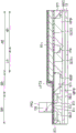
Fig. 5 is a flowchart showing a flow of manufacturing steps for hybrid loading of a field effect transistor as a constituent of a main circuit and a MONOS transistor as a constituent of an additional circuit in the related art. In the flow chart shown in fig. 5, the steps requiring an additional mask for the mixed loading of the MONOS transistor are surrounded by a dotted line.
As shown in fig. 5, first, a well is formed in the main circuit formation region (S1001). Then, a well is formed in the memory formation region (S1002). At this time, an additional mask MSK1 covering the main circuit formation region and exposing the memory formation region is used. This means that an additional mask MSK1 is required to form the well of the MONOS transistor in the memory formation region.
Next, a gate electrode is formed in the memory formation region (S1003). At this time, an additional mask MSK2 is required to form the gate electrode of the MONOS transistor in the memory formation region. Then, a gate electrode of the field effect transistor is formed in the main circuit forming region (S1004).
Next, n is formed in the memory formation region-A type semiconductor region (extension region) (S1005). At this time, n of the MONOS transistor is formed in the memory formation region-The type semiconductor region requires an additional mask MSK 3. Then, n of the field effect transistor is formed in the main circuit forming region-The type semiconductor region (S1006).
Then, a sidewall spacer is formed on each of a sidewall of the gate electrode of the MONOS transistor and a sidewall of the gate electrode of the field effect transistor (S1007). Then, n is formed in the memory formation region+The type semiconductor region (diffusion layer) (S1008). At this time, n of the MONOS transistor is formed in the memory formation region+The type semiconductor region requires an additional mask MSK 4. Then, n of the field effect transistor is formed in the main circuit forming region+A type semiconductor region (S1009).
No additional mask is required for the steps after this, and thus their explanation is omitted. In the related art, therefore, a field effect transistor as a constituent of the main circuit and a MONOS transistor as a constituent of the additional circuit can be mixed and mounted. As shown in fig. 5, the manufacturing steps of the semiconductor device in the related art require four additional masks MSK1 to MSK4 for the mixed loading of MONOS transistors (additional circuits) and base products (main circuits). In this regard, it is desirable to reduce the number of masks required for hybrid loading of MONOS transistors and thereby reduce the manufacturing cost of semiconductor devices. It is desirable to further reduce the number of additional masks (four masks) used in the prior art. Therefore, in the first embodiment, a measure is taken to make the number of masks added for the mixed loading of the MONOS transistor smaller than that in the related art. Next, the technical idea of the first embodiment for taking this measure will be explained.
< basic idea of first embodiment >
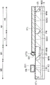
Fig. 6 is a flowchart showing a flow of manufacturing steps for hybrid loading of a field effect transistor as a constituent of a main circuit and a MONOS transistor as a constituent of an additional circuit. In the flowchart shown in fig. 6, the step requiring an additional mask for the mixed loading of the MONOS transistor is surrounded by a dotted line.
As shown in fig. 6, a well is formed in the main circuit forming region (S101). Then, a well is formed in the memory formation region (S102). At this time, an additional mask MSK1 covering the main circuit formation region and simultaneously exposing the memory formation region is used. This means that an additional mask MSK1 is required to form the well of the MONOS transistor in the memory formation region.
Next, a gate electrode is formed in the memory formation region (S103). At this time, an additional mask MSK2 is required to form the gate electrode of the MONOS transistor in the memory formation region. Then, in the first embodiment, n is formed in the memory formation region by using an additional mask for forming the gate electrode of the MONOS transistor in the memory formation region without changing it to another one-A type semiconductor region (extension region) (S1004). This means that in the first embodiment, n is formed by ion implantation in alignment with the gate electrode of the MONOS transistor using an additional mask for patterning of the formation of the gate electrode of the MONOS transistor without changing it to another one-A type semiconductor region. In other words, in the first embodiment, the process for forming the gate electrode of the MONOS transistor is performed in alignment with the process for forming n with the gate electrode of the MONOS transistor-The mask is shared between the ion implantations of the type semiconductor regions. The first embodiment thus enables a reduction in the number of masks added for mixed loading of MONOS transistors (first mask reduction effect).
Next, a gate electrode of the field effect transistor is formed in the main circuit forming region (S105). Then, n of the field effect transistor is formed in the main circuit forming region-And a type semiconductor region (S106). Next, a sidewall spacer is formed on each of a sidewall of the gate electrode of the MONOS transistor and a sidewall of the gate electrode of the field effect transistor (S107). Then, n of the MONOS transistor is formed in the memory formation region+N-type semiconductor region (diffusion layer) and simultaneously forming field effect transistor in main circuit forming region+The type semiconductor region (diffusion layer) (S108). This means that in the first embodiment, n of the MONOS transistor is formed at the same time+N-type semiconductor region and field effect transistor+A type semiconductor region. In other words, in the first embodiment, n of the MONOS transistor is simultaneously formed by ion implantation using a common mask+N-type semiconductor region and field effect transistor+A type semiconductor region.
In the first embodiment, therefore, n of the MONOS transistor+No additional mask is required for the formation of the type semiconductor region. Therefore, in the first embodiment, the MONOS transistor can be mixedly loaded while reducing the number of additional masks (second mask reduction effect).
Therefore, in the first embodiment, the number of masks to be added for the mixed loading of the MONOS transistor can be made smaller than that of the related art due to the first mask reduction effect and the second mask reduction effect. Specifically, in the related art, the mixed loading of the MONOS transistor (additional circuit) and the base product (main circuit) requires four additional masks MSK1 to MSK 4. On the other hand, in the first embodiment, the mixed loading of the MONOS transistor (additional circuit) and the base product (main circuit) can be realized using the two additional masks MSK1 and MSK 2. In the semiconductor device of the first embodiment, the MONOS transistor can be mixedly loaded as an additional circuit to be added to the main circuit while minimizing variations in the manufacturing process of the base product having the main circuit therein. Therefore, the manufacturing cost of the semiconductor device can be reduced.
< method of manufacturing semiconductor device in first embodiment > (MONOS LAST)
A method of manufacturing the semiconductor device in the first embodiment will be specifically described below with reference to some drawings. The method of manufacturing the semiconductor device in the first embodiment is referred to as "MONOS LAST". This "MONOS LAST" is a method of first forming a conductor film (first conductor film) to be processed into a gate electrode of a field effect transistor that will be a constituent component of a main circuit and then forming a conductor film (second conductor film) to be processed into a gate electrode of a MONOS transistor that will be a constituent component of an additional circuit. The manufacturing method called "MONOS LAST" is advantageous in that the influence of a thermal load applied when forming the field effect transistor of the main circuit on the MONOS transistor of the additional circuit can be suppressed. Therefore, a manufacturing method called "MONOS LAST" is a useful manufacturing method from the viewpoint of suppressing the application of an excessive thermal load to the MONOS transistor and thereby reducing the variation in the characteristics of the MONOS transistor to be a constituent component of an additional circuit.
First, as shown in fig. 7, a semiconductor substrate 1S made of a silicon single crystal implanted with a p-type impurity such as boron (B) is provided. The semiconductor substrate 1S is a semiconductor wafer having a substantially disk shape at this time. An element isolation region STI is formed in the semiconductor substrate 1S. The element isolation region STI is provided in order to prevent interference between elements. This element isolation region STI can be formed, for example, by STI (shallow trench isolation). In the STI method, an element isolation region STI is formed in the following manner. Specifically, an element isolation trench is formed in the semiconductor substrate 1S by photolithography and etching. An insulating film (silicon oxide film or the like) is formed on the semiconductor substrate 1S so as to fill the element isolation trench. Then, an unnecessary portion of the silicon oxide film on the semiconductor substrate 1S is removed by Chemical Mechanical Polishing (CMP). The element isolation region STI is thus formed by filling only the element isolation trench with an insulating film (silicon oxide film or the like). As shown in fig. 7, by the element isolation region STI, the memory formation region MR and the main circuit formation region AR are separated from each other via the barrier region BR and the main circuit formation region AR is separated into the low breakdown voltage MISFET formation region LR and the high breakdown voltage MISFET formation region HR.
Then, a well isolation layer NISO made of an n-type semiconductor region is formed in the semiconductor substrate 1S by implanting n-type impurities such As phosphorus (P) or arsenic (As) into the semiconductor substrate 1S. Then, by photolithography and ion implantation, a p well PW is formed in the semiconductor substrate 1S of the low breakdown voltage MISFET forming region LR and a p well HPW is formed in the semiconductor substrate 1S of the high breakdown voltage MISFET forming region HR. An isolation layer HNW is formed below the element isolation region STI formed in the boundary region BR. Then, in the low breakdown voltage MISFET forming region LR, a conductive impurity is implanted into the channel region of the p well PW by ion implantation so as to adjust the threshold voltage of the low breakdown voltage MISFET. Meanwhile, in the high breakdown voltage MISFET forming region HR, a conductive type impurity is implanted into the channel region of the p-well HPW by ion implantation in order to adjust the threshold voltage of the high breakdown voltage MISFET
Next, after the surface of the semiconductor substrate 1S is washed with hydrofluoric acid or the like, a gate insulating film GOX1 is formed on the semiconductor substrate 1S of the low breakdown voltage MISFET forming region LR and a gate insulating film GOX2 is formed on the semiconductor substrate 1S of the high breakdown voltage MISFET forming region HR and the memory forming region MR. The gate insulating film GOX1 and the gate insulating film GOX2 are each made of, for example, a silicon oxide film and the thickness of the gate insulating film GOX1 is smaller than that of the gate insulating film GOX 2.
Next, a polysilicon film (polycrystalline silicon film) PF1 is formed on the entire main surface of the semiconductor substrate 1S. As shown in fig. 8, after a resist film PR1 is formed on the polysilicon film PF1 by coating, the resist film PR1 is patterned by photolithography. Patterning of the resist film PR1 is performed so as to cover the main circuit formation region AR and expose the memory formation region MR. The patterned resist film PR1 is used as an additional mask MSK1 shown in the flowchart of fig. 6. The polysilicon film PF1 and the gate insulating film GOX2 formed in the memory formation region MR are removed by etching using the patterned resist film PR1 as a mask. Then, a p-well MPW is formed in the semiconductor substrate 1S of the memory formation region MR by ion implantation using the patterned resist film PR1 as a mask. Further, in the memory formation region MR, a conductive type impurity is implanted into the channel region in the p-well MPW by ion implantation in order to adjust the threshold voltage of the MONOS transistor.
Next, as shown in fig. 9, an insulating film IF1 is formed on the semiconductor substrate 1S and the polysilicon film PF1, and then a charge storage film EC is formed on the insulating film IF 1. Then, an insulating film IF2 is formed on the charge storage film EC, and then, a polysilicon film PF2 is formed on the insulating film IF 2. The insulating film IF1 is made of, for example, a silicon oxide film and for its formation, ISSG oxidation capable of forming a dense silicon oxide film with good film quality can be used. The insulating film IF1 has a thickness of about 4 nm. The charge storage film EC is made of a silicon nitride film and may be formed by CVD, for example. The charge storage film EC has a thickness of about 10 nm. The insulating film IF2 is made of a silicon oxide film and for its formation, HTO (high temperature oxide) capable of forming a dense silicon oxide film with good film quality can be used. The insulating film IF2 has a thickness of about 5 nm. The polysilicon film PF2 may be formed using, for example, CVD. In this way, a stacked insulating film (ONO film) which is dense, has excellent tolerance for an insulation resistance value, and has good film quality can be formed.
Next, as shown in fig. 10, after a resist film PR2 is formed on the polysilicon film PF2 by coating, the resist film PR2 is patterned by photolithography. Patterning of the resist film PR2 is performed so as to cover the gate electrode formation region of the memory formation region MR and expose the main circuit formation region AR. The patterned resist film PR2 thus obtained becomes the additional mask MSK2 shown in the flowchart of fig. 6. Then, the polysilicon film PR2 is patterned by etching using the patterned resist film PR2 as a mask to form a gate electrode CG in the memory formation region MR. At this time, as shown in fig. 10, in the boundary region BR, the remnants LFT3 of the polysilicon film PF2 are formed in the form of sidewalls. Then, as shown in fig. 11, the exposed insulating film IF2, charge storage film EC, and insulating film IF1 are removed using, for example, dry etching. Accordingly, the stacked insulating film composed of the insulating film IF1, the charge storage film EC, and the insulating film IF2 remains below the gate electrode CG formed in the memory formation region MR, while the residue portion LFT2 composed of the insulating film IF2, the charge storage film EC, and the insulating film IF1 is formed in a portion of the boundary region BR covered with the residue portion LFT 3.
Then, n is formed in the semiconductor substrate 1S of the memory formation region MR by ion implantation in alignment with the gate electrode CG using a mask made of the patterned resist film PR2 without modifying it to another one-A type semiconductor region (extension region or lightly doped impurity diffusion region) MLD. This means that in the first embodiment, the process at the time of formation of the gate electrode for the MONOS transistor is aligned with n for the gate electrode CG of the MONOS transistor-The mask is shared between the ion implantations for the formation of the type semiconductor region MLD. Therefore, according to the first embodiment, the number of additional masks required for the mixed loading of the MONOS transistor can be reduced.
In the ion implantation step shown in fig. 12, since the polysilicon film PF1 formed in the main circuit forming region AR is exposed, an n-type impurity is also implanted in this polysilicon film PF 1. However, also in this case, by controlling the implantation energy in the ion implantation step, it is possible to prevent the n-type impurity from penetrating the polysilicon film PF1 and being implanted into the semiconductor substrate 1S of the main circuit formation region AR.
Since the n-type impurity has been implanted into the polysilicon film PF1 at a concentration several orders of magnitude higher than that in the ion implantation step shown in fig. 12 in order to protect the conductivity of the polysilicon film PF1, the implantation of the n-type impurity into the polysilicon film PF1 through the ion implantation step shown in fig. 12 does not cause any problem. In the main circuit formation region AR, not only the n-channel type field effect transistor but also the p-channel type field effect transistor is formed and a p-type impurity is implanted into the polysilicon film PF1 in the p-channel type field effect transistor formation region. However, the concentration of the p-type impurity is also high, so that the n-type impurity implantation in the ion implantation step shown in fig. 12 does not cause any problem.
Next, as shown in fig. 13, after removing the patterned resist film PR2, a resist film PR3 extending from the memory formation region MR to the main circuit formation region AR is formed by coating. More specifically, a resist film PR3 is formed by coating so as to cover the gate electrode CG formed in the memory formation region MR and extend over the polysilicon film PF1 formed in the main circuit formation region AR. Then, the resist film PR3 is patterned by photolithography. Patterning of the resist film PR3 is performed so as to cover the memory formation region MR and, at the same time, the gate electrode formation region of the main circuit formation region AR. By etching using the patterned resist film PR3 as a mask, the polysilicon film PF1 is processed and the gate electrode G1 and the gate electrode G2 are formed in the low breakdown voltage MISFET forming region LR of the main circuit forming region AR and in the high breakdown voltage MISFET forming region HR of the main circuit forming region AR, respectively. Meanwhile, a residue portion LFT1, which is a residue of the polysilicon film PF1, is formed in the boundary region BR. Therefore, in the boundary region BR, the residue pattern LFT having a structure in which the residue portion LFT1 has the residue portion LFT3 on the side wall thereof via the residue portion LFT2 remains.
Next, as shown in fig. 14, after removing the patterned resist film PR3, a resist film PR4 is formed on the semiconductor substrate 1S by coating. The resist film PR4 is then patterned by photolithography. Patterning of the resist film PR4 is performed so as to cover the memory formation region MR, the boundary region BR, and the low breakdown voltage MISFET formation region LR while exposing the high breakdown voltage MISFET formation region HR. Then, n is formed in the semiconductor substrate 1S of the high breakdown voltage MISFET formation region HR in alignment with the gate electrode G2 by ion implantation using the patterned resist film PR4 as a mask-A type semiconductor region HNLD.
Next, as shown in fig. 15, after removing the patterned resist film PR4, a resist film PR5 is formed on the semiconductor substrate 1S by coating. Then, the resist film PR5 is patterned by photolithography. Patterning of the resist film PR5 is performed so as to cover the memory formation region MR, the boundary region BR, the high breakdown voltage MISFET formation region HR, while exposing the low breakdown voltage MISFET formation region LR. Then, n is formed in the semiconductor substrate 1S of the low-breakdown-voltage MISFET formation region LR in alignment with the gate electrode G1 by ion implantation using the patterned resist film PR5 as a mask-The type semiconductor region LNLD.
Next, after removing the patterned resist film PR5, a stacked film of a silicon oxide film, a silicon nitride film, and a silicon oxide film is formed on the semiconductor substrate 1S as shown in fig. 16. For the formation of the silicon oxide film and the silicon nitride film, CVD, for example, can be used. Then, the stacked film is subjected to anisotropic etching to form the side wall SW. More specifically, in the memory formation region MR, a sidewall SW (stacked structure: gate electrode CG + ONO film) is formed on both sidewalls of the gate electrode CG. On the other hand, in the low breakdown voltage MISFET forming region LR of the main circuit forming region AR, the side walls SW are formed on both side walls of the gate electrode G1, and in the high breakdown voltage MISFET forming region HR of the main circuit forming region AR, the side walls SW are formed on both side walls of the gate electrode G2. Also in the boundary region BR, a sidewall SW is formed on a sidewall of the residue pattern LFT.
Next, as shown in fig. 17, n is formed in the memory formation region MR in alignment with the side wall SW by using photolithography and ion implantation+A type semiconductor region (diffusion layer or heavily doped impurity diffusion region) NDF. n is+The type semiconductor region NDF is a semiconductor region implanted with n-type impurities such as phosphorus or arsenic. n is+Type semiconductor regions NDF and n-The type semiconductor region MLD is configured as a source region or a drain region of the MONOS transistor. By passing through n+Type semiconductor regions NDF and n-The type semiconductor region MLD forms each of a source region and a drain region of the MONOS transistor, which may each have an LDD (lightly doped drain) structure.
Through similar ion implantation steps, n is also formed in alignment with the side wall SW in the low breakdown voltage MISFET forming region LR of the main circuit forming region AR+A type semiconductor region NDF. n is+Type semiconductor regions NDF and n-The type semiconductor region LNLD is configured as a source region or a drain region of the low breakdown voltage MISFET. Also in low breakdown voltage MISFET, by respectively passing n+Type semiconductor regions NDF and n-The type semiconductor region LNLD forms each of the source region and the drain region, and the source region and the drain region of the low breakdown voltage MISFET may each have an LDD structure.
By the similar ion implantation step, n is also formed in alignment with the side wall SW in the high breakdown voltage MISFET forming region HR of the main circuit forming region AR+A type semiconductor region NDF. n is+Type semiconductor regions NDF and n-The type semiconductor region HNLD is configured as a source region or a drain region of the high breakdown voltage MISFET. Also in high breakdown voltage MISFET+Type semiconductor regions NDF and n-The type semiconductor region HNLD forms each of the source region and the drain region, and the source region and the drain region of the high breakdown voltage MISFET may each have an LDD structure.
Thus, in the first embodiment, n of the MONOS transistor+Type semiconductor region NDF, n of low breakdown voltage MISFET+Type semiconductor region NDF and n of high breakdown voltage MISFET+The type semiconductor regions NDF are formed together. This means that in the first embodiment, n of the MONOS transistor is formed simultaneously by ion implantation using a common mask+Type semiconductor region NDF, n of low breakdown voltage MISFET+Type semiconductor region NDF and n of high breakdown voltage MISFET+A type semiconductor region NDF. Thus, according to the first embodiment, n for a MONOS transistor+An additional mask for the formation of the type semiconductor region NDF becomes unnecessary. Therefore, according to the first embodiment, the number of additional masks required for the mixed loading of the MONOS transistor can be reduced.
Next, as shown in fig. 18, after a nickel platinum film (NiPt film) is formed on the semiconductor substrate 1S, heat treatment is performed to cause a reaction between the polysilicon film PF2 configuring the gate electrode CG and the nickel platinum film in the memory formation region MR to form a silicide film CS made of a nickel platinum silicide film (NiPtSi film). Therefore, the gate electrode CG has a stacked structure of the polysilicon film PF2 and the silicide film CS. Similarly, the silicon and nickel platinum films are on n+The surfaces of the type semiconductor regions NDF react with each other to form a silicide film CS.
Also in the low breakdown voltage MISFET forming region LR of the main circuit forming region AR, a silicide film CS made of a nickel platinum silicide film is formed on the surface of the polysilicon film PF1 configuring the gate electrode G1. Therefore, the gate electrode G1 is composed of the polysilicon film PF1 and the silicide film CS. As n+As a result of the reaction between silicon and the nickel platinum film on the surface of the type semiconductor region NDF, a silicide film CS made of a nickel platinum silicide film is also formed.
Also, the main circuit forming region AR is highIn breakdown voltage MISFET forming region HR, silicide film CS made of a nickel-platinum silicide film is formed on the surface of polysilicon film PF1 configuring gate electrode G2. Therefore, the gate electrode G2 is composed of the polysilicon film PF1 and the silicide film CS. Likewise, as n+As a result of the reaction between silicon and the nickel platinum film on the surface of the type semiconductor region NDF, a silicide film CS made of a nickel platinum silicide film is formed
In the first embodiment, the nickel platinum silicide film is formed, but, for example, a cobalt silicide film, a nickel silicide film, a titanium silicide film, or a platinum silicide film may be formed instead of the nickel platinum silicide film.
As described above, the MONOS transistor is formed in the memory formation region MR of the semiconductor substrate 1S, the low breakdown voltage MISFETQ1 is formed in the low breakdown voltage MISFET formation region LR of the main circuit formation region AR, and the high breakdown voltage MISFETQ2 is formed in the high breakdown voltage MISFET formation region HR of the main circuit formation region AR.
Next, a wiring step will be explained. As shown in fig. 19, a silicon nitride film SNF is formed on the main surface of the semiconductor substrate 1S. Then, as shown in fig. 20, by forming a silicon oxide film OXF on the silicon nitride film SNF, a contact interlayer insulating film IL composed of the silicon nitride film SNF and a silicon oxide film OXF can be formed. The surface contacting the interlayer insulating film IL is then planarized by using, for example, CMP (chemical mechanical polishing).
Next, as shown in fig. 20, the contact hole CNT is formed in the contact interlayer insulating film IL by using photolithography and etching. Then, as shown in fig. 3, a titanium/titanium nitride film is formed on the contact interlayer insulating film IL including the bottom surface and the inner wall of the contact hole CNT. The titanium/titanium nitride film is composed of a stacked film of a titanium film and a titanium nitride film and can be formed using, for example, sputtering. This titanium/titanium nitride film prevents tungsten, which is a material of the film to be filled in a later step, from diffusing into silicon. In short, it has a so-called barrier property.
A tungsten film is formed on the entire main surface of the semiconductor substrate 1S so as to fill the contact hole CNT. The tungsten film may be formed by CVD, for example. Unnecessary portions of the titanium/titanium nitride film and the tungsten film formed on the contact interlayer insulating film IL are removed by CMP, for example. Then, annealing is performed in a hydrogen atmosphere to form plug PLG.
Next, as shown in fig. 3, an interlayer insulating film IL1 made of, for example, a silicon oxide film is formed on the contact interlayer insulating film IL having the plug PLG therein. Then, a wiring trench is formed in the interlayer insulating film IL1 by photolithography and etching. Then, a tantalum/tantalum nitride film is formed on the interlayer insulating film IL1 and also in the wiring trench. The tantalum/tantalum nitride film may be formed, for example, by sputtering. Then, after a seed film made of a thin copper film is formed on the tantalum/tantalum nitride film by, for example, sputtering, a copper film is formed on the interlayer insulating film IL1 having the wiring trench therein by electroplating using the seed film as an electrode. Then, the exposed copper film on the interlayer insulating film IL1 except on the inner side of the wiring trench is polished and removed by, for example, CMP to leave only the copper film in the wiring trench formed in the interlayer insulating film IL 1. Therefore, the wiring W1 can be formed. Another wiring is formed over the wiring w1, but a description thereof is omitted. In this way, the semiconductor device of the first embodiment can be finally formed.
In the first embodiment, an example of forming the wiring W1 made of a copper film has been described. The wiring W1 may be formed of, for example, an aluminum film instead. In this case, a titanium/titanium nitride film, an aluminum film, and a titanium/titanium nitride film are formed in this order on the interlayer insulating film IL1 and the plug PLG. These films may be formed using, for example, sputtering. Then, these films were patterned into a wiring W1 by using photolithography and sputtering. Therefore, the wiring W1 made of an aluminum film can be formed.
< characteristics in the first embodiment >
Next, the characteristics of the first embodiment will be explained. A first characteristic in the first embodiment is that, as shown in fig. 10 to 12, the polysilicon film PF2 is processed with the patterned resist film PR2 as a mask to form the gate electrode CG in the memory formation region MR; and then, n is formed in the semiconductor substrate 1S of the memory formation region MR by ion implantation in alignment with the gate electrode CG using the mask without changing it to another one-The type semiconductor region MLD. In other words, the first embodimentIs formed on the gate electrode CG of the MONOS transistor MC by a process, and n for self-alignment with the gate electrode CG of the MONOS transistor MC-The mask is shared between the ion implantations for the formation of the type semiconductor region MLD. Therefore, in the first embodiment, the number of additional masks required for the mixed loading of the MONOS transistor MC can be reduced.
Next, a second characteristic of the first embodiment is that, as shown in fig. 17, n of the MONOS transistor MC is formed at the same time+Type semiconductor region NDF, n of low breakdown voltage MISFETQ1+Type semiconductor region NDF and n of high breakdown voltage MISFETQ2+A type semiconductor region NDF. In other words, the second characteristic of the first embodiment is that n of the MONOS transistor MC is simultaneously formed by ion implantation using a common mask+Type semiconductor region NDF, n of low breakdown voltage MISFETQ1+Type semiconductor region NDF and n of high breakdown voltage MISFETQ2+A type semiconductor region NDF. According to the second characteristic of the first embodiment, n for forming the MONOS transistor MC+An additional mask of the type semiconductor region NDF becomes unnecessary. The first embodiment thus makes it possible to reduce the number of additional masks required for the mixed loading of the MONOS transistor MC.
In the first embodiment having both the first characteristic and the second characteristic, the number of masks to be added for the mixed loading of the MONOS transistor MC can be made smaller than that in the related art. More specifically, in the prior art, the mixed loading of MONOS transistor MC (additional circuit) and base product (main circuit) requires four extra masks. On the other hand, in the first embodiment, the MONOS transistor MC (additional circuit) can be mixed-loaded with the base product (main circuit) by using only two extra masks. According to the semiconductor device of the first embodiment, while minimizing variations in the manufacturing process of the base product having the main circuit therein, the MONOS transistor can be mixedly loaded as an additional circuit to be added to the main circuit.
In association with the second characteristic of the first embodiment, it seems that n of the MONOS transistor MC can be formed at the same time-A type semiconductor region MLD,N of low breakdown voltage MISFETQ1-Type semiconductor region LNLD and n of high breakdown voltage MISFETQ2-A type semiconductor region HNLD. However, from the viewpoint of write operation or disturb characteristics, it is difficult to construct n of low breakdown voltage MISFETQ1 of the main circuit-Type semiconductor region LNLD and n of high breakdown voltage MISFETQ2-Type semiconductor region HNLD simultaneously forms n of MONOS transistor as the same semiconductor region-The type semiconductor region MLD. Therefore, in the first embodiment, n of the MONOS transistor MC is formed-Step of forming semiconductor region MLD and forming n of low breakdown voltage MISFETQ1-Step of forming type semiconductor region LNLD or n for forming high breakdown voltage MISFETQ2-The steps of the type semiconductor region HNLD are performed separately, but the number of additional masks is reduced based on the first characteristic. On the other hand, n of the MONOS transistor MC can be formed simultaneously as the same semiconductor region by appropriate optimization+Type semiconductor region NDF, n of low breakdown voltage MISFETQ1+Type semiconductor region NDF and n of high breakdown voltage MISFETQ2+The type semiconductor region NDF, and therefore, the number of additional masks is reduced based on the second characteristic.
In the first embodiment, the number of additional masks can be reduced by taking the measures described as the first and second characteristics in the ion implantation step for forming the source region and the drain region of the MONOS transistor MC. Therefore, in the first embodiment, since the number of additional masks is reduced, the manufacturing cost of the semiconductor device can be reduced.
Next, a third characteristic of the first embodiment will be explained. Fig. 21 is an explanatory diagram of a third characteristic in the first embodiment. In the method of manufacturing the semiconductor device of the first embodiment, the polysilicon film PF2 for the formation of the gate electrode CG of the MONOS transistor MC is different from the polysilicon film PF1 for the formation of the gate electrode G1 of the low breakdown voltage MISFETQ1 or the gate electrode G2 of the high breakdown voltage MISFETQ2, so that a residual pattern is inevitably formed in the boundary region BR.
Here, for example, fig. 21B illustrates a technique of leaving a resist film in the boundary region BR and thereby intentionally forming a large-size residue pattern lft (p). As shown in fig. 21B, the large-sized residue pattern lft (p) thus formed increases the adhesive force of the residue pattern lft (p), so that it provides an advantage of preventing the residue pattern from peeling and becoming foreign matter. However, increasing the size of the residue pattern has the following disadvantages in view of hybrid loading of the MONOS transistor as an additional circuit to be added to the main circuit while minimizing variations in the manufacturing process of the main circuit. Specifically, as shown in fig. 21B, increasing the size of the residue pattern lft (p) decreases the distance LB between the surface contacting the interlayer insulating film and the upper surface of the residue pattern lft (p). This means that the thickness L2 of the contact interlayer insulating film needs to be increased. In other words, increasing the size of the residue pattern lft (p) is useful from the viewpoint of preventing peeling of the residue pattern lft (p), but this technique requires variation in the manufacturing process of the main circuit in order to secure the distance LB between the surface of the contact interlayer insulating film and the upper surface of the residue pattern lft (p). This process therefore makes it difficult to minimize variations in the manufacturing process of the main circuit when the MONOS transistor is hybrid loaded. Therefore, it increases the manufacturing cost due to variations in the manufacturing process of the main circuit.
On the other hand, fig. 21A shows the shape of the residue pattern LFT formed in the boundary region BR in the first embodiment. In the first embodiment, as shown in fig. 21A, the residue pattern LFT is formed without leaving the resist film in the boundary region BR (third characteristic). In this case, the height of the residue pattern LFT is not more than the height of the gate electrode of the field effect transistor formed in the main circuit forming region AR. This means that in the first embodiment, the distance LA between the surface of the contact interlayer insulating film and the upper surface of the residue pattern LFT can be secured. Therefore, according to the first embodiment, it is not necessary to change the thickness L1 of the contact interlayer insulating film and variations in the manufacturing process of the main circuit can be minimized. Therefore, according to the first embodiment, an increase in manufacturing cost due to a variation in the manufacturing process of the main circuit can be avoided.
The first embodiment has a significant effect on reduction of manufacturing cost of a semiconductor device having the MONOS transistor MC as an additional circuit to be added to the main circuit due to a synergistic effect of the first and second characteristics enabling reduction of the number of additional masks and the third characteristic enabling minimization of variation in the manufacturing process of the main circuit.
< modified example 1>
Next, modified example 1 will be explained. The manufacturing method of the semiconductor device in modification example 1 is substantially similar to that of the semiconductor device of the first embodiment, and therefore the differences therebetween will be mainly explained.
The steps shown in fig. 7 to 9 are performed similarly to the first embodiment. Then, as shown in fig. 22, a resist film PR2 is formed on the polysilicon film PF2 by coating and the thus formed resist film PR2 is patterned using photolithography. Patterning of the resist film PR2 is performed so as to cover the gate electrode formation region of the memory formation region MR and expose the main circuit formation region AR. The polysilicon film PR2 is patterned by etching using the patterned resist film PR2 as a mask to form a gate electrode CG in the memory formation region MR.
Next, as shown in fig. 23, n is formed in the semiconductor substrate 1S of the memory formation region MR by ion implantation in alignment with the gate electrode CG using the patterned resist film PR2 as a mask without modifying it to another one-The type semiconductor region MLD. Also in modified example 1, the process at the formation of the gate electrode CG for the MONOS transistor is aligned with n for the gate electrode CG of the MONOS transistor-The mask is shared between the ion implantations for the formation of the type semiconductor region MLD. Also in modified example 1, this makes it possible to reduce the number of additional masks for mixed loading of MONOS transistors.
In modification example 1, as shown in fig. 23, n is formed in a semiconductor substrate 1S via a stacked insulating film composed of an insulating film IF1, a charge storage film EC, and an insulating film IF2 and exposed from a gate electrode CG-The type semiconductor region MLD. In short, the characteristics of modified example 1 were such that n was formed by ion implantation-The type semiconductor region MLD while leaving the stacked insulating film exposed from the gate electrode CG.
Then, as shown in fig. 24, the exposed insulating film IF2, charge storage film EC, and insulating film IF1 are then removed by, for example, dry etching. The steps after this are similar to those of the first embodiment.
As described above, in the manufacturing method of the semiconductor device in modification example 1, since n is formed via stacking the insulating films (the insulating film IF1, the charge storage film EC, and the insulating film IF2)-The type semiconductor region MLD (as shown in fig. 23) can protect the surface of the semiconductor substrate 1S from damage that can occur at the time of ion implantation. In other words, in modification example 1, due to the presence of the stacked insulating films, damage that can occur at the time of ion implantation can be reduced, and at the same time, the surface of the semiconductor substrate 1S can be prevented from suffering contamination that can be caused by ion implantation. Further, the stacked insulating film remaining on the polysilicon film PF1 in the main circuit formation region AR effectively prevents the ion-implanted conductive type impurities from easily penetrating the polysilicon film PF 1.
< modified example 2>
Next, modified example 2 will be explained. The manufacturing method of the semiconductor device in modification example 2 is almost similar to that of the semiconductor device of the first embodiment, and therefore the difference therebetween will be mainly explained.
In a manner similar to the first embodiment, the steps shown in fig. 7 to 9 are performed. Then, as shown in fig. 25, a resist film PR2 is formed by coating on the polysilicon film PF2 and the resist film PR2 is patterned using photolithography. Patterning of the resist film PR2 is performed so as to cover the gate electrode formation region of the memory formation region MR and simultaneously expose the main circuit formation region AR. The polysilicon film PR2 is patterned by etching using the patterned resist film PR2 as a mask to form a gate electrode CG in the memory formation region MR.
Next, as shown in fig. 26, after removing the mask made of the patterned resist film PR2, the insulating film IF2 exposed from the gate electrode CG is removed by, for example, wet etching. Then, the exposed surface of the gate electrode CG is oxidized to form a silicon oxide film OX1 on the exposed surface of the gate electrode CG.
Then, as shown in FIG. 27, for exampleThe charge storage film EC made of a silicon nitride film is removed with hot phosphoric acid as by wet etching. Then, as shown in fig. 28, n is formed in the semiconductor substrate 1S of the memory formation region MR in alignment with the gate electrode CG by ion implantation using the gate electrode CG as a mask-The type semiconductor region MLD. In fig. 28, n may also be formed in the semiconductor substrate 1S of the memory formation region MR by ion implantation using the gate electrode CG as a mask in alignment with the gate electrode CG after removing the insulating film IF1 exposed from the gate electrode CG by wet etching-The type semiconductor region MLD. The steps after this are similar to those of the first embodiment.
As described above, in the manufacturing method of the semiconductor device in modification example 2, the semiconductor substrate 1S can be prevented from suffering damage due to dry etching because the stacked insulating film is removed not by dry etching but by wet etching. Further, in modification example 2, a silicon oxide film OX1 is formed on the exposed surface of the gate electrode CG and this silicon oxide film OX1 is used as an offset spacer during the ion implantation step using the gate electrode CG as a mask, so that the short channel effect at the MONOS transistor MC can be suppressed.
< modified example 3>
Next, modified example 3 will be explained. The manufacturing method of the semiconductor device in modification example 3 is substantially similar to that of the semiconductor device of the first embodiment, and therefore the differences therebetween will be mainly explained.
In a manner similar to the first embodiment, the steps shown in fig. 7 to 9 are performed. Then, as shown in fig. 29, a resist film PR2 is formed by coating on the polysilicon film PF2 and the resist film PR2 is patterned using photolithography. Patterning of the resist film PR2 is performed so as to cover the gate electrode formation region of the memory formation region MR and simultaneously expose the main circuit formation region AR. The polysilicon film PR2 is patterned by etching using the patterned resist film PR2 as a mask to form a gate electrode CG in the memory formation region MR.
Next, as shown in fig. 30, the patterned resist film PR2 is used as a mask without modifying it to be a maskOn the other hand, n is formed in the semiconductor substrate 1S of the memory formation region MR by ion implantation in alignment with the gate electrode CG-The type semiconductor region MLD. At this time, in modification example 3, n is formed in the semiconductor substrate 1S via the stacked insulating films (the insulating film IF1, the charge storage film EC, and the insulating film IF2) exposed from the gate electrode CG-The type semiconductor region MLD.
Then, as shown in fig. 31, after the mask made of the patterned resist film PR2 is removed, the insulating film IF2 exposed from the gate electrode CG is removed by, for example, wet etching. Then, the exposed surface of the gate electrode CG is oxidized to form a silicon oxide film OX1 on the exposed surface of the gate electrode CG.
Next, as shown in fig. 32, the charge storage film EC made of a silicon nitride film is removed with hot phosphoric acid by, for example, wet etching. After the step shown in fig. 32, the insulating film IF1 (not shown) exposed from the gate electrode CG is removed by wet etching. The steps after this are similar to those of the first embodiment.
As described above, modifying the manufacturing method of the semiconductor device in example 3 can suppress the semiconductor substrate 1S from being damaged by dry etching because the stacked insulating film is removed not by dry etching but by wet etching.
(second embodiment)
In the second embodiment, a description will be given of a semiconductor device having both a main circuit having a power transistor and a MONOS transistor included in an additional circuit.
< example of layout configuration of semiconductor chip >
Fig. 33 shows an example of the layout configuration of the semiconductor chip CHP2 of the second embodiment. In fig. 33, the semiconductor chip CHP2 of the second embodiment has an analog circuit 4, a nonvolatile memory 5, an I/O circuit 6, a logic circuit 7, and a driver circuit 8. The logic circuit 7 is constituted by, for example, an n-channel type low breakdown voltage MISFET (n-type MISFET) and a p-channel type low breakdown voltage MISFET (p-type MISFET), and the driver circuit 8 is constituted by, for example, an n-channel type power transistor (n-type power transistor) and a p-channel type power transistor (p-type power transistor).
The main circuit is constituted by the analog circuit 4, the logic circuit 7, and the driver circuit 8, and the additional circuit is constituted by the nonvolatile memory 5. In short, the semiconductor chip CHP2 of the second embodiment has a main circuit that realizes a main function and an additional circuit to be added to the main circuit. In the second embodiment, a MONOS transistor is used for the additional circuit. In particular, in the second embodiment, the additional circuit is constituted by an electrical fuse to be used for voltage adjustment after completion of the wafer. By constructing this electric fuse from a MONOS transistor as a rewritable nonvolatile memory, an MTP (multiple programming) type electric fuse which can be adjusted repeatedly in a wafer form or a package form can be realized.
< device Structure of semiconductor chip >
Fig. 34 is a sectional view showing a device structure example of the semiconductor chip CHP2 in the second embodiment. Fig. 34 shows the memory formation region MR, the main circuit formation region AR, and the boundary region BR sandwiched between the memory formation region MR and the main circuit formation region AR. Main circuit formation region AR is composed of n-type MISFET formation region lr (n), p-type MISFET formation region lr (p), n-type power transistor formation region pwr (n), and p-type power transistor formation region pwr (p).
In fig. 34, a semiconductor substrate 1S has a buried insulating layer BOX thereon. The buried insulating layer BOX has a silicon layer SIL thereon. The silicon layer SIL has therein an element isolation region STI for isolating elements from each other. The active regions separated by the element isolation region STI become a memory formation region MR, an n-type MISFET formation region lr (n), a p-type MISFET formation region lr (p), an n-type power transistor formation region pwr (n), and a p-type power transistor formation region pwr (p), respectively. In particular, the element isolation region STI separating the n-type power transistor formation region pwr (n) from the p-type power transistor formation region pwr (p) has a deep trench isolation region DTI penetrating the silicon layer SIL and reaching the buried insulation layer BOX.
The MONOS transistor MC formed in the memory formation region MR has the following configuration. Specifically, an insulating film (barrier film) IF1 is provided on a p-well MPW formed in a silicon layer SIL and a charge storage film EC is provided on the insulating film IF 1. This charge storage film EC has thereon an insulating film (barrier film) IF2 and has thereon a gate electrode CG made of a conductive film on an insulating film IF 2. The gate electrode CG is composed of a stacked film of, for example, a polysilicon film PF2 and a silicide film CS in order to reduce the resistance. The gate electrode CG has, on both side walls thereof, side walls SW made of, for example, an insulating film to have an LDD structure.
With n in the silicon layer SIL under the sidewall SW-Type semiconductor regions MLD and n+The type semiconductor region NDF serves as a semiconductor region. The p-well MPW directly below the insulating film IF1 has a channel region therein.
Next, the configuration of the N-type MISFETQ1(N) formed in the N-type MISFET forming region lr (N) will be described. In the N-type MISFETQ1(N), a gate insulating film GOX1 is provided on a p-well PW formed in a silicon layer SIL and a gate electrode G1(N) is provided on this gate insulating film GOX 1. The gate insulating film GOX1 is made of, for example, a silicon oxide film, and the gate electrode G1(N) is made of, for example, a polysilicon film. The gate electrode G1(N) has sidewalls SW on both sidewalls thereof and N in the silicon layer SIL below this sidewall SW-Type semiconductor regions LNLD and n+The type semiconductor region NDF serves as a semiconductor region. The p-well PW directly under the gate insulating film GOX1 has a channel region therein.
Next, the configuration of the P-type MISFETQ1(P) formed in the P-type MISFET forming region lr (P) will be described. In the P-type MISFETQ1(P), a gate insulating film GOX1 is provided on an n-well NW formed in the silicon layer SIL and a gate electrode G1(P) is provided on this gate insulating film GOX 1. The gate insulating film GOX1 is made of, for example, a silicon oxide film, and the gate electrode G1(P) is made of, for example, a polysilicon film. The gate electrode G1(P) has sidewalls SW on both sidewalls thereof and P in the silicon layer SIL below this sidewall SW-Type semiconductor regions LPLD and p+The type semiconductor region PDF serves as a semiconductor region. The n-well NW directly under the gate insulating film GOX1 has a channel region therein.
Next, the configuration of the N-type power transistor Q3(N) formed in the N-type power transistor formation region pwr (N) will be explained. In the N-type power transistor Q3(N), the silicon layer SIL has an N-well NWL and a p-well PW separated from each other. The n-well NW is formed so as to be included in the n-well NWL. Form n+A type semiconductor region NDF (drain region) is so as to be contained in the n-well NW. On the other hand, form n+Type semiconductor regions NDF (Source region) and p+Type semiconductor region PDF(body contact region) so as to be contained in the p-type well PW (body region). Form n+Type semiconductor regions NDF and p+The type semiconductor regions PDF so as to be adjacent to each other. The silicon layer SIL has a gate insulating film GOX2 on its surface and the gate insulating film GOX2 has a gate electrode G3 (N). Gate electrode GOX2 is made of, for example, a silicon oxide film and gate electrode G3(N) is made of, for example, a polysilicon film.
Next, the configuration of the P-type power transistor Q3(P) formed in the P-type power transistor forming region pwr (P) will be explained. In the P-type power transistor Q3(P), the silicon layer SIL has a P-well HPW and an n-well NW separated from each other. The p-well PW is formed so as to be included in the p-well HPW. Form p+A type semiconductor region PDF (drain region) so as to be contained in the p-well PW. On the other hand, form p+Type semiconductor region PDF (Source region) and n+The type semiconductor region NDF (body contact region) is so as to be contained in the n-well NW (body region). Form p+Type semiconductor region PDF and n+The type semiconductor regions NDF are adjacent to each other. The silicon layer SIL has a gate insulating film GOX2 on its surface and the gate insulating film GOX2 has a gate electrode G3(P) thereon. Gate electrode GOX2 is made of, for example, a silicon oxide film and gate electrode G3(P) is made of, for example, a polysilicon film.
The border zone BR has a residue pattern LFT, which is a trace of a manufacturing step. More specifically, the residue pattern LFT in the second embodiment, as shown in fig. 34, is composed of: residue portion LFT3, which is a residue of a polysilicon film, residue portion LFT2, which is a residue of a stack insulating film composed of insulating film IF1, charge storage film EC, and insulating film IF2, and residue portion LFT1, which is a residue of a polysilicon film. Residue LFT3 is formed in the form of a side wall on the side surface of residue LFT1 via residue LFT 2.
< method of manufacturing semiconductor device in second embodiment > (MONOS LAST)
The semiconductor device of the second embodiment has the configuration as described above. The manufacturing method thereof will be described below with reference to some drawings. The method of manufacturing the semiconductor device of the second embodiment is referred to as "MONOS LAST". Such "MONOS LAST" is advantageous particularly in suppressing application of an excessive thermal load to the MONOS transistor. Specifically, the second embodiment is premised on a hybrid loading of a power transistor and a MONOS transistor. At this time, a considerable thermal load is applied to the power transistor as a manufacturing condition thereof because its use requires control of a large voltage or current. Therefore, when the power transistor and the MONOS transistor are mixedly loaded, a large thermal load during formation of the power transistor may have an influence on the characteristics of the MONOS transistor. In the second embodiment, the manufacturing method referred to as "MONOS LAST" can suppress application of an excessive thermal load to the MONOS transistor. A method of manufacturing a semiconductor device of the second embodiment using a manufacturing method called "MONOS LAST" will be described below.
First, in fig. 35, an SOI (silicon on insulator) having a buried insulating layer BOX on a semiconductor substrate 1S and a silicon layer SIL on the buried insulating layer BOX is provided. Then, an element isolation region STI is formed in the silicon layer SIL, thereby separating the memory formation region MR, the n-type MISFET formation region lr (n), the p-type MISFET formation region lr (p), the n-type power transistor formation region pwr (n), and the p-type power transistor formation region pwr (p) from each other. Then, by photolithography and ion implantation, a p well PW is formed in the silicon layer SIL of the n-type MISFET formation region lr (n) and an n well NW is formed in the silicon layer SIL of the p-type MISFET formation region lr (p). In the n-type power transistor formation region pwr (n), an n-well NWL, an n-well NW, and a p-well PW are formed. Also, in the silicon layer SIL of the p-type power transistor formation region pwr (p), a p-well HPW, a p-well PW, and an n-well NW are formed. Then, a gate insulating film GOX1 is formed on the surface of silicon layer SIL of each of n-type MISFET forming region lr (n) and p-type MISFET forming region lr (p), and a gate insulating film GOX2 is formed on the surface of silicon layer SIL of each of n-type power transistor forming region pwr (n) and p-type power transistor forming region pwr (p).
Next, as shown in fig. 36, a polysilicon film (polycrystalline silicon film) PF1 is formed on the entire surface of the SOI substrate. After a resist film PR6 was formed on the polysilicon film PF1 by coating, the resist film PR6 was patterned using photolithography. Patterning of the resist film PR6 is performed so as to cover the main circuit formation region AR and simultaneously expose the memory formation region MR. Then, the polysilicon film PF1 and the gate insulating film GOX1 are removed from the memory formation region MR by etching using the patterned resist film PR6 as a mask. Then, a p-well MPW is formed in the silicon layer SIL of the memory formation region MR by ion implantation using the patterned resist film PR6 as a mask. Further, in the memory formation region MR, a conductive type impurity is implanted into the channel region of the p-well MPW by ion implantation in order to adjust the threshold voltage of the MONOS transistor.
Next, as shown in fig. 37, an insulating film IF1 is formed on the SOI substrate and the polysilicon film PF1 and a charge storage film EC is formed on this insulating film IF 1. Then, an insulating film IF2 is formed on the charge storage film EC, and then a polysilicon film PF2 is formed on the insulating film IF 2. The insulating film IF1 is made of, for example, a silicon oxide film and for its formation, ISSG oxidation capable of forming a silicon oxide film which is dense and has good film quality can be used. The insulating film IF1 has a thickness of about 4 nm. The charge storage film EC is made of a silicon nitride film and may be formed by CVD, for example. The charge storage film EC has a thickness of about 10 nm. The insulating film IF2 is made of a silicon oxide film and for its formation, HTO (high temperature oxide) capable of forming a silicon oxide film which is dense and has good film quality can be used. The insulating film IF2 has a thickness of about 5 nm. The polysilicon film PF2 may be formed using, for example, CVD. In this way, a stacked insulating film (ONO film) which is dense, has excellent tolerance for the insulating resistance value, and has good quality can be formed.
Next, as shown in fig. 38, after a resist film PR7 is formed on the polysilicon film PF2 by coating, the resist film PR7 is patterned by photolithography. Patterning of the resist film PR7 is performed so as to cover the gate electrode formation region of the memory formation region MR and simultaneously expose the main circuit formation region AR. The polysilicon film PF2 is patterned by etching using the patterned resist film PR7 as a mask to form a gate electrode CG in the memory formation region MR. At this time, as shown in fig. 38, in the boundary region BR, the remnants LFT3 of the polysilicon film PF2 are formed in the form of sidewalls. Then, as shown in fig. 39, the exposed insulating film IF2, charge storage film EC, and insulating film IF1 are removed by, for example, dry etching. Therefore, the stacked insulating film composed of the insulating film IF1, the charge storage film EC, and the insulating film IF2 remains below the gate electrode CG formed in the memory formation region MR, and at the same time, the residue portion LFT2 composed of the insulating film IF2, the charge storage film EC, and the insulating film IF1 is formed in a portion of the boundary region BR covered with the residue portion LFT 3.
Then, as shown in fig. 40, n is formed in the silicon layer SIL of the memory formation region MR by ion implantation in alignment with the gate electrode CG using a mask made of the patterned resist mask PR7 without modifying it to another one-The type semiconductor region MLD. This means that in the second embodiment, the process at the formation of the gate electrode CG for the MONOS transistor is aligned with n for the gate electrode CG for the MONOS transistor-The mask is shared between the ion implantations for the formation of the type semiconductor region MLD. In the second embodiment, this makes it possible to reduce the number of additional masks required for the mixed loading of the MONOS transistor.
Next, as shown in fig. 41, after removing the patterned resist film PR7, a resist film PR8 extending from the memory formation region MR to the main circuit formation region AR is formed by coating. More specifically, a resist film PR8 is formed by coating so as to cover the gate electrode CG formed in the memory formation region MR and at the same time extend over the polysilicon film PF1 formed in the main circuit formation region AR. Then, the resist film PR8 is patterned by photolithography. Patterning of the resist film PR8 is performed so as to cover the memory formation region MR and, at the same time, the gate electrode formation region of the main circuit formation region AR. The polysilicon film PF1 was processed by etching using the patterned resist film PR8 as a mask. Therefore, the gate electrode G1(N) and the gate electrode G1(P) can be formed in the N-type MISFET forming region lr (N) and the P-type MISFET forming region lr (P) of the main circuit forming region AR, respectively. Likewise, gate electrode G3(N) and gate electrode G3(P) may be formed in N-type power transistor formation area pwr (N) and P-type power transistor formation area pwr (P) of main circuit formation area AR, respectively. At this time, in the boundary region BR, a residue portion LFT1 which is a residue of the polysilicon film PF1 is formed. Thus, the residue pattern LFT having a structure in which the residue portion LFT1 has the residue portion LFT3 on the side wall thereof via the residue portion LFT2 is retained in the boundary region BR.
Then, as shown in fig. 42, after removing the patterned resist film PR8, a resist film PR9 is formed on the SOI substrate by coating. The resist film PR9 is patterned by photolithography. Patterning of the resist film PR9 is performed so as to cover the memory formation region MR, the boundary region BR, the p-type MISFET formation region lr (p), the n-type power transistor formation region pwr (n), and the p-type power transistor formation region pwr (n) with them while exposing the n-type MISFET formation region lr (n). Then, N is formed in the silicon layer SIL of the N-type MISFET formation region lr (N) in alignment with the gate electrode G1(N) by ion implantation using the patterned resist film PR9 as a mask-The type semiconductor region LNLD.
Next, as shown in fig. 43, after removing the patterned resist film PR9, a resist film PR10 is formed on the SOI substrate by coating. The resist film PR10 is patterned by using photolithography. Patterning of the resist film PR10 is performed so as to cover the memory formation region MR, the boundary region BR, the n-type MISFET formation region lr (n), the n-type power transistor formation region pwr (n), and the p-type power transistor formation region pwr (n) with them while exposing the p-type MISFET formation region lr (p). Then, by ion implantation using the patterned resist film PR10 as a mask, P is formed in the silicon layer SIL of the P-type MISFET formation region lr (P) in alignment with the gate electrode G1(P)-The type semiconductor region LPLD.
Next, after removing the patterned resist film PR10, a silicon oxide film is formed on the SOI substrate, for example, as shown in fig. 44. The silicon oxide film can be formed by CVD, for example. Then, the silicon oxide film is anisotropically etched to form the side wall SW. More specifically, in the memory formation region MR, a sidewall SW (stacked structure: gate electrode CG + ONO film) is formed on both sidewalls of the gate electrode CG. On the other hand, in the N-type MISFET forming region lr (N) of the main circuit forming region AR, the sidewalls SW are formed on both sidewalls of the gate electrode G1(N), and in the P-type MISFET forming region lr (P) of the main circuit forming region AR, the sidewalls SW are formed on both sidewalls of the gate electrode G2 (P). Further, in N-type power transistor formation region pwr (N) of main circuit formation region AR, side walls SW are formed on both side walls of gate electrode G3(N), and in P-type power transistor formation region pwr (P) of main circuit formation region AR, side walls SW are formed on both side walls of gate electrode G3 (P). Also in the boundary region BR, a sidewall SW is formed on a sidewall of the residue pattern LFT.
Next, as shown in fig. 45, a resist film PR11 is formed on the SOI substrate by coating. The resist film PR11 is patterned by using photolithography. Patterning of the resist film PR11 is performed so as to expose regions other than the body contact regions of the memory formation region MR, the boundary region BR, the n-type MISFET formation region lr (n), and the n-type power transistor formation region pwr (n). Meanwhile, patterning of resist film PR11 is performed so as to cover the body contact regions of p-type MISFET forming region lr (p), n-type power transistor forming region pwr (n), and the regions of p-type power transistor forming region pwr (p) other than the body contact regions.
Then, n is formed in the memory formation region MR in alignment with the side wall SW by ion implantation using the patterned resist film PR11 as a mask+A type semiconductor region NDF. The source region or drain region of MONOS transistor is composed of n+Type semiconductor regions NDF and n-The type semiconductor region MLD is formed.
Through similar ion implantation steps, n is also formed in the n-type MISFET forming region lr (n) of the main circuit forming region AR in alignment with the side wall SW+A type semiconductor region NDF. The source region or drain region of n-type MISFET is composed of n+Type semiconductor regions NDF and n-The type semiconductor region LNLD is formed.
N is also formed in the n-type power transistor formation region pwr (n) of the main circuit formation region AR by a similar ion implantation step+A type semiconductor region NDF. Source or drain region of n-type power transistor+The type semiconductor region NDF is formed.
In addition, n is also formed in p-type power transistor formation region pwr (p) of main circuit formation region AR by a similar ion implantation step+Type semiconductor region NDF, the n+The type semiconductor region NDF will be a body contact region.
Thus, in the second embodiment, MONOS crystals are formed simultaneouslyN of a tube+NDF of type semiconductor region, n of n-type MISFET+Type semiconductor region NDF, n of n-type power transistor+Type semiconductor region NDF and n of p-type power transistor+A type semiconductor region NDF. This means that in the second embodiment, n of the MONOS transistor is formed simultaneously by ion implantation using a common mask+NDF of type semiconductor region, n of n-type MISFET+Type semiconductor region NDF, n of n-type power transistor+Type semiconductor region NDF and n of p-type power transistor+A type semiconductor region NDF. Thus, according to the second embodiment, n for forming a MONOS transistor+An additional mask of the type semiconductor region NDF becomes unnecessary. Therefore, the second embodiment makes it possible to reduce the number of additional masks required for the mixed loading of the MONOS transistor.
Next, as shown in fig. 46, after removing the patterned resist film PR11, a resist film PR12 is formed on the SOI substrate by coating. The resist film PR12 is patterned by using photolithography. Patterning of resist film PR12 is performed so as to cover memory formation region MR, boundary region BR, n-type MISFET formation region lr (n), a region of n-type power transistor formation region pwr (n) other than the body contact region, and the body contact region of p-type power transistor formation region pwr (p). Meanwhile, patterning of resist film PR12 is performed so as to expose the body contact regions of p-type MISFET forming region lr (p), n-type power transistor forming region pwr (n), and the regions of p-type power transistor forming region pwr (p) other than the body contact regions.
Then, by ion implantation using the patterned resist film PR12 as a mask, p is formed in the p-type MISFET forming region lr (p) of the main circuit forming region AR in alignment with the side wall SW+The type semiconductor region PDF. The source region or drain region of p-type MISFET is composed of p+Type semiconductor region PDF and n-The type semiconductor region LPLD is formed.
P is also formed in the n-type power transistor formation region pwr (n) of the main circuit formation region AR by a similar ion implantation step+Type semiconductor region PDF, p+The type semiconductor region PDF will be the body contact region.
In addition, through a similar ion implantation step, also in the main circuit forming regionP-type power transistor forming region PWR (P) of AR+The type semiconductor region PDF. Source or drain region of p-type power transistor+The type semiconductor region PDF is formed.
Next, as shown in fig. 47, in the element isolation region STI separating the n-type power transistor formation region pwr (n) from the p-type power transistor formation region pwr (p), a deep trench isolation region DTI penetrating the silicon layer SIL and reaching the buried insulation layer BOX is formed. The wiring step is then performed as in the first embodiment.
By the above method, the semiconductor device of the second embodiment in which the MONOS transistor MC, the N-type MISFETQ1(N), the P-type MISFETQ1(P), the N-type power transistor Q3(N), and the P-type power transistor Q3(P) are mixedly loaded can be manufactured.
(third embodiment)
In the third embodiment, a use example of a manufacturing method of a semiconductor device called "MONOS FIRST" will be explained next as a manufacturing method of a semiconductor device in which a main circuit including a field-effect transistor and a MONOS transistor included in an additional circuit are mixedly loaded.
< device Structure of semiconductor chip >
Fig. 48 is a sectional view showing a device structure example of the semiconductor chip CHP3 in the third embodiment. Fig. 48 shows the memory formation region MR, the main circuit formation region AR, and the boundary region BR sandwiched between the memory formation region MR and the main circuit formation region AR. The main circuit formation region AR is composed of the low breakdown voltage MISFET formation region LR and the high breakdown voltage MISFET formation region HR. The device structure of the semiconductor chip CHP3 in the third embodiment is substantially similar to that of the semiconductor chip CHP1 (see fig. 3) of the first embodiment, and therefore the differences therebetween will be mainly explained.
In the semiconductor chip CHP3 of the third embodiment, the residue pattern LFT formed in the boundary region BR is different from the residue pattern LFT of the first embodiment. This is due to the difference in the manufacturing method of the semiconductor device. A semiconductor device manufacturing method called "MONOS LAST" is used in the FIRST embodiment, and a semiconductor device manufacturing method called "MONOS FIRST" is used in the third embodiment. More specifically, a manufacturing method called "MONOS LAST" is used in the first embodiment, so that the residue pattern LET of the first embodiment has a structure in which the residue portion LFT1 has a residue portion LFT3 in the form of a sidewall via the residue portion LFT2 on the sidewall thereof as shown in fig. 3. On the other hand, in the third embodiment, a manufacturing method called "MONOS FIRST" is employed, and therefore, as shown in fig. 48, the residue pattern LFT of the third embodiment has a residue portion LFT1 in the form of a side wall in which the residue portion LFT3 has on a side wall thereof via the residue portion LFT 2. This means that in the first embodiment the residue LFT3 is in the form of a side wall, whereas in the third embodiment the residue LFT1 is in the form of a side wall.
Another device structure of the semiconductor chip CHP3 of the third embodiment is similar to that of the semiconductor chip CHP1 of the first embodiment.
< room for improvement >
The method of manufacturing the semiconductor device of the third embodiment is a method called "MONOS FIRST". "MONOS FIRST" is a manufacturing method of forming a conductor film to be processed into a gate electrode of a MONOS transistor as a constituent component of an additional circuit, that is, a second conductor film, and then forming a conductor film to be processed into a gate electrode of a field-effect transistor as a constituent component of a main circuit, that is, a FIRST conductor film. The manufacturing method referred to as "MONOS FIRST" is advantageous in that the influence of a thermal load applied during the formation of the MONOS transistor on the field effect transistor of the main circuit (base product) can be suppressed. The manufacturing method called "MONOS FIRST" is therefore effective particularly for suppressing application of an excessive thermal load to the field effect transistor configuring the main circuit and thereby reducing the variation in the characteristics of the field effect transistor as a constituent component of the main circuit.
In a manufacturing method of a semiconductor device called "MONOS FIRST" similar to a manufacturing method of a semiconductor device called "MONOS LAST", it is desirable to mixedly load a MONOS transistor as an additional circuit while minimizing variations in a manufacturing process of a base product having a main circuit therein. More specifically, the mixed loading of the MONOS transistor with the field effect transistor of the main circuit increases the number of masks, making it desirable to reduce the number of additional masks and thereby reduce the manufacturing cost of the semiconductor device. FIRST, a description will be given of a related art of "MONOS FIRST", and then, a description will be given of room for improvement of the related art.
Fig. 49 is a prior art flowchart showing a flow of manufacturing steps for mixing an effect transistor as a constituent of a main circuit and a MONOS transistor as a constituent of an additional circuit. In the flowchart shown in fig. 49, the step requiring an additional mask for the mixed loading of the MONOS transistor is surrounded by a dotted line.
First, as shown in fig. 49, a well is formed in the main circuit formation region (S2001). During the formation of the well, an additional mask MSK1 covering the main circuit formation region and exposing the memory formation region is used. This means that an additional mask MSK1 is required to form the well of the MONOS transistor in the memory formation region. A polysilicon film is formed on the entire main surface of a semiconductor substrate. The polysilicon film formed in the main circuit formation region is then removed while leaving the polysilicon film formed in the memory formation region (S2002). At this time, an additional mask MSK2 covering the memory formation region and simultaneously exposing the main circuit formation region is used. Then, a well is formed in the main circuit formation region (S2003).
Next, a gate electrode is formed in the main circuit forming region (S2004). Then, a gate electrode is formed in the memory formation region (S2005). At this time, an additional mask MSK3 is required to form the gate electrode of the MONOS transistor in the memory formation region.
Next, n is formed in the memory formation region-A type semiconductor region (extension region) (S2006). At this time, n of the MONOS transistor is formed in the memory formation region-The type semiconductor region requires an additional mask MSK 4. Next, n of the field effect transistor is formed in the main circuit forming region-A type semiconductor region (S2007).
Then, on each of a sidewall of a gate electrode of the MONOS transistor and a sidewall of a gate electrode of the field effect transistorSidewall spacers are formed (S2008). Then, n is formed in the memory formation region+A type semiconductor region (diffusion layer) (S2009). At this time, n of the MONOS transistor is formed in the memory formation region+The type semiconductor region requires an additional mask MSK 5. Next, n of the field effect transistor is formed in the main circuit forming region+The type semiconductor region (S2010).
This latter step does not require an additional mask, and thus their explanation is omitted. In the related art, a field effect transistor as a constituent of a main circuit and a MONOS transistor as a constituent of an additional circuit may be mixed and loaded in such a manner. As shown in fig. 49, the manufacturing steps of the semiconductor device according to the related art require five additional masks MSK1 to MSK5 for the mixed loading of MONOS transistors (additional circuits) and base products (main circuits). In this regard, it is desirable to reduce the number of masks to be added for the hybrid loading of MONOS transistors and thereby reduce the manufacturing cost of semiconductor devices. Therefore, it is desirable to further reduce the number of additional masks (five masks) used in the prior art. Therefore, in the third embodiment, a measure is taken to make the number of masks added for the mixed loading of the MONOS transistor smaller than that in the related art. Next, the technical idea of the third embodiment for taking this measure will be explained.
< technical idea in third embodiment >
Fig. 50 is a flowchart showing the flow of manufacturing steps of the third embodiment for the mixed loading of the field-effect transistor as a constituent of the main circuit and the MONOS transistor as a constituent of the additional circuit. In the flowchart shown in fig. 50, the step requiring an additional mask for the mixed loading of the MONOS transistor is surrounded by a dotted line.
As shown in fig. 50, a well is formed in the main circuit forming region (S201). During the well formation, an additional mask MSK1 covering the main circuit formation region and exposing the memory formation region is used. In short, forming the well of the MONOS transistor in the memory formation region requires an additional mask MSK 1. Then, a polysilicon film is formed on the entire surface of the semiconductor substrate. Then, the polysilicon film formed in the main circuit formation region is removed while leaving the polysilicon film formed in the memory formation region (S202). At this time, an additional mask MSK2 covering the memory formation region and exposing the main circuit formation region is used. Then, a well is formed in the main circuit forming region (S203).
Next, a gate electrode is formed in the main circuit forming region (S204). Then, a gate electrode is formed in the memory formation region (S205). At this time, an additional mask MSK3 is required to form the gate electrode of the MONOS transistor in the memory formation region. In the third embodiment, when an additional mask for forming the gate electrode of the MONOS transistor in the memory formation region is used without changing it to another one, n is formed in the memory formation region-And a type semiconductor region (S206). In other words, in the third embodiment, n is formed by ion implantation in alignment with the gate electrode of the MONOS transistor using an additional mask for patterning of the formation of the gate electrode of the MONOS transistor without changing it to another one-A type semiconductor region. This means that in the third embodiment, the process at the time of formation of the gate electrode for the MONOS transistor is aligned with n for alignment with the gate electrode of the MONOS transistor-The mask is shared between the ion implantations of the formation of the type semiconductor region. The third embodiment thus realizes a reduction in the number of additional masks for the mixed loading of the MONOS transistor (first mask reduction effect).
Next, n of the field effect transistor is formed in the main circuit forming region-And a type semiconductor region (S207). Then, sidewall spacers are formed on sidewalls of each of the gate electrode of the MONOS transistor and the gate electrode of the field effect transistor (S208). Then, n of the MONOS transistor is formed in the memory formation region+N-type semiconductor region and simultaneously forming field effect transistor in main circuit forming region+And a type semiconductor region (S209). This means that in the third embodiment, n of the MONOS transistor is formed at the same time+N-type semiconductor region and field effect transistor+A type semiconductor region. In other words, in the third embodiment, n of the MONOS transistor is simultaneously formed by ion implantation using a common mask+N-type semiconductor region and field effect transistor+A type semiconductor region.
Thus, according to the third embodiment, n of the MONOS transistor+No additional mask is required for the formation of the type semiconductor region. The third embodiment thus realizes a reduction in the number of additional masks for the mixed loading of the MONOS transistor (second mask reduction effect).
Therefore, in the third embodiment, the number of additional masks that can be used for the mixed loading of the MONOS transistor is smaller than that of the related art due to the above-described first mask reduction effect and second mask reduction effect. More specifically, in the prior art, the mixed loading of the MONOS transistor (additional circuit) and the base product (main circuit) requires five additional masks MSK1 to MSK5, whereas in the third embodiment, the mixed loading of the MONOS transistor (additional circuit) and the base product (main circuit) requires only three additional masks MSK1 to MSK 3. In the semiconductor device of the third embodiment, the MONOS transistor can be mixedly loaded as an additional circuit to be added to the main circuit while minimizing variations in the manufacturing process of the base product having the main circuit therein. Therefore, the manufacturing cost of the semiconductor device can be reduced.
< method of manufacturing semiconductor device in third embodiment > (MONOS FIRST)
Next, a method of manufacturing a semiconductor device of the third embodiment will be explained with reference to the drawings. The method of manufacturing the semiconductor device of the third embodiment is referred to as "MONOS FIRST".
As shown in fig. 51, a semiconductor substrate 1S made of a silicon single crystal implanted with a p-type impurity such as boron (B) is provided. The semiconductor substrate 1S is in this case in the form of a semiconductor wafer having a substantially disk shape. An element isolation region STI is formed in the semiconductor substrate 1S. The element isolation region STI is provided in order to prevent interference between elements. Then, a well isolation layer NISO composed of an n-type semiconductor region is formed in the semiconductor substrate 1S by implanting n-type impurities such As phosphorus (P) or arsenic (As) into the semiconductor substrate 1S.
Next, a resist film PR13 is formed on the semiconductor substrate 1S by coating. The resist film PR13 is then patterned by photolithography. Patterning of the resist film PR13 is performed to expose the memory formation region MR and cover the main circuit formation region AR. Then, a p-well MPW is formed in the semiconductor substrate 1S of the memory formation region MR by ion implantation using the patterned resist film PR13 as a mask. Further, in the memory formation region MR, a conductive type impurity is implanted into the channel region in the p-well MPW by ion implantation so as to control the threshold voltage of the MONOS transistor.
Next, as shown in fig. 52, after removing the patterned resist film PR13, an insulating film IF1 is formed on the semiconductor substrate 1S, followed by formation of a charge storage film EC on the insulating film IF 1. Then, an insulating film IF2 is formed on the charge storage film EC, and then, a polysilicon film PF2 is formed on the insulating film IF 2. The insulating film IF1 is made of, for example, a silicon oxide film and for its formation, ISSG oxidation capable of forming a dense silicon oxide film with good film quality can be used. The insulating film IF1 has a thickness of about 4 nm. The charge storage film EC is made of a silicon nitride film and may be formed by CVD, for example. The charge storage film EC has a thickness of about 10 nm. The insulating film IF2 is made of a silicon oxide film and for its formation, HTO (high temperature oxide) capable of forming a dense silicon oxide film with good film quality can be used. The insulating film IF2 has a thickness of about 5 nm. The polysilicon film PF2 may be formed using, for example, CVD. In this way, a stacked insulating film (ONO film) which is dense, has excellent tolerance for an insulation resistance value, and has good film quality can be formed.
Next, as shown in fig. 53, a resist film PR14 is formed on the polysilicon film PF2 by coating. The resist film PR14 is then patterned by photolithography. Patterning of the resist film PR14 is performed so as to cover the entire memory formation region MR and expose the main circuit formation region AR. Then, the polysilicon film PF2 and the stack insulating film (ONO film) are removed from the main circuit formation region AR by etching using the patterned resist film PR14 as a mask.
In this step, the polysilicon film PF2 and the stack insulating film remain in the entire memory formation region MR, and the process for formation of the gate electrode of the MONOS transistor is not performed in the memory formation region MR, because when the gate electrode of the MONOS transistor is formed in the memory formation region MR in this step, the MONOS transistor inevitably has a bird's beak due to the step of forming the gate insulating film in the main circuit formation region AR to be performed later. Therefore, in the third embodiment, in order to prevent the MONOS transistor from having a bird's beak, the polysilicon film PF2 and the stacked insulating film are left in the entire memory formation region MR in this step.
Next, as shown in fig. 54, after removing the patterned resist film PR14, a resist film PR15 is formed by coating on the polysilicon film PF2 and the semiconductor substrate 1S. The resist film PR15 is then patterned by photolithography. Patterning of the resist film PR15 is performed so as to cover the memory formation region MR and the low breakdown voltage MISFET formation region LR and to expose the high breakdown voltage MISFET formation region HR at the same time. Next, a p-well HPW is formed in the semiconductor substrate 1S of the high breakdown voltage MISFET forming region HR by ion implantation using the patterned resist film PR15 as a mask. Although not described in detail, as shown in fig. 55, by photolithography and ion implantation, a p-well PW is formed in the semiconductor substrate 1S of the low breakdown voltage MISFET forming region LR, and an isolation layer HNW is formed below the element isolation region STI formed in the boundary region BR.
Next, as shown in fig. 56, after the surface of the semiconductor substrate 1S is washed with hydrofluoric acid or the like, a gate insulating film GOX1 is formed on the low breakdown voltage MISFET forming region LR on the semiconductor substrate 1S and a gate insulating film GOX2 is formed on the high breakdown voltage MISFET forming region HR of the semiconductor substrate 1S. The gate insulating film GOX1 and the gate insulating film GOX2 are each made of, for example, a silicon oxide film and the thickness of the gate insulating film GOX1 is smaller than that of the gate insulating film GOX 2. In this step, in the memory formation region MR, a gate insulating film GOX2 is formed on the polysilicon film PF 2. Then, a polysilicon film PF1 is formed on the gate insulating film GOX1 and the gate insulating film GOX 2.
Next, as shown in fig. 57, after a resist film PR16 is formed on the polysilicon film PF1 by coating, the resist film PR16 is patterned using photolithography. Patterning of the resist film PR16 is performed so as to cover the gate electrode formation region of the main circuit formation region AR and expose the memory formation region MR. By patterning the polysilicon film PF1 by etching using the patterned resist film PR16 as a mask, the gate electrode G1 is formed in the low-breakdown-voltage MISFET forming region LR and the gate electrode G2 is formed in the high-breakdown-voltage MISFET forming region HR. At this time, as shown in fig. 57, in the boundary region BR, the residue portion LFT2 and the residue portion LFT1 in the form of side walls are formed on the side walls of the polysilicon film PF 2.
Next, as shown in fig. 58, after removing the patterned resist film PR16, a resist film PR17 extending from the memory formation region MR to the main circuit formation region AR is formed by coating. More specifically, a resist film PR17 is formed by coating so as to cover the gate electrode G1 and the gate electrode G2 formed in the main circuit formation region AR and extend over the polysilicon film PF2 in the memory formation region MR. Then, the resist film PR17 is patterned by photolithography. Patterning of the resist film PR17 is performed so as to cover the main circuit formation region AR and at the same time cover the gate electrode formation region of the memory formation region MR. By etching using the patterned resist film PR17 as a mask, the polysilicon film PF2 is processed and the gate electrode CG is formed in the memory formation region MR. The exposed insulating film IF2, charge storage film EC, and insulating film IF1 are then removed by, for example, dry etching.
In the boundary region BR, a residue pattern LFT having a structure in which the residue portion LFT3 has a residue portion LFT1 on a side wall thereof via the residue portion LFT2 remains.
Next, as shown in fig. 59, n is formed in the semiconductor substrate 1S of the memory formation region MR by ion implantation in alignment with the gate electrode CG using the patterned resist film PR17 as a mask without modifying it to another one-The type semiconductor region MLD. This means that in the third embodiment, the process at the formation of the gate electrode CG for the MONOS transistor is aligned with n for the gate electrode CG for the MONOS transistor-The mask is shared between the ion implantations for the formation of the type semiconductor region MLD. Therefore, in the third embodiment, the number of additional masks for the mixed loading of the MONOS transistor can be reduced.
Next, as shown in fig. 60, after removing the patterned resist film PR17, a silicon oxide film OX2 is formed on the entire main surface of the semiconductor substrate 1S, and a resist film PR18 is formed on the resultant silicon oxide film OX2 by coating. The resist film PR18 is then patterned by photolithography. Patterning of the resist film PR18 is performed so as to cover the memory formation region MR, the boundary region BR, and the low breakdown voltage MISFET formation region LR while exposing the high breakdown voltage MISFET formation region HR. Then, n is formed in the semiconductor substrate 1S of the high breakdown voltage MISFET formation region HR in alignment with the gate electrode G2 by ion implantation using the patterned resist film PR18 as a mask-A type semiconductor region HNLD.
Next, as shown in fig. 61, after removing the patterned resist film PR18, a resist film PR19 is formed on the semiconductor substrate 1S by coating. The resist film PR19 is then patterned by photolithography. Patterning of the resist film PR19 is performed so as to cover the memory formation region MR, the boundary region BR, and the high breakdown voltage MISFET formation region HR while exposing the low breakdown voltage MISFET formation region LR. Then, n is formed in the semiconductor substrate 1S of the low-breakdown-voltage MISFET formation region LR in alignment with the gate electrode G1 by ion implantation using the patterned resist film PR19 as a mask-The type semiconductor region LNLD.
Next, after removing the patterned resist film PR19, a stacked film of a silicon oxide film, a silicon nitride film, and a silicon oxide film is formed on the semiconductor substrate 1S as shown in fig. 62. The silicon oxide film and the silicon nitride film may each be formed by CVD, for example. The stacked film is then subjected to anisotropic etching to form the side wall SW. More specifically, in the memory formation region MR, a sidewall SW (stacked structure: gate electrode CG + ONO film) is formed on both sidewalls of the gate electrode CG. On the other hand, in the low breakdown voltage MISFET forming region LR of the main circuit forming region AR, the side walls SW are formed on both side walls of the gate electrode G1, and in the high breakdown voltage MISFET forming region HR of the main circuit forming region AR, the side walls SW are formed on both side walls of the gate electrode G2. Also in the boundary region BR, a sidewall SW is formed on a sidewall of the residue pattern LFT.
Next, as shown in fig. 63, n is formed in the memory formation region MR by photolithography and ion implantation in alignment with the sidewall SW+A type semiconductor region NDF. n is+The type semiconductor region NDF is a semiconductor region implanted with n-type impurities such as phosphorus or arsenic. The source region or drain region of MONOS transistor is composed of n+Type semiconductor regions NDF and n-The type semiconductor region MLD is formed. By passing through n+Type semiconductor regions NDF and n-The type semiconductor region MLD forms each of a source region and a drain region of the MONOS transistor, and the source region and the drain region of the MONOS transistor may have an LDD structure.
Through similar ion implantation steps, n is also formed in alignment with the side wall SW in the low breakdown voltage MISFET forming region LR of the main circuit forming region AR+A type semiconductor region NDF. The source region or drain region of low breakdown voltage MISFET is composed of n+Type semiconductor regions NDF and n-The type semiconductor region LNLD is formed. Therefore, also in the low breakdown voltage MISFET, the voltage of the channel is reduced by n+Type semiconductor regions NDF and n-The type semiconductor region LNLD forms each of the source region and the drain region, and the source region and the drain region of the low breakdown voltage MISFET may have an LDD structure.
By the similar ion implantation step, n is also formed in alignment with the side wall SW in the high breakdown voltage MISFET forming region HR of the main circuit forming region AR+A type semiconductor region NDF. The source region or drain region of high breakdown voltage MISFET is composed of n+Type semiconductor regions NDF and n-A type semiconductor region HNLD is formed. Therefore, also in the high breakdown voltage MISFET, the voltage of the channel is increased by n+Type semiconductor regions NDF and n-The type semiconductor region HNLD forms each of the source region and the drain region, and the source region and the drain region of the high breakdown voltage MISFET may have an LDD structure.
Thus, in the third embodiment, n of the MONOS transistor+Type semiconductor region NDF, n of low breakdown voltage MISFET+Type semiconductor region NDF and n of high breakdown voltage MISFET+The type semiconductor region NDF is formed simultaneously. This means that in the third embodiment, n of the MONOS transistor is formed simultaneously by ion implantation using a common mask+Type semiconductor region NDF, low breakdown voltage MISN of FET+Type semiconductor region NDF and n of high breakdown voltage MISFET+A type semiconductor region NDF. Thus, in the third embodiment, n for a MONOS transistor+An additional mask for the formation of the type semiconductor region NDF becomes unnecessary. Therefore, in the third embodiment, the number of additional masks for the mixed loading of the MONOS transistor can be reduced.
The steps after this are similar to those of the first embodiment, and thus their description is omitted. The semiconductor device of the third embodiment can be manufactured in the above-described manner.
< modified example >
Next, a modified example will be explained. The method of manufacturing the semiconductor device of the present modified example is substantially similar to the method of manufacturing the semiconductor device of the third embodiment, and therefore the differences therebetween will be mainly explained.
The steps shown in fig. 51 to 57 are performed similarly to the third embodiment. Then, as shown in fig. 64, after removing the patterned resist film PR16, a resist film PR17 extending from the memory formation region MR to the main circuit formation region AR is formed by coating. More specifically, a resist film PR17 is formed by coating so as to cover the gate electrode G1 and the gate electrode G2 formed in the main circuit formation region AR and extend over the polysilicon film PF2 formed in the memory formation region MR. The thus obtained resist film PR17 is then patterned by photolithography. Patterning of the resist film PR17 is performed so as to cover the main circuit formation region AR and cover the gate electrode formation region of the memory formation region MR. By etching using the patterned resist film PR17 as a mask, the polysilicon film PF2 is processed and the gate electrode CG is formed in the memory formation region MR.
Next, as shown in fig. 65, n is formed in the semiconductor substrate 1S of the memory formation region MR by ion implantation in alignment with the gate electrode CG using the patterned resist film PR17 as a mask without modifying it to another one-The type semiconductor region MLD. Also in the present modified example, the process at the formation of the gate electrode CG for the MONOS transistor is aligned with n for the gate electrode CG for the MONOS transistor-Mould halfThe mask is shared between the ion implantations for the formation of the conductor regions MLD. Therefore, in the present modification example, a reduction in the number of additional masks for mixed loading of the MONOS transistor can be achieved.
In the present modification example, as shown in fig. 65, n is formed in the semiconductor substrate 1S via the stacked insulating film composed of the insulating film IF1, the charge storage film EC, and the insulating film IF2 and exposed from the gate electrode CG-The type semiconductor region MLD. This means that the characteristics of the present modified example are that n is formed by ion implantation-The type semiconductor region MLD while leaving the stacked insulating film exposed from the gate electrode CG.
Next, as shown in fig. 66, the exposed insulating film IF2, charge storage film EC, and insulating film IF1 are removed by, for example, dry etching. The steps after this are similar to those of the third embodiment.
According to the manufacturing method of the semiconductor device of the present modified example, as shown in fig. 65, n is formed via stacking the insulating films (the insulating film IF1, the charge storage film EC, and the insulating film IF2)-The semiconductor region MLD of the type such that the surface of the semiconductor substrate 1S can be protected from damage during ion implantation. In other words, according to the present modified example, the presence of the stacked insulating films can reduce damage during ion implantation and, at the same time, suppress contamination of the surface of the semiconductor substrate 1S due to ion implantation.
The present invention made by the inventors of the present invention has been specifically explained based on some embodiments. It goes without saying that the present invention is not limited to or by these embodiments, but various changes can be made without departing from the gist of the present invention.
The above-described embodiment includes the following modes.
(appendix 1) (MONOS FIRST)
A method of manufacturing a semiconductor device equipped with a nonvolatile memory cell formed in a first region of a semiconductor substrate and a field effect transistor formed in a second region of the semiconductor substrate, the nonvolatile memory cell having: a well formed in the semiconductor substrate; a source region formed in the well; a drain region formed in the well separately from the source region; a channel region sandwiched between the source region and the drain region; a first insulating film formed on the channel region; a charge storage film formed on the first insulating film; a second insulating film formed on the charge storage film; and a first gate electrode formed on the second insulating film; and the source region and the drain region each include a first region having a first impurity concentration and a second semiconductor region having a concentration higher than the first impurity concentration, the method comprising the steps of:
(a) forming the well in the first region by ion implantation using a first mask that exposes the first region and covers the second region;
(b) after step (a), forming the first insulating film on the semiconductor substrate;
(c) forming the charge storage film on the first insulating film;
(d) forming the second insulating film on the charge storage thin film;
(e) forming a second conductor film on the second insulating film;
(f) patterning the second conductor film by using a second mask that covers the first region and exposes the second region, and thereby removing the second conductor film formed in the second region;
(g) after step (f), forming an insulating film on the second conductor film and the semiconductor substrate;
(h) forming a first conductor film on the insulating film;
(i) after step (h), patterning the first conductor film by using a third mask covering the second gate electrode of the second region and exposing the first region to form a second gate electrode of the field effect transistor in the second region;
(j) (ii) after step (i), patterning the second conductor film by using a first gate electrode formation region covering the first region and a fourth mask covering the second region to form the first gate electrode in the first region; and
(k) after step (j), forming the first semiconductor region in the semiconductor substrate by ion implantation using the fourth mask.
(appendix 2) (removal of ONO film)
The manufacturing method of a semiconductor device according to appendix 1, further comprising, between step (j) and step (k), the steps of:
(l) Removing the second insulating film exposed from the first gate electrode,
(m) after step (l), removing the charge storage film exposed from the first gate electrode, and
(n) after the step (m), removing the first insulating film exposed from the first gate electrode.
(appendix 3) (Retention of ONO film)
According to the manufacturing method of a semiconductor device described in appendix 1,
wherein in step (k), the first semiconductor region is formed in the semiconductor substrate via the stacked insulating film that is constituted by the first insulating film, the charge storage film, and the second insulating film and is exposed from the first gate electrode.
(appendix 4) (boundary region)
According to the manufacturing method of a semiconductor device described in appendix 1,
wherein the first region and the second region have a boundary region therebetween.
(appendix 5) (residue pattern)
According to the manufacturing method of a semiconductor device described in appendix 4,
wherein, after step (k), the boundary region has a residue pattern therein.
Claims (14)
1. A method of manufacturing a semiconductor device, the semiconductor device comprising:
a nonvolatile memory cell formed in a first region of a semiconductor substrate; and
a field effect transistor formed in a second region of the semiconductor substrate,
the non-volatile memory cell includes:
a well formed in the semiconductor substrate;
a source region formed in the well;
a drain region formed in the well separately from the source region;
a channel region sandwiched between the source region and the drain region;
a first insulating film formed over the channel region;
a charge storage film formed over the first insulating film;
a second insulating film formed over the charge storage film; and
a first gate electrode formed over the second insulating film,
the source region and the drain region each include:
a first semiconductor region having a first impurity concentration; and
a second semiconductor region having a concentration higher than the first impurity concentration,
the method comprises the following steps:
(a) forming an insulating film over the semiconductor substrate;
(b) forming a first conductor film over the insulating film;
(c) removing the first conductor film and the insulating film from the first region by using a first mask that exposes the first region and covers the second region;
(d) after said step (c), forming said well in said first region by ion implantation using said first mask;
(e) after the step (d), forming the first insulating film over the semiconductor substrate and the first conductor film;
(f) forming the charge storage film over the first insulating film;
(g) forming the second insulating film over the charge storage film;
(h) forming a second conductor film over the second insulating film;
(i) patterning the second conductor film by using a second mask that covers a first gate electrode forming portion of the first region and exposes the second region, and thereby forming the first gate electrode in the first region;
(j) (ii) after step (i), forming the first semiconductor region in the semiconductor substrate by ion implantation using the second mask; and
(k) patterning the first conductor film by using a second gate electrode forming region covering the second region and a third mask covering the first region after the step (j), and thereby forming a second gate electrode of the field effect transistor in the second region,
wherein in the step (j), the first semiconductor region is formed in the semiconductor substrate via a stacked insulating film which has the first insulating film, the charge storage film, and the second insulating film and is exposed from the first gate electrode,
further comprising the steps between step (j) and step (k) of:
(o) removing the second mask;
(p) after the step (o), removing the second insulating film exposed from the first gate electrode by wet etching;
(q) after said step (p), oxidizing an exposed surface of said first gate electrode; and
(r) after the step (q), removing the charge storage film exposed from the gate electrode by wet etching.
2. The method of manufacturing a semiconductor device according to claim 1,
wherein the charge storage film is a silicon nitride film, and
wherein the step (r) is performed using hot phosphoric acid.
3. The method of manufacturing a semiconductor device according to claim 1,
wherein the first area and the second area have a boundary area between the first area and the second area.
4. The method of manufacturing a semiconductor device according to claim 3,
wherein, after the step (k), there is a residue pattern in the boundary region.
5. The method of manufacturing a semiconductor device according to claim 4,
wherein the residue pattern has: a first residue portion that is a residue of the first conductor film; a second residue portion that is a residue of a stacked insulating film having the first insulating film, the charge storage film, and the second insulating film; and a third residue portion which is a residue of the second conductor film, and
wherein the first remnant has the third remnant on a sidewall thereof in the form of a sidewall through the second remnant.
6. The method of manufacturing a semiconductor device according to claim 5,
wherein the residue pattern has a height not greater than a height of the second gate electrode of the field effect transistor.
7. The method of manufacturing a semiconductor device according to claim 1,
wherein the non-volatile memory cell is used as an electrical fuse.
8. The method of manufacturing a semiconductor device according to claim 1,
wherein the nonvolatile memory cell functions as a memory portion for storing trimming information of the semiconductor device.
9. The method of manufacturing a semiconductor device according to claim 1,
wherein the field effect transistor is a power transistor.
10. The method of manufacturing a semiconductor device according to claim 1,
wherein the first insulating film is a silicon oxide film,
wherein the charge storage film is a silicon nitride film,
wherein the second insulating film is a silicon oxide film,
wherein the first conductor film is a polycrystalline silicon film, and
wherein the second conductor film is a polysilicon film.
11. A method of manufacturing a semiconductor device, the semiconductor device comprising:
a nonvolatile memory cell formed in a first region of a semiconductor substrate; and
a field effect transistor formed in a second region of the semiconductor substrate,
the non-volatile memory cell includes:
a well formed in the semiconductor substrate;
a source region formed in the well;
a drain region formed in the well separately from the source region;
a channel region sandwiched between the source region and the drain region;
a first insulating film formed over the channel region;
a charge storage film formed over the first insulating film;
a second insulating film formed over the charge storage film; and
a first gate electrode formed over the second insulating film,
the source region and the drain region each include:
a first semiconductor region having a first impurity concentration; and
a second semiconductor region having a concentration higher than the first impurity concentration,
the method comprises the following steps:
(a) forming an insulating film over the semiconductor substrate;
(b) forming a first conductor film over the insulating film;
(c) removing the first conductor film and the insulating film from the first region using a first mask that exposes the first region and covers the second region;
(d) after said step (c), forming said well in said first region by ion implantation using said first mask;
(e) after the step (d), forming the first insulating film over the semiconductor substrate and the first conductor film;
(f) forming the charge storage film over the first insulating film;
(g) forming the second insulating film over the charge storage film;
(h) forming a second conductor film over the second insulating film;
(i) patterning the second conductor film by using a second mask that covers a first gate electrode forming portion of the first region and exposes the second region, and thereby forming the first gate electrode in the first region;
(j) (ii) after the step (i), forming the first semiconductor region in the semiconductor substrate by ion implantation using the first gate electrode exposed after removing the second mask as a mask; and
(k) after the step (j), patterning the first conductor film by using a second gate electrode forming region covering the second region and a third mask covering the first region, and thereby forming a second gate electrode of the field effect transistor in the second region;
further comprising, between said step (i) and said step (j), the steps of:
(l) Removing the second mask;
(m) after the step (l), removing the second insulating film exposed from the first gate electrode by wet etching;
(n) after said step (m), oxidizing an exposed surface of said first gate electrode; and
(o) after the step (n), removing the charge storage film exposed from the first gate electrode by wet etching.
12. The method for manufacturing a semiconductor device according to claim 11, further comprising, between the step (o) and the step (j), the steps of:
(p) removing the first insulating film exposed from the first gate electrode by wet etching.
13. The method of manufacturing a semiconductor device according to claim 11,
wherein the first insulating film is a silicon oxide film,
wherein the charge storage film is a silicon nitride film,
wherein the second insulating film is a silicon oxide film,
wherein the first conductor film is a polysilicon film,
wherein the second conductor film is a polycrystalline silicon film, and
wherein step (o) is performed using hot phosphoric acid.
14. The method of manufacturing a semiconductor device according to claim 11,
wherein the second conductor film is a polysilicon film,
wherein in the step (n), a silicon oxide film is formed over the exposed surface of the first gate electrode, and
wherein the silicon oxide film formed over the exposed surface of the first gate electrode acts as an offset spacer when performing step (j).
Applications Claiming Priority (2)
| Application Number | Priority Date | Filing Date | Title |
|---|---|---|---|
| JP2014-172680 | 2014-08-27 | ||
| JP2014172680A JP6401974B2 (en) | 2014-08-27 | 2014-08-27 | Manufacturing method of semiconductor device |
Publications (2)
| Publication Number | Publication Date |
|---|---|
| CN105390448A CN105390448A (en) | 2016-03-09 |
| CN105390448B true CN105390448B (en) | 2021-04-06 |
Family
ID=55403483
Family Applications (1)
| Application Number | Title | Priority Date | Filing Date |
|---|---|---|---|
| CN201510535778.7A Active CN105390448B (en) | 2014-08-27 | 2015-08-27 | Method for manufacturing semiconductor device |
Country Status (4)
| Country | Link |
|---|---|
| US (2) | US20160064533A1 (en) |
| JP (1) | JP6401974B2 (en) |
| CN (1) | CN105390448B (en) |
| TW (1) | TWI654718B (en) |
Families Citing this family (6)
| Publication number | Priority date | Publication date | Assignee | Title |
|---|---|---|---|---|
| US9659953B2 (en) | 2014-07-07 | 2017-05-23 | Taiwan Semiconductor Manufacturing Co., Ltd. | HKMG high voltage CMOS for embedded non-volatile memory |
| JP6594261B2 (en) * | 2016-05-24 | 2019-10-23 | ルネサスエレクトロニクス株式会社 | Semiconductor device |
| JP6889001B2 (en) | 2017-03-30 | 2021-06-18 | ルネサスエレクトロニクス株式会社 | Manufacturing method of semiconductor devices |
| US10504912B2 (en) * | 2017-07-28 | 2019-12-10 | Taiwan Semiconductor Manufacturing Co., Ltd. | Seal method to integrate non-volatile memory (NVM) into logic or bipolar CMOS DMOS (BCD) technology |
| JP2019102520A (en) * | 2017-11-29 | 2019-06-24 | ルネサスエレクトロニクス株式会社 | Semiconductor device manufacturing method |
| JP7439136B2 (en) * | 2019-10-14 | 2024-02-27 | 長江存儲科技有限責任公司 | Structure and method for bit line driver isolation for 3D NAND |
Family Cites Families (12)
| Publication number | Priority date | Publication date | Assignee | Title |
|---|---|---|---|---|
| JP3941517B2 (en) * | 2001-02-07 | 2007-07-04 | ソニー株式会社 | Semiconductor device and manufacturing method thereof |
| KR100418928B1 (en) * | 2001-10-24 | 2004-02-14 | 주식회사 하이닉스반도체 | Method for fabricating of Merged DRAM with Logic semiconductor device |
| JP2004039866A (en) * | 2002-07-03 | 2004-02-05 | Toshiba Corp | Semiconductor device and its manufacturing method |
| JP2006210718A (en) * | 2005-01-28 | 2006-08-10 | Renesas Technology Corp | Semiconductor device and manufacturing method therefor |
| JP2007005646A (en) * | 2005-06-24 | 2007-01-11 | Sony Corp | Semiconductor integrated circuit |
| JP2007234861A (en) * | 2006-03-01 | 2007-09-13 | Renesas Technology Corp | Method of manufacturing semiconductor device |
| JP5200940B2 (en) * | 2006-12-15 | 2013-06-05 | 日本電気株式会社 | Nonvolatile memory device |
| US8361863B2 (en) * | 2008-11-13 | 2013-01-29 | Mosys, Inc. | Embedded DRAM with multiple gate oxide thicknesses |
| JP2010245160A (en) * | 2009-04-02 | 2010-10-28 | Renesas Electronics Corp | Method of manufacturing semiconductor device |
| CN102593179A (en) * | 2012-03-09 | 2012-07-18 | 上海宏力半导体制造有限公司 | MOS (metal oxide semiconductor) transistor and manufacturing method thereof |
| JP2015118974A (en) * | 2013-12-17 | 2015-06-25 | シナプティクス・ディスプレイ・デバイス合同会社 | Method of manufacturing semiconductor device |
| JP6297860B2 (en) * | 2014-02-28 | 2018-03-20 | ルネサスエレクトロニクス株式会社 | Manufacturing method of semiconductor device |
-
2014
- 2014-08-27 JP JP2014172680A patent/JP6401974B2/en active Active
-
2015
- 2015-08-13 TW TW104126403A patent/TWI654718B/en active
- 2015-08-17 US US14/828,046 patent/US20160064533A1/en not_active Abandoned
- 2015-08-27 CN CN201510535778.7A patent/CN105390448B/en active Active
-
2016
- 2016-07-04 US US15/201,609 patent/US9685453B2/en not_active Expired - Fee Related
Also Published As
| Publication number | Publication date |
|---|---|
| US20160064533A1 (en) | 2016-03-03 |
| CN105390448A (en) | 2016-03-09 |
| JP2016048710A (en) | 2016-04-07 |
| US20160315093A1 (en) | 2016-10-27 |
| TW201614772A (en) | 2016-04-16 |
| TWI654718B (en) | 2019-03-21 |
| US9685453B2 (en) | 2017-06-20 |
| JP6401974B2 (en) | 2018-10-10 |
Similar Documents
| Publication | Publication Date | Title |
|---|---|---|
| CN105390448B (en) | Method for manufacturing semiconductor device | |
| JP6750994B2 (en) | Semiconductor device and manufacturing method thereof | |
| US8426904B2 (en) | Semiconductor device | |
| JP4901325B2 (en) | Semiconductor device | |
| KR101418645B1 (en) | Methods and apparatus for non-volatile memory cells | |
| US9508837B2 (en) | Semiconductor device and method of manufacturing same | |
| JP7165236B2 (en) | Semiconductor device manufacturing method | |
| JP6407644B2 (en) | Manufacturing method of semiconductor device | |
| JP4825541B2 (en) | Manufacturing method of semiconductor device | |
| JP2007234861A (en) | Method of manufacturing semiconductor device | |
| JP6385873B2 (en) | Semiconductor device and manufacturing method thereof | |
| EP3136423A2 (en) | Semiconductor device and method of manufacturing the same | |
| CN106469733B (en) | Method for manufacturing semiconductor device | |
| CN105470203B (en) | Method for manufacturing semiconductor device | |
| US8476690B2 (en) | Nonvolatile programmable logic switches and semiconductor integrated circuit | |
| US10395742B2 (en) | Semiconductor device | |
| JP2008010645A (en) | Semiconductor memory device | |
| JP2012216857A (en) | Semiconductor device manufacturing method | |
| JP2007208152A (en) | Semiconductor device and its manufacturing method | |
| US6525368B1 (en) | High density flash EEPROM array with source side injection | |
| JP5732574B2 (en) | Manufacturing method of semiconductor device |
Legal Events
| Date | Code | Title | Description |
|---|---|---|---|
| C06 | Publication | ||
| PB01 | Publication | ||
| SE01 | Entry into force of request for substantive examination | ||
| SE01 | Entry into force of request for substantive examination | ||
| GR01 | Patent grant | ||
| GR01 | Patent grant |