CN1033175C - Method of depositing conductors in high aspect ratio apertures - Google Patents
Method of depositing conductors in high aspect ratio apertures Download PDFInfo
- Publication number
- CN1033175C CN1033175C CN92101844A CN92101844A CN1033175C CN 1033175 C CN1033175 C CN 1033175C CN 92101844 A CN92101844 A CN 92101844A CN 92101844 A CN92101844 A CN 92101844A CN 1033175 C CN1033175 C CN 1033175C
- Authority
- CN
- China
- Prior art keywords
- collimator
- conductive material
- substrate
- depth
- layer
- Prior art date
- Legal status (The legal status is an assumption and is not a legal conclusion. Google has not performed a legal analysis and makes no representation as to the accuracy of the status listed.)
- Expired - Lifetime
Links
- 238000000034 method Methods 0.000 title claims description 30
- 239000004020 conductor Substances 0.000 title claims description 18
- 238000000151 deposition Methods 0.000 title abstract description 12
- NRTOMJZYCJJWKI-UHFFFAOYSA-N Titanium nitride Chemical compound [Ti]#N NRTOMJZYCJJWKI-UHFFFAOYSA-N 0.000 claims description 49
- 239000010936 titanium Substances 0.000 claims description 41
- RTAQQCXQSZGOHL-UHFFFAOYSA-N Titanium Chemical compound [Ti] RTAQQCXQSZGOHL-UHFFFAOYSA-N 0.000 claims description 36
- 229910052719 titanium Inorganic materials 0.000 claims description 36
- 239000000463 material Substances 0.000 claims description 27
- 239000000758 substrate Substances 0.000 claims description 18
- 230000000903 blocking effect Effects 0.000 claims description 12
- 238000002161 passivation Methods 0.000 claims description 11
- 238000007789 sealing Methods 0.000 claims 6
- 239000003870 refractory metal Substances 0.000 claims 4
- 238000002844 melting Methods 0.000 claims 3
- 230000008018 melting Effects 0.000 claims 3
- 229910001092 metal group alloy Inorganic materials 0.000 claims 3
- 230000006835 compression Effects 0.000 claims 1
- 238000007906 compression Methods 0.000 claims 1
- 238000005272 metallurgy Methods 0.000 claims 1
- 238000004544 sputter deposition Methods 0.000 abstract description 15
- 230000008021 deposition Effects 0.000 abstract description 11
- 239000012535 impurity Substances 0.000 abstract description 4
- 230000001747 exhibiting effect Effects 0.000 abstract 1
- IJGRMHOSHXDMSA-UHFFFAOYSA-N Atomic nitrogen Chemical compound N#N IJGRMHOSHXDMSA-UHFFFAOYSA-N 0.000 description 19
- XKRFYHLGVUSROY-UHFFFAOYSA-N Argon Chemical compound [Ar] XKRFYHLGVUSROY-UHFFFAOYSA-N 0.000 description 16
- QVGXLLKOCUKJST-UHFFFAOYSA-N atomic oxygen Chemical compound [O] QVGXLLKOCUKJST-UHFFFAOYSA-N 0.000 description 13
- 239000001301 oxygen Substances 0.000 description 13
- 229910052760 oxygen Inorganic materials 0.000 description 13
- 238000007747 plating Methods 0.000 description 12
- 229910052757 nitrogen Inorganic materials 0.000 description 9
- 229910052786 argon Inorganic materials 0.000 description 8
- 238000005229 chemical vapour deposition Methods 0.000 description 8
- 238000010276 construction Methods 0.000 description 8
- WFKWXMTUELFFGS-UHFFFAOYSA-N tungsten Chemical compound [W] WFKWXMTUELFFGS-UHFFFAOYSA-N 0.000 description 8
- 229910052721 tungsten Inorganic materials 0.000 description 8
- 239000010937 tungsten Substances 0.000 description 8
- 229910052751 metal Inorganic materials 0.000 description 6
- 239000002184 metal Substances 0.000 description 6
- YCKRFDGAMUMZLT-UHFFFAOYSA-N Fluorine atom Chemical compound [F] YCKRFDGAMUMZLT-UHFFFAOYSA-N 0.000 description 5
- XUIMIQQOPSSXEZ-UHFFFAOYSA-N Silicon Chemical compound [Si] XUIMIQQOPSSXEZ-UHFFFAOYSA-N 0.000 description 5
- 230000015572 biosynthetic process Effects 0.000 description 5
- 230000000694 effects Effects 0.000 description 5
- 239000011737 fluorine Substances 0.000 description 5
- 229910052731 fluorine Inorganic materials 0.000 description 5
- 239000007789 gas Substances 0.000 description 5
- 229910052710 silicon Inorganic materials 0.000 description 5
- 239000010703 silicon Substances 0.000 description 5
- 230000004888 barrier function Effects 0.000 description 4
- 238000006243 chemical reaction Methods 0.000 description 4
- VIKNJXKGJWUCNN-XGXHKTLJSA-N norethisterone Chemical compound O=C1CC[C@@H]2[C@H]3CC[C@](C)([C@](CC4)(O)C#C)[C@@H]4[C@@H]3CCC2=C1 VIKNJXKGJWUCNN-XGXHKTLJSA-N 0.000 description 4
- 238000006722 reduction reaction Methods 0.000 description 4
- RYGMFSIKBFXOCR-UHFFFAOYSA-N Copper Chemical compound [Cu] RYGMFSIKBFXOCR-UHFFFAOYSA-N 0.000 description 3
- VYPSYNLAJGMNEJ-UHFFFAOYSA-N Silicium dioxide Chemical compound O=[Si]=O VYPSYNLAJGMNEJ-UHFFFAOYSA-N 0.000 description 3
- 229910052782 aluminium Inorganic materials 0.000 description 3
- XAGFODPZIPBFFR-UHFFFAOYSA-N aluminium Chemical compound [Al] XAGFODPZIPBFFR-UHFFFAOYSA-N 0.000 description 3
- 239000006227 byproduct Substances 0.000 description 3
- 239000010949 copper Substances 0.000 description 3
- 229910052802 copper Inorganic materials 0.000 description 3
- 238000009792 diffusion process Methods 0.000 description 3
- 230000008595 infiltration Effects 0.000 description 3
- 238000001764 infiltration Methods 0.000 description 3
- 238000002347 injection Methods 0.000 description 3
- 239000007924 injection Substances 0.000 description 3
- 230000008569 process Effects 0.000 description 3
- 229910021332 silicide Inorganic materials 0.000 description 3
- FVBUAEGBCNSCDD-UHFFFAOYSA-N silicide(4-) Chemical compound [Si-4] FVBUAEGBCNSCDD-UHFFFAOYSA-N 0.000 description 3
- 238000003892 spreading Methods 0.000 description 3
- 230000007480 spreading Effects 0.000 description 3
- 229910000831 Steel Inorganic materials 0.000 description 2
- GWEVSGVZZGPLCZ-UHFFFAOYSA-N Titan oxide Chemical compound O=[Ti]=O GWEVSGVZZGPLCZ-UHFFFAOYSA-N 0.000 description 2
- 239000004411 aluminium Substances 0.000 description 2
- 238000004458 analytical method Methods 0.000 description 2
- 239000007795 chemical reaction product Substances 0.000 description 2
- 239000011248 coating agent Substances 0.000 description 2
- 238000000576 coating method Methods 0.000 description 2
- 150000001875 compounds Chemical class 0.000 description 2
- 238000005516 engineering process Methods 0.000 description 2
- 238000005530 etching Methods 0.000 description 2
- 230000008020 evaporation Effects 0.000 description 2
- 238000001704 evaporation Methods 0.000 description 2
- 238000011049 filling Methods 0.000 description 2
- 239000011521 glass Substances 0.000 description 2
- 238000009413 insulation Methods 0.000 description 2
- 238000003475 lamination Methods 0.000 description 2
- 239000000203 mixture Substances 0.000 description 2
- 230000009467 reduction Effects 0.000 description 2
- 239000007921 spray Substances 0.000 description 2
- 238000005507 spraying Methods 0.000 description 2
- 238000005477 sputtering target Methods 0.000 description 2
- 239000010959 steel Substances 0.000 description 2
- 239000000126 substance Substances 0.000 description 2
- OGIDPMRJRNCKJF-UHFFFAOYSA-N titanium oxide Inorganic materials [Ti]=O OGIDPMRJRNCKJF-UHFFFAOYSA-N 0.000 description 2
- XJDNKRIXUMDJCW-UHFFFAOYSA-J titanium tetrachloride Chemical compound Cl[Ti](Cl)(Cl)Cl XJDNKRIXUMDJCW-UHFFFAOYSA-J 0.000 description 2
- VYZAMTAEIAYCRO-UHFFFAOYSA-N Chromium Chemical compound [Cr] VYZAMTAEIAYCRO-UHFFFAOYSA-N 0.000 description 1
- 101100495396 Mus musculus Ceacam5 gene Proteins 0.000 description 1
- 229910008484 TiSi Inorganic materials 0.000 description 1
- 229910008599 TiW Inorganic materials 0.000 description 1
- 230000002730 additional effect Effects 0.000 description 1
- 239000000853 adhesive Substances 0.000 description 1
- 230000001070 adhesive effect Effects 0.000 description 1
- 230000008901 benefit Effects 0.000 description 1
- 230000001413 cellular effect Effects 0.000 description 1
- 230000008859 change Effects 0.000 description 1
- 239000003638 chemical reducing agent Substances 0.000 description 1
- 238000005660 chlorination reaction Methods 0.000 description 1
- 229910052804 chromium Inorganic materials 0.000 description 1
- 239000011651 chromium Substances 0.000 description 1
- 239000010941 cobalt Substances 0.000 description 1
- 229910017052 cobalt Inorganic materials 0.000 description 1
- GUTLYIVDDKVIGB-UHFFFAOYSA-N cobalt atom Chemical compound [Co] GUTLYIVDDKVIGB-UHFFFAOYSA-N 0.000 description 1
- 238000011109 contamination Methods 0.000 description 1
- 238000005520 cutting process Methods 0.000 description 1
- 238000005137 deposition process Methods 0.000 description 1
- 229910001873 dinitrogen Inorganic materials 0.000 description 1
- 238000009826 distribution Methods 0.000 description 1
- 239000000428 dust Substances 0.000 description 1
- 239000007792 gaseous phase Substances 0.000 description 1
- 150000002500 ions Chemical class 0.000 description 1
- 238000001755 magnetron sputter deposition Methods 0.000 description 1
- 238000004519 manufacturing process Methods 0.000 description 1
- 239000012528 membrane Substances 0.000 description 1
- 150000002739 metals Chemical class 0.000 description 1
- 238000002156 mixing Methods 0.000 description 1
- 238000012986 modification Methods 0.000 description 1
- 230000004048 modification Effects 0.000 description 1
- 229920002120 photoresistant polymer Polymers 0.000 description 1
- 238000005268 plasma chemical vapour deposition Methods 0.000 description 1
- 239000011347 resin Substances 0.000 description 1
- 229920005989 resin Polymers 0.000 description 1
- 238000009738 saturating Methods 0.000 description 1
- 150000003377 silicon compounds Chemical class 0.000 description 1
- 229960001866 silicon dioxide Drugs 0.000 description 1
- 235000012239 silicon dioxide Nutrition 0.000 description 1
- 239000000377 silicon dioxide Substances 0.000 description 1
- 229910052814 silicon oxide Inorganic materials 0.000 description 1
- 239000000243 solution Substances 0.000 description 1
- 238000012421 spiking Methods 0.000 description 1
- 238000005728 strengthening Methods 0.000 description 1
- 230000008719 thickening Effects 0.000 description 1
- QHGNHLZPVBIIPX-UHFFFAOYSA-N tin(ii) oxide Chemical compound [Sn]=O QHGNHLZPVBIIPX-UHFFFAOYSA-N 0.000 description 1
- NXHILIPIEUBEPD-UHFFFAOYSA-H tungsten hexafluoride Chemical compound F[W](F)(F)(F)(F)F NXHILIPIEUBEPD-UHFFFAOYSA-H 0.000 description 1
- XLYOFNOQVPJJNP-UHFFFAOYSA-N water Substances O XLYOFNOQVPJJNP-UHFFFAOYSA-N 0.000 description 1
Images
Classifications
-
- C—CHEMISTRY; METALLURGY
- C23—COATING METALLIC MATERIAL; COATING MATERIAL WITH METALLIC MATERIAL; CHEMICAL SURFACE TREATMENT; DIFFUSION TREATMENT OF METALLIC MATERIAL; COATING BY VACUUM EVAPORATION, BY SPUTTERING, BY ION IMPLANTATION OR BY CHEMICAL VAPOUR DEPOSITION, IN GENERAL; INHIBITING CORROSION OF METALLIC MATERIAL OR INCRUSTATION IN GENERAL
- C23C—COATING METALLIC MATERIAL; COATING MATERIAL WITH METALLIC MATERIAL; SURFACE TREATMENT OF METALLIC MATERIAL BY DIFFUSION INTO THE SURFACE, BY CHEMICAL CONVERSION OR SUBSTITUTION; COATING BY VACUUM EVAPORATION, BY SPUTTERING, BY ION IMPLANTATION OR BY CHEMICAL VAPOUR DEPOSITION, IN GENERAL
- C23C14/00—Coating by vacuum evaporation, by sputtering or by ion implantation of the coating forming material
- C23C14/04—Coating on selected surface areas, e.g. using masks
- C23C14/042—Coating on selected surface areas, e.g. using masks using masks
- C23C14/044—Coating on selected surface areas, e.g. using masks using masks using masks to redistribute rather than totally prevent coating, e.g. producing thickness gradient
-
- H—ELECTRICITY
- H01—ELECTRIC ELEMENTS
- H01L—SEMICONDUCTOR DEVICES NOT COVERED BY CLASS H10
- H01L21/00—Processes or apparatus adapted for the manufacture or treatment of semiconductor or solid state devices or of parts thereof
- H01L21/02—Manufacture or treatment of semiconductor devices or of parts thereof
- H01L21/04—Manufacture or treatment of semiconductor devices or of parts thereof the devices having potential barriers, e.g. a PN junction, depletion layer or carrier concentration layer
- H01L21/18—Manufacture or treatment of semiconductor devices or of parts thereof the devices having potential barriers, e.g. a PN junction, depletion layer or carrier concentration layer the devices having semiconductor bodies comprising elements of Group IV of the Periodic Table or AIIIBV compounds with or without impurities, e.g. doping materials
- H01L21/28—Manufacture of electrodes on semiconductor bodies using processes or apparatus not provided for in groups H01L21/20 - H01L21/268
-
- H—ELECTRICITY
- H01—ELECTRIC ELEMENTS
- H01L—SEMICONDUCTOR DEVICES NOT COVERED BY CLASS H10
- H01L21/00—Processes or apparatus adapted for the manufacture or treatment of semiconductor or solid state devices or of parts thereof
- H01L21/70—Manufacture or treatment of devices consisting of a plurality of solid state components formed in or on a common substrate or of parts thereof; Manufacture of integrated circuit devices or of parts thereof
- H01L21/71—Manufacture of specific parts of devices defined in group H01L21/70
- H01L21/768—Applying interconnections to be used for carrying current between separate components within a device comprising conductors and dielectrics
- H01L21/76838—Applying interconnections to be used for carrying current between separate components within a device comprising conductors and dielectrics characterised by the formation and the after-treatment of the conductors
- H01L21/76877—Filling of holes, grooves or trenches, e.g. vias, with conductive material
-
- H—ELECTRICITY
- H05—ELECTRIC TECHNIQUES NOT OTHERWISE PROVIDED FOR
- H05K—PRINTED CIRCUITS; CASINGS OR CONSTRUCTIONAL DETAILS OF ELECTRIC APPARATUS; MANUFACTURE OF ASSEMBLAGES OF ELECTRICAL COMPONENTS
- H05K3/00—Apparatus or processes for manufacturing printed circuits
- H05K3/40—Forming printed elements for providing electric connections to or between printed circuits
- H05K3/4038—Through-connections; Vertical interconnect access [VIA] connections
- H05K3/4076—Through-connections; Vertical interconnect access [VIA] connections by thin-film techniques
Landscapes
- Engineering & Computer Science (AREA)
- Chemical & Material Sciences (AREA)
- Manufacturing & Machinery (AREA)
- General Physics & Mathematics (AREA)
- Physics & Mathematics (AREA)
- Computer Hardware Design (AREA)
- Microelectronics & Electronic Packaging (AREA)
- Power Engineering (AREA)
- Condensed Matter Physics & Semiconductors (AREA)
- Chemical Kinetics & Catalysis (AREA)
- Materials Engineering (AREA)
- Mechanical Engineering (AREA)
- Metallurgy (AREA)
- Organic Chemistry (AREA)
- Internal Circuitry In Semiconductor Integrated Circuit Devices (AREA)
- Physical Vapour Deposition (AREA)
- Electrodes Of Semiconductors (AREA)
- Physical Deposition Of Substances That Are Components Of Semiconductor Devices (AREA)
Abstract
A sputtering deposition wherein high aspect ratio apertures are coated with conductive films exhibiting low bulk resistivity, low impurity concentrations, and regular morphologies. A collimator is used having an aspect ratio that approximates the aspect ratio of the apertures . The resulting film thickness at the bottom of the aperture is at least 2X what can be achieved using conventional sputtering methods.
Description
The present invention relates to the interconnection of integrated circuit structure, relate in particular to the formation of conductor in high aspect ratio apertures.
When integrated circuit structure more crypto set the time, between each structure, just more need to use low-resistance metal connection.In current industry, use the tungsten of chemical vapour deposition (CVD), mixing of evaporation that this interconnection is provided with the aluminium of copper or silicon and the silicide of titanium or cobalt.
Have been found that:, must between metal and the conductive structure that is touched, comprise certain blocking layer in order to keep the low-resistivity of these metals.These blocking layers have prevented that the spike between metal and the gasket construction from forming (spiking), also prevents the diffusion that porous advances the electron opaque material of gasket construction during the metal deposit simultaneously.For example, during the deposit of chemical gaseous phase sedimenting tungsten, but the fluorine by product porous lower floor of tungsten hexafluoride chemical reduction has reduced electrical resistivity property.In addition, when gasket construction comprises nonactive insulant for example during silicon oxide, the blocking layer has strengthened the bounding force between metal and the insulant.At last, some blocking layer for example titanium helps to remove these oxide compounds reduction interface resistances by reacting with natural oxide compound, also helps from the interface etching residue part of exposing.
Recently already used a kind of blocking layer is titanium nitride (TiN) in the prior art.Generally, titanium nitride (TiN) blocking layer is by forming from the sputter of titanium nitride source activity from the titanium source during containing nitrogen environment or directly.Example has: United States Patent (USP) 4,783, and people such as 248 " Method For The Production of A Titanium/Titanium NitrideDouble Layer, " Kohlhase propose and have transferred Siemens Company; United States Patent (USP) 4,822,753 " Method For Making AW/TiN Contact ", people such as Pintchovski propose to have transferred Motorola Inc.; United States Patent (USP) 4,920,073 " Selective Silicidation Process Using A Titanium NitrideProtective Layer ", people such as Wei propose and have transferred the Texas Instruments Inc.
When using plane surface, conventional sputter can obtain good result.In addition, if a hole (or path) of passing a passivation layer or a gasket construction of other insulation layers arrival is arranged, the ratio (hereinafter referred to as the depth-width ratio of path) of the height in hole and its width is less than 1: 1, and then the wall and the end in the such hole of spraying plating, the spraying plating of this sputter also is useful.Yet when the depth-width ratio of path became big, conventional sputtering method can not obtain satisfied result.Specifically, because the surface that hole wall exposes under sheltering from makes the material that is deposited on path or bottom, hole be less than the top.The result is that the material that is deposited on upper surface has more increased occlusion effect.Therefore seal the top of structure prematurely, and stoped the bottom of plating structure effectively.
This problem is at United States Patent (USP) 4,879,709 " Titanium Nitride FilmIn Contact Hole With Large Aspect Ratio ", (people such as Yokoyama proposes and transferred among Fig. 5 of Hitachi, Ltd and illustrates).The thickness that sputters at the titanium nitride of passivation layer upper surface is 135nm and have only 40nm at the bottom thickness of contact hole.Can also see that the titanium nitride of passivation layer upper surface partly extends into contact hole, in the upper wall formation dome-shaped deposition of contact hole.This conducting film that is deposited on sputter or CVD deposit fills up contact hole fully and just contact hole is sealed in the past.
The solution that people such as Yokoyama propose is a deposit titanium nitride in the plasma CVD reaction.With regard to basic property, CVD helps conformal plating more, and therefore, the amount of plating material is much the same on the amount of the plating material of contact hole bottom and the top water plane.This will prevent to form above-mentioned dome-shaped deposition.Regrettably, this is to use the titanium chloride material as the titanium tetrachloride to come deposit.During the titanium reduction reaction, the chlorination reaction thing can be incorporated in the titanium nitride, has reduced the benefit of the low contact resistance that titanium nitride provides significantly.In addition, from structure, omit pure Ti layer and mean that native oxide or other nonconducting residues can not remove from the bottom of contact hole.
Therefore, an object of the present invention is in the hole of large ratio of height to width, to form conductive material layer.
Another object of the present invention provides a kind of (a bit) barrier material, this material has high conductivity, low impurity concentration.High getter characteristic and regular morphology, and do not introduce and make the significantly reduced reaction product of above characteristic.
A further object of the invention, the amount of the bottom plating material by increasing the large ratio of height to width hole and do not introduce the contact resistance that can significantly reduce the material of deposit on bottom or the structure and the technological process of the reaction by-product of other features forms this barrier material exactly.
Above-mentioned purpose of the present invention and other purposes utilize the electro-conductive material of a collimator sputter to realize by deposit.The feasible amount that is deposited on the material of bottom, hole of collimator increases for the amount of the material that is deposited on the insulation layer upper surface to some extent.In addition, resulting material has good resistivity and other characteristics, and does not introduce the reaction product that worsens these characteristics.
Just clearer behind the realization optimal mode of the present invention that above-mentioned and other structures of the present invention and theory have proposed below having described in detail.In description subsequently with reference to the accompanying drawings, wherein:
Fig. 1 is the sectional view with unicircuit of the electro-conductive material that utilizes collimator deposit formation of the present invention.
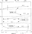
Fig. 2 is resulting at the figure of the bottom of large ratio of height to width path titanium thickness to sputtering pressure according to the present invention.
Fig. 3 is the bar graph of titanium deposition rate as the function of collimation depth-width ratio.
With reference to Fig. 1, showed a substrate 10 that has diffusion zone 20 thereon among the figure, conductor 40 of the present invention is deposited in the hole 50 in the passivation layer 30 among the figure.The thickness H of 30 deposits of passivation layer of boron-phosphorosilicate glass (BPSG) or phosphorosilicate glass (PSG) is approximately the 11K dust.Contact hole 50 passes BPSG or PSG30 forms, and diffusion zone 20 is exposed.Therefore about 5000 dusts of the width W of contact hole 50, spread the depth-width ratio H of contact hole: W is approximately 2: 1.
In the present invention, layer 40 forms by collimator 60 active sputters from sputtering target 70.Collimator 60 is placed on one perpendicular on the contact hole planar plane, preferably also is parallel to sputtering target 70.Collimator 60 is the thick steel plate of 1cm or the plate of other materials that can not soften or be out of shape under following sputter state, has opened many adjacent holes above.These holes are arranged in cellular pattern." the Lift-off Magnetron SputterDeposition " that is writing by people such as S.M.Rossnagel with the example of the material (copper) of collimator deposit sputter, American Vacuum Society 36th NationalSymposium, Boston Mass, October 23-27,1989, P.286, provide in FinalProgram " is deposited on the structural copper of emission (lift-off) the to eliminate the sidewall deposit " literary composition, in addition, at United States Patent (USP) 4 by Rossnagel, also have in 824,544.
The effect of collimator is the path of limit injection, makes material to incide on the substrate surface near vertical angle.Not to be deposited on the collimator surface, perhaps in the hole of collimator near vertical angle incident material.Line SA-SE shown in Fig. 1 represents from the jet path of the atom of target 70 ejaculations.Atom along path SA, SB and SE injection all is deposited on the substrate by collimator aperture.Atom along path SC and SD is a non-normal incidence, therefore can not pass through collimator.
In general, the result by the collimator sputter is: the situation when not having collimator is compared, and in the layer 40 that forms, the per-cent of thickness of part 40A that the thickness of the part 40c of contact hole bottom accounts for the passivation layer upper surface is higher.Also have, as what will go through later on, the weave construction of resulting film, contact resistance and other characteristics all are better than in some aspects with the resulting characteristic of conventional sputtering method.At last, the material 40B thickness that is deposited on the sidewall of contact hole is very even, does not have the coating thickening phenomenon that has in the conventional sputtering technology on the top of contact hole sidewall.
The result who utilizes sputtered titanium, titanium nitride and sputtered with Ti/various tests that the TiN lamination is realized below will be discussed.1. sputter titanium nitride.
In battery of tests, with the method for sputter in 150 ℃ of nitrogen environments on silicon-dioxide deposit one deck titanium nitride film, unique here variable collimator that is to use.The distribution of the concentration of oxygen on the degree of depth records with Electron Spectroscopic Chemical Analysis (ESCA) in the film.TiN surface oxygen content by the collimator sputter is approximately 30%.This is because the oxygen around the initial stage absorbing when deposition unit is taken out sample causes.TiN thickness initial 1/10 in the per-cent of oxygen drop to below 1%, remaining film keeps this value always.The TiN layer of sputter during for collimator of no use, the oxygen level of beginning is 30% equally, but with in the TiN oxygen level that obtains by collimator is reduced to identical 1/10 thickness below 1%, can only drop to the oxygen level of about 6-8% when not having collimator.The oxygen level that about 6-8% is not all arranged by the TiN layer of collimator sputter in addition.This result shows that the film that obtains with the collimator deposit is more finer and closely woven than the film that obtains without the collimator deposit, and oxygen contamination is also less after the deposit.Should be noted that low oxygen content is very important, because this can make the formation of titanium oxide reduce to minimum, titanium oxide can make resistivity degenerate, and the adhesion characteristics of film is reduced.
In other a series of tests, can confirm above this point, in these trials, record through collimation with without the situation of body resistivity of collimation deposited film.It is the test result of the TiN layer of the given thickness that forms on 125mm or the 200mm silicon chip that last appended table has shown at diameter, and has pointed out that deposition temperature and environment are (as being designated as " Ar/N in the argon of equivalent and nitrogen
2", in the pure nitrogen gas environment, then be designated as " N
2").Speech " central authorities " and " edge " expression are near the zone (central authorities are for the edge) of silicon chip, from reading test data here.It no matter is the silicon chip of 125mm diameter or the silicon chip of 200mm diameter does not influence the result.The result under the identical situation of every other condition, adds collimator and can make body resistivity reduce 3 times (at 150 ℃ of pure N at least as can be seen from table
2In the result that records of the sheet edge of deposit be 102 μ Ω-cm to 305 μ Ω-cm, surveying in sheet central authorities is 124 pairs 1180 (almost little 10 times); At about 500 ℃ of pure N
2It is 90 pairs 640 (little 6 times) that the central authorities of the sheet of middle deposit survey).This body resistivity that reduces has significantly been used the less explanation of oxygen level not, but owing to the microstructure of film tightr (nonconducting space is still less promptly arranged).
In another group test, TiN sputtering technology deposit, whether variable just collimates, and by the SEM microgram film of cutting open is analyzed.Can find, show very fine and closely woven weave construction, lack with regard to the TiN film of intercrystalline space than sputter without collimation through the TiN film of collimation.In addition, this film has high cylindrical crystalline-granular texture.This very fine and closely woven weave construction is reducing to have played crucial effect aspect the body resistivity; In addition, since the intercrystalline space reduce can reduce the infiltration of oxygen in the film and provide one deck the anti-saturating blocking layer of reaction by-product infiltration by the CVD process.2. sputtered titanium
Use collimator deposit titanium can obtain similar result.That is exactly that the titanium behind the collimation presents lower oxygen impurity concentration, lower body resistivity and more regular weave construction.
Additional analysis has illustrated the situation that the plating material quantity of contact hole bottom increases.Fig. 2 shows to have depth-width ratio and is about 2: 1 the thickness (as the per-cent of the thickness of passivation layer upper surface titanium) of bottom titanium of a contact hole to the relation of sputtering pressure.The thickness of the titanium film of the contact hole bottom that as can be seen from the figure, obtains without collimation only is about 5% of passivation layer upper surface titanium film thickness in whole sputtering pressure scope.
Note that when using collimator when deposition temperature increases and the depth-width ratio of collimator when strengthening, thickness is than also along with raising.Temperature during the deposit titanium plays an important role to the thickness of bottom film.The depth-width ratio of collimator is 1: 1 o'clock, and deposition temperature is elevated to 500 ℃, thickness of coating per-cent raising 7% from 150 ℃.The depth-width ratio of collimator is 2: 1 o'clock, and temperature rises to 500 ℃ from 150 ℃, when pressure is low, and the double thickness of film, per-cent increases by 10% when sputtering pressure is higher.This phenomenon does not exist the titanium layer that does not have the collimator sputter; Improving temperature makes the thickness increase of contact hole bottom film very limited.In addition, the straight titanium nitride of this phenomenon misalignment does not exist yet; Deposit TiN does not increase the thickness of how many contact hole bottom film under higher temperature.
Increase the depth-width ratio of collimator and increase between the per-cent of plating material that is deposited on the contact hole bottom and have direct relation with respect to top plating material.Do not consider variation of temperature (just only considering the situation of 150 ℃ of deposits shown in Fig. 2), and the data of considering sputter pressure are 0.12Pa, can see: to not adding the situation of collimation, per-cent is about 4%, it for the collimator depth-width ratio 1: 1 situation, per-cent is 11%, is 2: 1 situation for the collimator depth-width ratio, and per-cent is 17% (being uncollimated 4 times).Because at N
2Or N
2The situation of titanizing is similar in the/Ar environment, therefore is expected to obtain similar result for titanium nitride.
The contriver finds that this increase of depth-width ratio makes the quantity of material of institute's deposit in the unit time calculate 4 times of minimizings roughly.As shown in Figure 3, when with 1: 1 collimator with compare deposition rate without collimator and significantly reduce, from 1: 1 collimator to 2: 1 collimator then deposition rate reduce by 4 times.With reference to figure 1, along with the depth-width ratio of collimator increases, the per-cent of the atom that sprays along path SC will increase, and therefore, less atom can be used for deposit.Simultaneously, the atom by collimator is with the less angle incident in relative contact hole plane.In other words, increased along the per-cent of the atom of path SB, SE, therefore, the per-cent that arrives the atom of contact hole bottom has increased.
The contriver finds that also deposit per-cent does not increase for little depth-width ratio contact hole.For little depth-width ratio contact hole, the effect of a collimator of 2: 1 unlike a collimator of 1: 1 well what.Therefore, the contriver advocates to take optimal compromise between deposition rate and the increase deposit of contact hole bottom, and promptly the depth-width ratio of collimator holes is not more than the depth-width ratio of contact hole.
Found can reduce TiSi at the titanium that the bottom increased in large ratio of height to width hole
2The resistance of silicon compound electrode.Reduce the silicide ultimate resistance at the dark Kong Zhongjing of 0.8 μ m collimation deposit (depth-width ratio is 1.5: 1) titanium greatly with comparing without the collimation situation.Along with the increase of aperture depth-width ratio, resistance just reduction/stability increases.3. sputtered with Ti/TiN lamination
Above-mentioned conclusion about Ti and TiN Overlay can occur if combine.Carried out some tests, in test, by depth-width ratio be 2: 1 or bigger contact hole in succession the TiN of the titanium of sputter 600 dusts and 400 dusts so that contact with the p spreading area with the n spreading area that separates.Then, contact hole fills up with equal thick CVD tungsten, utilizes the two dimension (Planarization) of standard to handle and forms the tungsten terminal stud, and this contact hole that is filled interconnects with aluminum steel.For uncollimated Ti/TiN, average contact resistance is: to N
+The contact is 71 Ω/every contact, to P
+The contact is 138 Ω/every contact.For Ti/TiN, to N through collimation
+And P
+The contact contact resistance all is about 1 Ω/every contact.Compare by the collimator sputter and greatly reduce contact resistance in addition, with without the collimation deposit.We think that this reducing of contact resistance is the additional effect that is deposited on the titanium of contact hole bottom.In addition, through the finer and closely woven characteristic of TiN barrier film of collimation in CVD tungsten deposition process, prevented fluorine be penetrated into below in the titanium layer.
We have discussed with the resulting various test-results of collimator sputter, and concrete sputter procedure itself will be discussed now.General processing is similar to conventional sputtering method.The gaseous plasma that produces inert atom (for example argon) removes the bombarding cathode target, knocking-only is deposited on the electric isolated on-chip atom of.In the example of titanium nitride, form the group weight form of titanium nitride deposit with nitrogen as the bombardment source with the titanium atom reaction without argon in the system, thereby can obtain processing controls preferably.
The atom that sprays can suffer the scattering and the bump of plasma (work) gas atom (for example argon), thereby leave straight line (off-line) by after the collimator.Therefore, in order to reduce scattering, it is very important using low operating air pressure (less than 0.13 handkerchief (1.0 milli torr)) when by the collimator deposit.The composition of working gas also influences scattering.Ar atmo cause injection atom to depart from departing from of wanting low weight working gas for example nitrogen caused bigger.Purity nitrogen is the preferred working gas with collimator deposit TiN.Use purity nitrogen to guarantee that (even with collimator the time required low pressure situation) has enough nitrogen formation TiN.Owing to will clash into titanium atom from sputtering source, lighter N
2Atom is ineffective, and therefore, cathode power just must the 3-6KV from argon the time be increased to uses N
2The time 6-9KW.
These tests with the TiN deposit cause some about how making several conclusions of gas scattering minimum.Even a conclusion is also to use lighter inert atom when sputtered titanium.Another conclusion is (to be lower than common 0.4-0.5 handkerchief (3-4 milli torr) with lower sputter pressure; Generally be lower than 0.13 handkerchief (1.0 milli torr)), even when using argon, also be like this as the inertia sputtering material.
Discuss, put up with now and fill up object lesson of contact hole discussion shown in Figure 1 with regard to all respects of the present invention.Limit and deposit spreading area 20 and passivation layer 30 with routine techniques.Then, on passivation layer 30, limit the photoresist mask, limit contact hole 50, utilize active ion technique at CF
4+ O
2Etch contact hole in the environment.It should be noted that the photosensitive resin mask is very thick, thus when etching finishes image also in the original place.
Then, under 0.09-0.13 handkerchief (0.7-1.0 milli torr) pressure, pass through the titanium of collimator sputtering deposit 600 dusts of 1: 1 and the TiN of 400 dusts.During the deposit titanium, substrate temperature remains on 450 ℃ and bombard atom with argon as inertia.During deposit TiN, argon is changed into nitrogen.Resulting synthetic film has the 40c part (see figure 1) that is about 260 dusts (be about 40 angstroms portion thickness 25%).In addition, closing film forming sidewall sections 40B, is uniformly along the whole sidewall thickness of contact hole basically, the adhesive power of the film that has added after this has strengthened.As mentioned above, resulting film with compare without the similar film of collimation deposit have low body resistivity, low contact resistance, low oxygen level and strengthened surface microstructure.In addition, make moderate progress through the fluorine infiltration of the TiN film of collimation deposit to the lower membrane that stops contact hole bottom.Know that the fluorine impurity of lower floor's titanium film and silicide are to damage some mechanical propertys reason of (comprise the adhesion loss of CVD tungsten and increase contact resistance).To some application, can be by 500 ℃-600 ℃ at N
2Anneal in the environment and make remaining titanium on the sidewall change the fluorine barrier properties of TiN enhancement layer into.
Can make various modifications to said structure and principle, but not break away from the spirit and scope of the present invention.For example, though the present invention is that example is described with titanium and titanium nitride, the present invention can be used for any other sputter, active sputter or the blocking material (as chromium, tungsten and TiW) of evaporation plating and the material (as tungsten and aluminium) that is used for filling up high aspect ratio apertures.In addition, though the present invention is described with specific contact embodiment, the present invention can be applicable to the very big range of application of wanting plating or filling up high aspect ratio apertures.At last, for a kind of given applicable cases, the concrete time of being discussed, temperature, pressure, surrounding environment etc. can optimizings.
Body resistance counting rate meter according to the formed titanium nitride layer of the present invention
| Film sample | Grain-size (NM) | Thickness (NM) | K body resistivity (uOHM-CM) |
| 200mm,150C.,Ar/N 2Central authorities | 6-15 | ?61 | ?866 |
| 200mm,150C.,Ar/N 2The edge | 4-10 | ?62 | ?306 |
| 200mm, 150C. has only N 2Central authorities | 7-17 | ?66 | ?1180 |
| 200mm, 150C. has only N 2The edge | 6-10 | ?73 | ?305 |
| 125mm, 150C. has only N 2Central authorities are through collimation | <10 | ?59 | ?124 |
| 125mm, 150C. has only N 2The edge is through collimation | <10 | ?61 | ?102 |
| 200mm,500C.,Ar/N 2The edge | 5-16 | ?58 | ?560 |
| 200mm,500C.,Ar/N 2The edge | 4-12 | ?64 | ?205 |
| 200mm, 500C. has only N 2Central authorities | 6-15 | ?63 | ?640 |
| 200mm, 500C. has only N 2The edge | 5-15 | ?75 | ?190 |
| 125mm, 450C. has only N 2Central authorities are through collimation | <10 | ?60 | ?90 |
Claims (18)
1. the method for deposit layer of conductive material on substrate, the contoured surface of this substrate comprises the pit that at least one depth-width ratio was at least 1: 1, described method is characterised in that:
Before being deposited on the described substrate, the atom of described electro-conductive material was about 1: 1 by a depth-width ratio or the bigger straight device of heap.
2. the method for claim 1 is characterized in that:
Described substrate is an integrated circuit substrate, and it has a plurality of holes in the sealing coat of establishing thereon, and described a plurality of holes have at the bottom of sidewall and one, described a plurality of holes certain a fewly has a depth-width ratio 1: 1 or bigger at least; And
Described electro-conductive material is deposited on the described sealing coat and the described sidewall in described a plurality of holes wherein and at the described end.
3. the method for claim 2 is characterized in that:
Described electro-conductive material is splashed on the described sealing coat by described collimator; And
Described sputter step is to carry out being lower than under the pressure of 0.4Pa.
4. the method for claim 3 is characterized in that: certain a few depth-width ratio with 2: 1 at least in described hole.
5. the method for claim 3, it is characterized in that: described electro-conductive material comprises titanium.
6. the method for claim 3, it is characterized in that: described electro-conductive material comprises titanium nitride.
7. the method for claim 6, it is characterized in that: described sputter step is at N
2Carry out in the environment.
8. the method for claim 1 is characterized in that:
Described on described substrate the deposit layer of conductive material be blocking layer metallurgy to be splashed in the contact hole that is arranged on defined in the on-chip isolated body certain a few depth-width ratio that have more than or equal to 2: 1 at least of described contact hole; And
A collimator is arranged on the described substrate, and this collimator has the opening that some depth-width ratio was at least 1: 1 at least.
9. the method for claim 1 is characterized in that:
Described substrate is an integrated circuit substrate, and it has the hole of large ratio of height to width in the sealing coat of establishing thereon, and described electro-conductive material is refractory metal or high melting point metal alloy; And
Described refractory metal or high melting point metal alloy are that the collimator by 1: 1 depth-width ratio is splashed on the described sealing coat under the pressure of 0.4Pa being lower than.
10. the method for claim 9, it is characterized in that: the described large ratio of height to width in the described hole in the described sealing coat is 2: 1 at least.
11. the method for claim 9 is characterized in that: described refractory metal is sputter under the pressure that is lower than 0.13 pascal.
12. the method for claim 9 is characterized in that: described refractory metal comprises titanium.
13. the method for claim 9 is characterized in that: described high melting point metal alloy comprises titanium nitride.
14. the method for claim 13 is characterized in that: described sputter is at N
2Carry out under the environment.
15. the method for claim 1 is characterized in that:
Described is that pit inner conducting layer with large ratio of height to width is splashed on the surface of integrated circuit substrate in deposit layer of conductive material on the described substrate;
Described collimator is arranged on the described integrated circuit substrate; And
Described sputter step is to carry out under pressure is lower than the condition of 0.4Pa.
16. the method for claim 15 is characterized in that: described sputter step is to carry out being lower than under the pressure of 0.13Pa.
17. the method for claim 1 is characterized in that:
Described conductive material layer is the blocking layer, and described pit is the hole that comprises upper side wall; And
Described blocking layer is sputter under the condition that improves the deposit of material in described hole.
18. the method for claim 1 is characterized in that:
Described conductive material layer is the Ti/TiN blocking layer, and described pit is formed hole in the passivation layer that is provided with on substrate;
By a collimator one deck titanium is splashed on the described substrate with 1: 1 depth-width ratio opening; And
By described collimator one deck titanium nitride is splashed on the described titanium layer, described second sputter step is at sufficient N
2Carry out under the compression ring border.
Applications Claiming Priority (3)
| Application Number | Priority Date | Filing Date | Title |
|---|---|---|---|
| US69017191A | 1991-04-19 | 1991-04-19 | |
| US07/690,171 | 1991-04-19 | ||
| US690,171 | 1991-04-19 |
Publications (2)
| Publication Number | Publication Date |
|---|---|
| CN1065888A CN1065888A (en) | 1992-11-04 |
| CN1033175C true CN1033175C (en) | 1996-10-30 |
Family
ID=24771386
Family Applications (1)
| Application Number | Title | Priority Date | Filing Date |
|---|---|---|---|
| CN92101844A Expired - Lifetime CN1033175C (en) | 1991-04-19 | 1992-03-19 | Method of depositing conductors in high aspect ratio apertures |
Country Status (10)
| Country | Link |
|---|---|
| US (1) | US5401675A (en) |
| EP (1) | EP0509305A1 (en) |
| JP (1) | JP2726595B2 (en) |
| KR (1) | KR960011927B1 (en) |
| CN (1) | CN1033175C (en) |
| BR (1) | BR9201351A (en) |
| CA (1) | CA2061119C (en) |
| MY (1) | MY108408A (en) |
| SG (1) | SG42979A1 (en) |
| TW (1) | TW207029B (en) |
Families Citing this family (40)
| Publication number | Priority date | Publication date | Assignee | Title |
|---|---|---|---|---|
| US6521106B1 (en) | 1990-01-29 | 2003-02-18 | Novellus Systems, Inc. | Collimated deposition apparatus |
| US5300813A (en) * | 1992-02-26 | 1994-04-05 | International Business Machines Corporation | Refractory metal capped low resistivity metal conductor lines and vias |
| CA2111536A1 (en) * | 1992-12-16 | 1994-06-17 | Geri M. Actor | Collimated deposition apparatus |
| KR970001883B1 (en) * | 1992-12-30 | 1997-02-18 | 삼성전자 주식회사 | Semiconductor device and method for manufacturing the same |
| TW271490B (en) * | 1993-05-05 | 1996-03-01 | Varian Associates | |
| US5346601A (en) * | 1993-05-11 | 1994-09-13 | Andrew Barada | Sputter coating collimator with integral reactive gas distribution |
| DE4325051C1 (en) * | 1993-07-26 | 1994-07-07 | Siemens Ag | Arrangement for depositing a layer on a substrate wafer by sputtering and method for its operation |
| JP2699839B2 (en) * | 1993-12-03 | 1998-01-19 | 日本電気株式会社 | Method for manufacturing semiconductor device |
| US5711858A (en) * | 1994-04-12 | 1998-01-27 | International Business Machines Corporation | Process for depositing a conductive thin film upon an integrated circuit substrate |
| US5633189A (en) * | 1994-08-01 | 1997-05-27 | Actel Corporation | Method of making metal to metal antifuse |
| EP0793268A3 (en) * | 1995-05-23 | 1999-03-03 | Texas Instruments Incorporated | Process for filling a cavity in a semiconductor device |
| TW298674B (en) * | 1995-07-07 | 1997-02-21 | At & T Corp | |
| JPH0936228A (en) * | 1995-07-21 | 1997-02-07 | Sony Corp | Formation of wiring |
| US5700716A (en) | 1996-02-23 | 1997-12-23 | Micron Technology, Inc. | Method for forming low contact resistance contacts, vias, and plugs with diffusion barriers |
| US5895266A (en) * | 1996-02-26 | 1999-04-20 | Applied Materials, Inc. | Titanium nitride barrier layers |
| DE19621855C2 (en) * | 1996-05-31 | 2003-03-27 | Univ Dresden Tech | Process for producing metallizations on semiconductor bodies using a pulsed vacuum arc evaporator |
| US5956612A (en) * | 1996-08-09 | 1999-09-21 | Micron Technology, Inc. | Trench/hole fill processes for semiconductor fabrication |
| US6025269A (en) * | 1996-10-15 | 2000-02-15 | Micron Technology, Inc. | Method for depositioning a substantially void-free aluminum film over a refractory metal nitride layer |
| US6045634A (en) * | 1997-08-14 | 2000-04-04 | Praxair S. T. Technology, Inc. | High purity titanium sputtering target and method of making |
| TW430900B (en) * | 1997-09-08 | 2001-04-21 | Siemens Ag | Method for producing structures having a high aspect ratio |
| US6287436B1 (en) | 1998-02-27 | 2001-09-11 | Innovent, Inc. | Brazed honeycomb collimator |
| US6362097B1 (en) | 1998-07-14 | 2002-03-26 | Applied Komatsu Technlology, Inc. | Collimated sputtering of semiconductor and other films |
| US6140217A (en) * | 1998-07-16 | 2000-10-31 | International Business Machines Corporation | Technique for extending the limits of photolithography |
| US6197684B1 (en) * | 1999-03-19 | 2001-03-06 | United Microelectronics Corp. | Method for forming metal/metal nitride layer |
| US6342133B2 (en) | 2000-03-14 | 2002-01-29 | Novellus Systems, Inc. | PVD deposition of titanium and titanium nitride layers in the same chamber without use of a collimator or a shutter |
| ATE335868T1 (en) * | 2002-03-19 | 2006-09-15 | Scheuten Glasgroep Bv | DEVICE AND METHOD FOR DIRECTED APPLICATION OF DEPOSITION MATERIAL TO A SUBSTRATE |
| KR100528069B1 (en) * | 2003-09-02 | 2005-11-15 | 동부아남반도체 주식회사 | Semiconductor Device And Method For Manufacturing The Same |
| KR100561523B1 (en) * | 2003-12-31 | 2006-03-16 | 동부아남반도체 주식회사 | Method for forming Al interconnect |
| KR100628242B1 (en) * | 2004-06-24 | 2006-09-26 | 동부일렉트로닉스 주식회사 | Method for fabricating barrier layer of semiconductor device |
| KR100602087B1 (en) * | 2004-07-09 | 2006-07-14 | 동부일렉트로닉스 주식회사 | Semiconductor device and method of manufacturing the same |
| KR100552857B1 (en) * | 2004-10-25 | 2006-02-22 | 동부아남반도체 주식회사 | Method for fabricating contact of semiconductor device |
| US8236691B2 (en) * | 2008-12-31 | 2012-08-07 | Micron Technology, Inc. | Method of high aspect ratio plug fill |
| JP6088083B1 (en) * | 2016-03-14 | 2017-03-01 | 株式会社東芝 | Processing device and collimator |
| USD858468S1 (en) * | 2018-03-16 | 2019-09-03 | Applied Materials, Inc. | Collimator for a physical vapor deposition chamber |
| USD859333S1 (en) * | 2018-03-16 | 2019-09-10 | Applied Materials, Inc. | Collimator for a physical vapor deposition chamber |
| USD937329S1 (en) | 2020-03-23 | 2021-11-30 | Applied Materials, Inc. | Sputter target for a physical vapor deposition chamber |
| USD998575S1 (en) | 2020-04-07 | 2023-09-12 | Applied Materials, Inc. | Collimator for use in a physical vapor deposition (PVD) chamber |
| USD1009816S1 (en) | 2021-08-29 | 2024-01-02 | Applied Materials, Inc. | Collimator for a physical vapor deposition chamber |
| USD997111S1 (en) | 2021-12-15 | 2023-08-29 | Applied Materials, Inc. | Collimator for use in a physical vapor deposition (PVD) chamber |
| USD1038901S1 (en) | 2022-01-12 | 2024-08-13 | Applied Materials, Inc. | Collimator for a physical vapor deposition chamber |
Family Cites Families (23)
| Publication number | Priority date | Publication date | Assignee | Title |
|---|---|---|---|---|
| CH611938A5 (en) * | 1976-05-19 | 1979-06-29 | Battelle Memorial Institute | |
| DE2705225C2 (en) * | 1976-06-07 | 1983-03-24 | Nobuo Tokyo Nishida | Ornamental part for clocks etc. |
| US4293374A (en) * | 1980-03-10 | 1981-10-06 | International Business Machines Corporation | High aspect ratio, high resolution mask fabrication |
| KR900001825B1 (en) * | 1984-11-14 | 1990-03-24 | 가부시끼가이샤 히다찌세이사꾸쇼 | Sputtering apparatus with film forming directivity |
| FR2583220B1 (en) * | 1985-06-11 | 1987-08-07 | Thomson Csf | PROCESS FOR PRODUCING AT LEAST TWO METALLIZATIONS OF A SEMICONDUCTOR COMPONENT COVERED WITH A DIELECTRIC LAYER AND COMPONENT OBTAINED BY THIS DIELECTRIC |
| JPS627855A (en) * | 1985-07-05 | 1987-01-14 | Hitachi Ltd | Sputtering device |
| JPS6217173A (en) * | 1985-07-15 | 1987-01-26 | Ulvac Corp | Flat plate magnetron sputtering device |
| JPH084088B2 (en) * | 1986-02-27 | 1996-01-17 | 工業技術院長 | Thin film formation method |
| US4849079A (en) * | 1986-05-23 | 1989-07-18 | International Business Machines Corp. | Process for preparing low electrical contact resistance composition |
| US4756810A (en) * | 1986-12-04 | 1988-07-12 | Machine Technology, Inc. | Deposition and planarizing methods and apparatus |
| US4783248A (en) * | 1987-02-10 | 1988-11-08 | Siemens Aktiengesellschaft | Method for the production of a titanium/titanium nitride double layer |
| JPH0660391B2 (en) * | 1987-06-11 | 1994-08-10 | 日電アネルバ株式会社 | Sputtering equipment |
| US4824544A (en) * | 1987-10-29 | 1989-04-25 | International Business Machines Corporation | Large area cathode lift-off sputter deposition device |
| US4962414A (en) * | 1988-02-11 | 1990-10-09 | Sgs-Thomson Microelectronics, Inc. | Method for forming a contact VIA |
| JP2776826B2 (en) * | 1988-04-15 | 1998-07-16 | 株式会社日立製作所 | Semiconductor device and manufacturing method thereof |
| US4822753A (en) * | 1988-05-09 | 1989-04-18 | Motorola, Inc. | Method for making a w/tin contact |
| US5112693A (en) * | 1988-10-03 | 1992-05-12 | Ppg Industries, Inc. | Low reflectance, highly saturated colored coating for monolithic glazing |
| JPH02143521A (en) * | 1988-11-25 | 1990-06-01 | Tokyo Electron Ltd | Sputtering method |
| JP2768364B2 (en) * | 1989-03-16 | 1998-06-25 | 富士通株式会社 | Method for manufacturing semiconductor device |
| US4920073A (en) * | 1989-05-11 | 1990-04-24 | Texas Instruments, Incorporated | Selective silicidation process using a titanium nitride protective layer |
| US4994162A (en) * | 1989-09-29 | 1991-02-19 | Materials Research Corporation | Planarization method |
| US5026470A (en) * | 1989-12-19 | 1991-06-25 | International Business Machines | Sputtering apparatus |
| US5008217A (en) * | 1990-06-08 | 1991-04-16 | At&T Bell Laboratories | Process for fabricating integrated circuits having shallow junctions |
-
1992
- 1992-02-12 CA CA002061119A patent/CA2061119C/en not_active Expired - Fee Related
- 1992-02-28 TW TW081101510A patent/TW207029B/zh active
- 1992-03-19 MY MYPI92000456A patent/MY108408A/en unknown
- 1992-03-19 KR KR1019920004506A patent/KR960011927B1/en not_active IP Right Cessation
- 1992-03-19 CN CN92101844A patent/CN1033175C/en not_active Expired - Lifetime
- 1992-03-31 EP EP92105501A patent/EP0509305A1/en not_active Withdrawn
- 1992-03-31 SG SG1996001715A patent/SG42979A1/en unknown
- 1992-04-09 JP JP4088645A patent/JP2726595B2/en not_active Expired - Lifetime
- 1992-04-13 BR BR929201351A patent/BR9201351A/en not_active IP Right Cessation
-
1993
- 1993-03-24 US US08/036,224 patent/US5401675A/en not_active Expired - Lifetime
Also Published As
| Publication number | Publication date |
|---|---|
| EP0509305A1 (en) | 1992-10-21 |
| CA2061119A1 (en) | 1992-10-20 |
| TW207029B (en) | 1993-06-01 |
| KR960011927B1 (en) | 1996-09-04 |
| SG42979A1 (en) | 1997-10-17 |
| JPH05299375A (en) | 1993-11-12 |
| CN1065888A (en) | 1992-11-04 |
| JP2726595B2 (en) | 1998-03-11 |
| BR9201351A (en) | 1992-12-01 |
| US5401675A (en) | 1995-03-28 |
| CA2061119C (en) | 1998-02-03 |
| KR920020613A (en) | 1992-11-21 |
| MY108408A (en) | 1996-09-30 |
Similar Documents
| Publication | Publication Date | Title |
|---|---|---|
| CN1033175C (en) | Method of depositing conductors in high aspect ratio apertures | |
| JP2725944B2 (en) | Metal layer deposition method | |
| EP0875924A2 (en) | Improved tantalum-containing barrier layers for copper | |
| CN1708846A (en) | A method for depositing a metal layer on a semiconductor interconnect structure having a capping layer | |
| JP3353727B2 (en) | Method for forming wiring structure of semiconductor device | |
| CN1120241A (en) | Refractory metal capped low resistivity metal conductor lines and vias formed using PVD and CVD | |
| US5918150A (en) | Method for a chemical vapor deposition of copper on an ion prepared conductive surface | |
| JP2951636B2 (en) | Method for manufacturing a metallization structure | |
| US6087726A (en) | Metal interconnect stack for integrated circuit structure | |
| CN1601702A (en) | In-situ metal barrier deposition of sputter etching on interconnect structure | |
| KR100365061B1 (en) | Semiconductor device and semiconductor device manufacturing method | |
| JP2001053026A (en) | Manufacture of semiconductor device | |
| CN1913125A (en) | Via bottom contact and method of manufacturing same | |
| JP2000091266A (en) | Method for improvement of aluminum metallized structure for tungsten etch back process | |
| US6245668B1 (en) | Sputtered tungsten diffusion barrier for improved interconnect robustness | |
| JP3732010B2 (en) | Method for depositing low resistivity titanium oxynitride (TiON) film that gives excellent texture to the conductor layer deposited in a later step | |
| KR100633685B1 (en) | Metalizing method of semiconductor device | |
| JPH04242960A (en) | Wiring of integrated circuit | |
| CN1207763C (en) | Graded barrier of metal line copper back end | |
| CN1405845A (en) | Method for manufacturing titanium oxide layer | |
| JPH07169834A (en) | Method for embedding interlayer connecting hole | |
| JPH04324636A (en) | Semiconductor device and its manufacture | |
| JPH1079358A (en) | Sputtering method | |
| JP2943029B2 (en) | Method of manufacturing semiconductor device for forming multilayer wiring | |
| CN1477694A (en) | Method for making mesolayer window |
Legal Events
| Date | Code | Title | Description |
|---|---|---|---|
| C10 | Entry into substantive examination | ||
| SE01 | Entry into force of request for substantive examination | ||
| C06 | Publication | ||
| PB01 | Publication | ||
| C14 | Grant of patent or utility model | ||
| GR01 | Patent grant | ||
| C15 | Extension of patent right duration from 15 to 20 years for appl. with date before 31.12.1992 and still valid on 11.12.2001 (patent law change 1993) | ||
| OR01 | Other related matters | ||
| C17 | Cessation of patent right | ||
| CX01 | Expiry of patent term |
Expiration termination date: 20120319 Granted publication date: 19961030 |