CN103295478A - Video display device and illuminating device - Google Patents
Video display device and illuminating device Download PDFInfo
- Publication number
- CN103295478A CN103295478A CN2013100063839A CN201310006383A CN103295478A CN 103295478 A CN103295478 A CN 103295478A CN 2013100063839 A CN2013100063839 A CN 2013100063839A CN 201310006383 A CN201310006383 A CN 201310006383A CN 103295478 A CN103295478 A CN 103295478A
- Authority
- CN
- China
- Prior art keywords
- circuit board
- illuminator
- video display
- display devices
- light
- Prior art date
- Legal status (The legal status is an assumption and is not a legal conclusion. Google has not performed a legal analysis and makes no representation as to the accuracy of the status listed.)
- Pending
Links
Images


Abstract
The invention discloses a video display device and an illuminating device. According to one embodiment, the video display device comprises a shell body, a display device, illuminating devices, components, controllers, and circuit boards, wherein the display device comprises a screen, at least a part of the display device is accommodated in the shell body, each illuminating device is configured in such a way that light is emitted onto the display device, each component is configured in such a way that the component switches between a state of supplying electric power to each illuminating device and a state of not supplying the electric power to each illuminating device. Each controller is configured as a control component which switches between a state of supplying the electric power through the components and a state of not supplying the electric power. Each circuit board comprises a first surface and a second surface which is opposite to the first surface, and each circuit board is provided with the illuminating devices and the components.
Description
The cross reference of related application
The application based on and require the rights and interests of the right of priority of the Japanese patent application No.2012-044520 that submitted on February 29th, 2012, its full content is incorporated into this by quoting as proof.
Technical field
The embodiment of Miao Shuing relates generally to a kind of video display devices and light-emitting device herein.
Background technology
Usually, known a kind of liquid crystal indicator, this liquid crystal indicator comprises: the light guide plate that is arranged on the rear side of display; And a plurality of light emitting diodes (LED) that are used for backlight, these light emitting diodes are created in the light that transmits in the light guide plate.
In this device, expect more effectively arrangement component.
Summary of the invention
Therefore, according to an embodiment of the invention, as an example, one of purpose is image display device and the light-emitting device that obtains a kind of more effectively arrangement component.
According to an embodiment, video display devices comprises: housing; Display; Illuminator; Element; Controller; And circuit board.Display comprises screen.At this, the part of display is contained in the housing at least.Illuminator is configured to light is transmitted on the display.Element is configured to switch supplying power to illuminator and be not supplied between the illuminator.Controller is configured to control element, to switch between by component feeding electric power and non-supply capability.Circuit board comprise first surface and with the first surface opposing second surface, and be provided with illuminator and element.
According to the video display devices of above-mentioned structure, degree of freedom that can the layout of reinforcing member in video display devices.
Description of drawings
The general structure of implementing a plurality of features of the present invention is described now with reference to accompanying drawing.Provide accompanying drawing and relevant description, embodiments of the present invention to be described and not to limit scope of the present invention.
Fig. 1 is the exemplary front view according to the video display devices of an embodiment;
Fig. 2 is the exemplary side elevation of the video display devices in this embodiment;
Fig. 3 is the exemplary signal exploded perspective view of the housing of the video display devices in this embodiment;
Fig. 4 is the illustrative diagram of the light-emitting device of the circuit structure of control circuit and the video display devices in this embodiment;
Fig. 5 is the exemplary plan view of the light-emitting device in the video display devices that comprises in this embodiment;
Fig. 6 is the exemplary cross-sectional of the part of the light-emitting device of the line VI-VI intercepting in Fig. 5 in this embodiment and housing;
Fig. 7 is the exemplary cross-sectional that is included in the part of light-emitting device in the video display devices according to first modification of this embodiment (at the cross-sectional view of the position intercepting identical with the position among Fig. 6) and housing;
Fig. 8 is the exemplary plan view that is included in according to the light-emitting device in the video display devices of second modification of this embodiment;
Fig. 9 is the exemplary cross-sectional of the line IX-IX intercepting among Fig. 8 in second modification;
Figure 10 is the exemplary plan view that is included in according to the light-emitting device in the video display devices of the 3rd modification of this embodiment;
Figure 11 is the exemplary cross-sectional of the line XI-XI intercepting among Figure 10 in the 3rd modification;
Figure 12 is the exemplary plan view that is included in according to the light-emitting device in the video display devices of the 4th modification of this embodiment; And
Figure 13 is the exemplary plan view that is included in according to the light-emitting device in the video display devices of the 5th modification of this embodiment.
Embodiment
Following illustrative embodiment and modification comprise the element of like configurations.Therefore, hereinafter, the element of like configurations represents with common Reference numeral, and partly omits the repeat specification to it.In this embodiment and modification in parts can be replaced by the corresponding component in other embodiment and the modification.In addition, limit unless have in addition especially, it is identical with in other embodiment these to be included in the structure, position etc. of the parts in this embodiment and the modification.
In addition, for convenience's sake, define direction in some drawings.When watching indicator screen from the front side, directions X points to right (when watching indicator screen from rear side, pointing to a left side), and on Y-direction is pointed to, and the Z direction is on the direction of normal of indicator screen.
In addition, in below the embodiment and modification, video display devices is configured to television receiver.Yet, be not limited thereto according to the video display devices of this embodiment.Video display devices according to this embodiment can be configured to comprise the various electronic installations with display backlight, such as PC, smart mobile phone, intelligent book, mobile phone, PDA(Personal Digital Assistant), display device and visual telephone.
In this embodiment, as shown in Fig. 1 and Fig. 2, video display devices 1(image display device) comprise base portion 3 and have the flat main part 2 of the relative thin of square configuration.Main part 2 is supported on the base portion 3 by supporting leg part 5 and mounting portion 6.Opening 2e with square configuration is arranged at the front surface 2a of the housing 2c of main part 2.Be contained in the display 4(display device among the housing 2c) display screen 4a expose from opening 2e.For example, display 4 is the panels (panel unit) such as LCD (LCD), display of organic electroluminescence (OELD) or Plasmia indicating panel (PDP).As an example, video display devices 1 is configured to television receiver.
In addition, as shown in Figure 3, as an example, in this embodiment, display unit 8 is contained among the housing 2c.Display unit 8 comprises display 4(display device, display panel) and 7(back light unit backlight, luminescence unit, surface light emission device, light-emitting device).Assembling after backlight 7, assembling backlight 7 and display 4, can construct display unit 8.It should be noted that in Fig. 3, Reference numeral 19 expressions are used for the screw of assembling.
Display 4 comprises that base portion 4b, panel 4c, source circuit plate 4d, source electrode cover brilliant film (COF) and grid COF 4f.
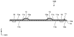
Backlight 7 comprise backboard 9(plate, covering, wall, member), parts 10(light-emitting device, illuminator, luminous circuit board, striation), 11(cover part, reflection horizon, covering, plate, reflecting plate), light guide member 12(light guide member body, diffusion layer, diffusion part), layers of prisms 7a, polarizing layer 7b and framework 7c.Each has backboard 9, reflection horizon 11, light guide member 12, layers of prisms 7a and polarizing layer 7b as the flat square configuration of watching from the front side (as an example, in this embodiment, rectangular shape), and piles up, to arrange shown in Fig. 3.
In this embodiment, parts 10 are arranged on respect on the relative side of light guide member 12 and display 4 (that is to say, as rear side or the back side of watching from the side of display 4).In this embodiment, as an example, a plurality of (as an example, in Fig. 3, four) parts 10 are positioned between backboard 9 and the reflection horizon 11.In the parts 10 each comprises circuit board 14(circuit board, printed wiring board, printed circuit board (PCB)), a plurality of illuminator 13(is referring to Fig. 5 to Fig. 7, light-emitting device, light source part, light source) and a plurality of (as an example, in Fig. 3, six) lens 10a(cover part, covering, light-operated product).Circuit board 14 is set to parallel with display 4, light guide member 12 etc.Each circuit board 14 comprises surperficial 14a and the side relative with surperficial 14a facing surfaces 14b(and display 4 on display 4 sides).Each circuit board 14 be configured to form (form of bar, elongated square configuration).Circuit board 14 is along the longitudinal direction setting of housing 2c.In addition, circuit board 14 is set on the short side direction of housing 2c spaced.Lens 10a is attached to surperficial 14a so that cover the state of light emission part 13 by bonding agent, welding, soldering etc.Reflected by each lens 10a from the light of each illuminator 13 emission, thereby enlarge light-struck scope (zone).In this embodiment, lens 10a is configured to different parts with illuminator 13.Yet, even also can obtain identical effect in lens 10a and the pattern that illuminator 13 is bonded to each other therein.
Circuit board 14(parts 10) the surperficial 14a layer 11 that is reflected covers.Reflection horizon 11 is configured to plate (film or plate), to have flexibility.Reflection horizon 11 comprises surperficial 11a and the side relative with surperficial 11a facing surfaces 11b(and display 4 on display 4 sides).A plurality of opening 11c(in this embodiment, as an example, through hole) be arranged at reflection horizon 11.Pass opening 11c from the light of illuminator 13 emissions towards light guide member 12.Opening 11c is set to respectively and lens 10a(illuminator 13) corresponding.In this embodiment, as an example, lens 10a is exposed to light guide member 12 by opening 11c, simultaneously reflection horizon 11 coating members 10.
Framework 7c is formed by the material with high relatively rigidity (for example, metal material etc.), and acts on backlight 7 and the housing of display unit 8 with backboard 9 usefulness.Backboard 9 comprises surperficial 9a and the side relative with surperficial 9a facing surfaces 9b(and display 4 on display 4 sides).
In addition, circuit board 15(second circuit board, circuit board, printed wiring board, printed circuit board (PCB)) on the side relative with display 4 (on surperficial 9b) be positioned on the backboard 9.As an example, circuit board 15 is attached to backboard 9 in the mode of the surperficial 9b certain intervals of distance backboard 9 by setting tool (for example, screw, not shown).At least the part of control circuit 17 (referring to Fig. 4) is by being installed in the structures such as parts on the circuit board 15.For example, control circuit 17 can comprise the screen signal processing circuit, tuner, HDMI (High Definition Multimedia Interface) (HDMI) signal processor, audio frequency and video (AV) entry terminal, the remote control signal receiver, controller (for example, CPU (central processing unit) (CPU 17a)), selector switch, display interface on the screen, memory module (for example, ROM (read-only memory) (ROM), random-access memory (ram), hard disk drive (HDD)), audio signal processing circuit, and signal supplying module 17b(does not illustrate the structure of not representing by Reference numeral).The output of the output (mobile image, rest image etc.) of control circuit 17 control by the video of the display screen 4A of display 4, the audio frequency by the loudspeaker (not shown), by being used for the ON/OFF of illuminator 13(element 18 backlight), the light that waits of other illuminator (for example, light emitting diode (LED)) launches.Display 4, loudspeaker, LED etc. are examples of output module.In addition, circuit board 15 can be coated with guard member 16.Guard member 16 to be forming such as the conductor of metal material, and covers the part of the circuit board 15 on the side relative with backboard 9 at least.
In addition, in this embodiment, as shown in Figure 4, as an example, each parts 10 comprises circuit board 14, illuminator 13, element 18 and connector 22.More specifically, for example, as an example, element 18(switch, on-off element, switch module, switch sections) be mos field effect transistor (MOS-FET).Illuminator 13 is for the light source that light is transmitted into display 4 (illuminating display 4) by light guide member 12.As an example, illuminator 13 is light emitting diode (LED).Connector 22(coupling part) is arranged at circuit board 14, and is electrically connected to corresponding connector 21(coupling part, and for example, be arranged at the connector of flexible print circuit (FPC)). Connector 21,22 comprises: be used for the terminal of supply capability, it is electrically connected to power supply 20; And the terminal that is used for signal (connection signal), it is electrically connected to signal supplying module 17b(connection signal supplying module).Signal supplying module 17b is the element (integrated circuit, packaging part) that is disposed on the circuit board 15.If according to will being applied to element 18 from signal supplying module 17b for the signal (in this case, grid voltage) of connecting element 18 from the instruction of CPU 17a, electric current and the source electrode of element 18 and drain electrode between flow, so connect element 18.Then, electric current (electric power) is supplied to illuminator 13 from power supply 20, so that illuminator 13 is luminous.Fig. 4 shows an example, and wherein, element 18 switches in the photoemissive beginning of two illuminators 13 and between stopping.Yet this embodiment is not limited thereto structure.For example, an element 18 can switch between the connecting and disconnecting of an illuminator 13, perhaps element 18 can equal or connecting and disconnecting more than three illuminators 13 between switch.
As shown in Figure 4, in this embodiment, control circuit 17 comprises CPU 17a, and signal supplying module 17b is arranged on the circuit board 15, this circuit board is positioned on the back side of backboard 9 (on the side relative with display 4) in housing 2c, and element 18 is arranged on the circuit board 14 that is different from circuit board 15.Traditionally, element 18 has been arranged on the circuit board 15, and any (for example, signal supplying module 17b) in the control circuit 17 is set on this circuit board.Because the quantity of element 18 and the quantity of illuminator 13 are proportional, and because element 18 is given birth to heat, so element 18 has been separated from each other to a certain extent.Therefore, the circuit board 15 at the back side of backboard 9 has been configured to big relatively, for setting element 18.On the other hand, for the circuit of the various functions that realize video display devices 1 and parts are contained in backboard 9 at housing 2c the back side.According to this embodiment, element 18 can reduce or removal from circuit board 15.Therefore, as an example, it is little that circuit board 15 is easy to the quantity that is configured to than element 18.Therefore, as an example, in housing 2c in the space at the back side of backboard 9, the degree of freedom of the layout of reinforcing member easily.In addition, as an example, in some cases, when the enough board area that is difficult in the space at the back side of backboard 9 in housing 2c to guarantee for the heat dissipation of element 18, may be difficult to guarantee the heat dissipation performance of element 18.It should be noted that as an example, in this embodiment, element 18 is arranged on the identical circuit board 14 with illuminator 13.Yet this embodiment is not limited thereto.When arrange among the housing 2c and its when being provided with the different circuit board of the circuit board 15 of control circuit 17, element 18 can be arranged on this circuit board.For example, this circuit board can be different from the circuit board 14,15 that is arranged between power supply 20 or signal supplying module 17b and the element 18, and this circuit board can be with signal and the distributing electric power circuit board to a plurality of circuit boards 14 etc.
As an example, in this embodiment, as shown in Figure 5, each circuit board 14 is configured to the square configuration (rectangular shape) of elongated plate-like (band shape).A plurality of (in this embodiment, as an example, six) illuminator 13 becomes a row ground to be arranged in center section (in this embodiment, as an example, middle body) along the longitudinal direction of circuit board 14 with constant spacing on the Width of circuit board 14 to locate.Each illuminator 13 is covered by lens 10a.Lens 10a presents the outward appearance that is roughly semisphere (dome shape), and in lens 10a the space (housing, space, chamber) that wherein accommodates illuminator 13 is set.In addition, as an example, in this embodiment, element 18 is arranged between the illuminator 13.Element 18 is positioned at center section (as an example, in this embodiment, middle body) at the Width of each circuit board 14 and locates.Therefore, in this embodiment, 18 one-tenth delegation ground of illuminator 13 and element are arranged.In the example of Fig. 5, an element 18 switches between the connecting and disconnecting of two illuminators 13.It should be noted that as an example, illuminator 13 and element 18 are surface mounted on the surperficial 14a of circuit board 14.
In addition, as shown in fig. 6 as an example in this embodiment, illuminator 13 and element 18 all are arranged on the surperficial 14a of circuit board 14.Therefore, as an example, conductive pattern (conductor part) can relatively easily be arranged on the circuit board 14.In addition, the surperficial 14a of circuit board 14, that is, the layer 11 that is reflected of the circuit board 14 on light guide member 12 sides (display 4 sides) covers.Lens 10a is from being arranged at opening 11c(second opening in reflection horizon 11) outstanding.Therefore, the light from illuminator 13 emissions can arrive light guide member 12.As an example, the surperficial 11a in reflection horizon 11 can be constructed so that reflected light easily at least.In this case, as an example, surperficial 11a has sleekly with color white.In addition, as another example, surperficial 11a can be constructed to be difficult to reflected light.In this case, as an example, surperficial 11a does not have sleekly with black colorant.As shown in Figure 6, the teat (projection) owing to element 18 is arranged on the surperficial 14a of circuit board 14.In this embodiment, as an example, reflection horizon 11 has flexibility.Therefore, reflection horizon 11 is according to the irregular slightly of circuit board 14 and can covering surfaces 14a in the deflection (bending).It should be noted that reflection horizon 11 can be configured to irregular shape in advance.Reflection horizon 11 can be fixed to circuit board 14, backlight 7 housing (for example, backboard 9) etc. by bonding agent or setting tool (for example, screw).
In this embodiment, as an example, as shown in Figure 6, illuminator 13, element 18 and connector 22(are referring to Fig. 5) be arranged at the surperficial 14a of circuit board 14, it is relative flat being configured to surperficial 14a facing surfaces 14b simultaneously.Therefore, in this embodiment, as an example, bonding agent that the surperficial 14b of circuit board 14 can be by having thermal conductivity etc. thermally is connected to the surperficial 9a of backboard 9.In this embodiment, as an example, surperficial 14b is adhering to each other on relative big zone with surperficial 9a.Therefore, according to this embodiment, as an example, be easy to strengthen the heat dissipation performance in the heat of illuminator 13 and element 18 generations.It should be noted that be inserted between circuit board 14 and the backboard 9 if will have thermal conductivity and flexibility or flexible member (for example, having the synthetic resin material of bubbling character), circuit board 14 can thermally be connected each other with backboard 9 so.In this case, even the surperficial 14b of circuit board 14 is irregular slightly, also be easy to heat is conducted to backboard 9 from circuit board 14.In addition, can use the adhesive tape (double sticky tape) with thermal conductivity to replace bonding agent 23.The thermal conductivity (conductivity) of expectation bonding agent 23 or adhesive tape is higher than the thermal conductivity (conductivity) of circuit board 14.
As mentioned above, in this embodiment, as an example, illuminator 13 and element 18 are arranged on the circuit board 14.Therefore, according to this embodiment, as an example, with element 18 control circuit 17(CPU 17a, signal supplying module 17b etc. of being provided with disposed thereon wherein) circuit board 15 on situation compare, circuit board 15 is easy to construct forr a short time.Therefore, be easy to the degree of freedom of the layout on the zone that reinforcing member is provided with circuit board 15 thereon.
In addition, in this embodiment, as an example, illuminator 13 and element 18 are arranged on the surperficial 14a of circuit board 14.Therefore, according to this embodiment, as an example, conductive pattern can be easily positioned on the surperficial 14a of circuit board 14() on.
In addition, in this embodiment, as an example, on circuit board 14, illuminator 13 is spaced from each other and in a row arranges, and element 18 is arranged between the illuminator 13.Therefore, according to this embodiment, as an example, circuit board 14 can easily be constructed forr a short time (thinner).In addition, as an example, conductive pattern can relatively easily form.
In addition, in this embodiment, as an example, the reflection horizon 11 that has flexibility and be used for covering board 14a is arranged between circuit board 14 and the light guide member 12, and opening 11c is arranged at reflection horizon 11, from the light of illuminator 13 towards light guide member 12 by this opening.Therefore, according to this embodiment, as an example, do not preventing that the light from illuminator 13 from arriving under the situation of light guide member 12, reflection horizon 11 can be arranged on the circuit board 14 in light guide member 12 sides along with the irregular of surperficial 14a of circuit board 14.Therefore, as an example, can easily suppress the inequality of the light (backlight) at display 4 places by the effect in reflection horizon 11, that is, and the variation of depending on the position of the brightness on the display screen 4a.
In addition, in this embodiment, as an example, the backboard 9 that thermally is connected to circuit board 14 is arranged on the circuit board 14 in the side relative with display 4.Therefore, according to this embodiment, as an example, can easily strengthen the heat dissipation performance in the heat of illuminator 13 and element 18 generations.
First modification is identical with above-mentioned first embodiment as shown in Figure 7, replaces 11 this point of reflection horizon except reflection horizon 11A is set.Therefore, also obtained same effect based on same configuration by first modification.Reflection horizon 11A in first modification can replace the reflection horizon 11 in above-mentioned first embodiment and use.Opening 11d(in this embodiment, as an example, through hole) be arranged at reflection horizon 11A, and element 18 exposes (giving prominence to) in light guide member 12 from opening 11d.That is to say that element 18 is by (passing) opening 11d.Therefore, according to first modification, as an example, reflection horizon 11A is made more flat.It should be noted, can be in the part that is exposed to light guide member 12 from opening 11d (for example, the part of the surperficial 14a of circuit board 14 and element 18) go up and (for example carry out surface treatment, be coated with white paint), the optical characteristics that approaches with these optical characteristics that have with the surface of reflection horizon 11A.
Identical with above-mentioned first embodiment with second modification shown in Fig. 9 as Fig. 8, except element 18 is arranged on the last this point of surperficial 14b of circuit board 14.Therefore, also obtained same effect according to same configuration by second modification.Parts 10B in second modification can replace the parts 10 in above-mentioned first embodiment and use.Element 18 is installed on the surperficial 14b of circuit board 14.According to second modification, element 18 is arranged on the surperficial 14b.Therefore, as an example, be easy to irregular by element 18 inhibitory reflex layers 11.In addition, as an example, be separated from each other because illuminator 13 is arranged as further with element 18, therefore be easy to strengthen the heat dissipation performance in the heat of illuminator 13 and element 18 generations.
Identical with above-mentioned first embodiment with the 3rd modification shown in Figure 11 as Figure 10, except opening 14c be arranged at circuit board 14C and at least the part of element 18C be arranged in the opening 14c this point.Therefore, also obtained same effect according to same configuration by the 3rd modification.Parts 10C in the 3rd modification can replace the parts 10 in above-mentioned first embodiment and use.With respect to surperficial 18a to the side (as in Figure 10 from above watch, outside from surperficial 18a) outstanding terminal 18b is arranged at the surperficial 18a of element 18C.Element 18C is arranged in the state of the opening 14c of circuit board 14C therein, and terminal 18b is projected on its marginal portion (surperficial 14a) from opening 14c.In addition, the segment conductor pattern on terminal 18b and the surperficial 14a mutually combines by soldering etc., makes to be electrically connected to each other.Therefore, according to the 3rd modification, as an example, reflection horizon 11 is made more flat.In addition, conductive pattern can more easily be arranged on the surperficial 14a of circuit board 14C() on.
The 5th modification is identical with above-mentioned first embodiment as shown in Figure 12, except element 18 is orientated the capable this point of the illuminator 13 that departs from the circuit board 14D as.Therefore, also obtained same effect according to same configuration by the 4th modification.According to the 4th modification, as an example, element 18 and illuminator 13 are orientated as further and are separated from each other.In addition, in the 4th modification, when on the direction that intersects with the row of illuminator 13 and when watching along the sight line of the surperficial 14a of circuit board 14D, element 18 is positioned between the illuminator 13.Therefore, as an example, can easily strengthen the heat dissipation performance in the heat of illuminator 13 and element 18 generations.Parts 10D in the 4th modification can replace the parts 10 in above-mentioned first embodiment and use.
The 5th modification is identical with above-mentioned first embodiment as shown in Figure 13, and row and the element 18 of orientating the illuminator 13 that departs from the circuit board 14E except element 18 as are capable of the crenellation pattern layout this point with respect to these.Therefore, also obtained same effect according to same configuration by the 5th modification.In the 5th modification, towards the direction that intersects with the row of illuminator 13 (for example, in Figure 13, upwards) depart from illuminator 13 row element 18 with towards the side of intersecting with row with illuminator 13 in the opposite direction (for example, in Figure 13, downwards) element 18 that departs from the row of illuminator 13 alternately arranges along every row.In addition, in the 5th modification, on the direction that intersects with the row of illuminator 13 and along the sight line of the surperficial 14a of circuit board 14E, element 18 is positioned between the illuminator 13.Therefore, according to the 5th modification, as an example, element 18 and illuminator 13 are orientated as further and are separated from each other, and element 18 is orientated as further and is separated from each other.Therefore, as an example, can easily strengthen the heat dissipation performance in the heat of illuminator 13 and element 18 generations.Parts 10E in the 5th modification can replace the parts 10 in above-mentioned first embodiment and use.
According to above-mentioned embodiment and modification, as an example, can obtain wherein more effectively video display devices and the light-emitting device of arrangement component.
Although described some embodiments, these embodiments only are that the mode by example presents, and are not used in the scope of the present invention that limits.In fact, herein the method and system of the novelty of Miao Shuing can embody with multiple other form; In addition, under the situation that does not depart from spirit of the present invention, can make various omissions, replacement and change to the form of the method and system described herein.Claims and equivalent thereof are intended to cover as dropping on these forms or the modification in the scope and spirit of the present invention.In addition, the specification of structure element (structure, type, direction, shape, size, length, width, thickness, highly, quantity, layout, position, material etc.) can suitably change, in order to carry out.For example, the shape of circuit board, size, quantity, illuminator and the element layout on circuit board etc. can suitably change, in order to carry out.For example, the multirow illuminator can be arranged on the circuit board, and a plurality of illuminator can be arranged to another shape (form, layout, pattern).The layout of element also can suitably change.For example, illuminator and element can be with matrix arrangement on circuit boards, and layout of illuminator and element, density etc. can be configured to change according to the position of photoconduction to module.In addition, in above-mentioned embodiment and modification, described light-emitting device wherein and be positioned at the so-called underneath type structure of photoconduction on the module in the side relative with display.Yet, according to light-emitting device of the present invention can be applied to light-emitting device (parts) wherein orientate as make when in the same manner from the top (front side) relative with the marginal portion of light bootstrap module along the marginal portion when watching display screen (towards) so-called lateral edges formula construct.
In addition, the various modules of the system of describing herein can be embodied as software application, hardware and/or software module or such as the parts on one or more computing machines of server.Although show a plurality of modules respectively, they can share identical basic logic or some or all in the code.
Claims (11)
1. video display devices, described video display devices comprises:
Housing;
The display that comprises screen, the part of described at least display are contained in the described housing;
Illuminator, described illuminator are configured to light is transmitted on the described display;
Element, described element are configured to switch supplying power to described illuminator and be not supplied between the described illuminator;
Controller, described controller is configured to control described element, with by the described electric power of described component feeding and do not supply with between the described electric power and switch; And
Circuit board, described circuit board comprise first surface and with described first surface opposing second surface, and be provided with described illuminator and described element.
2. video display devices according to claim 1 also comprises second circuit board, and the part of described at least controller is arranged at described second circuit board.
3. video display devices according to claim 1, wherein, described illuminator and described element are arranged on one in described first surface and the described second surface.
4. video display devices according to claim 3, wherein,
Described circuit board is provided with opening, and
Described element is arranged on the state in the described opening and arranges with the part of described at least element wherein.
5. video display devices according to claim 1, wherein, described illuminator is arranged on one in described first surface and the described second surface, and described element is arranged on another person in described first surface and the described second surface.
6. video display devices according to claim 1 wherein, be provided with a plurality of illuminators and spacedly, and described element is arranged between the described illuminator with becoming delegation on the described circuit board.
7. video display devices according to claim 1 wherein, be provided with a plurality of illuminators and spacedly, and described element is arranged on the position of the row that departs from described illuminator with becoming delegation on the described circuit board.
8. video display devices according to claim 7, wherein, when the sight line along the described first surface of described circuit board or described second surface on the direction that intersects with described row was watched, described element was positioned between the described illuminator.
9. video display devices according to claim 1 also comprises:
Flexible covering, described flexible covering is configured to cover described circuit board from a side of described display, wherein
Described covering is provided with second opening, from the light of described illuminator by the side transmission of described second opening towards described display.
10. video display devices according to claim 1 also comprises the wall that has thermal conductivity and thermally be connected to described circuit board, and described wall is arranged on the side relative with described display of described circuit board.
11. a light-emitting device, described light-emitting device comprises:
Illuminator, described illuminator are configured to light is transmitted on the display;
Element, described element are configured to switch supplying power to described illuminator and be not supplied between the described illuminator; And
Circuit board, described circuit board comprise first surface and with described first surface opposing second surface, and be provided with described illuminator and described element.
Applications Claiming Priority (2)
| Application Number | Priority Date | Filing Date | Title |
|---|---|---|---|
| JP2012044520A JP2013182076A (en) | 2012-02-29 | 2012-02-29 | Video display device and light emission device |
| JP2012-044520 | 2012-02-29 |
Publications (1)
| Publication Number | Publication Date |
|---|---|
| CN103295478A true CN103295478A (en) | 2013-09-11 |
Family
ID=49096257
Family Applications (1)
| Application Number | Title | Priority Date | Filing Date |
|---|---|---|---|
| CN2013100063839A Pending CN103295478A (en) | 2012-02-29 | 2013-01-08 | Video display device and illuminating device |
Country Status (2)
| Country | Link |
|---|---|
| JP (1) | JP2013182076A (en) |
| CN (1) | CN103295478A (en) |
Families Citing this family (10)
| Publication number | Priority date | Publication date | Assignee | Title |
|---|---|---|---|---|
| WO2017038084A1 (en) | 2015-09-01 | 2017-03-09 | パナソニックIpマネジメント株式会社 | Video display device |
| EP3346323B1 (en) | 2015-09-01 | 2020-03-04 | Panasonic Intellectual Property Management Co., Ltd. | Image display device |
| US10809569B2 (en) | 2015-09-01 | 2020-10-20 | Panasonic Intellectual Property Management Co., Ltd. | Video display device |
| US10643556B2 (en) | 2015-09-01 | 2020-05-05 | Panasonic Intellectual Property Management Co., Ltd. | Video display device |
| US10490143B2 (en) | 2015-09-01 | 2019-11-26 | Panasonic Intellectual Property Management Co., Ltd. | Video display device |
| WO2017038085A1 (en) * | 2015-09-01 | 2017-03-09 | パナソニックIpマネジメント株式会社 | Image display device |
| WO2017137653A1 (en) * | 2016-02-09 | 2017-08-17 | Nanocomp Oy Ltd | Light guide with plurality of light channels |
| US11428987B2 (en) | 2020-05-22 | 2022-08-30 | Apple Inc. | Electronic device display with a backlight having light-emitting diodes and driver integrated circuits in an active area |
| EP3933495A1 (en) * | 2020-07-03 | 2022-01-05 | InnoLux Corporation | Backlight module and display device |
| CN113888956A (en) * | 2020-07-03 | 2022-01-04 | 群创光电股份有限公司 | Backlight module and display device |
Citations (9)
| Publication number | Priority date | Publication date | Assignee | Title |
|---|---|---|---|---|
| CN1693966A (en) * | 2005-06-15 | 2005-11-09 | 友达光电股份有限公司 | Backlight module structure |
| CN2760603Y (en) * | 2004-11-26 | 2006-02-22 | 比亚迪股份有限公司 | Part flush type ultra-thin liquid crystal display module |
| CN1766711A (en) * | 2004-10-30 | 2006-05-03 | Lg.菲利浦Lcd株式会社 | Light emitting diode backlight unit and liquid crystal display device using the same |
| CN1956045A (en) * | 2005-10-29 | 2007-05-02 | Lg.菲利浦Lcd株式会社 | Backlight unit and driving method using the same |
| CN1984533A (en) * | 2005-12-13 | 2007-06-20 | 三星电机株式会社 | Printed circuit board having embedded electronic components and manufacturing method thereof |
| CN101008742A (en) * | 2006-01-26 | 2007-08-01 | 启萌科技有限公司 | Back lighting module of liquid crystal display device |
| CN102077266A (en) * | 2008-07-11 | 2011-05-25 | 夏普株式会社 | Backlight drive device, display device using the same, and backlight drive method |
| CN102235624A (en) * | 2010-05-04 | 2011-11-09 | Lg伊诺特有限公司 | Backlight unit and display device |
| CN102300418A (en) * | 2011-08-12 | 2011-12-28 | 东莞康源电子有限公司 | Embedded component type PCB manufacturing method |
-
2012
- 2012-02-29 JP JP2012044520A patent/JP2013182076A/en active Pending
-
2013
- 2013-01-08 CN CN2013100063839A patent/CN103295478A/en active Pending
Patent Citations (9)
| Publication number | Priority date | Publication date | Assignee | Title |
|---|---|---|---|---|
| CN1766711A (en) * | 2004-10-30 | 2006-05-03 | Lg.菲利浦Lcd株式会社 | Light emitting diode backlight unit and liquid crystal display device using the same |
| CN2760603Y (en) * | 2004-11-26 | 2006-02-22 | 比亚迪股份有限公司 | Part flush type ultra-thin liquid crystal display module |
| CN1693966A (en) * | 2005-06-15 | 2005-11-09 | 友达光电股份有限公司 | Backlight module structure |
| CN1956045A (en) * | 2005-10-29 | 2007-05-02 | Lg.菲利浦Lcd株式会社 | Backlight unit and driving method using the same |
| CN1984533A (en) * | 2005-12-13 | 2007-06-20 | 三星电机株式会社 | Printed circuit board having embedded electronic components and manufacturing method thereof |
| CN101008742A (en) * | 2006-01-26 | 2007-08-01 | 启萌科技有限公司 | Back lighting module of liquid crystal display device |
| CN102077266A (en) * | 2008-07-11 | 2011-05-25 | 夏普株式会社 | Backlight drive device, display device using the same, and backlight drive method |
| CN102235624A (en) * | 2010-05-04 | 2011-11-09 | Lg伊诺特有限公司 | Backlight unit and display device |
| CN102300418A (en) * | 2011-08-12 | 2011-12-28 | 东莞康源电子有限公司 | Embedded component type PCB manufacturing method |
Also Published As
| Publication number | Publication date |
|---|---|
| JP2013182076A (en) | 2013-09-12 |
Similar Documents
| Publication | Publication Date | Title |
|---|---|---|
| CN103295478A (en) | Video display device and illuminating device | |
| US7593087B2 (en) | Liquid crystal display device and portable display apparatus using the same | |
| US20110205145A1 (en) | Optoelectronic Device, Display and Backlight Module | |
| US20080094321A1 (en) | Organic light emitting diode display and method of manufacture | |
| US11378850B2 (en) | Substrate assembly, display panel and display device | |
| KR20200063125A (en) | Backlight apparatus | |
| US11391885B2 (en) | Light bar assembly, backlight unit, display unit and mobile electronic device | |
| CN101086827A (en) | Driving device and a liquid crystal display including the same | |
| US20240019736A1 (en) | Display apparatus and light source device thereof | |
| CN107710062B (en) | Structure for connecting printed circuit boards and display device having the same | |
| US11262620B1 (en) | Display apparatus and light source device thereof | |
| KR20220098660A (en) | Display apparatus and light apparatus thereof | |
| KR20220081577A (en) | Display apparatus and light apparatus thereof | |
| KR101321230B1 (en) | Liquid crystal display device | |
| US11205642B2 (en) | Twistable light emitting diode display module | |
| US20240027832A1 (en) | Display apparatus | |
| US11934064B2 (en) | Display apparatus and light source apparatus thereof | |
| US20230075434A1 (en) | Light emitting diode module and display apparatus having the same | |
| US20230251525A1 (en) | Connector, printed circuit board mounting the connector, and display apparatus including the same | |
| US20230307587A1 (en) | Display apparatus | |
| EP4050408A1 (en) | Display device and light source device thereof | |
| US20220260877A1 (en) | Display apparatus and light source device thereof | |
| CN117897654A (en) | Connector, printed circuit board mounted with connector, and display device having connector | |
| KR20240011576A (en) | Display apparatus | |
| KR20230140317A (en) | Display apparatus and light apparatus thereof |
Legal Events
| Date | Code | Title | Description |
|---|---|---|---|
| C06 | Publication | ||
| PB01 | Publication | ||
| C10 | Entry into substantive examination | ||
| SE01 | Entry into force of request for substantive examination | ||
| C02 | Deemed withdrawal of patent application after publication (patent law 2001) | ||
| WD01 | Invention patent application deemed withdrawn after publication |
Application publication date: 20130911 |