CN102754230A - Thermoelectric generation module - Google Patents
Thermoelectric generation module Download PDFInfo
- Publication number
- CN102754230A CN102754230A CN2011800096210A CN201180009621A CN102754230A CN 102754230 A CN102754230 A CN 102754230A CN 2011800096210 A CN2011800096210 A CN 2011800096210A CN 201180009621 A CN201180009621 A CN 201180009621A CN 102754230 A CN102754230 A CN 102754230A
- Authority
- CN
- China
- Prior art keywords
- diffusion preventing
- preventing layer
- thermoelectric generation
- layer
- nickel
- Prior art date
- Legal status (The legal status is an assumption and is not a legal conclusion. Google has not performed a legal analysis and makes no representation as to the accuracy of the status listed.)
- Granted
Links
Images


Classifications
-
- H—ELECTRICITY
- H10—SEMICONDUCTOR DEVICES; ELECTRIC SOLID-STATE DEVICES NOT OTHERWISE PROVIDED FOR
- H10N—ELECTRIC SOLID-STATE DEVICES NOT OTHERWISE PROVIDED FOR
- H10N10/00—Thermoelectric devices comprising a junction of dissimilar materials, i.e. devices exhibiting Seebeck or Peltier effects
- H10N10/80—Constructional details
- H10N10/81—Structural details of the junction
- H10N10/817—Structural details of the junction the junction being non-separable, e.g. being cemented, sintered or soldered
-
- H—ELECTRICITY
- H10—SEMICONDUCTOR DEVICES; ELECTRIC SOLID-STATE DEVICES NOT OTHERWISE PROVIDED FOR
- H10N—ELECTRIC SOLID-STATE DEVICES NOT OTHERWISE PROVIDED FOR
- H10N10/00—Thermoelectric devices comprising a junction of dissimilar materials, i.e. devices exhibiting Seebeck or Peltier effects
- H10N10/10—Thermoelectric devices comprising a junction of dissimilar materials, i.e. devices exhibiting Seebeck or Peltier effects operating with only the Peltier or Seebeck effects
-
- H—ELECTRICITY
- H10—SEMICONDUCTOR DEVICES; ELECTRIC SOLID-STATE DEVICES NOT OTHERWISE PROVIDED FOR
- H10N—ELECTRIC SOLID-STATE DEVICES NOT OTHERWISE PROVIDED FOR
- H10N10/00—Thermoelectric devices comprising a junction of dissimilar materials, i.e. devices exhibiting Seebeck or Peltier effects
-
- H—ELECTRICITY
- H10—SEMICONDUCTOR DEVICES; ELECTRIC SOLID-STATE DEVICES NOT OTHERWISE PROVIDED FOR
- H10N—ELECTRIC SOLID-STATE DEVICES NOT OTHERWISE PROVIDED FOR
- H10N10/00—Thermoelectric devices comprising a junction of dissimilar materials, i.e. devices exhibiting Seebeck or Peltier effects
- H10N10/10—Thermoelectric devices comprising a junction of dissimilar materials, i.e. devices exhibiting Seebeck or Peltier effects operating with only the Peltier or Seebeck effects
- H10N10/17—Thermoelectric devices comprising a junction of dissimilar materials, i.e. devices exhibiting Seebeck or Peltier effects operating with only the Peltier or Seebeck effects characterised by the structure or configuration of the cell or thermocouple forming the device
Abstract
Disclosed is a thermoelectric generation module which can withstand prolonged use in high-temperature environments such as those where the temperature (Th) of the high temperature section exceeds 250 DEG C. The disclosed thermoelectric generation module includes: a thermoelectric generation element (20); first diffusion barrier layers (71) which are disposed on the surface of the thermoelectric generation element (20) and which comprise molybdenum (Mo); second diffusion barrier layers (73) which are disposed on the surface on the opposite side of the first diffusion barrier layers (71) to the thermoelectric generation element (20) and which comprise a nickel-tin (Ni-Sn) intermetallic compound; electrodes (40); ; third diffusion barrier layers (42) which are disposed on the surface of the electrodes (40) and which comprise a nickel-tin (Ni-Sn) intermetallic compound, and solder layers (80) which connect the second diffusion barrier layers (73) and the third diffusion barrier layers (42) and which contain at least 85% lead (Pb).
Description
Technical field
The present invention relates to a kind of thermoelectric generation module through adopting thermoelectric generation elements to utilize temperature difference to generate electricity.
Background technology
All the time, the known thermoelectric power generation that has thermoelectric generation elements to be configured in and to generate electricity between high temperature side heat exchanger and the low-temperature side heat exchanger.Thermoelectric generation elements is to have used the member of the thermoelectric effect that is called as " Seebeck effect ".Adopting under the situation of semi-conducting material as thermoelectric material, constituting thermoelectric generation module through the thermoelectric generation elements that will form with by the thermoelectric generation elements combination that the thermoelectric material of N type forms by the thermoelectric material of P type.The not only simple in structure and processing ease of such thermoelectric generation module; Can also keep stable properties; Therefore, the application for the thermoelectric power generation of generating electricity to the heat that utilizes from the gas of the discharges such as stove of the engine of motor vehicle or factory conducts a research widely.
But, thermoelectric generation module is in order to obtain high conversion efficiency of thermoelectric, increase under such temperature environment in the difference of the temperature that makes high-temperature portion as much as possible (Th) and the temperature (Tc) of low-temp. portion to use.For example, adopted under will be in the temperature (Th) of the high-temperature portion the highest temperature environment that becomes 280 ℃ of that kind of the thermoelectric generation module of the thermoelectric material that representative bismuth-tellurium (Bi-Te) is and used.
The purposes of existing electrothermal module is mainly used in cooling, as the scolder that is used for electrode is connected in thermoelectric element, employing be the lead-free solder etc. of scolder or Sn-Ag-Cu etc. of the eutectic system of 37%Pb-63%Sn.In addition, in thermoelectric element, spread in order to prevent scolder, employing be the interphase (with reference to the open JP-A-10-135523 of Japan's patent application) of nickel (Ni) or nickel-Xi (Ni-Sn).As electrode, generally adopt copper (Cu), good for the wettability that makes scolder, adopt method such as plating mostly and on electrode, form the nickel film.
In JP-A-10-135523, pointed out as preventing that scolder from using in the thermoelectric device of nickel to the diffusion preventing layer of thermoelectric element diffusion, be that the thin diffusion preventing layer of a few μ m can't stop diffusion reliably through thickness.On the other hand, pointed out under the situation of the thick diffusion preventing layer that has adopted nickel that the thick-layer of nickel is along the boundary layer of block and stop diffusion powerfully, but the contact strength generation deterioration of the thick-layer of nickel and thermoelectric element.
To this; In order to improve the effect of diffusion preventing further; Improve the diffusion preventing layer structure intensity and make the reliability growth of thermoelectric device, the diffusion preventing layer structure that in patent documentation 1, discloses the thermoelectric device of the fish plate that conductor element with N type and P type and conductor element with N type and P type be connected with circuit is made at least 1 layer of thickness 50~3000 μ m by interphase Ni-Sn.And then the structure that discloses the diffusion preventing layer is made as the metal level that is made up of the layer of interphase Ni-Sn and the articulamentum that contains tin.
On the other hand; Under with the situation of generating as purpose; In order at high temperature to use electrothermal module,, proposed to adopt the scolder (with reference to the open JP-P2009-231317A of Japan's patent application) that contains the lead (Pb) more than 85% as the scolder that is used for electrode is connected with thermoelectric element.
In JP-P2009-231317A, the height (short transverse of thermoelectric element) that discloses electrothermal module keeps constant and can guarantee sufficient joint strength, can prevent the outstanding electrothermal module that destroys that produces owing to scolder in addition.This electrothermal module is for by P type thermoelectric element, N type thermoelectric element, electrode member and electrothermal module that the scolder of these member engages is constituted, and scolder is made up of scolder base material and particle (copper ball).And then, in JP-P2009-231317A, disclose the scolder base material and contained the lead more than 85%.Containing ratio through with the lead of scolder is made as more than 85%, even if for example under 260 ℃ high temperature, scolder also can not fuse but keep engaging, thereby can electrode member be engaged with thermoelectric element well.
In addition, as the nonproliferation film of thermoelectric element, (with reference to the open JP-P2008-10612A of Japan's patent application) such as employing molybdenum (Mo) films proposed.As the solder bonds layer, what adopt is the nickel film all the time.
In JP-P2008-10612A, disclose with respect to contain the thermoelectric element of the high diffusion preventing layer of diffusion preventing effect height that at least a thermoelectric material in bismuth, tellurium, selenium, the antimony can forming element and peel strength.This thermoelectric element has: contain the two or more thermoelectric material in bismuth (Bi), tellurium (Te), selenium (Se), the antimony (Sb); Be formed on the thermoelectric material, and prevent the diffusion preventing layer of xenogenesis element with respect to the diffusion of thermoelectric material; Be formed on the diffusion preventing layer, and with the solder bonds layer of diffusion preventing layer and solder bonds, the peel strength in the interface of the interface of thermoelectric material layer and diffusion preventing layer or diffusion preventing layer and solder bonds layer is more than the 0.6MPa.And then, in JP-P2008-10612A, disclose the diffusion preventing layer contain molybdenum (Mo), tungsten (W), niobium (Nb), and tantalum (Ta) in any.
But; Under the environment of temperature above the high temperature of 250 ℃ of that kind of high-temperature portion; Adopting under the situation of nickel as prevent the diffusion preventing layer that scolder spreads in thermoelectric element; Nickel diffusion and segregation and the resistance value of joint interface is risen in solder layer on the contrary, perhaps the copper of electrode spread in thermoelectric element via solder layer and the resistance value of thermoelectric element is risen, and has produced the such problem of output power reduction of electrothermal module under 1000~2000 hours long-time use thus.
Summary of the invention
[problem that invention will solve]
To this, the present invention makes in view of the above-mentioned problems, and its purpose is, a kind of thermoelectric generation module that under the environment of temperature above the high temperature of 250 ℃ of that kind of high-temperature portion, can use for a long time is provided.
[being used to solve the means of problem]
To achieve these goals, a related thermoelectric generation module of viewpoint of the present invention comprises: thermoelectric generation elements; Be configured in the surface of thermoelectric generation elements, and the first diffusion preventing layer that constitutes by molybdenum (Mo); Be configured in the first diffusion preventing layer and face thermoelectric generation elements side opposition side, and the second diffusion preventing layer that constitutes by the interphase of nickel-Xi (Ni-Sn); Electrode; Be configured in the surface of electrode, and the 3rd diffusion preventing layer that constitutes by the interphase of nickel-Xi (Ni-Sn); The second diffusion preventing layer is engaged with the 3rd diffusion preventing layer, and contain the solder layer of lead (Pb) more than 85%.
[invention effect]
As preventing that scolder from using under the situation of molybdenum to the diffusion preventing layer of thermoelectric generation elements diffusion, because molybdenum do not engage with scolder well, so through carrying out good engaging disposing nickel dam between the diffusion preventing layer of molybdenum and the solder layer.But, produced under the environment of high temperature nickel to the such problem of scolder diffusion.According to a viewpoint of the present invention; Through nickel being changed to the interphase of nickel-Xi; Can suppress the diffusion of nickel in solder layer, thereby a kind of thermoelectric generation module that under the environment of temperature above the high temperature of 250 ℃ of that kind of high-temperature portion, can use for a long time can be provided.
Description of drawings
Fig. 1 is the stereogram of the summary of the related thermoelectric generation module of expression each execution mode of the present invention.
Fig. 2 is that the part of thermoelectric generation module that comparative example is related is amplified the cutaway view of expression.(a) of Fig. 2 shows the initial condition of thermoelectric generation module, and (b) of Fig. 2 schematically shows the state of the thermoelectric generation module after long-time placement the under the environment of high temperature.
Fig. 3 is that the part of thermoelectric generation module that first execution mode of the present invention is related is amplified the cutaway view of expression.
Fig. 4 is that the part of thermoelectric generation module that the variation of first execution mode of the present invention is related is amplified the cutaway view of expression.
Fig. 5 is that the part of thermoelectric generation module that second execution mode of the present invention is related is amplified the cutaway view of expression.
Fig. 6 is that the part of thermoelectric generation module that the variation of second execution mode of the present invention is related is amplified the cutaway view of expression.
Fig. 7 is used for figure that the method for life of predicting thermoelectric generation module through Arrhenius model is described.
Fig. 8 is the figure that the activation energy that needs to the scolder diffusion with the activation energy that needs to the scolder diffusion for the nickel that makes monomer with for the nickel of the interphase that makes formation nickel-Xi compares expression.
Fig. 9 is that the part of thermoelectric generation module that comparative example is related is amplified the cutaway view of expression.(a) of Fig. 9 shows the initial condition of thermoelectric generation module, and (b) of Fig. 9 is schematically illustrated in the state of the thermoelectric generation module after down long-time placement of environment of high temperature.
Figure 10 is the cutaway view of the structure of thermoelectric generation elements that P type and N type are arranged of engaging respectively in the related thermoelectric generation module of expression first execution mode of the present invention and electrode.
Figure 11 is the cutaway view of the structure of thermoelectric generation elements that P type and N type are arranged of engaging respectively in the related thermoelectric generation module of expression second execution mode of the present invention and electrode.
Figure 12 is the cutaway view of experimental sample A of the structure of an expression part of having simulated the related thermoelectric generation module of comparative example.(a) of Figure 12 shows the initial condition of experimental sample A, and (b) of Figure 12 schematically shows the state of the experimental sample A after long-time placement the under the environment of high temperature.
Figure 13 is the microphotograph of the experimental sample A after long-time placement the under the environment of high temperature.
Figure 14 is the cutaway view of experimental sample B of the structure of an expression part of having simulated the related thermoelectric generation module of second execution mode of the present invention.(a) of Figure 14 shows the initial condition of experimental sample B, and (b) of Figure 14 schematically shows the state of the experimental sample B after long-time placement the under the environment of high temperature.
Figure 15 is the microphotograph of the experimental sample B after long-time placement the under the environment of high temperature.
Figure 16 is used for the figure that the variation to the output power of the related thermoelectric generation module of the related thermoelectric generation module of second execution mode of the present invention and comparative example compares.
Embodiment
Below, for execution mode of the present invention, on one side with reference to accompanying drawing explanation at length on one side.Need to prove, be marked with identical reference number, and omit explanation for identical structural element.
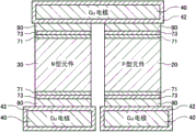
Fig. 1 is the stereogram of the summary of the related thermoelectric generation module of expression each execution mode of the present invention.In thermoelectric generation module 1; Through the thermoelectric generation elements (N type element) 30 that for example on the substrate that is formed by electrical insulating materials such as potteries (heat exchange substrate) 10, engages thermoelectric generation elements (P type element) 20 that the thermoelectric material by the P type forms and formed by the thermoelectric material of N type via electrode 40, it is right to form the PN element thus.And then, this PN element on the substrate (heat exchange substrate) 50 that forms by electrical insulating material of configuration.Need to prove, also can omit substrate 10 and/or substrate 50, and electrode 40 is directly joined with the surface with heat exchanger of electrical insulating property.
In this execution mode, P type element 20 and N type element 30 form by the thermoelectric material more than 2 kinds that contains in bismuth (Bi), tellurium (Te), selenium (Se), the antimony (Sb).Especially, under the temperature of high-temperature portion is the highest 280 ℃ temperature environment, the thermoelectric material that is suitable for bismuth-tellurium (Bi-Te) and is.
On the N type element of the P type element of the right end of the PN element that forms by a plurality of P type elements 20 and a plurality of N type element 30 and the other end, be electrically connected with lead-in wire 60 via electrode.When substrate 50 sides being applied heat, in thermoelectric generation module, produce electromotive force when substrate 10 sides being cooled off by cooling water etc., when on lead-in wire 60, connecting load (not shown), streaming current as shown in Figure 1.That is,, thereby can electric power be taken out through poor to the both sides of thermoelectric generation module 1 (among the figure about) additional temp.
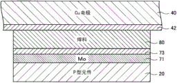
Fig. 2 is that the part of thermoelectric generation module that comparative example is related is amplified the cutaway view of expression.In Fig. 2,, show P type element 20 as the example of thermoelectric generation elements.In addition, (a) of Fig. 2 shows the initial condition of thermoelectric generation module, and (b) of Fig. 2 schematically shows the state of the thermoelectric generation module after long-time placement the under the environment of high temperature.
Shown in Fig. 2 (a); In this thermoelectric generation module; Interarea (upper surface among the figure) in thermoelectric generation elements (P type element) 20 is formed with diffusion preventing layer 71 by molybdenum (Mo), is formed with diffusion preventing layer 72 with face thermoelectric generation elements side opposition side by nickel (Ni) diffusion preventing layer 71.On the other hand, the interarea (lower surface among the figure) at the electrode 40 that is formed by copper (Cu) is formed with diffusion preventing layer 41 by nickel (Ni).And then, diffusion preventing layer 72 and diffusion preventing layer 41 through contain lead (Pb) more than 85% solder layer 80 and engage opposed to each other.
Like this, through forming molybdenum, prevented that the composition of nickel (Ni) from spreading to thermoelectric generation elements as diffusion preventing layer 71.On the other hand, through adopt nickel (Ni) as diffusion preventing layer 72, prevented that the scolder of solder layer 80 from spreading in thermoelectric generation elements.In addition, when the copper of electrode 40 spread in solder layer 80, copper might and then spread in thermoelectric generation elements, and the resistance value of thermoelectric generation elements is risen, and the output power of thermoelectric generation module is reduced.To this,, prevented the situation that the copper of electrode 40 spreads in solder layer 80 or thermoelectric generation elements through adopt nickel (Ni) as diffusion preventing layer 41.Simultaneously, through on diffusion preventing layer 71 and electrode 40, disposing nickel (Ni), thereby can improve the wettability of scolder.
But when under the related environment of thermoelectric generation module at high temperature of comparative example during long-time the placement, shown in Fig. 2 (b), the nickel that forms diffusion preventing layer 72 and 41 spreads in solder layer 80, as nickel (Ni) or nickel oxide (Ni-O) and segregation.Like this, nickel combines with oxygen and constitutes nickel oxide and break away from from diffusion preventing layer 72 and 41, and in this scolder diffusion, thereby the nickel that forms diffusion preventing layer 72 and 41 continues to reduce.
Consequently, a diffusion preventing layer 72 and a part of 41 or all disappear, be present in interface between diffusion preventing layer 72 and the diffusion preventing layer 71 based on the Ni-Mo alloy combine be cut off.In the zone that diffusion preventing layer 72 disappears, the interface between solder layer 80 and the diffusion preventing layer 71 (Pb/Mo interface) occurs, but because plumbous (Pb) do not form alloy with molybdenum (Mo), so interface resistance increases.Because the increase of such resistance value, the output power that has produced thermoelectric generation module reduces such problem.
Fig. 3 is that the part of thermoelectric generation module that first execution mode of the present invention is related is amplified the cutaway view of expression.In Fig. 3,, show P type element 20 as the example of thermoelectric generation elements.As shown in Figure 3; In this thermoelectric generation module; Interarea (upper surface among the figure) in thermoelectric generation elements (P type element) 20 is formed with diffusion preventing layer 71 by molybdenum (Mo), is formed with diffusion preventing layer 73 at diffusion preventing layer 71 and face thermoelectric generation elements side opposition side by the interphase of nickel-Xi (Ni-Sn).
On the other hand, be formed with diffusion preventing layer 42 at the interarea (lower surface among the figure) of the electrode 40 that forms by copper (Cu) by the interphase of nickel-Xi (Ni-Sn).And then, diffusion preventing layer 73 and diffusion preventing layer 42 through contain lead (Pb) more than 85% solder layer 80 and engage opposed to each other.
Thus; The diffusion preventing layer 71 that configuration is made up of molybdenum on P type element 20; The diffusion preventing layer 73 that configuration is made up of the interphase of nickel-Xi on diffusion preventing layer 71; Configuration solder layer 80 on diffusion preventing layer 73, the diffusion preventing layer 42 that configuration is made up of the interphase of nickel-Xi on solder layer 80, configured electrodes 40 on diffusion preventing layer 42.The thickness of each the diffusion preventing layer in this execution mode is 0.1 μ m~20 μ m.
Preferably, the containing ratio of the lead in the solder layer 80 is more than 90%, and in this case, the fusing point of scolder is more than 275 ℃.More preferably, the containing ratio of the lead in the solder layer 80 is more than 95%, and in this case, the fusing point of scolder is more than 305 ℃.And then if the containing ratio of the lead in the solder layer 80 is made as more than 98%, then the fusing point of scolder is more than 317 ℃.
According to this execution mode, change to the interphase of nickel-Xi through the nickel on the diffusion preventing layer 71 that will be configured in molybdenum, even if thermoelectric generation module long-time placement under the environment of high temperature also can be suppressed the diffusion of nickel in solder layer 80.Its reason is; Such as after the detailed description; The interphase that forms the nickel-Xi (Ni-Sn) of diffusion preventing layer 73 and 42 needs energy when being decomposed into nickel (Ni) and tin (Sn); So for the nickel that constitutes this interphase is spread in scolder, with the nickel of monomer in scolder, spread compare need be bigger energy.Through suppressing the diffusion of nickel to solder layer 80; Solder layer 80 does not occur with the interface (Pb/Mo interface) of diffusion preventing layer 71; Therefore suppress the increase of interface resistance, thereby produce reduction hardly because of the output power of the caused thermoelectric generation module of increase of resistance value.Thereby, a kind of thermoelectric generation module that under the environment of temperature above the high temperature of 250 ℃ of that kind of high-temperature portion, can use for a long time can be provided.
Fig. 4 is that the part of thermoelectric generation module that the variation of first execution mode of the present invention is related is amplified the cutaway view of expression.As shown in Figure 4; In this thermoelectric generation module; Interarea (upper surface among the figure) in thermoelectric generation elements (P type element) 20 is formed with diffusion preventing layer 71 by molybdenum (Mo); Be formed with diffusion preventing layer 73 at diffusion preventing layer 71 and face thermoelectric generation elements side opposition side by the interphase of nickel-Xi (Ni-Sn), be formed with solder bonds layer 74 with faces diffusion preventing layer 71 side opposition side by tin (Sn) diffusion preventing layer 73.
On the other hand, be formed with diffusion preventing layer 42 by the interphase of nickel-Xi (Ni-Sn), be formed with solder bonds layer 43 with the face electrode side opposition side by tin (Sn) diffusion preventing layer 42 at the interarea (lower surface among the figure) of the electrode 40 that forms by copper (Cu).And then, solder bonds layer 74 and solder bonds layer 43 through contain lead (Pb) more than 85% solder layer 80 and engage opposed to each other.
Thus; The diffusion preventing layer 71 that configuration is made up of molybdenum on P type element 20; The diffusion preventing layer 73 that configuration is made up of the interphase of nickel-Xi on diffusion preventing layer 71; The solder bonds layer 74 that configuration is made up of tin on diffusion preventing layer 73, configuration solder layer 80 on solder bonds layer 74, the solder bonds layer 43 that configuration is made up of tin on solder layer 80; On solder bonds layer 43, be formed with the diffusion preventing layer 42 that the interphase by nickel-Xi constitutes, configured electrodes 40 on diffusion preventing layer 42.The thickness of each the diffusion preventing layer in this variation and the thickness of each solder bonds layer are 0.1 μ m~20 μ m.
Like this, through forming solder bonds layer 74 and 43 respectively by tin on the diffusion preventing layer 73 and 42 that forms at the interphase by nickel-Xi (Ni-Sn), therefore the fusing point of tin can improve the wettability of scolder near the fusing point of scolder thus.In the variation of first execution mode; Through suppressing the diffusion of nickel to solder layer 80; Solder layer 80 does not occur with the interface (Pb/Mo interface) of diffusion preventing layer 71; Therefore, also can suppress the increase of interface resistance, thereby produce reduction hardly because of the output power of the caused thermoelectric generation module of increase of resistance value.
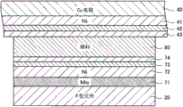
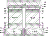
Fig. 5 is that the part of thermoelectric generation module that second execution mode of the present invention is related is amplified the cutaway view of expression.In Fig. 5,, show P type element 20 as the example of thermoelectric generation elements.As shown in Figure 5; In this thermoelectric generation module; Interarea (upper surface among the figure) in thermoelectric generation elements (P type element) 20 is formed with diffusion preventing layer 71 by molybdenum (Mo); Be formed with diffusion preventing layer 72 with face thermoelectric generation elements side opposition side by nickel (Ni) diffusion preventing layer 71, and then, be formed with diffusion preventing layer 73 at diffusion preventing layer 72 and faces diffusion preventing layer 71 side opposition side by the interphase of nickel-Xi (Ni-Sn).
On the other hand, be formed with diffusion preventing layer 41 by nickel (Ni), be formed with diffusion preventing layer 42 by the interphase of nickel-Xi (Ni-Sn) at diffusion preventing layer 41 and the face electrode side opposition side at the interarea (lower surface among the figure) of the electrode 40 that forms by copper (Cu).And then, diffusion preventing layer 73 and diffusion preventing layer 42 through contain lead (Pb) more than 85% solder layer 80 and engage opposed to each other.
Thus; The diffusion preventing layer 71 that configuration is made up of molybdenum on P type element 20; The diffusion preventing layer 72 that configuration is made up of nickel on diffusion preventing layer 71; The diffusion preventing layer 73 that configuration is made up of the interphase of nickel-Xi on diffusion preventing layer 72, configuration solder layer 80 on diffusion preventing layer 73, the diffusion preventing layer 42 that configuration is made up of the interphase of nickel-Xi on solder layer 80; The diffusion preventing layer 41 that configuration is made up of nickel on diffusion preventing layer 42, configured electrodes 40 on diffusion preventing layer 41.The thickness of each the diffusion preventing layer in this execution mode is 0.1 μ m~20 μ m.
Preferably, the containing ratio of the lead in the solder layer 80 is more than 90%, and in this case, the fusing point of scolder is more than 275 ℃.More preferably, the containing ratio of the lead in the solder layer 80 is more than 95%, and in this case, the fusing point of scolder is more than 305 ℃.And then if the containing ratio of the lead in the solder layer 80 is made as more than 98%, then the fusing point of scolder is more than 317 ℃.
Thermoelectric generation elements causes distortion under the environment of high temperature, thereby causes in the junction surface the thermoelectric generation elements stress application.In addition, the diffusion preventing layer 71 of molybdenum is thinner than thermoelectric generating element, therefore, under the environment of high temperature, follows the distortion of thermoelectric generation elements and likewise causes distortion, thereby cause diffusion preventing layer 71 stress application.According to this execution mode,, thereby can relax the stress that imposes on thermoelectric generation elements and diffusion preventing layer 71 through the diffusion preventing layer 72 of configuration nickel between the diffusion preventing layer 73 of the diffusion preventing layer 71 of molybdenum and nickel-Xi.
In addition, because the diffusion preventing layer 73 of nickel-Xi and 41 existence, thereby can suppress to form the situation that the nickel of diffusion preventing layer 72 and 41 spreads in solder layer 80.Through suppressing the diffusion of nickel to solder layer 80; Solder layer 80 does not occur with the interface (Pb/Mo interface) of diffusion preventing layer 71; Therefore, can suppress the increase of interface resistance, thereby produce reduction hardly because of the output power of the caused thermoelectric generation module of increase of resistance value.Thereby, a kind of thermoelectric generation module that under the environment of temperature above the high temperature of 250 ℃ of that kind of high-temperature portion, can use for a long time can be provided.
Fig. 6 is that the part of thermoelectric generation module that the variation of second execution mode of the present invention is related is amplified the cutaway view of expression.As shown in Figure 6; In this thermoelectric generation module; Interarea (upper surface among the figure) in thermoelectric generation elements (P type element) 20 is formed with diffusion preventing layer 71 by molybdenum (Mo); Be formed with diffusion preventing layer 72 with face thermoelectric generation elements side opposition side by nickel (Ni) diffusion preventing layer 71; Be formed with diffusion preventing layer 73 at diffusion preventing layer 72 and faces diffusion preventing layer 71 side opposition side by the interphase of nickel-Xi (Ni-Sn), and then, be formed with solder bonds layer 74 with faces diffusion preventing layer 72 side opposition side by tin (Sn) diffusion preventing layer 73.
On the other hand; Interarea (lower surface among the figure) at the electrode 40 that is formed by copper (Cu) is formed with diffusion preventing layer 41 by nickel (Ni); Be formed with diffusion preventing layer 42 at diffusion preventing layer 41 and the face electrode side opposition side by the interphase of nickel-Xi (Ni-Sn), be formed with solder bonds layer 43 with faces diffusion preventing layer 41 side opposition side by tin (Sn) diffusion preventing layer 42.And then, solder bonds layer 74 and solder bonds layer 43 through contain lead (Pb) more than 85% solder layer 80 and engage opposed to each other.
Thus; The diffusion preventing layer 71 that configuration is made up of molybdenum on P type element 20, the diffusion preventing layer 72 that configuration is made up of nickel on diffusion preventing layer 71, the diffusion preventing layer 73 that configuration is made up of the interphase of nickel-Xi on diffusion preventing layer 72; The solder bonds layer 74 that configuration is made up of tin on diffusion preventing layer 73; Configuration solder layer 80 on solder bonds layer 74, the solder bonds layer 43 that configuration is made up of tin on solder layer 80, the diffusion preventing layer 42 that configuration is made up of the interphase of nickel-Xi on solder bonds layer 43; The diffusion preventing layer 41 that configuration is made up of nickel on diffusion preventing layer 42, configured electrodes 40 on diffusion preventing layer 41.The thickness of each the diffusion preventing layer in this variation and the thickness of each solder bonds layer are 0.1 μ m~20 μ m.
Like this, through forming solder bonds layer 74 and 43 respectively by tin on the diffusion preventing layer 73 and 42 that forms at the interphase by nickel-Xi (Ni-Sn), therefore the fusing point of tin can improve the wettability of scolder near the fusing point of scolder thus.In the variation of second execution mode; Through suppressing the diffusion of nickel to solder layer 80; Solder layer 80 does not occur with the interface (Pb/Mo interface) of diffusion preventing layer 71; Therefore, also can suppress the increase of interface resistance, thereby produce reduction hardly because of the output power of the caused thermoelectric generation module of increase of resistance value.
Then, describe about the principle that in thermoelectric generation module involved in the present invention, the diffusion of nickel is suppressed.
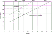
Fig. 7 is used for figure that the method for life of predicting thermoelectric generation module through Arrhenius model is described.In Fig. 7, the transverse axis of downside representes that the inverse to absolute temperature T multiply by 10000 and the value that obtains, the transverse axis of upside represent the temperature corresponding with the transverse axis of downside (℃), the longitudinal axis represent thermoelectric generation module life-span (hour).At this, so-called " life-span of thermoelectric generation module " is meant from the use of thermoelectric generation module begins after the time to output power reduction by 10%.
In Fig. 7, the durability of the thermoelectric generation module that the comparative example that solid line is represented to calculate according to measured value (black circle seal) is related.According to Arrhenius model, the life-span L of thermoelectric generation module is represented as shown in the formula (1).
L=L
0·exp(Ea/RT)…(1)
In formula (1), R is a gas constant, and it is on Boltzmann constant, to multiply by Avogadro's number and the value that obtains.
According to the measured value (black circle seal) of the related thermoelectric generation module of comparative example, can obtain the normalisation coefft L in the formula (1) as follows
0With activation energy Ea.
L
0=4.79×10
-8
Ea=110kJ/mol
When life-span of the related thermoelectric generation module of comparative example in nickel when the diffusion of solder layer limits, activation energy Ea representes to form diffusion preventing layer 72 shown in Figure 2 or 41 nickel spreads and the energy of needs in order to make in containing the solder layer of lead (Pb) more than 85%.
Shown in single-point line among Fig. 7, be made as 20 years (1.75 * 10 at target life objective with thermoelectric generation module
5Hour) situation under, the durable temperature in the maximum operation (service) temperature of the thermoelectric generation module that comparative example is related is about 190 ℃.But the thermoelectric generation module that has adopted the thermoelectric material that bismuth-tellurium (Bi-Te) is is to the maximum in the temperature (Th) of high-temperature portion under the temperature environment of 280 ℃ of that kind to be used, and therefore, is made as 20 years (1.75 * 10 at the target life objective with thermoelectric generation module
5Hour) under the above situation, preferred diffusion prevents that the durable temperature of layer is made as more than 280 ℃.
In Fig. 7, dotted line is represented the durability of the target of thermoelectric generation module.According to the durability of target, when target life objective was made as 20 years, the durable temperature of thermoelectric generation module was about 280 ℃.For this reason, activation energy Ea need be made as more than about 130kJ/mol.
Like Fig. 3 and shown in Figure 5, in first and second execution mode of the present invention, with solder layer 80 in abutting connection be provided with the diffusion preventing layer 73 and 42 that the interphase by nickel-Xi forms.Thereby, the activation energy of replacement nickel, and the activation energy of the interphase of nickel-Xi becomes problem.As the interphase of nickel-Xi, mainly generate Ni
3Sn
4, generate Ni in addition
3Sn and Ni
3Sn
2The enthalpy of formation when generating these interphases by nickel is described below.
Ni
3Sn:-24.9kJ/mol
Ni
3Sn
2:-34.6kJ/mol
Ni
3Sn
4:-24.0kJ/mol
(source: H.Flandorfer et al.; " Interfaces in lead-free solder alloys:Enthalpy of formation of binary Ag-Sn; Cu-Sn and Ni-Sn intermetallic compounds "; Thermochimica Acta Vol.459,1July 2007, pp.34-39)
Fig. 8 is the figure that the activation energy that needs to the scolder diffusion with the activation energy that needs to the scolder diffusion for the nickel that makes monomer with for the nickel of the interphase that makes formation nickel-Xi compares expression.In Fig. 8, transverse axis is represented reaction coordinate, and the longitudinal axis is represented energy (kJ/mol).At this, as the interphase of nickel-Xi, with Ni
3Sn
4For example describes.
As shown in Figure 8, the energy E 1 of needs is 110kJ/mol in order in containing the solder layer of lead (Pb) more than 85%, to spread nickel (Ni).On the other hand, generate Ni by nickel (Ni)
3Sn
4The time the enthalpy of formation be-24kJ/mol, so Ni
3Sn
4Be in energy state than the poor Δ H=24kJ/mol of the low enthalpy of formation of nickel monomer.Thereby, Ni
3Sn
4Be broken down into nickel (Ni) and tin (Sn), the energy E 2 that needs for nickel (Ni) is spread in solder layer is 134kJ/mol.
This value likens to about 130kJ/mol of the desired value of the activation energy Ea that explains with reference to figure 7 is big, and therefore, the durable temperature in the time of can the target life objective of thermoelectric generation module being 20 years is set in more than 280 ℃.As the interphase of nickel-Xi, generating Ni
3Sn
4Ni in addition
3Sn or Ni
3Sn
2Situation under, it is big that the poor Δ H of the enthalpy of formation further becomes, and therefore, even if under identical durable temperature, target life objective prolonged or durable temperature is improved.
Then, spreading caused performance degradation about the copper of electrode to thermoelectric generation elements describes.
Fig. 9 is that the part of thermoelectric generation module that comparative example is related is amplified the cutaway view of expression.In Fig. 9,, show P type element 20 as the example of thermoelectric generation elements.In addition, (a) of Fig. 9 shows the initial condition of thermoelectric generation module, and (b) of Fig. 9 schematically shows the state of the thermoelectric generation module after long-time placement the under the environment of high temperature.
Shown in Fig. 9 (a), in this thermoelectric generation module, on thermoelectric generation elements (P type element) 20, be formed with diffusion preventing layer 71 by molybdenum (Mo), on diffusion preventing layer 71, be formed with diffusion preventing layer 72 by nickel (Ni).On the other hand, be formed with diffusion preventing layer 41 on the surface of the electrode 40 that forms by copper (Cu) by nickel (Ni).And then the solder layer 80 of diffusion preventing layer 72 and diffusion preventing layer 41 composition through having 98%Pb-2%Sn engages.Need to prove that in this comparative example, solder layer 80 projects to the side of diffusion preventing layer 71 and the side of thermoelectric generation elements, and contacts with thermoelectric generation elements.
But; When placing for a long time under the related environment of thermoelectric generation module at high temperature of comparative example, shown in Fig. 9 (b), the nickel that forms diffusion preventing layer 72 and 41 spreads in solder layer 80; Nickel plating is local to disappear, and solder layer 80 directly contacts with diffusion preventing layer 71 and electrode 40.Under such state, shown in the arrow among the figure, the copper of electrode 40 spreads in solder layer 80, and then, in solder layer 80, become the copper that kind as shown in the figure more than the solid solution limit, might be to the side or the diffusion inside of thermoelectric generation elements.Especially, project at solder layer 80 diffusion preventing layer 71 side and thermoelectric generation elements the side and with situation that thermoelectric generation elements contacts under, copper is easily to the side or the diffusion inside of thermoelectric generation elements.
When copper during to the diffusion inside of thermoelectric generation elements, the resistance value of N type element 30 (Fig. 1) reduces, but the resistance value of P type element 20 increases greatlyyer, and therefore, the integral body of the resistance value of thermoelectric generation module increases, and the output power of thermoelectric generation module reduces.The temperature of the environment that this phenomenon is placed in thermoelectric generation module shows significantly more when high more.
Figure 10 is the cutaway view of the structure of thermoelectric generation elements that P type and N type are arranged of engaging respectively in the related thermoelectric generation module of expression first execution mode of the present invention and electrode.Shown in figure 10; In this thermoelectric generation module; Be formed with diffusion preventing layer 71 on the two sides of P type element 20 and N type element 30 (upper surface among the figure and lower surface) by molybdenum (Mo), be formed with diffusion preventing layer 73 by the interphase of nickel-Xi (Ni-Sn) at diffusion preventing layer 71 and face thermoelectric generation elements side opposition side.
On the other hand, be formed with diffusion preventing layer 42 at the face of the side of thermoelectric generation elements at least of the electrode 40 that forms by copper (Cu) by the interphase of nickel-Xi (Ni-Sn).Especially, in Figure 10, show the whole lip-deep example that diffusion preventing layer 42 is formed on electrode 40.And then diffusion preventing layer 73 engages through containing the solder layer 80 of lead (Pb) more than 85% with diffusion preventing layer 42.Need to prove, with the variation of first execution mode likewise, also can form solder bonds layer 74 and 43 by tin (Sn).
According to such structure, even if thermoelectric generation module long-time placement under the environment of high temperature, nickel also is inhibited to the diffusion of solder layer 80.Its reason is; As previous illustrated; The interphase that forms the nickel-Xi (Ni-Sn) of diffusion preventing layer 73 and 42 needs energy when being decomposed into nickel (Ni) and tin (Sn); So for the nickel that constitutes this interphase is spread in scolder, with the nickel of monomer in scolder, spread compare need be bigger energy.Consequently, can prevent that the copper of electrode 40 from spreading in solder layer 80, thereby can prevent side or the diffusion inside of copper to P type element 20 or N type element 30.
Figure 11 is the cutaway view of the structure of thermoelectric generation elements that P type and N type are arranged of engaging respectively in the related thermoelectric generation module of expression second execution mode of the present invention and electrode.Shown in figure 11; In this thermoelectric generation module; Be formed with diffusion preventing layer 71 on the two sides of P type element 20 and N type element 30 (upper surface among the figure and lower surface) by molybdenum (Mo); Be formed with diffusion preventing layer 72 with face thermoelectric generation elements side opposition side by nickel (Ni) diffusion preventing layer 71, and then, be formed with diffusion preventing layer 73 at diffusion preventing layer 72 and faces diffusion preventing layer 71 side opposition side by the interphase of nickel-Xi (Ni-Sn).
On the other hand; Face in the side of thermoelectric generation elements at least of the electrode 40 that is formed by copper (Cu) is formed with diffusion preventing layer 41 by nickel (Ni), is formed with diffusion preventing layer 42 at diffusion preventing layer 41 and the face electrode side opposition side by the interphase of nickel-Xi (Ni-Sn).Especially, in Figure 11, show the whole lip-deep example that diffusion preventing layer 41 and 42 is formed on electrode 40.And then diffusion preventing layer 73 engages through containing the solder layer 80 of lead (Pb) more than 85% with diffusion preventing layer 42.Need to prove, with the variation of second execution mode likewise, also can form solder bonds layer 74 and 43 by tin (Sn).
According to such structure, because the existence of diffusion preventing layer 73 and 42, the diffusion that forms the nickel of diffusion preventing layer 72 and 41 is inhibited.Through suppressing the diffusion of nickel, prevent that the copper of electrode 40 from spreading in solder layer 80, thereby can prevent side or the diffusion inside of copper to P type element 20 or N type element 30 to solder layer 80.
Then, about adopt experimental sample confirmed nickel diffusion experimental result and describe based on the effect of improving of the present invention.
Figure 12 is the cutaway view of experimental sample A of the structure of an expression part of having simulated the related thermoelectric generation module of comparative example.(a) of Figure 12 shows the initial condition of experimental sample A, and (b) of Figure 12 schematically shows the state of the experimental sample A after long-time placement the under the environment of high temperature.In addition, Figure 13 is the microphotograph of the experimental sample A after long-time placement the under the environment of high temperature.
Shown in Figure 12 (a), in experimental sample A, on the electrode 90 that forms by copper (Cu), be formed with diffusion preventing layer 91 by nickel (Ni).Prepare two such electrodes, diffusion preventing layer 91 engages through solder layer 100 each other opposed to each other.
When placing for a long time under the environment of experimental sample A at high temperature, shown in Figure 12 (b), the nickel that forms diffusion preventing layer 91 spreads in solder layer 100, and solder layer 100 directly contacts with electrode 90 in the zone of a part.
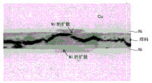
Figure 13 shows at the experimental sample A of 280 ℃ of held of temperature after 1000 hours.The 98%Pb-2%Sn that consists of at scolder that this adopted.Shown in figure 13ly know, nickel in the zone of a part (Ni) diffusion, the layer of nickel (Ni) disappears.Consequently, solder layer directly contacts with electrode, and the copper of electrode (Cu) spreads in solder layer.
Figure 14 is the cutaway view of experimental sample B of the structure of an expression part of having simulated the related thermoelectric generation module of second execution mode of the present invention.(a) of Figure 14 shows the initial condition of experimental sample B, and (b) of Figure 14 schematically shows the state of the experimental sample B after long-time placement the under the environment of high temperature.In addition, Figure 15 is the microphotograph of the experimental sample B after long-time placement the under the environment of high temperature.
Shown in Figure 14 (a), in experimental sample B, on the electrode 90 that forms by copper (Cu), be formed with diffusion preventing layer 91, and then the interphase by nickel-Xi (Ni-Sn) on diffusion preventing layer 91 is formed with diffusion preventing layer 92 by nickel (Ni).Prepare two such electrodes, diffusion preventing layer 92 engages through solder layer 100 each other opposed to each other.
Even if experimental sample B is long-time the placement under the environment of high temperature, also such shown in Figure 14 (b), the diffusion in solder layer 100 of nickel that is contained in the nickel of formation diffusion preventing layer 91 or the diffusion preventing layer 92.
Figure 15 shows at the experimental sample B of 280 ℃ of held of temperature after 1000 hours.The 98%Pb-2%Sn that consists of at scolder that this adopted.Shown in figure 15ly know that the layer of nickel (Ni) and the layer of nickel-Xi (Ni-Sn) are kept.Consequently, solder layer does not directly contact with electrode, so the copper of electrode (Cu) can not spread in solder layer.
Figure 16 is used for the figure that the variation to the output power of the related thermoelectric generation module of the related thermoelectric generation module of second execution mode of the present invention and comparative example compares.In Figure 16, transverse axis represented to use thermoelectric generation module time (hour), the longitudinal axis is represented to have carried out standardized output power with initial output.The 98%Pb-2%Sn that consists of at scolder that this adopted.In addition, the temperature of the high-temperature portion of thermoelectric generation module (Th) is 280 ℃, and the temperature (Tc) of the low-temp. portion of the thermoelectric generation module of this moment is 30 ℃.
Shown in figure 16; The output power of the thermoelectric generation module that comparative example is related begins about 1500 hours, to reduce by 10% from use; With respect to this, the output power of the thermoelectric generation module that second execution mode of the present invention is related changes slightly and chronicity is stable.
[utilizability on the industry]
Utilize in the thermoelectric generation module that the present invention can utilize temperature difference to generate electricity adopting thermoelectric generation elements.
Claims (7)
1. thermoelectric generation module comprises:
Thermoelectric generation elements;
Be configured in the surface of said thermoelectric generation elements, and the first diffusion preventing layer that constitutes by molybdenum (Mo);
Be configured in the said first diffusion preventing layer and face said thermoelectric generation elements side opposition side, and the second diffusion preventing layer that constitutes by the interphase of nickel-Xi (Ni-Sn);
Electrode;
Be configured in the surface of said electrode, and the 3rd diffusion preventing layer that constitutes by the interphase of nickel-Xi (Ni-Sn);
The said second diffusion preventing layer is engaged with said the 3rd diffusion preventing layer, and contain the solder layer of lead (Pb) more than 85%.
2. thermoelectric generation module as claimed in claim 1 wherein, also comprises:
Be configured between said first diffusion preventing layer and the said second diffusion preventing layer, and the 4th diffusion preventing layer that constitutes by nickel (Ni);
Be configured between said the 3rd diffusion preventing layer and the said electrode, and the 5th diffusion preventing layer that constitutes by nickel (Ni).
3. thermoelectric generation module as claimed in claim 1 wherein, also comprises:
Be configured between said second diffusion preventing layer and the said solder layer, and the first solder bonds layer that constitutes by tin (Sn);
Be configured between said solder layer and said the 3rd diffusion preventing layer, and the second solder bonds layer that constitutes by tin (Sn).
4. thermoelectric generation module as claimed in claim 2 wherein, also comprises:
Be configured between said second diffusion preventing layer and the said solder layer, and the first solder bonds layer that constitutes by tin (Sn);
Be configured between said solder layer and said the 3rd diffusion preventing layer, and the second solder bonds layer that constitutes by tin (Sn).
5. like each described thermoelectric generation module in the claim 1~4, wherein,
Said electrode is formed by copper (Cu).
6. like claim 1 or 3 described thermoelectric generation module, wherein,
Said electrode is formed by copper (Cu), and said the 3rd diffusion preventing layer is formed on the whole surface of said electrode.
7. like claim 2 or 4 described thermoelectric generation module, wherein,
Said electrode is formed by copper (Cu), and said the 5th diffusion preventing layer and said the 3rd diffusion preventing layer are formed on the whole surface of said electrode.
Applications Claiming Priority (3)
| Application Number | Priority Date | Filing Date | Title |
|---|---|---|---|
| JP2010-036474 | 2010-02-22 | ||
| JP2010036474A JP5545964B2 (en) | 2010-02-22 | 2010-02-22 | Thermoelectric module |
| PCT/JP2011/053596 WO2011102498A2 (en) | 2010-02-22 | 2011-02-14 | Thermoelectric generation module |
Publications (2)
| Publication Number | Publication Date |
|---|---|
| CN102754230A true CN102754230A (en) | 2012-10-24 |
| CN102754230B CN102754230B (en) | 2015-05-06 |
Family
ID=44483429
Family Applications (1)
| Application Number | Title | Priority Date | Filing Date |
|---|---|---|---|
| CN201180009621.0A Expired - Fee Related CN102754230B (en) | 2010-02-22 | 2011-02-14 | Thermoelectric generation module |
Country Status (4)
| Country | Link |
|---|---|
| US (1) | US9559281B2 (en) |
| JP (1) | JP5545964B2 (en) |
| CN (1) | CN102754230B (en) |
| WO (1) | WO2011102498A2 (en) |
Cited By (7)
| Publication number | Priority date | Publication date | Assignee | Title |
|---|---|---|---|---|
| CN103531704A (en) * | 2013-10-31 | 2014-01-22 | 中国科学院上海硅酸盐研究所 | Electrode and packaging material for skutterudite thermoelectric unicouple component and step method connection technology |
| CN104103749A (en) * | 2013-04-10 | 2014-10-15 | 中国钢铁股份有限公司 | Multilayer thermoelectric module and method for manufacturing same |
| CN105359285A (en) * | 2013-07-09 | 2016-02-24 | Kelk株式会社 | Thermoelectric generation module |
| CN105637662A (en) * | 2013-08-30 | 2016-06-01 | Kelk株式会社 | Thermoelectric power generation module |
| CN104467536B (en) * | 2014-12-11 | 2016-09-14 | 浙江亿谷电子科技有限公司 | A kind of thermoelectric power generation chip |
| CN108550688A (en) * | 2018-05-24 | 2018-09-18 | 中国科学院上海硅酸盐研究所 | A kind of thermo-electric device with adaptive connection layer |
| CN112805842A (en) * | 2018-10-05 | 2021-05-14 | 株式会社Kelk | Thermoelectric module |
Families Citing this family (16)
| Publication number | Priority date | Publication date | Assignee | Title |
|---|---|---|---|---|
| TWI446603B (en) * | 2010-12-29 | 2014-07-21 | Ind Tech Res Inst | Thermoelectric module and method of manufacturing the same |
| CN103187519B (en) * | 2011-12-30 | 2016-02-03 | 财团法人工业技术研究院 | Electrothermal module and manufacture method thereof |
| TWI605620B (en) * | 2011-12-30 | 2017-11-11 | 財團法人工業技術研究院 | Thermoelectric module and method of fabricating the same |
| CN102664193A (en) * | 2012-04-01 | 2012-09-12 | 京东方科技集团股份有限公司 | Conductive structure, manufacturing method thereof, thin film transistor, array substrate, and display device |
| US8796849B2 (en) * | 2012-10-22 | 2014-08-05 | Taiwan Semiconductor Manufacturing Company, Ltd. | Metal bump joint structure |
| FR3000299B1 (en) * | 2012-12-20 | 2016-02-05 | Valeo Systemes Thermiques | ASSEMBLY COMPRISING AN ELECTRIC THERMO ELEMENT AND ELECTRICAL CONNECTION MEANS OF SAID THERMO ELECTRIC ELEMENT, MODULE AND THERMO ELECTRICAL DEVICE COMPRISING SUCH AN ASSEMBLY. |
| US20140261606A1 (en) * | 2013-03-15 | 2014-09-18 | Avx Corporation | Thermoelectric generator |
| JP6171513B2 (en) * | 2013-04-10 | 2017-08-02 | 日立化成株式会社 | Thermoelectric conversion module and manufacturing method thereof |
| JP6122736B2 (en) * | 2013-08-30 | 2017-04-26 | 株式会社Kelk | Thermoelectric generator module |
| KR101635638B1 (en) * | 2013-10-17 | 2016-07-01 | 주식회사 엘지화학 | Thermoelectric materials and their manufacturing method |
| JP2018509749A (en) * | 2014-12-31 | 2018-04-05 | アルファベット エナジー インコーポレイテッドAlphabet Energy,Inc. | Electrical and thermal contact for bulk tetrahedral copper ore and methods for its manufacture |
| JP2017107925A (en) * | 2015-12-08 | 2017-06-15 | 日立化成株式会社 | Thermoelectric conversion module and manufacturing method therefor |
| JP6404983B2 (en) * | 2017-04-05 | 2018-10-17 | 株式会社Kelk | Thermoelectric module |
| KR102429504B1 (en) * | 2017-12-18 | 2022-08-05 | 현대자동차주식회사 | Method for manufacturing thermoelectric module |
| KR102363224B1 (en) * | 2020-07-29 | 2022-02-16 | 엘티메탈 주식회사 | Thermoelectric material having multi-diffusion barrier layer and thermoelectric device comprising the same |
| US20230062478A1 (en) * | 2021-08-26 | 2023-03-02 | Birmingham Technologies, Inc. | Energy Conversion Device, Apparatus and Related Methods |
Citations (5)
| Publication number | Priority date | Publication date | Assignee | Title |
|---|---|---|---|---|
| JPH10135523A (en) * | 1996-10-25 | 1998-05-22 | Thermo Electric Dev:Kk | Thermoelectric device |
| CN1612371A (en) * | 2003-10-29 | 2005-05-04 | 京瓷株式会社 | Thermoelectric inverting model |
| JP2008010612A (en) * | 2006-06-29 | 2008-01-17 | Komatsu Ltd | Thermoelectric element, its manufacturing method, and thermoelectric module |
| CN101447548A (en) * | 2008-12-26 | 2009-06-03 | 中国科学院上海硅酸盐研究所 | Manufacturing method of thermo-electric device |
| JP2009231317A (en) * | 2008-03-19 | 2009-10-08 | Komatsu Ltd | Thermoelectric module |
Family Cites Families (9)
| Publication number | Priority date | Publication date | Assignee | Title |
|---|---|---|---|---|
| GB1033018A (en) * | 1963-01-21 | 1966-06-15 | Rue Frigistor S A De | Thermoelectric unit and method of formation thereof |
| US4853296A (en) | 1986-10-22 | 1989-08-01 | Toppan Printing Co., Ltd. | Electrode plate for color display device |
| JPS6480932A (en) * | 1987-09-22 | 1989-03-27 | Toppan Printing Co Ltd | Electrode plate for display device |
| JP3650141B2 (en) * | 1993-11-18 | 2005-05-18 | Tdk株式会社 | permanent magnet |
| JP4614528B2 (en) * | 2000-11-29 | 2011-01-19 | 京セラ株式会社 | Wiring board manufacturing method |
| JP2003037301A (en) * | 2001-07-23 | 2003-02-07 | Komatsu Ltd | Thermoelectric module and its manufacturing method |
| JP2003282974A (en) * | 2002-03-26 | 2003-10-03 | Yamaha Corp | Thermoelectric conversion module |
| JP2004140250A (en) * | 2002-10-18 | 2004-05-13 | Kyocera Corp | Ceramic substrate for thermoelectric exchanging module |
| JP2005340565A (en) * | 2004-04-27 | 2005-12-08 | Kyocera Corp | Ceramic substrate for thermoelectric exchange module |
-
2010
- 2010-02-22 JP JP2010036474A patent/JP5545964B2/en active Active
-
2011
- 2011-02-14 CN CN201180009621.0A patent/CN102754230B/en not_active Expired - Fee Related
- 2011-02-14 WO PCT/JP2011/053596 patent/WO2011102498A2/en active Application Filing
- 2011-02-14 US US13/579,382 patent/US9559281B2/en active Active
Patent Citations (5)
| Publication number | Priority date | Publication date | Assignee | Title |
|---|---|---|---|---|
| JPH10135523A (en) * | 1996-10-25 | 1998-05-22 | Thermo Electric Dev:Kk | Thermoelectric device |
| CN1612371A (en) * | 2003-10-29 | 2005-05-04 | 京瓷株式会社 | Thermoelectric inverting model |
| JP2008010612A (en) * | 2006-06-29 | 2008-01-17 | Komatsu Ltd | Thermoelectric element, its manufacturing method, and thermoelectric module |
| JP2009231317A (en) * | 2008-03-19 | 2009-10-08 | Komatsu Ltd | Thermoelectric module |
| CN101447548A (en) * | 2008-12-26 | 2009-06-03 | 中国科学院上海硅酸盐研究所 | Manufacturing method of thermo-electric device |
Cited By (12)
| Publication number | Priority date | Publication date | Assignee | Title |
|---|---|---|---|---|
| CN104103749A (en) * | 2013-04-10 | 2014-10-15 | 中国钢铁股份有限公司 | Multilayer thermoelectric module and method for manufacturing same |
| CN104103749B (en) * | 2013-04-10 | 2016-12-28 | 中国钢铁股份有限公司 | Multilayer thermoelectric module and method for manufacturing same |
| CN105359285A (en) * | 2013-07-09 | 2016-02-24 | Kelk株式会社 | Thermoelectric generation module |
| CN105637662A (en) * | 2013-08-30 | 2016-06-01 | Kelk株式会社 | Thermoelectric power generation module |
| CN105637662B (en) * | 2013-08-30 | 2019-07-05 | Kelk株式会社 | Thermoelectric generation module |
| CN110246954A (en) * | 2013-08-30 | 2019-09-17 | Kelk株式会社 | Thermoelectric generation module |
| CN103531704A (en) * | 2013-10-31 | 2014-01-22 | 中国科学院上海硅酸盐研究所 | Electrode and packaging material for skutterudite thermoelectric unicouple component and step method connection technology |
| CN103531704B (en) * | 2013-10-31 | 2020-01-21 | 中国科学院上海硅酸盐研究所 | Electrode and packaging material for skutterudite thermoelectric single couple element and one-step connection process |
| CN104467536B (en) * | 2014-12-11 | 2016-09-14 | 浙江亿谷电子科技有限公司 | A kind of thermoelectric power generation chip |
| CN108550688A (en) * | 2018-05-24 | 2018-09-18 | 中国科学院上海硅酸盐研究所 | A kind of thermo-electric device with adaptive connection layer |
| CN112805842A (en) * | 2018-10-05 | 2021-05-14 | 株式会社Kelk | Thermoelectric module |
| US11903316B2 (en) | 2018-10-05 | 2024-02-13 | Kelk Ltd. | Thermoelectric module |
Also Published As
| Publication number | Publication date |
|---|---|
| US9559281B2 (en) | 2017-01-31 |
| CN102754230B (en) | 2015-05-06 |
| JP2011171668A (en) | 2011-09-01 |
| WO2011102498A2 (en) | 2011-08-25 |
| US20130032188A1 (en) | 2013-02-07 |
| JP5545964B2 (en) | 2014-07-09 |
| WO2011102498A3 (en) | 2011-10-20 |
Similar Documents
| Publication | Publication Date | Title |
|---|---|---|
| CN102754230B (en) | Thermoelectric generation module | |
| KR101773869B1 (en) | Thermoelectric generation module | |
| JP4912964B2 (en) | Thermoelectric conversion module | |
| KR101932979B1 (en) | Thermoelectric power generation module | |
| US20080023057A1 (en) | Thermoelectric Conversion Module, and Thermoelectric Power Generating Device and Method, Exhaust Heat Recovery System, Solar Heat Utilization System, and Peltier Cooling and Heating System, Provided Therewith | |
| CN105637662A (en) | Thermoelectric power generation module | |
| JP5243823B2 (en) | Thermoelectric module | |
| KR20070083845A (en) | Thermoelectric material contact | |
| JP6404983B2 (en) | Thermoelectric module | |
| US11903316B2 (en) | Thermoelectric module | |
| JP2021517366A (en) | Thermoelectric conversion device and method for manufacturing it | |
| JP2016009779A (en) | Thermoelectric conversion module | |
| RU2781494C2 (en) | Thermoelectric conversion device and its manufacturing method | |
| WO2020071529A1 (en) | Thermoelectric module | |
| US3506498A (en) | Thermoelectric device including conductive granules for obtaining low resistance bonds | |
| Jie et al. | Contacts for Skutterudites | |
| JP2005050862A (en) | Thermoelectric conversion module | |
| Ngan et al. | Bismuth Telluride Modules | |
| Byrnes et al. | High efficiency thermoelectric power conversion |
Legal Events
| Date | Code | Title | Description |
|---|---|---|---|
| C06 | Publication | ||
| PB01 | Publication | ||
| C10 | Entry into substantive examination | ||
| SE01 | Entry into force of request for substantive examination | ||
| C14 | Grant of patent or utility model | ||
| GR01 | Patent grant | ||
| CF01 | Termination of patent right due to non-payment of annual fee | ||
| CF01 | Termination of patent right due to non-payment of annual fee |
Granted publication date: 20150506 Termination date: 20210214 |