CN102396112B - Current terminal structure of superconducting wire material and superconducting cable having this current terminal structure - Google Patents
Current terminal structure of superconducting wire material and superconducting cable having this current terminal structure Download PDFInfo
- Publication number
- CN102396112B CN102396112B CN2010800163827A CN201080016382A CN102396112B CN 102396112 B CN102396112 B CN 102396112B CN 2010800163827 A CN2010800163827 A CN 2010800163827A CN 201080016382 A CN201080016382 A CN 201080016382A CN 102396112 B CN102396112 B CN 102396112B
- Authority
- CN
- China
- Prior art keywords
- superconducting wire
- layer
- superconducting
- mentioned
- current terminal
- Prior art date
- Legal status (The legal status is an assumption and is not a legal conclusion. Google has not performed a legal analysis and makes no representation as to the accuracy of the status listed.)
- Active
Links
Images


Classifications
-
- H—ELECTRICITY
- H02—GENERATION; CONVERSION OR DISTRIBUTION OF ELECTRIC POWER
- H02G—INSTALLATION OF ELECTRIC CABLES OR LINES, OR OF COMBINED OPTICAL AND ELECTRIC CABLES OR LINES
- H02G15/00—Cable fittings
- H02G15/34—Cable fittings for cryogenic cables
-
- H—ELECTRICITY
- H01—ELECTRIC ELEMENTS
- H01R—ELECTRICALLY-CONDUCTIVE CONNECTIONS; STRUCTURAL ASSOCIATIONS OF A PLURALITY OF MUTUALLY-INSULATED ELECTRICAL CONNECTING ELEMENTS; COUPLING DEVICES; CURRENT COLLECTORS
- H01R4/00—Electrically-conductive connections between two or more conductive members in direct contact, i.e. touching one another; Means for effecting or maintaining such contact; Electrically-conductive connections having two or more spaced connecting locations for conductors and using contact members penetrating insulation
- H01R4/58—Electrically-conductive connections between two or more conductive members in direct contact, i.e. touching one another; Means for effecting or maintaining such contact; Electrically-conductive connections having two or more spaced connecting locations for conductors and using contact members penetrating insulation characterised by the form or material of the contacting members
- H01R4/68—Connections to or between superconductive connectors
-
- H—ELECTRICITY
- H10—SEMICONDUCTOR DEVICES; ELECTRIC SOLID-STATE DEVICES NOT OTHERWISE PROVIDED FOR
- H10N—ELECTRIC SOLID-STATE DEVICES NOT OTHERWISE PROVIDED FOR
- H10N60/00—Superconducting devices
- H10N60/80—Constructional details
-
- Y—GENERAL TAGGING OF NEW TECHNOLOGICAL DEVELOPMENTS; GENERAL TAGGING OF CROSS-SECTIONAL TECHNOLOGIES SPANNING OVER SEVERAL SECTIONS OF THE IPC; TECHNICAL SUBJECTS COVERED BY FORMER USPC CROSS-REFERENCE ART COLLECTIONS [XRACs] AND DIGESTS
- Y02—TECHNOLOGIES OR APPLICATIONS FOR MITIGATION OR ADAPTATION AGAINST CLIMATE CHANGE
- Y02E—REDUCTION OF GREENHOUSE GAS [GHG] EMISSIONS, RELATED TO ENERGY GENERATION, TRANSMISSION OR DISTRIBUTION
- Y02E40/00—Technologies for an efficient electrical power generation, transmission or distribution
- Y02E40/60—Superconducting electric elements or equipment; Power systems integrating superconducting elements or equipment
Abstract
A superconductor has one or more layers of a superconducting wire material including a superconducting layer formed on a substrate and wound around a former. In the superconductor, the first layer superconducting wire material wound immediately above the former is arranged so that the substrate side becomes outside and the superconducting layer side becomes inside. In a current terminal structure of the superconductor, a surface of the superconducting layer at an end of the first layer superconducting wire material, the surface being directed toward the inside, and part of a surface of the superconducting layer of a connection superconducting wire material, the surface being directed toward the outside, are faced and connected to each other.
Description
Technical field
The present invention relates to the current terminal structure of superconducting wire and possess the hyperconductive cable of this current terminal structure.
Background technology
Generally speaking, superconductor has at iron core (former: mould) upper structure of rolling up the superconducting wire that the multilayer band shape is arranged.The superconducting wire of the film class of using has following structure: form via intermediate layer the superconducting layer consisted of for example ReBCO (Re-Ba-Cu-O, Re are rare earth metals) on substrate, and form the stabilized zone consisted of silver thereon.
When current flowing in such superconductor, for the heating of the connecting portion that in the superconducting layer that makes each superconducting wire, current flowing and making is connected with the ampere wires of supplying with electric current equably diminishes, the contact resistance of current terminal section must be lower.
There is table and inner in superconducting wire, and usually, the connection at the current terminal place makes superconducting layer one side become the outside or table side.Become when table when connecting into substrate-side, because substrate has high resistance, so will produce larger Joule heat, efficiency is lower.
While on using the surface of YBCO (Y-Ba-Cu-O) layer as the YBCO superconducting wire of superconducting layer, applying vertical magnetic field, can produce larger A.C.power loss.That is, if superconducting wire, the Lorentz force of the direction that invade and pining force balance are invaded in Bian great , magnetic field, magnetic field.When producing interchange, magnetic field periodically changes and the reverse action of pining force, therefore can produce A.C.power loss.
But, when the surface at superconducting wire applies parallel magnetic field, because superconducting layer is that 1 μ m left and right is very thin, so the zone that magnetic field is invaded is thinner, A.C.power loss is very little.For example,, when with the YBCO superconducting wire, manufacturing cable, owing to being mainly parallel magnetic field, so that A.C.power loss can become is very little.But, because the width of actual superconducting wire is limited, so there is gap in the cross section of cable between wire rod, form the situation in this attraction magnetic field, gap.And, at the composition of this part generation vertical magnetic field, just can share most A.C.power loss (for example,, with reference to non-patent literature 1).
When the YBCO superconducting wire is applied to power equipment, reduce like this vertical magnetic field extremely important.
On the other hand, when substrate has magnetic, because magnetic field is attracted by Magnetic Substrate, so describe the complicated magnetic line of force.That is, in the end of wire rod flux concentration, more at this part vertical magnetic field, loss is large (for example,, with reference to non-patent literature 1).
Fig. 7 illustrates the current terminal section of common multilayer hyperconductive cable.In Fig. 4, around mould 21, helically is wound with the 1st superconducting wire 22 of the 1st layer and the 2nd superconducting wire 23 of the 2nd layer.Now, the 1st superconducting wire 22 of the 1st layer consists of substrate 22a and the superconducting layer 22b be formed on this substrate 22a, and the 2nd superconducting wire 23 of the 2nd layer consists of substrate 23a and the superconducting layer 23b be formed on this substrate 23a.
The the 1st and the 2nd superconducting wire 22,23 all is configured to superconducting layer 22b, 23b becomes table side (outside).The end of the 1st and the 2nd superconducting wire 22,23 of configuration is cut by ladder like this, by being welded and fixed section 24, forms integrated current terminal section (for example,, with reference to patent documentation 1).
According to such current terminal section, contact resistance is very little, to the degree of the shunting of each superconducting layer, by the winding screw of superconducting layer, is decided, and by adjusting this winding screw, just can realize the almost shunting of equalization.
Fig. 8 illustrates the current terminal section of the magnetic multilayer hyperconductive cable of substrate tool.In Fig. 5, around mould 21, helically is wound with the 1st superconducting wire 22 of the 1st layer and the 2nd superconducting wire 23 of the 2nd layer.Now, by the 1st superconducting wire 22 of the 1st layer and common configuration be configured on the contrary the magnetic substrate 22a of tool side towards the outside of hyperconductive cable, the 2nd superconducting wire 23 of the 2nd layer be configured to superconducting layer 23b towards the outside of hyperconductive cable, carry out conductor, so just the impact of magnetic can be enclosed in to superconductor inside, thereby by A.C.power loss, suppress lowlyer (for example,, with reference to patent documentation 2).
But the contact resistance of the current terminal section of superconducting layer 22b when inboard (inboard) that is configured to the 1st superconducting wire 22 of the 1st layer becomes large, layers 1 and 2 is not shared same current.That is, owing to there is no enough electrode capacities, so surpass the stage of critical current Ic at the electric current when flowing through the 2nd superconducting wire 23 of the 2nd layer, can produce Joule heat, A.C.power loss can be very large.
The prior art document
Non-patent literature
Non-patent literature 1:N.Amemiya and M.Nakahata, Physica C 463-465 (2007) 775-780
Patent documentation
Patent documentation 1: TOHKEMY 2004-87265 communique
Patent documentation 2: TOHKEMY 2008-47519 communique
Summary of the invention
The problem that invention will solve
The present invention is in view of above situation, and its purpose is to provide a kind of hyperconductive cable, the current terminal structure of the superconducting wire that its contact resistance is low, A.C.power loss is few and the hyperconductive cable that possesses this current terminal.
For solving the means of problem
In order to solve above-mentioned problem, the 1st mode of the present invention is a kind of current terminal structure of superconductor, above-mentioned superconductor is that the superconducting wire that will be formed with superconducting layer on substrate is wound around more than 1 layer and the superconductor obtained on mould, directly be wrapped in the 1st layer of superconducting wire on above-mentioned mould, with substrate-side become the outside, the superconducting layer side becomes inboard mode and is configured, it is characterized in that the connecting opposite to each other with the part be connected with the face towards the outside of the superconducting layer of superconducting wire towards inboard face of the superconducting layer of the end of above-mentioned the 1st layer of superconducting wire.
In the current terminal structure of such superconductor, on above-mentioned the 1st layer of superconducting wire with the superconducting layer side become the outside, substrate-side becomes inboard mode and is wound with the 2nd layer of superconducting wire, described current terminal structure possesses the section of being welded and fixed, and this section of being welded and fixed is used scolder to make the end of part that above-mentioned connection exposes with the superconducting layer of superconducting wire and above-mentioned the 2nd layer of superconducting wire integrated.
Now, the scolder that preferred above-mentioned connection is used with the connecting portion of superconducting wire and above-mentioned the 1st layer of superconducting wire is less than or equal to the resistivity of the scolder that the above-mentioned section of being welded and fixed uses in the resistivity under liquid-nitrogen temperature.The fusing point of the scolder that the fusing point of the scolder that in addition, preferred above-mentioned connection is used with the connecting portion of superconducting wire and above-mentioned the 1st layer of superconducting wire is used than the above-mentioned section of being welded and fixed is high.Now, above-mentioned connection with superconducting wire with the above-mentioned connecting length b that is welded and fixed section and above-mentioned the 2nd layer of superconducting wire meet the relation of b >=c with the above-mentioned connecting length c that is welded and fixed section.
The 2nd mode of the present invention is a kind of current terminal structure of superconductor, above-mentioned superconductor is that the superconducting wire that will be formed with superconducting layer on substrate is wound around more than 4 layers and the superconductor obtained on mould, the odd-level superconducting wire, becoming the outside with substrate-side, the superconducting layer side becomes inboard mode and is configured, it is characterized in that the connecting opposite to each other with the part be connected with the face towards the outside of the superconducting layer of superconducting wire towards inboard face of the superconducting layer of the end of above-mentioned odd-level superconducting wire.
The current terminal structure of such superconductor, on above-mentioned odd-level superconducting wire with the superconducting layer side become the outside, substrate-side becomes inboard mode and is wound with above-mentioned odd number and adds one deck superconducting wire, described current terminal structure possesses the section of being welded and fixed, and the end that this section of being welded and fixed is used scolder to make part that above-mentioned connection exposes with the superconducting layer of superconducting wire and above-mentioned odd number add one deck superconducting wire is integrated.
Now, the scolder that preferred above-mentioned connection is used with the connecting portion of superconducting wire and above-mentioned odd-level superconducting wire is less than or equal to the resistivity of the scolder that the above-mentioned section of being welded and fixed uses in the resistivity under liquid-nitrogen temperature.The fusing point of the scolder that the fusing point of the scolder that in addition, preferred above-mentioned connection is used with the connecting portion of superconducting wire and above-mentioned odd-level superconducting wire is used than the above-mentioned section of being welded and fixed is high.Now, above-mentioned connection with superconducting wire add one deck superconducting wire with the above-mentioned connecting length b that is welded and fixed section and above-mentioned odd number meet the relation of b >=c with the above-mentioned connecting length c that is welded and fixed section.
The 3rd mode of the present invention provides a kind of hyperconductive cable, it is characterized in that, has above current terminal structure.
The invention effect
According to the present invention, provide the current terminal structure of the superconducting wire that a kind of contact resistance is low, A.C.power loss is few and the hyperconductive cable that possesses this current terminal structure.
The accompanying drawing explanation
Fig. 1 means the profile of current terminal structure of the superconducting wire of an embodiment of the invention.
Fig. 2 means the profile of current terminal structure of the superconducting wire of other execution modes of the present invention.
Fig. 3 means the profile of current terminal structure of the superconducting wire of other execution modes of the present invention.
Fig. 4 means the profile of current terminal structure of the superconducting wire of other execution modes of the present invention.
Fig. 5 means the profile of current terminal structure of the superconducting wire of other execution modes of the present invention.
Fig. 6 A means the synoptic diagram of the step of the current terminal structure of making superconducting wire in an embodiment of the invention.
Fig. 6 B means the synoptic diagram of the step of the current terminal structure of making superconducting wire in an embodiment of the invention.
Fig. 6 C means the synoptic diagram of the step of the current terminal structure of making superconducting wire in an embodiment of the invention.
Fig. 6 D means the synoptic diagram of the step of the current terminal structure of making superconducting wire in an embodiment of the invention.
Fig. 6 E means the synoptic diagram of the step of the current terminal structure of making superconducting wire in an embodiment of the invention.
Fig. 6 F means the synoptic diagram of the step of the current terminal structure of making superconducting wire in an embodiment of the invention.
Fig. 7 means the profile of the current terminal structure of existing multilayer hyperconductive cable.
Fig. 8 means the profile of the current terminal structure of the magnetic existing multilayer hyperconductive cable of substrate tool.
Embodiment
Referring to accompanying drawing explanation embodiments of the present invention.
Fig. 1 is the profile of current terminal section of hyperconductive cable of 2 layers of structure of the 1st execution mode of the present invention.In addition, record the section of hyperconductive cable the first half in Fig. 1 (following is also same), the latter half is omitted.
In Fig. 1, spirally be wound with the 1st superconducting wire 2 of the 1st layer and the 2nd superconducting wire 3 of the 2nd layer around mould 1.Now, the 1st superconducting wire 2 of the 1st layer consists of with wire rod B with the connection be connected with its end wire rod A, this wire rod A consists of substrate 2a and the superconducting layer 2b be formed on this substrate 2a, and this connection consists of substrate 4a and the superconducting layer 4b be formed on this substrate 4a with wire rod B.In addition, the 2nd superconducting wire 3 of the 2nd layer consists of substrate 3a and the superconducting layer 3b be formed on this substrate 3a.
In the 1st superconducting wire 2, wire rod A is configured to substrate 2a becomes table side (outside), and connection is configured to superconducting layer 4b with wire rod B becomes table side (outside), and the superconducting layer 2b of wire rod A is relative with the superconducting layer 4b connected with wire rod B.In addition, the 2nd superconducting wire 3 is configured to superconducting layer 3b becomes table side (outside).
The end of the 1st superconducting wire 2 of configuration and the 2nd superconducting wire 3 is integrated by being welded and fixed section 3 like this.In addition, the integrated of end based on the 1st superconducting wire 2 and the 2nd superconducting wire 3 is described in the back and forms the concrete grammar of current terminal structure.
As constructed as above in the current terminal structure of superconducting wire, because wire rod A is configured to, substrate 2a becomes table side (outside) so A.C.power loss reduces, in addition, connect with wire rod B and be configured to the superconducting layer 2b and the superconducting layer 4b contact be connected with wire rod B that superconducting layer 4b becomes table side (outside), wire rod A, so the electric current flow through in the 1st superconducting wire 2 and the 2nd superconducting wire 3 is even, contact resistance is also low.
Now, wish in the 1st superconducting wire 2, more than the fusing point of the scolder that the fusing point of wire rod A and the scolder used in the connection be connected with wire rod B is used in being welded and fixed section 5.In addition, wish below the resistance value of resistance value under the liquid-nitrogen temperature of the scolder that is used in the section of being welded and fixed 5 under the liquid-nitrogen temperature of wire rod A and the scolder used in the connection be connected with wire rod B.In addition, temperature when liquid-nitrogen temperature means the operation of hyperconductive cable with current terminal structure etc., the 63K while specifically liquid nitrogen being used in to cold-producing medium~90K left and right.
In addition, wish to connect with wire rod B with the connecting length that is welded and fixed section 5 (stripping out length) b and the 2nd superconducting wire 3 with connecting length scolder fixed part 5 (stripping out length) c, meet b >=c.In addition, when the diameter of superconductor is 15~100mm, the value of c is normally more than 30mm, preferably 50~100mm.In addition, the value of b is normally more than 30mm, preferably 50~110mm.
Length a, connecting length b, c meet such condition, thus, even the 1st superconducting wire 2 is configured to substrate 2a, become the table side, also can realize reliably the homogenizing of electric current of the superconductor of multiple stratification.In addition, the diameter of superconductor, in the situation that Fig. 1 is the diameter that forms the layer of the 1st superconducting wire 2, in other words, is meant to be and forms the conductor diameter that is connected with the layer that connects the superconducting wire (the 1st superconducting wire 2) of using wire rod (the 2nd superconducting wire 3).
Fig. 2 is the profile of current terminal structure of hyperconductive cable of 4 layers of structure of the 2nd execution mode of the present invention.Hyperconductive cable shown in Fig. 2 is with respect to the hyperconductive cable shown in Fig. 1, has 4 layers of structure that further helically is wound with the 4th superconducting wire 7 of the 3rd superconducting wire 6 of the 3rd layer and the 4th layer.
Now, the structure of the end of the 3rd superconducting wire 6 of the 3rd layer and the 4th superconducting wire 7 of the 4th layer, except peeling off by ladder, retreat the superconducting layer 3b that is configured to make the 2nd superconducting wire 3 exposes up, identical with the structure of the end of the 2nd superconducting wire 3 of the 1st superconducting wire 2 of the 1st layer and the 2nd layer.
; the 3rd superconducting wire 6 of the 3rd layer consists of with wire rod D with the connection be connected with its end wire rod C; this wire rod C consists of substrate 6a and the superconducting layer 6b be formed on this substrate 6a, and this connection consists of substrate 8a and the superconducting layer 8b be formed on this substrate 8a with wire rod D.In addition, in the 3rd superconducting wire 6, wire rod C is configured to substrate 6a becomes table side (outside), and connection is configured to superconducting layer 8b with wire rod D becomes table side (outside), and the superconducting layer 6b of wire rod C is relative with the superconducting layer 8b be connected with wire rod D.
And then the mode that becomes table side (outside) on such the 3rd superconducting wire 6 of the 3rd layer with superconducting layer 7b disposes the 4th superconducting wire 7, the 4 superconducting wires 7 of the 4th layer and consists of substrate 7a and the superconducting layer 7b that is formed on this substrate 7a.
The end of the 1st superconducting wire the 2, the 2nd superconducting wire the 3, the 3rd superconducting wire 6 of configuration and the 4th superconducting wire 7 is integrated by being welded and fixed section 9 like this.
Now, in the 3rd superconducting wire 6, more than length (connecting length) d preferably wire rod C overlapped each other with the end be connected with wire rod D is made as 50mm, preferred scheme is for being made as 50~100mm.
In addition, preferably the 4th superconducting wire 7 and the pass with the connecting length e that the is welded and fixed section 9 connecting length f that is welded and fixed section 9 and superconducting wire D are e >=f.In addition, when the diameter of superconductor is 15~100mm, the value of f is preferably 50~100mm more than being generally 30mm.
In addition, the value of e is preferably 50~110mm more than being generally 30mm.
Connecting length d, e, f meet such condition, thus, even the 3rd superconducting wire 6 is configured to substrate 6a, become the table side, also can realize reliably the homogenizing of electric current of the superconductor of multiple stratification.
Fig. 3 is the profile of current terminal structure of hyperconductive cable of 6 layers of structure of the 3rd execution mode of the present invention.Hyperconductive cable shown in Fig. 3 is with respect to the hyperconductive cable shown in Fig. 2, has 6 layers of structure that further helically is wound with the 6th superconducting wire 14 of the 5th superconducting wire 13 of the 5th layer and the 6th layer.
Now, with the hyperconductive cable of 4 layers of structure similarly, the structure of the end of the 5th superconducting wire 13 of the 5th layer and the 6th superconducting wire 14 of the 6th layer, except peeling off by ladder to retreat, arrange so that the superconducting layer 7b of the 4th superconducting wire 7 exposes up, all identical with the structure of the end of the 2nd superconducting wire 3 of the 1st superconducting wire 2 of the 1st layer and the 2nd layer.
That is, the 5th superconducting wire 13 of the 5th layer consists of with wire rod F with the connection be connected with its end wire rod E, and this wire rod E consists of substrate and the superconducting layer be formed on this substrate, and this connection consists of substrate and the superconducting layer be formed on this substrate with wire rod F.In addition, in the 5th superconducting wire 13, wire rod E is configured to substrate becomes table side (outside), and connection is configured to superconducting layer with wire rod F becomes table side (outside), and the superconducting layer of wire rod E is relative with the superconducting layer be connected with wire rod F.
And then the mode that becomes table side (outside) on such the 5th superconducting wire 13 of the 5th layer with superconducting layer disposes the 6th superconducting wire 14, the 6 superconducting wires 14 of the 6th layer and consists of substrate and the superconducting layer that is formed on this substrate.The end of the 1st superconducting wire the 2, the 2nd superconducting wire the 3, the 3rd superconducting wire the 6, the 4th superconducting wire the 7, the 5th superconducting wire 13 of configuration and the 6th superconducting wire 14 is integrated by being welded and fixed section 15 like this.
Like this, for the superconducting wire of for example the 3rd layer, the 5th layer, the 7th layer of odd-level, be connected with by using the superconducting wire that connects with wire rod in its end, make the superconducting layer of its end integrated, just can obtain and above-mentioned same effect.Based on be welded and fixed section integrated be that carry out the end that the superconducting wire from the 1st layer is added to the superconducting wire of 1 layer to the odd number of the superiors.
Now, the odd-level superconducting wire be connected more than connecting length a with wire rod is preferably 50mm, 50~100mm preferably.In addition, wish to connect the relation that meets b >=c with the connecting length c with being welded and fixed section that adds 1 layer of superconducting wire with the connecting length b that is welded and fixed section and odd number of wire rod.In addition, when the diameter of superconductor is 15~100mm, the value of c is preferably 50~100mm more than being generally 30mm.In addition, the value of b is preferably 50~110mm more than being generally 30mm.
In addition, when the superconducting wire of odd-level comprises the magnetic substrate of tool, especially can bring into play its effect.At this, " the magnetic substrate of tool " means the metal substrate that has saturation magnetization below the ambient temperature of superconductor (representational is 77K) using, and particularly saturation magnetization in use is that 0.15T can bring into play effect of the present invention when above.In addition, as magnetic metal, specifically can list and take kicker magnet that Fe, Co, Ni etc. are representative or take these metals as basic alloy.
When the superconducting wire of odd-level comprises the magnetic substrate of tool, the superconducting wire of even level can comprise the magnetic substrate of tool, also can use and comprise the not superconducting wire (IBAD wire rod etc.) of the magnetic substrate of tool (for example, HASTELLOY (registered trade mark)).
Fig. 4 is the profile of current terminal structure of hyperconductive cable of the 3-tier architecture of the 4th execution mode of the present invention.Hyperconductive cable shown in Fig. 4 is with respect to the hyperconductive cable shown in Fig. 1, have further the 3rd helical layer shape be wound with that to comprise the not superconducting wire of the magnetic substrate of tool be the 3-tier architecture of non magnetic superconducting wire 16.
Now, the structure of the end of the non magnetic superconducting wire 16 of the 3rd layer is for by ladder, peeling off and retreat configuration, so that the superconducting layer 3b of the 2nd superconducting wire 3 exposes up.
The end of the 1st superconducting wire the 2, the 2nd superconducting wire 3 of configuration and non magnetic superconducting wire 16 is integrated by being welded and fixed section 17 like this.
Fig. 5 is the profile of current terminal structure of hyperconductive cable of 5 layers of structure of the 5th execution mode of the present invention.Hyperconductive cable shown in Fig. 5 is with respect to the hyperconductive cable shown in Fig. 2, have further the 5th helical layer shape be wound with that to comprise the not superconducting wire of the magnetic substrate of tool be 5 layers of structure of non magnetic superconducting wire 18.
Now, the structure of the end of the non magnetic superconducting wire 18 of the 5th layer is for by ladder, peeling off and retreat configuration, so that the superconducting layer 7b of the 4th superconducting wire 7 exposes up.
The end of the 1st superconducting wire the 2, the 2nd superconducting wire the 3, the 3rd superconducting wire the 6, the 4th superconducting wire 7 of configuration and non magnetic superconducting wire 18 is integrated by being welded and fixed section 19 like this.
Like this when by more than 3 layers, form and situation that outermost layer finishes with odd-level under, if use and comprise the not superconducting wire of the magnetic substrate of tool at outermost layer, do not need to connect and use superconducting wire, just the current terminal structure can be formed to obtain to compactness comparatively.
Then, with reference to Fig. 6 A~6F, illustrate the formation method of the integrated scolding tin fixed part of the superconducting layer of the end of superconductor.
At first, carry out as shown in Figure 6A ladder and peel off being spirally wrapped around the 1st on mould 1 and the 2nd superconducting wire 2,3.And, the end of the 1st and the 2nd superconducting wire 2,3 is curling and rearward extend along fixture 11.Then, as shown in Figure 6B, will connect and be configured to superconducting layer (in the drawings omit) with wire rod B and become table side (outside).
Then, connection is ground and made it level and smooth with the surface of the superconducting layer of wire rod B, coating scaling powder (flux).Scaling powder can be used the scaling powder of the resinae that does not for example add halogen.And, on the basis that has applied scaling powder, be wound around for example thin welding of thickness 0.1mm.Welding can be used the Sn-43Pb-14Bi of 165 ℃ of fusing points (liquidus curve) for example.
Then, as shown in Figure 6 C, by curling and the end of wire rod A that be positioned at the 1st superconducting wire 2 of the 1st layer at rear is unloaded from fixture 11, be disposed on welding, be wound around band and the heater pressed.More than the power supply of connection heater is heated to the fusing point of welding.If welding melts by such heating, connect with the superconducting layer of wire rod B and the superconducting layer welding of the 1st superconducting wire 2.
Then, as shown in Figure 6 D, the 2nd superconducting wire 3 of the 2nd layer is turned back on the end of the 1st superconducting wire 2 connected by welding.Now, the 2nd superconducting wire 3 stripped out to length b and the relation that length c is made as b >=c that strips out be connected with wire rod B.
For the structure meaned at this Fig. 6 D, the processing that the 1st superconducting wire 2 is electrically connected to together with the 2nd superconducting wire 3.The following describes its step.
As shown in Fig. 6 E, the reticular zone 12 that is wound around 1 layer to several layers strips out length c with being connected with wire rod B with the length b that strips out that covers the 2nd superconducting wire 3.Reticular zone 12 is woven with the metal fine of satisfactory electrical conductivity.For example, can preferably use the flat sennit line (plain stitch) of copper.
Then, the scolder of low-melting-point metal (for example, Sn-43Pb-14Bi) is melted, soaks into the mesh of reticular zone 12, make reticular zone 12 and the 2nd superconducting wire 3 and be connected the welding with wire rod B by scolder, make the end of the 2nd superconducting wire 3 of the 1st superconducting wire 2 of the 1st layer and the 2nd layer integrated.Reference number 5 means to be welded and fixed section.
As shown in Fig. 6 F, can carry out this institutional operation by following steps: for example, the part that will be covered by the reticular zone 12 of the 2nd superconducting wire 3 of the 1st superconducting wire 2 of the 1st layer and the 2nd layer is immersed in the melting solder that is contained in crucible, makes scolder be impregnated into the 1st and the 2nd superconducting wire 2,3 from reticular zone 12.In addition, can replace reticular zone 12, and use the non-netted metal fine with satisfactory electrical conductivity, be intertwined and connected by the part that strips out of wire rod B and the 2nd superconducting wire 3.
End by the 1st and the 2nd such superconducting wire 2,3 integrated, the thickness attenuation of the scolder that resistance is large is also passable, therefore can make the contact resistance of the stub area of the 1st and the 2nd superconducting wire 2,3 become very little.In addition, due to the metal fine formation current path of the satisfactory electrical conductivity that forms reticular zone 12, so the contact resistance of the end of the 1st and the 2nd superconducting wire 2,3 just becomes even.
At this, the end of the 2nd superconducting wire 3 of the 1st superconducting wire 2 of the 1st layer and the 2nd layer is integrated and form the fusing point of the scolder that is welded and fixed section 5, and the fusing point of the scolder used while preferably engaging than the wire rod A at the 1st superconducting wire 2 and wire rod B is low.The difference of this fusing point is the bigger the better, the fusing point of the scolder used while wishing to carry out wire rod A that construction temperature when integrated is no more than superconducting wire 2 with the joint that is connected with wire rod B.
In addition, the scolder used when the wire rod A of the 1st superconducting wire 2 and wire rod B engage wishes that fusing point (liquidus curve) is the low-melting-point metal below 250 ℃.As previously mentioned, connecting with on wire rod B, configuring welding, the wire rod A of the 1st superconducting wire 2 of the 1st layer is disposed on welding, more than connection is heated to the fusing point of welding with the 1st superconducting wire 2 of wire rod B and the 1st layer.Now, when heating is high temperature, because the superconducting layer connected with wire rod B and the 1st superconducting wire 2 worsens, so be preferably low-melting-point metal at the wire rod A of the 1st superconducting wire 2 with being connected the scolder that uses while engaging with wire rod B, thermal endurance from superconducting wire, preferably, below 250 ℃, be more preferably less than 200 ℃.
In addition, in following embodiment, use the scolder 1~5 of record in following table 1.In addition, the room temperature of table 1 means 25 ℃, and liquid-nitrogen temperature means 77K.
Table 1

Scolder 1:BI165 (Co., Ltd. Japan ス ペ リ ア company system)
Scolder 2: low temperature plastan 120 (the blue or green wooden メ タ Le system of Co., Ltd.)
Scolder 3:BI57 (Co., Ltd. Japan ス ペ リ ア company system)
Scolder 4:H60A (the blue or green wooden メ タ Le system of Co., Ltd.)
Scolder 5:SN100C (Co., Ltd. Japan ス ペ リ ア company system)
Embodiment
Below mean embodiments of the invention, be described more specifically the present invention and effect of the present invention.
In twisting on the mould of the wire that covers of multilayer insulation and the diameter 20mm that forms, helically is wound around the 1st layer of the 1st superconducting wire, makes substrate become table side (outside).In addition, as the 1st and the 2nd superconducting wire, use the YBCO wire rod that is formed with the YBCO layer on the substrate formed by the magnetic Ni5W of tool.
Then, helically is wound around the 2nd superconducting wire of the 2nd layer with the 1st superconducting wire same structure of the 1st layer, makes the face of superconducting layer become table side (outside).
Afterwards, according to the method shown in Fig. 3, use the strip-shaped solder formed with the scolder 1~5 of putting down in writing in wire rod, reticular zone and table 1 by connecting, make the 1st and the end of the 2nd superconducting wire integrated, just obtain the structure shown in Fig. 1.Now, the wire rod A that makes the 1st superconducting wire 2 be connected with wire rod B connect with the time scolder (hereinafter referred to as the connecting portion of wire rod) that uses kind and form the scolder that is welded and fixed section 5 kind, the 1st superconducting wire wire rod A be connected with the end of wire rod B each other overlapping connecting length a carry out various variations, just can obtain the sample shown in table 2.In addition, superconductor diameter (conductor diameter of the 1st super conductor wire) now is made as to 50mm, length (with the connecting length that the is welded and fixed section) b that strips out of the 2nd superconducting wire is made as to equal length with length (with the connecting length that the is welded and fixed section) c that strips out be connected with wire rod B, and the wire rod A of the 1st superconducting wire 2 is made as 0.1mm with the thickness be connected with the scolder of the connecting portion of wire rod B.
For these samples, in liquid nitrogen, with about 1000A, switched on, measure to the 1st superconducting wire with to the shunt ratio of the 2nd superconducting wire, obtain thus the result shown in following table 2.
Table 2
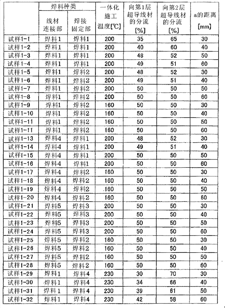
From above-mentioned table 2, find out, although any sample all carries out permissible shunting to the superconducting wire of layers 1 and 2, but as sample 1-1~1-4, at the scolder of the connecting portion of wire rod be welded and fixed the scolder place of section, when using scolder of the same race, the connecting length of wire rod is (apart from a) the longer the better.In addition, as sample 1-5~1-28, the scolder of the connecting portion of wire rod is different with the scolder kind that is welded and fixed section, and the connecting length of wire rod if the resistivity of the scolder of connecting portion in liquid nitrogen is lower than the section of being welded and fixed (just diminishes apart from interdependency a).Particularly, as sample 1-9~1-12,1-17~1-28, if construction temperature when integrated is no more than the fusing point of the scolder that the connecting portion at wire rod uses, the interdependency of connecting length further diminishes.Construction temperature when integrated in order to control like this, wish that the fusing point of the scolder that uses at the connecting portion connected with the wire rod A of wire rod B and superconducting wire 2 is higher than the fusing point of the scolder used in the above-mentioned section of being welded and fixed.
In addition, as sample 1-29~1-32, even the scolder of the connecting portion of wire rod is different with the scolder kind that is welded and fixed section, if but use the resistivity scolder high than the scolder that is welded and fixed section in liquid nitrogen in the scolder of the connecting portion of wire rod, the interdependency of connecting length just becomes greatly.
In addition, when considering the affecting of environment, wish to use lead-free solder, like this, as sample 1-21~1-24, preferably from lead-free solder, use scolder that the resistivity of scolder in liquid nitrogen of connecting portion is low than the scolder that is welded and fixed section or the scolder of the same kind of use in lead-free solder.
In addition, the resistance of the connecting portion of wire rod can be adjusted by " sectional area of the resistivity of scolder * solder thickness ÷ connecting portion ".As previously mentioned, preferably by the relation with the scolder fixed part, the scolder of selecting fusing point scolder higher and that resistivity is lower to use as the connecting portion at wire rod in eutectic solder, if but considered the impact for the heat of superconducting wire, scolder 1 geometric ratio scolder 5 would be more preferably.
In addition, the shape of the scolder that the wire rod A of the 1st superconducting wire 2 and wire rod B are used while engaging is preferably band shape, and the thinner manufacture of tape thickness now is just more difficult.
That is, limit the thickness of scolder kind (resistivity) and scolder at the connecting portion of wire rod, therefore, in the adjustment of the resistance of the connecting portion of wire rod, preferably adjust the connecting length a of the superconducting wire of above-mentioned connection use superconducting wire and the 1st layer.But if connecting length a is elongated, the section of being welded and fixed of current terminal part will become many so, from compactedness, considers not to be preferred situation.Preferably preferably connecting length is 50mm~100mm left and right.
Comparative example 1
Similarly to Example 1, after the 2nd superconducting wire of the 1st superconducting wire by the 1st layer and the 2nd layer spirally is wrapped on mould, different from embodiment 1, do not use to connect and use wire rod B, but use reticular zone and scolder to carry out the integrated of end, just obtain the sample of structure as shown in Figure 8.
About this sample, switch in liquid nitrogen, measured to the shunt ratio of the 1st superconducting wire and the 2nd superconducting wire, to the shunt ratio of the 1st superconducting wire for being less than 1%, shunt ratio to the 2nd superconducting wire is more than 99%, and electric current is hardly to the 1st superconducting wire shunting.
In addition, as a reference example, the 1st superconducting wire of the 1st layer and the 2nd superconducting wire of the 2nd layer are all used nonmagnetic substrate, spirally be wound around the face that makes superconducting layer and become table side (outside), carry out end integrated the same as comparative example 1, the just sample of acquisition structure as shown in Figure 7.
About this sample, in liquid nitrogen, switch on, measured to the shunt ratio of the 1st superconducting wire and the 2nd superconducting wire, to the shunt ratio of the 1st superconducting wire, be 50%, to the shunt ratio of the 2nd superconducting wire, be 50%, realized almost impartial shunting.
Similarly to Example 1, obtain structure as shown in Figure 1.Now, make length (with the connecting length that the is welded and fixed section) b that strips out of the 2nd superconducting wire, with the relation that strips out length (with the connecting length that is welded and fixed section) c be connected with wire rod B, various variations occur, just obtain 7 samples.In addition, the sample of b<c+10 (mm) obtains 1, and the sample of b=c, b>c+10 (mm), b>c+100 (mm) respectively obtains 2.In addition, beyond b now and the relation property of c, use the condition identical with sample 1-1~1-3 of embodiment 1.
About these samples, in liquid nitrogen, switch on, measured to the shunt ratio of the 1st superconducting wire and the 2nd superconducting wire, obtain result as described in Table 3.
Table 3
| a=50mm | Shunting to the 1st layer of superconducting wire | Shunting to the 2nd layer of superconducting wire | |
| Sample 2-1 | b<c+10 | 45% | 55% |
| Sample 2-2 | b=c | 48% | 52% |
| Sample 2-3 | b=c | 49% | 51% |
| Sample 2-4 | b>c+10 | 49% | 51% |
| Sample 2-5 | b>c+10 | 49% | 51% |
| Sample 2-6 | b>c+100 | 50% | 50% |
| Sample 2-7 | b>c+100 | 50% | 50% |
Find out from above-mentioned table 3, although any sample all carries out permissible shunting to the superconducting wire of layers 1 and 2, when b=c or b>c, especially shunt especially uniformly.
Symbol description
1,21... mould, 2,22... the 1st superconducting wire
2a, 3a, 4a, 6a, 7a, 8a, 22a, the 23a... substrate,
2b, 3b, 4b, 6b, 7b, 8b, 22b, the 23b... superconducting layer,
3,23... the 2nd superconducting wire, 5,9,15,17,19,24... scolder fixed part
6... the 3rd superconducting wire, 7... the 4th superconducting wire, 11... fixture, 12... reticular zone,
13... the 5th superconducting wire, 14... the 6th superconducting wire, 16, the non magnetic superconducting wire of 18....
Claims (11)
1. the current terminal structure of a superconductor,
Above-mentioned superconductor is that the superconducting wire that will be formed with superconducting layer on substrate is wound around more than 1 layer and the superconductor obtained on mould, directly be wrapped in the 1st layer of superconducting wire on above-mentioned mould with substrate-side become the outside, the superconducting layer side becomes inboard mode and is configured,
It is characterized in that the connecting opposite to each other with the part be connected with the face towards the outside of the superconducting layer of superconducting wire towards inboard face of the superconducting layer of the end of above-mentioned the 1st layer of superconducting wire.
2. the current terminal structure of superconductor according to claim 1, is characterized in that,
On above-mentioned the 1st layer of superconducting wire, with the superconducting layer side become the outside, substrate-side becomes inboard mode and is wound with the 2nd layer of superconducting wire,
Described current terminal structure possesses the section of being welded and fixed, and this section of being welded and fixed is used scolder to make the end of part that above-mentioned connection exposes with the superconducting layer of superconducting wire and above-mentioned the 2nd layer of superconducting wire integrated.
3. the current terminal structure of superconductor according to claim 2, is characterized in that,
The scolder that above-mentioned connection is used with the connecting portion of superconducting wire and above-mentioned the 1st layer of superconducting wire is less than or equal to the resistivity of the scolder that the above-mentioned section of being welded and fixed uses in the resistivity under liquid-nitrogen temperature.
4. the current terminal structure of superconductor according to claim 2, is characterized in that,
The fusing point of the scolder that the fusing point of the scolder that above-mentioned connection is used with the connecting portion of superconducting wire and above-mentioned the 1st layer of superconducting wire is used than the above-mentioned section of being welded and fixed is high.
5. the current terminal structure of superconductor according to claim 2, is characterized in that,
Above-mentioned connection with superconducting wire with the above-mentioned connecting length b that is welded and fixed section and above-mentioned the 2nd layer of superconducting wire meet the relation of b >=c with the above-mentioned connecting length c that is welded and fixed section.
6. the current terminal structure of a superconductor,
Above-mentioned superconductor is that the superconducting wire that will be formed with superconducting layer on substrate is wound around more than 4 layers and the superconductor obtained on mould, the odd-level superconducting wire with substrate-side become the outside, the superconducting layer side becomes inboard mode and is configured,
It is characterized in that the connecting opposite to each other with the part be connected with the face towards the outside of the superconducting layer of superconducting wire towards inboard face of the superconducting layer of the end of above-mentioned odd-level superconducting wire.
7. the current terminal structure of superconductor according to claim 6, is characterized in that,
On above-mentioned odd-level superconducting wire, with the superconducting layer side become the outside, substrate-side becomes inboard mode and is wound with above-mentioned odd number and adds one deck superconducting wire,
Described current terminal structure possesses the section of being welded and fixed, and the end that this section of being welded and fixed is used scolder to make part that above-mentioned connection exposes with the superconducting layer of superconducting wire and above-mentioned odd number add one deck superconducting wire is integrated.
8. the current terminal structure of superconductor according to claim 7, is characterized in that,
The scolder that above-mentioned connection is used with the connecting portion of superconducting wire and above-mentioned odd-level superconducting wire is less than or equal to the resistivity of the scolder that the above-mentioned section of being welded and fixed uses in the resistivity under liquid-nitrogen temperature.
9. the current terminal structure of superconductor according to claim 7, is characterized in that,
The fusing point of the scolder that the fusing point of the scolder that above-mentioned connection is used with the connecting portion of superconducting wire and above-mentioned odd-level superconducting wire is used than the above-mentioned section of being welded and fixed is high.
10. the current terminal structure of superconductor according to claim 7, is characterized in that,
Above-mentioned connection with superconducting wire add one deck superconducting wire with the above-mentioned connecting length b that is welded and fixed section and above-mentioned odd number meet the relation of b >=c with the above-mentioned connecting length c that is welded and fixed section.
11. a hyperconductive cable is characterized in that possessing:
The described current terminal structure of any one of claim 1~8.
Applications Claiming Priority (3)
| Application Number | Priority Date | Filing Date | Title |
|---|---|---|---|
| JP2009-109808 | 2009-04-28 | ||
| JP2009109808 | 2009-04-28 | ||
| PCT/JP2010/057611 WO2010126099A1 (en) | 2009-04-28 | 2010-04-28 | Current terminal structure of superconducting wire material and superconducting cable having this current terminal structure |
Publications (2)
| Publication Number | Publication Date |
|---|---|
| CN102396112A CN102396112A (en) | 2012-03-28 |
| CN102396112B true CN102396112B (en) | 2013-12-18 |
Family
ID=43032243
Family Applications (1)
| Application Number | Title | Priority Date | Filing Date |
|---|---|---|---|
| CN2010800163827A Active CN102396112B (en) | 2009-04-28 | 2010-04-28 | Current terminal structure of superconducting wire material and superconducting cable having this current terminal structure |
Country Status (4)
| Country | Link |
|---|---|
| US (1) | US8260388B2 (en) |
| JP (1) | JP5619731B2 (en) |
| CN (1) | CN102396112B (en) |
| WO (1) | WO2010126099A1 (en) |
Families Citing this family (7)
| Publication number | Priority date | Publication date | Assignee | Title |
|---|---|---|---|---|
| US9755329B2 (en) * | 2013-06-14 | 2017-09-05 | Advanced Conductor Technologies Llc | Superconducting cable connections and methods |
| JP6210537B2 (en) * | 2013-08-06 | 2017-10-11 | 古河電気工業株式会社 | Superconducting cable connection structure, superconducting cable, current terminal structure at the end of superconducting cable |
| FR3010847B1 (en) * | 2013-09-19 | 2017-12-29 | Nexans | JUNCTION OF SUPERCONDUCTING CABLES |
| JP6356048B2 (en) * | 2014-11-12 | 2018-07-11 | 古河電気工業株式会社 | Superconducting wire connection structure, superconducting cable, superconducting coil, and superconducting wire connection processing method |
| US9875826B2 (en) * | 2014-11-14 | 2018-01-23 | Novum Industria Llc | Field makeable cryostat/current connections for an HTS tape power cable |
| CN110692052A (en) * | 2017-06-02 | 2020-01-14 | 苹果公司 | Device, method and graphical user interface for presenting representations of media containers |
| CN107579356B (en) * | 2017-08-23 | 2019-03-19 | 国家电网公司 | A kind of welded type cable conductor connector and welding method with current balance function |
Family Cites Families (12)
| Publication number | Priority date | Publication date | Assignee | Title |
|---|---|---|---|---|
| EP1451832A1 (en) * | 2001-10-12 | 2004-09-01 | Southwire Company | Superconducting cable termination |
| JP4391066B2 (en) * | 2002-08-26 | 2009-12-24 | 古河電気工業株式会社 | Multi-layered superconducting conductor terminal structure and manufacturing method thereof |
| JP4399763B2 (en) * | 2003-02-28 | 2010-01-20 | 住友電気工業株式会社 | DC superconducting cable line |
| JP4191544B2 (en) * | 2003-06-19 | 2008-12-03 | 住友電気工業株式会社 | Superconducting cable joint structure |
| JP4182832B2 (en) * | 2003-08-18 | 2008-11-19 | 住友電気工業株式会社 | Superconducting plate connection method and connection part thereof |
| JP2005253204A (en) * | 2004-03-04 | 2005-09-15 | Sumitomo Electric Ind Ltd | Terminal structure of polyphase superconducting cable |
| JP4810268B2 (en) * | 2006-03-28 | 2011-11-09 | 株式会社東芝 | Superconducting wire connection method and superconducting wire |
| JP5192741B2 (en) * | 2006-07-20 | 2013-05-08 | 古河電気工業株式会社 | Superconducting conductor and superconducting cable with superconducting conductor |
| JP4845040B2 (en) * | 2007-03-20 | 2011-12-28 | 古河電気工業株式会社 | Thin film superconducting wire connection method and connection structure thereof |
| JP2009016253A (en) * | 2007-07-06 | 2009-01-22 | Sumitomo Electric Ind Ltd | Connection structure of superconducting wire rod as well as connecting method of superconductive apparatus and superconducting wire rod |
| JP5416924B2 (en) * | 2008-06-18 | 2014-02-12 | 株式会社東芝 | Superconducting wire and method for manufacturing the same |
| WO2011040381A1 (en) * | 2009-09-29 | 2011-04-07 | 古河電気工業株式会社 | Substrate for superconducting wiring, superconducting wiring and production method for same |
-
2010
- 2010-04-28 CN CN2010800163827A patent/CN102396112B/en active Active
- 2010-04-28 WO PCT/JP2010/057611 patent/WO2010126099A1/en active Application Filing
- 2010-04-28 JP JP2011511446A patent/JP5619731B2/en active Active
-
2011
- 2011-09-23 US US13/243,630 patent/US8260388B2/en active Active
Also Published As
| Publication number | Publication date |
|---|---|
| JPWO2010126099A1 (en) | 2012-11-01 |
| WO2010126099A1 (en) | 2010-11-04 |
| US20120015816A1 (en) | 2012-01-19 |
| JP5619731B2 (en) | 2014-11-05 |
| US8260388B2 (en) | 2012-09-04 |
| CN102396112A (en) | 2012-03-28 |
Similar Documents
| Publication | Publication Date | Title |
|---|---|---|
| CN102396112B (en) | Current terminal structure of superconducting wire material and superconducting cable having this current terminal structure | |
| KR101380921B1 (en) | Superconducting cables and methods of making the same | |
| JP4810268B2 (en) | Superconducting wire connection method and superconducting wire | |
| US7586717B2 (en) | Electrical device for current conditioning | |
| JP2018532262A (en) | High temperature superconducting coil with smart insulation, high temperature superconducting wire used therefor, and manufacturing method thereof | |
| US8034746B2 (en) | Method of manufacturing round wire using superconducting tape and round wire manufactured using the superconducting tape | |
| US20170125924A1 (en) | Generation of a Splice Between Superconductor Materials | |
| WO2015129272A1 (en) | Terminal structure for superconducting cable and method for manufacturing same | |
| JP5118990B2 (en) | Superconducting tape wire and defect repair method | |
| US9159897B2 (en) | Superconducting structure having linked band-segments which are each overlapped by directly sequential additional band-segments | |
| JP5115778B2 (en) | Superconducting cable | |
| JP6818578B2 (en) | Superconducting cable connection | |
| JP2006059811A (en) | Compound conductor with multi-core superconductive strand | |
| JP3018534B2 (en) | High temperature superconducting coil | |
| JP5604213B2 (en) | Superconducting equipment | |
| JP4391066B2 (en) | Multi-layered superconducting conductor terminal structure and manufacturing method thereof | |
| JP2004200178A (en) | Oxide superconductor and its manufacturing method | |
| JPH0498773A (en) | Superconducting cable connection section | |
| JP2002075078A (en) | Superconducting cable and method for analyzing electric-current distribution in superconducting cable | |
| JP3363164B2 (en) | Superconducting conductor | |
| JP5041414B2 (en) | Superconducting wire and superconducting conductor | |
| JP2008282566A (en) | Bismuth oxide superconducting element wire, bismuth oxide superconductor, superconducting coil, and manufacturing method of them | |
| JP3568745B2 (en) | Oxide superconducting cable | |
| WO2005096440A1 (en) | Process for the preparation of low contact resistance contact on a high transition temperature superconductors | |
| CN114464365A (en) | Composite superconducting tape, composite body, method for producing composite superconducting tape, method for connecting or transitioning joints |
Legal Events
| Date | Code | Title | Description |
|---|---|---|---|
| C06 | Publication | ||
| PB01 | Publication | ||
| C10 | Entry into substantive examination | ||
| SE01 | Entry into force of request for substantive examination | ||
| C14 | Grant of patent or utility model | ||
| GR01 | Patent grant | ||
| C41 | Transfer of patent application or patent right or utility model | ||
| TR01 | Transfer of patent right |
Effective date of registration: 20160708 Address after: Tokyo, Japan, Japan Patentee after: Furukawa Electric Co., Ltd. Address before: Tokyo, Japan Patentee before: Int Superconductivity Tech Center Patentee before: Furukawa Electric Co., Ltd. |