CN102219552B - Semiconductor material compounded with In2O3 arrow-shaped nanostructure on silicon wafer and its preparation method - Google Patents
Semiconductor material compounded with In2O3 arrow-shaped nanostructure on silicon wafer and its preparation method Download PDFInfo
- Publication number
- CN102219552B CN102219552B CN 201010150564 CN201010150564A CN102219552B CN 102219552 B CN102219552 B CN 102219552B CN 201010150564 CN201010150564 CN 201010150564 CN 201010150564 A CN201010150564 A CN 201010150564A CN 102219552 B CN102219552 B CN 102219552B
- Authority
- CN
- China
- Prior art keywords
- arrow
- silicon wafer
- shaped
- semiconductor material
- crystal
- Prior art date
- Legal status (The legal status is an assumption and is not a legal conclusion. Google has not performed a legal analysis and makes no representation as to the accuracy of the status listed.)
- Expired - Fee Related
Links
Images
Landscapes
- Silicon Compounds (AREA)
- Crystals, And After-Treatments Of Crystals (AREA)
Abstract
本发明公开了一种在硅片上复合In2O3箭状纳米结构的半导体材料及其制备方法,其材料包括衬底,该衬底采用硅片,其衬底表面生长有In2O3晶体;所述的In2O3晶体长度为5~15μm,顶端为多面体结构,底部为棒状结构,棒状结构具有四个面,并从顶端到底端逐渐变细,10~30个箭状纳米结构底部聚在一起形成一个花束状结构。其制备方法是以In颗粒作为原料,利用热蒸发方法生长得到In2O3箭状纳米结构。本发明具有大面积生长,成本低,重复性高等优点,可结合目前成熟的半导体硅集成电路工艺,适合于集成纳米光电子器件的发展。The invention discloses a semiconductor material compounded with In 2 O 3 arrow-shaped nanostructures on a silicon wafer and a preparation method thereof. The material includes a substrate, the substrate adopts a silicon wafer, and In 2 O 3 grows on the surface of the substrate Crystal; the length of the In 2 O 3 crystal is 5-15 μm, the top is a polyhedral structure, the bottom is a rod-shaped structure, the rod-shaped structure has four faces, and gradually becomes thinner from the top to the bottom, and 10-30 arrow-shaped nanostructures The bottoms come together to form a bouquet-like structure. The preparation method uses In particles as raw materials, and grows In 2 O 3 arrow-shaped nanostructures by thermal evaporation. The invention has the advantages of large-area growth, low cost, high repeatability, etc., can be combined with the current mature semiconductor silicon integrated circuit technology, and is suitable for the development of integrated nanometer optoelectronic devices.
Description
技术领域 technical field
本发明涉及光电子材料、半导体材料与器件技术领域,具体地说,本发明涉及在硅片上复合In2O3箭状纳米结构的半导体材料及其制备方法。The invention relates to the technical fields of optoelectronic materials, semiconductor materials and devices, in particular, the invention relates to a semiconductor material compounded with In 2 O 3 arrow-shaped nanostructures on a silicon chip and a preparation method thereof.
背景技术 Background technique
In2O3是一种宽带隙透明半导体材料,其直接带隙在3.55~3.75eV范围内,具有良好的导电性和较高的透光率。由于其独特的电学、化学和光学性质,In2O3在化学、生物传感、太阳能电池、光催化、执行器、光电子和平板显示等领域具有广泛的应用空间。In 2 O 3 is a wide bandgap transparent semiconductor material with a direct bandgap in the range of 3.55-3.75eV, good electrical conductivity and high light transmittance. Due to its unique electrical, chemical, and optical properties, In2O3 has a wide range of applications in the fields of chemistry, biosensing, solar cells, photocatalysis, actuators, optoelectronics, and flat panel displays.
近来,人们利用各种方法(溶液法,分子束外延,脉冲激光沉积,金属有机物化学气相沉积等)制备出了各种不同的In2O3纳米结构,例如纳米线,纳米带,纳米方块,八面体,纳米箭等,并对这些纳米结构的光电特性进行了研究。但是能应用于大规模生产的方法很少,且反应条件苛刻,生产成本高昂。本发明所提供的In2O3箭状纳米结构及其制备方法,克服现有技术的缺陷,实现了在硅片上制备大规模的In2O3纳米结构,且方法简单,对设备及制备条件要求不高,适合大规模生产。In2O3箭状纳米结构具有纳米级的尖端,底部是棒状结构,其独特的构造,使得它可用于高效的场发射材料,且可用于制作各种精密仪器的探头;也可结合目前成熟的半导体硅集成电路工艺,适合于集成纳米光电子器件的发展。Recently, various methods (solution method, molecular beam epitaxy, pulsed laser deposition, metal-organic chemical vapor deposition, etc.) octahedron, nano arrows, etc., and the photoelectric properties of these nanostructures were studied. However, there are few methods that can be applied to large-scale production, and the reaction conditions are harsh and the production cost is high. The In 2 O 3 arrow-shaped nanostructure and its preparation method provided by the present invention overcome the defects of the prior art and realize the preparation of large-scale In 2 O 3 nanostructures on silicon wafers, and the method is simple, and the equipment and preparation Conditions are not demanding, suitable for large-scale production. The In 2 O 3 arrow-shaped nanostructure has a nanoscale tip and a rod-like structure at the bottom. Its unique structure makes it suitable for high-efficiency field emission materials, and can be used to make probes for various precision instruments; it can also be combined with current mature The advanced semiconductor silicon integrated circuit technology is suitable for the development of integrated nano-optoelectronic devices.
发明内容 Contents of the invention
本发明的目的之一在于提供一种在硅片上复合In2O3箭状纳米结构的半导体材料,包括硅片衬底,和生长在所述衬底表面的In2O3晶体。其中,所述In2O3晶体为箭状纳米结构。One of the objectives of the present invention is to provide a semiconductor material compounded with In 2 O 3 arrow-shaped nanostructures on a silicon wafer, including a silicon wafer substrate and In 2 O 3 crystals grown on the surface of the substrate. Wherein, the In 2 O 3 crystal is an arrow-shaped nanostructure.
本发明提供的在硅片上复合In2O3箭状纳米结构的半导体材料,这种纳米结构具有很明显的周期性,所述的In2O3晶体长度为5~15μm,顶端为多面体结构,底部为棒状结构,棒状结构具有四个面,并从顶端到底端逐渐变细,10~30个箭状纳米结构底部聚在一起形成一个花束状结构。本发明提供的所述In2O3箭状纳米结构,在国际上尚属首次报道。The present invention provides a semiconductor material compounded with In 2 O 3 arrow-shaped nanostructures on a silicon wafer. This nanostructure has obvious periodicity. The length of the In 2 O 3 crystals is 5-15 μm, and the top is a polyhedral structure. , the bottom is a rod-shaped structure, the rod-shaped structure has four faces, and gradually becomes thinner from the top to the bottom, and 10 to 30 arrow-shaped nanostructures gather together at the bottom to form a bouquet-shaped structure. The In 2 O 3 arrow-shaped nanostructure provided by the present invention is reported for the first time in the world.
本发明的第二个目的在于提供在硅片上复合In2O3箭状纳米结构的半导体材料的制备方法,以解决现有In2O3纳米材料制备方法条件苛刻,成本高的问题,提供一种低成本,高重复性,适用于大规模工业生产的新方法。The second object of the present invention is to provide a method for preparing a semiconductor material compounding In 2 O 3 arrow-shaped nanostructures on a silicon chip, to solve the problems of harsh conditions and high cost of existing In 2 O 3 nano-material preparation methods, and provide A low-cost, highly reproducible, new method suitable for large-scale industrial production.
制备在硅片上复合In2O3箭状纳米结构的半导体材料的方法,包括如下步骤:A method for preparing a compound In2O3 arrow -shaped nanostructure semiconductor material on a silicon wafer, comprising the steps of:
a、将In颗粒作为源放到石英舟里,把清洗后的硅片盖在石英舟的上面,硅片与源的垂直距离为4~10mm;a. Put In particles as a source into a quartz boat, cover the cleaned silicon wafer on top of the quartz boat, and the vertical distance between the silicon wafer and the source is 4-10mm;
b、把石英舟放到预先加热至700~1000℃的水平放置的管式生长炉的中部;b. Put the quartz boat in the middle of the horizontal tubular growth furnace heated to 700-1000°C in advance;
c、通入惰性气体Ar作为载气,在大气压强下反应,得到产物。c. Feed in an inert gas Ar as a carrier gas, and react under atmospheric pressure to obtain a product.
其中,所述步骤a中所述In颗粒的纯度为99.999%。Wherein, the purity of the In particles in the step a is 99.999%.
其中,所述步骤c中所述通入的惰性气体Ar的流量为0.2~0.6L/min;所述在大气压强下的反应时间为120~360min。Wherein, the flow rate of the inert gas Ar introduced in the step c is 0.2-0.6 L/min; the reaction time under atmospheric pressure is 120-360 min.
其中,所述水平放置的管式生长炉是由两根半径不同的管组成的,大的氧化铝管长度为70~100cm,直径为6~10cm;小的石英管长度为50~80cm,直径为3~5cm。反应时,把小口径的管子插入大口径管子中,反应在小管中进行,并且载气是直接通入到小口径管子中。Wherein, the horizontal tube growth furnace is composed of two tubes with different radii. The large alumina tube is 70-100 cm in length and 6-10 cm in diameter; the small quartz tube is 50-80 cm in length and 6-10 cm in diameter. It is 3 ~ 5cm. During the reaction, a small-diameter tube is inserted into a large-diameter tube, and the reaction is carried out in the small-diameter tube, and the carrier gas is directly passed into the small-diameter tube.
制备在硅片上复合In2O3箭状纳米结构的半导体材料的方法,具体步骤包括如下:A method for preparing a compound In2O3 arrow-shaped nanostructured semiconductor material on a silicon wafer , the specific steps include the following:
a、把硅片清洗干净,然后切成几小片;a. Clean the silicon wafer and cut it into several small pieces;
b、将水平放置的管式生长炉以5℃/min的速率加热到700~1000℃;b. Heating the horizontal tubular growth furnace to 700-1000°C at a rate of 5°C/min;
c、将纯度99.999%的In颗粒作为源放到一个石英舟里,把一小片干净的硅片盖在石英舟的上面,作为衬底来收集反应生成物,硅片与源的垂直距离为4~10mm;c. Put In particles with a purity of 99.999% as a source into a quartz boat, and cover a small piece of clean silicon wafer on top of the quartz boat as a substrate to collect the reaction product. The vertical distance between the silicon wafer and the source is 4 ~10mm;
d、把石英舟放到预先加热好的水平管式炉的中部;d. Put the quartz boat in the middle of the preheated horizontal tube furnace;
e、通入流量为0.2~0.6L/min的惰性气体Ar作为载气,在大气压强下反应120~360min;e. The inert gas Ar with a flow rate of 0.2-0.6L/min is used as the carrier gas, and the reaction is carried out at atmospheric pressure for 120-360 minutes;
f、取出石英舟和硅片,在硅片上面长有一层淡黄色的物质。f. Take out the quartz boat and the silicon chip, and there is a layer of light yellow substance growing on the silicon chip.
本发明通过改变对热蒸发过程中一些参量,如气体流量,反应温度,硅片与源之间距离的控制,合成了In2O3箭状纳米结构。相对于以前合成的纳米结构,本发明的突出特点是:(1)所放硅片衬底位置不同。许多合成方法都把硅衬底放在气流的下流,与源在同一水平位置,而本发明则把硅片直接放在与源的垂直方向上的某一位置;(2)压力只需要是常压,降低了对设备的要求;(3)不需要引入任何催化剂;(4)对载气的要求不高,只需要Ar就可以,不需要加O2等另外的气体;(5)方法简单,成本低,重复性好,而且是大面积的生长。且本发明采用硅片作为衬底,将In2O3箭状纳米结构生长在硅衬底上,可结合目前成熟的半导体硅集成电路工艺,适合于集成纳米光电子器件的发展。The present invention synthesizes the arrow-shaped In 2 O 3 nanostructure by changing the control of some parameters in the thermal evaporation process, such as gas flow rate, reaction temperature, and the distance between the silicon chip and the source. Compared with the previously synthesized nanostructures, the outstanding features of the present invention are: (1) The positions of the placed silicon chip substrates are different. Many synthetic methods all place silicon substrate on the downstream of air-flow, and source is at the same horizontal position, and the present invention then directly places silicon chip on a certain position on the vertical direction with source; (2) pressure only needs to be normal (3) No need to introduce any catalyst; (4) The requirements for the carrier gas are not high, only Ar is needed, no need to add O2 and other gases; (5) The method is simple , low cost, good repeatability, and large area growth. Moreover, the present invention uses a silicon wafer as a substrate, and grows the In 2 O 3 arrow-shaped nanostructure on the silicon substrate, which can be combined with the current mature semiconductor silicon integrated circuit technology, and is suitable for the development of integrated nano-optoelectronic devices.
附图说明 Description of drawings
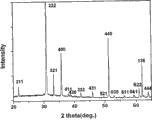
图1是箭状纳米结构的X射线衍射图Figure 1 is the X-ray diffraction pattern of the arrow-shaped nanostructure
图1显示所有的峰都是In2O3的峰,没有任何杂质峰存在。Figure 1 shows that all peaks are In 2 O 3 peaks without any impurity peaks.
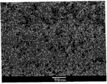
图2是大量箭状纳米结构的SEM图Figure 2 is a SEM image of a large number of arrow-shaped nanostructures
图2显示In2O3晶体长度为5~15μm,10~30个箭状纳米结构底部聚在一起形成一个花束状结构。Figure 2 shows that the In 2 O 3 crystal length is 5-15 μm, and 10-30 arrow-shaped nanostructures gather together at the bottom to form a bouquet-like structure.
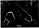
图3是箭状纳米结构的放大倍数的SEM图Figure 3 is a SEM image of the magnification of the arrow-shaped nanostructure
图3显示In2O3晶体顶端为多面体结构,底部为棒状结构,棒状结构具有四个面,并从顶端到底端逐渐变细。Figure 3 shows that the In 2 O 3 crystal has a polyhedral structure at the top and a rod-like structure at the bottom. The rod-like structure has four faces and gradually becomes thinner from the top to the bottom.
具体实施方式 Detailed ways
实施例1Example 1
制备在硅片上复合In2O3箭状纳米结构的半导体材料,具体步骤如下:To prepare semiconductor materials compounded with In 2 O 3 arrow-shaped nanostructures on a silicon wafer, the specific steps are as follows:
a、把硅片清洗干净,然后切成几小片;a. Clean the silicon wafer and cut it into several small pieces;
b、将水平放置的管式生长炉以5℃/min的速率加热到700℃;b. Heating the horizontal tubular growth furnace to 700°C at a rate of 5°C/min;
c、将In颗粒(纯度:99.999%)作为源放到一个石英舟里,把一小片干净的硅片盖在石英舟的上面,作为衬底来收集反应生成物,硅片与源的垂直距离为7mm;c. Put In particles (purity: 99.999%) as a source into a quartz boat, cover a small piece of clean silicon wafer on top of the quartz boat, and use it as a substrate to collect reaction products, the vertical distance between the silicon wafer and the source 7mm;
d、把石英舟放到预先加热好的水平管式炉的中部;d. Put the quartz boat in the middle of the preheated horizontal tube furnace;
e、通入流量为0.4L/min的惰性气体Ar作为载气,在大气压强下反应240min;e. The inert gas Ar with a flow rate of 0.4L/min is used as the carrier gas, and the reaction is carried out at atmospheric pressure for 240 minutes;
f、取出石英舟和硅片,在硅片上面长有一层淡黄色的物质,即制得所需材料。f. Take out the quartz boat and the silicon chip, and a layer of light yellow substance grows on the silicon chip, which means the required material is obtained.
检测所制得的材料,检测结果如图1、2、3所示。图1显示所有的峰都是In2O3的峰,没有任何杂质峰存在。图2显示In2O3晶体长度为5~15μm,10~30个箭状纳米结构底部聚在一起形成一个花束状结构。图3显示In2O3晶体顶端为多面体结构,底部为棒状结构,棒状结构具有四个面,并从顶端到底端逐渐变细。The prepared materials were tested, and the test results are shown in Figures 1, 2 and 3. Figure 1 shows that all peaks are In 2 O 3 peaks without any impurity peaks. Figure 2 shows that the In 2 O 3 crystal length is 5-15 μm, and 10-30 arrow-shaped nanostructures gather together at the bottom to form a bouquet-like structure. Figure 3 shows that the In 2 O 3 crystal has a polyhedral structure at the top and a rod-like structure at the bottom. The rod-like structure has four faces and gradually becomes thinner from the top to the bottom.
实施例2Example 2
制备在硅片上复合In2O3箭状纳米结构的半导体材料,具体步骤如下:To prepare semiconductor materials compounded with In 2 O 3 arrow-shaped nanostructures on a silicon wafer, the specific steps are as follows:
a、把硅片清洗干净,然后切成几小片;a. Clean the silicon wafer and cut it into several small pieces;
b、将水平放置的管式生长炉以5℃/min的速率加热到1000℃;b. Heating the horizontal tubular growth furnace to 1000°C at a rate of 5°C/min;
c、将In颗粒(纯度:99.999%)作为源放到一个石英舟里,把一小片干净的硅片盖在石英舟的上面,作为衬底来收集反应生成物,硅片与源的垂直距离为8mm;c. Put In particles (purity: 99.999%) as a source into a quartz boat, cover a small piece of clean silicon wafer on top of the quartz boat, and use it as a substrate to collect reaction products, the vertical distance between the silicon wafer and the source 8mm;
d、把石英舟放到预先加热好的水平管式炉的中部;d. Put the quartz boat in the middle of the preheated horizontal tube furnace;
e、通入流量为0.6L/min的惰性气体Ar作为载气,在大气压强下反应180min;e. The inert gas Ar with a flow rate of 0.6L/min was introduced as a carrier gas, and the reaction was carried out at atmospheric pressure for 180 minutes;
f、取出石英舟和硅片,在硅片上面长有一层淡黄色的物质,即制得所需材料。f. Take out the quartz boat and the silicon chip, and a layer of light yellow substance grows on the silicon chip, which means the required material is obtained.
检测所制得的材料,检测结果如图1、2、3所示。图1显示所有的峰都是In2O3的峰,没有任何杂质峰存在。图2显示In2O3晶体长度为5~15μm,10~30个箭状纳米结构底部聚在一起形成一个花束状结构。图3显示In2O3晶体顶端为多面体结构,底部为棒状结构,棒状结构具有四个面,并从顶端到底端逐渐变细。The prepared materials were tested, and the test results are shown in Figures 1, 2 and 3. Figure 1 shows that all peaks are In 2 O 3 peaks without any impurity peaks. Figure 2 shows that the In 2 O 3 crystal length is 5-15 μm, and 10-30 arrow-shaped nanostructures gather together at the bottom to form a bouquet-like structure. Figure 3 shows that the In 2 O 3 crystal has a polyhedral structure at the top and a rod-like structure at the bottom. The rod-like structure has four faces and gradually becomes thinner from the top to the bottom.
Claims (3)
Priority Applications (1)
| Application Number | Priority Date | Filing Date | Title |
|---|---|---|---|
| CN 201010150564 CN102219552B (en) | 2010-04-19 | 2010-04-19 | Semiconductor material compounded with In2O3 arrow-shaped nanostructure on silicon wafer and its preparation method |
Applications Claiming Priority (1)
| Application Number | Priority Date | Filing Date | Title |
|---|---|---|---|
| CN 201010150564 CN102219552B (en) | 2010-04-19 | 2010-04-19 | Semiconductor material compounded with In2O3 arrow-shaped nanostructure on silicon wafer and its preparation method |
Publications (2)
| Publication Number | Publication Date |
|---|---|
| CN102219552A CN102219552A (en) | 2011-10-19 |
| CN102219552B true CN102219552B (en) | 2012-12-19 |
Family
ID=44776289
Family Applications (1)
| Application Number | Title | Priority Date | Filing Date |
|---|---|---|---|
| CN 201010150564 Expired - Fee Related CN102219552B (en) | 2010-04-19 | 2010-04-19 | Semiconductor material compounded with In2O3 arrow-shaped nanostructure on silicon wafer and its preparation method |
Country Status (1)
| Country | Link |
|---|---|
| CN (1) | CN102219552B (en) |
Families Citing this family (2)
| Publication number | Priority date | Publication date | Assignee | Title |
|---|---|---|---|---|
| CN103332725B (en) * | 2013-06-02 | 2015-05-20 | 浙江理工大学 | Hierarchical and ordered In2O3 structure grown on the surface of TiO2 nanofibers and its preparation method |
| TWI537213B (en) * | 2014-09-15 | 2016-06-11 | 許國明 | Indium oxide nanorod and manufacturing method thereof |
-
2010
- 2010-04-19 CN CN 201010150564 patent/CN102219552B/en not_active Expired - Fee Related
Non-Patent Citations (1)
| Title |
|---|
| 李强.In2O3纳米材料的制备和表征及发光特性研究.《中国优秀硕士学位论文全文数据库工程科技I辑》.2009,(第3期),第12-21页. * |
Also Published As
| Publication number | Publication date |
|---|---|
| CN102219552A (en) | 2011-10-19 |
Similar Documents
| Publication | Publication Date | Title |
|---|---|---|
| CN101550531B (en) | Method for preparing silicon nano structures | |
| Li et al. | Effect of seed layer on structural properties of ZnO nanorod arrays grown by vapor-phase transport | |
| CN104674343B (en) | Large single crystal graphene and preparation method thereof | |
| CN107445488B (en) | Method for preparing large-area uniform monolayer transition metal chalcogenide | |
| CN105668555B (en) | A kind of method for preparing three-dimensional grapheme | |
| CN104341006A (en) | Three-dimensional MoS2@MWNTs nanostructure and its preparation method | |
| CN102476823A (en) | Preparation method of zinc oxide micro-nano array and zinc oxide micro-nano array | |
| Kumar et al. | Synthesis of ZnO nanostructures | |
| Shen et al. | Morphology-controlled synthesis of ZnO nanostructures by a simple round-to-round metal vapor deposition route | |
| CN105481002A (en) | Method for Self-Catalytic Growth of Large Size β-Ga2O3 Micron Wires | |
| CN102219552B (en) | Semiconductor material compounded with In2O3 arrow-shaped nanostructure on silicon wafer and its preparation method | |
| CN103523818B (en) | A preparation method of highly oriented ZnO nanocone array structure material | |
| CN102211949B (en) | Semiconductor material and preparation method thereof compounding In2O3 multi-angle layered tower-like nanostructure on silicon wafer | |
| CN105347345A (en) | Silicon micro-nano structure preparing method | |
| CN101851114B (en) | A kind of semiconductor material and preparation method thereof compounding In2O3 tentacle-like nanostructure on silicon wafer | |
| CN102219553B (en) | Semiconductor material compounding In2O3 tower nanostructure on silicon wafer and its preparation method | |
| CN102212878B (en) | A kind of preparation method of needle-shaped and mushroom-shaped Bi2O3 nanomaterials | |
| CN106276922A (en) | A kind of intersecting vertical SiO2 nanorod and its preparation method | |
| CN101875565B (en) | A kind of semiconductor material and preparation method thereof compounded on silicon chip In2O3 flower-like nanostructure | |
| Nam et al. | Rutile structured SnO2 nanowires synthesized with metal catalyst by thermal evaporation method | |
| CN101693528B (en) | Method for growing ZnSe monocrystal nanowire | |
| CN102211948A (en) | Semiconductor material compounded with In2O3 layered rod-like nanostructure on silicon wafer and its preparation method | |
| CN101570892B (en) | Au-ZnO two-dimensional photon crystal structure and preparation method thereof | |
| Filippo et al. | Fabrication of α-TeO2 smooth and beaded microwires by thermal evaporation method | |
| CN101311386B (en) | A kind of preparation method of single crystal zinc sulfide nanowire |
Legal Events
| Date | Code | Title | Description |
|---|---|---|---|
| C06 | Publication | ||
| PB01 | Publication | ||
| C10 | Entry into substantive examination | ||
| SE01 | Entry into force of request for substantive examination | ||
| C14 | Grant of patent or utility model | ||
| GR01 | Patent grant | ||
| CF01 | Termination of patent right due to non-payment of annual fee |
Granted publication date: 20121219 Termination date: 20150419 |
|
| EXPY | Termination of patent right or utility model |