CN102200687A - Imprint apparatus and method of manufacturing an article - Google Patents
Imprint apparatus and method of manufacturing an article Download PDFInfo
- Publication number
- CN102200687A CN102200687A CN2011100711620A CN201110071162A CN102200687A CN 102200687 A CN102200687 A CN 102200687A CN 2011100711620 A CN2011100711620 A CN 2011100711620A CN 201110071162 A CN201110071162 A CN 201110071162A CN 102200687 A CN102200687 A CN 102200687A
- Authority
- CN
- China
- Prior art keywords
- resin
- mould
- gas
- pattern
- porous part
- Prior art date
- Legal status (The legal status is an assumption and is not a legal conclusion. Google has not performed a legal analysis and makes no representation as to the accuracy of the status listed.)
- Granted
Links
Images


Classifications
-
- B—PERFORMING OPERATIONS; TRANSPORTING
- B29—WORKING OF PLASTICS; WORKING OF SUBSTANCES IN A PLASTIC STATE IN GENERAL
- B29C—SHAPING OR JOINING OF PLASTICS; SHAPING OF MATERIAL IN A PLASTIC STATE, NOT OTHERWISE PROVIDED FOR; AFTER-TREATMENT OF THE SHAPED PRODUCTS, e.g. REPAIRING
- B29C35/00—Heating, cooling or curing, e.g. crosslinking or vulcanising; Apparatus therefor
- B29C35/02—Heating or curing, e.g. crosslinking or vulcanizing during moulding, e.g. in a mould
- B29C35/0227—Heating or curing, e.g. crosslinking or vulcanizing during moulding, e.g. in a mould using pressure vessels, e.g. autoclaves, vulcanising pans
- B29C35/0233—Heating or curing, e.g. crosslinking or vulcanizing during moulding, e.g. in a mould using pressure vessels, e.g. autoclaves, vulcanising pans the curing continuing after removal from the mould
-
- G—PHYSICS
- G03—PHOTOGRAPHY; CINEMATOGRAPHY; ANALOGOUS TECHNIQUES USING WAVES OTHER THAN OPTICAL WAVES; ELECTROGRAPHY; HOLOGRAPHY
- G03F—PHOTOMECHANICAL PRODUCTION OF TEXTURED OR PATTERNED SURFACES, e.g. FOR PRINTING, FOR PROCESSING OF SEMICONDUCTOR DEVICES; MATERIALS THEREFOR; ORIGINALS THEREFOR; APPARATUS SPECIALLY ADAPTED THEREFOR
- G03F7/00—Photomechanical, e.g. photolithographic, production of textured or patterned surfaces, e.g. printing surfaces; Materials therefor, e.g. comprising photoresists; Apparatus specially adapted therefor
- G03F7/0002—Lithographic processes using patterning methods other than those involving the exposure to radiation, e.g. by stamping
-
- B—PERFORMING OPERATIONS; TRANSPORTING
- B29—WORKING OF PLASTICS; WORKING OF SUBSTANCES IN A PLASTIC STATE IN GENERAL
- B29C—SHAPING OR JOINING OF PLASTICS; SHAPING OF MATERIAL IN A PLASTIC STATE, NOT OTHERWISE PROVIDED FOR; AFTER-TREATMENT OF THE SHAPED PRODUCTS, e.g. REPAIRING
- B29C33/00—Moulds or cores; Details thereof or accessories therefor
- B29C33/38—Moulds or cores; Details thereof or accessories therefor characterised by the material or the manufacturing process
- B29C33/3842—Manufacturing moulds, e.g. shaping the mould surface by machining
- B29C33/3857—Manufacturing moulds, e.g. shaping the mould surface by machining by making impressions of one or more parts of models, e.g. shaped articles and including possible subsequent assembly of the parts
- B29C33/3878—Manufacturing moulds, e.g. shaping the mould surface by machining by making impressions of one or more parts of models, e.g. shaped articles and including possible subsequent assembly of the parts used as masters for making successive impressions
- B29C33/3885—Manufacturing moulds, e.g. shaping the mould surface by machining by making impressions of one or more parts of models, e.g. shaped articles and including possible subsequent assembly of the parts used as masters for making successive impressions the mould parts being co-operating impressions
-
- B—PERFORMING OPERATIONS; TRANSPORTING
- B29—WORKING OF PLASTICS; WORKING OF SUBSTANCES IN A PLASTIC STATE IN GENERAL
- B29C—SHAPING OR JOINING OF PLASTICS; SHAPING OF MATERIAL IN A PLASTIC STATE, NOT OTHERWISE PROVIDED FOR; AFTER-TREATMENT OF THE SHAPED PRODUCTS, e.g. REPAIRING
- B29C59/00—Surface shaping of articles, e.g. embossing; Apparatus therefor
- B29C59/02—Surface shaping of articles, e.g. embossing; Apparatus therefor by mechanical means, e.g. pressing
-
- B—PERFORMING OPERATIONS; TRANSPORTING
- B82—NANOTECHNOLOGY
- B82Y—SPECIFIC USES OR APPLICATIONS OF NANOSTRUCTURES; MEASUREMENT OR ANALYSIS OF NANOSTRUCTURES; MANUFACTURE OR TREATMENT OF NANOSTRUCTURES
- B82Y10/00—Nanotechnology for information processing, storage or transmission, e.g. quantum computing or single electron logic
-
- B—PERFORMING OPERATIONS; TRANSPORTING
- B82—NANOTECHNOLOGY
- B82Y—SPECIFIC USES OR APPLICATIONS OF NANOSTRUCTURES; MEASUREMENT OR ANALYSIS OF NANOSTRUCTURES; MANUFACTURE OR TREATMENT OF NANOSTRUCTURES
- B82Y40/00—Manufacture or treatment of nanostructures
-
- H—ELECTRICITY
- H01—ELECTRIC ELEMENTS
- H01L—SEMICONDUCTOR DEVICES NOT COVERED BY CLASS H10
- H01L21/00—Processes or apparatus adapted for the manufacture or treatment of semiconductor or solid state devices or of parts thereof
- H01L21/02—Manufacture or treatment of semiconductor devices or of parts thereof
- H01L21/027—Making masks on semiconductor bodies for further photolithographic processing not provided for in group H01L21/18 or H01L21/34
- H01L21/0271—Making masks on semiconductor bodies for further photolithographic processing not provided for in group H01L21/18 or H01L21/34 comprising organic layers
- H01L21/0273—Making masks on semiconductor bodies for further photolithographic processing not provided for in group H01L21/18 or H01L21/34 comprising organic layers characterised by the treatment of photoresist layers
- H01L21/0274—Photolithographic processes
Abstract
An imprint apparatus which cures a resin dispensed on a substrate while the resin and a pattern surface of a mold are in contact with each other, comprises a supply portion configured to supply a gas, used to accelerate filling of a concave portion of the pattern surface of the mold with the resin, to a space which the pattern surface of the mold faces, and a controller configured to control the supply portion to supply the gas to the space before the resin and the pattern surface of the mold are brought into contact with each other, wherein the supply portion is configured to supply the gas to the space via a porous portion formed in at least part of the mold.
Description
Technical field
The present invention relates to Embosser and use this Embosser to make the method for article.
Background technology
Stamping technique just as intention be used for magnetic storage medium and semiconductor devices batch process one type photoetching technique and come into operation.The stamping technique that forms the pattern of nanometer scale is called as nanometer embossing.Stamping technique relate to be crushed on the resin, form figuratum mould (master) on it, wherein said resin is coated on the substrate such as silicon wafer (wafer) or glass plate.Cured resin under this state, thus with pattern transfer to substrate.
Traditional method for stamping causes following problem, and promptly the sunk part with the pattern that forms on the resin fill mold will spend the long time, and if carried out curing process then defective occurs before the sunk part of pattern is by the resin complete filling.Traditional method for stamping also causes following problem, promptly needs bigger power that mould is separated with resin or substrate after resin solidification, and this causes transferring to the defective in the pattern on the substrate.
Summary of the invention
The invention provides a kind of favourable technology to improve handling capacity and/or the yield rate that impression is handled in the layout that suppresses Embosser complicated.
A first aspect of the present invention provides a kind of Embosser, resin and the patterned surfaces of mould of described equipment on being coated on substrate makes described resin solidification when contacting with each other, described equipment comprises: supply section, be configured to the patterned surfaces of described mould towards the space supply gas, described gas is used to quicken to fill with described resin the sunk part of the patterned surfaces of described mould; And controller, be configured to control described supply section so as before the patterned surfaces that makes described resin and described mould to contact with each other to described space supply gas, wherein said supply section is configured to come to described space supply gas via the porous part that forms at least a portion of described mould.
A second aspect of the present invention provides a kind of Embosser, resin and the mould of described equipment on being coated on substrate makes described resin solidification when contacting with each other, described mould comprises porous part, and described Embosser comprises: chuck (chuck) is configured to keep described mould; And pumping unit, be configured to from the gas bleeding of described porous part by suction, make via of sunk part by the suction gas bleeding of described porous part, so that acceleration is filled described sunk part with described resin from the pattern that the pattern part of the described mould that contact with described resin, forms.
A third aspect of the present invention provides a kind of method of making article, and described method comprises the steps: to use the Embosser that limits as a first aspect of the present invention or second aspect that the pattern of resin is formed on the substrate; And handle on it and to form figuratum substrate.
From becoming clear below with reference to the more feature of the present invention the description of the exemplary embodiment of accompanying drawing.
Description of drawings
Figure 1A and Figure 1B are the figure that schematically shows according to the layout of the Embosser of the embodiment of the invention;
Fig. 2 is the figure that the illustrative arrangement of mould is shown;
Fig. 3 is the figure of the sunk part of the pattern that forms in the pattern part that schematically shows with the resin fill mold;
Fig. 4 A~4F is the figure that schematically shows according to the structure of the mould of first embodiment of the invention;
Fig. 5 A~5D is the figure that schematically shows according to the structure of the mould of second embodiment of the invention; And
Fig. 6 is the sequence chart that illustrates according to the operation of the Embosser of second embodiment of the invention.
Embodiment
Describe the preferred embodiments of the present invention below with reference to the accompanying drawings in detail.
[first embodiment]
To Embosser 100 according to first embodiment of the invention be described with reference to Figure 1A.At the patterned surfaces PS of mould 2 and the resin supplying energy of Embosser 100 when resin contacts, solidify this resin thus to coating on the substrate such as wafer or glass substrate 1.Therefore, will be at the pattern transfer that forms on the patterned surfaces PS of mould 2 pattern as resin to the substrate 1.Being used for the energy of cured resin typically is light (for example, ultraviolet light) or heat.Embosser 100 can comprise detent mechanism 12 of for example substrate 1 being located and the imprint head 3 with the chuck 14 that keeps mould 2.Embosser 100 can also comprise the controller CNT that controls coining manipulation in addition, make mould 2 via resin and substrate 1 contact or make driving mechanism (not shown) that mould 2 separates with substrate 1, by to the resin supplying energy and the solidified cell (not shown) of cured resin and with resin-coated coating mechanism to substrate 1.Driving mechanism can be configured to for example by driving imprint head 3 mould 2 is pressed on the substrate 1 via resin.In another embodiment, driving mechanism is built in the detent mechanism 12, and driving substrate 1 is pressed in state on the substrate 1 so that form mould 2 wherein via resin.Embosser 100 also comprises the supply section 16 to mould 2 supply gas.Scope (scope) 4 can be placed on the imprint head 3.Observe mark on scope 4 optics, detect their relative position thus in mark that forms on the mould 2 and formation on substrate 1.Detent mechanism 12 is located substrate 1 based on the relative position that is detected by scope 4.
Fig. 2 illustrates the illustrative arrangement of mould 2.Using the light such as ultraviolet light to come in the layout of cured resin, mould 2 is made by the light transmissive material such as quartz, and can be by falling to penetrating illumination (epi-illumination) via mould 2 rayed resin.Mould 2 can have following shape, and the lobed pattern part 5 of this shape, this pattern part 5 have the figuratum patterned surfaces PS of formation on it.Mould 2 contacted with the projected area that is adjacent to the target projected area on the substrate 1 when this had prevented mould 2 is pressed in target projection (shot) zone via resin on.
The pattern part 5 of the schematically illustrated mould 2 of Fig. 3 is pressed in the patterned surfaces PS and resin 7 state of contact that are coated on the substrate 1 of state on the substrate 1 or mould 2 via resin 7.The pattern that forms on the patterned surfaces PS in pattern part 5 comprises sunk part 6.In other words, pattern comprises sunk part 6 and bossing.When the pattern part 5 of mould 2 is pressed on the resin 7 that is coated on the substrate 1, by capillarity by the sunk part 6 of resin 7 filling patterns.Note that at pattern part 5 with before resin 7 contacts, gas is present in the sunk part 6.In general stamping technique, the gas that is present in the sunk part 6 is dissolved in the resin, uses resin complete filling sunk part 6 thus.For this reason, can use with the layout that dissolves in gas (for example, having low-molecular-weight hydrogen or helium) the covering imprint head 3 in the resin.Yet, so that when realizing that this arranges, also mobile coverture must be set so that for example replace the mechanism of mould 2, and this may make the complicated layoutization of Embosser 100 when the coverture (cover) that surrounds imprint head 3 is set.In addition, obducent installation may limit the degree of freedom that other device is installed.
Therefore, in the present embodiment, mould 2 is equipped with the porous part such as porous layer, so that gas is fed to pattern part 5 via porous part from Embosser 100.Porous part can be made by for example transparent material (such as the celelular silica material).Can be by forming celelular silica with several thickness coating member and heating and removal polymeric materials to the hundreds of micron with the mixed solution that wherein is dispersed with silica material and the polymeric material such as polystyrene particle.This method can obtain wherein for example to arrange regularly or brokenly the porous structure of several nanometers to the cavity of tens nanometer scale.Embosser 100 comprises the supply section 16 to the porous part supply gas of mould 2, shown in Figure 1A.Supply section 16 can comprise for example gas feed lines, gas supply source and pilot-gas supply and the valve that stops.
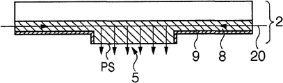
Some embodiment of mould 2 with the porous part such as porous layer will be described with reference to figure 4A~4D.In the shown example of Fig. 4 A, mould 2 has the porous part of arranging around pattern part 58, and from being arranged on supply section 16 (referring to Figure 1A) on the imprint head 3 to porous part 8 supply gas 20.Porous part 8 can be arranged in whole circumference and surround pattern part 5 everywhere.In the shown example of Fig. 4 B, partly cover porous part 8 so that the zone of gas is discharged in restriction from mould 2 with atresia parts 9.Atresia parts 9 are the parts of not allowing that gas passes through or gas passes through amount is littler than porous part 8.In Fig. 4 A and the shown layout of Fig. 4 B, can comprise or can not comprise the time period that mould 2 contacts with resin from the time period that porous part 8 is discharged gases.In Fig. 4 A and the shown example of Fig. 4 B, controller CNT control supply section 16 in case before the patterned surfaces PS that makes resin and mould 2 contacts with each other to patterned surfaces PS towards the space supply gas.
In the shown example of Fig. 4 C, pattern part 5 is formed by porous part 8, therefore also discharges gas from pattern part 5.Layout in the shown example of Fig. 4 C not only have to pattern part 5 towards the function of space (this space can also be expressed as the outside of pattern part 5 or the space of downside) supply gas, and have the function of removal attached to any foreign matter on the pattern part 5.In the shown layout of Fig. 4 C, pattern part 5 has low relatively intensity, therefore can use lid (capping) layer 10 that is formed by the atresia parts partly to cover porous part 8, so that form pattern part 5 in cap rock 10, shown in Fig. 4 D.The known low-molecular-weight gas that has such as hydrogen and helium generally passes through for example rubber and glass.Therefore, the SiO that for example has about tens nano thickness is set
xLayer (for example, SiO
2Layer) making as cap rock 10 can be not only by gas but also increase pattern intensity.In Fig. 4 C and the shown example of Fig. 4 D, controller CNT control supply section 16 so as during at least a portion of mould 2 and time period before resin contacts from porous part 8 discharge gases, and when mould 2 is pressed on the resin, during the time period of resin solidification, do not discharging gas.As in cap rock 10, forming substituting of pattern part 5, can form pattern part 5 by in porous part 8, forming pattern and covering this pattern with cap rock 10.In this case, cap rock 10 is formed the sufficiently little thickness of width that has than the sunk part 6 of the pattern that forms in porous part 8.
Fig. 4 E and Fig. 4 F illustrate the supply section 16 to porous part 8 supply gas of mould 2.According to present embodiment, by supply section 16 receiver gases from be arranged on Embosser 100 being set for mould 2 and discharging the porous part 8 of this gas, can be to the supply gas partly of the space between the pattern part 5 of each projected area on the substrate 1 and mould 2.This layout has been eliminated the obducent needs that are provided for surrounding imprint head 3, and therefore the size of Embosser 100 is dwindled.In addition, this layout can by discharge from porous part 8 gas that dissolves in the resin and the patterned surfaces PS in pattern part 5 towards the space supply this gas and patterned surfaces PS in pattern part 5 when contact with resin acceleration with resin filling sunk part 6.This makes and can improve the handling capacity that impression is handled.In addition, by quickening to fill sunk part 6, can reduce owing to not exclusively fill the pattern transfer inefficacy that sunk part 6 causes with resin, so that improve yield rate with resin.
[second embodiment]
Figure 1B illustrate Embosser 100 according to second embodiment of the invention ' illustrative arrangement.With the identical element of representing according to the identical Reference numeral of the element of the Embosser 100 of first embodiment among Figure 1B.According to the Embosser 100 of second embodiment ' the have layout that wherein replaces according to the supply section 16 in the Embosser 100 of first embodiment with Gas controller 18.Though mould 2 can have with first embodiment in similar arrangements, its preferably covers with atresia parts 9 in the part except that pattern part 5.Fig. 5 A illustrates an example of the mould 2 that can be used among second embodiment.Gas controller 18 comprises pumping unit, this pumping unit when the pattern part 5 of mould 2 is pressed on the resin 7 via the porous part 8 of the pattern part 5 that forms mould 2 by the gas in the sunk part 6 of extracting pattern out.Therefore, fill sunk part 6 more deeply, apace, schematically show as Fig. 5 B with resin 7.Gas controller 18 can also comprise the supply section to porous part 8 supply gas, thereby discharges gas from porous part 8.
Porous member has ratio as there not being the SiO of porous structure
2Low intensity.Therefore, such as SiO
xLayer (for example, SiO
2Layer) and so on thin cap rock (atresia parts) 10 can be stacked on the surface of porous part 8, and pattern part 5 can be formed on the cap rock 10, shown in Fig. 5 C and Fig. 5 D.When adopting SiO
xLayer is during as cap rock 10, with SiO
xAfter layer formed approach the same with about tens nanometers, gas can pass through SiO
xLayer.In this case, cap rock 10 and porous part 8 both as the parts that gas is passed through.In the shown example of Fig. 5 D, in pattern part 5, cap rock 10 can have the first 21 corresponding with sunk part 6 and with part (bossing) corresponding second portion 22 except that sunk part 6.First 21 is thinner than second portion 22, therefore with compare by second portion 22, gas more may pass through first 21.Therefore, and compare by second portion 22, can be by first 21 more easily from bottom gas bleeding of sunk part 6 by suction.As a result, effectively by extracting the gas in the sunk part 6 out.As in cap rock 10, forming substituting of pattern part 5, can form pattern part 5 by in porous part 8, forming pattern and covering this pattern with cap rock 10.In this case, cap rock 10 is formed the sufficiently little thickness of width that has than the sunk part 6 of the pattern that forms in porous part 8.
After filling sunk part 6, can come cured resin 7 by for example using the rayed resin 7 such as ultraviolet light with resin 7.Thereafter, mould 2 separates with the resin 7 or the substrate 1 that solidify.At this moment wait, power is used for the resin 7 that solidifies is pulled out sunk part 6, and therefore the resin 7 that solidifies may be damaged or peel off substrate 1.In order to prevent this, preferably from Gas controller 18 to porous part 8 supply gas so that it is supplied in the sunk part 6, help mould 2 to separate thus with resin 7.This makes and can make the pattern part 5 of resin 7 and mould 2 separated from one another with more weak power, therefore is reduced in the possibility that occurs defective when separating in the pattern of resin.Note that as above-described can be used as by the gas of porous part 8 will be to the gas of porous part 8 supplies.
Will with reference to figure 6 illustration Embossers 100 ' in coining manipulation.Controller CNT controls following sequence.Left side among Fig. 6 illustrates the sequence of coining manipulation, and the right side among Fig. 6 illustrates the operation of Gas controller 18.Load or impression (pattern transfer that comprises resin-coated, mold pressing and resin solidification) finishes (6-A-1) afterwards to previous projected area at new substrate, with resin-coated to the projected area of next wanting pattern transferring on it (6-A-2).Note that normally used resin has so high volatility and make that it evaporated when it is applied on the whole surface of substrate before mould 2 is pressed.In order to prevent this, practice is only to be close to before the transfer printing resin-coated to the projected area of next wanting pattern transferring on it usually.If resin has enough low volatility, then can be pressed on each projected area mould and resin solidification resin-coated the execution after to the whole surface of substrate.
Finish during driving substrate 1 makes that next projected area is positioned in random time section below the imprint head 3 loading or be impressed into previous projected area from substrate, that is to say, before the patterned surfaces PS that makes resin and mould 2 contacts with each other, can be by porous part 8 supply gas of Gas controller 18 to mould 2.Therefore, can discharge gas from the porous part 8 of mould 2, and can remove attached to any foreign matter on the pattern part 5.Note that then foreign matter may be fallen on the substrate 1 if discharge gas from porous part 8 in below substrate 1 is present in imprint head 3.In order to prevent this, Gas controller 18 can be operated so that unload carried base board 1 in for example position below imprint head 3 and discharge gases from porous part 8 during with the time period that is used for resin-coated time period or loading (or replacement) substrate 1.
Drive the substrate 1 that is coated with resin on it by detent mechanism 12, the projected area that makes pattern will be transferred on it is placed on imprint head 3 following (6-A-3).At this moment wait, by Gas controller 18 to porous part 8 supply gas.Therefore, gas is from porous part 8 discharges and to the supply of the space between imprint head 3 and substrate 1 (6-B-2).Imprint head 3 descended or make the operation that substrate 1 rises (that is the operation that the patterned surfaces PS of mould 2 is contacted with resin) begin (6-A-4) thereafter.In case the patterned surfaces PS of mould 2 contacts with each other with the resin that is coated on the substrate 1, just begin sunk part (6-A-5) with resin filling pattern part 5.Before filling beginning, stop, and when filling beginning, begin (6-B-3) via the gas pumping of porous part 8 from porous part 8 by Gas controller 18 by the gas supply (that is, discharging gases) of Gas controller 18 to porous part 8.In short time period, use the sunk part of resin filling pattern part 5 by intake-gas.After finishing filling, by the gas pumping end (6-B-4) of Gas controller 18 via porous part 8.Finish to fill (6-A-6) afterwards, by for example with the method for rayed resin solidify it (6-A-7).Mould 2 separates (6-A-8) with substrate 1.At this moment wait, by the gas supply (that is, discharging gas from mould) of Gas controller 18 execution to porous part 8, therefore quickening mould 2 separates (6-B-5) with substrate 1.With after substrate 1 separates end, finish (6-B-6) to the gas supply (that is, discharging gas) of porous part 8 at mould 2 from mould by Gas controller 18.Note that when for example interferometer is used as measurement mechanism,, therefore must carry out the gas discharge of minimum necessary amounts because the refractive index of air error may occur with difference between the refractive index of the gas of Gas controller 18 supplies measured value.After the impression processing to current projected area in the above described manner finished, the impression of carrying out on the next projected area was handled (6-A-9).
As mentioned above, by via sunk part 6 by the suction gas bleedings of porous part 8, can quicken to fill sunk part 6 with resin from the pattern part 5 of mould 2.In addition, by to sunk part 6 supply gas so that make mould 2 and the resin isolation of solidifying, can promote to separate, therefore reduce the defective that in the pattern of the resin that solidifies, may occur.In addition, by discharging gas, can remove any foreign matter from pattern part 5 to porous part 8 supply gas of mould 2 and from pattern part 5.This makes and can improve the handling capacity that impression handles and/or reduce owing to not exclusively fill the pattern transfer that sunk part 6 causes with resin and lost efficacy so that the raising yield rate.
[making the method for article]
A kind of method of making article comprises uses above-mentioned Embosser that pattern transfer (formation) is transferred to the step of the substrate on it to step and processing (for example, etching) pattern on the substrate (for example, wafer, glass plate or membranaceous substrate).The article of making can comprise the device such as semiconductor device and liquid crystal display device.
Though reference example embodiment has described the present invention, should be appreciated that to the invention is not restricted to disclosed exemplary embodiment.Thereby the scope of following claim will be given the wideest explanation comprises all such modifications, equivalent configurations and function.
Claims (7)
1. Embosser, the described equipment resin and patterned surfaces of mould on being coated on substrate makes described resin solidification when contacting with each other, and described equipment comprises:
Supply section, be configured to the patterned surfaces of described mould towards the space supply gas, described gas is used to quicken to fill with described resin the sunk part of the patterned surfaces of described mould; And
Controller, be configured to control described supply section in case before the patterned surfaces that makes described resin and described mould contacts with each other to described space supply gas,
Wherein said supply section is configured to come to described space supply gas via the porous part that forms at least a portion of described mould.
2. equipment according to claim 1, wherein
Described mould comprises pattern part, and described pattern part comprises patterned surfaces, and described pattern part is formed by described porous part, and
Described controller is controlled described supply section so that stopping to described porous part supply gas during the time period of described resin solidification when the patterned surfaces that makes described resin and described mould contacts with each other.
3. equipment according to claim 1, wherein
Described mould comprises cap rock, and described cap rock is made by the non-porous parts that part covers described porous part, is furnished with pattern part in described cap rock, and described cap rock has and be small enough to thickness that gas is passed through, and
Described supply section is stopping during the time period of described resin solidification to described porous part supply gas when being pressed in described mould on the described resin.
4. equipment according to claim 1, wherein said controller control described supply section in case from described supply section to described mould supply gas, make gas discharge, so that with the resin isolation of described mould and curing from the described porous part of described mould.
5. Embosser, described Embosser resin and mould on being coated on substrate makes described resin solidification when contacting with each other,
Described mould comprises porous part, and
Described Embosser comprises:
Chuck is configured to keep described mould; And
Pumping unit, be configured to from the gas bleeding of described porous part by suction, make via the gas bleeding by suction from the sunk part of the pattern that the pattern part of the described mould that contact with described resin, forms of described porous part, so that acceleration is filled described sunk part with described resin.
6. equipment according to claim 5 also comprises
Supply section is configured to the porous part supply gas to described mould, makes gas discharge from described porous part, so that quicken the resin isolation of described mould and curing.
7. method of making article, described method comprises the steps:
The Embosser that limits in use any one claim in claim 1~6 is formed on the pattern of resin on the substrate; And
Handle and form figuratum substrate on it.
Applications Claiming Priority (2)
| Application Number | Priority Date | Filing Date | Title |
|---|---|---|---|
| JP2010-068916 | 2010-03-24 | ||
| JP2010068916A JP5618588B2 (en) | 2010-03-24 | 2010-03-24 | Imprint method |
Publications (2)
| Publication Number | Publication Date |
|---|---|
| CN102200687A true CN102200687A (en) | 2011-09-28 |
| CN102200687B CN102200687B (en) | 2016-08-24 |
Family
ID=44202850
Family Applications (1)
| Application Number | Title | Priority Date | Filing Date |
|---|---|---|---|
| CN201110071162.0A Active CN102200687B (en) | 2010-03-24 | 2011-03-24 | Embosser and the method manufacturing article |
Country Status (6)
| Country | Link |
|---|---|
| US (2) | US9122149B2 (en) |
| EP (1) | EP2369412B1 (en) |
| JP (1) | JP5618588B2 (en) |
| KR (1) | KR101374001B1 (en) |
| CN (1) | CN102200687B (en) |
| TW (1) | TWI499498B (en) |
Cited By (4)
| Publication number | Priority date | Publication date | Assignee | Title |
|---|---|---|---|---|
| CN104137224A (en) * | 2012-02-27 | 2014-11-05 | 佳能株式会社 | Imprint apparatus and imprint method, and article manufacturing method |
| CN105222705A (en) * | 2014-06-27 | 2016-01-06 | 佳能株式会社 | The manufacture method of position detecting device, method for detecting position, imprinting apparatus and article |
| CN105580109A (en) * | 2013-09-25 | 2016-05-11 | 佳能株式会社 | Method for forming a patterned film, method for manufacturing optical component, method for manufacturing circuit board, and method for manufacturing electronic component |
| CN106502048A (en) * | 2015-09-08 | 2017-03-15 | 佳能株式会社 | Imprinting apparatus and article manufacturing method |
Families Citing this family (6)
| Publication number | Priority date | Publication date | Assignee | Title |
|---|---|---|---|---|
| JP5679850B2 (en) * | 2011-02-07 | 2015-03-04 | キヤノン株式会社 | Imprint apparatus and article manufacturing method |
| JP5787691B2 (en) * | 2011-09-21 | 2015-09-30 | キヤノン株式会社 | Imprint apparatus and article manufacturing method using the same |
| JP7058951B2 (en) * | 2017-05-24 | 2022-04-25 | キヤノン株式会社 | Imprinting equipment and manufacturing method of goods |
| JP7118674B2 (en) * | 2018-03-12 | 2022-08-16 | キヤノン株式会社 | Molding apparatus for molding composition on substrate using mold, molding method, and article manufacturing method |
| WO2019188932A1 (en) * | 2018-03-30 | 2019-10-03 | 富士フイルム株式会社 | Mold for manufacturing transdermal absorption sheet, and device and method for manufacturing transdermal absorption sheet having needle-like protrusion |
| US11951660B2 (en) * | 2021-10-11 | 2024-04-09 | Canon Kabushiki Kaisha | Shaping system including an evaporation cover, shaping process, and method of manufacturing an article |
Citations (7)
| Publication number | Priority date | Publication date | Assignee | Title |
|---|---|---|---|---|
| CN1665684A (en) * | 2002-05-27 | 2005-09-07 | 皇家飞利浦电子股份有限公司 | Method and device for transferring a pattern from a stamp to a substrate |
| US20080042319A1 (en) * | 2006-07-07 | 2008-02-21 | Takashi Ando | Imprint device and microstructure transfer method |
| US20080164638A1 (en) * | 2006-11-28 | 2008-07-10 | Wei Zhang | Method and apparatus for rapid imprint lithography |
| WO2009042054A2 (en) * | 2007-09-26 | 2009-04-02 | Eastman Kodak Company | Organosiloxane materials for selective area deposition of inorganic materials |
| US7611348B2 (en) * | 2005-04-19 | 2009-11-03 | Asml Netherlands B.V. | Imprint lithography |
| TW201000392A (en) * | 2008-06-23 | 2010-01-01 | Univ Nat Cheng Kung | Micro-nano imprinting mould and imprinting process |
| WO2010015511A1 (en) * | 2008-08-08 | 2010-02-11 | Asml Netherlands B.V. | Lithographic apparatus and device manufacturing method |
Family Cites Families (11)
| Publication number | Priority date | Publication date | Assignee | Title |
|---|---|---|---|---|
| JP3856117B2 (en) | 2002-01-28 | 2006-12-13 | 日本碍子株式会社 | Manufacturing method of injection molded body |
| KR100710851B1 (en) | 2006-03-22 | 2007-04-23 | (주) 비앤피 사이언스 | Nano-imprint lithography method and apparatus |
| JP4185941B2 (en) | 2006-04-04 | 2008-11-26 | キヤノン株式会社 | Nanoimprint method and nanoimprint apparatus |
| JP4872052B2 (en) * | 2006-04-12 | 2012-02-08 | 独立行政法人産業技術総合研究所 | Fine mold core material |
| SG185929A1 (en) * | 2007-11-21 | 2012-12-28 | Molecular Imprints Inc | Porous template and imprinting stack for nano-imprint lithography |
| WO2010005032A1 (en) | 2008-07-09 | 2010-01-14 | 東洋合成工業株式会社 | Pattern-forming method |
| US20100104852A1 (en) * | 2008-10-23 | 2010-04-29 | Molecular Imprints, Inc. | Fabrication of High-Throughput Nano-Imprint Lithography Templates |
| KR101678040B1 (en) | 2008-12-04 | 2016-11-21 | 에이에스엠엘 네델란즈 비.브이. | Imprint lithography apparatus and method |
| JP2010149482A (en) * | 2008-12-26 | 2010-07-08 | Toshiba Corp | Mold for inprint and pattern forming method |
| JP2011161727A (en) | 2010-02-08 | 2011-08-25 | Fujifilm Corp | Molding die of optical molded product, method of molding optical molded product, and lens array |
| US8541053B2 (en) | 2010-07-08 | 2013-09-24 | Molecular Imprints, Inc. | Enhanced densification of silicon oxide layers |
-
2010
- 2010-03-24 JP JP2010068916A patent/JP5618588B2/en active Active
-
2011
- 2011-03-16 EP EP11158403.3A patent/EP2369412B1/en active Active
- 2011-03-16 US US13/049,207 patent/US9122149B2/en active Active
- 2011-03-18 TW TW100109349A patent/TWI499498B/en active
- 2011-03-23 KR KR1020110025774A patent/KR101374001B1/en active IP Right Grant
- 2011-03-24 CN CN201110071162.0A patent/CN102200687B/en active Active
-
2014
- 2014-04-25 US US14/261,889 patent/US9280048B2/en active Active
Patent Citations (7)
| Publication number | Priority date | Publication date | Assignee | Title |
|---|---|---|---|---|
| CN1665684A (en) * | 2002-05-27 | 2005-09-07 | 皇家飞利浦电子股份有限公司 | Method and device for transferring a pattern from a stamp to a substrate |
| US7611348B2 (en) * | 2005-04-19 | 2009-11-03 | Asml Netherlands B.V. | Imprint lithography |
| US20080042319A1 (en) * | 2006-07-07 | 2008-02-21 | Takashi Ando | Imprint device and microstructure transfer method |
| US20080164638A1 (en) * | 2006-11-28 | 2008-07-10 | Wei Zhang | Method and apparatus for rapid imprint lithography |
| WO2009042054A2 (en) * | 2007-09-26 | 2009-04-02 | Eastman Kodak Company | Organosiloxane materials for selective area deposition of inorganic materials |
| TW201000392A (en) * | 2008-06-23 | 2010-01-01 | Univ Nat Cheng Kung | Micro-nano imprinting mould and imprinting process |
| WO2010015511A1 (en) * | 2008-08-08 | 2010-02-11 | Asml Netherlands B.V. | Lithographic apparatus and device manufacturing method |
Non-Patent Citations (1)
| Title |
|---|
| SIDDHARTH CHAUHAN ET AL.: "Feature filling modeling for step and flash imprint lithography", 《J. VAC. SCI. TECHNOL. B》 * |
Cited By (11)
| Publication number | Priority date | Publication date | Assignee | Title |
|---|---|---|---|---|
| CN104137224A (en) * | 2012-02-27 | 2014-11-05 | 佳能株式会社 | Imprint apparatus and imprint method, and article manufacturing method |
| CN104137224B (en) * | 2012-02-27 | 2016-08-17 | 佳能株式会社 | Imprinting apparatus and method for stamping and article manufacturing method |
| US10105892B2 (en) | 2012-02-27 | 2018-10-23 | Canon Kabushiki Kaisha | Imprint apparatus and imprint method, and article manufacturing method |
| CN105580109A (en) * | 2013-09-25 | 2016-05-11 | 佳能株式会社 | Method for forming a patterned film, method for manufacturing optical component, method for manufacturing circuit board, and method for manufacturing electronic component |
| CN105580109B (en) * | 2013-09-25 | 2017-09-15 | 佳能株式会社 | The forming method of patterned film, the manufacture method of optical module, the manufacture method of the manufacture method of circuit board and electronic building brick |
| CN105222705A (en) * | 2014-06-27 | 2016-01-06 | 佳能株式会社 | The manufacture method of position detecting device, method for detecting position, imprinting apparatus and article |
| CN105222705B (en) * | 2014-06-27 | 2018-08-31 | 佳能株式会社 | The manufacturing method of position detecting device, method for detecting position, imprinting apparatus and article |
| US10337856B2 (en) | 2014-06-27 | 2019-07-02 | Canon Kabushiki Kaisha | Position detection apparatus, position detection method, imprint apparatus, and method of manufacturing article |
| US10989527B2 (en) | 2014-06-27 | 2021-04-27 | Canon Kabushiki Kaisha | Position detection apparatus, position detection method, imprint apparatus, and method of manufacturing article |
| CN106502048A (en) * | 2015-09-08 | 2017-03-15 | 佳能株式会社 | Imprinting apparatus and article manufacturing method |
| CN106502048B (en) * | 2015-09-08 | 2020-11-17 | 佳能株式会社 | Imprint apparatus and article manufacturing method |
Also Published As
| Publication number | Publication date |
|---|---|
| TWI499498B (en) | 2015-09-11 |
| US20140234467A1 (en) | 2014-08-21 |
| US9122149B2 (en) | 2015-09-01 |
| KR20110107288A (en) | 2011-09-30 |
| US9280048B2 (en) | 2016-03-08 |
| TW201139119A (en) | 2011-11-16 |
| CN102200687B (en) | 2016-08-24 |
| EP2369412A2 (en) | 2011-09-28 |
| US20110236579A1 (en) | 2011-09-29 |
| EP2369412B1 (en) | 2017-05-10 |
| EP2369412A3 (en) | 2012-06-13 |
| KR101374001B1 (en) | 2014-03-12 |
| JP5618588B2 (en) | 2014-11-05 |
| JP2011201083A (en) | 2011-10-13 |
Similar Documents
| Publication | Publication Date | Title |
|---|---|---|
| CN102200687A (en) | Imprint apparatus and method of manufacturing an article | |
| JP2006521682A (en) | UV nanoimprint lithography using multiple relief element stamps and selective applied pressure | |
| CN105706214B (en) | Method, method for stamping and the device of pattern for determining imprint mold | |
| US10018909B2 (en) | Imprint apparatus and method of manufacturing article | |
| JP6650980B2 (en) | Imprint apparatus and article manufacturing method | |
| CN104914665A (en) | Imprint apparatus, alignment method, and method of manufacturing article | |
| CN110361929B (en) | Forming apparatus and method of manufacturing article | |
| TWI610795B (en) | Imprint apparatus, imprint method and article manufacturing method | |
| JP2011151093A (en) | Imprinting apparatus and article manufacturing method | |
| KR101346063B1 (en) | Free-standing polymer membrane having through-hole and method of manufacturing the same | |
| CN104730859B (en) | Method for stamping, imprinting apparatus and the manufacturing method for article | |
| JP5397054B2 (en) | Nanoimprint method and nanoimprint apparatus | |
| KR102604061B1 (en) | Molding apparatus, molding method, and manufacturing method of article | |
| CN105842982B (en) | The manufacturing method of imprinting apparatus and article | |
| US11061324B2 (en) | Manufacturing method of replica template, manufacturing method of semiconductor device, and master template | |
| TW201923831A (en) | Imprint device and article manufacturing method | |
| CN109116679A (en) | Nano-imprinting method and nano-imprinting device | |
| JP7446934B2 (en) | Mold, flattening device, flattening method, and article manufacturing method | |
| JP5785646B2 (en) | Imprint apparatus and article manufacturing method | |
| KR20230146450A (en) | Imprint apparatus, imprint method and article manufacturing method | |
| JP2024042462A (en) | Imprint device, imprint method, determination method, and article manufacturing method | |
| KR20220056795A (en) | Molding method, molding apparatus, molding system, and article manufacturing method | |
| JP2023072644A (en) | Foreign matter removal method, foreign matter removal device, and manufacturing method of article | |
| JP2024055155A (en) | Foreign matter removal system, foreign matter removal method, foreign matter removal device, and method for manufacturing an article | |
| TW202319845A (en) | Layer forming system including cover with support pads, a positioning system with the cover and support pads, and a method of loading a plate |
Legal Events
| Date | Code | Title | Description |
|---|---|---|---|
| C06 | Publication | ||
| PB01 | Publication | ||
| C10 | Entry into substantive examination | ||
| SE01 | Entry into force of request for substantive examination | ||
| C14 | Grant of patent or utility model | ||
| GR01 | Patent grant |