CN102034448B - Image display device and method of driving image display device - Google Patents
Image display device and method of driving image display device Download PDFInfo
- Publication number
- CN102034448B CN102034448B CN201010294273.3A CN201010294273A CN102034448B CN 102034448 B CN102034448 B CN 102034448B CN 201010294273 A CN201010294273 A CN 201010294273A CN 102034448 B CN102034448 B CN 102034448B
- Authority
- CN
- China
- Prior art keywords
- pixel
- pixel electrode
- drive
- line
- drive pattern
- Prior art date
- Legal status (The legal status is an assumption and is not a legal conclusion. Google has not performed a legal analysis and makes no representation as to the accuracy of the status listed.)
- Expired - Fee Related
Links
Images


Classifications
-
- G—PHYSICS
- G09—EDUCATION; CRYPTOGRAPHY; DISPLAY; ADVERTISING; SEALS
- G09G—ARRANGEMENTS OR CIRCUITS FOR CONTROL OF INDICATING DEVICES USING STATIC MEANS TO PRESENT VARIABLE INFORMATION
- G09G3/00—Control arrangements or circuits, of interest only in connection with visual indicators other than cathode-ray tubes
- G09G3/20—Control arrangements or circuits, of interest only in connection with visual indicators other than cathode-ray tubes for presentation of an assembly of a number of characters, e.g. a page, by composing the assembly by combination of individual elements arranged in a matrix no fixed position being assigned to or needed to be assigned to the individual characters or partial characters
- G09G3/34—Control arrangements or circuits, of interest only in connection with visual indicators other than cathode-ray tubes for presentation of an assembly of a number of characters, e.g. a page, by composing the assembly by combination of individual elements arranged in a matrix no fixed position being assigned to or needed to be assigned to the individual characters or partial characters by control of light from an independent source
- G09G3/36—Control arrangements or circuits, of interest only in connection with visual indicators other than cathode-ray tubes for presentation of an assembly of a number of characters, e.g. a page, by composing the assembly by combination of individual elements arranged in a matrix no fixed position being assigned to or needed to be assigned to the individual characters or partial characters by control of light from an independent source using liquid crystals
- G09G3/3611—Control of matrices with row and column drivers
- G09G3/3648—Control of matrices with row and column drivers using an active matrix
-
- G—PHYSICS
- G09—EDUCATION; CRYPTOGRAPHY; DISPLAY; ADVERTISING; SEALS
- G09G—ARRANGEMENTS OR CIRCUITS FOR CONTROL OF INDICATING DEVICES USING STATIC MEANS TO PRESENT VARIABLE INFORMATION
- G09G3/00—Control arrangements or circuits, of interest only in connection with visual indicators other than cathode-ray tubes
- G09G3/001—Control arrangements or circuits, of interest only in connection with visual indicators other than cathode-ray tubes using specific devices not provided for in groups G09G3/02 - G09G3/36, e.g. using an intermediate record carrier such as a film slide; Projection systems; Display of non-alphanumerical information, solely or in combination with alphanumerical information, e.g. digital display on projected diapositive as background
- G09G3/003—Control arrangements or circuits, of interest only in connection with visual indicators other than cathode-ray tubes using specific devices not provided for in groups G09G3/02 - G09G3/36, e.g. using an intermediate record carrier such as a film slide; Projection systems; Display of non-alphanumerical information, solely or in combination with alphanumerical information, e.g. digital display on projected diapositive as background to produce spatial visual effects
-
- H—ELECTRICITY
- H04—ELECTRIC COMMUNICATION TECHNIQUE
- H04N—PICTORIAL COMMUNICATION, e.g. TELEVISION
- H04N13/00—Stereoscopic video systems; Multi-view video systems; Details thereof
- H04N13/30—Image reproducers
- H04N13/332—Displays for viewing with the aid of special glasses or head-mounted displays [HMD]
- H04N13/341—Displays for viewing with the aid of special glasses or head-mounted displays [HMD] using temporal multiplexing
-
- H—ELECTRICITY
- H04—ELECTRIC COMMUNICATION TECHNIQUE
- H04N—PICTORIAL COMMUNICATION, e.g. TELEVISION
- H04N13/00—Stereoscopic video systems; Multi-view video systems; Details thereof
- H04N13/30—Image reproducers
- H04N13/398—Synchronisation thereof; Control thereof
-
- G—PHYSICS
- G02—OPTICS
- G02F—OPTICAL DEVICES OR ARRANGEMENTS FOR THE CONTROL OF LIGHT BY MODIFICATION OF THE OPTICAL PROPERTIES OF THE MEDIA OF THE ELEMENTS INVOLVED THEREIN; NON-LINEAR OPTICS; FREQUENCY-CHANGING OF LIGHT; OPTICAL LOGIC ELEMENTS; OPTICAL ANALOGUE/DIGITAL CONVERTERS
- G02F1/00—Devices or arrangements for the control of the intensity, colour, phase, polarisation or direction of light arriving from an independent light source, e.g. switching, gating or modulating; Non-linear optics
- G02F1/01—Devices or arrangements for the control of the intensity, colour, phase, polarisation or direction of light arriving from an independent light source, e.g. switching, gating or modulating; Non-linear optics for the control of the intensity, phase, polarisation or colour
- G02F1/13—Devices or arrangements for the control of the intensity, colour, phase, polarisation or direction of light arriving from an independent light source, e.g. switching, gating or modulating; Non-linear optics for the control of the intensity, phase, polarisation or colour based on liquid crystals, e.g. single liquid crystal display cells
- G02F1/133—Constructional arrangements; Operation of liquid crystal cells; Circuit arrangements
- G02F1/1333—Constructional arrangements; Manufacturing methods
- G02F1/1343—Electrodes
- G02F1/134309—Electrodes characterised by their geometrical arrangement
- G02F1/134345—Subdivided pixels, e.g. for grey scale or redundancy
-
- G—PHYSICS
- G02—OPTICS
- G02F—OPTICAL DEVICES OR ARRANGEMENTS FOR THE CONTROL OF LIGHT BY MODIFICATION OF THE OPTICAL PROPERTIES OF THE MEDIA OF THE ELEMENTS INVOLVED THEREIN; NON-LINEAR OPTICS; FREQUENCY-CHANGING OF LIGHT; OPTICAL LOGIC ELEMENTS; OPTICAL ANALOGUE/DIGITAL CONVERTERS
- G02F2201/00—Constructional arrangements not provided for in groups G02F1/00 - G02F7/00
- G02F2201/52—RGB geometrical arrangements
-
- G—PHYSICS
- G02—OPTICS
- G02F—OPTICAL DEVICES OR ARRANGEMENTS FOR THE CONTROL OF LIGHT BY MODIFICATION OF THE OPTICAL PROPERTIES OF THE MEDIA OF THE ELEMENTS INVOLVED THEREIN; NON-LINEAR OPTICS; FREQUENCY-CHANGING OF LIGHT; OPTICAL LOGIC ELEMENTS; OPTICAL ANALOGUE/DIGITAL CONVERTERS
- G02F2203/00—Function characteristic
- G02F2203/30—Gray scale
-
- G—PHYSICS
- G09—EDUCATION; CRYPTOGRAPHY; DISPLAY; ADVERTISING; SEALS
- G09G—ARRANGEMENTS OR CIRCUITS FOR CONTROL OF INDICATING DEVICES USING STATIC MEANS TO PRESENT VARIABLE INFORMATION
- G09G2300/00—Aspects of the constitution of display devices
- G09G2300/04—Structural and physical details of display devices
- G09G2300/0421—Structural details of the set of electrodes
- G09G2300/0426—Layout of electrodes and connections
-
- G—PHYSICS
- G09—EDUCATION; CRYPTOGRAPHY; DISPLAY; ADVERTISING; SEALS
- G09G—ARRANGEMENTS OR CIRCUITS FOR CONTROL OF INDICATING DEVICES USING STATIC MEANS TO PRESENT VARIABLE INFORMATION
- G09G2300/00—Aspects of the constitution of display devices
- G09G2300/08—Active matrix structure, i.e. with use of active elements, inclusive of non-linear two terminal elements, in the pixels together with light emitting or modulating elements
- G09G2300/0876—Supplementary capacities in pixels having special driving circuits and electrodes instead of being connected to common electrode or ground; Use of additional capacitively coupled compensation electrodes
-
- G—PHYSICS
- G09—EDUCATION; CRYPTOGRAPHY; DISPLAY; ADVERTISING; SEALS
- G09G—ARRANGEMENTS OR CIRCUITS FOR CONTROL OF INDICATING DEVICES USING STATIC MEANS TO PRESENT VARIABLE INFORMATION
- G09G2310/00—Command of the display device
- G09G2310/02—Addressing, scanning or driving the display screen or processing steps related thereto
- G09G2310/0202—Addressing of scan or signal lines
- G09G2310/0205—Simultaneous scanning of several lines in flat panels
-
- G—PHYSICS
- G09—EDUCATION; CRYPTOGRAPHY; DISPLAY; ADVERTISING; SEALS
- G09G—ARRANGEMENTS OR CIRCUITS FOR CONTROL OF INDICATING DEVICES USING STATIC MEANS TO PRESENT VARIABLE INFORMATION
- G09G2320/00—Control of display operating conditions
- G09G2320/02—Improving the quality of display appearance
- G09G2320/0252—Improving the response speed
-
- G—PHYSICS
- G09—EDUCATION; CRYPTOGRAPHY; DISPLAY; ADVERTISING; SEALS
- G09G—ARRANGEMENTS OR CIRCUITS FOR CONTROL OF INDICATING DEVICES USING STATIC MEANS TO PRESENT VARIABLE INFORMATION
- G09G2320/00—Control of display operating conditions
- G09G2320/02—Improving the quality of display appearance
- G09G2320/028—Improving the quality of display appearance by changing the viewing angle properties, e.g. widening the viewing angle, adapting the viewing angle to the view direction
-
- G—PHYSICS
- G09—EDUCATION; CRYPTOGRAPHY; DISPLAY; ADVERTISING; SEALS
- G09G—ARRANGEMENTS OR CIRCUITS FOR CONTROL OF INDICATING DEVICES USING STATIC MEANS TO PRESENT VARIABLE INFORMATION
- G09G2340/00—Aspects of display data processing
- G09G2340/16—Determination of a pixel data signal depending on the signal applied in the previous frame
Abstract
An image display device includes: a display panel comprising grid lines extended in a horizontal direction, source electrode lines extended in a vertical direction and crossed with the grid line and sub pixel electrodes arranged at an intersection point of the grid line and the source line; and a drive control part which executes the control drive of the display panel by using a first or a second drive mode. Under the first drive mode, the drive control part executes the display drive and drives two sub pixel electrodes based on different gray level values, and the combination of adjacent two sub pixel electrodes is used as a single pixel, the sub pixel electrodes are arranged along the grid line and at two corresponding source lines. Under the second drive mode, the drive control part executes the display drive so that the N sub pixel electrodes continuously arranged along the source line are used as unit pixels to be driven.
Description
Technical field
The present invention relates to the image display device for example using and the method that drives it in glasses type (glass-type) three dimensional display.
Background technology
At present, known glasses type three-dimensional display apparatus, it,, by allowing observer put on utilization for the special spectacles of the liquid crystal shutter of stereos copic viewing and make observer's eyes watch the different images with parallax therebetween, realizes stereos copic viewing.In order to realize stereos copic viewing, because must make left eye and right eye watch different anaglyphs, so need to be for the image of left eye with for two anaglyphs of the image of right eye.In glasses type three-dimensional display apparatus, on two-dimentional display panel, the time-division alternately shows for the image of left eye with for the image of right eye, and with image for left eye with synchronizedly alternately control left eye shutter and the right eye shutter of on/off (opening/closing) liquid crystal shutter glasses for the Displaying timer of the image of right eye, realize thus stereos copic viewing.
Summary of the invention
In three-dimensional display apparatus, in the situation that there is the image of binocular parallax between showing on two-dimentional display panel, if the demonstration interval of horizontal parallax image is long, produce flicker.For addressing this problem, developed the method that sequentially shows horizontal parallax image with the typical frame frequency cycle (period) of 60Hz (or 50Hz).In the case, the frame frequency with 120Hz (or 100Hz) shows each anaglyph.In the case, as two-dimentional display panel, need the driveability of the frame frequency of 120Hz, this is the double-speed of typical case's driving of 60Hz frame frequency.In the open No.Hei 11-95722 of Japanese unexamined patent publication No., in the situation that using Plasmia indicating panel as two-dimentional display panel, by scan two horizontal lines simultaneously, realize double-speed and drive.Scan at the same time in two horizontal methods, the display resolution in vertical direction reduces by half.In the open No.Hei 11-95722 of Japanese unexamined patent publication No., in odd field and even field, change two horizontal combinations of scanning simultaneously, relaxed thus the minimizing of display resolution.Simultaneously, the in the situation that of display panels, business has been applied and can have been carried out with the frame frequency of 120Hz the display panels of double-speed driving in recent years, and likely with frame frequency cycle of 60Hz (or 50Hz), sequentially shows horizontal parallax image, and does not reduce display resolution.
Yet, the in the situation that of liquid crystal display, there is the problem of liquid crystal response speed, and driving signal to during switching the period of image completely from applying, may produce delay.Thus, in the situation that sequentially showing horizontal parallax image, when the frequency with each 120Hz (100Hz) is switched and show each in horizontal parallax image, incomplete switching right and left anaglyph.In addition, in the scanning of 120Hz (100Hz) frequency because almost any time on new images more, so do not show that image is fixed (stopping) time on whole screen.Thereby the suitable timing of not opening the shutter of liquid crystal shutter glasses, to allow left eye and right eye to watch respectively horizontal parallax image, and may produce and wherein mix and show crosstalking of horizontal parallax image.For example, light at any time (light up) backlight and situation from top to bottom scan screen, crosstalk and especially worsen towards top and the bottom of screen.For improving this point, considered wherein sequentially to show for twice each in horizontal parallax image method.For example, when the image for left eye is called as L and be called as R for the image of right eye, consider to show according to the order of L, L, R and R with the 60Hz frame frequency cycle method of image.In the case, by showing same image twice, compare with the situation of Alternation Display horizontal parallax image, improved the timing of switching right and left anaglyph.By controlling the shutter of liquid crystal shutter glasses with the time opening/shutoff of abundant switching right and left anaglyph, improved and crosstalked.In addition, consider to insert the method for gray scale (or black) image.In the case, when gray level image is called as Gr, considered according to the order of for example L, Gr, R and Gr, to show the method for image with the frame frequency cycle of 60Hz.Because insert gray level image Gr between the image L for left eye and the image R for right eye, reduced the mixing of horizontal parallax image.In addition, in the situation that inserting black image, in most of the cases also use is wherein controlled backlight with the method that scanning is synchronizedly lighted of writing with pixel.Thereby, reduced the mixing of left and right image.
In order to carry out the demonstration etc. of above-mentioned L, L, R and R, need to show each anaglyph and gray level image with 240Hz or more frame frequency.Come in, as the senior model of display panels, developed the display panels that can drive with the frame frequency of 240Hz (or 200Hz), this frame frequency is four times of speed of the typical actuating speed of 60Hz (or 50Hz).By using such display panels, likely carry out the demonstration of above-mentioned L, L, R and R etc.Yet, consider the various market demands, also require other models except senior model to carry out demonstration of above-mentioned L, L, R and R etc.For example, in the model of driveability with 120Hz frame frequency, require the accurate actuating speed of 240Hz frame frequency.In the case, be similar to the technology of describing in the open No.Hei 11-95722 of Japanese unexamined patent publication No., considering increases actuating speed by scan two horizontal lines simultaneously.Yet the technology of describing in the open No.Hei11-95722 of Japanese unexamined patent publication No. is the driving method that is applied to Plasmia indicating panel, and this technology is not suitable for driving display panels forever.
For example, described at the open No.2005-316211 of Japanese unexamined patent publication No., in liquid crystal display, there are the following problems, in the situation that watching display panels from different directions, the viewing angle characteristic of gray level changes, and uses halftone technique to improve this problem.In halftone technique, a pixel is divided into the first pixel electrode and second pixel electrode with the area that differs from one another, and the gray-scale value based on differing from one another carrys out driven element pixel electrode, improves thus the viewing angle characteristic of gray level.The technology of describing in the open No.Hei 11-95722 of Japanese unexamined patent publication No. is the driving method that is applied to Plasmia indicating panel, and does not specifically describe and how to scan each pixel electrode in display panels (one of them pixel is divided to improve viewing angle characteristic).
In view of aforementioned, for example, expectation for example provides can carry out the accurate image display device driving with 240Hz frequency in the display panels of driveability with 120Hz frequency, and the method that drives it.
Image display device comprises according to an embodiment of the invention: display panel, comprise in the horizontal direction extend for many gate lines scanning, many source electrode lines (and inputting the driving signal in response to received image signal to it) that intersect with many gate lines that extend in vertical direction and be arranged in one by one corresponding to the locational of the intersection point of many gate lines and many source electrode lines and can drive and a plurality of pixel electrodes of control.In addition, this image display device comprises drive control part, by optionally driving and control display panel with the first drive pattern and these two drive patterns of the second drive pattern, the first drive pattern is by many gate lines of a line options, to pass through a plurality of pixel electrodes of horizon scan line, and second drive pattern simultaneously by many gate lines of N (N be 2 or larger integer) bar line ground select progressively, with by a plurality of pixel electrodes of N bar horizon scan line, on display panel, show thus the image in response to received image signal.Under the first drive pattern, the gray-scale value of drive control part based on differing from one another and drive two pixel electrodes, two pixel electrodes are arranged to along identical gate line adjacent one another are and be disposed on two different source electrode lines in the horizontal direction, and the combination of two pixel electrodes is used as to single pixel, drive and show thus.Under the second drive pattern, drive control part is used as N the pixel electrode of arranging continuously in vertical direction along identical sources polar curve as unit picture element to be driven, drives and shows thus.
According in the image display device of the embodiment of the present invention, a plurality of pixel electrodes form (the first pixel electrode and second pixel electrode with the area that is different from the first pixel electrode) by two class pixel electrodes, and two class pixel electrodes can alternately be arranged in the horizontal direction with in vertical direction.In the case, for example, under the first drive pattern, the gray-scale value of drive control part based on differing from one another, drive the first pixel electrode and the second pixel electrode, the first pixel electrode and the second pixel electrode arrange adjacent to each other in the horizontal direction and be disposed on two different source electrode lines along identical gate line, and the combination of the first pixel electrode and the second pixel electrode is used as to single pixel, thereby drive, shows.Under the second drive pattern, drive control part is simultaneously by many gate lines of two line ground select progressivelys, to pass through two a plurality of pixel electrodes of horizon scan line, and the first pixel electrode and the second pixel electrode are used as to single pixel, the first pixel electrode and the second pixel electrode equal layout adjacent one another are being disposed on two different gate lines in vertical direction on same source electrode line, drives and shows thus.The in the situation that of this driving method, under the first drive pattern, because carry out wherein the gray-scale value based on differing from one another, drive the shadow tone of two pixel electrodes in a pixel to drive, so improved the viewing angle characteristic of gray level.Under the second drive pattern, because two pixel electrodes arranging adjacent to each other in the vertical direction on identical sources polar curve are taken as single pixel, and carry out display driver, although drive so can not carry out shadow tone, but likely obtain the actuating speed of the actuating speed twice that is the first drive pattern, and do not reduce display resolution.
According in the image display device of the embodiment of the present invention, a plurality of pixel electrodes form (the first pixel electrode and second pixel electrode with the area that is different from the first pixel electrode) by two class pixel electrodes, and two class pixel electrodes can alternately be arranged in the horizontal direction, and similar pixel electrode can periodically occur every N bar line in vertical direction.In the case, for example, under the first drive pattern, the gray-scale value of drive control part based on differing from one another drives the first pixel electrode and the second pixel electrode, and the first pixel electrode and the second pixel electrode are arranged adjacent to each other in the horizontal direction and are disposed on two different source electrode lines along same gate line.In addition, drive control part is used as the combination of the first pixel electrode and the second pixel electrode as single pixel, drives and shows thus.Under the second drive pattern, drive control part drives the first pixel electrode and the second pixel electrode for having in the horizontal direction the gray-scale value differing from one another, the first pixel electrode is arranged continuously in vertical direction N on the first source electrode line, and the second pixel electrode is arranged continuously in vertical direction N on the second source electrode line adjacent to the first source electrode line.In addition, drive control part is used as the combination of N the first pixel electrode and N the second pixel electrode as single pixel, drives and shows thus.The in the situation that of this driving method, under the first drive pattern, because carry out the wherein gray-scale value based on differing from one another, drive the shadow tone of two pixel electrodes in a pixel to drive, so improved the viewing angle characteristic of gray level.Under the second drive pattern, because sequentially select many gate lines to pass through a plurality of pixel electrodes of N bar horizon scan line by N bar line simultaneously, so likely obtain the actuating speed of N times of the actuating speed that is the first drive pattern.Now, because being driven to, the first pixel electrode and the second pixel electrode there is the gray-scale value differing from one another, the first pixel electrode is arranged continuously in vertical direction N on the first source electrode line, and the second pixel electrode is arranged continuously in vertical direction N on the second source electrode line, so carry out shadow tone, drive, obtain N actuating speed doubly simultaneously.Thereby, although reduced display resolution, likely obtain the actuating speed of N times of the actuating speed that is the first drive pattern, the effect of the viewing angle characteristic of the gray level that is simultaneously improved.
Image display device comprises according to another embodiment of the present invention: display panel, comprise in the horizontal direction extend for many gate lines that scan, many source electrode lines that intersect with many gate lines that extend in vertical direction (and inputting the driving signal in response to received image signal to it) and be arranged in one by one corresponding locational of intersection point with many gate lines and many source electrode lines and can drive and a plurality of pixel electrodes of control.In addition, this image display device comprises drive control part, by optionally driving and control display panel with the first drive pattern and these two drive patterns of the second drive pattern, the first drive pattern is sequentially selected many gate lines by a line, to scan a plurality of pixel electrodes by a horizontal line, and second drive pattern simultaneously by many gate lines of N (N be 2 or larger integer) bar line ground select progressively, with by a plurality of pixel electrodes of N bar horizon scan line.Under the first drive pattern, the gray-scale value of drive control part based on differing from one another and drive two pixel electrodes, two pixel electrodes are arranged to along same gate line adjacent one another are and be disposed on two different source electrode lines in the horizontal direction.In addition, drive control part is used as the combination of two pixel electrodes as single pixel, drives and shows thus.Under the second drive pattern, drive control part is used as N the pixel electrode of arranging continuously in vertical direction on the first source electrode line as single pixel with the combination of N the pixel electrode of arranging continuously in vertical direction on the second source electrode line adjacent to the first source electrode line, drives and shows thus.
According in the image display device of the embodiment of the present invention, under the first drive pattern, because carry out wherein the gray-scale value based on differing from one another, drive the shadow tone of two pixel electrodes in a pixel to drive, so improved the viewing angle characteristic of gray level.Under the second drive pattern, because sequentially select many gate lines to pass through a plurality of pixel electrodes of N bar horizon scan line by N bar line simultaneously, so likely obtain the actuating speed of N times of the actuating speed that is the first drive pattern.
According to embodiments of the invention, under the second drive pattern, because sequentially select many gate lines to pass through a plurality of pixel electrodes of N bar horizon scan line by N bar line simultaneously, so likely obtain the actuating speed of N times of the actuating speed that is the first drive pattern.For example,, under the second drive pattern, because sequentially select many gate lines to carry out scanning by two lines simultaneously, so in the display panels of driveability with 120Hz frame frequency, the standard that can carry out 240Hz frame frequency drives.
Particularly, according in the image display device of embodiment, under the second drive pattern, in the situation that two pixel electrodes arranging adjacent to each other in the vertical direction on identical sources polar curve are taken as single pixel and carry out display driver, likely obtain the actuating speed of the actuating speed twice that is the first drive pattern, and do not reduce display resolution.
Particularly, according in the image display device of embodiment, at the first pixel electrode and the second pixel electrode, be driven in the horizontal direction and there is the gray-scale value differing from one another, the first pixel electrode is arranged continuously in vertical direction N on the first source electrode line, and second pixel electrode arrange continuously N in vertical direction on the second source electrode line in the situation that, likely carry out shadow tone and drive, obtain N actuating speed doubly simultaneously.Thereby likely acquisition is the actuating speed of N times of the actuating speed of the first drive pattern, the effect of the viewing angle characteristic of the gray level that is improved simultaneously.
According to following description, will more completely embody other and further target, feature and advantage of the present invention.
Accompanying drawing explanation
Fig. 1 is exemplified with according to the block diagram of the circuit structure of the image display device of first embodiment of the invention.
Fig. 2 be exemplified with according to the basic structure of the pixel electrode of display panel in the image display device of the first embodiment schematic illustration at the topology view of carrying out typical case's examples of combinations of pixel electrode drive (the first drive pattern) in the situation that.
Fig. 3 has been schematic illustration in the situation that according to the topology view of carrying out the examples of combinations of accurate double-speed driving (the second drive pattern) pixel electrode in the image display device of the first embodiment.
Fig. 4 A is the key drawing exemplified with the examples of combinations of the pixel electrode under the first drive pattern, and Fig. 4 B is the key drawing exemplified with the examples of combinations of the pixel electrode under the second drive pattern.
Fig. 5 A is schematic illustration comprises for the image of left eye with for each the key drawing of state of 3-D view of the image of right eye with 60Hz frame frequency periodical input, and Fig. 5 B to be schematic illustration show the key drawing of the state of the input picture shown in Fig. 5 A under the first drive pattern.
Fig. 6 A is schematic illustration comprises for two images of left eye with for the key drawing of the state of the 3-D view of two images of right eye with 60Hz frame frequency periodical input, and Fig. 6 B to be schematic illustration show the key drawing of the state of each image shown in Fig. 6 A under the second drive pattern.
Fig. 7 A is schematic illustration with 60Hz frame frequency periodical input alternately comprise image for left eye, for the key drawing of the state of the image of right eye and the 3-D view of gray level image, and Fig. 7 B to be schematic illustration show the key drawing of the state of each image shown in Fig. 7 A under the second drive pattern.
Fig. 8 be exemplified with according to carry out to show under the first drive pattern in the image display device of the first embodiment in the situation that, the sequential chart of the waveform of various driving signals.
Fig. 9 be exemplified with according to carry out to show under the second drive pattern in the image display device of the first embodiment in the situation that, the sequential chart of the waveform of various driving signals.
Figure 10 is schematic illustration according to carrying out show in the situation that in the image display device of the second embodiment under the second drive pattern, the structural drawing of the examples of combinations of pixel electrode.
Figure 11 be exemplified with according to carry out to show under the second drive pattern in the image display device of the second embodiment in the situation that, the sequential chart of the waveform of various driving signals.
Figure 12 is exemplified with according to the block diagram of the circuit structure of the image display device of the 3rd embodiment.
Figure 13 is exemplified with according to the block diagram of the first configuration example of 3D gamma (gamma) change-over circuit in the image display device of the 3rd embodiment.
Figure 14 is exemplified with according to the block diagram of the second configuration example of the 3D gamma change-over circuit in the image display device of the 3rd embodiment.
Figure 15 is exemplified with according to the block diagram of the 3rd configuration example of the 3D gamma change-over circuit in the image display device of the 3rd embodiment.
Figure 16 is the performance plot exemplified with the gray level transmissison characteristic in each pixel electrode in the dot structure shown in Fig. 2.
Figure 17 is the performance plot exemplified with the gray level transmissison characteristic in each pixel electrode in the dot structure shown in Figure 10.
Figure 18 is schematic illustration according to carrying out show in the situation that in the image display device of the 4th embodiment under the second drive pattern, the structural drawing of the examples of combinations of pixel electrode.
Figure 19 be exemplified with according to carry out to show under the second drive pattern in the image display device of the 4th embodiment in the situation that, the sequential chart of the waveform of various driving signals.
Embodiment
Hereinafter, with reference to accompanying drawing, describe embodiments of the invention in detail.
1. the first embodiment
(one-piece construction of image display device)
Fig. 1 is exemplified with according to the integrally-built block diagram of the image display device of first embodiment of the invention.For example, this image display device can be used as glasses type three-dimensional display apparatus.Image display device comprises timing controller (TCON) (lcd controller) 10, the first frame buffer 21, external ROM (ROM (read-only memory)) 22, the second frame buffer 23 and display panel 40.Image display device also comprises the source electrode driver 41 of many source electrode lines that are connected to display panel 40 and the gate drivers 42 that is connected to many gate lines of display panel 40.Source electrode driver 41 by a plurality of driver 41-1,41-2 ... 41-n forms, and the source electrode line of predetermined number is connected respectively to driver.Gate drivers 42 by a plurality of driver 42-1,42-2 ... 42-n forms, and the gate line of predetermined number is connected respectively to driver.In Fig. 1, the circuit part except display panel 40 is corresponding to the object lesson of " drive control part " in the present invention.
For example, display panel 40 is liquid crystal panels of transmission, and it is by utilizing liquid crystal molecule to control the current image that shows from backlight 3 light that send.Although not shown, display panel 40 comprises pixel electrode substrate, be arranged in the face of the opposite substrate of pixel electrode substrate and be sealed in pixel electrode substrate and opposite substrate between liquid crystal.In the liquid crystal layer side of substrate, be formed uniformly the plane public electrode that applies common potential VC over there.In the liquid crystal layer side of pixel electrode substrate, a plurality of pixel electrodes are formed matrix.Transparency electrode by for example ITO (indium tin oxide) forms public electrode and pixel electrode.
(basic structure of the pixel electrode in display panel 40)
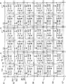
Fig. 2 is the structural drawing exemplified with the basic structure of the pixel electrode in display panel 40.The examples of combinations of pixel electrode in the situation that carrying out typical case's driving described later (the first drive pattern) that Fig. 2 has gone back schematic illustration.On the pixel electrode substrate of display panel 40, provide: a plurality of gate lines G 1, G2, the G3... for the scanning that extend in the horizontal direction, a plurality of source electrode line S1, S2, S3... to its input in response to the driving signal of received image signal, and a plurality of pixel electrode.A plurality of source electrode line S 1, S2, S3... extend in vertical direction, intersect with a plurality of gate lines G 1, G2, G3....Sub-pixel arrangements electrode one by one on the position of the intersection point corresponding to a plurality of gate lines G 1, G2, G3... and a plurality of source electrode line S 1, S2, S3....In the configuration example of Fig. 2, the pixel electrode that is connected to the first source electrode line S1 and the second source electrode line S2 is for red pixel electrode, and the pixel electrode that is connected to the 3rd source electrode line S3 and the 4th source electrode line S4 is for green pixel electrode.The pixel electrode that is connected to the 5th source electrode line S5 and the 6th source electrode line S6 is for blue pixel electrode.In addition,, in the description of this embodiment, statement " pixel " refers to the unit picture element of each color.
The switching device T of thin film transistor (TFT) is connected respectively to a plurality of pixel electrodes, and a plurality of pixel electrode can be distinguished independent control and driving.A plurality of pixel electrodes consist of two class pixel electrodes, and they are the first pixel electrode A and the second pixel electrode B with the area that is different from the first pixel electrode A.Alternately arrange two class pixel electrodes in the horizontal direction with in vertical direction.The second pixel electrode B has the larger area than the first pixel electrode A.When typical case drives (the first drive pattern), the first pixel electrode A adjacent one another are and the combination of the second pixel electrode B is in the horizontal direction taken as single pixel, and Execution driven.
Here, by utilizing the first pixel electrode 1A and the second pixel electrode 1B to be disposed in the example that the upper left side of Fig. 2 and another first pixel electrode 2A and another second pixel electrode 2B are disposed in the downside of the first pixel electrode 1A and the second pixel electrode 1B, specifically describe dot structure.In Fig. 2, for example, corresponding to being disposed in the part of upper left the first pixel electrode 1A, form pixel capacitance CL-RA1 and auxiliary capacitor CS-RA1.Pixel capacitance CL-RA1 is the electric capacity forming between the public electrode in the first pixel electrode 1A and unshowned opposite substrate side.Auxiliary capacitor CS-RA1 is the electric capacity forming between the first pixel electrode 1A and auxiliary capacitance bus.
The first pixel electrode 1A and the second pixel electrode 1B are connected to first grid polar curve G1 jointly by switching device TA1 and TB1.Another first pixel electrode 2A and another second pixel electrode 2B are connected to second gate line G2 jointly by other switching device TA2 and TB2.
Fig. 4 A is the key drawing exemplified with the example of the electrode shape of the first pixel electrode 1A and the second pixel electrode 1B and another first pixel electrode 2A and another second pixel electrode 2B.Here, the combination of the first pixel electrode 1A and the second pixel electrode 1B is taken as the first pixel, and the combination of another first pixel electrode 2A and another second pixel electrode 2B is taken as the second pixel.Now, arrange in the following manner electrode: the gravity position when the approximate combination formation region of the first pixel electrode 1A and the formation region of another first pixel electrode 2A is corresponding to the center that forms the whole region of the first pixel and the second pixel.
(circuit structure of drive control part)
Referring back to Fig. 1, circuit structure will be described.Timing controller 10 comprises receiving unit 11, data processing circuit 12, first memory controller 13, color correction circuit 14, overdrive circuit 15, second memory controller 16 and timing generator circuit part 17.Timing generator circuit part 17 comprises control signal generating portion 18, data formatter 19 and translator unit 20.
Here, under the first drive pattern, by a line, sequentially select a plurality of gate lines G 1, G2, the G3... on display panel 40, to pass through a plurality of pixel electrodes of horizon scan line.Under the second drive pattern, by two lines a plurality of gate lines G 1, G2, G3... on select progressively display panel 40 side by side, to scan continuously a plurality of pixel electrodes by two horizontal lines.The first drive pattern is the scan pattern of typical actuating speed, and the second drive pattern is the scan pattern for the double actuating speed Execution driven of standard of the actuating speed with the first drive pattern.
The operation setting of external ROM 22 storage timing controller 10 inside.For example, in timing controller 10, the image information that the first frame buffer 21 and the interim storage of the second frame buffer 23 are processed for carrying out the signal of inter frame image.It is unit that gate drivers 42 be take a horizontal line, opens the switching device T of each pixel electrode that is connected to display panel 40.Source electrode driver 41 offers by the electromotive force corresponding to showing data the horizontal pixel that gate drivers 42 is selected.
Receiving unit 11 receives the received image signal transmitting from outside.As received image signal, for example, input comprises the viewdata signal of R (redness), G (green) and B (blueness) and the signal of display control signal (vertical synchronizing signal Vsync, horizontal-drive signal Hsync and write control signal Enable).As shown in Figure 5A, for example, viewdata signal is sequentially alternately to comprise for image L1, the L2... of left eye with for the 3-D view signal of image R1, the R2... (having parallax between them) of right eye.For example, in the frame frequency cycle of 60Hz (16.6ms), comprise a left anaglyph and a right anaglyph.In the case, with 120Hz (8.3ms), upgrade each anaglyph.In the situation that demonstration has the image of the frame structure shown in Fig. 5 A, timing controller 10 drives display panel 40 under the first drive pattern, thereby as shown in Figure 5 B, by a horizon scan line display panel 40.
The frame rate of data processing circuit 12 conversion received image signals.First memory controller 13 is controlled the write and read of image information between data processing circuit 12 and the first frame buffer 21.
For example, data processing circuit 12 is converted to the view data as shown in Fig. 6 A or Fig. 7 A by input picture as shown in Figure 5A.In Fig. 6 A, the input picture of Fig. 5 A is converted into wherein identical anaglyph and arranges continuously the image of twice with the frame frequency cycle (16.6ms) of 60Hz.In the case, with 240Hz (4.17ms), upgrade each anaglyph.In Fig. 7 A, the input picture of Fig. 5 A is converted into the image that wherein inserts gray level image Gr between horizontal parallax image.In the case, with 240Hz (4.17ms), upgrade each anaglyph and gray level image Gr.Show that therein in the situation of the image with the frame structure as shown in Fig. 6 A and Fig. 7 A, timing controller 10 drives display panel 40 under the second drive pattern.In other words, as shown in Fig. 6 B and Fig. 7 B, by two horizontal line continuous sweep display panels 40, carry out and show thus.
Timing generator circuit part 17 is converted to the picture signal from overdrive circuit 15 for driving the signal of display panel 40, and this signal is offered to source electrode driver 41 and gate drivers 42.Data formatter 19 is according to the transfer system conversion image data array of source electrode driver 41.Translator unit 20 transmits according to the transfer system executive signal of source electrode driver 41.Control signal generating portion 18 offers source electrode driver 41 and gate drivers 42 by control signal.To gate drivers 42, control signal generating portion 18 is provided for scanning the horizontal gate drivers control signal on display panel 40.As driving signal, by translator unit 20, the signal in response to rgb image data is input to source electrode driver 41, and source electrode driver control signal is input to source electrode driver 41 from control signal generating portion 18.Source electrode driver control signal is to control each pixel being used for to display panel 40 to carry out the polarity of electromotive force and the signal of level conversion of writing.
(operation under the first drive pattern)
In this image display device, under the first drive pattern, the combination of the pixel electrode as shown in Fig. 2 and Fig. 4 A is used for carrying out and shows.In other words, gray-scale value based on differing from one another, drives the first pixel electrode (for example 1A) and the second pixel electrode (for example 1B) for example, along same gate line (G1), arranging adjacent to each other and for example, above arrange at two different source electrode lines (S1 and S2) in the horizontal direction.The combination of the first pixel electrode 1A and the second pixel electrode 1B is taken as single pixel, and carries out display driver.
The waveform of various driving signals in the situation that the part A of Fig. 8 arriving part K exemplified with execution demonstration under the first drive pattern.At the part A of Fig. 8 in part K, exemplified with show the situation of image with uniform luminance.The part A of Fig. 8 is exemplified with the example of the waveform of the initial timing signal GSTR of horizontal scanning.The part B of Fig. 8 is exemplified with the example of the waveform of the reference clock signal GCLK of horizontal scanning.The part C of Fig. 8 to part I exemplified with the example of waveform that is applied to the sweep signal of first grid polar curve G1 to the seven gate lines G 7.The part J of Fig. 8 is exemplified with the example of waveform that is applied to the picture signal of the first source electrode line S1.The part K of Fig. 8 is exemplified with the example of waveform that is applied to the picture signal of the second source electrode line S2.
Under the first drive pattern, if the part C of Fig. 8 is to as shown in part I, by each gate line of line sweep.When scanning first grid polar curve G1, as shown in the part J of Fig. 8, electromotive force V1+ (its absolute value to common potential VC is the electromotive force in the positive side of V1) is applied to the first source electrode line S1.Meanwhile, as shown in the part K of Fig. 8, electromotive force V3-(electromotive force on the minus side that its absolute value to common potential VC is V3) is applied to the second source electrode line S2.Absolute value V3 is set to less than the value of absolute value V1.In the case, for example, electromotive force V1+ is applied to the first pixel electrode 1A in Fig. 2, and electromotive force V3-is applied to the second pixel electrode 1B.Thereby, carry out shadow tone and drive, wherein the gray-scale value based on differing from one another drives the first pixel electrode 1A and the second pixel electrode 1B that forms as a whole a pixel, and has obtained the effect of the viewing angle characteristic that improves gray level.
(operation under the second drive pattern)
In this image display device, under the second drive pattern, the combination of the pixel electrode as shown in Fig. 3 and Fig. 4 B is used for carrying out and shows.Under the second drive pattern, by two lines, sequentially select a plurality of gate lines G 1, G2, G3..., to pass through two a plurality of pixel electrodes of horizon scan line simultaneously.In addition, the first pixel electrode and the second pixel electrode in the vertical direction on same source electrode line, arranging adjacent to each other and be disposed on two different gate lines are taken as single pixel, and carry out display driver.For example, as shown in Figure 3, the first pixel electrode 1A and another the second pixel electrode 2B that are connected to the first source electrode line S1 are taken as single pixel, and carry out display driver.In addition, for example, as shown in Figure 3, the second pixel electrode 1B and another the first pixel electrode 2A that are connected to the second source electrode line S2 are taken as single pixel, and carry out display driver.
Here, under the first drive pattern, be taken as in the combination of pixel electrode of single pixel, the combination of the first pixel electrode 1A and the second pixel electrode 1B is taken as the first pixel, and the combination of another first pixel electrode 2A and another second pixel electrode 2B is taken as the second pixel.Meanwhile, under the second drive pattern, when selecting first grid polar curve G1 and second gate line G2, consideration is disposed in each pixel electrode at the intersection point place of first grid polar curve G1 and second gate line G2 and the first source electrode line S1 and the second source electrode line S2 simultaneously.Under the second drive pattern, the second pixel electrode 1B on first grid polar curve G1 and another the first pixel electrode 2A on second gate line G2 are corresponding to the first pixel under the first drive pattern.In addition, the first pixel electrode 1A on first grid polar curve G1 and another the second pixel electrode 2B on second gate line G2 are corresponding to the second pixel under the first drive pattern.
The waveform of various driving signals in the situation that the part A of Fig. 9 arriving part K exemplified with execution demonstration under the second drive pattern.The part A of Fig. 9 is exemplified with the example of the waveform of the initial timing signal GSTR of horizontal scanning.The part B of Fig. 9 is exemplified with the example of the waveform of the reference clock signal GCLK of horizontal scanning.The part C of Fig. 9 to part I exemplified with the example of waveform that is applied to the sweep signal of first grid polar curve G1 to the seven gate lines G 7.The part J of Fig. 9 is exemplified with the example of waveform that is applied to the picture signal of the first source electrode line S1.The part K of Fig. 9 is exemplified with the example of waveform that is applied to the picture signal of the second source electrode line S2.
Under the second drive pattern, if the part C of Fig. 9 is to as shown in part I, by two each gate lines of line sweep.As shown in the part J of Fig. 9, electromotive force V15+ (its absolute value to common potential VC is the electromotive force in the positive side of V15) is applied to the first source electrode line S1.Meanwhile, as shown in the part K of Fig. 9, electromotive force V35-(electromotive force on the minus side that its absolute value to common potential VC is V35) is applied to the second source electrode line S2.Absolute value V35 is set to less than the value of absolute value V15.Thereby, corresponding to the pixel data of a pixel, be written on two pixel electrodes in vertical direction.
As mentioned above, according to the present embodiment, under the second drive pattern, because sequentially select a plurality of gate lines to pass through two a plurality of pixel electrodes of horizon scan line by two lines simultaneously, so likely obtain the actuating speed of the actuating speed twice that is the first drive pattern.Thereby for example, in the situation that display panel 40 has the driveability of 120Hz frame frequency, the standard that can carry out 240Hz frame frequency drives.
In this embodiment, particularly, under the second drive pattern, in the vertical direction on same source electrode line, be arranged to two pixel electrodes adjacent one another are and be taken as single pixel, and carry out display driver.Thereby, although can not carry out as the shadow tone driving under the first drive pattern, also likely obtain the actuating speed of the actuating speed twice that is the first drive pattern, and do not reduce display resolution.
2. the second embodiment
Then, will describe according to the image display device of second embodiment of the invention.In addition, by use identical Reference numeral represent with according to the practically identical assembly of the image display device of the first embodiment, thereby suitably omit and describe.
According in the image display device of this embodiment, the operation under the second drive pattern is different from the first embodiment.The base pixel structure (Fig. 2) of display panel 40 is identical with the first embodiment with the operation (Fig. 8) under the first drive pattern.
In this image display device, under the second drive pattern, the combination of pixel electrode is as shown in figure 10 used for carrying out and shows.Under the second drive pattern, by two lines, sequentially select a plurality of gate lines G 1, G2, G3..., to pass through two a plurality of pixel electrodes of horizon scan line simultaneously.In addition, under the second drive pattern, the combination that is disposed in four pixel electrodes in the intersection point of two source electrode lines adjacent one another are and two gate lines adjacent one another are is taken as single pixel, and carries out display driver.For example, two the pixel electrode 1B and the 2A that in two pixel electrode 1A that arrange continuously in vertical direction on the first source electrode line S1 and 2B and the vertical direction on the second source electrode line S2 adjacent to the first source electrode line S1, arrange are continuously combined and are used as single pixel, and carry out display driver.
In this embodiment, the waveform of various driving signals in the situation that the part A of Figure 11 arriving part K exemplified with execution demonstration under the second drive pattern.The part A of Figure 11 is exemplified with the example of the waveform of the initial timing signal GSTR of horizontal scanning.The part B of Figure 11 is exemplified with the example of the waveform of the reference clock signal GCLK of horizontal scanning.The part C of Figure 11 to part I exemplified with the example of waveform that is applied to the sweep signal of first grid polar curve G1 to the seven gate lines G 7.The part J of Figure 11 is exemplified with the example of waveform that is applied to the picture signal of the first source electrode line S1.The part K of Figure 11 is exemplified with the example of waveform that is applied to the picture signal of the second source electrode line S2.
Under the second drive pattern, if the part C of Figure 11 is to as shown in part I, by two each gate lines of line sweep.As shown in the part J of Figure 11, electromotive force V2+ (its absolute value to common potential VC is the electromotive force in the positive side of V2) is applied to the first source electrode line S1.Meanwhile, as shown in the part K of Figure 11, electromotive force V2-(electromotive force on the minus side that its absolute value to common potential VC is V2) is applied to the second source electrode line S2.In other words, absolute value is V2 and is applied to the first source electrode line S1 and the second source electrode line S2 with the in fact mutually the same electromotive force of pixel data.Thereby, corresponding to the pixel data of a pixel, be written into four pixel electrodes adjacent one another are in vertical direction and horizontal direction generally.
In this embodiment, because utilize identical image information to drive the first source electrode line S1 and the second source electrode line S2, so in the circuit of Fig. 1, the first frame buffer 21 can only be stored about will be for the information of the line side that drives.In other words, under the second drive pattern, by the horizontal Sparse (data-thinning) in every two horizontal lines from received image signal, generate picture signal, and the picture signal based on after Sparse drives display panel.Thereby, in signal bandwidth, allow some leeway, and likely improve for example performance of overdrive circuit 15.Likely by low speed between circuit, transmit data and reduce driving load.In addition, although reduced display resolution, likely obtain the actuating speed of the actuating speed twice that is the first drive pattern.
3. the 3rd embodiment
Then, will describe according to the image display device of third embodiment of the invention.In addition, by use identical Reference numeral indication with according to the practically identical assembly of the image display device of the first embodiment and the second embodiment, thereby suitably omit and describe.
Figure 12 is exemplified with according to the integrally-built block diagram of the image display device of this embodiment.Between the receiving unit 11 at timing controller 10A and data processing circuit 12, provide 3D gamma change-over circuit 24, the circuit structure of this image display device is identical with the circuit structure of Fig. 1.In this embodiment, Execution driven makes to be taken as the gray-scale value in the sub-pixel circuits of single pixel under the first drive pattern and the gray-scale value that is taken as under the second drive pattern in the sub-pixel circuits of single pixel differs from one another.Gamma characteristic under 3D gamma change-over circuit 24 conversion the second drive patterns.
Figure 13 is the block diagram exemplified with the first configuration example of 3D gamma change-over circuit 24.According to the 3D gamma change-over circuit 24 of this first configuration example, by LUT (ODD) 31, LUT (EVN) 32, first selector 33 and second selector 34, formed.LUT (ODD) the 31st, the LUT (look-up table) of the gamma table data of the pixel of the odd lines (source electrode line S1, S3, S5...) in storage vertical direction.LUT (EVN) the 32nd, the LUT (look-up table) of the gamma table data of the pixel of the even lines (source electrode line S2, S4, S6...) in storage vertical direction.First selector 33 is selected according to the parity of line and the output data of level conversion are carried out in output by LUT (ODD) 31 and LUT (EVN) 32.Second selector 34 is former state input-output data under the first drive pattern, and optionally exports the translation data of inputting by first selector 33 under the second drive pattern.
Figure 14 is the block diagram exemplified with the second configuration example of 3D gamma change-over circuit 24.Assembly in the first configuration example of Figure 13, the second configuration example also comprises First Line impact damper 35 and the second line buffer 36.In this second configuration example, by First Line impact damper 35 is provided, generate wire delay, and respectively to the view data of LUT (ODD) 31 and two lines of LUT (EVN) 32 inputs.In the second configuration example, each in LUT (ODD) 31 and LUT (EVN) 32 comprises the look-up table of two-dimensional arrangement, for according to correlativity (correlation) calculated correction value between two pixels.In the second configuration example, because generate the corrected value for the pixel of two lines simultaneously, so by the data of rear line data being carried out to wire delay and exporting data and converting video signal by the second line buffer 36 to the signal processing block of following stages.
By using the 3D gamma change-over circuit 24 in this second configuration example, in the second drive pattern, the pixel data of two pixels of arranging adjacent to each other in the first horizontal pixel line based on adjacent one another are in received image signal and the vertical direction on the second horizontal pixel line, determines and is applied to the signal level that is taken as the first pixel electrode of single pixel and the driving signal of the second pixel electrode.Driving circuit by following stages is input to the first pixel electrode and the second pixel electrode by a source electrode line by this driving signal.
Figure 15 is the block diagram exemplified with the 3rd configuration example of 3D gamma change-over circuit 24.In the 3rd configuration example, the function of the second configuration example of Figure 14 is further extended.Except the assembly of the first configuration example of Figure 13, the 3rd configuration example also comprises First Line impact damper 51, the second line buffer 52, the 3rd line buffer 53,3 * 3 wave filter (EVN) 54,3 * 3 wave filters (ODD) 55, coefficient correction circuit 56, the first addition/subtraction circuit 57, the second addition/subtraction circuit 58 and the 4th line buffer 59.First Line impact damper 51, the second line buffer 52 and the 3rd line buffer 53 are intended to generate three of received image signal horizontal delays.Thereby, can generate the odd lines and the upper lines of each pending pixel in even lines and the data of lower line that are arranged in vertical direction, and likely obtain the pixel data string of three lines that comprise pending pixel.The pixel data of these three lines is imported into 3 * 3 wave filters (EVN) 54 and 3 * 3 wave filters (ODD) 55.Each inside of 3 * 3 wave filters (EVN) 54 and 3 * 3 wave filters (ODD) 55 comprises a delay element, generate three horizontal delays, form 3 * 3 pixel datas, and generate filter coefficient by the operational symbol corresponding to 3 * 3 pixel datas is multiplied by 3 * 3 pixel datas.Coefficient correction circuit 56 is adjusted the filter coefficient generating.The first addition/subtraction circuit 57 adds/deducts filter coefficient to/from corrected value, and this corrected value obtains according to the correlativity between two pixels and exports from LUT (ODD) 31.The second addition/subtraction circuit 58 adds/deducts filter coefficient to/from corrected value, and this corrected value obtains according to the correlativity between two pixels and exports from LUT (EVN) 32.The 4th line buffer 59 has the function identical with the second line buffer 36 in the second configuration example, and the line data of dual numbers line are carried out wire delay.
By using the 3D gamma change-over circuit 24 of the 3rd configuration example, under the second drive pattern, the pixel data of two pixels of arranging adjacent to each other in the first horizontal pixel line based on adjacent one another are in received image signal and the vertical direction on the second horizontal pixel line, with the correlativity between near the pixel data of a plurality of other pixels two pixels, definite signal level that is taken as the first pixel electrode of single pixel and the driving signal of the second pixel electrode that is applied to.Driving circuit by following stages is input to the first pixel electrode and the second pixel electrode by a source electrode line by this driving signal.
Figure 16 is the performance plot exemplified with the gray level transmissison characteristic in each pixel electrode in the dot structure shown in Fig. 2 (the first drive pattern).Figure 17 is the performance plot exemplified with the gray level transmissison characteristic in each pixel electrode in the dot structure shown in Figure 10 (the second drive pattern).Display panel 40 has the gray level transmissison characteristic (gamma characteristic) for each pixel electrode, and the characteristic (Sub B) of the characteristic of the first pixel electrode A (Sub A) and the second pixel electrode B is added to obtain the gamma characteristic (Sub A+Sub B) of a pixel.
Under the first drive pattern, as shown in figure 16, utilize the gamma characteristic of the first pixel electrode A and the gamma characteristic of the second pixel electrode B that differ from one another, carry out Execution driven.Preferably, for fear of viewing angle characteristic poor transmissive state under low gray level, gamma characteristic as shown in figure 16.Under the second drive pattern, as shown in figure 17, by the Area Ratio of each pixel electrode being multiplied by predetermined synthetic gamma characteristic (Sub A+Sub B), obtain the gamma characteristic of the first pixel electrode A and the second pixel electrode B.
4. the 4th embodiment
Then, will describe according to the image display device of fourth embodiment of the invention.In addition, by use identical Reference numeral represent with according to the practically identical assembly of the assembly of the image display device of the first embodiment to the three embodiment, thereby suitably omit and describe.
According in the image display device of this embodiment, the operation under the second drive pattern is different from the first embodiment.In addition, base pixel structure (Fig. 2) difference of display panel 40.
In this image display device, under the second drive pattern, by using the combination of pixel electrode as shown in figure 18 to carry out, show.In this embodiment, in display panel 40, alternately arrange in the horizontal direction two class pixel electrodes, and the pixel electrode of same type periodically occurs according to two lines in vertical direction.For example, be arranged in the upper left pixel of Figure 18, two pixel electrode 1A and 2A in vertical direction are the first pixel electrodes.In addition, two other pixel electrode 1B and the 2B adjacent with 2A with two pixel electrode 1A is the second pixel electrode in vertical direction.
In this embodiment, although the cycle that pixel electrode occurs be in vertical direction different from the situation of Fig. 2, under the first drive pattern, because carry out scanning by horizontal line, so those of basic operation and the first embodiment are identical.And, in this embodiment, under the first drive pattern, two pixel electrodes according to the gray-scale value driving based on differing from one another in the horizontal direction that forms as a whole a pixel (for example, pixel electrode 1A and 1B) mode, execution shadow tone drives, and the effect of the viewing angle characteristic of the gray level that is likely improved.
Under the second drive pattern, by two lines, sequentially select a plurality of gate lines G 1, G2, G3..., to pass through two a plurality of pixel electrodes of horizon scan line simultaneously.In addition, in the vertical direction on same source electrode line, the first pixel electrode and the second pixel electrode adjacent one another are and that be disposed on different gate lines are taken as the unit picture element that will drive, and carry out display driver.For example, as shown in figure 18, the first pixel electrode 1A and another the first pixel electrode 2A that are connected to the first source electrode line S1 are taken as first unit picture element that will drive, and carry out display driver.In addition, for example, the second pixel electrode 1B and another the second pixel electrode 2B that are connected to the second source electrode line S2 are taken as second unit picture element that will drive, and carry out display driver.The pixel electrode of the pixel electrode of the first unit picture element in the case, to be driven and the second unit picture element to be driven is driven to has the gray-scale value differing from one another in horizontal direction.Combine in the horizontal direction the pixel electrode of the first unit picture element to be driven and the pixel electrode of the second unit picture element to be driven, and be used as single pixel to carry out display driver.
The waveform of various driving signals in the situation that the part A of Figure 19 arriving part K exemplified with execution demonstration under the second drive pattern.The part A of Figure 19 is exemplified with the example of the waveform of the initial timing signal GSTR of horizontal scanning.The part B of Figure 19 is exemplified with the example of the waveform of the reference clock signal GCLK of horizontal scanning.The part C of Figure 19 to part I exemplified with the example of waveform that is applied to the sweep signal of first grid polar curve G1 to the seven gate lines G 7.The part J of Figure 19 is exemplified with the example of waveform that is applied to the picture signal of the first source electrode line S1.The part K of Figure 19 is exemplified with the example of waveform that is applied to the picture signal of the second source electrode line S2.
Under the second drive pattern, if the part C of Figure 19 is to as shown in part I, by two each gate lines of line sweep.When scanning first grid polar curve G1 and second gate line G2, as shown in the part J of Figure 19, electromotive force V1+ (its absolute value to common potential VC is the electromotive force in the positive side of V1) is applied to the first source electrode line S1.Meanwhile, as shown in the part K of Figure 19, electromotive force V3-(electromotive force on the minus side that its absolute value to common potential VC is V3) is applied to the second source electrode line S2.Absolute value V3 is set to less than the value of absolute value V1.In the case, for example, electromotive force V1+ is applied to the first pixel electrode 1A and the 2A of two in vertical direction in Figure 18.Electromotive force V3-is applied to the second pixel electrode 1B and 2B in vertical direction.
In this embodiment, under the second drive pattern, because sequentially select a plurality of gate lines to pass through two a plurality of pixel electrodes of horizon scan line by two lines simultaneously, so likely obtain the actuating speed of the actuating speed twice that is the first drive pattern.Now, because two the second pixel electrode 1B that arrange continuously in two the first pixel electrode 1A that arrange continuously in the vertical direction on the first source electrode line S1 and 2A and the vertical direction on the second source electrode line S2 and 2B are driven to, there is the gray-scale value differing from one another, so likely carry out shadow tone, drive that actuating speed is double simultaneously.Thereby, although reduced display resolution, likely obtain the actuating speed of the actuating speed twice of the first drive pattern, the effect of the viewing angle characteristic of the gray level that is simultaneously improved.
5. other embodiment
In the present invention, can carry out various modifications and be not limited to previous embodiment.For example, in the aforementioned embodiment, under the second drive pattern, although described simultaneously, by two (N=2) lines, sequentially select many gate lines with by the situation of two a plurality of pixel electrodes of horizon scan line, can by N=3 bar line or more lines, sequentially carry out scanning simultaneously.For example, in the 4th embodiment (Figure 18 and Figure 19), in the pixel layout periodically occurring by three or more lines in vertical direction at the pixel electrode of same type, can sequentially scan three or more lines simultaneously.
In the case, under the second drive pattern, by every N bar horizontal (N-1) bar horizontal line to from received image signal, carry out Sparse and synthetic image signal, and the picture signal based on after Sparse drives display panel.Under the second drive pattern, can in sweep time, carry out at the 1/N of the first drive pattern the scanning of a screen.For example, can in following situation, use the second drive pattern: in a frame period, carry out and control, make to be shown N time continuously for the identical image of left eye, and showing for showing N time continuously before or after the image of left eye for the identical image of right eye.
In addition, in the aforementioned embodiment, although described as received image signal input and comprised that in chronological order driving method of the present invention also can be applicable to the signal except this 3-D view signal for the image of left eye with for the example of the 3-D view of the image (having parallax between them) of right eye.
The present invention comprises the relevant theme of Japanese priority patent application JP2009-230318 that Japan Office submitted to October 2 in 2009, and its full content is incorporated herein by reference.
It will be understood by those skilled in the art that and can carry out various modifications, combination, sub-portfolio and replacement according to design requirement and other factors, as long as they are in the scope of claims or its equivalent.
Claims (14)
1. an image display device, comprising:
Display panel, comprise in the horizontal direction extend for many gate lines, many source electrode lines that intersect with described many gate lines that extend in vertical direction that scan and be arranged in one by one the locational a plurality of pixel electrodes corresponding with the intersection point of described many gate lines and many source electrode lines, described source electrode line is supplied with the driving signal based on received image signal, and each pixel electrode is controlled to drive by independent; And
Drive control part, by optionally controlling with the driving that the first drive pattern and these two drive patterns of the second drive pattern are carried out display panel, on described display panel, show thus the image based on described received image signal, described the first drive pattern allows described a plurality of pixel electrodes horizontal line by many gate lines described in select progressively seriatim by a line scan, and described the second drive pattern horizontal line of allowing described a plurality of pixel electrodes by many gate lines described in the ground select progressively of N bar line by a N bar line scan, wherein N is 2 or larger integer, wherein
Under described the first drive pattern, described drive control part is carried out display driver in the following manner, i.e. two corresponding gray-scale values based on differing from one another and drive a pair of pixel electrode and this combination to pixel electrode to be taken as the mode of single pixel, this is arranged to along gate line adjacent one another are and be disposed on two respective sources polar curves in the horizontal direction to pixel electrode, and
Under described the second drive pattern, described drive control part is carried out display driver in the following manner, and N the pixel electrode of arranging continuously in vertical direction along source electrode line is taken as the mode of unit picture element to be driven,
The combination wherein with two pixel electrodes of the area differing from one another is taken as single pixel.
2. image display device according to claim 1, wherein
Described display panel configures in the following manner, wherein alternately arranges in the horizontal direction and in vertical direction the first pixel electrode and second pixel electrode with the area that is different from the first pixel electrode,
Under described the first drive pattern, described drive control part is carried out display driver in the following manner, wherein two corresponding gray-scale values based on differing from one another drive along gate line and arrange and be disposed in adjacent to each other in the horizontal direction the first and second pixel electrodes on two respective sources polar curves, and the combination of described the first and second pixel electrodes is taken as single pixel, and
Under described the second drive pattern, described drive control part is carried out display driver in the following manner, wherein by many gate lines described in two lines ground select progressivelys once, carry out once to scan the horizontal line of described a plurality of pixel electrodes, and the first and second pixel electrodes of all arranging adjacent to each other in vertical direction and arrange along two respective gates lines along source electrode line are taken as single pixel two lines.
3. image display device as claimed in claim 2, wherein
The area of described the second pixel electrode is set to larger than the area of described the first pixel electrode, and
Under described the first drive pattern, described drive control part is carried out display driver in the following manner, the combination of the first and second pixel electrodes of wherein arranging at the intersection point place of first grid polar curve and the first and second source electrode lines disposed adjacent one another is taken as the first pixel, and be taken as the second pixel at another first pixel electrode of the intersection point place of the second gate line of arranging adjacent to described first grid polar curve and described the first and second source electrode lines layout and the combination of another the second pixel electrode, and
Under described the second drive pattern, described drive control part is selected described the first and second gate lines simultaneously, to carry out in the following manner display driver, wherein along the second pixel electrode of first grid polar curve with along the combination of described another first pixel electrode of second gate line, be taken as the first pixel, and be taken as the second pixel along the first pixel electrode of first grid polar curve with along the combination of described another second pixel electrode of second gate line.
4. image display device as claimed in claim 2, wherein
Described drive control part is carried out display driver in the following manner, and the gray-scale data wherein applying to the pixel electrode that is taken as single pixel under the first drive pattern is different from the gray-scale data applying to the pixel electrode that is taken as single pixel under the second drive pattern.
5. image display device as claimed in claim 2, wherein
Under described the second drive pattern, described drive control part is based on disposed adjacent one another and belong to the pixel data in the received image signal of corresponding first and second horizontal two pixels disposed adjacent one another in vertical direction, determine the signal level of the driving signal that will apply to corresponding the first and second pixel electrodes that are taken as single pixel, and
Described drive control part offers respectively the first and second pixel electrodes by a source electrode line by described driving signal.
6. image display device as claimed in claim 2, wherein
Under described the second drive pattern, the correlativity of described drive control part based between the pixel data of two pixels in received image signal and the pixel data of a plurality of other pixels, determine the signal level of the driving signal that will apply to corresponding the first and second pixel electrodes that are taken as single pixel, described two pixels are arranged adjacent to each other in vertical direction and are belonged to corresponding the first and second horizontal lines disposed adjacent one another, described a plurality of other pixel is positioned near described two pixels, and
Described drive control part offers corresponding the first and second pixel electrodes by a source electrode line by described driving signal.
7. image display device as claimed in claim 2, wherein
The area of described the second pixel electrode is set to larger than the area of described the first pixel electrode, and
Under described the first drive pattern, described drive control part is carried out display driver in the following manner, the combination of the first and second pixel electrodes of wherein arranging at the intersection point place of first grid polar curve and the first and second source electrode lines disposed adjacent one another is taken as the first pixel, and be taken as the second pixel at another first pixel electrode of the intersection point place of the second gate line of arranging adjacent to described first grid polar curve and described the first and second source electrode lines layout and the combination of another the second pixel electrode, and
As the gravity position of combination zone of combination in region that forms the region of the first pixel electrode on described first grid polar curve and form another the first pixel electrode on described second gate line corresponding to the center that forms the overall region of described the first and second pixels.
8. image display device as claimed in claim 1, wherein
Described display panel configures in the following manner, and wherein the first pixel electrode is alternately arranged in the horizontal direction with second pixel electrode with the area that is different from the first pixel electrode, and according to the cycle of N bar line, alternately arranges in vertical direction,
Under described the first drive pattern, described drive control part is carried out display driver in the following manner, wherein two corresponding gray-scale values based on differing from one another drive along gate line and arrange adjacent to each other in the horizontal direction and be disposed in the first and second pixel electrodes on two respective sources polar curves, and the combination of described the first and second pixel electrodes is taken as single pixel, and
Under described the second drive pattern, described drive control part is carried out display driver in the following manner, wherein the combination of N the first pixel electrode and N the second pixel electrode is taken as single pixel, described N the first pixel electrode arranged in vertical direction continuously along the first source electrode line, and described N the second pixel electrode arranged in vertical direction continuously along the second source electrode line adjacent to described the first source electrode line, and based on two that differ from one another corresponding gray-scale value driving N the first pixel electrode and N the second pixel electrode.
9. image display device as claimed in claim 8, wherein
Under described the second drive pattern, described drive control part for every N bar horizontal line, by rarefaction (N-1) bar horizontal line, received image signal is applied to Sparse and processes, and the picture signal based on gained drives described display panel.
10. image display device as claimed in claim 1, wherein
Under described the second drive pattern, described control drive part scans a screen in the sweep time of the 1/N of the sweep time under described the first drive pattern.
11. image display devices as claimed in claim 1, wherein
The 3-D view signal that comprises in chronological order left-eye image and the eye image with parallax to described drive control part input therebetween, as described received image signal, and
Under described the second drive pattern, in a frame period, described control drive part repeats to show left-eye image N time continuously, and repeats continuously to show eye image N time before or after showing described left-eye image.
12. 1 kinds of image display devices, comprising:
Display panel, comprise in the horizontal direction extend for many gate lines, many source electrode lines that intersect with described many gate lines that extend in vertical direction that scan and be arranged in one by one the locational a plurality of pixel electrodes corresponding with the intersection point of described many gate lines and many source electrode lines, described source electrode line is supplied with the driving signal based on received image signal, and each pixel electrode is controlled to drive by independent; And
Drive control part, by the driving of optionally using these two drive patterns of the first drive pattern and the second drive pattern to carry out display panel, control, on described display panel, show thus the image based on described received image signal, described the first drive pattern allows described a plurality of pixel electrodes horizontal line by many gate lines described in select progressively one by one by a line scan, and described the second drive pattern horizontal line of allowing described a plurality of pixel electrodes by many gate lines described in the ground select progressively of N bar line by a N bar line scan, wherein N is 2 or larger integer, wherein
Under described the first drive pattern, described drive control part is carried out display driver in the following manner, two corresponding gray-scale values based on differing from one another and drive a pair of pixel electrode wherein, and this combination to pixel electrode is taken as single pixel, this is arranged to along gate line adjacent one another are and be disposed on two respective sources polar curves in the horizontal direction to pixel electrode, and
Under described the second drive pattern, described drive control part is carried out display driver in the following manner, wherein the combination of N the first pixel electrode and N the second pixel electrode is taken as single pixel, described N the first pixel electrode arranged in vertical direction continuously along the first source electrode line, and described N the second pixel electrode arranged in vertical direction continuously along the second source electrode line adjacent to described the first source electrode line
The combination wherein with two pixel electrodes of the area differing from one another is taken as single pixel.
13. 1 kinds of methods that drive image display device by drive control part, described image display device is controlled display panel, described display panel comprise in the horizontal direction extend for many gate lines, many source electrode lines that intersect with described many gate lines that extend in vertical direction that scan and be arranged in one by one the locational a plurality of pixel electrodes corresponding with the intersection point of described many gate lines and many source electrode lines, described source electrode line is supplied with the driving signal based on received image signal, each pixel electrode is controlled to drive by independent, wherein
Described drive control part is by optionally controlling with the driving that the first drive pattern and these two drive patterns of the second drive pattern are carried out display panel, on described display panel, show thus the image based on described received image signal, described the first drive pattern allows described a plurality of pixel electrodes horizontal line by many gate lines described in select progressively seriatim by a line scan, and described the second drive pattern horizontal line of allowing described a plurality of pixel electrodes by many gate lines described in the ground select progressively of N bar line by a N bar line scan, wherein N is 2 or larger integer,
Under described the first drive pattern, described drive control part is carried out display driver in the following manner, two corresponding gray-scale values based on differing from one another and drive a pair of pixel electrode wherein, and this combination to pixel electrode is taken as single pixel, this is arranged to along gate line adjacent one another are and be disposed on two respective sources polar curves in the horizontal direction to pixel electrode, and
Under described the second drive pattern, described drive control part is carried out display driver in the following manner, and N the pixel electrode of wherein arranging continuously in vertical direction along source electrode line is taken as unit picture element to be driven,
The combination wherein with two pixel electrodes of the area differing from one another is taken as single pixel.
14. 1 kinds of methods that drive image display device by drive control part, described image display device is controlled display panel, described display panel comprise in the horizontal direction extend for many gate lines, many source electrode lines that intersect with described many gate lines that extend in vertical direction that scan and be arranged in one by one the locational a plurality of pixel electrodes corresponding with the intersection point of described many gate lines and many source electrode lines, described source electrode line is supplied with the driving signal based on received image signal, each pixel electrode is controlled to drive by independent, wherein
Described drive control part is by optionally controlling with the driving that the first drive pattern and these two drive patterns of the second drive pattern are carried out display panel, on described display panel, show thus the image based on described received image signal, described the first drive pattern allows described a plurality of pixel electrodes horizontal line by many gate lines described in select progressively seriatim by a line scan, and described the second drive pattern horizontal line of allowing described a plurality of pixel electrodes by many gate lines described in the ground select progressively of N bar line by a N bar line scan, wherein N is 2 or larger integer,
Under described the first drive pattern, described drive control part is carried out display driver in the following manner, two corresponding gray-scale values based on differing from one another and drive a pair of pixel electrode wherein, and this combination to pixel electrode is taken as single pixel, this is arranged to along gate line adjacent one another are and be disposed on two respective sources polar curves in the horizontal direction to pixel electrode, and
Under described the second drive pattern, described drive control part is carried out display driver in the following manner, wherein the combination of N the first pixel electrode and N the second pixel electrode is taken as single pixel, described N the first pixel electrode arranged in vertical direction continuously along the first source electrode line, and described N the second pixel electrode arranged in vertical direction continuously by the second source electrode line along adjacent to described the first source electrode line
The combination wherein with two pixel electrodes of the area differing from one another is taken as single pixel.
Applications Claiming Priority (2)
| Application Number | Priority Date | Filing Date | Title |
|---|---|---|---|
| JP2009230318A JP2011076034A (en) | 2009-10-02 | 2009-10-02 | Image display device and method for driving the same |
| JP230318/09 | 2009-10-02 |
Publications (2)
| Publication Number | Publication Date |
|---|---|
| CN102034448A CN102034448A (en) | 2011-04-27 |
| CN102034448B true CN102034448B (en) | 2014-02-12 |
Family
ID=43887260
Family Applications (1)
| Application Number | Title | Priority Date | Filing Date |
|---|---|---|---|
| CN201010294273.3A Expired - Fee Related CN102034448B (en) | 2009-10-02 | 2010-09-25 | Image display device and method of driving image display device |
Country Status (5)
| Country | Link |
|---|---|
| US (1) | US8564627B2 (en) |
| JP (1) | JP2011076034A (en) |
| KR (1) | KR20110036670A (en) |
| CN (1) | CN102034448B (en) |
| TW (1) | TWI435297B (en) |
Families Citing this family (48)
| Publication number | Priority date | Publication date | Assignee | Title |
|---|---|---|---|---|
| CN105468895A (en) | 2006-05-02 | 2016-04-06 | 普罗透斯数字保健公司 | Patient customized therapeutic regimens |
| KR101611240B1 (en) | 2006-10-25 | 2016-04-11 | 프로테우스 디지털 헬스, 인코포레이티드 | Controlled activation ingestible identifier |
| CA2676407A1 (en) | 2007-02-01 | 2008-08-07 | Proteus Biomedical, Inc. | Ingestible event marker systems |
| CA2676280C (en) | 2007-02-14 | 2018-05-22 | Proteus Biomedical, Inc. | In-body power source having high surface area electrode |
| US8540632B2 (en) | 2007-05-24 | 2013-09-24 | Proteus Digital Health, Inc. | Low profile antenna for in body device |
| ES2696984T3 (en) | 2008-07-08 | 2019-01-21 | Proteus Digital Health Inc | Ingestion event marker data infrastructure |
| WO2010080843A2 (en) | 2009-01-06 | 2010-07-15 | Proteus Biomedical, Inc. | Ingestion-related biofeedback and personalized medical therapy method and system |
| TWI517050B (en) | 2009-11-04 | 2016-01-11 | 普羅托斯數位健康公司 | System for supply chain management |
| TWI557672B (en) | 2010-05-19 | 2016-11-11 | 波提亞斯數位康健公司 | Computer system and computer-implemented method to track medication from manufacturer to a patient, apparatus and method for confirming delivery of medication to a patient, patient interface device |
| US20130181968A1 (en) * | 2010-09-21 | 2013-07-18 | Sharp Kabushiki Kaisha | Drive circuit of display device, display device, and method of driving display device |
| KR101783259B1 (en) * | 2010-12-31 | 2017-10-10 | 삼성디스플레이 주식회사 | Method for compensating data, compensating apparatus for performing the method and display device having the compensating apparatus |
| KR20120114022A (en) * | 2011-04-06 | 2012-10-16 | 삼성디스플레이 주식회사 | Three dimensional image display device |
| KR101860083B1 (en) | 2011-06-29 | 2018-05-23 | 삼성디스플레이 주식회사 | 3 dimensional image display device and driving method thereof |
| WO2015112603A1 (en) | 2014-01-21 | 2015-07-30 | Proteus Digital Health, Inc. | Masticable ingestible product and communication system therefor |
| US9756874B2 (en) | 2011-07-11 | 2017-09-12 | Proteus Digital Health, Inc. | Masticable ingestible product and communication system therefor |
| KR101446381B1 (en) * | 2011-07-15 | 2014-10-02 | 엘지디스플레이 주식회사 | Image display device |
| CN103827914A (en) | 2011-07-21 | 2014-05-28 | 普罗秋斯数字健康公司 | Mobile communication device, system, and method |
| KR20130032161A (en) * | 2011-09-22 | 2013-04-01 | 삼성전자주식회사 | Method for driving display panel and display apparatus thereof |
| JP2013073036A (en) | 2011-09-28 | 2013-04-22 | Seiko Epson Corp | Electro-optical device and electronic apparatus |
| KR101950204B1 (en) * | 2011-09-30 | 2019-02-25 | 삼성디스플레이 주식회사 | Method of driving display panel and display apparatus for performing the same |
| WO2013051466A1 (en) * | 2011-10-03 | 2013-04-11 | シャープ株式会社 | Display device and method for driving same |
| US8665264B2 (en) | 2011-11-23 | 2014-03-04 | Shenzhen China Star Optoelectronics Technology Co., Ltd. | LCD panel and LCD device |
| CN102411241B (en) * | 2011-11-23 | 2014-06-18 | 深圳市华星光电技术有限公司 | Liquid crystal display panel and liquid crystal display device |
| US20130141472A1 (en) * | 2011-12-02 | 2013-06-06 | Xiao-Ping Tan | Liquid crystal stereoscopic display system and a method for driving the same |
| KR20130079044A (en) * | 2012-01-02 | 2013-07-10 | 삼성전자주식회사 | Display apparatus and control method thereof |
| CN102568424A (en) * | 2012-02-09 | 2012-07-11 | 华映视讯(吴江)有限公司 | Circuit and method for outputting over-driving voltages of liquid crystal panel |
| JP5893449B2 (en) * | 2012-03-09 | 2016-03-23 | 株式会社ジャパンディスプレイ | Display device and electronic device |
| KR101477967B1 (en) * | 2012-03-12 | 2014-12-31 | 삼성디스플레이 주식회사 | Method of driving display panel and display apparatus for performing the same |
| KR20130109816A (en) * | 2012-03-28 | 2013-10-08 | 삼성디스플레이 주식회사 | 3d image display device and driving method thereof |
| JP5943707B2 (en) * | 2012-05-25 | 2016-07-05 | 三菱電機株式会社 | Image display device |
| KR102020354B1 (en) * | 2013-03-12 | 2019-11-05 | 삼성디스플레이 주식회사 | Display apparatus |
| JP6511439B2 (en) | 2013-06-04 | 2019-05-15 | プロテウス デジタル ヘルス, インコーポレイテッド | Systems, devices, and methods for data collection and outcome assessment |
| US10084880B2 (en) | 2013-11-04 | 2018-09-25 | Proteus Digital Health, Inc. | Social media networking based on physiologic information |
| KR102284714B1 (en) * | 2014-12-30 | 2021-08-02 | 엘지디스플레이 주식회사 | Stereoscopic image display apparatus |
| CN104849929B (en) * | 2015-05-06 | 2018-09-04 | 深圳市华星光电技术有限公司 | Liquid crystal display panel and liquid crystal display device |
| CN104916250B (en) * | 2015-06-26 | 2018-03-06 | 合肥鑫晟光电科技有限公司 | A kind of data transmission method and device, display device |
| CN105161059B (en) * | 2015-06-30 | 2018-09-07 | 京东方科技集团股份有限公司 | Display drive method, display panel and preparation method thereof, display device |
| CN104978944A (en) * | 2015-08-06 | 2015-10-14 | 京东方科技集团股份有限公司 | Driving method for display panel, display panel and display device |
| CN104966506B (en) * | 2015-08-06 | 2017-06-06 | 京东方科技集团股份有限公司 | The driving method and relevant apparatus of a kind of shift register, display panel |
| CN105096865B (en) * | 2015-08-06 | 2018-09-07 | 京东方科技集团股份有限公司 | Output control unit, shift register and its driving method and gate drive apparatus of shift register |
| CN109843149B (en) | 2016-07-22 | 2020-07-07 | 普罗秋斯数字健康公司 | Electromagnetic sensing and detection of ingestible event markers |
| CN107230447A (en) * | 2017-08-04 | 2017-10-03 | 京东方科技集团股份有限公司 | A kind of driving method, drive circuit and display panel |
| CN107833550A (en) * | 2017-10-27 | 2018-03-23 | 友达光电(苏州)有限公司 | Display device and its clock pulse generator |
| CN108389557B (en) * | 2018-03-16 | 2020-01-21 | 京东方科技集团股份有限公司 | Display device and driving method thereof |
| KR102558106B1 (en) * | 2018-05-30 | 2023-07-21 | 엘지디스플레이 주식회사 | Display panel, display device and virtual reality/augmented reality device |
| KR20200040982A (en) * | 2018-10-10 | 2020-04-21 | 삼성디스플레이 주식회사 | Display apparatus and method of driving display panel using the same |
| CN111028799B (en) * | 2019-12-10 | 2021-09-03 | Tcl华星光电技术有限公司 | Driving circuit and driving method of display panel |
| KR20220049216A (en) * | 2020-10-14 | 2022-04-21 | 삼성전자주식회사 | Display apparatus and the control method thereof |
Citations (3)
| Publication number | Priority date | Publication date | Assignee | Title |
|---|---|---|---|---|
| CN1444196A (en) * | 2002-03-07 | 2003-09-24 | 株式会社日立制作所 | Display device and its driving method |
| CN1694152A (en) * | 2004-04-30 | 2005-11-09 | 富士通显示技术株式会社 | Liquid crystal display device with improved viewing angle characteristics |
| CN101546542A (en) * | 2008-03-24 | 2009-09-30 | 索尼株式会社 | Liquid crystal display device, liquid crystal display method, display control device, and display control method |
Family Cites Families (8)
| Publication number | Priority date | Publication date | Assignee | Title |
|---|---|---|---|---|
| KR0171938B1 (en) * | 1994-08-25 | 1999-03-20 | 사토 후미오 | Liquid crystal display device |
| US5808594A (en) * | 1994-09-26 | 1998-09-15 | Canon Kabushiki Kaisha | Driving method for display device and display apparatus |
| JPH1195722A (en) | 1997-09-17 | 1999-04-09 | Sanyo Electric Co Ltd | Stereoscopic video display method for time division glasses system using plasma display panel |
| JP3832439B2 (en) * | 2003-02-19 | 2006-10-11 | ソニー株式会社 | Display device and driving method thereof |
| JP2004258139A (en) * | 2003-02-24 | 2004-09-16 | Sharp Corp | Liquid crystal display device |
| TWI344560B (en) * | 2006-06-02 | 2011-07-01 | Au Optronics Corp | Array substrate and panel of liquid crystal display |
| JP5069946B2 (en) * | 2007-05-16 | 2012-11-07 | 株式会社ジャパンディスプレイイースト | Liquid crystal display |
| JP5309488B2 (en) * | 2007-07-18 | 2013-10-09 | セイコーエプソン株式会社 | Electro-optical device and electronic apparatus |
-
2009
- 2009-10-02 JP JP2009230318A patent/JP2011076034A/en active Pending
-
2010
- 2010-09-16 KR KR1020100090881A patent/KR20110036670A/en not_active Application Discontinuation
- 2010-09-23 US US12/924,216 patent/US8564627B2/en not_active Expired - Fee Related
- 2010-09-24 TW TW099132394A patent/TWI435297B/en not_active IP Right Cessation
- 2010-09-25 CN CN201010294273.3A patent/CN102034448B/en not_active Expired - Fee Related
Patent Citations (3)
| Publication number | Priority date | Publication date | Assignee | Title |
|---|---|---|---|---|
| CN1444196A (en) * | 2002-03-07 | 2003-09-24 | 株式会社日立制作所 | Display device and its driving method |
| CN1694152A (en) * | 2004-04-30 | 2005-11-09 | 富士通显示技术株式会社 | Liquid crystal display device with improved viewing angle characteristics |
| CN101546542A (en) * | 2008-03-24 | 2009-09-30 | 索尼株式会社 | Liquid crystal display device, liquid crystal display method, display control device, and display control method |
Non-Patent Citations (1)
| Title |
|---|
| JP特开平11-95722A 1999.04.09 |
Also Published As
| Publication number | Publication date |
|---|---|
| KR20110036670A (en) | 2011-04-08 |
| JP2011076034A (en) | 2011-04-14 |
| CN102034448A (en) | 2011-04-27 |
| US8564627B2 (en) | 2013-10-22 |
| US20110169871A1 (en) | 2011-07-14 |
| TW201128605A (en) | 2011-08-16 |
| TWI435297B (en) | 2014-04-21 |
Similar Documents
| Publication | Publication Date | Title |
|---|---|---|
| CN102034448B (en) | Image display device and method of driving image display device | |
| KR101477967B1 (en) | Method of driving display panel and display apparatus for performing the same | |
| CN101339315B (en) | Liquid crystal display apparatus | |
| CN101751889B (en) | Liquid crystal display | |
| US9618758B2 (en) | Stereoscopic image display and method of controlling backlight thereof | |
| CN102547335B (en) | Stereoscopic image display and driving method thereof | |
| US8803953B2 (en) | Stereoscopic image display device and driving method thereof | |
| CN101923221B (en) | Image display device and image display system using same | |
| CN102193239A (en) | Stereoscopic image display and driving method thereof | |
| CN101833906A (en) | Liquid crystal display and driving method thereof | |
| CN103728751B (en) | Switch the liquid crystal display of display two and three dimensions image | |
| CN103813157A (en) | Autostereoscopic image display and method for driving the same | |
| KR20110138677A (en) | Timing control unit and apparatus and method for displaying using thereof | |
| JP2013198166A (en) | Display apparatus | |
| CN104253987B (en) | Stereoscopic image display and driving method thereof | |
| CN103728752B (en) | Improve the liquid crystal display that flicker occurs display 3D image | |
| CN103108205B (en) | stereoscopic display system | |
| CN103617785B (en) | A kind of three-dimensional liquid crystal display device and display control method | |
| CN103037232B (en) | Stereoscopic image display | |
| CN100555033C (en) | Data converting and method thereof and have the liquid crystal display device of this device | |
| CN102385847B (en) | Liquid crystal display and driving method thereof | |
| KR101773609B1 (en) | Stereoscopic image display and driving method thereof | |
| KR101972489B1 (en) | Stereoscopic image display and gamma compensation method thereof | |
| KR101712207B1 (en) | Stereoscopic image display and over driving method | |
| WO2012073731A1 (en) | Liquid crystal display device, stereoscopic display system, control program, and recording medium |
Legal Events
| Date | Code | Title | Description |
|---|---|---|---|
| C06 | Publication | ||
| PB01 | Publication | ||
| C10 | Entry into substantive examination | ||
| SE01 | Entry into force of request for substantive examination | ||
| C14 | Grant of patent or utility model | ||
| GR01 | Patent grant | ||
| CF01 | Termination of patent right due to non-payment of annual fee |
Granted publication date: 20140212 Termination date: 20150925 |
|
| EXPY | Termination of patent right or utility model |