CN1020239C - Method of forming high temp. barriers in structural metals to make such metals creep resistant at high homologous temp. - Google Patents
Method of forming high temp. barriers in structural metals to make such metals creep resistant at high homologous temp. Download PDFInfo
- Publication number
- CN1020239C CN1020239C CN89107597A CN89107597A CN1020239C CN 1020239 C CN1020239 C CN 1020239C CN 89107597 A CN89107597 A CN 89107597A CN 89107597 A CN89107597 A CN 89107597A CN 1020239 C CN1020239 C CN 1020239C
- Authority
- CN
- China
- Prior art keywords
- layer
- metal
- structural metal
- ion
- creep
- Prior art date
- Legal status (The legal status is an assumption and is not a legal conclusion. Google has not performed a legal analysis and makes no representation as to the accuracy of the status listed.)
- Expired - Fee Related
Links
Images

Classifications
-
- B—PERFORMING OPERATIONS; TRANSPORTING
- B32—LAYERED PRODUCTS
- B32B—LAYERED PRODUCTS, i.e. PRODUCTS BUILT-UP OF STRATA OF FLAT OR NON-FLAT, e.g. CELLULAR OR HONEYCOMB, FORM
- B32B15/00—Layered products comprising a layer of metal
- B32B15/01—Layered products comprising a layer of metal all layers being exclusively metallic
-
- C—CHEMISTRY; METALLURGY
- C23—COATING METALLIC MATERIAL; COATING MATERIAL WITH METALLIC MATERIAL; CHEMICAL SURFACE TREATMENT; DIFFUSION TREATMENT OF METALLIC MATERIAL; COATING BY VACUUM EVAPORATION, BY SPUTTERING, BY ION IMPLANTATION OR BY CHEMICAL VAPOUR DEPOSITION, IN GENERAL; INHIBITING CORROSION OF METALLIC MATERIAL OR INCRUSTATION IN GENERAL
- C23C—COATING METALLIC MATERIAL; COATING MATERIAL WITH METALLIC MATERIAL; SURFACE TREATMENT OF METALLIC MATERIAL BY DIFFUSION INTO THE SURFACE, BY CHEMICAL CONVERSION OR SUBSTITUTION; COATING BY VACUUM EVAPORATION, BY SPUTTERING, BY ION IMPLANTATION OR BY CHEMICAL VAPOUR DEPOSITION, IN GENERAL
- C23C14/00—Coating by vacuum evaporation, by sputtering or by ion implantation of the coating forming material
- C23C14/06—Coating by vacuum evaporation, by sputtering or by ion implantation of the coating forming material characterised by the coating material
- C23C14/14—Metallic material, boron or silicon
- C23C14/16—Metallic material, boron or silicon on metallic substrates or on substrates of boron or silicon
-
- C—CHEMISTRY; METALLURGY
- C23—COATING METALLIC MATERIAL; COATING MATERIAL WITH METALLIC MATERIAL; CHEMICAL SURFACE TREATMENT; DIFFUSION TREATMENT OF METALLIC MATERIAL; COATING BY VACUUM EVAPORATION, BY SPUTTERING, BY ION IMPLANTATION OR BY CHEMICAL VAPOUR DEPOSITION, IN GENERAL; INHIBITING CORROSION OF METALLIC MATERIAL OR INCRUSTATION IN GENERAL
- C23C—COATING METALLIC MATERIAL; COATING MATERIAL WITH METALLIC MATERIAL; SURFACE TREATMENT OF METALLIC MATERIAL BY DIFFUSION INTO THE SURFACE, BY CHEMICAL CONVERSION OR SUBSTITUTION; COATING BY VACUUM EVAPORATION, BY SPUTTERING, BY ION IMPLANTATION OR BY CHEMICAL VAPOUR DEPOSITION, IN GENERAL
- C23C14/00—Coating by vacuum evaporation, by sputtering or by ion implantation of the coating forming material
- C23C14/22—Coating by vacuum evaporation, by sputtering or by ion implantation of the coating forming material characterised by the process of coating
- C23C14/48—Ion implantation
-
- C—CHEMISTRY; METALLURGY
- C23—COATING METALLIC MATERIAL; COATING MATERIAL WITH METALLIC MATERIAL; CHEMICAL SURFACE TREATMENT; DIFFUSION TREATMENT OF METALLIC MATERIAL; COATING BY VACUUM EVAPORATION, BY SPUTTERING, BY ION IMPLANTATION OR BY CHEMICAL VAPOUR DEPOSITION, IN GENERAL; INHIBITING CORROSION OF METALLIC MATERIAL OR INCRUSTATION IN GENERAL
- C23C—COATING METALLIC MATERIAL; COATING MATERIAL WITH METALLIC MATERIAL; SURFACE TREATMENT OF METALLIC MATERIAL BY DIFFUSION INTO THE SURFACE, BY CHEMICAL CONVERSION OR SUBSTITUTION; COATING BY VACUUM EVAPORATION, BY SPUTTERING, BY ION IMPLANTATION OR BY CHEMICAL VAPOUR DEPOSITION, IN GENERAL
- C23C4/00—Coating by spraying the coating material in the molten state, e.g. by flame, plasma or electric discharge
- C23C4/02—Pretreatment of the material to be coated, e.g. for coating on selected surface areas
-
- Y—GENERAL TAGGING OF NEW TECHNOLOGICAL DEVELOPMENTS; GENERAL TAGGING OF CROSS-SECTIONAL TECHNOLOGIES SPANNING OVER SEVERAL SECTIONS OF THE IPC; TECHNICAL SUBJECTS COVERED BY FORMER USPC CROSS-REFERENCE ART COLLECTIONS [XRACs] AND DIGESTS
- Y02—TECHNOLOGIES OR APPLICATIONS FOR MITIGATION OR ADAPTATION AGAINST CLIMATE CHANGE
- Y02T—CLIMATE CHANGE MITIGATION TECHNOLOGIES RELATED TO TRANSPORTATION
- Y02T50/00—Aeronautics or air transport
- Y02T50/60—Efficient propulsion technologies, e.g. for aircraft
-
- Y—GENERAL TAGGING OF NEW TECHNOLOGICAL DEVELOPMENTS; GENERAL TAGGING OF CROSS-SECTIONAL TECHNOLOGIES SPANNING OVER SEVERAL SECTIONS OF THE IPC; TECHNICAL SUBJECTS COVERED BY FORMER USPC CROSS-REFERENCE ART COLLECTIONS [XRACs] AND DIGESTS
- Y10—TECHNICAL SUBJECTS COVERED BY FORMER USPC
- Y10S—TECHNICAL SUBJECTS COVERED BY FORMER USPC CROSS-REFERENCE ART COLLECTIONS [XRACs] AND DIGESTS
- Y10S148/00—Metal treatment
- Y10S148/90—Ion implanted
-
- Y—GENERAL TAGGING OF NEW TECHNOLOGICAL DEVELOPMENTS; GENERAL TAGGING OF CROSS-SECTIONAL TECHNOLOGIES SPANNING OVER SEVERAL SECTIONS OF THE IPC; TECHNICAL SUBJECTS COVERED BY FORMER USPC CROSS-REFERENCE ART COLLECTIONS [XRACs] AND DIGESTS
- Y10—TECHNICAL SUBJECTS COVERED BY FORMER USPC
- Y10T—TECHNICAL SUBJECTS COVERED BY FORMER US CLASSIFICATION
- Y10T428/00—Stock material or miscellaneous articles
- Y10T428/12—All metal or with adjacent metals
- Y10T428/12431—Foil or filament smaller than 6 mils
- Y10T428/12438—Composite
-
- Y—GENERAL TAGGING OF NEW TECHNOLOGICAL DEVELOPMENTS; GENERAL TAGGING OF CROSS-SECTIONAL TECHNOLOGIES SPANNING OVER SEVERAL SECTIONS OF THE IPC; TECHNICAL SUBJECTS COVERED BY FORMER USPC CROSS-REFERENCE ART COLLECTIONS [XRACs] AND DIGESTS
- Y10—TECHNICAL SUBJECTS COVERED BY FORMER USPC
- Y10T—TECHNICAL SUBJECTS COVERED BY FORMER US CLASSIFICATION
- Y10T428/00—Stock material or miscellaneous articles
- Y10T428/12—All metal or with adjacent metals
- Y10T428/12493—Composite; i.e., plural, adjacent, spatially distinct metal components [e.g., layers, joint, etc.]
- Y10T428/12771—Transition metal-base component
- Y10T428/12806—Refractory [Group IVB, VB, or VIB] metal-base component
- Y10T428/12812—Diverse refractory group metal-base components: alternative to or next to each other
-
- Y—GENERAL TAGGING OF NEW TECHNOLOGICAL DEVELOPMENTS; GENERAL TAGGING OF CROSS-SECTIONAL TECHNOLOGIES SPANNING OVER SEVERAL SECTIONS OF THE IPC; TECHNICAL SUBJECTS COVERED BY FORMER USPC CROSS-REFERENCE ART COLLECTIONS [XRACs] AND DIGESTS
- Y10—TECHNICAL SUBJECTS COVERED BY FORMER USPC
- Y10T—TECHNICAL SUBJECTS COVERED BY FORMER US CLASSIFICATION
- Y10T428/00—Stock material or miscellaneous articles
- Y10T428/12—All metal or with adjacent metals
- Y10T428/12493—Composite; i.e., plural, adjacent, spatially distinct metal components [e.g., layers, joint, etc.]
- Y10T428/12771—Transition metal-base component
- Y10T428/12806—Refractory [Group IVB, VB, or VIB] metal-base component
- Y10T428/12819—Group VB metal-base component
-
- Y—GENERAL TAGGING OF NEW TECHNOLOGICAL DEVELOPMENTS; GENERAL TAGGING OF CROSS-SECTIONAL TECHNOLOGIES SPANNING OVER SEVERAL SECTIONS OF THE IPC; TECHNICAL SUBJECTS COVERED BY FORMER USPC CROSS-REFERENCE ART COLLECTIONS [XRACs] AND DIGESTS
- Y10—TECHNICAL SUBJECTS COVERED BY FORMER USPC
- Y10T—TECHNICAL SUBJECTS COVERED BY FORMER US CLASSIFICATION
- Y10T428/00—Stock material or miscellaneous articles
- Y10T428/12—All metal or with adjacent metals
- Y10T428/12493—Composite; i.e., plural, adjacent, spatially distinct metal components [e.g., layers, joint, etc.]
- Y10T428/12771—Transition metal-base component
- Y10T428/12806—Refractory [Group IVB, VB, or VIB] metal-base component
- Y10T428/12826—Group VIB metal-base component
- Y10T428/12833—Alternative to or next to each other
Landscapes
- Chemical & Material Sciences (AREA)
- Engineering & Computer Science (AREA)
- Chemical Kinetics & Catalysis (AREA)
- Materials Engineering (AREA)
- Mechanical Engineering (AREA)
- Metallurgy (AREA)
- Organic Chemistry (AREA)
- Physics & Mathematics (AREA)
- Plasma & Fusion (AREA)
- Physical Vapour Deposition (AREA)
- Superconductors And Manufacturing Methods Therefor (AREA)
- Element Separation (AREA)
Abstract
A method of forming internal high temperature barriers in structural metals is provided. The barriers prevent movement of boundaries and dislocations inside the structural metal, and make structural metals creep-resistant at high homologous temperatures. The method comprises providing a first layer of structural metal, implanting ions into this layer, and layering a second layer of structural metal on the ion-implanted first layer to form a laminated product. The steps of implanting and layering can be repeated an arbitrary number of times.
Description
The application relates to the structurally-modified field of metal inside, especially relates to the internal structure of improving metal with ion injection method.
The present invention is specially adapted to the internal structure that the metal of creep takes place under high relative temperature is carried out modification, and this paper will be explained with special illustration.In any case, the present invention has application widely and can be used for other occasion valuably, and this point will be recognized.
Before this, for the metal of trend creep under the high relative temperature,, it can not provide and keep needed grain shape when being exposed to high temperature following time.Such metal raises with temperature and generally can trend towards recrystallize, if this recrystallize takes place, columnar grain will be expanded the thickness that passes metal, causes metal to become fragile and may ftracture.The creep tendency has limited the purposes of many metals, and mixing in this metalloid with some other element has become very necessary to strengthen its creep resistance.
Filament is exactly an outstanding example of creep resistance metal under the very high temperature.Recrystallize will take place in pure tungsten (and some tungstenalloy) when not being higher than 1000 ℃, and under relatively low load such as its deadweight creep takes place, and the tungsten filament of mixing potassium reaches about in temperature and recrystallize do not take place before more than 2000 ℃.Further, because dopant material can be at high temperature, as be higher than under 2500 ℃ the condition and make filament keep good creep resistance, therefore to filament, it is very useful.
The reason of this excellent anti creep properties of filament is fully understood.Relatively large potassium atom can not be dissolved in the tungsten basal body in fact, and because the atomic size of potassium is big, it can not spread by metal lattice easily.Potassium atom falls into and forms bubble in this metal.These puffs have arrived the effect of the pinning point that stops dislocation and crystal boundary motion, stop the generation of creep and recrystallize thus.Good pinning effect is highdensity vesicle, promptly has a large amount of vesicles on the unit surface, and it can be with crystal boundary or dislocation locking.For mixing the potassium filament, the bubble size is less than 600
 The time pinning strength the best under 2150 ℃, this point has been appeared in the newspapers and has been led.
Can obtain to be arranged in rill in the filament by large-scale heat-mechanical workout.At first, potassium is to be introduced in the material by mixing in the mode of tungsten powder.Behind compacting and sintering, also need through roll, die forging and drawing (operation) carry out height and be out of shape mechanical process.By machining, the constriction group of potassium is dispersed into long and very thin band, can obtain needed segmentation cloth thus.When material was in high temperature, this band fragmented into the bar that is made of rill, and it plays a part pinning dislocation and crystal boundary.In order to produce the fine distribution of potassium doping agent effectively, need very large deformation.This large deformation is producing during the drawing repeatedly, and for example, cross-sectional area is reduced during this period, and length can increase 1000~1000000 times.
Though conventional filament possesses creep resistance, finishing its preparation must be through the procedure of processing more than 50, various machinings promptly described above, and every kind all may occur repeatedly.In addition, the method for above-mentioned doping filament also is not suitable for other geometrical shape (object), as flat board, is impossible because those non-solids that are similar to filament are carried out viscous deformation so widely.
We wish to work out a kind of more simple method, and preparation at high temperature has the metal, particularly filament of creep resistance.In view of the above, the present invention has considered a kind of technology, and this technology has overcome above-mentioned all problems; But also the method for metal, the especially filament of a kind of manufacturing anti-creep at high temperature is provided, the grain shape of gained metal is remained unchanged.All these results use to connect method with ion implantation relevant layer and obtain.
According to the present invention, provide a kind of ion implantation method that is manufactured on creep resisting metal under the high relative temperature of utilizing at this.This method comprises provides the first layer metal level, injects ion in the first layer, and provides additional metal level on the first layer metal level.Inject and provide the step of extra play to repeat repeatedly.
Further limit according to the present invention, provide the ion implantation preparation of a kind of usefulness creep resisting structural metal, and method of the metal of other called after " heating resisting metal " type under high relative temperature at this.The first structural metal layer is provided, and this metalloid is tending towards creep under high relative temperature, and is zero or quite low to the solubleness that ion had in the following group, and said ion comprises xenon, argon, krypton, neon, helium, potassium, rubidium, caesium, francium.Inject ion then on the first metal layer, said ion comprises xenon, argon, krypton, neon, helium, potassium, rubidium, caesium, francium or its mixture.Stacked or form the second structural metal layer on first ion implanted layer.Then, fill the second structural metal layer, apply the 3rd structural metal layer subsequently thereon with the above-mentioned ion of the second layer.Inject and apply step and can repeat several layers continuously to form laminated goods.Yet for most applications, the product that is in ion deposition (layer) formation on the first layer by double-layer structure metal and individual layer can meet the demands.For example, only need usually to inject potassium ion for tungsten filament, and on first tungsten layer, apply second layer tungsten to first tungsten layer.
Obviously, major advantage of the present invention is to be in the intrametallic grain boundary of certain structure can not distort owing to lack creep resistance under high relative temperature.
The grain boundary that another advantage of the present invention is the structural metal can not distort owing to the recrystallize under the high temperature.
The present invention also has an advantage to be, compares with routine processing, has reduced needed procedure of processing widely.
To persons skilled in the art, behind the detailed description below reading and having understood, other advantage of the present invention and favourable part will be conspicuous.
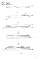
Fig. 1 has shown the technology of preparation creep resistance metal.
Fig. 2 (a) be have ion implanted region stacked conducting plate schematic cross-section.
Fig. 2 (b) is the synoptic diagram of the Fig. 2 (a) behind the recrystallize.
Fig. 3 is through injecting the TEM(photo in the cross section, crystal boundary area after handling), in this zone, formed a series of vesicles, stop the growth of crystal boundary.
Fig. 4 has shown that the potassium along the dislocation growth steeps in the upper layer of tungsten.
Fig. 5 (a) showed ion implantation during operable geometric decomposition diagram.
What Fig. 5 (b) showed is the front view of Fig. 5 behind the recrystallize (a).
Fig. 6 (a) is the double-deck rubidium sectional view without ion implantation preparation.
Fig. 6 (b) is the sectional view of Fig. 6 (a) after 2000 ° of K annealing in four hours.
Fig. 6 (c) is the sectional view that injects the double-deck rubidium of preparation with potassium ion.
Fig. 6 (d) is the sectional view of Fig. 6 (c) after 2000 ° of K annealing in four hours.
Fig. 7 is at two hours the rubidium bilayer (structure) with the potassium ion injection of 1750 ℃ of recrystallize.
Referring now to Fig. 1, at this method of the metal or alloy of Implantation atom that a kind of formation distributes with disperse or adulterant is disclosed. Especially disclose a kind of internal high temperature barrier layer that in the structural metal, forms preventing crystal boundary and dislocation motion, thereby made said structural metal under high relative temperature, have the method for creep resistant. The method comprises provides the ground floor that is made of structural metal or carrier metal, this metalloid is tending towards creep under high relative temperature, and be zero or very low to the solubility of lower column element, these elements are xenon, argon, neon, helium, krypton, potassium, rubidium, caesium, francium or its mixture. Available metal is listed in the table 1.
Still with reference to Fig. 1, the ground floor that is made of metal 10 is doped, and injects or be filled with ion 12 to form injection region 14, and wherein, this ion comprises inertia (rare) element xenon, helium, argon, krypton, neon or alkali metal potassium, rubidium, caesium, francium, or its mixture. By direct or indirect method these ions are inserted in ground floors, said method comprise Implantation, Recoil injection or Ion Mixing etc.
Through the first metal layer of Implantation deposition or the second structural metal layer 16 that superposes to form laminated product or composition 18. Available chemistry or physical vapour deposition (PVD), plating, thermal spray deposition, electro-deposition, sputtering sedimentation, pressure knot or other method are carried out lamination operation or the second structural metal layer are provided.
The step of injection and the stack second layer can be at random repeatedly to form sandwich construction. Although in forming the layered article process, apply the normally last step of second metal level, also can apply any a plurality of layer. As an example, Fig. 1 has shown three overall condition that metal level is carried two ion implanted regions secretly. The alloy of table I disclosed metal can form by the method that the vapor phase of each element is mixed, and the operation that perhaps adds layer or deposited monolayers (its can by postorder heat treatment homogenising) by hocketing prepares.
Stacking or arranged enough several target zones after just obtain the sheet metal 18 processed through interior doping or Implantation. Element through Implantation is insoluble in the structural metal basically, nor diffuses through easily the structural metal sheet, even if at high temperature. Therefore, this can be used to make filament sample, heat shielding cover, the propulsion tube of resistojet, turbine, or as other purposes.
Above (with the table III) listed inert element have the littler atomic volume of alkali metal than above-mentioned (with the table II), and compare with the structural metal and not quite. The high-temperature stability of inert gas bubbles and different listed alkali-metal high-temperature stability are equally big. Yet the inert gas bubbles that forms in metal can play the effect of pinning dislocation really.
Fig. 2 (a) is the schematic cross-section of multilayered metal film. Every all is relative fine grained textures' (cylindrulite), and all through Implantation, has fine element district 14, and this element is from showing in the listed group of II and table III. Intrametallic columnar grain 30 can obviously be seen in the figure.
Metal level after heat treatment, recrystallize takes place in it.Shown in Fig. 2 (b), crystal boundary 30 alligatoring, and blocked at ion implanted region 14.And lamellated crystalline-granular texture produced, that is Yin Wendu raises and produces long crystal boundary and stoped by ion implanted region 14, makes it fully to expand the whole thickness that passes metal level.
Fig. 3 is the cross section Photomicrograph that the potassium of rubidium bilayer (sheet) injects the crystal boundary area.Annealed four hours under 2000 ° of K through injecting the metal of handling, can see because numerous bubbles that high temperature caused.The tungsten that Fig. 4 also demonstrates the potassium injection similarly has the formation of tiny potassium bubble 2200 ℃ of annealing one hour and 2300 ℃ of annealing after 30 minutes.The growth of bubble shows as along obviously dislocation growth, and near free surface.The partly cause of bubble growth is the inflow and the absorption in room.Bubble is tending towards pinning or stops crystal boundary and dislocation motion to pass whole metal.
The geometrical shape of each layer of structural metal can change.These layers are flat, crooked, shaft-like, octagonal shape or the like.Unique restriction for shape is from such fact, and promptly method for implanting requires in emission of ions mechanism and be injected into to have a direct light path between the surface.
Not only each of structural metal layer shape can change, and injection period, used geometricdrawing also can change.Fig. 5 (a) shows the graphic example that can use when ion implantation.Wherein, speckle regions 50 indicates the ion implantation element district in the multilayered metal film.Fig. 5 (b) has shown the structure of the Fig. 5 (a) after the recrystallize thermal treatment.Metal grain 52 alligatoring, and form a kind of grain boundary structure of commissure, perhaps forming the crystal grain layer that has spike dowel 54, spike dowel 54 inserts adjacent layerss by injecting barrier layer gap 56.This is in order to contrast with Fig. 2 (b), and in Fig. 2 (b), the injection region of each metal level all is complete surface.
Ion implantation or the Ion Mixing method of the element in table II and the III (as follows) has guaranteed that in doped layer it is that mode with the atomic state fine distribution is incorporated in the metal lattice.Ion is once be injected into, and they are electron gain once more just, and becomes stable element once more.But change ion implantation or blended parameter regulating course width and dopant dose.In material, doped layer is the sheet district.The obstacle that on behalf of highdensity prevention dislocation or crystal boundary, they move.Owing to alkali metal atom is difficult for greatly moving, people can infer that these obstacles at high temperature are quite stables, are difficult for alligatoring.If some limited alkali metal atoms at high temperature transmit, then can form the doping vesicle, as shown in Fig. 3 and Fig. 4 (potassium injects rubidium and potassium injects tungsten).Known in tungsten filament have such bubble to form.As long as these steep not alligatoring, the obstructive action of doping agent just can keep for a long time, and thus, creep resistance also can be kept for a long time.
The representative of element that following table is listed has also constituted most of important techniques structural metal and alloy, has pointed out their atomic volume or size, temperature of fusion and to the solubleness of doped element potassium, caesium, rubidium and francium simultaneously in the table
The table I
The structural metal, its atomic volume, temperature of fusion and to the solubleness of alkali metal element K, Rb, Cs, Fr
Former daughter fusing temperature
Long-pending<1〉cm
3Solubleness to alkali metal
Element/grammeatom degree<2〉℃ K Rb Cs Fr
Be 4.9 1,277 1, but exist
Compound is arranged
KBe
2〈4〉
Mg 14.0 650 0〈6〉 0〈6〉 0〈6〉
0〈3〉
Al 10.0 660 0<3〉0<3〉is very little
〈3)
Ti 10.7 1688 is very little
〈3〉
Continuous table I
K Rb Cs Fr
V 8.9 1900
Cr 7.3 1875
Mn 7.5 1245
Fe 7.1 1537 0<3> 0<3> 0<3>
Co 6.7 1495 -<3>
Ni 6.7 1453 -<5>
Cu 7.1 1083
Zn 9.2 420 KZ
r13<3>
Y 19.5 1509
Zr 14.0 1852 very little<6 〉
Nb 11.0 2415 0<5>
Mo 9.4 2610 is very little
*-<5 〉
Tc - 2200
Ru 8.3 2500
Rh 8.4 1966
Pd 9.3 1552
Ag 10.3 961
Hf 14.0 2222 0<6>
Ta 11.2 2996 -<6>
W 9.6 3410 is very little
*
Re 8.8 3180
Os 8.5 2700
Continuous table I
K Rb Cs Fr
Ir 8.6 2454
Rt 9.1 1769 -<3>
Au 10.2 1063 0<4> 0<4> 0<4>
But exist several but exist several but exist
Plant chemical combination species compd A uCs compound
The rare earth element atomic volume
La 22~24 920
Ce 21 804
Pr 21 919 very little<6 〉
Nd 21 1019
Pm - 1027
Sm 20 1072
Eu 20 826
Gd 20 1312
Tb 19 1356
Dy 19 1407
Ho - 1461
Er - 1497
Tm - 1545
Yb - 824
Lu - 1650
*. learn by system lamp industrial practice
One. do not point out solubleness in the document
1.N.F.Mott and H.Jones: " the performance principle of Metal and Alloy " Dover publishes, (1958), 318~319 pages.
2.W.G.Moffatt, G.W.Pearsall and J.Wulff: " performance of material and structure ", John Wiley and Sons, (1967), Vol.1,206,207 pages.
3.M.Hansen and K, Anderko: " structure of binary alloy ", McGraw-Hill(1958),
4.R.P.Elliott: " structure of binary alloy " first supplementary issue, McGraw-Hill, (1965)
5.F.A.Shunk: " structure of binary alloy " second supplementary issue, McGraw-Hill, (1969)
6.W.G.Moffatt: " binary phase diagram handbook ", General Electric Co., Schenectady, N.Y.(1978).
Following table II is to contrast with the table I.The table II comprises the atomic volume of element potassium, caesium, rubidium and francium.The size of most of atoms metals is smaller, and (grammeatom equals 6.02 * 10 to for example every grammeatom
23Individual atom) volume of shared tool is less than 15 cubic centimetres.Listed have only yttrium and rare earth element, from the lanthanum to the lutetium, has and reach 24 cubic centimetres of such large-sizes of every grammeatom.Both just like this, they compare with table II element be still little.
The table II
Be used for adulterated large size alkali metal
Be used for ion implantation element
The pantogen sub-volumes
1Temperature of fusion
2
Alkali metal cm
3/ grammeatom ℃
K 45.5 64
Rb 56.2 39
Cs 71.0 29
Fr (>70, estimated value) 27
1.N.F.Mott and H.Jones: " the performance principle of metal and alloy " Dover publishes, (1958), 318~319 pages.
2.W.G.Moffatt, G.W.Pearsall and J.Wulff: " performance of material and structure ", John Wiley and Sons the 1st volume (1967), 206,207 pages.
Compare with the atoms metal of table I, the large-size of table II atom has guaranteed their fixedly indiffusion in metal under high relative temperature.Relative temperature is defined as and is lower than temperature of fusion and the temperature after its temperature of fusion is proofreaied and correct.
Table II element forms stable small size bubble and improves creep resistance thus, and (this process) needed second prerequisite but they should not be dissolved in the metal lattice.Can see obviously that from the table I data of relevant solubleness are very rare.Estimation may be that described element only has very little in listed any metal or do not have solubleness because atomic size difference is big.The experimental data part is arranged, and solubleness is not zero to be exactly very little.
Can infer that the maximum likelihood of improving creep resistance will occur in the metal with maximum atomic size poor (group element such with comprising potassium, rubidium, caesium and francium compared).
The used example of mixing potassium tungsten and molybdenum shows that the improvement of creep resistance can be wished to betide in the metal of its atomic volume less than 10 cubic centimetres/grammeatom in the industry of system lamp.For their part, with alkali metal atom K, Rb, the size difference of Cs and Fr is very big.Concerning the metal such as Mg, Zr, Hf and rare earth metal of large-size, this size difference diminishes.Yet also can carry out doping treatment to it, particularly use sizable Rb, Cs or Fr atom doped.
The alkali metal that inert gas elements in the table III does not resemble in the table II is so big.Yet they in fact also are insoluble in the structural metal, and can form stable vesicle, and vesicle is pinning crystal boundary and dislocation conversely again.As long as tangible alligatoring does not at high temperature take place these bubbles, they just can provide the microstructure blocking layer to stop moving of crystal boundary and dislocation, thereby creep resistance is provided.
The table III
The zero group element
The solubleness of element in the solid-state structure metal
He is real
Matter
On the Ne
All
No
Ar is molten
In
The Kr knot
Structure
The Xe gold
Belong to
Free list II and one or more listed elements of table III mix.To mix the degree of depth all be should be by the parameter of optimal selection for doping content, ion implantation or ion in the repeat distance of doped layer, the layer.And ion implanted layer can be arranged by multiple geometricdrawing, forms commissure crystal grain during impelling recrystallize afterwards.It is minimum that the commissure crystalline-granular texture can reduce to the slip (a kind of form of creep) of crystal boundary.Many injection geometricdrawing all are suitable for, and Fig. 5 (a) has provided one and has been different from the example that whole plate injects.Yet, plan to indicate the figure of arranging of the best here.
Refer now to Fig. 6 (a)~Fig. 6 (d), it has provided the double-deck tangent plane fracture SEM of rubidium Photomicrograph.Fig. 6 (a) and 6(b) for the preparation that undopes, Fig. 6 (c) and 6(d) then comprise one deck potassium ion input horizon.
What show among the figure is a substrate.This substrate necessary base always not for the stepped construction metal, but here need be provided, because need deposit the first layer rubidium thereon with the method for chemical vapour deposition.Subsequently potassium ion is injected the first layer, deposition second layer rubidium on this ion implantation the first layer.Fig. 6 (a) and 6(b) showed and inject and the rubidium of preparation with potassium ion, Fig. 6 (c) and 6(d) performance be the rubidium of preparation of mixing.
Further, 6(a) and 6(c) showed the element of deposition attitude, and 6(b) and 6(d) represented the situation of same element after 2000K recrystallize and annealing.The barrier-layer effect of ion implanted layer is high-visible in Fig. 6 (d).Behind the recrystallize, the crystal boundary that Fig. 6 (b) shows has moved through the whole height of rubidium bilayer.In contrast, the crystal grain among Fig. 6 (d) is only gone to the potassium blocking layer.
Because grain boundary has only moved a percentage ratio (this is because the result that the potassium layer causes) of whole rubidium layer distance, be not difficult to learn therefore that potassium mixes and caused creep resisting stability, makes crystalline-granular texture be the crossover shape.
With reference to Fig. 7, potassium ion is injected in the rubidium layer of chemical vapor deposition (CVD) formation, dosage is 1 * 10
16, 1 * 10
17With 3 * 10
17Ion/cm
2, 150eV, vapour deposition adds the rubidium layer again on input horizon.In 1750 ℃ of recrystallize after two hours, the rubidium grain-size is by growing up to above 100 microns less than 20 microns.Yet grain boundary maintains the place of ion implantation potassium layer, thereby has prevented that grain boundary from wearing the whole width that moves past the rubidium sheet.In contrast, the double-deck rubidium of the CVD that no potassium injects is when recrystallize, and the recrystal grain boundary moves through the whole width of rubidium layer, forms the columnar microstructure of no crossover crystal grain, and this structure is considered at high temperature to produce inferior creep resistance.
Described technology can be used to prepare wire, band shape or tubulose filament.One suitable matrix is provided, and for example molybdenum deposits the thick tungsten layer of a few micron number magnitudes thereon with chemical vapour deposition or physical gas-phase deposite method.Use ion implantation tungsten layer then, inject the degree of depth and reach 0.1 micron the order of magnitude.This has just made ion implantation blocking layer.With chemical vapour deposition or physical gas-phase deposite method deposition second layer tungsten, thickness still is a few micron number magnitudes then.Additional ion implanted layer and tungsten deposition can be repeated repeatedly, also can finish this technology behind deposition second layer tungsten layer.
With compacting, method rolling or punching press filament is shaped then.The processing Ying Yu that is shaped is higher than under 600 ℃ the temperature and carries out, to prevent brittle rupture.Viscous deformation to a certain degree needs, because it can provide the motivating force that makes the crystal grain edge be parallel to blocking layer direction growth in filament annealing or during firing.Can obtain a kind of extended crossover crystalline-granular texture according to the method, it can improve the creep resistance of filament material.The high-temperature stability of internal barriers has guaranteed the stability of this crystal grain crossover structure during burn-out life.
Then, with the method that is similar to known standard winding shape filament filament is annealed.Anneal has been fixed filament shape, and prevents from when the postorder matrix is removed to produce bullet behind the over-drastic.
With being similar to the currently known methods that twines in the processing of shape filament removal is corroded in the molybdenum substrate.Clamp according to the tail end of known standard method, so that conduction current ribbon filament.Subsequently, with known standard method filament is placed in the lamp housing.
The short annealing device is to be used to that silicon chip is carried out short-term annealing (a few second) handle, so that lattice defect obtains healing (eliminations), the diffusion of doping agent is distributed again keep minimum.The growth of the sull on the silicon also can be another purpose of short annealing.On the whole silicon wafer area, need excellent temperature steady, usually will be with tungsten line filament arrange to the entire working surface radiation heating.For on relatively large zone (10
11* 10
11The order of magnitude) carry out even heating, ribbon filament is then more favourable.
The technology of preparation heating zone is similar to the technology of embodiment 1 described preparation ribbon filament.The concise and to the point main points of preparation molybdenum band are:
1. obtain the molybdenum foil that approaches earlier, for example through rolling or vapour deposition is made, its surface should be clean, does not promptly have scale or dirt.
2. inject the blocking layer to the molybdenum surface ion, input horizon comprises in K, Rb, Cs, the Fr group or inert element He, Ne, Ar, Xe, Kr group in a kind of element.Injecting depth range is about 1~1000nm, and the scope of implantation dosage is about 10
13* 10
17/ cm
2, optimal dose depends on the selected injection degree of depth.Increase with the desired degree of depth, dosage also should increase.Lower dosage is 10
13About the order of magnitude, be to be used in shallow injection, promptly inject the degree of depth and be approximately 10nm.Higher dosage is to be used for darker injection, that is about 1 micron degree of depth.The typical peak concentration of input horizon (promptly the highest at this deep ion implantation concentration) serves as that contrast is 0.01%~5% injection atom (atomic percent) with atom on every side.
3. second layer molybdenum is deposited on the ion implantation molybdenum layer, and the blocking layer is covered in the laminated tape structure.Step 2 and step 3 can be repeated to carry out.
4. make the laminated tape distortion then, for example, it is thinned to desired thickness, or make it become desired heating zone shape by punching press, cutting or crooked method with the method for rolling.
Embodiment 3 thermoshield covers
The thermoshield cover is to be used for vacuum oven, rocket and aeroengine, high-temperature plasma constrainer, nuclear reactor and other field.
The thermoshield cover is normally made by heating resisting metal or alloy sheets, and is the state of going along with sb. to guard him to make special applications.That describe below is the preparation method with the heat shield plate on interior high temperature blocking layer.
1. provide needed alloy slice or plate, for example Mo-0.5%Ti-0.1%Zr alloy slice or plate.The surface must cleaning (oxide compound or other scale must be removed).
2. inject the blocking layer to surface ion, the blocking layer comprises in K, Rb, Cs, the Fr group or inert element He, Ne, Ar, Kr, Xe group in a kind of element.The scope of injecting the degree of depth is about 1~1000nm.The scope of implantation dosage is about 10
13~10
17/ cm
2, optimal dose depends on the selected injection degree of depth.Can on whole surface, inject continuously, perhaps inject, so that when the recrystallize of end product is handled, produce the crossover grain microstructure in the mode of figure.And by chance the spike dowel phenomenon is arranged, promptly in the place that lacks the blocking layer, grain growing enters adjacent layer.
3. two or more injection sheets are stacked each other with the form layers stack structure.Then this stepped construction is encapsulated in (sheath material will be removed afterwards) in the evacuated jacket.
With stepped construction under the condition of high temperature and pressurization, as hot isostatic pressing, together through diffusion-bonded.
5. with this structure hot rolling or forge into desired thickness and shape.Remove sheath material with etching method.
The propulsion tube of embodiment 4 resistojets
Resistojet is to be used for the location of man-made satellite or space equipment or the device of rotation.This device is usually less and produce the thrust of a few gram orders of magnitude.Thrust is to be produced by the injection of gaseous matter, for example the injection of hydrogen or ammonia.Spray required pressure by in resistive heating chamber and thrust tube, heating to produce.Obtain good thrust efficiency, high temperature is essential.This has just required high temperature creep-resisting and thermal shock resistance concerning the structural metal.For this purpose, rhenium or W-Re alloys are good selected objects.What describe below is how to use the method for burying ion implantation blocking layer to constitute creep resistance thrust (advancing) pipe.
1. the rhenium of several micron thickness is deposited upon garden cylindricality matrix for example on the garden side face of molybdenum core bar, this core bar will be removed later.The method that is suitable for forming this layer is a chemical Vapor deposition process.
2. will be ion implantation in the rhenium surface by in K, Rb, Cs, the Fr group or the formed blocking layer of a kind of element in inert element He, Ne, Ar, Kr, the Xe group.Cylinder should rotate in ionic fluid, carries out so that be infused on the side face of whole garden.Injecting depth range is about 1~1000nm.The implantation dosage scope is about 10
13~10
17/ cm
2, optimal dose depends on the selected injection degree of depth.Injection can be carried out on whole surface continuously, perhaps carries out in a kind of mode of figure, so that finished product can produce the crossover grain microstructure when recrystallize is handled, and the spike dowel phenomenon is arranged by chance, and promptly in the zone that lacks the blocking layer, grain growing enters in the adjacent layers.
3. as the first step, deposit second layer rhenium, the blocking layer is covered.Second and third step can repeat.
4. the synthetic Cylinder is made desired diameter through mold pressing, drawing or forging.
5. remove the molybdenum core bar with the selection etching method, the rhenium pipe that stays has interior ring-type blocking layer, and this layer will guide grain growing when the high temperature recrystallize, makes it to form creep resisting crossover crystalline-granular texture.This structure improves the use temperature in resistojet becomes possibility.
The principal direction of stress that produces owing to centrifugal force is the long axis direction along turbine blade, is undesirable perpendicular to the grain boundary of this stress axis, because they can become the position that fracture is sprouted in the hot operation process.And the grain boundary that is parallel to stress axis does not play deleterious effect.For obtaining this microstructure state, the nickel base superalloy turbine blade is carried out the directional freeze operation.
The single crystal blade that crystal boundary all is eliminated can be grown.Along the blades axes direction and have the growth of column crystal structure of good habit or the growth of zero defect single crystal blade all owing to the increase of vane thickness becomes more difficult.But thin slice can be grown more perfectly.
Having described a kind of how the use at this buries ion implantation blocking layer to produce crystal boundary is to not or the method for the crossover crystal grain recrystallization texture of rare horizontal crystal boundary substantially along blades axes.
1. use that a kind of to have certain thickness this thickness of superalloy sheet be the part of needed turbine blade thickness.Polycrystalline or single-chip all can use.The surface must be clean.
2. the ion implantation surface of advancing the superalloy sheet, the blocking layer that will be made of a kind of element in the following group, said group comprises K, Rb, Cs, Fr or inert element He, Ne, Ar, Kr, Xe.Injecting depth range is about 1~1000nm.The implantation dosage scope is about 10
13~10
17/ cm
2, optimal dose depends on the selected injection degree of depth.Can inject continuously on whole surface, mode that also can a kind of figure is injected, so that end product produces the crossover grain microstructure when recrystallize, and idol has the spike dowel phenomenon, promptly lacking the place, blocking layer, and grain growing is advanced in the adjacent layers.
3. two or more injection sheets are stacked together mutually, form rhythmo structure.The profile of these sheets should be disposed near the shape of needed turbine blade.
4. this laminated product is packaged in (sheath material will be removed afterwards) in the evacuated jacket, and under high temperature and pressurized conditions,, this goods diffusion is linked together as hot isostatic pressing.
5. remove sheath material, for example use etching method.
6. blade is made suitable size with machining.
7. blade is carried out recrystallize and handles, preferably by one along blades axes to temperature gradient field.The blocking layer of burying will guide grain growing, with produce along blades axes to the laminated die structure.The place that is disconnected wittingly on the blocking layer only is because the crystal grain spike dowel inserts adjacent layers, so can produce horizontal crystal boundary.
The invention has been described by preferred embodiment.Obviously, to those readings and after having understood above-mentioned specification sheets other people improve and conversion all can occur.We wish that the present invention should be interpreted into and comprise all these conversion and modification because they be within the scope of the claim of carrying or its equivalent.
Claims (7)
- Make said structural metal produce the method for creep resistance thereby 1, form the internal high temperature blocking layer in the structural metal under high relative temperature to prevent crystal boundary and dislocation moving, this method comprises the steps:The first layer structural metal is provided, and said structural metal type is to be tending towards creep under high relative temperature, and to have zero or low solubleness by the element set that xenon, helium, neon, argon, krypton, potassium, rubidium, caesium and francium constituted;Inject ion and form the injection region in said the first layer metal, said ion is the member in the group that is made of element xenon, helium, neon, argon, krypton, potassium, rubidium, caesium, francium and composition thereof; AndAdd the second structural metal layer and form mixture on first ion implanted layer, cover in mixture the injection region.
- 2, according to the process of claim 1 wherein, can provide said the first layer with multiple geometrical shape, for example plane or on curved surface elements, finish ion implantation step along clear path whereby.
- 3, according to the process of claim 1 wherein that the step that applies the second structural metal layer can be finished with following method: vapour deposition, plating, thermal spray deposition, galvanic deposit, sputtering sedimentation or pressure combination.
- 4, according to the process of claim 1 wherein that the structural metal that is tending towards creep under high relative temperature is a member in following group: Be, Mg, Al, Ti, V, Cr, Mn, Fe, Co, Ni, Cu, Zn, Y, Zr, Nb, Mo, Tc, Ru, Rh, Pd, Ag, Ln, Hf, Ta, W, Re, Os, Ir, Pt, Au, La, Ce, Pr, Nd, Pm, Sm, Eu, Gd, Tb, Dy, Ho, Er, Tm, Yb and alloy thereof.
- 5, according to the method for claim 1, wherein ion implantation atom can the sheet district the form disperse be distributed in the first structural metal floor, and in these districts, form rill with the moving of pinning dislocation and crystal boundary, stop creep to reach recrystallize on desired directions not thus.
- 6, repeat according to the process of claim 1 wherein to inject and add a layer step.
- 7, according to the formed mixture of the method for claim 1.
Applications Claiming Priority (2)
| Application Number | Priority Date | Filing Date | Title |
|---|---|---|---|
| US07/232,284 US4915746A (en) | 1988-08-15 | 1988-08-15 | Method of forming high temperature barriers in structural metals to make such metals creep resistant at high homologous temperatures |
| US232,284 | 1988-08-15 |
Publications (2)
| Publication Number | Publication Date |
|---|---|
| CN1041009A CN1041009A (en) | 1990-04-04 |
| CN1020239C true CN1020239C (en) | 1993-04-07 |
Family
ID=22872534
Family Applications (1)
| Application Number | Title | Priority Date | Filing Date |
|---|---|---|---|
| CN89107597A Expired - Fee Related CN1020239C (en) | 1988-08-15 | 1989-08-15 | Method of forming high temp. barriers in structural metals to make such metals creep resistant at high homologous temp. |
Country Status (6)
| Country | Link |
|---|---|
| US (1) | US4915746A (en) |
| EP (1) | EP0356111B1 (en) |
| JP (1) | JP2930327B2 (en) |
| CN (1) | CN1020239C (en) |
| AT (1) | ATE95845T1 (en) |
| DE (1) | DE68909865T2 (en) |
Families Citing this family (34)
| Publication number | Priority date | Publication date | Assignee | Title |
|---|---|---|---|---|
| JP2823276B2 (en) * | 1989-03-18 | 1998-11-11 | 株式会社東芝 | Method for manufacturing X-ray mask and apparatus for controlling internal stress of thin film |
| WO1990014670A1 (en) * | 1989-05-02 | 1990-11-29 | Electric Power Research Institute, Inc. | Isotope deposition, stimulation, and direct energy conversion for nuclear fusion in a solid |
| US5288561A (en) * | 1990-10-30 | 1994-02-22 | Kabushiki Kaisha Toshiba | High temperature heat-treating jig |
| FR2672829B1 (en) * | 1991-02-19 | 1995-06-30 | Nitruvid | METHOD FOR REALIZING A BRAZING LINK BETWEEN TWO PIECES, IN PARTICULAR A CERAMIC PIECE AND A METAL PIECE, AND WELDED ASSEMBLY PRODUCED BY THIS PROCESS. |
| US5248130A (en) * | 1991-03-11 | 1993-09-28 | Eaton Corporation | Vehicle leaf spring with irradiated center for crack diversion |
| AT398580B (en) * | 1991-11-05 | 1994-12-27 | Strauss Helmut | COATING FOR METAL OR NON-METAL SUBSTRATES, METHOD AND DEVICE FOR THE PRODUCTION THEREOF |
| US5298095A (en) * | 1991-12-20 | 1994-03-29 | Rmi Titanium Company | Enhancement of hot workability of titanium base alloy by use of thermal spray coatings |
| US5543348A (en) * | 1995-03-29 | 1996-08-06 | Kabushiki Kaisha Toshiba | Controlled recrystallization of buried strap in a semiconductor memory device |
| US5556713A (en) * | 1995-04-06 | 1996-09-17 | Southwest Research Institute | Diffusion barrier for protective coatings |
| US5905279A (en) * | 1996-04-09 | 1999-05-18 | Kabushiki Kaisha Toshiba | Low resistant trench fill for a semiconductor device |
| US5885896A (en) * | 1996-07-08 | 1999-03-23 | Micron Technology, Inc. | Using implants to lower anneal temperatures |
| US6083567A (en) * | 1996-08-30 | 2000-07-04 | University Of Maryland, Baltimore County | Sequential ion implantation and deposition (SIID) technique |
| US5763017A (en) * | 1996-10-28 | 1998-06-09 | Toyo Technologies Inc. | Method for producing micro-bubble-textured material |
| US6098655A (en) * | 1996-12-03 | 2000-08-08 | Carolina Power & Light Company | Alleviating sticking of normally closed valves in nuclear reactor plants |
| US6063246A (en) * | 1997-05-23 | 2000-05-16 | University Of Houston | Method for depositing a carbon film on a membrane |
| US6143141A (en) * | 1997-09-12 | 2000-11-07 | Southwest Research Institute | Method of forming a diffusion barrier for overlay coatings |
| US6188134B1 (en) * | 1998-08-20 | 2001-02-13 | The United States Of America As Represented By The Secretary Of The Navy | Electronic devices with rubidium barrier film and process for making same |
| US6351036B1 (en) | 1998-08-20 | 2002-02-26 | The United States Of America As Represented By The Secretary Of The Navy | Electronic devices with a barrier film and process for making same |
| WO2001061067A1 (en) * | 2000-02-17 | 2001-08-23 | Anatoly Nikolaevich Paderov | Combined protective coating of parts made of heat resisting alloys |
| US7229675B1 (en) | 2000-02-17 | 2007-06-12 | Anatoly Nikolaevich Paderov | Protective coating method for pieces made of heat resistant alloys |
| US6465887B1 (en) | 2000-05-03 | 2002-10-15 | The United States Of America As Represented By The Secretary Of The Navy | Electronic devices with diffusion barrier and process for making same |
| US9566148B2 (en) * | 2000-05-12 | 2017-02-14 | Vactronix Scientific, Inc. | Self-supporting laminated films, structural materials and medical devices manufactured therefrom and methods of making same |
| US6593227B1 (en) * | 2001-05-08 | 2003-07-15 | Advanced Micro Devices, Inc. | Method and apparatus for planarizing surfaces of semiconductor device conductive layers |
| EP1946796A3 (en) * | 2001-12-12 | 2009-03-11 | The Univ. of Alberta, The Univ. of British Columbia, Carleton Univ., Simon Fraser Univ. and The Univ. of Victoria | Radioactive ion |
| ATE395100T1 (en) * | 2001-12-12 | 2008-05-15 | Univ Of Alberta The Univ Of Br | RADIOACTIVE ION |
| DE102004051374A1 (en) * | 2003-10-30 | 2005-06-02 | Sumitomo Electric Industries, Ltd. | Electroformed ion implantation structural material and method of making the structural material |
| GB2450933A (en) * | 2007-07-13 | 2009-01-14 | Hauzer Techno Coating Bv | Method of providing a hard coating |
| CN102582156A (en) * | 2012-02-10 | 2012-07-18 | 王宝根 | Production line for hypersonic flame aluminium powder fusion iron composite boards |
| CN103921498B (en) * | 2013-01-15 | 2017-08-29 | 深圳富泰宏精密工业有限公司 | Stainless steel products with hard film layer and preparation method thereof |
| CN104342627B (en) * | 2014-09-25 | 2016-12-07 | 昆明理工大学 | A kind of pure copper material method for surface hardening |
| CN105543797A (en) * | 2015-12-12 | 2016-05-04 | 朱惠冲 | Manufacturing process of rhenium-lanthanum rare-earth alloy high-energy electronic injection target |
| US10017844B2 (en) | 2015-12-18 | 2018-07-10 | General Electric Company | Coated articles and method for making |
| CN107385404A (en) * | 2017-06-28 | 2017-11-24 | 江苏大学 | A kind of process that nickel-base alloy surface hardness is improved using He isotopic geochemistry |
| CN114262912B (en) * | 2020-10-16 | 2024-03-15 | 天津大学 | IrNi nanoparticles with dislocation-strain effect |
Family Cites Families (17)
| Publication number | Priority date | Publication date | Assignee | Title |
|---|---|---|---|---|
| US3900636A (en) * | 1971-01-21 | 1975-08-19 | Gillette Co | Method of treating cutting edges |
| IL38468A (en) * | 1971-02-02 | 1974-11-29 | Hughes Aircraft Co | Electrical resistance device and its production |
| US3806380A (en) * | 1971-03-05 | 1974-04-23 | Hitachi Ltd | Method for hardening treatment of aluminum or aluminum-base alloy |
| GB1392811A (en) * | 1971-04-07 | 1975-04-30 | Atomic Energy Authority Uk | Methods for treating steel to modify the structure thereof |
| US3811936A (en) * | 1971-12-22 | 1974-05-21 | Westinghouse Electric Corp | Method for producing refractory metal members by vapor deposition,and resulting product |
| CA1028935A (en) * | 1973-12-14 | 1978-04-04 | Niels N. Engel | Superhard martensite and method of making same |
| GB1555802A (en) * | 1976-01-28 | 1979-11-14 | Atomic Energy Authority Uk | Metalworking tool elements |
| US4123833A (en) * | 1977-10-13 | 1978-11-07 | Westinghouse Electric Corp. | Method of producing doped tungsten filaments by ion-implantation |
| US4296352A (en) * | 1979-12-19 | 1981-10-20 | General Electric Company | Incandescent lamp |
| US4433005A (en) * | 1980-05-05 | 1984-02-21 | United Technologies Corporation | Fatigue resistant tatanium alloy articles |
| JPS5739152A (en) * | 1980-08-18 | 1982-03-04 | Matsushita Electronics Corp | Tungsten material for light bulb |
| US4372985A (en) * | 1980-12-08 | 1983-02-08 | Rockwell International Corporation | Ion implantation for hard bubble suppression |
| JPS57186285A (en) * | 1981-05-11 | 1982-11-16 | Hitachi Ltd | Manufacture of magnetic bubble memory element |
| JPS57186284A (en) * | 1981-05-11 | 1982-11-16 | Hitachi Ltd | Manufacture of magnetic bubble memory element |
| US4542009A (en) * | 1983-04-21 | 1985-09-17 | Combustion Engineering, Inc. | Synthesis of intercalatable layered stable transition metal chalcogenides and alkali metal-transition metal chalcogenides |
| US4520040A (en) * | 1983-12-15 | 1985-05-28 | Varian Associates, Inc. | Ferromagnetic films for high density recording and methods of production |
| US4743308A (en) * | 1987-01-20 | 1988-05-10 | Spire Corporation | Corrosion inhibition of metal alloys |
-
1988
- 1988-08-15 US US07/232,284 patent/US4915746A/en not_active Expired - Fee Related
-
1989
- 1989-08-15 AT AT89308265T patent/ATE95845T1/en not_active IP Right Cessation
- 1989-08-15 JP JP1210568A patent/JP2930327B2/en not_active Expired - Lifetime
- 1989-08-15 DE DE89308265T patent/DE68909865T2/en not_active Expired - Fee Related
- 1989-08-15 EP EP89308265A patent/EP0356111B1/en not_active Expired - Lifetime
- 1989-08-15 CN CN89107597A patent/CN1020239C/en not_active Expired - Fee Related
Also Published As
| Publication number | Publication date |
|---|---|
| JPH0320455A (en) | 1991-01-29 |
| EP0356111B1 (en) | 1993-10-13 |
| ATE95845T1 (en) | 1993-10-15 |
| EP0356111A1 (en) | 1990-02-28 |
| DE68909865D1 (en) | 1993-11-18 |
| DE68909865T2 (en) | 1994-05-11 |
| US4915746A (en) | 1990-04-10 |
| CN1041009A (en) | 1990-04-04 |
| JP2930327B2 (en) | 1999-08-03 |
Similar Documents
| Publication | Publication Date | Title |
|---|---|---|
| CN1020239C (en) | Method of forming high temp. barriers in structural metals to make such metals creep resistant at high homologous temp. | |
| JP5408827B2 (en) | Erosion resistant yttrium-containing metal with oxide film for plasma chamber components | |
| US9767983B2 (en) | Rotary X-ray anode and production method | |
| EP2461379B1 (en) | Wafer for led mounting, method for manufacturing the same, and led-mounted structure using the wafer | |
| EP2784173B1 (en) | Sputtering target and method for producing same | |
| EP2607507B1 (en) | High-strength titanium alloy member and process for production thereof | |
| JP2010248619A (en) | Method for producing oxygen-containing copper alloy film | |
| EP2518179A1 (en) | Gadolinium sputtering target and method for manufacturing the target | |
| CN115461502A (en) | Base substrate for III-V group compound crystal and method for producing same | |
| JP2024051069A (en) | Gallium nitride-based sintered body and manufacturing method thereof | |
| JP6144858B1 (en) | Oxide sintered body, sputtering target, and production method thereof | |
| JP5672252B2 (en) | Cu-Ga sputtering target and manufacturing method thereof | |
| EP3637484A1 (en) | Semiconductor substrate and method for producing same, substrate, and laminate | |
| JP6007840B2 (en) | Cu-Ga sputtering target and manufacturing method thereof | |
| JP6502399B2 (en) | Single crystal silicon sputtering target | |
| TW201715581A (en) | Paste composition and method for forming silicon germanium layer | |
| KR20210071954A (en) | Gallium nitride-based sintered compact and method for manufacturing the same | |
| RU2451766C1 (en) | Method for biaxial textured substrate production from binary alloy on basis of nickel for epitaxial application of buffer and high-temperature superconductive layers for ribbon superconductors to substrate | |
| CN103250234A (en) | Process for annealing semiconductor wafers with flat dopant depth profiles | |
| JP7500941B2 (en) | Gallium nitride sintered body and method for producing same | |
| JPH1161392A (en) | Production of sputtering target for forming ru thin film | |
| JPH09108908A (en) | Cermet-made cutting tool excellent in defect resistance | |
| JP2019073804A (en) | Single crystal silicon sputtering target | |
| TWI433953B (en) | Sputtering titanium target | |
| Shimoda et al. | Surfactant-mediated growth of epitaxial films on quasiperiodic surfaces |
Legal Events
| Date | Code | Title | Description |
|---|---|---|---|
| C06 | Publication | ||
| PB01 | Publication | ||
| C10 | Entry into substantive examination | ||
| C10 | Entry into substantive examination | ||
| SE01 | Entry into force of request for substantive examination | ||
| C14 | Grant of patent or utility model | ||
| GR01 | Patent grant | ||
| C19 | Lapse of patent right due to non-payment of the annual fee | ||
| CF01 | Termination of patent right due to non-payment of annual fee |