CN102004273A - Optical element and method for manufacturing optical element - Google Patents
Optical element and method for manufacturing optical element Download PDFInfo
- Publication number
- CN102004273A CN102004273A CN2010102720526A CN201010272052A CN102004273A CN 102004273 A CN102004273 A CN 102004273A CN 2010102720526 A CN2010102720526 A CN 2010102720526A CN 201010272052 A CN201010272052 A CN 201010272052A CN 102004273 A CN102004273 A CN 102004273A
- Authority
- CN
- China
- Prior art keywords
- tectosome
- optical element
- equal
- matrix
- track
- Prior art date
- Legal status (The legal status is an assumption and is not a legal conclusion. Google has not performed a legal analysis and makes no representation as to the accuracy of the status listed.)
- Pending
Links
Images


Classifications
-
- G—PHYSICS
- G02—OPTICS
- G02B—OPTICAL ELEMENTS, SYSTEMS OR APPARATUS
- G02B1/00—Optical elements characterised by the material of which they are made; Optical coatings for optical elements
- G02B1/10—Optical coatings produced by application to, or surface treatment of, optical elements
- G02B1/11—Anti-reflection coatings
- G02B1/118—Anti-reflection coatings having sub-optical wavelength surface structures designed to provide an enhanced transmittance, e.g. moth-eye structures
-
- G—PHYSICS
- G02—OPTICS
- G02B—OPTICAL ELEMENTS, SYSTEMS OR APPARATUS
- G02B1/00—Optical elements characterised by the material of which they are made; Optical coatings for optical elements
- G02B1/10—Optical coatings produced by application to, or surface treatment of, optical elements
- G02B1/18—Coatings for keeping optical surfaces clean, e.g. hydrophobic or photo-catalytic films
-
- G—PHYSICS
- G02—OPTICS
- G02B—OPTICAL ELEMENTS, SYSTEMS OR APPARATUS
- G02B27/00—Optical systems or apparatus not provided for by any of the groups G02B1/00 - G02B26/00, G02B30/00
- G02B27/0006—Optical systems or apparatus not provided for by any of the groups G02B1/00 - G02B26/00, G02B30/00 with means to keep optical surfaces clean, e.g. by preventing or removing dirt, stains, contamination, condensation
Landscapes
- Physics & Mathematics (AREA)
- General Physics & Mathematics (AREA)
- Optics & Photonics (AREA)
- Chemical & Material Sciences (AREA)
- Chemical Kinetics & Catalysis (AREA)
- Surface Treatment Of Optical Elements (AREA)
- Liquid Crystal (AREA)
- Optical Elements Other Than Lenses (AREA)
- Laminated Bodies (AREA)
Abstract
The invention provides an optical element and a method for manufacturing the optical element. The optical element with an antireflection function is provided with a substrate having a surface and a plurality of structures formed from convex portions or concave portions and arranged in large numbers on the surface of the substrate with a minute pitch less than or equal to the wavelength of the visible light, wherein the modulus of elasticity of the material forming the structures is 1 MPa or more, and 1,200 MPa or less, and the aspect ratio of the structure is 0.6 or more, and 1.5 or less.
Description
Technical field
The present invention relates to have the optical element and the manufacture method thereof of anti-reflective function.The a plurality of tectosomes that are specifically related to wherein be made of protuberance or recess dispose a plurality of optical elements and manufacture method thereof from the teeth outwards with the trickle pitch smaller or equal to wavelength of visible light.
Background technology
On the optical element that uses light-transmitting substrates such as glass, plastics, carry out surface treatment for the surface reflection that prevents light sometimes at present.As this surface treatment, form trickle and fine and close concavo-convex (moth eye) (for example with reference to non-patent literature 1) at optical element surface sometimes.
Generally be provided with under the situation of periodic concaveconvex shape at optical element surface, diffraction should take place during the place in light transmission, and the composition that directly advances that sees through light reduces significantly.But diffraction is not taking place than seeing through under the short situation of light wavelength in the pitch of concaveconvex shape, for example, when to make concaveconvex shape be rectangle described later, can effectively be prevented the effect that reflects to the light of the single wavelength corresponding with its pitch or the degree of depth etc.
As the moth eye tectosome that utilizes electron beam exposure to make, disclosed the moth eye tectosome (the about 300mm of pitch, the about 400mm of the degree of depth) (for example with reference to non-patent literature 2) of trickle tent like.It is high-performance preventing reflection characteristic below 1% that this moth eye tectosome can obtain reflectivity.
Moth eye tectosome as the method for the former dish manufacturing process of utilizing CD and etch process combination is made has disclosed the moth eye tectosome (for example referring to Patent Document 1) that hangs bell and oval frustum shape.This tectosome can obtain the preventing reflection characteristic near electron beam exposure.
Non-patent literature 1: with reference to " optical tech contact " Vol.43, No.11 (2005), 630-637
Non-patent literature 2:NTT Advanced Technology Co., Ltd., " the dependent antireflection object of no wavelength (moth eye) the former dish of mould ", [online], [putting down into retrieval on February 27th, 20], network
Patent documentation 1: the international separate edition that discloses No. 08/023816
Above-mentioned moth eye tectosome is owing to use by form the trickle concavo-convex principle that makes refractive index change inhibitory reflex on the surface interimly, if therefore fingerprint then preferably can be removed spot by xerotripsis attached on the tectosome.In case this is because the spots such as oily composition that contain in the fingerprint are filled up the recess of moth eye tectosome, then can not inhibitory reflex.
In case fingerprint is attached on the moth eye tectosome, then spot is adhered to according to the apperance of fingerprint, and stains attached is infiltrated the recess of tectosome by capillarity afterwards.If carry out xerotripsis under this state, spot is only filled up recess, so the reflection of concaveconvex shape suppresses the effect reduction, the reflectivity raising.
Utilize the material of low-surface-energies such as fluorine that coating is carried out on the surface, by can suppressing infiltration so a little, if but carry out xerotripsis then can not prevent infiltration to the tectosome recess to the tectosome recess.This is because the fiber finer that the recess of tectosome uses than xerotripsis, and the power that spot is retained in recess absorbs the power of spot greater than fiber.
Therefore, the optical element and the manufacture method thereof that the purpose of this invention is to provide spots such as erasable fingerprint.
Summary of the invention
In order to address the above problem, a first aspect of the present invention provides a kind of optical element with anti-reflective function, comprising: the matrix with surface; And with smaller or equal to the trickle pitch of wavelength of visible light in the surface configuration of described matrix a plurality of and a plurality of tectosomes that constitute by protuberance or recess, the elastic modulus of material that forms described tectosome more than or equal to 1MPa smaller or equal to 1200MPa, the depth-width ratio of described tectosome more than or equal to 0.6 smaller or equal to 1.5.
A second aspect of the present invention provides a kind of optical element with preventing reflection characteristic, comprise with a plurality of tectosomes a plurality of smaller or equal to the trickle pitch configuration of wavelength of visible light and that constitute by protuberance, the bottom of adjacent tectosome is engaged with each other, the elastic modulus of material that forms tectosome more than or equal to 1MPa smaller or equal to 1200MPa, the depth-width ratio of tectosome more than or equal to 0.6 smaller or equal to 1.5.
A third aspect of the present invention provides a kind of optical element with anti-reflective function, comprising: the matrix with surface; And with smaller or equal to the trickle pitch of wavelength of visible light in the surface configuration of described matrix a plurality of and a plurality of tectosomes that constitute by protuberance or recess, the elastic modulus of material that forms described tectosome more than or equal to 1MPa smaller or equal to 1200MPa, the depth-width ratio of described tectosome more than or equal to 0.6 smaller or equal to 5.
In the present invention, preferably main tectosome periodically is configured to quadrilateral clathrate or accurate quadrilateral clathrate.The quadrilateral grid here is the dimetric grid of making a comment or criticism.Accurate quadrilateral grid be meant the distortion different with just dimetric grid just dimetric grid.
For example, tectosome is configured under the situation on the straight line, accurate quadrilateral grid be instigate just dimetric grid to be gone up to stretch in linearity orientation (trajectory direction), the quadrilateral grid after the distortion.Under tectosome crawled the situation of arranging, accurate quadrilateral grid is meant by crawling of tectosome arranged the quadrilateral grid that makes after just dimetric grid is out of shape.Or instigate that just dimetric grid go up to stretch in linearity orientation (trajectory direction), distortion and arrange quadrilateral grid after the distortion by crawling of tectosome.
In the present invention, preferably tectosome periodically is configured to hexagonal grid or accurate hexagonal grid.The hexagonal grid here is meant the grid of regular hexagon.Accurate hexagonal grid be meant the distortion different with the grid of regular hexagon the grid of regular hexagon.
For example, tectosome is configured under the situation on the straight line, accurate hexagonal grid be instigate the grid of regular hexagon to be gone up to stretch in linearity orientation (trajectory direction), the hexagonal grid after the distortion.Tectosome crawls under the situation of arranging, and accurate hexagonal grid is meant by crawling of tectosome arranges hexagonal grid after the grid distortion that makes regular hexagon.Or the grid of instigating regular hexagon go up in linearity orientation (trajectory direction) stretch, distortion and arrange hexagonal grid after the distortion by crawling of tectosome.
In the present invention, ellipse is not only the oval completely of mathematical definition, also comprises the ellipse of distortion a little.Circle is not only circular (proper circle) completely of mathematical definition, also comprises the circle of distortion a little.
In the present invention, the configuration section of the tectosome in the preferred same track apart from P1 greater than the configuration section of the tectosome between two tracks of adjacency apart from P2.By like this, can improve the filling rate of tectosome with elliptic cone or oval frustum shape, therefore can improve preventing reflection characteristic.
In the present invention, each tectosome forms under the situation of hexagonal grid or accurate hexagonal grid at matrix surface, the configuration section of supposing the tectosome in the same track is apart from being P1, when the configuration section distance of the tectosome between two tracks of adjacency was P2, preferred proportion P1/P2 satisfied the relation of 1.00≤P1/P2≤1.1 or 1.00<P1/P2≤1.1.By being formed on this numerical range, can improving the filling rate of tectosome, therefore can improve preventing reflection characteristic with elliptic cone or oval frustum shape.
In the present invention, each tectosome forms at matrix surface under the situation of hexagonal grid or accurate hexagonal grid, preferably each tectosome elliptic cone or oval frustum shape that to be degree of tilt with long axis direction, central portion of bearing of trend at track form greater than the degree of tilt ground of top ends and bottom.By forming this shape, can improve preventing reflection characteristic and through performance.
In the present invention, each tectosome forms under the situation of hexagonal grid or accurate hexagonal grid at matrix surface, and the height of the tectosome of preferred trajectories bearing of trend or the degree of depth are less than the height or the degree of depth of the tectosome of the column direction of track.If do not satisfy such relation, must strengthen the configuration section distance of track bearing of trend, so the filling rate of the tectosome of track bearing of trend reduces.In case reducing, filling rate will cause reflection characteristic to reduce.
In the present invention, each tectosome forms at matrix surface under the situation of quadrilateral grid pattern or accurate quadrilateral grid pattern, the configuration section of the tectosome in the preferred same track apart from P1 greater than the configuration section of the tectosome between two tracks of adjacency apart from P2.By like this, can improve the filling rate of tectosome with elliptic cone or oval frustum shape, therefore can improve preventing reflection characteristic.
Each tectosome forms under the situation of quadrilateral grid pattern or accurate quadrilateral grid pattern at matrix surface, the configuration section of supposing the tectosome in the same track is apart from being P1, when the configuration section distance of the tectosome between two tracks of adjacency was P2, preferred proportion P1/P2 satisfied the relation of 1.4<P1/P2≤1.5.By being formed on this numerical range, can improving the filling rate of tectosome, therefore can improve preventing reflection characteristic with elliptic cone or oval frustum shape.
Each tectosome forms at matrix surface under the situation of quadrilateral grid or accurate quadrilateral grid, preferably each tectosome elliptic cone or oval frustum shape that to be degree of tilt with long axis direction, central portion of bearing of trend at track form greater than the degree of tilt ground of top ends and bottom.By forming this shape, can improve preventing reflection characteristic and through performance.
Tectosome forms at matrix surface under the situation of quadrilateral grid or accurate quadrilateral grid, preferably with respect to the height of the tectosome of 45 degree directions of track or about 45 degree directions or the degree of depth height or the degree of depth less than the tectosome of the column direction of track.If do not satisfy such relation, must strengthen with respect to 45 degree directions of track or the configuration section distance on about 45 degree directions, therefore reducing with respect to the 45 degree directions of track or the filling rate of the tectosome on about 45 degree directions.In case reducing, filling rate will cause reflection characteristic to reduce.
In the present invention, be provided with a plurality of tectosomes with trickle pitch at matrix surface and be preferably formed the multiple row track, and between three row tracks of adjacency, form hexagonal pattern, accurate hexagonal pattern, quadrilateral grid pattern or accurate quadrilateral grid pattern.By improving the packed density of lip-deep tectosome like this,, obtain the optical element that preventing reflection characteristic is good, transmitance is high by improving the antireflection efficient of visible light like this.
In the present invention, preferably utilize the former dish manufacturing process of CD and the method for etch process combination to make optical element.Can make the former dish of optical element manufacturing at short notice expeditiously, and can tackle the maximization of matrix, by improving the production efficiency of optical element like this.And,, can further improve through characteristic if not only also be provided with the trickle arrangement of tectosome at light entrance face but also at light-emitting face.
In the present invention and since the elastic modulus that makes the material that forms tectosome more than or equal to 1MPa smaller or equal to 1200MPa, the depth-width ratio that makes tectosome is more than or equal to 0.6 smaller or equal to 1.5, therefore tectosome distortion when wiping, the tectosome of adjacency contacts with each other.By extruding the spot of infiltrating between the tectosome like this.
As mentioned above, according to the present invention, erasable is attached to the spots such as fingerprint of optical element surface.
Description of drawings
Figure 1A is the schematic plan view of configuration example of the optical element of first embodiment of the present invention, Figure 1B is the amplification view of the part of the optical element shown in Figure 1A, Fig. 1 C be Figure 1B track T1, T3 ... on cut-open view, Fig. 1 D be Figure 1B track T2, T4 ... on cut-open view, Fig. 1 E be with track T1, the T3 of Figure 1B ... corresponding sub-image forms the summary line chart with the modulation waveform of laser, Fig. 1 F be with track T2, the T4 of Figure 1B ... corresponding sub-image forms the summary line chart with the modulation waveform of laser;
Fig. 2 is the part amplification stereogram of the optical element shown in Figure 1A;
Fig. 3 A is the cut-open view of the track bearing of trend of the optical element shown in Figure 1A, and Fig. 3 B is the cut-open view of the θ direction of the optical element 1 shown in Figure 1A;
Fig. 4 is the part amplification stereogram of the optical element 1 shown in Figure 1A;
Fig. 5 is the part amplification stereogram of the optical element 1 shown in Figure 1A;
Fig. 6 is the part amplification stereogram of the optical element 1 shown in Figure 1A;
Fig. 7 is the key diagram of the boundary of tectosome establishing method of tectosome bottom surface when not knowing;
Fig. 8 A to Fig. 8 D is the bottom shape figure the when ellipticity of tectosome bottom surface is changed;
Fig. 9 A is the configuration illustration with tectosome of taper shape or truncated cone, and Fig. 9 B is the configuration illustration with tectosome 3 of oval taper or oval taper type;
Figure 10 A is the stereographic map of structure example that is used to make the roller mother matrix of optical element, and Figure 10 B is the planimetric map of structure example that is used to make the roller mother matrix of optical element;
Figure 11 is the sketch of the configuration example of the former dish exposure device of roller;
Figure 12 A to Figure 12 C is the step of manufacturing figure of the optical element of explanation first embodiment of the present invention;
Figure 13 A to Figure 13 C is the step of manufacturing figure of the optical element of explanation first embodiment of the present invention;
Figure 14 A to Figure 14 C is the summary line chart that the explanation spot is removed during attached to optical element surperficial;
Figure 15 A is the schematic plan view of configuration example of the optical element of second embodiment of the present invention, Figure 15 B is the amplification view of the part of the optical element shown in Figure 15 A, Figure 15 C be Figure 15 B track T1, T3 ... on cut-open view, Figure 15 D be Figure 15 B track T2, T4 ... on cut-open view, Figure 15 E be with track T1, the T3 of Figure 15 B ... corresponding sub-image forms the summary line chart with the modulation waveform of laser, Figure 15 F be with track T2, the T4 of Figure 15 B ... corresponding sub-image forms the summary line chart with the modulation waveform of laser;
Figure 16 is the bottom shape figure the when ellipticity of tectosome bottom surface is changed;
Figure 17 A is the stereographic map of structure example that is used to make the roller mother matrix of optical element, and Figure 17 B is the planimetric map of structure example that is used to make the roller mother matrix of optical element;
Figure 18 A is the schematic plan view of configuration example of the optical element of the 3rd embodiment of the present invention, Figure 18 B is the amplification view of the part of the optical element shown in Figure 18 A, Figure 18 C be Figure 18 B track T1, T3 ... on cut-open view, Figure 18 D be Figure 18 B track T2, T4 ... on cut-open view;
Figure 19 A is the planimetric map of structure example that is used to make the optical disc master of optical element.Figure 19 B is the part amplification view of the optical disc master shown in Figure 19 A;
Figure 20 is the sketch of the configuration example of the former dish exposure device of CD;
Figure 21 A is the schematic plan view of configuration example of the optical element of the 4th embodiment of the present invention, and Figure 21 B is the amplification view of the part of the optical element shown in Figure 21 A;
Figure 22 A is the schematic plan view of configuration example of the optical element of the 5th embodiment of the present invention, Figure 22 B is the amplification view of the part of the optical element shown in Figure 22 A, Figure 22 C be Figure 22 B track T1, T3 ... on cut-open view, Figure 22 D be Figure 22 B track T2, T4 ... on cut-open view;
Figure 23 is the part amplification stereogram of the optical element shown in Figure 22 A;
Figure 24 is the cut-open view of configuration example of the optical element of the 6th embodiment of the present invention;
Figure 25 is the configuration example of the liquid crystal indicator of the 8th embodiment of the present invention;
Figure 26 is the configuration example of the liquid crystal indicator of the 9th embodiment of the present invention;
Figure 27 A is the key diagram of the filling rate when tectosome is arranged in hexagonal grid shape, and Figure 27 B is the key diagram of the filling rate when tectosome is arranged in quadrilateral grid shape;
Figure 28 is the analog reslt figure of test example 3;
Figure 29 is the cut-open view of configuration example of the optical element of the 7th embodiment of the present invention;
Figure 30 A is the cut-open view of first example of the optical element 1 of the tenth embodiment of the present invention, Figure 30 B is the cut-open view of second example of the optical element 1 of the tenth embodiment of the present invention, and Figure 30 C is the cut-open view of the 3rd example of the optical element 1 of the tenth embodiment of the present invention;
Figure 31 A to Figure 31 C is the synoptic diagram of the effect of explanation flexibility optical element;
Figure 32 A to Figure 32 C is the synoptic diagram of the effect of the non-flexibility optical element of explanation;
Figure 33 A is the scratch test figure as a result of the optical element of sample 7-1 to 7-4, and Figure 33 B is the scratch test figure as a result of the optical element of sample 8-2 to 8-6;
Figure 34 A is the scratch test figure as a result of the optical element of sample 9-1 to 9-3, and Figure 34 B is the figure as a result of scratch test of the optical element of sample 10-2 to 10-7;
Figure 35 is the synoptic diagram that is used to illustrate that the optical thin film of simulation test imposes a condition;
Figure 36 A is the analog reslt figure of the routine 3-1 to 3-10 of test, and Figure 36 B is the analog reslt figure of the routine 4-1 to 4-4 of test, the routine 5-1 to 5-4 of test, the routine 6-1 to 6-4 of test;
Figure 37 is the synoptic diagram that is used to illustrate that the optical element of simulation test imposes a condition;
Figure 38 A is the analog reslt figure of test example 8, and Figure 38 B is the analog reslt figure of test example 9; And
Figure 39 is the analog reslt figure of the routine 10-1 to 10-8 of test.
Embodiment
In order to solve above-mentioned existing technical matters, having formed the present invention through further investigation, below describe with regard to its summary.
Present inventors are through further investigation, find by making the material that forms tectosome have elastic force, and tectosome distortion when carrying out wiping, the spot of infiltrating between the tectosome is extruded, and the contact angle that can remove on the planar film for example is the following materials of 90 degree.
To extrude the spot of infiltrating between the tectosome in order deforming, must to contact between the tectosome of adjacency.In order to make the tectosome distortion, eliminate the space between the tectosome, the elastic modulus of the material of formation tectosome and the depth-width ratio of tectosome are extremely important.Therefore, present inventors utilize experiment to further investigate, and in the scope of regulation, just can remove spot if find elastic modulus and depth-width ratio.
If think tectosome distortion get final product, even then can think the material that elastic modulus is high, if the pressure during the raising wiping can carry out wiping on the principle.But if inelastic material, if so that the pressure of tectosome distortion carries out wiping, then tectosome can fracture or plastic yield.Its result, the reflectivity height before the reflectivity after the wiping adheres to than fingerprint on the contrary.
" but xerotripsis " among the present invention be meant when utilizing general wiping method to remove spot, or almost unanimity consistent with the reflectivity after fingerprint adheres to before fingerprint adheres to.
Followingly describe with regard to embodiments of the present invention in the following order with reference to accompanying drawing.
1. first embodiment (with the be in line example of shape and hexagonal grid shape of tectosome two-dimensional arrangements: with reference to figure 1)
2. second embodiment (with tectosome two-dimensional arrangements be in line shape and the cancellate example of quadrilateral: with reference to Figure 15)
3. the 3rd embodiment (the tectosome two-dimensional arrangements being become example circular-arc and the hexagonal grid shape :) with reference to Figure 18
4. the 4th embodiment (example of the array structure body that crawls :) with reference to Figure 21
5. the 5th embodiment (forming the example of concave configuration body at matrix surface :) with reference to Figure 22
6. the 6th embodiment (example of surface-treated layer being set :) with reference to Figure 24
7. the 7th embodiment (example of the optical element of no matrix :) with reference to Figure 29
8. the 8th embodiment (to first application examples of display device: with reference to Figure 25)
9. the 9th embodiment (to second application examples of display device: with reference to Figure 26)
10. the tenth embodiment (the two has the example of flexibility matrix and tectosome)
<1. first embodiment 〉
[formation of optical element]
Figure 1A is the schematic plan view of configuration example of the optical element of first embodiment of the present invention.Figure 1B is the amplification view of the part of the optical element shown in Figure 1A.Fig. 1 C be Figure 1B track T1, T3 ... on cut-open view.Fig. 1 D be Figure 1B track T2, T4 ... on cut-open view.Fig. 1 E be with track T1, the T3 of Figure 1B ... corresponding sub-image forms the summary line chart with the modulation waveform of laser.Fig. 1 F be with track T2, the T4 of Figure 1B ... corresponding sub-image forms the summary line chart with the modulation waveform of laser.Fig. 2, Fig. 4 to Fig. 6 are the part amplification stereograms of the optical element 1 shown in Figure 1A.Fig. 3 A is the cut-open view of the track bearing of trend (directions X (the following trajectory direction that also suitably is called)) of the optical element shown in Figure 1A.Fig. 3 B is the cut-open view of the θ direction of the optical element shown in Figure 1A.
Next coming in order describe with regard to matrix 2 and the tectosome 3 that optical element 1 has.
(matrix)
(tectosome)
Arranging a plurality of protuberances on the surface of matrix 2 is tectosome 3.With minimizing be reflected into purpose, with the configuration section of the weak point below the wavestrip of light apart from for example identical configuration section apart from this tectosome 3 of two-dimensional arrangement periodically with wavelength of visible light.The configuration section here apart from be meant configuration section apart from P1 and configuration section apart from P2.The wavestrip that is reflected into the light of purpose with minimizing for example is the wavestrip or the ultrared wavestrip of ultraviolet wavestrip, visible light.The ultraviolet wavestrip here is meant the wavestrip of 10nm~360nm, and the wavestrip of visible light is meant the wavestrip of 360nm~830nm, and ultrared wavestrip is meant the wavestrip of 830nm~1mm.Particularly, configuration section equals 175nm smaller or equal to 350nm apart from being preferably greater than.If configuration section then has the trend that is difficult to make tectosome 3 apart from less than 175nm.And if configuration section then has the trend that produces the visible light diffraction apart from surpassing 350nm.
Each tectosome 3 of optical element 1 have form on the surface of matrix 2 multiple row track T1, T2, T3 ... the configuration mode of (below be generically and collectively referred to as " track T ").In the present invention, track is meant that tectosome 3 forms row, connects into the part of linearity.And column direction is meant on the formation face of matrix 2, with the direction of bearing of trend (directions X) quadrature of track.
Disposed in the mode that forms accurate hexagonal pattern under the situation of tectosome 3, shown in Figure 1B, the configuration section of the tectosome 3 in the preferred same track (for example T1) apart from P1 (a1~a2 pitch from) greater than the configuration section of the tectosome 3 between two tracks (for example T1 and T2) of adjacency apart from, promptly with respect to the configuration section of the tectosome 3 on the bearing of trend ± θ direction of track apart from P2 (for example distance between the distance between a1 and the a7, a2 and the a7).By such arrangement body 3, can further improve the packed density of tectosome 3.
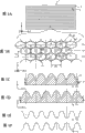
Be easy to viewpoint from moulding, the cone shape that tectosome 3 preferably has cone shape or makes cone shape extend or shrink to trajectory direction.The cone shape that tectosome 3 preferably has axisymmetric cone shape or makes cone shape extend or shrink to trajectory direction.If engage with the tectosome 3 of adjacency, tectosome 3 except with bottom that the tectosome 3 of adjacency engages the cone shape that preferably has axisymmetric cone shape or make cone shape extend or shrink to trajectory direction.Cone shape for example is cone shape, truncated cone shape, elliptic cone shape, oval frustum shape, polygonal cone-shaped (for example pyrometric cone shape, quadrangle cone shape, pentagonal pyramid shape etc.), polygonal frustum shape etc.As mentioned above, the notion of the cone shape here also comprises elliptic cone shape, oval frustum shape and polygonal frustum shape except cone shape, truncated cone shape and polygonal cone-shaped.And truncated cone shape is meant the shape at the top of having cut away cone shape, and oval frustum shape is meant the shape at the top of having cut away elliptic cone.Polygonal frustum shape is meant the shape at the top of having cut away polygonal awl.And the shape of tectosome 3 is not limited to above-mentioned shape, can adopt shapes such as aciculiform, cylindrical, cheese, tent like.The tent like here is to instigate the conical surface of polygonal awl or polygonal frustum to cave in into the shape of concavity.
As Fig. 2 and shown in Figure 4, tectosome 3 preferred bottom surfaces are ellipse, Long Circle or the avette cone structures with major axis and minor axis, and the top is the elliptic cone shape of curved surface.Or as shown in Figure 5, preferred bottom surface is ellipse, Long Circle or the avette cone structure with major axis and minor axis, and the top is smooth oval frustum shape.In case form such shape, can improve the filling rate of column direction.
From improving the viewpoint of reflection characteristic, preferably the degree of tilt at top little, become big cone shape (with reference to figure 4) gradually from pars intermedia towards the bottom angled degree.And from improving reflection characteristic and seeing through the viewpoint of characteristic, the degree of tilt that is preferably formed pars intermedia is smooth cone shape (with reference to figure 5) than big conical in shape (with reference to figure 2) or the top in bottom and top.If tectosome 3 has elliptic cone shape or oval frustum shape, then the long axis direction of preferred its bottom surface is parallel with the bearing of trend of track.In Fig. 2 etc., each tectosome 3 is of similar shape respectively, but the shape of tectosome 3 is not limited to this, also can form the tectosome 3 of two or more shapes at matrix surface.And tectosome 3 also can form one with matrix 2.
To shown in Figure 6, preferably on every side part or all of tectosome 3, teat 4 is set as Fig. 2, Fig. 4.By like this,, also can reduce reflectivity even the filling rate of tectosome 3 is low.Specifically be as Fig. 2, Fig. 4 and shown in Figure 5, teat 4 for example is set between adjacent tectosome 3.And, as shown in Figure 6, also elongated teat 4 can be arranged on around the tectosome 3 all or part of.This elongated teat 4 for example from the top of tectosome 3 towards lower extended.The shape of teat 4 can be section triangle and cross section quadrangle etc., but is not limited to these shapes, can select according to the complexity that is shaped.And, also can make part or all roughening around the tectosome 3, form trickle concavo-convex.Specifically be the surperficial roughening that for example can make between the adjacent tectosome 3, form trickle concavo-convex.And, also can for example form small hole in the top on the surface of tectosome 3.
The height H 1 preferred height H 2 of the tectosome 3 on the bearing of trend of track less than the tectosome on the column direction 3.Be the height H 1 of tectosome 3, the relation that H2 preferably satisfies H1<H2.This be because if for the relation that satisfies H1 〉=H2 array structure body 3, the configuration section of bearing of trend that then needs to increase track is apart from P1, so the filling rate of the tectosome on the bearing of trend of track 3 reduces.If filling rate reduces, will cause reflection characteristic to reduce.
In addition, the depth-width ratio of tectosome 3 is not limited to all identical situations, also can make each tectosome 3 have certain height distribute (for example depth-width ratio is in 0.83~1.46 scope).By the tectosome 3 that setting has height profile, can reduce the wavelength dependency of reflection characteristic.Therefore can realize having the optical element of good preventing reflection characteristic.
The height profile here is meant that the tectosome 3 with two or more height (degree of depth) is arranged on the surface of matrix 2.That is, be meant to have as the tectosome 3 of the height of benchmark and have the surface that is arranged on matrix 2 with the tectosome 3 of this tectosome 3 differing heights.Have with the tectosome 3 of benchmark differing heights for example periodically or aperiodicity ground (at random) be arranged on the surface of matrix 2.As its periodic direction bearing of trend that for example is track, column direction etc.
Preferably the periphery at tectosome 3 is provided with the skirt shape 3a of portion.This is in order can easily optical element and mould etc. to be peeled off in the manufacturing step of optical element.The skirt shape 3a of portion here is meant the teat of the periphery of the bottom that is arranged on tectosome 3.From the angle of above-mentioned peel property, this skirt shape 3a of portion preferably has the curved surface of highly mild reduction towards the direction of bottom from the top of tectosome 3.In addition, the skirt shape 3a of portion can only be arranged on the part of periphery of tectosome 3, but in order to improve above-mentioned stripping performance, preferably is arranged on the whole periphery of tectosome 3.And tectosome 3 is under the situation of recess, and skirt shape portion becomes and is arranged on the curved surface that tectosome 3 is the open circumferential of recess.
Height (degree of depth) to tectosome 3 is not particularly limited, and can suitably set according to the light wavelength scope that sees through, and for example is set in the scope about 236nm~450nm.The depth-width ratio of tectosome 3 (highly/configuration section apart from) is more than or equal to 0.6 smaller or equal to 1.5, is preferably greater than to equal 0.81 smaller or equal to 1.46, further is preferably greater than to equal 0.94 smaller or equal to 1.28 scope.If less than 0.6, then have the trend that reflection characteristic and through performance reduce, if surpass 1.5, the stripping performance that then has a tectosome 3 when making optical element reduces and the trend of reproduction replica gallantly.And from the viewpoint of further raising reflection characteristic, the depth-width ratio of tectosome 3 preferably sets the scope 0.94~1.46.In order further to improve through performance, the depth-width ratio of tectosome 3 preferably sets the scope 0.81~1.28.
And the depth-width ratio of tectosome 3 (highly/configuration section apart from) is preferably more than or equal to 0.6 smaller or equal to 5, further is preferably greater than to equal 0.6 smaller or equal to 4 scope.If less than 0.6, then has the trend that reflection characteristic and through performance reduce, when surpassing 5, if then improve the processing of release property, for example on former dish, implement fluorine coating etc. or add as the transfer printing resin that the silicon class is added material or the fluorine class is added material etc., also have the trend of transfer printing reduction.And if depth-width ratio surpasses 4, then luminous reflectance does not have big variation, therefore in order to improve the luminous reflectance and the demoulding easily, preferably makes depth-width ratio smaller or equal to 4.
The elastic modulus of material that forms tectosome 3 more than or equal to 1MPa smaller or equal to 1200MPa.If less than 1MPa, then the tectosome of adjacency is attached to each other in transfer step, and the shape of tectosome 3 becomes the shape different with required form, can not obtain needed reflection characteristic.If surpass 1200MPa, then when wiping, be not easy contact between the tectosome of adjacency, can not extrude the spot of infiltrating between the tectosome etc.
In addition, in the present invention, by following formula (1) definition depth-width ratio.
Depth-width ratio=H/P ... (1)
Wherein, H: the height of tectosome, P: average configuration section is apart from (average period)
Here define average configuration section apart from P by following formula (2).
Average configuration section is apart from P=(P1+P2+P2)/3 ... (2)
Wherein, P1: the configuration section of the bearing of trend of track is apart from (track bearing of trend cycle), P2: with respect to track bearing of trend ± the θ direction (wherein, θ=60 °-δ, wherein, δ is preferably 0 °<δ≤11 °, further preferred 3 °≤δ≤6 °) configuration section apart from (θ direction cycle)
And, with the height of the column direction of tectosome 3 height H as tectosome 3.The height of the track extending direction (directions X) of tectosome 3 is less than the height of column direction (Y direction), and the height of the part beyond the track extending direction of tectosome 3 and the height of column direction are much at one, therefore represent the height of sub-wavelength tectosome with the height of column direction.Wherein, tectosome 3 is under the situation of recess, and the height H of the tectosome in the above-mentioned formula (1) becomes the depth H of tectosome.
The configuration section of supposing the tectosome 3 in the same track is apart from being P1, and when the configuration section distance of the tectosome 3 between two tracks of adjacency was P2, ratio P1/P2 preferably satisfied the relation of 1.00≤P1/P2≤1.1 or 1.00<P1/P2≤1.1.By in this numerical range, can improve the filling rate of tectosome with elliptic cone or oval frustum shape, therefore can improve preventing reflection characteristic.
The filling rate of the tectosome 3 of matrix surface is the upper limit and more than or equal to 65% with 100%, is preferably greater than to equal 73%, further in preferred 86% the scope.By filling rate being formed on this scope, can improve preventing reflection characteristic.In order to improve filling rate, preferably the bottom of the tectosome 3 of adjacency is engaged with each other or the ellipticity etc. of adjusting the tectosome bottom surface makes tectosome 3 distortion.
At this, the filling rate of tectosome 3 (average filling rate) is the following value of obtaining.
At first, use sweep electron microscope (SEM:Scanning Electron Microscope) to take the surface of optical element 1 with Top View.Extract unit lattice Uc then from captured SEM photo arbitrarily out, the configuration section of measuring this unit lattice Uc is apart from P1 and track pitch Tp (with reference to Figure 1B).And, be positioned at the base area S of the tectosome 3 in the middle of this unit lattice Uc by the Flame Image Process measurement.Then, utilize the configuration section of measuring to obtain filling rate by following formula (3) apart from P1, track pitch Tp and base area S.
Filling rate=(S (hex.)/S (unit)) * 100 ... (3)
Unit lattice area: S (unit)=P2 * 2Tp
The base area that is present in the tectosome in the unit lattice: S (hex.)=2S
Ten the unit lattice of extracting out arbitrarily from the SEM photo of taking is carried out above-mentioned filling rate computing.Simply measured value is averaged the average rate that (arithmetical mean) obtains filling rate then, with its filling rate as the tectosome 3 of matrix surface.
Filling rate when having pair tectosome such as teat 4 when tectosome 3 is overlapping or between the tectosome 3 can be obtained by the following method, is about to the part corresponding with 5% of the height of tectosome 3 and judges the area ratio as threshold value.
Fig. 7 is the key diagram of the boundary of tectosome 3 computing method of filling rate when not knowing.When the boundary of tectosome 3 is not known, observe by section SEM, as shown in Figure 7, the part of 5% (=(d/h) * 100) that will be equivalent to tectosome 3 height h is as threshold value, and the diameter that converses tectosome 3 with this height d is obtained filling rate.The bottom surface of tectosome 3 is under the situation of ellipse, utilizes major axis and minor axis to carry out same processing.
Fig. 8 is the figure of the bottom shape the when ellipticity of the bottom surface of tectosome 3 is changed.Ellipticity oval shown in Fig. 8 A to Fig. 8 D is respectively 100%, 110%, 120% and 141%.By such change ellipticity, the filling rate of the tectosome 3 of matrix surface is changed.If tectosome 3 forms accurate hexagonal pattern, then the ellipticity e of tectosome bottom surface is preferably 100%<e<150%.By being formed on this scope, can improve the filling rate of tectosome 3, obtain good preventing reflection characteristic.
Here, suppose that the diameter of the trajectory direction (directions X) of tectosome bottom surface is a, when being b, utilize (a/b) * 100 definition ellipticity e with the diameter of the column direction (Y direction) of its quadrature.In addition, diameter a, the b of tectosome 3 are values of obtaining as described below.Use sweep electron microscope (SEM:Scanning Electron Microscope) with the surface that TopView takes optical element 1, from captured SEM photo, extract ten tectosomes 3 arbitrarily out.Measure each bottom surface diameter a, b of the tectosome of being extracted out 3 then.Simply measured value a, b are averaged (arithmetical mean), obtain the mean value of diameter a, b, as diameter a, the b of tectosome 3.
Fig. 9 A is the configuration illustration with tectosome 3 of taper shape or truncated cone.Fig. 9 B is the configuration illustration with tectosome 3 of oval taper or oval taper type.Shown in Fig. 9 A and Fig. 9 B, the mode that tectosome 3 preferably overlaps each other with its underpart engages.Particularly, the bottom of tectosome 3 preferably with part or all the lower bond that is in tectosome 3 in the syntople.More specifically, preferably trajectory direction, the θ direction or on both direction the bottom of tectosome 3 be engaged with each other.Fig. 9 A, 9B show the example of all lower bond of the tectosome 3 that is in the syntople.By such junction structure 3, can improve the filling rate of tectosome 3.Preferably tectosome is bonded with each other according to the peaked part below 1/4 of the wave band of the light of the optical path length of having considered refractive index under environment for use.Like this, obtain good preventing reflection characteristic.
Shown in Fig. 9 B, under the situation about being engaged with each other in tectosome 3 bottoms with oval taper or oval taper type, the height at junction surface for example shoals according to the order of junction surface a, b, c.
[structure of roller mother matrix]
Figure 10 is the topology example that is used to make the roller mother matrix of the optical element with said structure.As shown in figure 10, roller mother matrix 11 for example has following structure, that is, with the pitch with light wavelength equal extent such as visible lights a plurality of recesses being set on the surface of former dish 12 is tectosome 13.Former dish 12 has cylindrical or columnar shape.The material of disk 12 for example can use glass, but is not limited to this material.Utilize the former dish exposure device of roller described later, ground, space connects two-dimensional pattern, makes the Rotation Controllers of reversal of poles formatter signal and pen recorder produce signal synchronously at each track, with CAV, with suitable feed pitch composition.By writing down hexagonal pattern or accurate hexagonal pattern like this.The frequency by suitably setting the reversal of poles format signal and the revolution of roller can form the unified grid pattern of spatial frequency at required posting field.
[manufacture method of optical element]
Describe with regard to the manufacture method of the optical element 1 of said structure below with reference to Figure 11 to Figure 13.
The manufacture method of the optical element of first embodiment is included on the former dish resist film forming step that forms resist layer, utilize the former dish exposure device of roller on resist film, form the moth eye pattern sub-image step of exposure and will form the development step that the resist layer of sub-image develops.But also comprise the etching step that utilizes plasma etching to make the roller mother matrix, make the copy step of replicated substrate by ultraviolet hardening resin.
(structure of exposure device)
At first, with reference to Figure 11 the structure of the former dish exposure device of roller shape of the step of exposure that is used for the moth eye pattern is described.The former dish exposure device of this roller shape constitutes based on optical disc recording apparatus.
In modulation optical system 25, by collector lens 26 laser 15 is concentrated on and comprises quartz (SiO
2) acousto-optic element (AOM:acousto-optic modulator) 27 that waits.Laser 15 is become parallel beam by acousto-optic element 27 intensity modulated and after dispersing by lens 28.The laser 15 that penetrates from modulation optical system 25 device 31 reflections that are reflected, thereby level and be directed to mobile optical platform (table) 32 abreast.
Mobile optical platform 32 comprises optical beam expander 33 and object lens 34.After the laser 15 of guiding mobile optical platform 32 was shaped as the beam shape of hope by optical beam expander 33, by object lens 34, the resist layer on former dish 12 shone.Former dish 12 is placed on the turntable (turn table) 36 that is connected with spindle drive motor 35.In addition, make 12 rotations of former dish, simultaneously, laser 15 is moved along the short transverse of former dish 12, and to resist layer irradiating laser 15 intermittently, thereby carry out the step of exposure of resist layer.The sub-image that forms is for having the substantially elliptical of major axis at circumferencial direction.Move mobile laser 15 by mobile optical platform 32 to arrow R direction.
Exposure device comprises the control gear 37 that is used for resist layer is formed sub-image, and wherein, this sub-image is corresponding to the two-dimensional pattern of hexagonal grid shown in Figure 1B or accurate hexagonal grid.Control gear 37 comprises formatter (formatter) 29 and driver 30.Formatter 29 comprises reversal of poles portion, and this reversal of poles portion is used to control the timing (timing) to resist layer irradiating laser 15.Driver 30 is used for the output and the guide sound optical element 27 of receiving polarity counter-rotating portion.
In the former dish exposure device of this roller shape, corresponding each track makes the Rotation Controllers of reversal of poles formatter signal and pen recorder synchronously produce signal, so that ground, two-dimensional pattern space connects, and carries out intensity modulated by acousto-optic element 27.By in the constant mode of angular velocity (CAV) with suitable rotation number and suitable modulating frequency and suitable conveying section apart from forming pattern, can write down hexagonal pattern or accurate hexagonal pattern.For example, shown in Figure 10 B,, will be made as 300nm with respect to the cycle of the about 60 ° of directions of circumferencial direction (-60 ° of directions approximately), as long as the conveying section distance is made as 251nm (Pythagorean theorem) for the cycle with circumferencial direction is made as 315nm.Change the frequency of reversal of poles formatter signal by the revolution (for example 1800rpm, 900rpm, 450rpm, 225rpm) of roller.For example, the frequency with the corresponding respectively reversal of poles formatter signal of revolution 1800rpm, 900rpm, 450rpm, the 225rpm of roller is 37.70MHz, 18.85MHz, 9.34MHz, 4.71MHz.Obtain by following method at the consistent accurate hexagonal pattern of space frequency on the posting field of hope (circumference 315nm cycle, about 60 degree directions (-60 ° of directions approximately) 300nm cycle of circumferencial direction): the optical path that far-ultraviolet laser is enlarged into 5 times by (BEX) 33 of the optical beam expander on the mobile optical platform 32, object lens 34 by opening number (NA) 0.9 shine resist layer on former dish 12 with it then, form fine sub-image.
(resist film forming step)
At first, shown in Figure 12 A, prepare a columniform former dish 12.This former dish 12 is such as being the former dish of glass.Then, shown in Figure 12 B, form resist layer 14 on the surface of former dish 12.The material of resist layer 14 is such as adopting in organic class resist and the mineral-type resist any.Organic class resist is such as adopting phenolics class resist or chemical reinforcing type resist.
(step of exposure)
Then, shown in Figure 12 C, make former dish 12 rotations, simultaneously laser (exposing light beam) 15 is shone in resist layer 14 with the former dish exposure device of above-mentioned roller shape.At this moment, move to the short transverse of former dish 12 (with the direction of the central axes of cylindrical or columnar former dish 12) by making laser 15, irradiating laser intermittently simultaneously, thus make whole resist layer 14 exposures.Thus, on whole of resist layer 14 to form the corresponding sub-image 16 of track with laser 15 with the pitch of wavelengths of visible light equal extent.
Sub-image 16 constitutes the multiple row track such as being configured in former panel surface, and forms hexagonal pattern or accurate hexagonal pattern.Sub-image 16 is such as being the elliptical shape that has long axis direction at the track bearing of trend.
(development step)
Then, rotate former dish 12, simultaneously developer solution is dropped on the resist layer 14, as shown in FIG. 13A, resist layer 14 is carried out development treatment.As shown in the figure, when resist layer 14 by eurymeric (positive) when resist forms, compare with non-exposure portion through the exposure portion of laser 15 exposures, with respect to the dissolution velocity increase of developer solution, therefore, be formed on the resist layer 14 with sub-image (exposure portion) 16 corresponding patterns.
(etching step)
Next, the pattern (corrosion-resisting pattern) that is formed on the resist layer 14 on the former dish 12 as mask (mask), is carried out etch processes to the surface of former dish 12.Thereby, shown in Figure 13 B, can obtain the track bearing of trend have the elliptic cone shape of long axis direction or oval frustum shape recess, be tectosome 13.Engraving method is such as being undertaken by dry-etching.At this moment, handle, thereby can form pattern such as pyramidal tectosome 13 by carrying out etch processes and polishing (ashing) alternately.The former dish of glass (master) of the degree of depth more than three times (select than be more than 3) of resist layer 14 can be made simultaneously, and the high depth-width ratio of tectosome 3 can be realized.
According to above-mentioned processing, can obtain having depth ratio as being the hexagonal pattern of the spill to the 350nm or the former dish 11 of roller shape of accurate hexagonal pattern about 120nm.
(copy step)
Then, such as the former dish 11 of roller shape is close to the sheet matrixes 2 such as (sheet) that is coated with transfer materials, and when making its sclerosis, peels off irradiation ultraviolet radiation.By like this shown in Figure 13 C, protuberance is that a plurality of tectosomes are formed on first first type surface of matrix 2, makes the optical element 1 of the UV cured duplicated film of moth eye etc.
Transfer materials as required, can comprise filling agent or functional additive etc. such as being made of UV cured material and initiating agent (initiator).
UV cured material is specially the material that is mixed with single or multiple following materials such as being made of simple function group monomer, bifunctional monomer, polyfunctional monomer etc.
As the simple function group monomer, for example can enumerate: carboxylic acids (acrylic acid), hydroxy kind (2-Hydroxy ethyl acrylate, acrylic acid-2-hydroxy propyl ester, acrylic acid-4-hydroxyl butyl ester), alkyls, alicyclic ring class (isobutyl acrylate, tert-butyl acrylate, Isooctyl acrylate monomer, dodecyl acrylate, octadecyl acrylate, isobornyl acrylate (isobonyl acrylate), the acrylic acid cyclohexyl ester), other functional monomer (2-methoxy ethyl acrylate, methoxyl EDIA (methoxyethylene glycol acrylate), 2-ethoxyethyl group acrylate, the acrylic acid tetrahydro furfuryl ester, benzyl acrylate, second carbitol acrylate, phenoxyethyl acrylate, acrylic acid dimethylamino ethyl ester, the dimethylamino-propyl acrylamide, N, the N-DMAA, acryloyl morpholine, the n-N-isopropylacrylamide, N, N-diethyl acrylamide, the N-vinyl pyrrolidone, 2-(perfluoro capryl) ethyl propylene acid esters, 3-perfluoro hexyl-2-hydroxypropyl acrylate, 3-perfluoro capryl-2-hydroxypropyl acrylate, 2-perfluor decyl ethyl acrylate, 2-(perfluor-3-methyl butyl) ethyl propylene acid esters, 2,4,6-tribromphenol acrylate, 2,4,6-tribromphenol methacrylate, 2-(2,4, the 6-tribromophenoxy) the ethyl propylene acid esters), with acrylic acid-2-ethyl caproite etc.
As the bifunctional monomer, for example can enumerate: tri (propylene glycol) diacrylate, trimethylolpropane allyl ether, urethane acrylate etc.
As polyfunctional monomer, for example can enumerate: trimethylolpropane triacrylate, double pentaerythritol C5 methacrylate, double pentaerythritol methacrylate and double trimethylolpropane tetraacrylate etc.
As initiating agent, for example can enumerate: 2,2-dimethoxy-1,2-diphenyl second-1-ketone, 1-hydroxy-cyclohexyl phenyl ketone, 2-hydroxy-2-methyl-1-phenyl third-1-ketone etc.
As filling agent such as adopting in inorganic particles and the organic fine particles any.For example can enumerate SiO as inorganic particles
2, TiO
2, ZrO
2, SnO
2, Al
2O
3Deng metal oxide microparticle.
As functional additive, for example can enumerate: levelling agent, surface conditioner, defoamer etc.Material as matrix 2, for example can enumerate methyl methacrylate (being total to) polymkeric substance, polycarbonate, styrene (being total to) polymkeric substance, copolymer of methyl methacrylatestyrene, cellulose diacetate, Triafol T, acetylbutyrylcellulose, polyester, polyamide, polyimide, polyethersulfone, polysulfones, polypropylene, polymethylpentene, Polyvinylchloride, polyvinyl acetal, polyetherketone, polyurethane and glass etc.
The manufacturing process of matrix 2 does not have specific qualification, can be the injection molding body, can be to be extruded into body yet, can also be to be cast as body.As required, also can carry out surface treatments such as corona (corona) processing to matrix surface.
<2. second embodiment 〉
[structure of optical element]
Figure 15 A is the summary vertical view that a structure example of the related optical element of second embodiment of the present invention is shown.Figure 15 B is the vertical view that amplifies the part that the optical element shown in Figure 15 A is shown.Figure 15 C is track T1, the T3 among Figure 15 B ... sectional view.Figure 15 D is track T2, the T4 among Figure 15 B ... sectional view.Figure 15 E be illustrate be used to form with Figure 15 B in track T1, T3 ... the summary line chart of the modulation waveform of the laser of corresponding sub-image.Figure 15 F be illustrate be used to form with Figure 15 B in track T2, T4 ... the summary line chart of the modulation waveform of the laser of corresponding sub-image.
The difference of the optical element 1 that second embodiment is related and the optical element of first embodiment is: each tectosome 3 constitutes quadrilateral grid pattern or accurate quadrilateral grid pattern between three row tracks of adjacency.In the present invention, so-called accurate quadrilateral grid pattern is different from the square grid pattern, and it is meant the quadrilateral grid pattern that bearing of trend (directions X) along track is stretched and has distorted.
The height of tectosome 3 or the degree of depth are not special to be limited, for example can 159nm~312nm degree (about).With respect to the pitch P2 on 45 ° of directions of track (pact) for example is about 275nm~297nm.The depth-width ratio of tectosome 3 (highly/and the configuration section distance) for example be about 0.54~1.13.In addition, the depth-width ratio that is not limited in each tectosome 3 is whole identical situations, also can constitute each tectosome 3 and have the certain height distribution.
The configuration section of the tectosome 3 in the preferred same trajectories apart from P1 greater than the configuration section of the tectosome 3 between two tracks of adjacency apart from P2.In addition, when with the configuration section of the tectosome in the same trajectories 3 apart from being set at P1, and with the configuration section of the tectosome 3 between two tracks of adjacency when being set at P2, preferred P1/P2 satisfies the relation of 1.4<P1/P2≤1.5.By being set at such numerical range, thereby the filling rate of tectosome 3 can be improved, therefore preventing reflection characteristic can be improved with elliptic cone shape or oval frustum shape.In addition, preferably with respect to the height of the tectosome 3 on 45 ° of directions of track or the about 45 ° of directions or the degree of depth the height or the degree of depth less than the tectosome on the track bearing of trend 3.
Preferably the height H 2 in the orientation (θ direction) of the tectosome 3 that tilts with respect to the track bearing of trend is less than the height H 1 of the tectosome on the track bearing of trend 3.That is, preferably satisfy the height H 1 of tectosome 3 and the relation that H2 satisfies H1>H2.
Figure 16 is the synoptic diagram of the bottom shape when changing the ellipticity of bottom surface of tectosome 3. Ellipticity 3
1, 3
2, 3
3Be respectively 100%, 163.3% and 141%.By change ellipticity like this, thereby can change the filling rate of the tectosome 3 of matrix surface.When tectosome 3 formed quadrilateral grid or accurate quadrilateral grid pattern, the ellipticity e of preferable configuration body bottom surface was 150%≤e≤180%.This be because: by ellipticity e is set in this scope, thereby can improve the filling rate of tectosome 3, obtain remarkable preventing reflection characteristic.
The filling rate of the tectosome 3 of matrix surface is the upper limit with 100%, and is more than or equal to 65%, is preferably more than to equal 73%, more preferably more than or equal in 86% the scope.By filling rate is set in such scope, thereby can improve preventing reflection characteristic.
Here, the filling rate of tectosome 3 (average filling rate) is the following value of obtaining.
At first, take the surface of optical element 1 with top view (Top View) with scanning electron microscope (SEM:Scanning Electron Microscope).Then, select unit lattice Uc at random from captured SEM photo, the configuration section of measuring this unit lattice Uc is apart from P 1 and track pitch Tp (with reference to figure 15B).Then, measure by the base area S of Flame Image Process any one tectosome 3 in four tectosomes 3 that comprised among this unit lattice Uc.Subsequently, use the configuration section of being measured to obtain filling rate according to following formula (4) apart from P1, track pitch Tp and base area S.
Filling rate=(S (tetra)/S (unit)) * 100 ... (2)
Unit lattice area: S (unit)=2 * ((P1 * Tp) * (1/2))=P1 * Tp
The base area that is present in the tectosome in the unit lattice: S (tetra)=S
10 unit lattice of selecting at random from captured SEM photo are carried out above-mentioned filling rate computing.Then, average simply (arithmetic mean) measured value is obtained the average rate of filling rate, and with its filling rate as the tectosome 3 of matrix surface.
Figure 17 shows a structure example of the former dish of roller shape that is used to make the optical element with said structure.The difference of the former dish of roller shape in the former dish of this roller shape and first embodiment is: in its surface, the tectosome 13 of concavity has constituted quadrilateral grid pattern or accurate quadrilateral grid pattern.
[structure of roller mother matrix]
Utilize the former dish exposure device of roller, ground, space connects two-dimensional pattern, makes the Rotation Controllers of reversal of poles formatter signal and pen recorder produce signal synchronously at each track, with CAV, with suitable feed pitch composition.By writing down quadrilateral grid pattern or accurate quadrilateral grid pattern like this.The preferably frequency by suitably setting reversal of poles formatter signal and the revolution of roller will be on the irradiation of the unified grid pattern of required posting field spatial frequency by laser be formed on resist on the former dish 12.
<3. the 3rd embodiment 〉
[structure of optical element]
Figure 18 A is the schematic plan view of topology example of the optical element of the 3rd embodiment of the present invention.Figure 18 B is the amplification view of the part of the optical element shown in Figure 18 A.Figure 18 C be Figure 18 B track T1, T3 ... on cut-open view.Figure 18 D be Figure 18 B track T2, T4 ... on cut-open view.
The optical element 1 of the 3rd embodiment and the difference of first embodiment are that track T has circular shape, and tectosome 3 is configured to circular arc.Shown in Figure 18 B, (arrangement body 3 forms the accurate hexagonal pattern on the each point that is centered close to a1~a7 of tectosomes 3 between the T1~T3) at three row tracks of adjacency.At this, it is different with the regular hexagon grid pattern that accurate hexagonal pattern is meant, the hexagonal pattern after being out of shape along the circular arc of track T.Or different with the regular hexagon grid, along the distortion of the circular arc of track T and by the bearing of trend (directions X) to track stretch, hexagonal pattern after the distortion.The structure of optical element 1 in addition is identical with first embodiment, omits explanation.
[structure of optical disc master]
Figure 19 A, Figure 19 B are the topology examples that is used to make the optical disc master of the optical element with said structure.Shown in Figure 19 A, Figure 19 B, it is the structure of tectosome 43 that optical disc master 41 has at the discoidal former dish 42 surface a plurality of recesses of arrangement.This tectosome 43 be with optical element 1 below the wavestrip of the light under the environment for use, for example with the pitch of wavelength of visible light same degree two-dimensional arrangements periodically.Tectosome 43 for example is configured on circular concentric or the spiral helicine track.
In addition the structure of optical disc master 41 is identical with the roller mother matrix 11 of first embodiment, omits explanation.
[manufacture method of optical element]
At first the exposure device that just is used to make the optical disc master 41 with said structure with reference to Figure 20 describes.
Mobile optical platform 32 comprises optical beam expander 33, catoptron 38 and object lens 34.After the laser 15 of guiding mobile optical platform 32 is shaped to needed beam shape by optical beam expander 33, the resist layer irradiation on discoidal former dish 42 by catoptron 38 and object lens 34.Former dish 42 be placed on spindle motor (spindle motor) 35 turntables that are connected (omit diagram) on.Make former dish 42 rotations then, one side makes laser 15 move the one side resist layer irradiating laser on former dish 42 off and on to the radius of turn direction of former dish 42 simultaneously, by carrying out the step of exposure of resist layer like this.The sub-image that forms becomes the summary ellipse that has major axis at circumferencial direction.Laser 15 mobile by to the arrow R of mobile optical platform 32 direction.
Exposure device shown in Figure 20 comprises control gear 37, and control gear 37 forms the sub-image that constitutes with the hexagonal grid shown in Figure 18 B or the two-dimensional pattern of accurate hexagonal grid on resist layer.Control gear 37 comprises formatter 29 and driver 30.Formatter 29 has reversal of poles portion, and this reversal of poles portion control laser 15 is to the irradiation time of resist layer.Driver 30 is accepted the output of reversal of poles portion, guide sound optical element 27.
And, change the control signal of reversal of poles portion gradually, make spatial frequency (pattern density of sub-image, P1:330nm, P2:300nm or P1:315nm, P2:275nm or P1:300nm, P2:265nm) unified.More particularly, one side makes to 15 cycles of laser of resist layer irradiation at each track and changes the one side exposure, and control gear 37 carries out the frequency modulation (PFM) of laser 15, makes P1 be about 330nm (or 315nm, 300nm) on each track T.That is,, modulate control in the mode that the exposure period of laser shortens along with track position is left discoidal former dish 42 centers.By can on whole base plate, forming the unified nano-pattern of spatial frequency like this.
Below describe with regard to an example of the manufacture method of the optical element of the 3rd embodiment of the present invention.At first utilize exposure device,, make optical disc master 41 in the same manner with above-mentioned first embodiment except to being formed on resist layer on the discoidal former dish exposes with said structure.Make this optical disc master 41 and matrix 2 driving fits such as acrylic acid (ester) sheet that applied ultraviolet hardening resin then, irradiation ultraviolet radiation, make the ultraviolet hardening resin sclerosis after, matrix 2 is peeled off from optical disc master 41.By obtaining having arranged the discoidal optical element 1 of a plurality of tectosomes 3 like this on the surface.Downcut the optical element 1 of rectangle isotactic setting shape then from this discoidal optical element 1.By the required optical element 1 of such manufacturing.
According to the 3rd embodiment, can similarly obtain the production efficiency height when tectosome 3 is arranged in a straight line shape, have the optical element 1 of good preventing reflection characteristic.
<4. the 4th embodiment 〉
Figure 21 A is the schematic plan view of topology example of the optical element of the 4th embodiment of the present invention, and Figure 21 B is the amplification view of the part of the optical element shown in Figure 21 A.
The optical element 1 of the 4th embodiment and the difference of first embodiment are tectosome 3 is arranged on the track (hereinafter referred to as swinging track) that crawls.The swing of each track on the matrix 2 is preferably carried out synchronously.I.e. swing is swing synchronously preferably.By making swing synchronous like this, can keep the unit lattice shape of hexagonal grid or accurate hexagonal grid, keep high fill-ratio.The waveform of swinging track for example can be sine wave, triangular wave etc.The waveform of swinging track is not limited to periodic waveform, also can be acyclic waveform.The wobble amplitude of swinging track for example can be chosen in ± 10 μ m about.In the 4th embodiment, except above-mentioned, identical with first embodiment.
According to the 4th embodiment,, can suppress the inhomogeneous of outward appearance because tectosome is arranged on the swinging track.
<5. the 5th embodiment 〉
Figure 22 A is the schematic plan view of topology example of the optical element of the 5th embodiment of the present invention.Figure 22 B is the amplification view of the part of the optical element shown in Figure 22 A.Figure 22 C be Figure 22 B track T1, T3 ... on cut-open view.Figure 22 D be Figure 22 B track T2, T4 ... on cut-open view.Figure 23 is the part amplification stereogram of the optical element shown in Figure 22 A.
The optical element 1 of the 5th embodiment and the difference of first embodiment are that a plurality of recesses are that tectosome 3 is arranged in matrix surface.The shape of this tectosome 3 is to turn the convex of the tectosome 3 of first embodiment around the formation spill.As described above tectosome 3 is formed under the situation of recess, carry out to give a definition, promptly recess is that the peristome (intake section of recess) of tectosome 3 is the bottom, and the foot of matrix 2 depth directions (deepest part of recess) is the top.That is be tectosome 3 definition top and bottoms, by non-entity space.And in the 5th embodiment, because tectosome 3 is recesses, so the height H of the tectosome 3 in the formula (1) etc. becomes the depth H of tectosome 3.
In the 5th embodiment, all identical except above-mentioned with first embodiment.In the 5th embodiment, turn the shape of the convex configuration body 3 of first embodiment around the formation spill, therefore can obtain the effect identical with first embodiment.
<6. the 6th embodiment 〉
The elasticity of the material of formation tectosome 3 is low more, and the sliding during wiping is poor more, and wiping is low more.Therefore, in the 6th embodiment, contain at least a compound of from fluoride compound and silicon compounds, selecting, improve sliding, improve wiping by making the tectosome surface.
Can the not influence of wiping fingerprint although these materials are contained on the tectosome surface to whether, can suppress to have adhered to behind the fingerprint fingerprint and infiltrate and spread.Therefore, by elastic modulus and depth-width ratio are remained on certain scope, and improve the contact angle of oleic acid, can form the high antireflection structure of soil resistance 3.
As the method that makes the tectosome surface contain fluoride compound or silicon compounds following method is for example arranged, that is, after adding the method for fluoride compound after-hardening and forming tectosome, the resin material that forms tectosome forms the method etc. of the surface-treated layer that contains fluoride compound on the tectosome surface.
Figure 24 is the cut-open view of topology example of the optical element of the 6th embodiment of the present invention.As shown in figure 24, the optical element 1 of the 6th embodiment and the difference of first embodiment are also have surface-treated layer 5 on the male and fomale(M﹠F) that has formed tectosome 3.
The oleic acid contact angle that has formed the surface of surface-treated layer 5 is preferably greater than and equals 30 degree, further is preferably greater than to equal 90 degree.If more than or equal to 90, then can suppress to spread attached to spots such as the fingerprint infiltration of optical element surface.Surface-treated layer 5 for example contains fluorochemicals or silicon compounds.
[silicon compounds]
The silicon compounds for example is a silicone oil, silicon surface active agent etc.Silicone oil can roughly be divided into straight silicone oil (straight silicone oil) and modified silicon oil according to the kind of the organic group that combines with silicon atom.
Straight silicone oil is that methyl, phenyl, hydrogen atom are combined with silicon atom as substituting group.Straight silicone oil for example is dimethyl silicon oil, methyl phenyl silicone oil etc.
Modified silicon oil for example is the silicone oil behind the introducing organic substituent in the straight silicone oil of dimethyl-silicon wet goods.Modified silicon oil is divided into two kinds of nonactive silicone oil and active silicone oil.
Nonactive silicone oil for example is alkyl/aralkyl modified silicon oil, polyether modified silicon oil, higher fatty acid modified silicon oil, amino-modified silicone oil, epoxide modified silicone oil, carboxy-modified silicone oil, pure modified silicon oil etc.
Active silicone oil for example is amino-modified silicone oil, epoxide modified silicone oil, carboxy-modified silicone oil, pure modified silicon oil etc.
Silicone oil specifically is the L-45 of Japanese You Nika joint-stock company, L-9300, FZ-3704, FZ-3703, FZ-3720, FZ-3786, FZ-3501, FZ-3504, FZ-3508, FZ-3705, FZ-3707, FZ-3710, FZ-3750, FZ-3760, FZ-3785, Y-7499, the KF96L of chemical company of SHIN-ETSU HANTOTAI, KF96, KF96H, KF99, KF54, KF965, KF968, KF56, KF995, KF351, KF352, KF353, KF354, KF355, KF615, KF618, KF945, KF6004, FL100 etc.
Silicon surface active agent for example is that the part with methyl-silicone oil is replaced as hydrophilic radical.The displacement position of hydrophilic radical is the side chain, two ends of silicone oil, single end, two terminal side chains etc.Hydrophilic radical is polyethers, polyglycereol, pyrrolidone, betaine, sulfate, phosphate, quaternary salt etc.
Wherein, preferred hydrophobic grouping is a dimethyl polysiloxane, and hydrophilic radical is the non-ionic surfactant that polyoxyalkylene forms.
Non-ionic surfactant is the general name with surfactant of the group that resolves into ion in aqueous solution, non-ionic surfactant is except having hydrophobic grouping, also have the polyvalent alcohol hydroxyl as hydrophilic radical, and have polyoxyalkylene hydrophilic radicals such as (polyoxyethylene).Water wettability is that the quantity of alcohol hydroxyl group is many more and polyoxyalkylene chain (polyoxyethylene chain) is long more just strong more.
The concrete example of these non-ionic surfactants for example has silicon surface active agent SILWET L-77 that Japanese You Nika joint-stock company produces, L-720, L-7001, L-7002, L-7604, Y-7006, FZ-2101, FZ-2104, FZ-2105, FZ-2110, FZ-2118, FZ-2120, FZ-2122, FZ-2123, FZ-2130, FZ-2154, FZ-2161, FZ-2162, FZ-2163, FZ-2164, FZ-2166, FZ-2191 etc.Also have SUPERSILWET SS-2801, SS-2802, SS-2803, SS-2804, SS-2805 etc.And, the silicon surface active agent ABN SILWET FZ-2203, FZ-2207, the FZ-2208 etc. that also have for example Japanese You Nika joint-stock company to produce.
[fluorochemicals]
As fluorochemicals, can enumerate fluorine-type resin.Fluorine-type resin for example is to have holo-fluorine polyester or contain alkoxysilane compound containing trialkylsilyl group in molecular structure of fluoroalkyl etc.
Have holo-fluorine polyester or contain the alkoxysilane compound containing trialkylsilyl group in molecular structure of fluoroalkyl, therefore bring into play good antifouling, waterproof effect, by containing holo-fluorine polyester performance lubricant effect owing to have low-surface-energy.
Alkoxysilane compound containing trialkylsilyl group in molecular structure with holo-fluorine polyester for example is to have the alkoxysilane compound containing trialkylsilyl group in molecular structure with holo-fluorine polyester shown in following general formula (1) or (2) etc.
[Chemical formula 1]
(R
3O)
3Si-R
2-R
1CO-Rf-COR
1-R
2-Si(OR
3)
3…(1)
Wherein, Rf represents holo-fluorine polyester, R
1Expression bivalent atom or group (for example any one of O, NH, S), R
2Expression alkyl (for example alkylidene), R
3The expression alkyl.
[Chemical formula 2]
RfCOR
1-R
2-Si(OR
3)
3…(2)
Wherein, Rf represents holo-fluorine polyester, R
1Any one of expression O, NH, S, R
2The expression alkylidene, R
3The expression alkyl.
Have the alkoxysilane compound containing trialkylsilyl group in molecular structure that contains fluoroalkyl and for example be and have alkoxysilane compound containing trialkylsilyl group in molecular structure that having shown in following general formula (3) or (4) contain fluoroalkyl etc.
[chemical formula 3]
Rf
--R
1-R
2-Si(OR
3)
3…(3)
Wherein, Rf ' expression contains fluoroalkyl, R
1Expression bivalent atom or atomic group, R
2The expression alkylidene, R
3The expression alkyl.
[changing 4]
Rf
--R
1-Si-(OR
2)
3…(4)
Wherein, Rf ' expression contains fluoroalkyl, R
1The expression carbon number is lower than 7 alkyl, R
2The expression alkyl.
And the molecular structure as the holo-fluorine polyester of Rf shown in the mutual-through type (1) is not particularly limited, and comprises the holo-fluorine polyester of various chain lengths, but preferred molecular structure shown below.
[chemical formula 5]
-CF
2-(OC
2F
4)
p-(OCF
2)
q-OCF
2-…(5)
In the holo-fluorine polyester shown in the general formula (5), p, q are preferably in 1~50 scope.
The molecular weight of the alkoxysilane compound containing trialkylsilyl group in molecular structure with holo-fluorine polyester shown in the mutual-through type (5) is not particularly limited, but at stability, easy aspect such as the property handled, preferred number average molecular weight is 400~10000, and more preferably 500~4000.
In the alkoxysilane compound containing trialkylsilyl group in molecular structure shown in the general formula (5) with holo-fluorine polyester, R1 represents bivalent atom or group, be the conjugated group of R2 and holo-fluorine polyester, though be not particularly limited atom or atomic groups such as O, the NH of preferred non-carbon, S on synthesizing.R2 is an alkyl, and preferred carbon number is in 2~10 scope.R2 for example can be alkylidenes such as methylene, ethylidene, propylidene, phenyl etc.
In the alkoxysilane compound containing trialkylsilyl group in molecular structure with holo-fluorine polyester shown in the general formula (5), R3 is the alkyl that constitutes alkoxy, and carbon number promptly for example is isopropyl ester, propyl group, ethyl, methyl below 3 usually, and carbon number also can be more.
And the molecular structure as the holo-fluorine polyester of Rf shown in the mutual-through type (2) is not particularly limited, and comprises the holo-fluorine polyester of various chain lengths, but preferred molecular structure shown below.
Rf be alkyl hydrogen atom by fluorine atom replace for example below chemical formula (6)~(8) shown in structure.Wherein, the hydrogen atom that need not whole alkyl is all replaced by fluorine atom, can contain part hydrogen.
[chemical formula 6]
F(CF
2CF
2CF
2)
n-…(6)
Wherein, n is the integer more than or equal to 1.
[chemical formula 7]
CF
3(OCF(CF
3)CF
2)
m(OCF
2)
l-…(7)
Wherein, l, m are the integers more than or equal to 1.
[chemical formula 8]
F-(CF(CF
3)CF
2)
k-…(8)
Wherein, k is the integer more than or equal to 1.
In compound (8), m/l is preferably in 0.5~2.0 scope.
Molecular weight to alkoxysilane compound containing trialkylsilyl group in molecular structure with holo-fluorine polyester is not particularly limited, but at stability, easy aspect such as the property handled, preferred number average molecular weight is 400~10000, and more preferably 500~4000.
The molecular structure that contains fluoroalkyl as Rf ' also is not particularly limited, and for example is the hydrogen atom with the fluorine atom substituted alkyl, though can contain the fluoroalkyl that contains of various chain lengths and fluorine degree of substitution, preferred following molecular structure.
[chemical formula 9]
F(CF
2)
s(CH
2)
t?…(9)
[Chemical formula 1 0]
-(CH
2)
t(CF
2)
s(CH
2)
t-…(10)
In this chemical formula, s is 6~12 integer, and t is the integer smaller or equal to 20.
(the formation method of surface-treated layer)
The method that forms surface-treated layer for example have with silicon compounds, fluorochemicals be dissolved in solution in the solvent with engraved roll coater (Gravure coat), infusion process, revolve the method that Bu Fa or spraying etc. apply, silicon compounds, fluorochemicals are dissolved in carry out dry method etc. after solution in the solvent is smeared coating.Also have LB (the lucky special film of Langmuir-Blaw) method, PVD (physical vapour deposition (PVD)) method, CVD (chemical vapor deposition) method, self-organization method, sputtering method etc. in addition.In addition silicon compounds, fluorochemicals are mixed the method for coating back irradiation UV sclerosis etc. with ultraviolet hardening resin.
<7. the 7th embodiment 〉
Figure 29 is the topology example of the optical element of the 7th embodiment.As shown in figure 29, the difference of this optical element 1 and first embodiment is to have matrix 2.Optical element 1 has with the trickle pitch less than visible wavelength a plurality of tectosomes 3 that a plurality of and protuberance forms is set, and the bottom of adjacent tectosome is engaged with each other.A plurality of tectosome integral body that the bottom is engaged with each other also can have netted.
According to the 7th embodiment, just optical element 1 can be sticked on the clung body without bonding agent.Also Pasting is on three-dimension curved surface.
<8. the 8th embodiment 〉
[structure of liquid crystal indicator]
Figure 25 is the topology example of the liquid crystal indicator of the 8th embodiment of the present invention.As shown in figure 25, this liquid crystal indicator comprise luminous backlight 53, in time on the space modulation from backlight 53 light that send and liquid crystal panel for displaying images 51.Optics is the two sides that polarizer 51a, 51b are separately positioned on liquid crystal panel 51.On the polarizer 51b that is arranged at liquid crystal panel 51 display surface sides, optical element 1 is set.Here optical element 1 is arranged on a polarizer 51b on the first type surface and is called the polarizer 52 of being with anti-reflective function, the polarizer 52 of this band anti-reflective function is an example of band anti-reflective function optics.
(backlight)
As (back light) 53 backlight, for example can adopt Staight downward type backlight, peripheral type is backlight and the planar light source type is backlight.Backlight 53 for example comprise light source, reflecting plate and blooming etc.As light source, for example can adopt cold cathode fluorescent tube (Cold Cathode Fluorescent Lamp:CCFL), thermic cathode fluorimetric pipe (Hot Cathode Fluorescent Lamp:HCFL), organic electroluminescent (Organic ElectroLuminescence:OEL), inorganic EL (Inorganic ElectroLuminescence:IEL) and light emitting diode (Light Emitting Diode:LED) etc.
(liquid crystal panel)
As liquid crystal panel 51, can adopt such as twisted-nematic (Twisted Nematic:TN) pattern, supertwist is to row (Super Twisted Nematic:STN) pattern, vertical orientated (Vertically Aligned:VA) pattern, plane conversion (In-Plane Switching:IPS) pattern, optical compensation curved arrangement (Optically Compensated Birefringence:OCB) pattern, ferroelectric liquid crystals (Ferroelectric Liquid Crystal:FLC) pattern, display modes such as polymer dispersion type liquid crystal (Polymer Dispersed Liquid Crystal:PDLC) pattern and phase transformation guest-host type (Phase Change Guest Host:PCGH) pattern.
(polarizer)
For example, polarizer 51a, 51b are arranged on two faces of liquid crystal panel 51 through the orthogonal mode of axle with it.Polarizer 51a, 51b are used for only making the part in the vertical polarized component of incident light to pass through, and cover the parts of another part by absorption.Polarizer 51a, 51b can use such as the dichroic substance of absorption iodine such as the hydrophilic macromolecule film of polyvinyl alcohol film, part formalizing polyvinyl alcohol film, the partly-hydrolysed film of ethylene-vinyl acetate copolymer class etc. or dichroic dye etc. and the film of gained after making its uniaxial extension.Protective seams such as Triafol T (TAC) film preferably are set on two faces of polarizer 51a, 51b.When like this protective seam being set, the matrix 2 of preferred optical element 1 is the structure of double as protective seam.This be because: by being arranged to such structure, can realize slimming with anti-reflective function polarizer 52.
(optical element)
(optical element)
According to the 8th embodiment,, therefore can improve the anti-reflective function of the display surface of liquid crystal indicator owing on the display surface of liquid crystal indicator, be provided with optical element 1.Thereby, can improve the visuality of liquid crystal indicator.
<9. the 9th embodiment 〉
[structure of liquid crystal indicator]
Figure 26 shows a structure example of the related liquid crystal indicator of the 9th embodiment of the present invention.The difference of liquid crystal indicator is in this liquid crystal indicator and the 8th embodiment: the front face side at liquid crystal panel 51 has front member 54, and has optical element 1 at least one face at the front of the front of liquid crystal panel 51, front member 54 and the back side.Figure 26 shows the example that has optical element 1 on all faces at the front of the front of liquid crystal panel 51 and front member 54 and the back side.Between liquid crystal panel 51 and front member 54, for example be provided with air layer.The part identical with above-mentioned the 8th embodiment put on identical mark, and omit explanation.In addition, in the present invention, the front is meant that the back side is meant the face of a side opposite with display surface as the face of a side of display surface, promptly as the face of observer's side.
Front member 54 is based on the purpose of mechanical protection, heat protection and weatherability protection and appearance design and is used for the header board etc. of the front (observer's side) of liquid crystal display 51.Front member 54 for example has sheet, membranaceous or tabular.Material as front member 54, for example can use glass, Triafol T (TAC), polyester (TPEE), polyethylene terephthalate (PET), polyimide (PI), polyamide (PA), aromatic polyamide fibre, tygon (PE), polyacrylate, polyethersulfone, polysulfones, polypropylene (PP), cellulose diacetate, Polyvinylchloride, acryl resin (PMMA), polycarbonate (PC) etc., but be not limited in these materials, so long as have the material of light transmission, just can use.
According to the 9th embodiment, the same with the 7th embodiment, can improve the visuality of liquid crystal indicator.
<10. the tenth embodiment 〉
The optical element 1 of the tenth embodiment and the difference of first embodiment are that matrix 2 and tectosome 3 both sides have flexibility.The elastic modulus of material that forms tectosome 2 is as illustrated in first embodiment, more than or equal to 1MPa smaller or equal to 1200MPa.Matrix 2 for example has single layer structure or two-layer above sandwich construction.
The length growth rate that forms the material of tectosome 3 is preferably greater than and equals 50%, further preferably more than or equal to 50% smaller or equal to 150% scope.If more than or equal to 50%, then can not cause the fracture of tectosome 3 because of the resin distortion of driving fit or contact formation, therefore can be in the variation of inhibitory reflex rate before and after the wiping.And the length growth rate of the material of formation tectosome 3 is high more, and the sliding during wiping is poor more, though wiping might reduce, if smaller or equal to 150%, then suppresses surperficial sliding easily and reduces.
The length growth rate that forms the material of matrix 2 is preferably greater than and equals 20%, further preferably more than or equal to 20% smaller or equal to 800% scope.If more than or equal to 20%, can suppress plastic yield.If smaller or equal to 800%, then than being easier to select material.For example, if polyurethane film then can be selected non-xanthochromia grade.
Figure 30 A is the cut-open view of first example of the optical element 1 of the tenth embodiment.Optical element 1 has the tectosome 3 and the matrix 2 of independent shaping, forms the interface between it.Therefore, can use the different formation matrixes 2 and the material of tectosome 3 as required.That is, can make matrix 2 different with the elastic modulus of tectosome 3.
If matrix 2 has single layer structure, the elastic modulus that then forms the material of matrix 2 is preferably greater than and equals 1MPa smaller or equal to 3000MPa, further be preferably greater than and equal 1MPa, particularly preferably in more than or equal to the scope of 1MPa smaller or equal to 1200MPa smaller or equal to 1500MPa.If less than 1MPa, the resin that elastic modulus is low is because the big characteristic of general surface viscosity is difficult to use.And, and if smaller or equal to 3000MPa, then can suppress plastic yield, almost can't see plastic yield.And, preferably make formation matrix 2 consistent with the length growth rate of the material of tectosome 3 or almost consistent.This is owing to peeling off on the interface that can suppress between matrix 2 and the tectosome 3.The almost consistent elongation rate variance of the material that forms matrix 2 and tectosome 3 that is meant of the length growth rate here is in ± 25% scope.At this, need not necessarily to make matrix 2 consistent with the elastic modulus of tectosome 3, also can in above-mentioned numerical range, make both elastic modulus differences.
If the elastic modulus of material that forms matrix 2 is more than or equal to the scope of 1MPa smaller or equal to 3000MPa, then the thickness of matrix 2 is preferably greater than and equals 60 μ m, more in more than or equal to the scope of 60 μ m smaller or equal to 2000 μ m.If greater than 60 μ m, then can suppress to take place plastic yield and cohesion destruction, almost can't see plastic yield and destroy with cohesion.And if less than 2000 μ m, continuously transfer printing is carried out in then available roll-to-roll processing.
Figure 30 B is the cut-open view of second example of the optical element 1 of the tenth embodiment.Optical element 1 has by basalis 6 that abuts to form with tectosome 3 and the double-deck matrix of forming with the base material 5 that basalis 6 abuts to form 2.Basalis 6 for example is at the layer of the bottom surface side of tectosome 3 and tectosome 3 formation one, forms the interface between basalis 6 and base material 5.The preferred use of base material 5 has retractility and rubber-like material, and such material for example is polyurethane, transparent silicones, Polyvinylchloride etc.And the material of base material 5 is not limited to has the transparency, also can use colored materials such as black.The shape of base material 5 for example can be a sheet, tabular, block, but is not limited to these shapes.Here sheet is defined as and comprises film.
The elastic modulus that forms the material of basalis 6 is preferably greater than and equals 1MPa smaller or equal to 3000MPa, further is preferably greater than to equal 1MPa smaller or equal to 1500MPa, particularly preferably in more than or equal to the scope of 1MPa smaller or equal to 1200MPa.When while transfer print structure body 3 and basalis 6, if less than 1MPa, then the tectosome of adjacency is attached to each other in transfer step, and the shape of tectosome 3 forms the shape different with required form, can not obtain needed reflection characteristic.And sliding variation when having wiping, the trend that wiping reduces.And if smaller or equal to 3000MPa, then can suppress plastic yield, almost can't see plastic yield.
If the elastic modulus of the material of formation base material 5 and basalis 6 is in more than or equal to the scope of 1MPa smaller or equal to 3000MPa, then the gross thickness of base material 5 and basalis 6 is preferably greater than and equals 60 μ m, and is further preferred in more than or equal to the scope of 60 μ m smaller or equal to 2000 μ m.If greater than 60 μ m, then can suppress to take place plastic yield and cohesion destruction, almost can't see plastic yield and destroy with cohesion.And if, then can roll-to-roll processing carry out continuously transfer printing less than 2000 μ m.Here need not necessarily to make the elastic modulus unanimity of tectosome 3, base material 5 and basalis 6, can in above-mentioned numerical range, make these elastic modulus differences.
The elastic modulus of the material of formation basalis 6 is in more than or equal to the scope of 1MPa smaller or equal to 3000MPa, and form base material 5 material elastic modulus more than or equal to 1MPa smaller or equal to the situation beyond the scope of 3000MPa under, the thickness of basalis 6 is preferably greater than and equals 60 μ m, and is further preferred in more than or equal to the scope of 60 μ m smaller or equal to 2000 μ m.If more than or equal to 60 μ m, the material that then can not depend on base material 5 is the elastic modulus of base material 5 and suppress to take place plastic yield and cohesion destroys, and almost can't see plastic yield and cohesion destroys.And if, then can make the ultraviolet hardening resin sclerosis expeditiously smaller or equal to 2000 μ m.
Figure 30 C is the cut-open view of the 3rd example of the optical element 1 of the tenth embodiment.Optical element 1 has integrally formed tectosome 3 and matrix 2.Because therefore integrally formed like this tectosome 3 and matrix 2 do not exist the interface between the two.
The elastic modulus that forms the material of matrix 2 is preferably greater than and equals 1MPa smaller or equal to 3000MPa, further is preferably greater than to equal 1MPa smaller or equal to 1500MPa, more preferably greater than equaling 1MPa smaller or equal to 1200MPa.If while transfer print structure body 3 and matrix 2, if less than 1MPa, then the tectosome of adjacency is attached to each other in transfer step, and the shape of tectosome 3 forms the shape different with required form, can not obtain needed reflection characteristic.And sliding variation when having wiping, the trend that wiping reduces.And if less than 3000MPa, then can suppress plastic yield, almost can't see plastic yield.
Under the integrally formed situation of tectosome 3 and matrix 2, from the viewpoint of easy production, preferably making the elastic modulus of both materials form identical value, specifically is to form identical value more than or equal to 1MPa in smaller or equal to the scope of 1200MPa.Also can be that tectosome 3 and matrix 2 are integrally formed, the elastic modulus that makes both be different value.The method that forms such optical element 1 for example has following method.Promptly apply the different resin of multilayer elastic modulus.This moment, resin was preferably full-bodied, specifically was to be preferably greater than to equal 50000mPas.This is because mixed with resin is few, can obtain the gradient (gradation) of Young modulus.
If the elastic modulus of the material of formation matrix 2 is in more than or equal to the scope of 1MPa smaller or equal to 3000MPa, then the thickness of matrix 2 is preferably greater than and equals 60 μ m, further is preferably greater than to equal 60 μ m smaller or equal to 2000 μ m.If more than or equal to 60 μ m, it is dilapidated with cohesion then can to suppress to take place plastic yield, almost can't see plastic yield and condenses dilapidated.And if, then can make the ultraviolet hardening resin sclerosis expeditiously smaller or equal to 2000 μ m.
Figure 31 A to Figure 31 C is the synoptic diagram from the not same-action of the angle explanation flexibility optical element of plastic yield and non-flexibility optical element.Here, the flexibility optical element is meant the optical element that tectosome 3 and matrix 2 all have flexibility, and non-flexibility optical element is meant that tectosome 3 has flexibility and matrix 2 does not have the optical element of flexibility.
Shown in Figure 31 A, apply power F to the surface of flexibility optical element, because matrix 2 has flexibility, therefore shown in Figure 31 B, the power F that is applied to the flexibility optical element surface disperses.Therefore shown in Figure 31 C, if the power of releasing F, then the surface recovery of flexibility optical element is to original flat condition.
And shown in Figure 32 A, apply power F to the surface of flexibility optical element, because matrix 2 is hard, therefore shown in Figure 32 B, the power F that is applied to the flexibility optical element surface does not disperse.Therefore shown in Figure 32 C, if the power of releasing F then peels off in generation plastic yield of the surface of flexibility optical element or cohesion.
[embodiment]
(sample 1-1)
At first preparing external diameter is the former dish of glass roller of 126mm, forms resist film on the surface of the former dish of this glass as described below.That is, photoresist is diluted to 1/10, is coated on the face of cylinder of the former dish of glass roller by the thickness of the resist of dipping after will diluting about, by such formation resist film with 130nm with thinning agent.To be transported to the former dish exposure device of roller shown in Figure 11 as the former dish of the glass of recording medium then, resist is exposed, by connecting into a spiral while like this, the sub-image that forms accurate hexagonal pattern between three row tracks of adjacency is patterned on resist.
Specifically be that to the area illumination laser that should form hexagonal pattern, this laser is the laser to the power 0.50mW/m of the former panel surface of above-mentioned glass roller of exposing, and forms the accurate hexagonal pattern of concavity.The resist thickness of the column direction of track row is about 120nm, and the resist thickness of the bearing of trend of track is about 100nm.
Then, the resist on the former dish of glass roller is carried out development treatment, the resist dissolving of exposed portion is developed.Particularly, the former dish of undeveloped glass roller is placed on the turntable of not shown developing machine, one side makes the rotation one of whole turntable towards the former panel surface of the glass roller developer solution that drips, and the resist that it is surperficial develops.By obtaining the resist glass former dish of resist layer like this in accurate hexagonal pattern upper shed.
Carry out etch processes and ashing treatment by dry-etching is staggered then, by obtaining the recess of elliptic cone shape like this.Utilize etching period that the etch quantity (degree of depth) on pattern this moment is changed.Pass through O at last
2Photoresist is fully removed in ashing, obtains the moth eye glass roller mother matrix of the accurate hexagonal pattern of concavity.The recess depths of column direction is darker than the recess depths of the bearing of trend of track.
Make above-mentioned moth eye glass roller mother matrix and plexiglass (PMMA) the sheet driving fit that has applied ultraviolet hardening resin composition with the thickness of counting μ m with following composition, an irradiation ultraviolet radiation is peeled off its sclerosis one side, by producing optical element like this.
Then, in the formation of optical element carry out the dip coating of fluorine class treating agent (big aurification sale of finished goods joint-stock company, trade name オ プ Star Le DSX) on the surface of moth eye pattern, handle by carrying out fluorine like this.Produce the optical element of sample 1-1 as described above.
<ultraviolet hardening resin composition 〉
Polyester acrylic ester oligomer 80 mass parts
(manufacturer of Sartomer company name of an article CN2271E)
Low viscosity mono acrylic ester oligomer 20 mass parts
(Sartomer company produces, trade name CN152)
Photoepolymerizationinitiater initiater 4wt%
(Ciba company produces, trade name DAROCUR1173)
(sample 1-2)
Frequency, the revolution of roller and the suitable feed pitch of the reversal of poles formatter signal by adjusting each track carry out the patterning of resist layer, and the accurate hexagonal patterns that pitch and depth-width ratio is different with sample 1-1 are recorded on the resist layer.In addition made the optical element of sample 1-2 in the same manner with sample 1-1.
(sample 1-3)
Frequency, the revolution of roller and the suitable feed pitch of the reversal of poles formatter signal by adjusting each track carry out the patterning of resist layer, and the accurate hexagonal patterns that pitch and depth-width ratio is different with sample 1-1 are recorded on the resist layer.In addition made optical element in the same manner with sample 1-1.
(sample 2-1 is to sample 2-3)
Except use has the ultraviolet hardening resin composition of following composition, made the optical element of sample 2-1 in the same manner to sample 1-3 to sample 2-3 with sample 1-1.
<ultraviolet hardening resin composition 〉
Polyester acrylic ester oligomer 30 mass parts
(Sartomer company produces, trade name CN2271E)
Bifunctional acrylate's 70 mass parts
(organic chemistry Industry Stock Company in Osaka produces, trade name PVC ス コ one ト 310HP)
Photoepolymerizationinitiater initiater 4wt%
(Ciba company produces, trade name DAROCUR1173)
(sample 3-1 is to sample 3-3)
Except use has the ultraviolet hardening resin composition of following composition, made the optical element of sample 3-1 in the same manner to sample 1-3 to sample 3-3 with sample 1-1.
<ultraviolet hardening resin composition 〉
Polyester acrylic ester oligomer 15 mass parts
(Sartomer company produces, trade name CN2271E)
Bifunctional acrylate's 85 mass parts (organic chemistry Industry Stock Company in Osaka produces, trade name PVC ス コ one ト 310HP)
Photoepolymerizationinitiater initiater 4wt% (Ciba company produces, trade name DAROCUR1173)
(sample 4-1 is to sample 4-3)
Except use has the ultraviolet hardening resin composition of following composition, made the optical element of sample 4-1 in the same manner to sample 1-3 to sample 4-3 with sample 1-1.
<ultraviolet hardening resin composition 〉
Polyester acrylic ester oligomer 5 mass parts (Sartomer company produces, trade name CN2271E)
Bifunctional acrylate's 95 mass parts
(organic chemistry Industry Stock Company in Osaka produces, trade name PVC ス コ one ト 310HP)
Photoepolymerizationinitiater initiater 4wt%
(Ciba company produces, trade name DAROCUR1173)
(sample 5-1 is to sample 5-3)
Except use has the ultraviolet hardening resin composition of following composition, made the optical element of sample 5-1 in the same manner to sample 1-3 to sample 5-3 with sample 1-1.
<ultraviolet hardening resin composition 〉
Bifunctional acrylate's 80 mass parts
(organic chemistry Industry Stock Company in Osaka produces, trade name PVC ス コ one ト 310HP)
Face can urethane acrylate (urethane acrylate) 20 mass parts
(chemistry joint-stock company of common prosperity society produces trade name UA510H)
Photoepolymerizationinitiater initiater 4wt%
(Ciba company produces, trade name DAROCUR1173)
(sample 6-1 is to sample 6-3)
Carry out on the surface of moth eye pattern the step that fluorine handles except having omitted, made the optical element of sample 6-1 in the same manner to sample 1-3 to sample 6-3 with sample 1-1 in the formation of optical element.
(shape evaluation)
Observe the optical element of the sample 1-1 of manufacturing by atomic force microscope (AFM:Atomic Force Microscope) to sample 6-3.Obtain the pitch and the depth-width ratio of the tectosome of each sample by the cross-sectional view of AFM.Its result is as shown in table 1.
(measurement of contact angle)
The moth eye pattern of utilizing contact angle measurement (consonance surface chemistry company produces ProductName CA-XE type) to measure optical element forms the contact angle on the surface of side.The liquid of measuring contact angle uses oleic acid.
(wiping evaluation)
Fingerprint uses Cotton Ciegal (production of thousand generation field system paper (share) companies), utilizes the pressure about 18kPa to come and go ten times xerotripsis in 5 seconds form on the surface of side attached to the moth eye pattern of optical element after.By before relatively fingerprint adheres to and the reflectivity after the xerotripsis estimate wiping, will be before fingerprint adheres to be that the situation of identical value is considered as carrying out xerotripsis with xerotripsis back reflection rate.In table 1, but zero expression xerotripsis, and * expression can not xerotripsis.Reflectivity is to utilize evaluating apparatus (Japanese beam split company produces, trade name V-550) to measure the reflectivity of the visible light of wavelength 532nm.Its result is as shown in table 1.
(measurement elastic modulus)
(measuring) by cupping machine
Utilize with the ultraviolet hardening resin composition identical materials that is used to make optical element and make planar film (UV sclerosis), be cut into width and be 14mm, length and be the film sample that 50nm, thickness is approximately 200 μ m shapes and use.Measured the elastic modulus of film sample according to JIS K7127, use cupping machine (Shimadzu Scisakusho Ltd produces, ProductName AG-X).Its result is as shown in table 1.
Utilize film surface property tester (Fei Xier instrument (share) company produces, FISCHERSCOPE HM-500) to measure the elastic modulus of the optical element that has formed the moth eye pattern.Its result utilizes the intrinsic elastic mould value of elastic mould value that the microhardness tester measures and the material that utilizes cupping machine to measure much at one.
[table 1]

[evaluation]
As shown in table 1, in wiping is estimated, sample 5-1 to sample 5-3 can not wiping.This is because the elastic modulus of optical element has exceeded the scope of 5MPa~1200MPa.
And, by duplicate 1-1 to sample 1-3 and sample 6-1 to sample 6-3, in wiping was estimated, sample 1-1 easily slided to the Cotton Ciegal (コ Star ト Application シ ガ Le) of sample 1-3, easily the wiping fingerprint.And sample 6-1 is difficult for sliding to the Cotton Ciegal of sample 6-3, in case be stained with fingerprint, then spot spread on the specific viscosity position of fingerprint bigger.This is because sample 1-1 has formed fluorine coating to sample 1-3 on the moth eye pattern formation face of optical element, and sample 6-1 does not form fluorine coating to sample 6-3.
Below study with regard to the ratio ((2r/P2) * 100) and the relation of preventing reflection characteristic by RCWA (rigorous couple-wave analysis) simulation test.
(test example 1)
Figure 27 A is the key diagram of the filling rate when tectosome is arranged in hexagonal grid shape.Shown in Figure 27 A, tectosome is arranged in the hexagonal period of the day from 11 p.m. to 1 a.m makes ratio ((2r/P1) * 100) (P1: the configuration section distance of the tectosome in the same track, r: the filling rate when the bottom surface radius of tectosome) changing by obtaining with following formula (2).
Filling rate=(S (hex.)/S (unit)) * 100 ... (2)
Unit lattice area: S (unit)=2r * (2 √ 3) r
The base area that is present in the tectosome in the unit lattice: S (hex.)=2 * π r
2When 2r>P1 (wherein, obtain by drawing)
For example configuration section is apart from bottom surface radius r=1 of P1=2, tectosome o'clock, and S (unit), S (hex.), ratio ((2r/P1) * 100) and filling rate are following value.
S(unit)=6.9282
S(hex.)=6.28319
(2r/P1)×100=100.0%
Filling rate=(S (hex.)/S (unit)) * 100=90.7%
Table 2 shows the filling rate that following formula (2) obtains and the relation of ratio ((2r/P1) * 100).
[table 2]
| (2r/P1)×100? | Filling rate |
| 115.4%? | 100.0%? |
| 100.0%? | 90.7%? |
| 99.0%? | 88.9%? |
| 95.0%? | 81.8%? |
| 90.0%? | 73.5%? |
| 85.0%? | 65.5%? |
| 80.0%? | 58.0%? |
| 75.0%? | 51.0%? |
(test example 2)
Figure 27 B is the key diagram of the filling rate when tectosome is arranged in quadrilateral grid shape.Shown in Figure 27 B, obtain by following formula (3) and to make ratio ((2r/P1) * 100), ratio ((2r/P2) * 100) (P1: the configuration section distance of the tectosome in the same track when tectosome is arranged in the quadrilateral grid, P2: with respect to the configuration section distance of track 45 degree directions, r: the filling rate when the bottom surface radius of tectosome) changing.
Filling rate=(S (tetra)/S (unit)) * 100 ... (3)
Unit lattice area: S (unit)=2r * 2r
The base area that is present in the tectosome in the unit lattice: S (tetra)=π r
2(wherein, when 2r>P1, obtaining) by drawing
For example configuration section is apart from bottom surface radius r=1 of P2=2, tectosome o'clock, and S (unit), S (tetra), ratio ((2r/P1) * 100), ratio ((2r/P2) * 100) and filling rate are following value.
S(unit)=4
S(tetra)=3.14159
(2r/P1)×100=141.4%
(2r/P2)×100)=100.0%
Filling rate=(S (tetra)/S (unit)) * 100=78.5%
Table 3 shows the relation of filling rate that following formula (3) obtains and ratio ((2r/P1) * 100), ratio ((2r/P2) * 100).
And the configuration section of quadrilateral grid is P1=√ 2 * P2 apart from the relation of P1 and P2.
[table 3]
| (2r/P1)×100? | (2r/P2)×100? | Filling rate |
| 100.0%? | 141.4%? | 100.0%? |
| 84.9%? | 120.0%? | 95.1%? |
| 81.3%? | 115.0%? | 92.4%? |
| 77.8%? | 110.0%? | 88.9%? |
| 74.2%? | 105.0%? | 84.4%? |
| 70.7%? | 100.0%? | 78.5%? |
| 70.0%? | 99.0%? | 77.0%? |
| 67.2%? | 95.0%? | 70.9%? |
| 63.6%? | 90.0%? | 63.6%? |
| 60.1%? | 85.0%? | 56.7%? |
| 56.6%? | 80.0%? | 50.3%? |
| 53.0%? | 75.0%? | 44.2%? |
(test example 3)
The relative configuration section of bottom surface diameter 2r that makes tectosome is 80%, 85%, 90%, 95%, 99% apart from the ratio (2r/P1) * 100 of P1, obtains reflectivity by simulation test under the following conditions.Figure is as shown in figure 28 as a result for it.
Tectosome shape: hang bell
Polarisation: no polarisation
Refractive index: 1.48
Configuration section is apart from P1:320nm
Tectosome height: 415nm
Depth-width ratio: 1.30
Tectosome is arranged: hexagonal grid
In Figure 28, if ratio ((2r/P1) * 100) more than or equal to 85%, then average reflectance R is R<0.5% in the wavelength coverage (0.4 μ m~0.7 μ m) of visibility region, can obtain sufficient anti-reflection effect.This moment, the filling rate of bottom surface was more than or equal to 65%.If ratio ((2r/P1) * 100) is more than or equal to 90%, then average reflectance R is R<0.3% in the wavelength coverage of visibility region, can obtain more high performance anti-reflection effect.This moment, the filling rate of bottom surface was more than or equal to 73%, and 100% to be the upper limit, filling rate high-performance more is good more.If tectosome overlaps each other, then will be from the height of extreme lower position as the tectosome height.And the trend of having confirmed filling rate and reflectivity on the quadrilateral grid too.
In following sample, measure the thickness of matrix, base material and basalis as described below.Block optical element, use sweep electron microscope (SEM:Scanning Electron Microscope) to take its section, measure the thickness of matrix, base material and basalis by captured SEM photo.
And, in following sample, measure the elastic modulus of matrix, base material and basalis as described below.
Make dumb bell specimen (effectively sample width 5mm) according to the regulation of JIS K7311.The accurate universal testing machine Autograph AG-5kNX that utilizes Shimadzu Scisakusho Ltd to produce measures.Use small sample if can not obtain above-mentioned sample, also can use the PICODENTORHM-500 of micro hardness tester such as Fei Xier Instr Ltd. to measure.And under the more small-sized situation, also can use AFM to measure (P.81-P.111) with reference to the high molecule nano material that stands the publication of publication share society altogether.
(sample 7-1)
At first preparing external diameter is the former dish of glass roller of 126mm, forms resist film on the surface of the former dish of this glass as described below.That is, with Anticorrdant dilution to 1/10, be coated on the face of cylinder of the former dish of glass roller by the thickness of the dipping resist that will dilute about, by such formation resist film with 130nm with thinning agent.To be transported to the former dish exposure device of roller shown in Figure 11 as the former dish of the glass of recording medium then, resist is exposed, by connecting into a spiral while like this, the sub-image that forms accurate hexagonal pattern between three row tracks of adjacency is patterned on resist.
Particularly, to the area illumination laser that should form hexagonal pattern, this laser is the laser to the power 0.50mW/m of the former panel surface of above-mentioned glass roller of exposing, and forms the accurate hexagonal pattern of concavity.The resist thickness of the column direction of track row is about 120nm, and the resist thickness of the bearing of trend of track is about 100nm.
Then, the resist on the former dish of glass roller is carried out development treatment, the resist dissolving of exposed portion is developed.Particularly, the former dish of undeveloped glass roller is placed on the turntable of not shown developing machine, one side makes the rotation one of whole turntable towards the former panel surface of the glass roller developer solution that drips, and the resist that it is surperficial develops.By obtaining the resist glass former dish of resist layer like this in accurate hexagonal pattern upper shed.
Carry out etch processes and ashing treatment by dry-etching is staggered then, by obtaining the recess of elliptic cone shape like this.Utilize etching period that the etch quantity (degree of depth) on pattern this moment is changed.Pass through O at last
2Photoresist is fully removed in ashing, obtains the moth eye glass roller mother matrix of the accurate hexagonal pattern of concavity.The recess depths of column direction is darker than the recess depths of the bearing of trend of track.
Prepare the polyurethane film that thickness is 400 μ m (production of シ one ダ system company) then as base material.The elastic modulus that forms the resin of this polyurethane film is 10MPa.Then behind the ultraviolet hardening resin composition with following composition of coating number μ m thickness on this polyurethane film, make moth eye glass roller mother matrix and this applicator surface driving fit, an irradiation ultraviolet radiation hardens and simultaneously peels off, by such optical element of having made.Tectosome and polyurethane film between formed the basalis of 20nm by adjusting the pressure of moth eye glass roller mother matrix and this applicator surface this moment.The elastic modulus of the resin of this basalis of formation after the sclerosis is 20MPa.
<ultraviolet hardening resin composition 〉
Polyester acrylic ester oligomer 80 mass parts
(Sartomer company produces, trade name CN2271E)
Low viscosity mono acrylic ester oligomer 20 mass parts
(Sartomer company produces, trade name CN152)
(Ciba company produces, trade name DAROCUR1173)
Then, in the formation of optical element carry out fluorine and handle by dip coating fluorine class treating agent (big aurification sale of finished goods joint-stock company produces trade name オ プ Star one Le DSX) on the face of moth eye pattern.Produce the optical element of sample 7-1 as described above.
<moth ocular structure 〉
The arrangement of tectosome: accurate hexagonal grid
Highly: 205
Pitch: 250
Depth-width ratio: 1
(sample 7-2)
The pressure of the applicator surface by adjusting moth eye glass roller mother matrix and polyurethane film has formed the basalis of thickness 60 μ m between tectosome and polyurethane film, in addition made the optical element of sample 7-2 in the same manner with sample 7-1.
(sample 7-3)
The pressure of the applicator surface by adjusting moth eye glass roller mother matrix and polyurethane film has formed the basalis of thickness 120 μ m between tectosome and polyurethane film, in addition made the optical element of sample 7-3 in the same manner with sample 7-1.
(sample 7-4)
The pressure of the applicator surface by adjusting moth eye glass roller mother matrix and polyurethane film has formed the basalis of thickness 150 μ m between tectosome and polyurethane film, in addition made the optical element of sample 7-4 in the same manner with sample 7-1.
(sample 8-1)
The thickness that makes polyurethane film is 20 μ m, has in addition made the optical element of sample 8-1 in the same manner with sample 7-1.
(sample 8-2)
The thickness that makes polyurethane film is 40 μ m, has in addition made the optical element of sample 8-2 in the same manner with sample 8-1.
(sample 8-3)
The thickness that makes polyurethane film is 80 μ m, has in addition made the optical element of sample 8-3 in the same manner with sample 8-1.
(sample 8-4)
The thickness that makes polyurethane film is 120 μ m, has in addition made the optical element of sample 8-4 in the same manner with sample 8-1.
(sample 8-5)
The thickness that makes polyurethane film is 200 μ m, has in addition made the optical element of sample 8-5 in the same manner with sample 8-1.
(sample 8-6)
The thickness that makes polyurethane film is 400 μ m, has in addition made the optical element of sample 8-6 in the same manner with sample 8-1.
(scraping experiment)
At first carry out scraping experiment with regard to the sample 7-1 of manufacturing to sample 7-4,8-1 to 8-6 according to the test method of JISK5600-5-4.Specifically be to utilize hand propelled scraping hardness tester (Co., Ltd.'s smart mechanism in peace field is done institute and produced trade name: NO.553-S), use the 2H pencil specimen surface of swiping.Use soft cloth wiping pencil cut then, removed visual inspection specimen surface behind the pencil powder.Utilize precise shape measurement mechanism (KLA-Tencor company produces, trade name Alpha-Step500) to measure the plastic yield degree of depth then.Its result is shown in table 4, table 5 and Figure 33 A, Figure 33 B." zero " mark, " △ " mark and " * " mark in " plastic yield " in table 4, the table 5 and " cohesion destroys " are represented following evaluation result.
(plastic yield)
◎: less than 350nm, reflection characteristic no change, naked eyes be can't see depression to the degree of depth of plastic yield fully more than or equal to 0nm.
Zero: less than 1000nm, reflection characteristic no change, naked eyes almost be can't see depression to the degree of depth of plastic yield more than or equal to 350nm.
*: the degree of depth of plastic yield is more than or equal to 1000nm, and reflection characteristic reduces, and naked eyes are obviously seen depression.
(cohesion destroys)
◎: reflection characteristic no change, naked eyes be can't see damage fully and are peeled off.
Zero: reflection characteristic no change, naked eyes almost be can't see damage and are peeled off.
*: reflection characteristic reduces, and naked eyes are obviously seen damage and peeled off.
Table 4 shows the scraping experiment result of sample 7-1 to 7-4.
[table 4]
Table 5 shows the scraping experiment result of sample 8-1 to 8-6.Because the cup depth of the plastic yield of sample 8-1 not in measurement range, therefore omits the record measured value.
[table 5]

From table 4, table 5 and Figure 34 A, Figure 34 B, can confirm following content.If the gross thickness that makes base material and basalis greater than 60 μ m, can suppress to see plastic yield and cohesion and destroy.
(sample 9-1)
In addition PMMA (polymethylmethacrylate) the film displacement thickness 400 μ m polyurethane films of base material used thickness 150 μ m have similarly made the optical element of sample 9-1 with sample 7-1.In addition, the elasticity modulus of materials of PMMA film is 3300MPa.
(sample 9-2)
The pressure of the applicator surface by adjusting moth eye glass roller mother matrix and polyurethane film has formed the basalis of thickness 60 μ m between tectosome and PMMA film, in addition similarly made the optical element of sample 9-2 with sample 9-1.
(sample 9-3)
The pressure of the applicator surface by adjusting moth eye glass roller mother matrix and polyurethane film has formed the basalis of thickness 120 μ m between tectosome and PMMA film, in addition similarly made the optical element of sample 9-3 with sample 9-1.
(scraping experiment)
Sample 9-1 to 9-3 to manufacturing carries out the scraping experiment identical with said sample 7-1 to 7-3, observes specimen surface and measures the degree of depth of plastic yield.Its result is shown in table 6 and Figure 34 A.
Table 6 is results of the scraping experiment of sample 9-1 to 9-3.
[table 6]

Can confirm following content from table 6 and Figure 34 A.Base material uses elastic modulus not more than or equal to 1MPa during smaller or equal to the numerical value in the scope of 3000MPa, and the thickness by making basalis is more than or equal to 60 μ m, can suppress to take place plastic yield and cohesion destroys.
(sample 10-1)
The external diameter of at first preparing similarly to cave in as the zone of forming face is the former dish of glass roller of 126mm.Except using the former dish of this glass roller, obtain the moth eye glass roller mother matrix of accurate hexagonal grid then in the same manner with sample 7-1.After coating on the cyclenes hydro carbons film has the ultraviolet hardening resin composition of following composition, make moth eye glass roller mother matrix and this applicator surface driving fit then, an irradiation ultraviolet radiation hardens and simultaneously peels off, by such optical element of having made.Tectosome and cyclenes hydro carbons film between formed resin bed as 20 μ ms of matrix by adjusting the pressure of moth eye glass roller mother matrix and this applicator surface this moment.
<ultraviolet hardening resin composition 〉
Polyester acrylic ester oligomer 80 mass parts
(Sartomer company produces, trade name CN2271E)
Low viscosity mono acrylic ester oligomer 20 mass parts
(Sartomer company produces, trade name CN152)
(Ciba company produces, trade name DAROCUR1173)
Then, by being peeled off from resin bed, cyclenes hydro carbons film obtains optical element.Then in the formation of optical element carry out fluorine and handle by dip coating fluorine class treating agent (big aurification sale of finished goods joint-stock company produces trade name オ プ Star one Le DSX) on the face of moth eye pattern.Produce the optical element of the sample 10-1 that on the matrix of thickness 20 μ m, has formed a plurality of tectosomes as described above.
(sample 10-2)
Matrix and tectosome is integrally formed, and the thickness that makes matrix is 60 μ m, has in addition similarly made the optical element of sample 10-2 with sample 7-1.
(sample 10-3)
Matrix and tectosome is integrally formed, and the thickness that makes matrix is 120 μ m, has in addition similarly made the optical element of sample 10-3 with sample 7-1.
(sample 10-4)
Matrix and tectosome is integrally formed, and the thickness that makes matrix is 250 μ m, has in addition similarly made the optical element of sample 10-4 with sample 7-1.
(sample 10-5)
Matrix and tectosome is integrally formed, and the thickness that makes matrix is 500 μ m, has in addition similarly made the optical element of sample 10-5 with sample 7-1.
(sample 10-6)
Matrix and tectosome is integrally formed, and the thickness that makes matrix is 750 μ m, has in addition similarly made the optical element of sample 10-6 with sample 7-1.
(sample 10-7)
Matrix and tectosome is integrally formed, and the thickness that makes matrix is 1000 μ m, has in addition similarly made the optical element of sample 10-7 with sample 7-1.
(scraping experiment)
Sample 10-1 to 10-7 to manufacturing carries out the scraping experiment identical with said sample 7-1 to 7-4, observes specimen surface and measures the degree of depth of plastic yield.Its result is shown in chart 7 and Figure 34 B.
Table 7 shows the scraping experiment result of sample 10-1 to 10-7.Because the cup depth of the plastic yield of sample 10-1 not in measurement range, therefore omits the record measured value.
[table 7]

From table 4, table 7 and Figure 34 B, can confirm following content.
If make tectosome and base material integrally formed, the thickness by making matrix is more than or equal to 60 μ m, can suppress to take place plastic yield and cohesion destroys.
(testing routine 3-1 to 3-10)
Obtain the degree of depth of pushing the plastic yield zone in optical thin film when surface with pencil as described below by simulation test.
At first set double-deck optical thin film shown in Figure 35.Imposing a condition of the physics value of this optical thin film is as follows.In addition, program is used ANSYS Structural (ANSYS, INC. produces).
Base material
Thickness: 40 μ m
Elastic modulus: 0MPa~10000MPa
Superficial layer
Thickness d: 20 μ m
Elastic modulus: 20MPa
Obtain the degree of depth in the plastic yield zone when hatched example areas shown in Figure 35 is pushed pencil then.Below show press condition.
Push and increase the weight of: 0.75kg
Push area (area of hatched example areas): 2mm * 0.5mm
Figure 36 A is the analog reslt figure of the routine 3-1 to 3-10 of test.Table 8 is analog reslt charts of the routine 3-1 to 3-10 of test.In addition, the following evaluation result of " zero " symbol, " △ " symbol and " * " symbolic representation in " plastic yield " and " cohesion destroys " in the table 8.
(plastic yield)
◎: the degree of depth of plastic yield more than or equal to 0nm less than 350nm.Be formed on this scope by the degree of depth that makes plastic yield, reflection characteristic no change, naked eyes be can't see depression fully.
Zero: the degree of depth of plastic yield more than or equal to 350nm less than 1000nm.Be formed on this scope by the degree of depth that makes plastic yield, reflection characteristic no change, naked eyes almost be can't see depression.
*: the degree of depth of plastic yield is more than or equal to 1000nm.If the degree of depth of plastic yield is formed on this scope, then reflection characteristic reduction and naked eyes are seen depression.
[table 8]

Because the height of moth eye tectosome is compared little a lot with the thickness of basalis, therefore make the surface of optical thin film near tabular surface in above-mentioned simulation test.Almost consistent by the approaching analog reslt of tabular surface like this with the measured result of the plastic yield of the optical thin film that has formed moth eye tectosome.
From table 8 and Figure 36 A, confirmed following content.
Elastic modulus by making base material is smaller or equal to 3000MPa, and the degree of depth that can make plastic yield is more than or equal to the scope of 350nm less than 1000nm.That is, but the reduction of inhibitory reflex characteristic and can prevent that naked eyes from seeing depression.And the elastic modulus by making base material is smaller or equal to 1500MPa, and the degree of depth that can make plastic yield is more than or equal to the scope of 0nm less than 350nm.That is, but the reduction of inhibitory reflex characteristic and can prevent further that naked eyes from seeing depression.
(testing routine 4-1 to 4-4)
Obtain the degree of depth of pushing the plastic yield zone in optical thin film when surface with pencil as described below by simulation test.At first set double-deck optical thin film shown in Figure 35.Imposing a condition of the physics value of this optical thin film is as follows.In addition, program is used ANSYSStructural (ANSYS, INC. produces).
Base material
Thickness: 400 μ m
Elastic modulus: 20MPa
Superficial layer
Thickness d: 20 μ m, 60 μ m, 120 μ m, 200 μ m
Elastic modulus: 20MPa
Obtain the degree of depth in the plastic yield zone when hatched example areas shown in Figure 35 is pushed pencil then.Below show press condition.
Push and increase the weight of: 0.75kg
Push area (area of hatched example areas): 2mm * 0.5mm
(testing routine 5-1 to 5-4)
Imposing a condition of the physics value of this optical thin film is as follows, in addition carries out simulation test in the same manner with the routine 4-1 to 4-4 of test.
Base material
Thickness: 400 μ m
Elastic modulus: 40MPa
Superficial layer
Thickness d: 20 μ m, 60 μ m, 120 μ m, 200 μ m
Elastic modulus: 20MPa
(testing routine 6-1 to 6-4)
Imposing a condition of the physics value of this optical thin film is as follows, in addition carries out simulation test in the same manner with the routine 4-1 to 4-4 of test.
Base material
Thickness: 135 μ m
Elastic modulus: 3000MPa
Superficial layer
Thickness d: 20 μ m, 60 μ m, 120 μ m, 200 μ m
Elastic modulus: 20MPa
Figure 36 B is the analog reslt chart of the routine 4-1 to 4-4 of test, the routine 5-1 to 5-4 of test, the routine 6-1 to 6-4 of test.Because the height of moth eye tectosome is compared little a lot with the thickness of basalis, therefore make the surface of optical thin film near tabular surface in above-mentioned simulation test.Almost consistent by the approaching analog reslt of tabular surface like this with the measured result of the plastic yield of the optical thin film that has formed moth eye tectosome.
From Figure 36 B, confirmed following content.
Regardless of the elastic modulus of base material, the thickness by making superficial layer can suppress to take place plastic yield more than or equal to 60 μ m.Therefore, the thickness of the basalis by making optical element (moth eye film) just can suppress to take place plastic yield more than or equal to 60 μ m.
(test example 7)
Obtain length growth rate when pushing optical thin film as described below by simulation test with pencil.
At first set double-deck optical thin film shown in Figure 35.Imposing a condition of the physics value of this optical thin film is as follows.In addition, program is used ANSYS Structural (ANSYS, INC. produces).
Base material
Thickness: 400 μ m
Elastic modulus: 1MPa
Superficial layer
Thickness d: 20 μ m
Elastic modulus: 1MPa
Obtain the length growth rate of the optical thin film when hatched example areas shown in Figure 35 is pushed pencil then.Below show press condition.
Push and increase the weight of: 0.75kg
Push area (area of hatched example areas): 2mm * 0.5mm
Can confirm the distortion that forms because of the pencil pressurization from the result of above-mentioned simulation test, the length growth rate of base material and superficial layer 20% with interior scope.Therefore, in order to prevent the base material fracture, the length growth rate that forms the material of base material and superficial layer preferably sets more than or equal to 20%.
(test example 8)
Obtain as described below by simulation test and to make the tectosome length growth rate of driving fit each other.At first set optical element shown in Figure 37.In addition, program is used ANSYS Structural (ANSYS, INC. produces).
Base material
Thickness: 750nm
Elastic modulus: 100MPa
The nanometer tectosome
Shape: paraboloidal
Highly: 250nm
Pitch: 200nm
Depth-width ratio: 1.25
Tectosome quantity: 3
Tectosome in the middle of being positioned in tectosome shown in Figure 37 adds weight then, obtains length growth rate when making the contacts side surfaces of tectosome of the top of this tectosome and adjacency.Adjustment increases the weight of, and the zone of height 200nm to the 250nm scope in a side of the tectosome of centre applies the pressure of 7.5MPa.At this moment, the bottom surface is fixed.
Figure 38 A is the analog reslt chart of test example 8.
When the tectosome top in the middle of having confirmed to make from analog reslt and the tectosome contacts side surfaces of adjacency, the maximal value of length growth rate is 50%.
Therefore, for the tectosome that makes adjacency contacts with each other or driving fit, the length growth rate of material that preferably makes tectosome is more than or equal to 50%.
(test example 9)
Obtain the rate of change ((Δ X/P) * 100) [%] of the relative pitch P of addendum modification Δ X on tectosome summit as described below by simulation test.
At first set optical element shown in Figure 37.Imposing a condition of this optical element is as follows.In addition, program is used ANSYS Structural (ANSYS, INC. produces).
Base material
Thickness: 750nm
Elastic modulus: 100MPa
The nanometer tectosome
Highly: 250nm
Pitch: 125nm~312.5nm
Depth-width ratio: 0.8~2.0
Tectosome quantity: 3
The middle tectosome that is positioned in three tectosomes shown in Figure 37 adds weight then.Particularly, be that the zone of 200nm~250nm scope applies the pressure of 7.5MPa to the height in tectosome one side of centre, obtain the rate of change ((Δ X/P) * 100) [%] of the relative pitch P of addendum modification Δ X on tectosome summit.At this moment, the bottom surface is fixed.The addendum modification Δ X of the tectosome here is meant the variable quantity of tectosome summit to X-direction (with reference to Figure 37).
Figure 38 B is the chart of the analog reslt of test example 9.In Figure 38 B, transverse axis is wiping (A.R. (depth-width ratio) dependence), and the longitudinal axis is the rate of change of the addendum modification Δ X on tectosome summit with respect to pitch P.
Figure 38 B is clear and definite along with the addendum modification Δ X on the tectosome summit increase with respect to the rate of change of pitch P, and wiping increases.For example, during the relative A.R.=0.8 of A.R.=1.2, wiping improves 1.6 times.
The reason that wiping improves have following some.
(1) owing to high depth-width ratio, the pitch width of tectosome is narrow with respect to the tectosome height, and the distortion of small nanometer tectosome also can be extruded oil effectively, so wiping increases.
(2) because high depth-width ratio just can make the distortion of nanometer tectosome with very little strength, so wiping increases.
(testing routine 10-1 to 10-8)
Test the luminous reflectance of obtaining optical element by the optical analogy that the RCWA method is carried out.Below set the condition of simulation test.
Tectosome shape: paraboloidal
Tectosome configuration pattern: accurate hexagonal grid
Tectosome height: 125nm~1250nm
Tectosome configuration section distance: 250nm
Tectosome depth-width ratio: 0.5~5
Figure 39 shows the analog reslt figure of the routine 10-1 to 10-8 of test.Table 9 is analog reslt charts of the routine 10-1 to 10-8 of test.In addition, also show the analog reslt (wiping) of test example 9 among Figure 39 and the table 9
[table 9]

From Figure 39 and table 9, confirmed in order to improve optical property and wiping,, preferably made depth-width ratio more than or equal to 0.6 if be lower than 0.6 then have the trend that reflection characteristic and through performance reduce.According to present inventors' discovery by experiment, on former dish, form fluorine coating, add to the transfer printing resin also that the silicon class is added material or the fluorine class is added material, if the release property when considering transfer printing under the state that improves stripping performance preferably is set in depth-width ratio smaller or equal to 5.And, owing to make depth-width ratio not have big variation greater than 4 o'clock luminous reflectances, therefore preferably make depth-width ratio more than or equal to 0.6 smaller or equal to 4 scope.
Utilize the antireflection substrate to be illustrated, but the above embodiments can be carried out various distortion based on technological thought of the present invention with regard to embodiments of the invention.
More than specify with regard to embodiments of the present invention and embodiment, but the present invention is not subjected to the restriction of the above-described embodiment and examples, can carry out various distortion based on technological thought of the present invention.
For example, the structure that exemplifies in the above-described embodiment and examples, method, shape, material and numerical value only are examples, also can use the structure different with it, method, shape, material and numerical value etc. as required.
And in the scope that does not depart from aim of the present invention, can make up above-mentioned embodiment mutually.
And, in the above-described embodiment, be that example is illustrated with the situation that applies the present invention to liquid crystal indicator, the present invention also can be applicable to the various display device beyond the liquid crystal indicator.For example, cathode-ray tube (CRT) (Cathode Ray Tube:CRT) display, plasma display (Plasma Display Panel:PDP), electroluminescence (Electro L uminescence:EL) display, surface-conduction-electron emission display various display device such as (Surface-conduction Electron-emitter Display:SED).And the present invention also can be used for touch panel.The base material that concrete example has as touch panel etc. in this way can use the optical element of above-mentioned embodiment.
And, in the above-described embodiment,, produce diffraction light from the front adipping by the pitch of appropriate change tectosome, have the peep-proof visual function by making optical element like this.
And, in the above-described embodiment, also can on the matrix surface that has formed tectosome, form low-index layer again.The principal ingredient of low-index layer preferably has the low material of refractive index than the material that constitutes matrix and tectosome.The material of such low-index layer for example is the low-index material of organic materials such as fluorine-type resin or mineral-type such as LiF, MgF2.
And, in the above-described embodiment, be illustrated as example with the situation of using photoresist to make optical element, but the manufacture method of optical element is not limited to this example.For example also can make optical element by hot transfer printing or injection molded etc.
And, in the above-described embodiment, the situation that forms the tectosome of concavity or convex with the outer peripheral face at cylindrical or columnar former dish is that example is illustrated, if but former dish is a cylindrical shape, also can form the tectosome of concavity or convex at the inner peripheral surface of former dish.
And, in the above-described embodiment, the elastic modulus that also can make the material that forms tectosome more than or equal to 1MPa smaller or equal to 200MPa, the depth-width ratio that makes tectosome more than or equal to 0.2 less than 0.6.In this case, erasable is attached to the spots such as fingerprint of optical element surface.
And, in the above-described embodiment, be that example is illustrated with the situation that applies the present invention to optical element, but the present invention is not limited to this, the present invention also can be applicable to the fine structures body beyond the optical element.As the fine structures body beyond the optical element, can be applicable to utilize the glass with water proofing property of cell culturing bracket, lotus leaf effect etc.
And, in the above-described embodiment, the elastic modulus of base material, basalis and tectosome also within it portion change.For example these elastic modulus can distribute in the thickness direction of base material, the thickness direction of basalis or the short transverse of tectosome.In this case, the variation of elastic modulus can be continuous or discontinuous.
Symbol description
1 optical element, 2 matrixes
3 tectosomes, 4 protuberances
11 roller mother matrixs, 12 matrixes
13 tectosomes, 14 resist layers
15 laser, 16 sub-images
21 laser instruments, 22 electrooptic modulators
23,31 speculums, 24 photodiodes
26 collector lenses, 27 acousto-optic modulators
28 collimation lenses, 29 formatters
30 drivers, 32 mobile optical platform systems
33 optical beam expanders, 34 object lens
35 spindle motors, 36 turntables
37 controlling organizations.
Claims (21)
1. the optical element with anti-reflective function is characterized in that, comprising:
Matrix with surface; And
With smaller or equal to the trickle pitch of wavelength of visible light in the surface configuration of described matrix a plurality of and a plurality of tectosomes that constitute by protuberance or recess,
The elastic modulus of material that forms described tectosome more than or equal to 1MPa smaller or equal to 1200MPa,
The depth-width ratio of described tectosome more than or equal to 0.6 smaller or equal to 1.5.
2. the optical element with anti-reflective function according to claim 1 is characterized in that,
Also comprise the surface-treated layer that is formed on the described tectosome,
Described surface-treated layer comprises at least a compound that contains in fluorine and the silicon.
3. the optical element with anti-reflective function according to claim 2 is characterized in that, formed described surface-treated layer described matrix lip-deep oleic acid contact angle more than or equal to 30 the degree.
4. the optical element with anti-reflective function according to claim 3 is characterized in that, formed described surface-treated layer described matrix lip-deep oleic acid contact angle more than or equal to 50 the degree.
5. the optical element with anti-reflective function according to claim 1 is characterized in that,
Described tectosome is configured to constitute the multiple row track on the surface of described matrix, and forms hexagonal pattern, accurate hexagonal pattern, quadrilateral grid pattern or accurate quadrilateral grid pattern,
Described tectosome is elliptic cone or the oval frustum shape that has along the long axis direction of the bearing of trend of described track.
6. the optical element with anti-reflective function according to claim 5 is characterized in that, described track is linearity or circular arc.
7. the optical element with anti-reflective function according to claim 5 is characterized in that described track is a serpentine path.
8. the optical element with anti-reflective function according to claim 1 is characterized in that,
Described tectosome is configured to constitute the multiple row track on the surface of described matrix, and forms accurate hexagonal pattern,
The height of the described tectosome on the bearing of trend of described track or the degree of depth are less than the height or the degree of depth of the described tectosome on the column direction of described track.
9. the optical element with anti-reflective function according to claim 1 is characterized in that,
Described tectosome is configured to constitute the multiple row track on the surface of described matrix, and forms quadrilateral grid pattern or accurate quadrilateral grid pattern,
The height of the described tectosome in the orientation of tilting with respect to the bearing of trend of described track or the degree of depth are less than the height or the degree of depth of the described tectosome on the bearing of trend of described track.
10. the optical element with anti-reflective function according to claim 1 is characterized in that, the configuration section of the described tectosome in the same trajectories is longer than the configuration section of the described tectosome between two tracks of adjacency apart from P2 apart from P1.
11. the optical element with anti-reflective function is characterized in that, comprising:
With a plurality of tectosomes a plurality of smaller or equal to the trickle pitch configuration of wavelength of visible light and that constitute by protuberance,
The bottom of adjacent described tectosome is engaged with each other,
The elastic modulus of material that forms described tectosome more than or equal to 1MPa smaller or equal to 1200MPa,
The depth-width ratio of described tectosome more than or equal to 0.6 smaller or equal to 1.5.
12. the optical element with anti-reflective function is characterized in that, comprising:
Matrix with surface; And
With smaller or equal to the trickle pitch of wavelength of visible light in the surface configuration of described matrix a plurality of and a plurality of tectosomes that constitute by protuberance or recess,
The elastic modulus of material that forms described tectosome more than or equal to 1MPa smaller or equal to 1200MPa,
The depth-width ratio of described tectosome more than or equal to 0.6 smaller or equal to 5.
13. the optical element with anti-reflective function according to claim 12 is characterized in that, the elastic modulus of material that forms described matrix more than or equal to 1MPa smaller or equal to 3000MPa.
14. the optical element with anti-reflective function according to claim 13 is characterized in that, the thickness of described matrix is more than or equal to 60 μ m.
15. the optical element with anti-reflective function according to claim 12 is characterized in that,
Described matrix has two-layer above layer structure,
In described layer structure more than two-layer, the elastic modulus of the basalis that abuts to form with described tectosome more than or equal to 1MPa smaller or equal to 3000Mpa.
16. the optical element with anti-reflective function according to claim 15 is characterized in that, the thickness of described basalis is greater than 60 μ m.
17. the optical element with anti-reflective function according to claim 12 is characterized in that,
Described matrix comprises basalis that abuts to form with described tectosome and the base material that abuts to form with this basalis,
The elastic modulus of described basalis and described base material more than or equal to 1MPa smaller or equal to 3000MPa.
18. the optical element with anti-reflective function according to claim 17 is characterized in that, the gross thickness of described basalis and described base material is greater than 60 μ m.
19. the optical element with anti-reflective function according to claim 12 is characterized in that, the length growth rate of material that forms described tectosome is more than or equal to 50%.
20. the optical element with anti-reflective function according to claim 12 is characterized in that, the length growth rate of material that forms described matrix is more than or equal to 20%.
21. a display device is characterized in that, comprises each described optical element with anti-reflective function in the claim 1 to 20.
Applications Claiming Priority (4)
| Application Number | Priority Date | Filing Date | Title |
|---|---|---|---|
| JP2009-203181 | 2009-09-02 | ||
| JP2009203181 | 2009-09-02 | ||
| JP2010174046A JP5075234B2 (en) | 2009-09-02 | 2010-08-02 | Optical element and display device |
| JP2010-174046 | 2010-08-02 |
Related Child Applications (1)
| Application Number | Title | Priority Date | Filing Date |
|---|---|---|---|
| CN201410349861.0A Division CN104076412A (en) | 2009-09-02 | 2010-09-02 | Optical element and method for manufacturing optical element |
Publications (1)
| Publication Number | Publication Date |
|---|---|
| CN102004273A true CN102004273A (en) | 2011-04-06 |
Family
ID=43127677
Family Applications (2)
| Application Number | Title | Priority Date | Filing Date |
|---|---|---|---|
| CN201410349861.0A Pending CN104076412A (en) | 2009-09-02 | 2010-09-02 | Optical element and method for manufacturing optical element |
| CN2010102720526A Pending CN102004273A (en) | 2009-09-02 | 2010-09-02 | Optical element and method for manufacturing optical element |
Family Applications Before (1)
| Application Number | Title | Priority Date | Filing Date |
|---|---|---|---|
| CN201410349861.0A Pending CN104076412A (en) | 2009-09-02 | 2010-09-02 | Optical element and method for manufacturing optical element |
Country Status (8)
| Country | Link |
|---|---|
| US (1) | US9759840B2 (en) |
| EP (1) | EP2293121B1 (en) |
| JP (1) | JP5075234B2 (en) |
| KR (1) | KR20110025141A (en) |
| CN (2) | CN104076412A (en) |
| BR (1) | BRPI1004420A2 (en) |
| RU (1) | RU2010135837A (en) |
| TW (1) | TWI576603B (en) |
Cited By (4)
| Publication number | Priority date | Publication date | Assignee | Title |
|---|---|---|---|---|
| CN104349892A (en) * | 2012-06-15 | 2015-02-11 | 三菱丽阳株式会社 | Laminate |
| CN108026298A (en) * | 2015-09-17 | 2018-05-11 | 夏普株式会社 | The manufacture method of synthetic polymeric membrane, synthetic polymeric membrane with the surface for possessing bactericidal effect and the method for disinfection on the surface of use synthetic polymeric membrane |
| CN108845719A (en) * | 2012-09-21 | 2018-11-20 | 苹果公司 | It is sensed using the power of bottom side power map |
| CN110591334A (en) * | 2014-11-20 | 2019-12-20 | 夏普株式会社 | Synthetic polymer film having surface with bactericidal action and method of sterilization |
Families Citing this family (25)
| Publication number | Priority date | Publication date | Assignee | Title |
|---|---|---|---|---|
| CN102482478B (en) * | 2009-08-20 | 2015-08-26 | 电气化学工业株式会社 | Acrylic rubber composition and crosslinked thereof |
| WO2012133946A1 (en) * | 2011-03-31 | 2012-10-04 | ソニー株式会社 | Optical element, display device, and input device |
| WO2012133943A1 (en) * | 2011-03-31 | 2012-10-04 | ソニー株式会社 | Printed material and photographic material |
| JP2013018910A (en) * | 2011-07-13 | 2013-01-31 | Asahi Kasei E-Materials Corp | Resin cured product |
| JP6106919B2 (en) * | 2012-01-27 | 2017-04-05 | ソニー株式会社 | Sensor device, input device and electronic apparatus |
| JP5885595B2 (en) * | 2012-06-12 | 2016-03-15 | キヤノン株式会社 | Antireflection film, and optical element, optical system, and optical apparatus having the same |
| JP6003550B2 (en) * | 2012-11-07 | 2016-10-05 | 東レ株式会社 | Molding material and method for producing molding material |
| JP5629025B2 (en) * | 2013-01-23 | 2014-11-19 | デクセリアルズ株式会社 | Hydrophilic laminate, and production method thereof, antifouling laminate, article, production method thereof, and antifouling method |
| JP6336804B2 (en) | 2013-05-13 | 2018-06-06 | 富士フイルム株式会社 | Antireflection film, polarizing plate, cover glass, image display device, method for producing antireflection film, kit including antireflection film and cleaning cloth, and method for cleaning antireflection film |
| JP5652516B1 (en) * | 2013-07-18 | 2015-01-14 | 大日本印刷株式会社 | Antireflection article and image display device |
| EP2871206B1 (en) * | 2013-08-02 | 2020-09-30 | LG Chem, Ltd. | Anti-fingerprint films and electrical and electronic apparatus |
| JP6343937B2 (en) | 2014-01-10 | 2018-06-20 | デクセリアルズ株式会社 | Anti-reflection structure and design method thereof |
| JP2015184440A (en) * | 2014-03-24 | 2015-10-22 | 大日本印刷株式会社 | Antireflection article and image display device |
| JP6469965B2 (en) * | 2014-05-07 | 2019-02-13 | デクセリアルズ株式会社 | Protective equipment for glasses |
| WO2015182614A1 (en) * | 2014-05-30 | 2015-12-03 | 日本ゼオン株式会社 | Multilayer film and wound body |
| JP6609402B2 (en) * | 2014-06-19 | 2019-11-20 | デクセリアルズ株式会社 | Optical film and manufacturing method thereof |
| JP2016122114A (en) * | 2014-12-25 | 2016-07-07 | 株式会社クラレ | Fine structure and optical member |
| US10386567B2 (en) | 2016-05-16 | 2019-08-20 | Keiwa Inc. | Optical sheet for liquid crystal display device, backlight unit for liquid crystal display device and production method of optical sheet for liquid crystal display device |
| JP2017207736A (en) * | 2016-05-16 | 2017-11-24 | 恵和株式会社 | Optical sheet for liquid crystal display device, backlight unit for liquid crystal display device and production method of optical sheet for liquid crystal display device |
| CN109690364B (en) * | 2016-08-25 | 2020-11-10 | 夏普株式会社 | Antifouling film |
| DE102017001463A1 (en) | 2017-02-15 | 2018-08-16 | Minebea Mitsumi Inc. | spindle motor |
| JP6853343B2 (en) * | 2017-03-21 | 2021-03-31 | シャープ株式会社 | Antifouling film |
| CN107015296A (en) * | 2017-04-21 | 2017-08-04 | 台州学院 | Visible region nano-structure array anti-reflection film and preparation method thereof |
| CN110612184A (en) * | 2017-05-08 | 2019-12-24 | Ykk株式会社 | Plastic molded article |
| KR20200069799A (en) * | 2018-12-07 | 2020-06-17 | 엘지디스플레이 주식회사 | Fordable display device |
Citations (5)
| Publication number | Priority date | Publication date | Assignee | Title |
|---|---|---|---|---|
| JP2000071290A (en) * | 1998-08-28 | 2000-03-07 | Teijin Ltd | Manufacture of antireflection article |
| WO2008096872A1 (en) * | 2007-02-09 | 2008-08-14 | Mitsubishi Rayon Co., Ltd. | Transparent molded body and reflection preventing article using the same |
| CN101320104A (en) * | 2007-06-06 | 2008-12-10 | 索尼株式会社 | Optical element, method for producing same, replica substrate configured to form optical element, and method for producing replica substrate |
| CN101356454A (en) * | 2006-08-21 | 2009-01-28 | 索尼株式会社 | Optical device, method for producing master for use in producing optical device, and photoelectric conversion apparatus |
| JP2009020355A (en) * | 2007-07-12 | 2009-01-29 | Nissan Motor Co Ltd | Antireflection structure, and structure |
Family Cites Families (21)
| Publication number | Priority date | Publication date | Assignee | Title |
|---|---|---|---|---|
| JP2004074219A (en) * | 2002-08-19 | 2004-03-11 | Hitachi Metals Ltd | Method for manufacturing laminated strip material |
| TWI411817B (en) * | 2005-02-21 | 2013-10-11 | Dainippon Printing Co Ltd | Optical laminates |
| JP2007004155A (en) * | 2005-05-27 | 2007-01-11 | Fujifilm Holdings Corp | Anti-reflection film and method for manufacturing the same |
| JP4574492B2 (en) * | 2005-08-18 | 2010-11-04 | 株式会社神戸製鋼所 | Superconducting magnet device |
| JP2007298918A (en) | 2006-05-08 | 2007-11-15 | Canon Inc | Optical element and optical system including the same |
| KR101419869B1 (en) | 2006-05-31 | 2014-07-16 | 가부시키가이샤 한도오따이 에네루기 켄큐쇼 | Display device |
| US20080002256A1 (en) * | 2006-06-30 | 2008-01-03 | 3M Innovative Properties Company | Optical article including a beaded layer |
| WO2008069112A1 (en) * | 2006-12-05 | 2008-06-12 | Semiconductor Energy Laboratory Co., Ltd. | Plasma display panel and field emission display |
| WO2008069222A1 (en) * | 2006-12-05 | 2008-06-12 | Semiconductor Energy Laboratory Co., Ltd. | Plasma display panel and field emission display |
| WO2008069162A1 (en) * | 2006-12-05 | 2008-06-12 | Semiconductor Energy Laboratory Co., Ltd. | Anti-reflection film and display device |
| JP5081443B2 (en) * | 2006-12-20 | 2012-11-28 | ソニー株式会社 | OPTICAL ELEMENT AND ITS MANUFACTURING METHOD, OPTICAL ELEMENT MANUFACTURING REPLICATION BOARD AND ITS MANUFACTURING METHOD |
| WO2008096782A1 (en) * | 2007-02-06 | 2008-08-14 | Jsr Corporation | Photosensitive resin composition, transfer film, and method of forming pattern |
| CN101542197A (en) * | 2007-02-09 | 2009-09-23 | 索尼株式会社 | Optical device package, backlight and liquid crystal display |
| JP2008209448A (en) | 2007-02-23 | 2008-09-11 | Nippon Sheet Glass Co Ltd | Antireflection structure |
| JP5347125B2 (en) | 2007-03-30 | 2013-11-20 | 国立大学法人 香川大学 | Water / oil repellent / antifouling antireflection film and method for producing the same, lens, glass plate, glass, optical device, solar energy utilization device and display |
| US7539083B2 (en) * | 2007-06-25 | 2009-05-26 | The United States Of America As Represented By The Secretary Of The Navy | Remote voice detection system |
| US20090185276A1 (en) * | 2007-12-27 | 2009-07-23 | Tsutomu Matsuhira | Display device |
| US8066390B2 (en) * | 2008-04-22 | 2011-11-29 | Fujifilm Corporation | Antiglare film, antireflection film, polarizing plate and image display device |
| JP2010015109A (en) * | 2008-07-07 | 2010-01-21 | Sony Corp | Optical film and manufacturing method therefor, glare-proof polarizer, and display |
| JP5440165B2 (en) * | 2009-12-28 | 2014-03-12 | デクセリアルズ株式会社 | Conductive optical element, touch panel, and liquid crystal display device |
| JP5821205B2 (en) * | 2011-02-04 | 2015-11-24 | ソニー株式会社 | OPTICAL ELEMENT AND ITS MANUFACTURING METHOD, DISPLAY DEVICE, INFORMATION INPUT DEVICE, AND PHOTO |
-
2010
- 2010-08-02 JP JP2010174046A patent/JP5075234B2/en active Active
- 2010-08-26 RU RU2010135837/28A patent/RU2010135837A/en not_active Application Discontinuation
- 2010-08-26 TW TW099128702A patent/TWI576603B/en active
- 2010-08-26 BR BRPI1004420-5A patent/BRPI1004420A2/en not_active Application Discontinuation
- 2010-08-30 US US12/871,259 patent/US9759840B2/en active Active
- 2010-09-01 EP EP10009086.9A patent/EP2293121B1/en active Active
- 2010-09-01 KR KR1020100085626A patent/KR20110025141A/en not_active Application Discontinuation
- 2010-09-02 CN CN201410349861.0A patent/CN104076412A/en active Pending
- 2010-09-02 CN CN2010102720526A patent/CN102004273A/en active Pending
Patent Citations (5)
| Publication number | Priority date | Publication date | Assignee | Title |
|---|---|---|---|---|
| JP2000071290A (en) * | 1998-08-28 | 2000-03-07 | Teijin Ltd | Manufacture of antireflection article |
| CN101356454A (en) * | 2006-08-21 | 2009-01-28 | 索尼株式会社 | Optical device, method for producing master for use in producing optical device, and photoelectric conversion apparatus |
| WO2008096872A1 (en) * | 2007-02-09 | 2008-08-14 | Mitsubishi Rayon Co., Ltd. | Transparent molded body and reflection preventing article using the same |
| CN101320104A (en) * | 2007-06-06 | 2008-12-10 | 索尼株式会社 | Optical element, method for producing same, replica substrate configured to form optical element, and method for producing replica substrate |
| JP2009020355A (en) * | 2007-07-12 | 2009-01-29 | Nissan Motor Co Ltd | Antireflection structure, and structure |
Cited By (6)
| Publication number | Priority date | Publication date | Assignee | Title |
|---|---|---|---|---|
| CN104349892A (en) * | 2012-06-15 | 2015-02-11 | 三菱丽阳株式会社 | Laminate |
| CN108845719A (en) * | 2012-09-21 | 2018-11-20 | 苹果公司 | It is sensed using the power of bottom side power map |
| CN110591334A (en) * | 2014-11-20 | 2019-12-20 | 夏普株式会社 | Synthetic polymer film having surface with bactericidal action and method of sterilization |
| CN110591334B (en) * | 2014-11-20 | 2022-02-25 | 夏普株式会社 | Synthetic polymer film having surface with bactericidal action and method of sterilization |
| CN108026298A (en) * | 2015-09-17 | 2018-05-11 | 夏普株式会社 | The manufacture method of synthetic polymeric membrane, synthetic polymeric membrane with the surface for possessing bactericidal effect and the method for disinfection on the surface of use synthetic polymeric membrane |
| CN108026298B (en) * | 2015-09-17 | 2021-08-10 | 夏普株式会社 | Synthetic polymer film having surface with bactericidal action, method for producing synthetic polymer film, and method for sterilizing surface using synthetic polymer film |
Also Published As
| Publication number | Publication date |
|---|---|
| EP2293121B1 (en) | 2015-11-04 |
| US9759840B2 (en) | 2017-09-12 |
| CN104076412A (en) | 2014-10-01 |
| US20110128629A1 (en) | 2011-06-02 |
| TWI576603B (en) | 2017-04-01 |
| KR20110025141A (en) | 2011-03-09 |
| JP5075234B2 (en) | 2012-11-21 |
| JP2011076072A (en) | 2011-04-14 |
| EP2293121A1 (en) | 2011-03-09 |
| TW201129818A (en) | 2011-09-01 |
| RU2010135837A (en) | 2012-03-20 |
| BRPI1004420A2 (en) | 2015-07-28 |
Similar Documents
| Publication | Publication Date | Title |
|---|---|---|
| CN102004273A (en) | Optical element and method for manufacturing optical element | |
| CN101680969B (en) | Antireflection optical element, and method for producing original board | |
| CN102004272B (en) | Optical device, manufacturing method thereof, and method of manufacturing master | |
| CN103518149B (en) | Optical element, display device and input unit | |
| JP6049979B2 (en) | Optical element and display device | |
| CN102681043B (en) | Optical element and manufacture method, display device, message input device, photograph | |
| CN102282482B (en) | Optical element, display device, optical component with antireflective function, and master board | |
| JP4821192B2 (en) | Computer generated hologram optical element | |
| JP2012208526A (en) | Optical element, and display unit |
Legal Events
| Date | Code | Title | Description |
|---|---|---|---|
| C06 | Publication | ||
| PB01 | Publication | ||
| C10 | Entry into substantive examination | ||
| SE01 | Entry into force of request for substantive examination | ||
| ASS | Succession or assignment of patent right |
Owner name: DEXERIALS ELECTRONIC MATERIAL LTD. Free format text: FORMER OWNER: SONY CORPORATION Effective date: 20130104 |
|
| C41 | Transfer of patent application or patent right or utility model | ||
| TA01 | Transfer of patent application right |
Effective date of registration: 20130104 Address after: Tokyo, Japan, Japan Applicant after: Dexerials Corporation Address before: Tokyo, Japan Applicant before: Sony Corp |
|
| C12 | Rejection of a patent application after its publication | ||
| RJ01 | Rejection of invention patent application after publication |
Application publication date: 20110406 |