CN101919310A - Organic luminescent device and a production method for the same - Google Patents
Organic luminescent device and a production method for the same Download PDFInfo
- Publication number
- CN101919310A CN101919310A CN200980102508XA CN200980102508A CN101919310A CN 101919310 A CN101919310 A CN 101919310A CN 200980102508X A CN200980102508X A CN 200980102508XA CN 200980102508 A CN200980102508 A CN 200980102508A CN 101919310 A CN101919310 A CN 101919310A
- Authority
- CN
- China
- Prior art keywords
- organic compound
- electrode
- compound layer
- layer
- type
- Prior art date
- Legal status (The legal status is an assumption and is not a legal conclusion. Google has not performed a legal analysis and makes no representation as to the accuracy of the status listed.)
- Pending
Links
Images


Classifications
-
- H—ELECTRICITY
- H10—SEMICONDUCTOR DEVICES; ELECTRIC SOLID-STATE DEVICES NOT OTHERWISE PROVIDED FOR
- H10K—ORGANIC ELECTRIC SOLID-STATE DEVICES
- H10K50/00—Organic light-emitting devices
- H10K50/10—OLEDs or polymer light-emitting diodes [PLED]
- H10K50/11—OLEDs or polymer light-emitting diodes [PLED] characterised by the electroluminescent [EL] layers
-
- H—ELECTRICITY
- H10—SEMICONDUCTOR DEVICES; ELECTRIC SOLID-STATE DEVICES NOT OTHERWISE PROVIDED FOR
- H10K—ORGANIC ELECTRIC SOLID-STATE DEVICES
- H10K50/00—Organic light-emitting devices
- H10K50/10—OLEDs or polymer light-emitting diodes [PLED]
- H10K50/14—Carrier transporting layers
- H10K50/16—Electron transporting layers
- H10K50/167—Electron transporting layers between the light-emitting layer and the anode
-
- H—ELECTRICITY
- H05—ELECTRIC TECHNIQUES NOT OTHERWISE PROVIDED FOR
- H05B—ELECTRIC HEATING; ELECTRIC LIGHT SOURCES NOT OTHERWISE PROVIDED FOR; CIRCUIT ARRANGEMENTS FOR ELECTRIC LIGHT SOURCES, IN GENERAL
- H05B33/00—Electroluminescent light sources
- H05B33/12—Light sources with substantially two-dimensional radiating surfaces
- H05B33/14—Light sources with substantially two-dimensional radiating surfaces characterised by the chemical or physical composition or the arrangement of the electroluminescent material, or by the simultaneous addition of the electroluminescent material in or onto the light source
-
- C—CHEMISTRY; METALLURGY
- C09—DYES; PAINTS; POLISHES; NATURAL RESINS; ADHESIVES; COMPOSITIONS NOT OTHERWISE PROVIDED FOR; APPLICATIONS OF MATERIALS NOT OTHERWISE PROVIDED FOR
- C09K—MATERIALS FOR MISCELLANEOUS APPLICATIONS, NOT PROVIDED FOR ELSEWHERE
- C09K11/00—Luminescent, e.g. electroluminescent, chemiluminescent materials
- C09K11/06—Luminescent, e.g. electroluminescent, chemiluminescent materials containing organic luminescent materials
-
- H—ELECTRICITY
- H05—ELECTRIC TECHNIQUES NOT OTHERWISE PROVIDED FOR
- H05B—ELECTRIC HEATING; ELECTRIC LIGHT SOURCES NOT OTHERWISE PROVIDED FOR; CIRCUIT ARRANGEMENTS FOR ELECTRIC LIGHT SOURCES, IN GENERAL
- H05B33/00—Electroluminescent light sources
- H05B33/12—Light sources with substantially two-dimensional radiating surfaces
- H05B33/18—Light sources with substantially two-dimensional radiating surfaces characterised by the nature or concentration of the activator
-
- H—ELECTRICITY
- H10—SEMICONDUCTOR DEVICES; ELECTRIC SOLID-STATE DEVICES NOT OTHERWISE PROVIDED FOR
- H10K—ORGANIC ELECTRIC SOLID-STATE DEVICES
- H10K50/00—Organic light-emitting devices
-
- H—ELECTRICITY
- H10—SEMICONDUCTOR DEVICES; ELECTRIC SOLID-STATE DEVICES NOT OTHERWISE PROVIDED FOR
- H10K—ORGANIC ELECTRIC SOLID-STATE DEVICES
- H10K50/00—Organic light-emitting devices
- H10K50/10—OLEDs or polymer light-emitting diodes [PLED]
- H10K50/14—Carrier transporting layers
- H10K50/16—Electron transporting layers
- H10K50/165—Electron transporting layers comprising dopants
-
- H—ELECTRICITY
- H10—SEMICONDUCTOR DEVICES; ELECTRIC SOLID-STATE DEVICES NOT OTHERWISE PROVIDED FOR
- H10K—ORGANIC ELECTRIC SOLID-STATE DEVICES
- H10K50/00—Organic light-emitting devices
- H10K50/10—OLEDs or polymer light-emitting diodes [PLED]
- H10K50/17—Carrier injection layers
- H10K50/171—Electron injection layers
-
- C—CHEMISTRY; METALLURGY
- C09—DYES; PAINTS; POLISHES; NATURAL RESINS; ADHESIVES; COMPOSITIONS NOT OTHERWISE PROVIDED FOR; APPLICATIONS OF MATERIALS NOT OTHERWISE PROVIDED FOR
- C09K—MATERIALS FOR MISCELLANEOUS APPLICATIONS, NOT PROVIDED FOR ELSEWHERE
- C09K2211/00—Chemical nature of organic luminescent or tenebrescent compounds
- C09K2211/10—Non-macromolecular compounds
- C09K2211/1018—Heterocyclic compounds
- C09K2211/1025—Heterocyclic compounds characterised by ligands
- C09K2211/1029—Heterocyclic compounds characterised by ligands containing one nitrogen atom as the heteroatom
- C09K2211/1033—Heterocyclic compounds characterised by ligands containing one nitrogen atom as the heteroatom with oxygen
-
- C—CHEMISTRY; METALLURGY
- C09—DYES; PAINTS; POLISHES; NATURAL RESINS; ADHESIVES; COMPOSITIONS NOT OTHERWISE PROVIDED FOR; APPLICATIONS OF MATERIALS NOT OTHERWISE PROVIDED FOR
- C09K—MATERIALS FOR MISCELLANEOUS APPLICATIONS, NOT PROVIDED FOR ELSEWHERE
- C09K2211/00—Chemical nature of organic luminescent or tenebrescent compounds
- C09K2211/10—Non-macromolecular compounds
- C09K2211/1018—Heterocyclic compounds
- C09K2211/1025—Heterocyclic compounds characterised by ligands
- C09K2211/1029—Heterocyclic compounds characterised by ligands containing one nitrogen atom as the heteroatom
- C09K2211/1037—Heterocyclic compounds characterised by ligands containing one nitrogen atom as the heteroatom with sulfur
-
- H—ELECTRICITY
- H10—SEMICONDUCTOR DEVICES; ELECTRIC SOLID-STATE DEVICES NOT OTHERWISE PROVIDED FOR
- H10K—ORGANIC ELECTRIC SOLID-STATE DEVICES
- H10K2101/00—Properties of the organic materials covered by group H10K85/00
- H10K2101/30—Highest occupied molecular orbital [HOMO], lowest unoccupied molecular orbital [LUMO] or Fermi energy values
-
- H—ELECTRICITY
- H10—SEMICONDUCTOR DEVICES; ELECTRIC SOLID-STATE DEVICES NOT OTHERWISE PROVIDED FOR
- H10K—ORGANIC ELECTRIC SOLID-STATE DEVICES
- H10K2101/00—Properties of the organic materials covered by group H10K85/00
- H10K2101/40—Interrelation of parameters between multiple constituent active layers or sublayers, e.g. HOMO values in adjacent layers
Abstract
The present invention provides an organic luminescent device comprising a first electrode, two or more organic layers and a second electrode, and a manufacturing method for the same. A characterising feature is that the first electrode comprises a conductive layer and an n-type organic layer in contact with the conductive layer; one of the organic layers interposed between the n-type organic layer of the first electrode and the second electrode is a p-type organic layer forming an NP junction with the n-type organic layer of the first electrode; and the energy levels of the layers satisfy the following Formulae (1) and (2), and another characterising feature is that one or more of the organic layers interposed between the p-type organic layer and the second electrode is (are) n-type doped with an alkaline earth metal: 0eV<EnL-EF1<=4eV (1); and EpH-EnL<=1eV (2). In Formulae (1) and (2), EF1 is the Fermi energy level, EnL is the LUMO (lowest unoccupied molecular orbital) energy level of the n-type organic layer of the first electrode, and EpH is the HOMO (highest occupied molecular orbital) energy level of the p-type organic layer forming the NP junction with the n-type organic layer of the first electrode.
Description
Technical field
The present invention relates to a kind of organic luminescent device, it has for the low energy barrier, low driving voltage and the high-effect and brightness that electric charge are injected into organic compound layer from electrode.The invention still further relates to the described organic light-emitting device method of preparation.
The application requires the rights and interests of the submission day of the korean patent application submitted in Korea S Department of Intellectual Property on January 18th, 2008 10-2008-0005812 number, and its disclosure integral body is by reference incorporated this paper into.
Background technology
Generally speaking, organic luminescent device comprises two electrodes and is inserted in this two interelectrode organic compound layers.In organic luminescent device, electronics and hole are injected in the organic compound layer from two electrodes, and current conversion is become visible light.In organic luminescent device, in order to improve performance,, electrons/implanted layer or electrons/transport layer can also be set further except being used for that current conversion is become the organic compound layer of visible light.
But, electrode that forms by metal, metal oxide or conducting polymer and the interface instability between the organic compound layer.Therefore, the heat that is applied by the outside, the heat that produces internally or the electric field that is applied on the device have adverse effect to the performance of device.In addition, because the difference on conduction level between electrons/implanted layer or electrons/transport layer and other organic compound layer of being adjacent causes the driving voltage of device operation to increase.Therefore, the interface of stablizing between electronics/hole injection layer or electrons/transport layer and other organic compound layer is very important.By reduce as far as possible from the energy barrier of electrode to organic compound layer injection electrons/, make the injection of electrons/easier, also be very important.
Developed organic luminescent device, to regulate two or more electrodes and to be plugged on energy level difference between the organic compound layer between these electrodes.For example, anode is adjusted to the Fermi level with HOMO (highest occupied molecular orbital(HOMO)) energy level that is similar to hole injection layer, or the material of HOMO energy level of selecting to have the Fermi level that is similar to anode is as hole injection layer.But,, therefore, restricted to the selection of hole injection layer material because hole injection layer need select according to hole transmission layer or near the HOMO energy level of the luminescent layer of hole injection layer and the Fermi level of anode.
Therefore, in preparation organic light-emitting device method, adopted the method for regulating the electrode Fermi level.Because use usually the HOMO energy level for the material of about 5.0~5.5eV as the organic compound layer that adjoins with anode, so anode material is limited to the material of the high Fermi level with 5.0~5.5eV, for example ITO, IZO, Au, Ni, Mo etc.According to the lumo energy of the electron transfer layer of transmission electronic, select cathode material equally to have suitable Fermi level.Electron transfer layer has the lumo energy of about 3.0eV usually, therefore preferred use Fermi level less than the material of 3.0eV as cathode material.The example of cathode material comprises lithium (Li), calcium (Ca), magnesium (Mg) etc.But most of above-mentioned materials are all unstable.Therefore, use material (for example aluminium (Al), silver (Ag) etc.), between electrode and electron transfer layer, to use electron injecting layer simultaneously, to improve the injection of electronics as negative electrode with higher relatively Fermi level.The material that can use for example LiF, NaF, KF etc. is as electron injecting layer, and above-mentioned material is known can reduce the energy barrier that injects electronics to electron transfer layer.
In order to improve to the organic compound iunjected charge, according to their Fermi level, the electrode material that is used as anode material or cathode material is limited.When the transparent electrode material with high Fermi level (for example ITO, IZO etc.) in the time of can being used as anode material, the material (for example Al, Ag etc.) with low Fermi level and high reflectance can be used as cathode material.Because the restriction on electrode material is selected, most of organic light-emitting device structures are for luminous by transparent anode.Recently, need to see through cathodoluminescence, therefore need have the anode material and cathode material of high reflectance with high transparent.In addition, in the exploitation of the transparent OLED all luminous, also increased demand to cathode material with excellent transparency by anode and negative electrode two sides.The material (for example Mg, Ag, MgAg, Ca, CaAg etc.) that has low Fermi level and have a translucence when being deposited as film is used as the transparent cathode material.The problem of described semitransparent cathode material is that in order to improve its transparency, electrode must be formed film, has therefore reduced their conductivity.
Summary of the invention
Technical problem
Consider the inherent shortcoming in the correlation technique and finished the present invention, and one object of the present invention is to provide the organic luminescent device of the simple and excellent performance of a kind of preparation method, it has reduced the energy barrier from electrode injection electronics to organic compound, reduced driving voltage thus, and can use various electrode materials as anode and negative electrode and without any restriction.
Technical scheme
One aspect of the present invention provides a kind of organic luminescent device, it comprises: first electrode, the two or more organic compound layers and second electrode, wherein, first electrode comprises conductive layer and the n type organic compound layer that contacts with this conductive layer, one of organic compound layer of planting between the n of first electrode type organic compound layer and second electrode is a p type organic compound layer, its n type organic compound layer with first electrode forms the NP knot, the energy level of these layers satisfies following expression formula (1) and (2), and the one or more layers that are plugged between the p type organic compound layer and second electrode mix for using alkaline-earth metal n type:
0eV<E
nL-E
F1≤4eV (1)
E
pH-E
nL≤1eV (2)
Wherein, E
F1Be the Fermi level of the conductive layer of first electrode, E
NLBe LUMO (lowest unoccupied molecular orbital (LUMO)) energy level of the n type organic compound layer of first electrode, and E
PHForm HOMO (highest occupied molecular orbital(HOMO)) energy level of the p type organic compound layer of NP knot for n type organic compound layer with first electrode.
Another aspect of the present invention provides a kind of preparation organic light-emitting device method, described organic luminescent device comprises first electrode, two or more organic compound layer and second electrode, wherein, described method comprises: form n type organic compound layer and make this n type organic compound layer contact with conductive layer to form first electrode on conductive layer; On the n of first electrode type organic compound layer, form p type organic compound layer so that this p type organic compound layer contacts with n type organic compound layer; Above p type organic compound layer, form the organic compound layer that mixes with alkaline-earth metal n type; And formation second electrode makes this second electrode contact with the organic compound layer that mixes with alkaline-earth metal n type on the organic compound layer that mixes with alkaline-earth metal n type, and wherein the energy level of these layers satisfies following expression formula (1) and (2):
0eV<E
nL-E
F1≤4eV (1)
E
pH-E
nL≤1eV (2)
Wherein, E
F1Be the Fermi level of the conductive layer of first electrode, E
NLBe LUMO (lowest unoccupied molecular orbital (LUMO)) energy level of the n type organic compound layer of first electrode, and E
PHForm HOMO (highest occupied molecular orbital(HOMO)) energy level of the p type organic compound layer of NP knot for n type organic compound layer with first electrode.
Another aspect of the present invention provides a kind of preparation organic light-emitting device method, described organic luminescent device comprises second electrode, two or more organic compound layer and first electrode, wherein, described method comprises: form second electrode, form the organic compound layer that mixes with alkaline-earth metal n type and make the organic compound layer of this n type doping contact with second electrode on second electrode; Above organic compound layer that the n type mixes, form p type organic compound layer; On p type organic compound layer, form n type organic compound layer so that this n type organic compound layer contacts with p type organic compound layer; And the formation conductive layer makes this conductive layer contact to form first electrode with n type organic compound layer on n type organic compound layer, and wherein the energy level of these layers satisfies following expression formula (1) and (2):
0eV<E
nL-E
F1≤4eV (1)
E
pH-E
nL≤1eV (2)
Wherein, E
F1Be the Fermi level of the conductive layer of first electrode, E
NLBe LUMO (lowest unoccupied molecular orbital (LUMO)) energy level of the n type organic compound layer of first electrode, and E
PHForm HOMO (highest occupied molecular orbital(HOMO)) energy level of the p type organic compound layer of NP knot for n type organic compound layer with first electrode.
Another aspect of the present invention provides a kind of lamination organic luminescent device, it comprises two or more repetitives, wherein each repetitive all comprises: first electrode, the two or more organic compound layers and second electrode, first electrode comprises conductive layer and the n type organic compound layer that contacts with this conductive layer, one of organic compound layer of planting between the n of first electrode type organic compound layer and second electrode is a p type organic compound layer, its n type organic compound layer with first electrode forms the NP knot, the energy level of these layers satisfies following expression formula (1) and (2), and the one or more layers that are plugged between the p type organic compound layer and second electrode mix for using alkaline-earth metal n type:
0eV<E
nL-E
F1≤4eV (1)
E
pH-E
nL≤1eV (2)
Wherein, E
F1Be the Fermi level of the conductive layer of first electrode, E
NLBe LUMO (lowest unoccupied molecular orbital (LUMO)) energy level of the n type organic compound layer of first electrode, and E
PHFor the n type organic compound layer with first electrode forms HOMO (highest occupied molecular orbital(HOMO)) energy level of the p type organic compound layer of NP knot,
Wherein, second electrode of a repetitive is connected to first electrode of another repetitive that is connected in series with this repetitive.
Another aspect of the present invention provides a kind of lamination organic luminescent device, it comprises: first electrode, second electrode, be plugged on the two or more luminescence units between first electrode and second electrode, and be plugged on target between these luminescence units, wherein, first electrode comprises conductive layer and the n type organic compound layer that contacts with this conductive layer, target comprises conductive layer and the n type organic compound layer that contacts with this conductive layer, each luminescence unit all comprises the p type organic compound layer that forms the NP knot with the n type organic compound layer of first electrode or target, the energy level of these layers satisfies following expression formula (1) and (2), and each luminescence unit all further comprises the organic compound layer that mixes with alkaline-earth metal n type:
0eV<E
nL-E
F1≤4eV (1)
E
pH-E
nL≤1eV (2)
Wherein, E
F1Be the Fermi level of the conductive layer of first electrode or target, E
NLBe LUMO (lowest unoccupied molecular orbital (LUMO)) energy level of the n type organic compound layer of first electrode or target, and E
PHForm HOMO (highest occupied molecular orbital(HOMO)) energy level of the p type organic compound layer of NP knot for n type organic compound layer with first electrode or target.
Beneficial effect
Organic luminescent device according to the present invention has for the low energy barrier of electric charge injection and the excellent charge transport ability of charge transfer organic compound layer, thereby has excellent device performance, for example efficiency, brightness or driving voltage.In addition, because can use various materials, can simplify the preparation method of device as electrode material.In addition, because anode and negative electrode can be formed by same material, therefore can obtain having the lamination organic luminescent device of high brightness.Because the electrode of being made by the ITO with high Fermi level, IZO etc. can be used as negative electrode and target, so can prepare the organic luminescent device with high brightness.Once more, because can use transparent ITO and IZO electrode simultaneously as anode and negative electrode, so can prepare transparent organic light emitting devices.
Description of drawings
Fig. 1 (a) and (b) shown respectively in organic luminescent device according to an exemplary embodiment of the present invention, before n type organic compound layer being administered on first electrode that is used for injecting in the hole and afterwards, the energy level variations of first electrode.
Fig. 2 shown in the organic luminescent device according to an exemplary embodiment of the present invention, the NP knot that forms between the n type organic compound layer of first electrode that is used for injecting in the hole and p type organic compound layer.
Fig. 3 is the organic light-emitting device schematic cross-section with conventional structure that shows according to an illustrative embodiment of the invention.
Fig. 4 shows the organic light-emitting device energy level according to routine techniques.
Fig. 5 shows organic light-emitting device energy level according to an illustrative embodiment of the invention.
Fig. 6 and 7 is for showing the lamination organic light-emitting device schematic cross-section according to another embodiment of the invention.
Fig. 8 is the curve chart that shows golden film and be deposited on UPS (UV photoelectron spectroscopy) data of the HAT film on the golden film.
Fig. 9 is the organic light-emitting device schematic cross-section with inverse structure that shows according to an illustrative embodiment of the invention.
Figure 10 be show according to an illustrative embodiment of the invention have conventional structure and use reflective cathode and the top of transparent anode to emission organic light-emitting device schematic cross-section.
Figure 11 be show according to an illustrative embodiment of the invention have conventional structure and use reflection anode and the end of transparent cathode to emission organic light-emitting device schematic cross-section.
Figure 12 be show according to an illustrative embodiment of the invention have reverse geometry and use reflection anode and the top of transparent cathode to emission organic light-emitting device schematic cross-section.
Figure 13 be show according to an illustrative embodiment of the invention have reverse geometry and use reflective cathode and the end of transparent anode to emission organic light-emitting device schematic cross-section.
Figure 14 is the two-way emission organic light-emitting device schematic cross-section with conventional structure and use transparent anode and transparent cathode that shows according to an illustrative embodiment of the invention.
Figure 15 is the two-way emission organic light-emitting device schematic cross-section with reverse geometry and use transparent anode and transparent cathode that shows according to an illustrative embodiment of the invention.
Figure 16 is the schematic diagram that is presented at the transmission in hole and electronics in the organic luminescent device, has wherein only used the NP knot between NP knot and n type doping organic compound layer.
Figure 17 is the schematic diagram that is presented at the transmission in hole and electronics in the organic luminescent device, has wherein only used n type doping organic compound layer between NP knot and n type doping organic compound layer.
Figure 18 is the schematic diagram that is presented at the transmission in hole and electronics in the organic luminescent device, has wherein used NP knot and n type simultaneously and has been doped with organic compounds.
Reference numeral
31: substrate
32: anode
32a: conductive layer
32b:n type organic compound layer
37: negative electrode
33: hole injection layer
34: hole transmission layer
35: luminescent layer
The electron transfer layer that the 36:n type mixes
Embodiment
Below, will describe the present invention in detail.But accompanying drawing and following detailed all are exemplary, are not intention restriction the present invention.Under the situation that does not depart from the spirit and scope of the invention, can make various variations.
Organic luminescent device according to one exemplary embodiment comprises: first electrode, second electrode and be plugged on the organic compound layer with p characteristic of semiconductor (being designated hereinafter simply as " p type organic compound layer ") between described first electrode and second electrode.Described p type organic compound layer comprises hole injection layer, hole transmission layer or luminescent layer.Described organic light-emitting device is characterised in that, comprises also that between the described p type organic compound layer and second electrode in one deck organic compound layer at least and the described organic compound layer one or more layers is for mixing with alkaline-earth metal n type.When described organic luminescent device comprised a plurality of organic compound layer, described organic compound layer can be formed by same material or different materials.
First electrode comprise conductive layer and with the organic compound layer (being designated hereinafter simply as " n type organic compound layer ") of the contacted n of the having N-type semiconductor N of this conductive layer characteristic.Because conductive layer contacts with n type organic compound layer, so the material more more kinds of than conventional electrodes material can be used for conductive layer.For example, can use metal, metal oxide or conducting polymer material as conductive layer.Conducting polymer can comprise electric conducting polymer.The conductive layer of first electrode can be by forming with the second electrode identical materials.
With respect to the Fermi level of conductive layer and the HOMO energy level of p type organic compound layer, described n type organic compound layer has predetermined lumo energy.The n type organic compound layer of first electrode is selected as follows: make and reduce at energy difference between the Fermi level of the conductive layer of the lumo energy of the n of first electrode type organic compound layer and first electrode and the energy difference between the HOMO energy level of the lumo energy of described n type organic compound layer and p type organic compound layer.Therefore, the lumo energy of the n type organic compound layer that the hole can be by first electrode easily is injected into the HOMO energy level of p type organic compound layer.
Energy difference between the Fermi level of the conductive layer of the lumo energy of the n of first electrode type organic compound layer and first electrode is preferably greater than 0eV and for below the 4eV.Consider the selection of material, more preferably, the scope of energy difference is about 0.01~4eV.Energy difference between the lumo energy of the n type organic compound layer of described first electrode and the HOMO energy level of p type organic compound layer is preferably below the 1eV, and more preferably below the 0.5eV (not comprising 0eV).Consider the selection of material, this difference is preferably in the scope of-1eV~1eV, and more preferably in the scope of about 0.01~1eV.
If the energy difference between the Fermi level of the lumo energy of the n type organic compound layer of first electrode and the conductive layer of first electrode is greater than 4eV, then surface dipole or gap state reduce the influence of the energy barrier of hole injection.If the energy difference between the HOMO energy level of the lumo energy of described n type organic compound layer and p type organic compound layer is greater than 1eV, then the knot of the NP between the n type organic compound layer of the p type organic compound layer and first electrode is difficult for forming, and this driving voltage that causes the hole to be injected increases.That is to say that in the present invention, the NP knot must satisfy above-mentioned energy relationship and n type organic compound layer and the contacted condition of p type organic compound layer.
In the present invention, the lumo energy of the Fermi level of conductive layer, n type organic compound layer and play important effect with HOMO energy level that this n type organic compound layer forms the p type organic compound layer at interface.
Conventional organic luminescent device uses the method that wherein hole directly is injected into the HOMO energy level of organic compound layer from anode.But according to the present invention, because comprise the n type organic compound layer with high lumo energy in electrode, n type organic compound and p type organic compound form the NP knot, and the NP knot causes charge generation thus.In addition, electric charge lumo energy by n type organic compound layer between n type organic compound layer that is used as electrode and conductive layer transmits.
In order in the NP knot, to produce electric charge, the HOMO energy level of p type organic compound is greater than the lumo energy of n type organic compound, thereby the feasible electronics that is in the HOMO energy level of p type organic compound can spontaneously be shifted to the lumo energy of the sky of n type organic compound by energy difference.At this moment, on the HOMO energy level of p type organic compound, produce the hole, and on the lumo energy of n type organic compound, produce electronics.The principle of charge generation that Here it is.On opposite energy level, can spontaneously not produce electric charge.At this moment, in order to produce electric charge, need to locate vacuum level to come to change at the interface etc. by dipole.In the present invention, because the present inventor finds, influence by dipole, can change about 1eV at NP boundary place vacuum level (VL), so the HOMO energy level of p type organic compound is limited to have the above energy level of lumo energy 1eV that is higher than n type organic compound, as the condition of spontaneous generation electric charge.
In addition, the lumo energy of the Fermi level of conductive layer and n type organic compound is necessary for such energy level, and it can make in the electronics and the electronics immigration conductive layer that is in n type lumo energy between the hole that will be created in NP knot place.In the present invention, according to free electron moving in conductive layer, by the variation (VL) of dipole generation, gap state or vacuum level, electric charge can be at the lumo energy that moves to n type organic compound at the interface of conductive layer and n type organic layer.
In the present invention, the lumo energy of n type organic compound must be than the Fermi level of conductive layer big this condition of 4eV, be that (the organic light-emitting device experimental result of lumo energy~5.7V) derives out from using Ca conductive layer (Fermi level 2.6eV) and n type organic compound HAT.
Fig. 1 (a) and (b) shown in organic luminescent device according to an exemplary embodiment of the present invention, before n type organic compound layer being administered on first electrode that is used for injecting in the hole and afterwards, the energy level variations of first electrode.With reference to figure 1 (a), the Fermi level E of conductive layer
F1Be lower than the lumo energy F of n type organic compound layer
NLVacuum level (VL) expression electronics breaks away from airborne energy level from conductive layer and n type organic compound layer.
When organic luminescent device used n type organic compound layer as first electrode a part of, conductive layer contacted with n type organic compound layer.With reference to figure 1 (b), because electronics moves to n type organic compound layer from conductive layer, the Fermi level E of these two layers
F1And E
F2Just become and be equal to each other.Therefore, conductive layer and n type organic layer just formed surface dipole at the interface, and changed vacuum level, Fermi level, HOMO energy level and lumo energy, shown in Fig. 1 (b).
Therefore, even differ greatly between the lumo energy of the Fermi level of conductive layer and n type organic compound layer,, conductive layer also can reduce the energy barrier that the hole is injected by being contacted with n type organic compound layer.In addition, when the Fermi level of conductive layer during less than the lumo energy of n type organic compound layer, electronics moves to n type organic compound layer from conductive layer, and at the gap state of formation at the interface of conductive layer and n type organic compound layer.Thus, reduced the energy barrier of electric transmission to greatest extent.
N type organic compound layer includes, but are not limited to: 2,3,5,6-tetrafluoro-7,7,8,8-four cyanogen quinone bismethanes (2,3,5,6-tetrafluoro-7,7,8,8-tetracyanoquinodimethane, F4TCNQ), 3 of fluorine replacement, 4,9,10-perylene tetracarboxylic dianhydride (3,4,9,10-perylenetetracarboxylic dianhydride, PTCDA), the PTCDA that cyano group replaces, the naphthalene tetracarboxylic acid dianhydride (naphthalene-tetracaboxylic-dianhydride, NTCDA), the NTCDA that fluorine replaces, NTCDA and six nitriles, six azepine benzophenanthrene (hexanitrile hexaazatriphenylene that cyano group replaces, HAT), its lumo energy is about 5.24eV.
Organic luminescent device according to the present invention comprises p type organic compound layer, and its n type organic compound layer with first electrode (being used for the hole injects) contacts.Thus, in this device, form the NP knot.Fig. 2 is presented at the NP knot that forms between the n type organic compound layer of first electrode and the p type organic compound layer.
When forming the NP knot, just reduced between the HOMO energy level of the lumo energy of the n of first electrode type organic compound layer and p type organic compound layer can extreme difference.Therefore, can easily form hole or electronics by applied voltage or light source.That is to say that the formation along with the NP knot can easily form the hole, and easily form electronics in the n of first electrode type organic compound layer in p type organic compound layer.Because form in NP knot when hole and electron synchrotron, electronics is transferred to the conductive layer of first electrode via the n type organic compound layer of first electrode, and the hole is transferred to p type organic compound layer.
In order to make the hole be transferred to p type organic compound layer effectively by NP knot, between the HOMO energy level of the lumo energy of the n of first electrode type organic compound layer and p type organic compound layer can extreme difference need be predetermined level.That is to say that the difference between the lumo energy of the n type organic compound layer of first electrode and the HOMO energy level of p type organic compound layer is preferably below the 1eV, and more preferably below the 0.5eV.
Described p type organic compound layer can be hole injection layer, hole transmission layer or luminescent layer.
In addition, can comprise further according to organic luminescent device of the present invention that one deck at least is plugged on described p type organic compound layer and the organic compound layer that mixes with alkaline-earth metal n type between or with the organic compound layer of alkaline-earth metal n type doping and the organic compound layer between described second electrode.
In organic luminescent device according to the present invention, be plugged in the organic compound layer between the p type organic compound layer and second electrode one or more layers and be characterised in that it mixes with alkaline-earth metal n type.
In the present invention, as mentioned above, increased the density of electric charge carrier in the organic compound layer by the organic compound layer that mixes with alkaline-earth metal n type, improved the charge transfer efficiency in the device thus and can reduce driving voltage by the energy barrier that reduces to greatest extent electrode.In addition, because can use the negative electrode of high Fermi level, so can prepare lamination organic luminescent device with high energy efficiency and transparency.In the present invention, the organic compound layer of described n type doping is preferably electron injecting layer, electron transfer layer or electronics injection and transport layer.The organic compound layer that mixes with alkaline-earth metal n type preferably contacts with second electrode.Particularly, in the present invention, as mentioned above, employing has first electrode of conductive layer and n type organic compound layer and forms the p type organic compound layer of NP knot with the n type organic compound layer of first electrode, can reduce the energy barrier that the hole is injected into organic compound layer from first electrode significantly.Therefore, can effectively first electrode of hole from organic luminescent device be injected and be transferred to light-emitting zone.Above-mentioned have the high hole injection efficiency according to organic luminescent device of the present invention in, when the organic compound layer (for example being used for the organic compound layer that electronics injects and/or transmits) that is plugged between the p type organic compound layer and second electrode mixes for using alkaline-earth metal n type, when having improved electron transport ability thus, electronics and hole just can arrive the light-emitting zone of this device with high concentration.Thus, can realize balance at light-emitting zone according to organic luminescent device of the present invention.The density that term " balance " refers to the density in the luminous hole of contribution and electronics reaches maximization and they are equal to each other.Can demonstrate excellent low-voltage, high photism and power-efficient features according to organic luminescent device of the present invention.
Figure 16 is the schematic diagram that is presented at the transmission in hole and electronics in the organic luminescent device, has wherein only used the NP knot between NP knot and n type doping organic compound layer.Wherein between NP knot and n type doping organic compound layer, only used in the organic luminescent device of NP knot, can only improve the injection character and the transport property in hole, thereby the hole concentration in luminescent layer becomes and is relatively higher than the concentration of electronics, has reduced the balance of hole and electronics thus.As a result, the improvement of injecting character and transport property owing to the hole has reduced driving voltage, but has also reduced luminescence generated by light.Therefore, be that electric current multiply by voltage divided by luminescence generated by light with the formula of luminous efficiency of watt rate (Watt ratio) expression, and not expectability its can increase.
Figure 17 is the schematic diagram that is presented at the transmission in hole and electronics in the organic luminescent device, has wherein only used n type doping organic compound layer between NP knot and n type doping organic compound layer.Wherein between NP knot and n type doping organic compound layer, only used in the organic luminescent device of n type doping organic compound layer, can only improve the injection character and the transport property of electronics, thereby the electron concentration in luminescent layer becomes and is relatively higher than the concentration in hole, has reduced the balance of hole and electronics thus.As a result, the improvement of injecting character and transport property owing to electronics has reduced driving voltage, but has also reduced luminescence generated by light.Therefore, be that electric current multiply by voltage divided by luminescence generated by light with the formula of luminous efficiency of watt rate (Watt ratio) expression, and not expectability its can increase.
Figure 18 is the schematic diagram that is presented at the transmission in hole and electronics in the organic luminescent device, has wherein used NP knot and n type simultaneously and has been doped with organic compounds.Use NP knot and n type doping organic compound when simultaneously
During thing, can realize simultaneously that the hole that is caused by NP knot is injected and the improvement of transport property and by n type mix the electronics injection that causes and the improvement of transport property.Thus, the electronics in luminescent layer and the concentration in hole reach balance, thereby owing to the improvement of electric charge injection and transport property greatly reduces driving voltage, and owing to the balance in electronics and hole has been improved luminescence generated by light.Therefore, can prepare the organic luminescent device of high-luminous-efficiency, wherein multiply by voltage with electric current and represent divided by luminescence generated by light with the luminous efficiency represented of watt rate.
In the present invention, the example that is doped to the alkaline-earth metal in the organic compound layer comprises and is selected from calcium (Ca), strontium (Sr), barium (Ba), radium (Ra), beryllium (Be) and the magnesium (Mg) one or more, but is not limited to these.Electronics injects or transferring material can still be not limited to these with the material of the organic compound layer that acts on the doping of alkaline-earth metal n type.For example, can use and have the compound that is selected from the functional group in imidazole radicals, oxazolyl, thiazolyl, quinolyl and the phenanthroline base.
Preferred embodiment with the compound that is selected from the functional group in imidazole radicals, oxazolyl and the thiazolyl comprises by the compound shown in following general formula 1 or 2.
[general formula 1]
In the superincumbent general formula 1, R
1~R
4Can be same to each other or different to each other, be independently of one another: hydrogen atom; C
1~C
30Alkyl, it replaces for one or more groups unsubstituted or that be selected from the following groups: halogen atom, amino, itrile group, nitro, C
1~C
30Alkyl, C
2~C
30Thiazolinyl, C
1~C
30Alkoxyl, C
3~C
30Cycloalkyl, C
3~C
30Heterocyclylalkyl, C
5~C
30Aryl and C
2~C
30Heteroaryl; C
3~C
30Cycloalkyl, it replaces for one or more groups unsubstituted or that be selected from the following groups: halogen atom, amino, itrile group, nitro, C
1~C
30Alkyl, C
2~C
30Thiazolinyl, C
1~C
30Alkoxyl, C
3~C
30Cycloalkyl, C
3~C
30Heterocyclylalkyl, C
5~C
30Aryl and C
2~C
30Heteroaryl; C
5~C
30Aryl, it replaces for one or more groups unsubstituted or that be selected from the following groups: halogen atom, amino, itrile group, nitro, C
1~C
30Alkyl, C
2~C
30Thiazolinyl, C
1~C
30Alkoxyl, C
3~C
30Cycloalkyl, C
3~C
30Heterocyclylalkyl, C
5~C
30Aryl and C
2~C
30Heteroaryl; Or C
2~C
30Heteroaryl, it replaces for one or more groups unsubstituted or that be selected from the following groups: halogen atom, amino, itrile group, nitro, C
1~C
30Alkyl, C
2~C
30Thiazolinyl, C
1~C
30Alkoxyl, C
3~C
30Cycloalkyl, C
3~C
30Heterocyclylalkyl, C
5~C
30Aryl and C
2~C
30Heteroaryl, and can form aliphat condensed ring, aromatic condensation ring, the assorted dehydroamino acid of aliphat or assorted condensed ring of aromatic series or spiral shell key with adjacent group; Ar
1Be hydrogen atom, replacement or unsubstituted aromatic ring or replacement or unsubstituted fragrant heterocycle; X is O, S or NR
a, and R
aBe hydrogen, C
1~C
7Aliphatic hydrocarbon, aromatic ring or fragrant heterocycle.
[general formula 2]

In the general formula 2, X is O, S, NR in the above
bOr C
1~C
7Bivalent hydrocarbon radical; A, D and R
bHydrogen atom, itrile group (CN), nitro (NO respectively do for oneself
2), C
1~C
24Alkyl, C
5~C
20Aromatic rings, the halogen that aromatic rings or hetero-atom replace or can form the alkylidene of fused rings or contain heteroatomic alkylidene with adjacent loops; A and D can be connected to each other and form aromatic ring or hetero-aromatic ring together; B is a linkage unit, when n 2 is conjugation when above or non-conjugated connects replacement or the unsubstituted alkylidene or the arlydene of a plurality of heterocycles, and is replacement or unsubstituted alkyl or aryl when n is 1; And n is 1~8 integer.
As being applied to the compound in the above-mentioned organic material layer and comprising the compound that is disclosed among the open No.2003-0067773 of Korean Patent by the examples for compounds shown in the top general formula 1, and comprise by the examples for compounds shown in the top general formula 2 and to be disclosed in U.S. Patent No. 5, compound in 645,948 and the compound that is disclosed among the WO05/097756.The disclosure of above-mentioned document integral body is by reference incorporated this paper into.
Particularly, comprise by the compound shown in the following general formula 3 by the compound shown in the above-mentioned general formula 1.
[general formula 3]

In the above in the general formula 3, R
5~R
7Be same to each other or different to each other, be independently of one another: hydrogen atom, C
1~C
20Aliphatic hydrocarbon, aromatic ring, fragrant heterocycle or aliphat or aromatic series fused rings; Ar is straight key, aromatic ring, fragrant heterocycle or aliphat or aromatic series fused rings; And X is O, S or NR
a, R
aBe hydrogen, C
1~C
7Aliphatic hydrocarbon, aromatic ring or fragrant heterocycle, condition is R
5And R
6Can not be hydrogen simultaneously.
In addition, comprise by the compound shown in the following general formula 4 by the compound shown in the above-mentioned general formula 2.
[general formula 4]

In above-mentioned general formula 4, Z is O, S or NR
b, R
8And R
bBe hydrogen, C
1~C
24Alkyl, C
5~C
20The aromatic rings that aromatic rings or hetero-atom replace, halogen or can form the alkylidene of fused rings or contain heteroatomic alkylidene with indoles (benzazole) ring; B is a linkage unit, is 2 to be conjugation or non-conjugated alkylidene, arlydene, the alkylidene of replacement or the arlydene of replacement that is connected with a plurality of indoles when above as n, and is replacement or unsubstituted alkyl or aryl when n is 1; And n is 1~8 integer.
Example with preferred compound of imidazole radicals comprises the compound with following array structure.

In the present invention, the examples for compounds with quinolyl comprises by the compound shown in the following general formula 5~11.
[general formula 5] [general formula 6]

[general formula 7] [general formula 8]

[general formula 9] [general formula 10]

[general formula 11]

Wherein, n is 0~9 integer, and m is the integer more than 2,
R
9For being selected from a group in the following groups: hydrogen; Alkyl, for example methyl and ethyl; Cycloalkyl, for example cyclohexyl and norborny; Aralkyl, for example benzyl; Alkenyl, for example vinyl and pi-allyl; Cycloalkenyl group, for example cyclopentadienyl group and cyclohexenyl group; Alkoxyl, for example methoxyl group; The alkylthio group that replaced by sulphur atom of the oxygen atom on the ehter bond in the alkoxyl wherein; Aryl ether group, for example phenoxy group; The fragrant thioether group that replaced by sulphur atom of the oxygen atom on the ehter bond in the aryl ether group wherein; Aryl, for example phenyl, naphthyl and xenyl; Heterocyclic radical, for example furyl, thienyl, oxazolyl, pyridine radicals, quinolyl, carbazyl; Halogen; Cyano group; Aldehyde radical; Carbonyl; Carboxyl; Ester group; Carbamoyl (carbamoyl); Amino; Nitro; Silicyl, for example trimethyl silyl; Has siloxy group by the silicon of ehter bond combination; And the ring structure that is connected to form with adjacent group; Above-mentioned substituting group can be for unsubstituted or replace, and when n be 2 when above, above-mentioned substituting group is same to each other or different to each other, and
Y is above-mentioned R
9The group that the divalent of group is above.
The compound of general formula 5~11 is disclosed among the open No.2007-0118711 of korean patent application, and the disclosure content integral body is by reference incorporated this paper into.
In the present invention, the examples for compounds with phenanthrolene group comprises by the compound shown in the following general formula 12~22.
[general formula 12] [general formula 13]
[general formula 14] [general formula 15]

Wherein, m is the integer more than 1, and n and p are integer, and n+p is below 8,
When m is 1, R
10And R
11Respectively do for oneself and be selected from a group in the following groups: hydrogen; Alkyl, for example methyl and ethyl; Cycloalkyl, for example cyclohexyl and norborny; Aralkyl, for example benzyl; Alkenyl, for example vinyl and pi-allyl; Cycloalkenyl group, for example cyclopentadienyl group and cyclohexenyl group; Alkoxyl, for example methoxyl group; The alkylthio group that replaced by sulphur atom of the oxygen atom on the ehter bond in the alkoxyl wherein; Aryl ether group, for example phenoxy group; The fragrant thioether group that replaced by sulphur atom of the oxygen atom on the ehter bond in the aryl ether group wherein; Aryl, for example phenyl, naphthyl and xenyl; Heterocyclic radical, for example furyl, thienyl, oxazolyl, pyridine radicals, quinolyl, carbazyl; Halogen; Cyano group; Aldehyde radical; Carbonyl; Carboxyl; Ester group; Carbamoyl; Amino; Nitro; Silicyl, for example trimethyl silyl; Has siloxy group by the silicon of ehter bond combination; And the ring structure that is connected to form with adjacent group;
When m is 2 when above, R
10Be the group more than the divalent of straight key or above-mentioned group, and R
11Identical with above-mentioned group;
Above-mentioned substituting group can be replace or be unsubstituted, and when n or p be 2 when above, above-mentioned substituting group is same to each other or different to each other.
The compound of general formula 12~15 is disclosed among open No.2007-0052764 of korean patent application and the 2007-0118711, and these disclosures integral body are by reference incorporated this paper into.
[general formula 16] [general formula 17]
[general formula 18] [general formula 19]

In general formula 16~19, R
1a~R
8aAnd R
1b~R
10bBe independently selected from: hydrogen atom, replacement or unsubstituted aryl with 5-60 core atom, replace or the unsubstituted pyridine base, replace or the unsubstituted quinolines base, replacement or unsubstituted alkyl with 1-50 carbon atom, replacement or unsubstituted cycloalkyl with 3-50 carbon atom, replacement or unsubstituted aralkyl with 6-50 core atom, replacement or unsubstituted alkoxyl with 1-50 carbon atom, replacement or unsubstituted aryloxy group with 5-50 core atom, replacement or unsubstituted arylthio with 5-50 core atom, replacement or unsubstituted alkoxy carbonyl group with 1-50 carbon atom, by replacement with 5-50 core atom or amino that unsubstituted aryl replaced, halogen atom, cyano group, nitro, hydroxyl and carboxyl, wherein substituting group each other bonding form aromatic radical; And L is replacement or unsubstituted arlydene, replacement or unsubstituted inferior pyridine group (pyridynylene group), replacement or unsubstituted inferior quinolyl (quinolinylene group) or replacement or the unsubstituted fluorenylidene (fluorenylene group) with 6-60 carbon atom.The compound of general formula 16~19 is disclosed among the Japanese Patent Application Publication No.2007-39405, and the disclosure content integral body is by reference incorporated this paper into.
[general formula 20]

[general formula 21]

In general formula 20 and 21, d
1, d
3~d
10And g
1Be independently selected from hydrogen atom and aromatic series or aliphatic alkyl, m and n are 0~2 integer, and p is 0~3 integer.General formula 20 and 21 compound are disclosed among the U.S. Patent Application Publication No.2007/0122656, and the disclosure content integral body is by reference incorporated this paper into.
[general formula 22]

In general formula 22, R
1c~R
6cBe independently selected from hydrogen atom, replacement or unsubstituted alkyl, replacement or unsubstituted aralkyl, replacement or unsubstituted aryl, replacement or unsubstituted heterocyclic and the halogen atom, and Ar
1cAnd Ar
2cBe independently selected from following general formula:
Wherein, R
17~R
23Be independently selected from hydrogen atom, replacement or unsubstituted alkyl, replacement or unsubstituted aralkyl, replacement or unsubstituted aryl, replacement or unsubstituted heterocyclic and the halogen atom.The compound of general formula 22 is disclosed among the Japanese Patent Application Publication No.2004-107263, and the disclosure content integral body is by reference incorporated this paper into.
In the present invention, the organic compound layer that mixes with alkaline-earth metal n type can form with method as known in the art, but scope of the present invention is not limited to specific method.
From improving the aspect of electron injection efficiency, be 0.02~50 volume % with the effective doping content in the organic compound layer of alkaline-earth metal n type doping.
The organic compound layer that mixes with alkaline-earth metal n type can be electron injecting layer, electron transfer layer or electric transmission and implanted layer.
According to organic luminescent device of the present invention can comprise further that one deck at least is plugged on described p type organic compound layer and the organic compound layer that mixes with alkaline-earth metal n type between or with the organic compound layer of alkaline-earth metal n type doping and the organic compound layer between described second electrode.Fig. 3 illustrates the organic luminescent device according to one embodiment of the present invention.
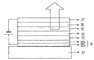
With reference to figure 3, organic luminescent device can comprise substrate 31, be positioned at anode 32 on the substrate 31, be formed on the anode 32 and receive p type hole injection layer (HIL) 33 from the hole of anode 32, be formed on the hole injection layer 33 and transporting holes to the hole transmission layer (HTL) 34 of luminescent layer (EML) 35, be formed on the hole transmission layer 34 and utilize hole and electron luminescence luminescent layer 35, be formed on the luminescent layer 35 and electronics be transferred to the electron transfer layer (ETL) 36 of luminescent layer 35 and be formed at negative electrode 37 on the electron transfer layer 36 from negative electrode 37.Hole transmission layer 34, luminescent layer 35 and electron transfer layer 36 can be made of identical or different organic material
In Fig. 3, anode 32 to hole injection layer 33, hole transmission layer 34 or luminescent layer 35, and comprises conductive layer 32a and n type organic layer 32b with hole transport.Conductive layer 32a is formed by metal, metal oxide or conducting polymer.Energy difference between the lumo energy of n type organic layer 32b and the Fermi level of conductive layer 32a is for below about 4eV.Energy difference between the lumo energy of n type organic layer 32b and the HOMO energy level of p type hole injection layer 33 is preferably below about 0.5eV for below about 1eV.Between the n of anode 32 type organic layer 32b and p type hole injection layer 33, form the NP knot.
According to another implementation of the invention, organic luminescent device can comprise substrate 31, is formed at anode 32 on the substrate 31, is formed at p type hole transmission layer 34 on the anode 32, is formed at luminescent layer 35 on the hole transmission layer 34, is formed at the electron transfer layer 36 on the luminescent layer 35 and is formed at negative electrode 37 on the electron transfer layer 36.Luminescent layer 35 and electron transfer layer 36 can be made of identical or different organic material.
According to another implementation of the invention, organic luminescent device can comprise substrate 31, is formed at anode 32 on the substrate 31, is formed at p type luminescent layer 35 on the anode 32, is formed at the electron transfer layer 36 on the luminescent layer 35 and is formed at negative electrode 37 on the electron transfer layer 36.Electron transfer layer 36 can be made of organic material.
In yet another embodiment of the present invention, when hole transmission layer 34 or luminescent layer 35 are made of p type organic material, energy difference between the HOMO energy level of the lumo energy of n type organic layer 32b and this p type hole transmission layer 34 or luminescent layer 35 is preferably below about 0.5eV for below about 1eV.Between the n of anode 32 type organic layer 32b and p type hole transmission layer 34 or p type luminescent layer 35, form the NP knot.
If the energy difference between the lumo energy of n type organic layer 32b and the Fermi level of conductive layer 32a is greater than 4eV, then surface dipole or gap state act on the effect that the energy barrier of p type hole injection layer 33 is injected in the hole and can reduce.If the energy difference between the lumo energy of n type organic layer 32b and the HOMO energy level of p type hole injection layer 33 greater than 1eV, then is not easy to form hole or electronics from p type hole injection layer 33 or n type organic layer 32b, and increased the driving voltage that the hole is injected.
In the execution mode shown in Figure 3, first electrode, organic compound layer and second electrode that comprise conductive layer and n type organic compound layer on substrate, have been stacked gradually.But, present invention resides in and stack gradually second electrode, organic compound layer on the substrate and comprise conductive layer and the reverse geometry of first electrode of n type organic compound layer.
Fig. 4 illustrates the desirable energy level of known organic light-emitting device.At this energy level, reduced the energy loss that is used for from anode and negative electrode injected hole and electronics to greatest extent.Fig. 5 shows organic light-emitting device energy level according to an illustrative embodiment of the invention.
With reference to figure 5, the organic luminescent device of another execution mode comprises anode (referring to Fig. 3), p type hole injection layer (HIL), hole transmission layer (HTL), luminescent layer (EML), electron transfer layer (ETL) and the negative electrode with conductive layer and n type organic layer according to the present invention.Energy difference between the Fermi level of the lumo energy of the n type organic layer of anode and the conductive layer of anode is for below about 4eV, and the energy difference between the HOMO energy level of the lumo energy of the n type organic layer of anode and this p type hole injection layer is for below about 1eV.Because the n type organic layer by anode has reduced the energy barrier of injected hole/electronics, so utilize the lumo energy of n type organic layer of anode and the HOMO energy level of p type hole injection layer, the hole can easily be transferred to luminescent layer from anode.
In addition, Fig. 9~15 have shown organic luminescent device according to an illustrative embodiment of the invention.
In the present invention, because the n type organic layer of anode has reduced the hole is injected into the energy barrier of p type hole injection layer, p type hole transmission layer or p type luminescent layer from anode, so the conductive layer of anode can be made of various electric conducting materials.For example, conductive layer can be used with the negative electrode identical materials and constitute.Use when constituting when anode, can prepare the organic luminescent device that electric conducting material wherein has low work content with the negative electrode identical materials.
In addition, by improve the transport property of hole and electronics with above-mentioned technical construction, the present invention can realize the balance of hole and electronics.Therefore, even do not comprise the electron injecting layer made from the material of LiF for example, compare with for example having the organic luminescent device of the electron injecting layer of LiF layer, the present invention also can realize higher device performance.At this moment, the organic compound layer that mixes with alkaline-earth metal n type can contact with second electrode.But the present invention does not get rid of from scope and comprises electron injecting layer.
Utilize mentioned above principle, the present invention can provide has high-effect and high luminiferous lamination organic luminescent device.In the lamination organic luminescent device, under same drive voltage, photism is along with the number of lamination organic luminescent device unit increases pro rata.Therefore, when organic luminescent device is lamination-type, can prepares and have high luminiferous organic luminescent device.
Another aspect of the present invention provides a kind of lamination organic luminescent device, it comprises two or more repetitives, wherein each repetitive all comprises: first electrode, the two or more organic compound layers and second electrode, first electrode comprises conductive layer and the n type organic compound layer that contacts with this conductive layer, one of organic compound layer of planting between the n of first electrode type organic compound layer and second electrode is a p type organic compound layer, its n type organic compound layer with first electrode forms the NP knot, the energy level of these layers satisfies following expression formula (1) and (2), and the one or more layers that are plugged between the p type organic compound layer and second electrode mix for using alkaline-earth metal n type:
0eV<E
nL-E
F1≤4eV (1)
E
pH-E
nL≤1eV (2)
Wherein, E
F1Be the Fermi level of the conductive layer of first electrode, E
NLBe LUMO (lowest unoccupied molecular orbital (LUMO)) energy level of the n type organic compound layer of first electrode, and E
PHFor the n type organic compound layer with first electrode forms HOMO (highest occupied molecular orbital(HOMO)) energy level of the p type organic compound layer of NP knot,
Wherein, second electrode of a repetitive is connected to first electrode of another repetitive that is connected in series with this repetitive.
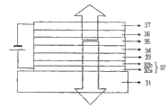
Fig. 6 shows the lamination organic luminescent device according to one embodiment of the present invention.In Fig. 6, anode (71) comprises conductive layer and n type organic compound layer.
Another aspect of the present invention provides a kind of lamination organic luminescent device, it comprises: first electrode, second electrode, be plugged on the two or more luminescence units between first electrode and second electrode, and be plugged on target between these luminescence units, wherein, first electrode comprises conductive layer and the n type organic compound layer that contacts with this conductive layer, target comprises conductive layer and the n type organic compound layer that contacts with this conductive layer, each luminescence unit all comprises the p type organic compound layer that forms the NP knot with the n type organic compound layer of first electrode or target, the energy level of these layers satisfies following expression formula (1) and (2), and each luminescence unit all further comprises the organic compound layer that mixes with alkaline-earth metal n type:
0eV<E
nL-E
F1≤4eV (1)
E
pH-E
nL≤1eV (2)
Wherein, E
F1Be the Fermi level of the conductive layer of first electrode or target, E
NLBe LUMO (lowest unocccupied molecular orbital) energy level of the n type organic compound layer of first electrode or target, and E
PHForm HOMO (highest occupied molecular orbital(HOMO)) energy level of the p type organic compound layer of NP knot for n type organic compound layer with first electrode or target.
In the present invention, as mentioned above,, can prepare the lamination organic luminescent device of the Fig. 7 that is equal to structure shown in Figure 6 because negative electrode and anode can be made of same material.With reference to figure 7, lamination organic light-emitting device structure according to the present invention is as follows: the wherein stacked a plurality of organic layer 83 between anode 81 and the negative electrode 87 and repetitives of target conductive layer 85 of being inserted in.Anode 81 and intermediate electrode layer 85 comprise conductive layer and n type organic layer.Preferably, conductive layer is made of transparent material, and work content and transmission of visible light that its work content is similar to the material of negative electrode 87 are more than 50%.Using under the situation of opaque metal as conductive, conductive layer need made enough thin so that conductive layer is transparent.The example of opaque metal can comprise Al, Ag, Cu, Ca, Mg, MgAg, CaAg etc.Particularly, when the Al metal formed the conductive layer of middle motor layer 85, the thickness of conductive layer was about 5~10nm, but is not limited to these.In lamination organic luminescent device according to the present invention, be included in the conductive layer in the target, can be extremely thin film, for example
 More preferably

In the lamination organic luminescent device, describe identical with above-mentioned to organic light-emitting device with a unit about the explanation of electrode and various organic compound layers.
Below, will describe each layer of organic light-emitting device that constitutes according to the embodiment of the present invention in detail.Each that describes below layer can be formed by homogenous material or two or more mixtures of material.
Anode
Anode injects p type organic layer, for example hole injection layer, hole transmission layer or luminescent layer with the hole.Anode comprises conductive layer and n type organic layer.Conductive layer comprises metal, metal oxide or conducting polymer.Conducting polymer can comprise electric conducting polymer.
Conductive layer because n type organic layer has reduced the hole is injected into the energy barrier of p type organic layer from first electrode, so can be formed by various electric conducting materials.For example, conductive layer has the Fermi level that is about 2~5.5eV.In conventional organic luminescent device, having only Fermi level is that the material of 5~6eV just can be used for anode.But in the present invention, Fermi level is that the material of 2~5eV, particularly Fermi level are that the material of 2~4eV can be used for anode.Examples of conductive materials comprises carbon, caesium, potassium, lithium, calcium, sodium, magnesium, zirconium, indium, aluminium, silver, tantalum, vanadium, chromium, copper, zinc, iron, tungsten, molybdenum, nickel, gold, other metal and their alloy; Zinc oxide, indium oxide, tin oxide, tin indium oxide (ITO), indium zinc oxide and with they similar metal oxides; And the mixture of oxide and metal, for example ZnO:Al and SnO
2: Sb.At organic luminescent device is when pushing up to emission type, and opaque material and transparent material with excellent reflection can be as the materials of conductive layer.Under emission type organic light-emitting device situation, must use transparent material the end of at as conductive.If use opaque material, this layer must be made enough thin so that this layer is for almost transparent.In order to regulate the Fermi level of conductive layer, the surface that can handle conductive layer with nitrogen gas plasma or oxygen gas plasma.
Handling then by oxygen gas plasma with the Fermi level of the conductive layer of plasma treatment increases, and it then reduces by nitrogen plasma treatment.
In addition, nitrogen gas plasma increases the conductivity of conductive layer, reduces lip-deep oxygen concentration, and generates nitride from the teeth outwards, has increased the life-span of device thus.But nitrogen plasma know from experience to reduce the Fermi level of conductive layer, and making the injection deterioration in hole increases driving voltage thus.
When n type organic compound layer used according to the invention with when using the method for NP knot, even because the Fermi level of character conductive layer is injected in the hole that the NP knot causes reduces also unaffected.Therefore, in the present invention, nitrogen gas plasma can be implemented, and can realize the device of long-life and low-voltage thus.
N type organic layer is plugged between conductive layer and the p type organic layer, and in low electric field p type organic layer is injected in the hole.Select n type organic layer so that the energy difference between the Fermi level of the conductive layer of the lumo energy of the n type organic layer of anode and anode for below about 4eV, and to make the energy difference between the HOMO energy level of the lumo energy of n type organic layer and p type organic layer be below about 1eV.
For example, the lumo energy of n type organic layer is about 4~7eV, and its electron mobility is about 10
-8Cm
2/ Vs~1cm
2/ Vs, and more preferably 10
-6Cm
2/ Vs~10
-3Cm
2/ Vs.If electron mobility is less than 10
-8Cm
2/ Vs then is not easy the hole is injected into p type organic layer from n type organic layer.If electron mobility is greater than 1cm
2/ Vs then can carry out the hole effectively and inject.But, in the case, because this layer is formed by the crystallization organic material usually, so be difficult to this layer is applied in the organic luminescent device that adopts the amorphous organic material.
N type organic layer can be by can maybe being used the film forming material of solution process to form by vacuum moulding machine.The example of n type organic material comprises, but be not limited to: 2,3,5,6-tetrafluoro-7,7,8,3,4 of 8-four cyanogen quinone bismethanes (F4TCNQ), fluorine replacement, 9, NTCDA and six nitriles, six azepine benzophenanthrenes (HAT) that the NTCDA that the PTCDA that 10-perylene tetracarboxylic dianhydride (PTCDA), cyano group replace, naphthalene tetracarboxylic acid dianhydride (NTCDA), fluorine replace, cyano group replace.
Hole injection layer (HIL) or hole transmission layer (HTL)
Hole injection layer or hole transmission layer can be formed by the p type organic layer that is plugged between anode and the negative electrode.Because p type hole injection layer or p type hole transmission layer and n type organic layer form the NP knot, because the hole that the NP knot forms is transferred to luminescent layer by this p type hole injection layer or p type hole transmission layer.
Energy difference between the lumo energy of the HOMO energy level of p type hole injection layer or p type hole transmission layer and n type organic layer is below about 1eV, and is preferably below about 0.5eV.The example of p type hole injection layer or p type hole transmission layer comprises, but is not limited to, based on compound, the conducting polymer of arylamine or the block copolymer that has conjugate moiety and non-conjugated part simultaneously.
Luminescent layer (EML)
In luminescent layer, hole transport and electric transmission take place simultaneously.Therefore, luminescent layer can have n type and p type characteristic simultaneously.For simplicity, under the fast situation of electron transmission efficiency hole transport, luminescent layer can be defined as n type luminescent layer, and under the hole transport situation faster, luminescent layer can be defined as p type luminescent layer than electric transmission.
In n type luminescent layer, because the electron transmission efficiency hole transport is fast, so the generation of the interface between hole transmission layer and luminescent layer is luminous.Therefore, if the lumo energy of hole transmission layer is higher than the lumo energy of luminescent layer, then can guarantee higher luminous efficiency.The example of n type luminescent layer comprises, but is not limited to three (oxine) aluminium (Alq
3); Oxine beryllium (BAlq); Based on the compound of benzoxazole, based on the compound of benzothiazole or based on the compound of benzimidazole; Compound based on poly-fluorenes; And based on the compound of sila cyclopentadiene (silole).
In p type luminescent layer, hole transport is faster than electric transmission, and is therefore, luminous in the near interface generation of electron transfer layer and luminescent layer.Therefore, if the HOMO energy level of electron transfer layer is lower than the HOMO energy level of luminescent layer, then can guarantee higher luminous efficiency.
Under the situation of using p type luminescent layer, to compare with the situation of using n type luminescent layer, the effect of the increase luminous efficiency that is obtained by the lumo energy that changes hole transmission layer is less.Therefore, under the situation of using p type luminescent layer, can prepare between n type organic compound layer and p type luminescent layer and have the organic luminescent device of NP junction structure, and need not use hole injection layer and hole transmission layer.P type luminescent layer comprises, but is not limited to, based on the compound of carbazole, based on the compound of anthracene, based on poly-polymer or spiro-compound to styrene (PPV).
Electron transfer layer (ETL)
As the material that is used for electron transfer layer, the preferred material that has more big electron mobility that uses so that from negative electrode accept electronics and with electric transmission to luminescent layer.The example of electron transfer layer comprises, but is not limited to three (oxine) aluminium (Alq
3), comprise Alq
3The organic compound of structure or flavonol-metal complex or based on the compound of sila cyclopentadiene (silole).
Negative electrode
As the material that is used for negative electrode, the preferred material that uses low work content is so that easily be injected into organic compound layer, for example electron transfer layer with electronics.When using the electron transfer layer of using alkaline earth metal doping, work content (Fermi level) can be used for negative electrode for the following material of 6.0eV.Negative electrode comprises, but is not limited to, metal, for example magnesium, calcium, sodium, potassium, titanium, indium, yttrium, lithium, gadolinium, aluminium, silver, tin, nickel, gold, molybdenum, iron and lead, or their alloy; Multilayer material, for example LiF/Al or LiO
2/ Al; And metal oxide, for example ITO, IZO etc.Negative electrode can be formed by the conductive layer identical materials with anode.Perhaps, the conductive layer of negative electrode or anode can comprise transparent material.
The invention execution mode
Down the present invention may be better understood in the enlightenment of embodiment below, these embodiment the present invention that is used to explain, and should not be construed as restriction the present invention.
<embodiment 〉
Utilize UPS and UV-VIS absorption process to measure HOMO energy level and the lumo energy of HAT.
Six nitriles, six azepine benzophenanthrenes (HAT) are as the organic material with n N-type semiconductor N characteristic.In order to measure the HOMO energy level of HAT, use UPS (UV photoelectron spectroscopy) method.In the method, when from the vacuum UV ray (21.20eV) of He lamp emission at ultravacuum environment (<10
-8Holder) in when shining on the sample, analyzes the kinetic energy of the electronics that discharges from sample,, perhaps detect the ionization energy of organic material, i.e. HOMO energy level and Fermi level to detect the work content of metal.That is to say that the kinetic energy of the electronics that discharges from sample is the difference between vacuum UV energy 21.2eV and the electron binding energy of wanting measuring samples when vacuum UV ray (21.20eV) shines on the sample.Therefore, the binding energy of molecule distributes and can obtain by the kinetic energy distribution of analyzing the electronics that discharges from sample in specimen material.Relevant is that under the maximized situation of the kinetic energy that makes electronics, the binding energy of sample has minimum value therewith.Thus, can determine the work content (Fermi level) and the HOMO energy level of sample.
In this embodiment, use golden film to measure golden work content, and when being deposited on the HAT material on the golden film,, measure the HOMO energy level of HAT by analyzing the kinetic energy of the electronics that discharges from the HAT material.It is the UPS data that the HAT film of 20nm obtains that Fig. 8 illustrates by golden film and the thickness on golden film.Below, will adopt people such as H.Ishii, Advanced Materials, 11, disclosed term is described among the 605-625 (1999).
In Fig. 8, calculate the binding energy of x-axle based on the work content of measuring from golden film.That is to say, in measurement, measured golden work content, and find that it is 5.28eV, this is to obtain by the maximum (15.92eV) that deducts binding energy from the energy (21.20eV) of radiant light.The HOMO energy level of HAT by deducting binding energy the luminous energy on being radiated the HAT that is deposited on the golden film maximum (15.21eV) and the difference between the minimum value (3.79eV) obtain, it is 9.78eV, and Fermi level is 6.02V.
Employing has obtained another UV-VIS spectrum by HAT being deposited on the organic material that obtains on the glass surface, and analyzes the ABSORPTION EDGE edge, finds that spectrum has the band gap of about 3.26eV.Thus, as can be seen, the LUMO of HAT is about 6.54eV.This value can change by the exciton binding energy of HAT material.That is to say that as can be seen, 6.54eV is greater than the Fermi level (6.02eV) of above-mentioned material.Exciton binding energy is necessary for more than the 0.52eV, so that lumo energy is less than Fermi level.Because the exciton binding energy level of organic material is generally 0.5~1eV, can expect that the lumo energy of HAT is 5.54~6.02eV.
On glass substrate, using sputter to form thickness is 1000
IZO (indium zinc oxide) conductive layer, then by heating HAT of vacuum moulding machine formula 2-1 on the IZO layer, to thickness be about 500
 The transparent anode that has IZO conductive layer and n type organic layer with formation.The HOMO energy level of HAT is about 9.78eV.Subsequently, by the NPB of heating, vacuum sedimentation type 2-2, forming thickness thus is about 400
 P type hole transmission layer.Alq by heating vacuum moulding machine formula 2-3 on this p type hole transmission layer
3(HOMO energy level=about 5.7eV), the C545T dopant of the formula 2-4 of the 6 volume % that mix simultaneously is to about 300
P type hole transmission layer.Alq by heating vacuum moulding machine formula 2-3 on this p type hole transmission layer
3(HOMO energy level=about 5.7eV), the C545T dopant of the formula 2-4 of the 6 volume % that mix simultaneously is to about 300
 Thickness, to form luminescent layer.
The Mg of 30 volume % is doped in the compound of formula 2-5, and on luminescent layer, is deposited into 200 by heating, vacuum
 Thickness, to form electron transfer layer.Vacuum moulding machine thickness is 1000 on the electron transfer layer that mixes subsequently
Aluminium lamination, to form negative electrode, make organic luminescent device thus.In above-mentioned steps, the deposition rate of organic material is maintained at about 0.4~0.7
Thickness, to form electron transfer layer.Vacuum moulding machine thickness is 1000 on the electron transfer layer that mixes subsequently
Aluminium lamination, to form negative electrode, make organic luminescent device thus.In above-mentioned steps, the deposition rate of organic material is maintained at about 0.4~0.7
 / second, and the deposition rate of aluminium is maintained at about 2
/ second.In deposition process, the vacuum degree of settling chamber is maintained at about 2 * 10
-7~5 * 10
-8Holder.
/ second, and the deposition rate of aluminium is maintained at about 2
/ second.In deposition process, the vacuum degree of settling chamber is maintained at about 2 * 10
-7~5 * 10
-8Holder.
[formula 2-1] [formula 2-2]

[formula 2-3] [formula 2-4]

[formula 2-5]
Embodiment 3
Except electron transfer layer replaces Mg mixes with the Ca of 10 volume %, adopt the method identical to prepare organic luminescent device with embodiment 2.
Embodiment 4
On glass substrate, use heat deposition method formation thickness to be
 The aluminium conductive layer, then by heating HAT of vacuum moulding machine formula 2-1 on aluminium lamination, to thickness for approximately
 The reflection anode that has aluminium conductive layer and n type organic layer with formation.Subsequently, by the NPB of heating, vacuum sedimentation type 2-2, form thickness thus for about
 P type hole transmission layer.Alq by heating vacuum moulding machine formula 2-3 on this p type hole transmission layer
3(HOMO energy level=about 5.7eV), the C545T dopant of the formula 2-4 of the 6 volume % that mix simultaneously is to about
P type hole transmission layer.Alq by heating vacuum moulding machine formula 2-3 on this p type hole transmission layer
3(HOMO energy level=about 5.7eV), the C545T dopant of the formula 2-4 of the 6 volume % that mix simultaneously is to about
 Thickness, to form luminescent layer.
The Ca of 10 volume % is doped in the compound of formula 2-5, and on luminescent layer, is deposited into by heating, vacuum
 Thickness, to form electron transfer layer.Vacuum moulding machine thickness is on the electron transfer layer that mixes subsequently
 The Ca layer, to form semitransparent cathode, make organic luminescent device thus.In above-mentioned steps, the deposition rate of organic material is maintained at approximately
 Second, and the deposition rate of aluminium is maintained at approximately
 / second.In deposition process, the vacuum degree of settling chamber is maintained at about 2 * 10
-7~5 * 10
-8Holder.
/ second.In deposition process, the vacuum degree of settling chamber is maintained at about 2 * 10
-7~5 * 10
-8Holder.
Embodiment 5
Except on glass substrate, use heat deposition method formation thickness to be
The Ag conductive layer, the HAT by heating vacuum moulding machine formula 2-1 on the Ag conductive layer is to approximately then
 Thickness have with formation beyond the reflection anode of Ag conductive layer and n type organic layer, prepare organic luminescent device with the method identical with embodiment 4.
Embodiment 6
Except on glass substrate, use heat deposition method formation thickness to be
 The Ca conductive layer, the HAT by heating vacuum moulding machine formula 2-1 on the Ca conductive layer is to approximately then
 Thickness have with formation beyond the reflection anode of Ca conductive layer and n type organic layer, prepare organic luminescent device with the method identical with embodiment 4.
Embodiment 7
On glass substrate, use sputter formation thickness to be
 IZO (indium zinc oxide) negative electrode.Then, the Ca of 10 volume % is doped in the compound of formula 2-5, and on the IZO layer, is deposited into by heating, vacuum
 Thickness, to form electron transfer layer.Alq by heating vacuum moulding machine formula 2-3 on this electron transfer layer
3, the C545T dopant of the formula 2-4 of the 6 volume % that mix simultaneously is to about
Thickness, to form electron transfer layer.Alq by heating vacuum moulding machine formula 2-3 on this electron transfer layer
3, the C545T dopant of the formula 2-4 of the 6 volume % that mix simultaneously is to about
 Thickness, to form luminescent layer.On luminescent layer,, form thickness thus for about by the NPB of heating, vacuum sedimentation type 2-2
 P type hole transmission layer.HAT by heating vacuum moulding machine formula 2-1 on this p type hole transmission layer is extremely about
 Thickness, use the sputter deposit thickness to be approximately thereon
 IZO (indium zinc oxide) conductive layer, have the transparent anode of IZO layer and HAT n type organic layer with formation.The HOMO energy level of HAT is about 9.78eV.In above-mentioned steps, the deposition rate of organic material is maintained at approximately
 / second, and the deposition rate of IZO is maintained at approximately
 Second.In deposition process, the vacuum degree of settling chamber is maintained at about 2 * 10
-7~5 * 10
-8Holder.
Second.In deposition process, the vacuum degree of settling chamber is maintained at about 2 * 10
-7~5 * 10
-8Holder.
Embodiment 8
On glass substrate, use sputter formation thickness to be
 IZO (indium zinc oxide) negative electrode.Then, the Ca of 10 volume % is doped in the compound of formula 2-5, and on the IZO layer, is deposited into by heating, vacuum
 Thickness, to form electron transfer layer.Alq by heating vacuum moulding machine formula 2-3 on this electron transfer layer
3, the C545T dopant of the formula 2-4 of the 6 volume % that mix simultaneously is to about
Thickness, to form electron transfer layer.Alq by heating vacuum moulding machine formula 2-3 on this electron transfer layer
3, the C545T dopant of the formula 2-4 of the 6 volume % that mix simultaneously is to about
 Thickness, to form luminescent layer.On luminescent layer,, form thickness thus for about by the NPB of heating, vacuum sedimentation type 2-2
 P type hole transmission layer.HAT by heating vacuum moulding machine formula 2-1 on this p type hole transmission layer is extremely about
 Thickness, deposit thickness is for approximately thereon
 The Al conductive layer, have the anode of Al layer and HAT n type organic layer with formation.In above-mentioned steps, the deposition rate of organic material is maintained at approximately
 / second, and the deposition rate of IZO is maintained at approximately
 / second.In deposition process, the vacuum degree of settling chamber is maintained at about 2 * 10
-7~5 * 10
-8Holder.
/ second.In deposition process, the vacuum degree of settling chamber is maintained at about 2 * 10
-7~5 * 10
-8Holder.
Embodiment 9
On glass substrate, use sputter formation thickness to be
 IZO (indium zinc oxide) negative electrode.Then, the Ca of 10 volume % is doped in the compound of formula 2-5, and on the IZO layer, is deposited into by heating, vacuum
 Thickness, to form electron transfer layer.Alq by heating vacuum moulding machine formula 2-3 on this electron transfer layer
3, the C545T dopant of the formula 2-4 of the 6 volume % that mix simultaneously is to about
Thickness, to form luminescent layer.On luminescent layer,, form thickness thus for about by the NPB of heating, vacuum sedimentation type 2-2
Thickness, to form electron transfer layer.Alq by heating vacuum moulding machine formula 2-3 on this electron transfer layer
3, the C545T dopant of the formula 2-4 of the 6 volume % that mix simultaneously is to about
Thickness, to form luminescent layer.On luminescent layer,, form thickness thus for about by the NPB of heating, vacuum sedimentation type 2-2
 P type hole transmission layer.HAT by heating vacuum moulding machine formula 2-1 on this p type hole transmission layer is extremely about
 Thickness, deposit thickness is for approximately thereon
 The Ag conductive layer, have the anode of Ag conductive layer and HAT n type organic layer with formation.In above-mentioned steps, the deposition rate of organic material is maintained at approximately
 / second, and the deposition rate of IZO is maintained at approximately
 / second.In deposition process, the vacuum degree of settling chamber is maintained at about 2 * 10
-7~5 * 10
-8Holder.
/ second.In deposition process, the vacuum degree of settling chamber is maintained at about 2 * 10
-7~5 * 10
-8Holder.
Embodiment 10
On glass substrate, use sputter formation thickness to be
IZO (indium zinc oxide) negative electrode.Then, the Ca of 10 volume % is doped in the compound of formula 2-5, and on the IZO layer, is deposited into by heating, vacuum
 Thickness, to form electron transfer layer.Alq by heating vacuum moulding machine formula 2-3 on this electron transfer layer
3, the C545T dopant of the formula 2-4 of the 6 volume % that mix simultaneously is to about
Thickness, to form electron transfer layer.Alq by heating vacuum moulding machine formula 2-3 on this electron transfer layer
3, the C545T dopant of the formula 2-4 of the 6 volume % that mix simultaneously is to about
 Thickness, to form luminescent layer.On luminescent layer,, form thickness thus for about by the NPB of heating, vacuum sedimentation type 2-2
 P type hole transmission layer.HAT by heating vacuum moulding machine formula 2-1 on this p type hole transmission layer is extremely about
 Thickness, deposit thickness is for approximately thereon
The Ca conductive layer, have the anode of Ca conductive layer and HAT n type organic layer with formation.In above-mentioned steps, the deposition rate of organic material is maintained at approximately
Thickness, deposit thickness is for approximately thereon
The Ca conductive layer, have the anode of Ca conductive layer and HAT n type organic layer with formation.In above-mentioned steps, the deposition rate of organic material is maintained at approximately
 / second, and the deposition rate of IZO is maintained at approximately
 / second.In deposition process, the vacuum degree of settling chamber is maintained at about 2 * 10
-7~5 * 10
-8Holder.
/ second.In deposition process, the vacuum degree of settling chamber is maintained at about 2 * 10
-7~5 * 10
-8Holder.
Embodiment 11
Except on glass substrate, use heat deposition instrument formation thickness to be
The aluminium reflective cathode beyond, adopt the method identical to prepare organic luminescent device with embodiment 7.
Embodiment 12
On glass substrate, use sputter formation thickness to be
 IZO (indium zinc oxide) cathode layer.Then, the Ca of 10 volume % is doped in the compound of formula 2-5, and on the IZO layer, is deposited into by heating, vacuum
 Thickness, to form electron transfer layer.Alq by heating vacuum moulding machine formula 2-3 on this electron transfer layer
3, the C545T dopant of the formula 2-4 of the 6 volume % that mix simultaneously is to about
Thickness, to form luminescent layer.On luminescent layer,, form thickness thus for about by the NPB of heating, vacuum sedimentation type 2-2
Thickness, to form electron transfer layer.Alq by heating vacuum moulding machine formula 2-3 on this electron transfer layer
3, the C545T dopant of the formula 2-4 of the 6 volume % that mix simultaneously is to about
Thickness, to form luminescent layer.On luminescent layer,, form thickness thus for about by the NPB of heating, vacuum sedimentation type 2-2
 P type hole transmission layer.HAT by heating vacuum moulding machine formula 2-1 on this p type hole transmission layer is extremely about
 Thickness, deposit thickness is for approximately thereon
 The Ca conductive layer, have the transparent target of Ca layer and HAT n type organic layer with formation.The Ca of 10 volume % is doped in the compound of formula 2-5, and on target, is deposited into by heating, vacuum
 Thickness, to form electron transfer layer.Alq by heating vacuum moulding machine formula 2-3 on this electron transfer layer
3, the C545T dopant of the formula 2-4 of the 6 volume % that mix simultaneously is to about
Thickness, to form electron transfer layer.Alq by heating vacuum moulding machine formula 2-3 on this electron transfer layer
3, the C545T dopant of the formula 2-4 of the 6 volume % that mix simultaneously is to about
 Thickness, to form luminescent layer.On luminescent layer,, form thickness thus for about by the NPB of heating, vacuum sedimentation type 2-2
P type hole transmission layer.HAT by heating vacuum moulding machine formula 2-1 on this p type hole transmission layer is extremely about
Thickness, use the sputter deposit thickness to be approximately thereon
Thickness, to form luminescent layer.On luminescent layer,, form thickness thus for about by the NPB of heating, vacuum sedimentation type 2-2
P type hole transmission layer.HAT by heating vacuum moulding machine formula 2-1 on this p type hole transmission layer is extremely about
Thickness, use the sputter deposit thickness to be approximately thereon
 IZO (indium zinc oxide) conductive layer, have the transparent anode of IZO layer and HAT n type organic layer with formation, preparation has the transparent lamination organic luminescent device of reverse geometry thus.The HOMO energy level of HAT is about 9.78eV.In above-mentioned steps, the deposition rate of organic material is maintained at approximately
 Second, and the deposition rate of IZO is maintained at approximately
 / second.In deposition process, the vacuum degree of settling chamber is maintained at about 2 * 10
-7~5 * 10
-8Holder.
/ second.In deposition process, the vacuum degree of settling chamber is maintained at about 2 * 10
-7~5 * 10
-8Holder.
Comparing embodiment 1
Except electron transfer layer does not have doped with Mg, this layer uses the compound (HOMO=5.7eV and LUMO=2.8eV) of formula 2-5 to be formed up to
 Thickness, and order vacuum moulding machine thickness is on electron transfer layer
 Lithium fluoride (LiF) film and thickness be
Aluminium lamination to form beyond the negative electrode, the step that repeats
Lithium fluoride (LiF) film and thickness be
Aluminium lamination to form beyond the negative electrode, the step that repeats embodiment 2 prepares organic luminescent device.In above-mentioned steps, the deposition rate of organic material is maintained at approximately
/ second, the deposition rate of LiF is maintained at approximately
/ second, and the deposition rate of aluminium is maintained at approximately
 / second.In deposition process, the vacuum degree of settling chamber is maintained at about 2 * 10
-7~5 * 10
-8Holder.
/ second.In deposition process, the vacuum degree of settling chamber is maintained at about 2 * 10
-7~5 * 10
-8Holder.
Comparing embodiment 2
On glass substrate, use sputter formation thickness to be
 IZO (indium zinc oxide) anode, subsequently,, form thickness thus for approximately by the NPB of heating, vacuum sedimentation type 2-2
 Hole transmission layer.Alq by heating vacuum moulding machine formula 2-3 on this hole transmission layer
3(HOMO energy level=about 5.7eV), the C545T dopant of the formula 2-4 of the 6 volume % that mix simultaneously is to about
Hole transmission layer.Alq by heating vacuum moulding machine formula 2-3 on this hole transmission layer
3(HOMO energy level=about 5.7eV), the C545T dopant of the formula 2-4 of the 6 volume % that mix simultaneously is to about
 Thickness, to form luminescent layer.
The Ca of 10 volume % is doped in the compound of formula 2-5, and on luminescent layer, is deposited into by heating, vacuum
 Thickness, to form electron transfer layer.Vacuum moulding machine thickness is on the electron transfer layer that mixes subsequently
 Aluminium lamination, to form negative electrode, make organic luminescent device thus.In above-mentioned steps, the deposition rate of organic material is maintained at approximately
 / second, and the deposition rate of aluminium is maintained at approximately
 / second.In deposition process, the vacuum degree of settling chamber is maintained at about 2 * 10
-7~5 * 10
-8Holder.
/ second.In deposition process, the vacuum degree of settling chamber is maintained at about 2 * 10
-7~5 * 10
-8Holder.
[table 1]

As can be seen from Table 1, compare with the device that has LiF rather than have a comparing embodiment 1 of alkaline earth metal doping layer, the device that has with the electron transfer layer of alkaline earth metal doping has low driving voltage and high efficiency.By embodiment 2 and 3 as can be seen, when electron transfer layer during with the alkaline earth metal doping of Mg for example and Ca, electronics can be injected from the Al electrode effectively.
By comparing embodiment 1 and 2 as can be seen, during technology in only adopting NP knot and n type doping organic compound layer, driving voltage increases and the photism reduction.Particularly, by the comparing embodiment 2 that only adopts n type organic compound layer as can be seen,, the hole causes significantly having increased driving voltage because injecting the reduction of character.
Embodiment 4,5 and 6 provides the end to luminescent device, and wherein use has the conductive of the reflective metals of low Fermi level as the anode of the luminescent device with normal configuration.In embodiment 4~6, driving voltage is below the 3.6V, is lower than the driving voltage of comparing embodiment 1.This shows that when using n type compound to form the NP knot, the material that can use low Fermi level is as anode conductive layer.Photism according to the device of embodiment 4~6 is relatively low, because use translucent Ca electrode as negative electrode, wherein the Ca electrode can absorbing light.
In embodiment 7, prepared transparent OLED with reverse geometry, it has the NP junction structure that adopts n type organic compound and with the electron transfer layer of alkaline earth metal doping.The anode of this device and negative electrode all are the transparency electrodes that forms with IZO.By embodiment 7 as can be seen, when electron transfer layer mixes with the alkaline-earth metal (calcium) of 10 volume %, can effectively electronics be injected electron transfer layer from the IZO negative electrode.
In embodiment 8,9 and 10, adopt respectively Al (4.2eV), Ag (4.2eV) with low Fermi level and Ca (2.6eV) metal as anode preparation have reverse geometry the top to luminescent device, it has the NP junction structure that adopts n type organic compound and with the electron transfer layer of alkaline-earth metal (Ca) doping of 10 volume %.The IZO (5.0eV) that has high Fermi level with use is similar as the embodiment 4 of anode, in embodiment 8-10, has recorded luminosity and also recorded 900cd/m under low driving voltage
2Above high photism.In addition, as can be seen, in device, can use metal electrode as anode with low Fermi level with the NP knot that uses n type organic compound.
In embodiment 11, prepared have reverse geometry the end to luminescent device, its use transparent IZO as anode and Al as negative electrode, this device demonstrates low driving voltage and high photism.
In embodiment 12, prepared an example of transparent laminated device with reverse geometry, it uses IZO transparent cathode, translucent Ca target and IZO transparent anode conductive layer.By embodiment 12 as can be seen, compare with single unit component, driving voltage has increased twice, but photism is compared also with single cell transparent device and increased more than the twice.As can be seen, in laminated device, be used as the Ca electrode of target as anode and negative electrode operational excellence.
As can be seen from the above-described embodiment, when the organic compound layer of the NP knot of employing used according to the invention n type organic compound layer and the doping of n type, out of use material in routine techniques with low Fermi level, for example Ca, Al, Ag, Mg etc., can be used as anode material, and have the material of high Fermi level, for example IZO, ITO etc., can be used as cathode material, because the restriction of the Fermi level of antianode and negative electrode has been relaxed.Therefore, as can be seen from the above-described embodiment, when the restriction of the Fermi level that relaxes antianode and negative electrode, can prepare various types of organic luminescent devices, for example normal configuration, reverse geometry, top to luminous, the end to luminous, two-way luminous etc.
Claims (28)
1. organic luminescent device, it comprises: first electrode, the two or more organic compound layers and second electrode, wherein, first electrode comprises conductive layer and the n type organic compound layer that contacts with this conductive layer, one of organic compound layer of planting between the n of first electrode type organic compound layer and second electrode forms the p type organic compound layer of NP knot for the n type organic compound layer with first electrode, the energy level of these layers satisfies following expression formula (1) and (2), and the one or more layers that are plugged between the p type organic compound layer and second electrode mix for using alkaline-earth metal n type:
0eV<E
nL-E
F1≤4eV (1)
E
pH-E
nL≤1eV (2)
Wherein, E
F1Be the Fermi level of the conductive layer of first electrode, E
NLBe LUMO (lowest unoccupied molecular orbital (LUMO)) energy level of the n type organic compound layer of first electrode, and E
PHForm HOMO (highest occupied molecular orbital(HOMO)) energy level of the p type organic compound layer of NP knot for n type organic compound layer with first electrode.
2. organic luminescent device according to claim 1, wherein, the described organic compound layer that mixes with alkaline-earth metal n type is that electron injecting layer, electron transfer layer or electronics inject and transport layer.
3. organic luminescent device according to claim 1, wherein, the described organic compound layer that mixes with alkaline-earth metal n type contacts with described second electrode.
4. organic luminescent device according to claim 1, wherein, the structure that described organic luminescent device has is for stacking gradually first electrode, organic compound layer and second electrode with from the bottom up order on substrate.
5. organic luminescent device according to claim 1, wherein, the structure that described organic luminescent device has is for stacking gradually second electrode, organic compound layer and first electrode with from the bottom up order on substrate.
6. organic luminescent device according to claim 1, wherein, described p type organic compound layer is hole injection layer, hole transmission layer or luminescent layer.
7. organic luminescent device according to claim 1, its comprise further that one deck at least is plugged on described p type organic compound layer and the organic compound layer that mixes with alkaline-earth metal n type between or at organic compound layer that mixes with alkaline-earth metal n type and the organic compound layer between described second electrode.
8. organic luminescent device according to claim 1, wherein, the n type organic compound layer of described first electrode is formed by following a kind of organic material, described organic material is selected from: 2,3,5,6-tetrafluoro-7,7,8,3,4 of 8-four cyanogen quinone bismethanes (F4TCNQ), fluorine replacement, 9, NTCDA and six nitriles, six azepine benzophenanthrenes (HAT) that the NTCDA that the PTCDA that 10-perylene tetracarboxylic dianhydride (PTCDA), cyano group replace, naphthalene tetracarboxylic acid dianhydride (NTCDA), fluorine replace, cyano group replace.
9. organic luminescent device according to claim 1, wherein, the conductive layer of described first electrode is formed by following material, and described material is selected from metal, metal oxide and conducting polymer.
10. organic luminescent device according to claim 1, wherein, the conductive layer of described first electrode and second electrode are formed by identical materials.
11. organic luminescent device according to claim 1, wherein, at least one in the conductive layer of described first electrode and second electrode comprises transparent material.
12. organic luminescent device according to claim 1, wherein, the lumo energy of described n type organic compound layer is about 4~7eV, and electron mobility is about 10
-8Cm
2/ Vs~1cm
2/ Vs.
13. organic luminescent device according to claim 1, wherein, described alkaline-earth metal comprises and is selected from calcium (Ca), strontium (Sr), barium (Ba), radium (Ra), beryllium (Be) and the magnesium (Mg) one or more.
14. organic luminescent device according to claim 1, wherein, in the organic compound layer that mixes with alkaline-earth metal n type, doping content is 0.02~50 volume %.
15. one kind prepares the organic light-emitting device method, described organic luminescent device comprises first electrode, two or more organic compound layer and second electrode, wherein, described method comprises: form n type organic compound layer and make this n type organic compound layer contact with conductive layer to form first electrode on conductive layer; On the n of first electrode type organic compound layer, form p type organic compound layer so that this p type organic compound layer contacts with n type organic compound layer; Above p type organic compound layer, form the organic compound layer that mixes with alkaline-earth metal n type; And formation second electrode makes this second electrode contact with the organic compound layer that mixes with alkaline-earth metal n type on the organic compound layer that mixes with alkaline-earth metal n type, and wherein the energy level of these layers satisfies following expression formula (1) and (2):
0eV<E
nL-E
F1≤4eV (1)
E
pH-E
nL≤1eV (2)
Wherein, E
F1Be the Fermi level of the conductive layer of first electrode, E
NLBe LUMO (lowest unoccupied molecular orbital (LUMO)) energy level of the n type organic compound layer of first electrode, and E
PHForm HOMO (highest occupied molecular orbital(HOMO)) energy level of the p type organic compound layer of NP knot for n type organic compound layer with first electrode.
16. method according to claim 15, it further comprises, forms organic compound layer forming described p type organic compound layer and form between the described organic compound layer with the doping of alkaline-earth metal n type.
17. one kind prepares the organic light-emitting device method, described organic luminescent device comprises second electrode, two or more organic compound layer and first electrode, and wherein, described method comprises: form second electrode; Forming the organic compound layer that mixes with alkaline-earth metal n type on second electrode makes the organic compound layer of this n type doping contact with second electrode; Above organic compound layer that the n type mixes, form p type organic compound layer; On p type organic compound layer, form n type organic compound layer so that this n type organic compound layer contacts with p type organic compound layer, and the formation conductive layer makes this conductive layer contact to form first electrode with n type organic compound layer on n type organic compound layer, and wherein the energy level of these layers satisfies following expression formula (1) and (2):
0eV<E
nL-E
F1≤4eV (1)
E
pH-E
nL≤1eV (2)
Wherein, E
F1Be the Fermi level of the conductive layer of first electrode, E
NLBe LUMO (lowest unoccupied molecular orbital (LUMO)) energy level of the n type organic compound layer of first electrode, and E
PHForm HOMO (highest occupied molecular orbital(HOMO)) energy level of the p type organic compound layer of NP knot for n type organic compound layer with first electrode.
18. method according to claim 17, it further comprises, form described with the doping of alkaline-earth metal n type organic compound layer and form between the described p type organic compound layer and form organic compound layer.
19. lamination organic luminescent device, it comprises two or more repetitives, wherein each repetitive all comprises: first electrode, the two or more organic compound layers and second electrode, first electrode comprises conductive layer and the n type organic compound layer that contacts with this conductive layer, one of organic compound layer of planting between the n of first electrode type organic compound layer and second electrode is a p type organic compound layer, its n type organic compound layer with first electrode forms the NP knot, the energy level of these layers satisfies following expression formula (1) and (2), and the one or more layers that are plugged between the p type organic compound layer and second electrode mix for using alkaline-earth metal n type:
0eV<E
nL-E
F1≤4eV (1)
E
pH-E
nL≤1eV (2)
Wherein, E
F1Be the Fermi level of the conductive layer of first electrode, E
NLBe LUMO (lowest unoccupied molecular orbital (LUMO)) energy level of the n type organic compound layer of first electrode, and E
PHFor the n type organic compound layer with first electrode forms HOMO (highest occupied molecular orbital(HOMO)) energy level of the p type organic compound layer of NP knot,
Wherein, second electrode of a repetitive is connected to first electrode of another repetitive that is connected in series with this repetitive.
20. lamination organic luminescent device according to claim 19, wherein, the described organic compound layer that mixes with alkaline-earth metal n type is that electron injecting layer, electron transfer layer or electronics inject and transport layer.
21. lamination organic luminescent device according to claim 19, wherein, the described organic compound layer that mixes with alkaline-earth metal n type contacts with described second electrode.
22. lamination organic luminescent device according to claim 19, wherein, the n type organic compound layer of described first electrode is formed by following a kind of organic material, described organic material is selected from: 2,3,5,6-tetrafluoro-7,7,8,3,4 of 8-four cyanogen quinone bismethanes (F4TCNQ), fluorine replacement, 9, NTCDA and six nitriles, six azepine benzophenanthrenes (HAT) that the NTCDA that the PTCDA that 10-perylene tetracarboxylic dianhydride (PTCDA), cyano group replace, naphthalene tetracarboxylic acid dianhydride (NTCDA), fluorine replace, cyano group replace.
23. lamination organic luminescent device according to claim 19, wherein, described alkaline-earth metal comprises and is selected from calcium (Ca), strontium (Sr), barium (Ba), radium (Ra), beryllium (Be) and the magnesium (Mg) one or more.
24. lamination organic luminescent device, it comprises: first electrode, second electrode, be plugged on the two or more luminescence units between first electrode and second electrode, and be plugged on target between these luminescence units, wherein, first electrode comprises conductive layer and the n type organic compound layer that contacts with this conductive layer, target comprises conductive layer and the n type organic compound layer that contacts with this conductive layer, each luminescence unit all comprises the p type organic compound layer that forms the NP knot with the n type organic compound layer of first electrode or target, the energy level of these layers satisfies following expression formula (1) and (2), and each luminescence unit all further comprises the organic compound layer that mixes with alkaline-earth metal n type:
0eV<E
nL-E
F1≤4eV (1)
E
pH-E
nL≤1eV (2)
Wherein, E
F1Be the Fermi level of the conductive layer of first electrode or target, E
NLBe LUMO (lowest unoccupied molecular orbital (LUMO)) energy level of the n type organic compound layer of first electrode or target, and E
PHForm HOMO (highest occupied molecular orbital(HOMO)) energy level of the p type organic compound layer of NP knot for n type organic compound layer with first electrode or target.
25. lamination organic luminescent device according to claim 24, wherein, the described organic compound layer that mixes with alkaline-earth metal n type is that electron injecting layer, electron transfer layer or electronics inject and transport layer.
26. lamination organic luminescent device according to claim 24, wherein, the described organic compound layer that mixes with alkaline-earth metal n type contacts with described second electrode.
27. lamination organic luminescent device according to claim 24, wherein, the n type organic compound layer of described first electrode is formed by following a kind of organic material, described organic material is selected from: 2,3,5,6-tetrafluoro-7,7,8,3,4 of 8-four cyanogen quinone bismethanes (F4TCNQ), fluorine replacement, 9, NTCDA and six nitriles, six azepine benzophenanthrenes (HAT) that the NTCDA that the PTCDA that 10-perylene tetracarboxylic dianhydride (PTCDA), cyano group replace, naphthalene tetracarboxylic acid dianhydride (NTCDA), fluorine replace, cyano group replace.
28. lamination organic luminescent device according to claim 24, wherein, described alkaline-earth metal comprises and is selected from calcium (Ca), strontium (Sr), barium (Ba), radium (Ra), beryllium (Be) and the magnesium (Mg) one or more.
Priority Applications (1)
| Application Number | Priority Date | Filing Date | Title |
|---|---|---|---|
| CN201510092214.0A CN104752616A (en) | 2008-01-18 | 2009-01-19 | Organic Luminescent Device And Production Method For The Same |
Applications Claiming Priority (3)
| Application Number | Priority Date | Filing Date | Title |
|---|---|---|---|
| KR10-2008-0005812 | 2008-01-18 | ||
| KR20080005812 | 2008-01-18 | ||
| PCT/KR2009/000283 WO2009091231A2 (en) | 2008-01-18 | 2009-01-19 | Organic luminescent device and a production method for the same |
Related Child Applications (1)
| Application Number | Title | Priority Date | Filing Date |
|---|---|---|---|
| CN201510092214.0A Division CN104752616A (en) | 2008-01-18 | 2009-01-19 | Organic Luminescent Device And Production Method For The Same |
Publications (1)
| Publication Number | Publication Date |
|---|---|
| CN101919310A true CN101919310A (en) | 2010-12-15 |
Family
ID=40885825
Family Applications (2)
| Application Number | Title | Priority Date | Filing Date |
|---|---|---|---|
| CN200980102508XA Pending CN101919310A (en) | 2008-01-18 | 2009-01-19 | Organic luminescent device and a production method for the same |
| CN201510092214.0A Pending CN104752616A (en) | 2008-01-18 | 2009-01-19 | Organic Luminescent Device And Production Method For The Same |
Family Applications After (1)
| Application Number | Title | Priority Date | Filing Date |
|---|---|---|---|
| CN201510092214.0A Pending CN104752616A (en) | 2008-01-18 | 2009-01-19 | Organic Luminescent Device And Production Method For The Same |
Country Status (7)
| Country | Link |
|---|---|
| US (1) | US8686403B2 (en) |
| EP (1) | EP2247163B1 (en) |
| JP (2) | JP2011510450A (en) |
| KR (1) | KR101003267B1 (en) |
| CN (2) | CN101919310A (en) |
| TW (1) | TWI479947B (en) |
| WO (1) | WO2009091231A2 (en) |
Cited By (3)
| Publication number | Priority date | Publication date | Assignee | Title |
|---|---|---|---|---|
| CN111213250A (en) * | 2017-08-29 | 2020-05-29 | 斗山索如始株式会社 | Organic electroluminescent element |
| CN111740022A (en) * | 2020-06-30 | 2020-10-02 | 合肥维信诺科技有限公司 | Display panel and display device |
| CN113421985A (en) * | 2021-06-23 | 2021-09-21 | 上海晶合光电科技有限公司 | Series OLED device and preparation method thereof |
Families Citing this family (27)
| Publication number | Priority date | Publication date | Assignee | Title |
|---|---|---|---|---|
| DE102009047883A1 (en) * | 2009-09-30 | 2011-03-31 | Osram Opto Semiconductors Gmbh | Opto-electronic organic component and method for its production |
| KR101084263B1 (en) * | 2009-12-14 | 2011-11-16 | 삼성모바일디스플레이주식회사 | Organic light emitting diode display |
| KR101647134B1 (en) | 2010-03-29 | 2016-08-10 | 삼성디스플레이 주식회사 | Organic Light Emitting Device |
| KR101135541B1 (en) | 2010-04-01 | 2012-04-13 | 삼성모바일디스플레이주식회사 | Organic light emitting diode device |
| KR101677918B1 (en) * | 2012-05-31 | 2016-11-21 | 엘지디스플레이 주식회사 | Organoluminescent device |
| KR101657057B1 (en) * | 2012-05-31 | 2016-09-13 | 엘지디스플레이 주식회사 | Organoluminescent device |
| JP6134786B2 (en) * | 2012-05-31 | 2017-05-24 | エルジー ディスプレイ カンパニー リミテッド | Organic electroluminescence device |
| KR101649473B1 (en) * | 2012-05-31 | 2016-08-19 | 엘지디스플레이 주식회사 | Organoluminescent device |
| KR101689680B1 (en) * | 2012-05-31 | 2016-12-26 | 엘지디스플레이 주식회사 | Organoluminescent device |
| US9269919B2 (en) | 2012-05-31 | 2016-02-23 | Lg Chem, Ltd. | Stacked organic light emitting diode |
| EP2752904B1 (en) * | 2012-05-31 | 2020-07-01 | LG Display Co., Ltd. | Organic light emitting diode |
| KR101993170B1 (en) * | 2013-02-19 | 2019-06-27 | 삼성디스플레이 주식회사 | Organic light emitting display device and method of manufacturing the same |
| JP6136890B2 (en) * | 2013-11-26 | 2017-05-31 | ソニー株式会社 | Display device, display device manufacturing method, and electronic apparatus |
| EP2887416B1 (en) * | 2013-12-23 | 2018-02-21 | Novaled GmbH | N-doped semiconducting material comprising phosphine oxide matrix and metal dopant |
| TW201537802A (en) | 2014-03-26 | 2015-10-01 | Innolux Corp | Organic light emitting diode and display panel using the same |
| KR101705406B1 (en) * | 2014-09-11 | 2017-02-10 | 경희대학교 산학협력단 | Organic light emitting diode using p-type oxide semiconductor comprising gallium, and method of manufacturing the same |
| KR102291895B1 (en) * | 2014-11-27 | 2021-08-20 | 엘지디스플레이 주식회사 | Indene carbonitrile composite and organic light emitting device comprising the same |
| WO2016207228A1 (en) * | 2015-06-23 | 2016-12-29 | Novaled Gmbh | N-doped semiconducting material comprising polar matrix and metal dopant |
| JP6340616B2 (en) | 2015-07-28 | 2018-06-13 | 株式会社Joled | Organic EL element and organic EL display panel |
| CN105140413B (en) * | 2015-09-11 | 2018-09-25 | 上海天马有机发光显示技术有限公司 | Display panel, organic luminescent device and preparation method thereof |
| KR102650149B1 (en) * | 2015-11-10 | 2024-03-20 | 노발레드 게엠베하 | Process for manufacturing metal-containing layers |
| EP3168886B8 (en) * | 2015-11-10 | 2023-07-26 | Novaled GmbH | Metallic layer comprising alkali metal and second metal |
| EP3168894B8 (en) * | 2015-11-10 | 2023-07-26 | Novaled GmbH | N-doped semiconducting material comprising two metal dopants |
| CN105374853A (en) * | 2015-12-10 | 2016-03-02 | 深圳市华星光电技术有限公司 | Oled display panel and display device |
| KR102044601B1 (en) * | 2017-01-26 | 2019-11-13 | 경희대학교 산학협력단 | Organic light emitting diode using p-type oxide semiconductor comprising gallium, and method of manufacturing the same |
| JP7178215B2 (en) * | 2018-08-30 | 2022-11-25 | エルジー ディスプレイ カンパニー リミテッド | Inorganic light emitting device |
| US11508928B2 (en) | 2019-11-29 | 2022-11-22 | Joled Inc. | Self-luminous element and self-luminous display panel |
Family Cites Families (29)
| Publication number | Priority date | Publication date | Assignee | Title |
|---|---|---|---|---|
| US5645948A (en) | 1996-08-20 | 1997-07-08 | Eastman Kodak Company | Blue organic electroluminescent devices |
| US6337492B1 (en) * | 1997-07-11 | 2002-01-08 | Emagin Corporation | Serially-connected organic light emitting diode stack having conductors sandwiching each light emitting layer |
| US7560175B2 (en) | 1999-12-31 | 2009-07-14 | Lg Chem, Ltd. | Electroluminescent devices with low work function anode |
| KR100721656B1 (en) * | 2005-11-01 | 2007-05-23 | 주식회사 엘지화학 | Organic electronic devices |
| JP2002141173A (en) * | 2000-08-22 | 2002-05-17 | Semiconductor Energy Lab Co Ltd | Light emitting device |
| EP2365735B1 (en) | 2000-11-24 | 2013-08-28 | Toray Industries Inc. | Luminescent element material and luminescent element comprising the same |
| KR100691543B1 (en) | 2002-01-18 | 2007-03-09 | 주식회사 엘지화학 | New material for transporting electron and organic electroluminescent display using the same |
| US6872472B2 (en) * | 2002-02-15 | 2005-03-29 | Eastman Kodak Company | Providing an organic electroluminescent device having stacked electroluminescent units |
| JP3819792B2 (en) * | 2002-03-15 | 2006-09-13 | 三洋電機株式会社 | LIGHT EMITTING ELEMENT AND ACTIVE MATRIX DISPLAY DEVICE |
| JP4261855B2 (en) | 2002-09-19 | 2009-04-30 | キヤノン株式会社 | Phenanthroline compound and organic light emitting device using the same |
| JP2004207064A (en) * | 2002-12-25 | 2004-07-22 | Hiroshi Sumitomo | Luminaire for use in liquid |
| US6936961B2 (en) * | 2003-05-13 | 2005-08-30 | Eastman Kodak Company | Cascaded organic electroluminescent device having connecting units with N-type and P-type organic layers |
| US7070867B2 (en) | 2003-12-05 | 2006-07-04 | The University Of Southern California | OLEDs having n-type doping |
| EP1722602A1 (en) * | 2004-03-05 | 2006-11-15 | Idemitsu Kosan Co., Ltd. | Organic electroluminescent device and organic electroluminescent display |
| US7833632B2 (en) | 2004-04-07 | 2010-11-16 | Idemitsu Kosan Co., Ltd. | Nitrogenous heterocycle derivative, and organic electroluminescent element employing the same |
| WO2005119807A1 (en) * | 2004-06-02 | 2005-12-15 | Thomson Licensing | Organic light-emitting diode comprising a doped organic layer |
| JP2006012552A (en) * | 2004-06-24 | 2006-01-12 | Dainippon Printing Co Ltd | Manufacturing method of organic photoelectric conversion element |
| KR101148460B1 (en) | 2004-08-23 | 2012-05-23 | 도레이 카부시키가이샤 | Material for Luminescent Element and Luminescent Element |
| JP4797361B2 (en) * | 2004-11-05 | 2011-10-19 | 富士電機株式会社 | Organic EL device |
| CN100433402C (en) * | 2005-05-31 | 2008-11-12 | 友达光电股份有限公司 | Organic light emitting diode |
| TWI321968B (en) * | 2005-07-15 | 2010-03-11 | Lg Chemical Ltd | Organic light meitting device and method for manufacturing the same |
| KR20070012205A (en) | 2005-07-22 | 2007-01-25 | 주식회사종근당 | Stable controlled-release pellet containing tolterodine |
| JP5317386B2 (en) | 2005-08-05 | 2013-10-16 | 出光興産株式会社 | Nitrogen-containing heterocyclic derivative and organic electroluminescence device using the same |
| US7553558B2 (en) | 2005-11-30 | 2009-06-30 | Eastman Kodak Company | Electroluminescent device containing an anthracene derivative |
| JP5087837B2 (en) * | 2005-12-15 | 2012-12-05 | 大日本印刷株式会社 | Color filter for organic electroluminescence device |
| CN100508242C (en) * | 2006-02-06 | 2009-07-01 | 友达光电股份有限公司 | Organic electroluminescence device |
| JP5207645B2 (en) * | 2006-03-29 | 2013-06-12 | キヤノン株式会社 | Multicolor organic light emitting device |
| JP4904903B2 (en) | 2006-04-20 | 2012-03-28 | 大日本印刷株式会社 | Method for manufacturing organic electroluminescence device |
| US7914908B2 (en) * | 2007-11-02 | 2011-03-29 | Global Oled Technology Llc | Organic electroluminescent device having an azatriphenylene derivative |
-
2009
- 2009-01-19 EP EP09703049.8A patent/EP2247163B1/en active Active
- 2009-01-19 KR KR1020090004299A patent/KR101003267B1/en active IP Right Grant
- 2009-01-19 CN CN200980102508XA patent/CN101919310A/en active Pending
- 2009-01-19 US US12/863,370 patent/US8686403B2/en active Active
- 2009-01-19 TW TW098101977A patent/TWI479947B/en active
- 2009-01-19 JP JP2010543066A patent/JP2011510450A/en active Pending
- 2009-01-19 CN CN201510092214.0A patent/CN104752616A/en active Pending
- 2009-01-19 WO PCT/KR2009/000283 patent/WO2009091231A2/en active Application Filing
-
2013
- 2013-07-19 JP JP2013150781A patent/JP5710704B2/en active Active
Cited By (3)
| Publication number | Priority date | Publication date | Assignee | Title |
|---|---|---|---|---|
| CN111213250A (en) * | 2017-08-29 | 2020-05-29 | 斗山索如始株式会社 | Organic electroluminescent element |
| CN111740022A (en) * | 2020-06-30 | 2020-10-02 | 合肥维信诺科技有限公司 | Display panel and display device |
| CN113421985A (en) * | 2021-06-23 | 2021-09-21 | 上海晶合光电科技有限公司 | Series OLED device and preparation method thereof |
Also Published As
| Publication number | Publication date |
|---|---|
| EP2247163A4 (en) | 2012-01-18 |
| KR101003267B1 (en) | 2010-12-21 |
| KR20090079846A (en) | 2009-07-22 |
| EP2247163A2 (en) | 2010-11-03 |
| CN104752616A (en) | 2015-07-01 |
| US20110057176A1 (en) | 2011-03-10 |
| TW200952546A (en) | 2009-12-16 |
| TWI479947B (en) | 2015-04-01 |
| JP2013235846A (en) | 2013-11-21 |
| JP5710704B2 (en) | 2015-04-30 |
| WO2009091231A2 (en) | 2009-07-23 |
| EP2247163B1 (en) | 2014-09-24 |
| JP2011510450A (en) | 2011-03-31 |
| WO2009091231A3 (en) | 2009-10-29 |
| US8686403B2 (en) | 2014-04-01 |
Similar Documents
| Publication | Publication Date | Title |
|---|---|---|
| CN101919310A (en) | Organic luminescent device and a production method for the same | |
| KR101065912B1 (en) | Stacked organic light emitting devices | |
| US9349964B2 (en) | Organic light emitting diode and manufacturing method thereof | |
| TWI574949B (en) | Organic light-emitting device including multi-layered hole transport layer and organic light-emitting display apparatus including the same | |
| KR101688317B1 (en) | Organic light emitting diode having low operating voltage and method for fabricating the same | |
| KR100775734B1 (en) | Organic Light Emitting Device and Method for Manufacturing the Same | |
| CN107925013A (en) | The triarylamine thick-layer doped with metal amide of HIL as Organic Light Emitting Diode (OLED) | |
| EP1755362A1 (en) | Organic el device | |
| JP2009164578A (en) | Organic light-emitting device | |
| EP2752906B1 (en) | Organic light emitting diode | |
| CN106663743A (en) | Organic electroluminescent element, manufacturing method for same, and light emission method | |
| US20090015150A1 (en) | Organic light emitting device and method for manufacturing the same | |
| US9966552B2 (en) | Organic light-emitting element | |
| TWI249368B (en) | White organic light emitting device using three emissive layer | |
| KR20090131550A (en) | Organic luminescence display device | |
| KR102206852B1 (en) | Organic light emitting device | |
| TW202210608A (en) | Organic compound of formula (i) for use in organic electronic devices, an organic electronic device comprising a compound of formula (i) and a display device comprising the organic electronic device | |
| CN116746297A (en) | Display device including common charge generation layer and method of manufacturing the same | |
| CN117596912A (en) | Organic electroluminescent device |
Legal Events
| Date | Code | Title | Description |
|---|---|---|---|
| C06 | Publication | ||
| PB01 | Publication | ||
| C10 | Entry into substantive examination | ||
| SE01 | Entry into force of request for substantive examination | ||
| C12 | Rejection of a patent application after its publication | ||
| RJ01 | Rejection of invention patent application after publication |
Application publication date: 20101215 |