CN101852992B - Apparatus and method for optical position assessment - Google Patents
Apparatus and method for optical position assessment Download PDFInfo
- Publication number
- CN101852992B CN101852992B CN2010101134518A CN201010113451A CN101852992B CN 101852992 B CN101852992 B CN 101852992B CN 2010101134518 A CN2010101134518 A CN 2010101134518A CN 201010113451 A CN201010113451 A CN 201010113451A CN 101852992 B CN101852992 B CN 101852992B
- Authority
- CN
- China
- Prior art keywords
- substrate
- alignment mark
- detector
- along
- detectors
- Prior art date
- Legal status (The legal status is an assumption and is not a legal conclusion. Google has not performed a legal analysis and makes no representation as to the accuracy of the status listed.)
- Active
Links
Images


Classifications
-
- G—PHYSICS
- G03—PHOTOGRAPHY; CINEMATOGRAPHY; ANALOGOUS TECHNIQUES USING WAVES OTHER THAN OPTICAL WAVES; ELECTROGRAPHY; HOLOGRAPHY
- G03F—PHOTOMECHANICAL PRODUCTION OF TEXTURED OR PATTERNED SURFACES, e.g. FOR PRINTING, FOR PROCESSING OF SEMICONDUCTOR DEVICES; MATERIALS THEREFOR; ORIGINALS THEREFOR; APPARATUS SPECIALLY ADAPTED THEREFOR
- G03F7/00—Photomechanical, e.g. photolithographic, production of textured or patterned surfaces, e.g. printing surfaces; Materials therefor, e.g. comprising photoresists; Apparatus specially adapted therefor
- G03F7/20—Exposure; Apparatus therefor
-
- G—PHYSICS
- G03—PHOTOGRAPHY; CINEMATOGRAPHY; ANALOGOUS TECHNIQUES USING WAVES OTHER THAN OPTICAL WAVES; ELECTROGRAPHY; HOLOGRAPHY
- G03F—PHOTOMECHANICAL PRODUCTION OF TEXTURED OR PATTERNED SURFACES, e.g. FOR PRINTING, FOR PROCESSING OF SEMICONDUCTOR DEVICES; MATERIALS THEREFOR; ORIGINALS THEREFOR; APPARATUS SPECIALLY ADAPTED THEREFOR
- G03F9/00—Registration or positioning of originals, masks, frames, photographic sheets or textured or patterned surfaces, e.g. automatically
- G03F9/70—Registration or positioning of originals, masks, frames, photographic sheets or textured or patterned surfaces, e.g. automatically for microlithography
- G03F9/7088—Alignment mark detection, e.g. TTR, TTL, off-axis detection, array detector, video detection
-
- G—PHYSICS
- G03—PHOTOGRAPHY; CINEMATOGRAPHY; ANALOGOUS TECHNIQUES USING WAVES OTHER THAN OPTICAL WAVES; ELECTROGRAPHY; HOLOGRAPHY
- G03F—PHOTOMECHANICAL PRODUCTION OF TEXTURED OR PATTERNED SURFACES, e.g. FOR PRINTING, FOR PROCESSING OF SEMICONDUCTOR DEVICES; MATERIALS THEREFOR; ORIGINALS THEREFOR; APPARATUS SPECIALLY ADAPTED THEREFOR
- G03F7/00—Photomechanical, e.g. photolithographic, production of textured or patterned surfaces, e.g. printing surfaces; Materials therefor, e.g. comprising photoresists; Apparatus specially adapted therefor
- G03F7/70—Microphotolithographic exposure; Apparatus therefor
- G03F7/70216—Mask projection systems
-
- G—PHYSICS
- G03—PHOTOGRAPHY; CINEMATOGRAPHY; ANALOGOUS TECHNIQUES USING WAVES OTHER THAN OPTICAL WAVES; ELECTROGRAPHY; HOLOGRAPHY
- G03F—PHOTOMECHANICAL PRODUCTION OF TEXTURED OR PATTERNED SURFACES, e.g. FOR PRINTING, FOR PROCESSING OF SEMICONDUCTOR DEVICES; MATERIALS THEREFOR; ORIGINALS THEREFOR; APPARATUS SPECIALLY ADAPTED THEREFOR
- G03F7/00—Photomechanical, e.g. photolithographic, production of textured or patterned surfaces, e.g. printing surfaces; Materials therefor, e.g. comprising photoresists; Apparatus specially adapted therefor
- G03F7/70—Microphotolithographic exposure; Apparatus therefor
- G03F7/70425—Imaging strategies, e.g. for increasing throughput or resolution, printing product fields larger than the image field or compensating lithography- or non-lithography errors, e.g. proximity correction, mix-and-match, stitching or double patterning
-
- G—PHYSICS
- G03—PHOTOGRAPHY; CINEMATOGRAPHY; ANALOGOUS TECHNIQUES USING WAVES OTHER THAN OPTICAL WAVES; ELECTROGRAPHY; HOLOGRAPHY
- G03F—PHOTOMECHANICAL PRODUCTION OF TEXTURED OR PATTERNED SURFACES, e.g. FOR PRINTING, FOR PROCESSING OF SEMICONDUCTOR DEVICES; MATERIALS THEREFOR; ORIGINALS THEREFOR; APPARATUS SPECIALLY ADAPTED THEREFOR
- G03F9/00—Registration or positioning of originals, masks, frames, photographic sheets or textured or patterned surfaces, e.g. automatically
Abstract
To provide an apparatus and a method for optically evaluating a position. ; A lithographic apparatus includes a frame; a substrate table supporting the substrate, having an alighing mark; a driving device moving the substrate table along a first direction; and a plurality of aligning mark detector coupled to the frame and moving along a second direction vertical to the first direction.
Description
Technical field
The present invention relates to a kind of lithographic equipment and device making method.
Background technology
Lithographic equipment is a kind of the machine of required graphical application on the substrate target part.Lithographic equipment can be used for, for example integrated circuit (IC), flat-panel monitor and the manufacturing that relates to other device of fine structure.In traditional lithographic equipment; can use or can be described as the graphical device of mask or reticle; with the single layer corresponding circuitous pattern of generation with IC (or other device), this figure can be imaged onto the target part (part that for example comprises one or several chip) of the substrate (such as silicon wafer, glass plate etc.) with radiation sensitive material layer (such as resist).Replace mask, graphical device can comprise for generation of controllable elements array circuitous pattern, independent.
Usually, single substrate can comprise the network of the adjacent target part that is exposed continuously.Known lithographic equipment comprises stepper (stepper), wherein by disposable whole graph exposure is once come this target part of radiation to each target part, and scanner (scanner), wherein by the beam scanning figure along specific direction (" scanning " direction), be parallel or anti-parallel to simultaneously this direction synchronous scanning substrate, thus each target part of radiation.
Be appreciated that no matter lithographic equipment works in step mode or scan pattern, all need one or more patterned light beams are directed on the appropriate target part of substrate surface.Under many situations, the result of a series of photolithographic processing steps is to construct sandwich construction on the surface of substrate.Certainly, continuous each layer that it is desirable to formation in the substrate correctly aimed at each other.Therefore, needing extreme care is accurately known with the relative position of guaranteeing substrate and projected bundle's optical projection system.
Use various technology to determine that substrate is with respect to the position of beam optical projection system.These technology depend on the substrate that has formed alignment mark thereon usually, and these alignment marks are around the peripheral arrangement in the substrate zone that will form active circuit element etc. thereon.Locate these marks so that reference point to be provided, determine the position of target part on the substrate with respect to these reference point.Use the beam optical projection system can survey optically this alignment mark, this system also is used for graphic projection to substrate.This " scioptics " of location this problem of alignment mark or TTL method are so that the position measurement location is identical with the image information location.Therefore, " Abbe " error minimize.In other systems, the alignment mark detector has different optical axises with the main beam optical projection system, can provide in this case some to install to compensate relatively moving between these axles.
In the example based on the system that scans, owing to being framework and the alignment mark detector that supports the beam optical projection system by the surface scan that moving substrate strides across substrate, adjust substrate so depend on the position of the alignment mark that measures perpendicular to the position on the direction of scanning and sweep velocity.Selectively or in addition, can adjust the digital picture for the treatment of projection.Comprise in the situation of independent controllable elements array at graphical device, this relate to translation or otherwise corrective action in the digital figure of this array.Also can use the height of the horizon sensor device control substrate of particular type.
Typically, the lithographic equipment of specific production equipment is designed the substrate that (or construct in relatively inflexible mode) becomes to be applicable to fixed measure.For flat-panel monitor or color filter plate, substrate dimension may be approximately several meters, forms a plurality of panels on each substrate.Alignment mark be located at the substrate periphery around and each panel between.Yet, need to introduce dirigibility in the layout of counter plate on substrate, so that specific production equipment can be used for the different panel of production size.This means for off-gauge panel layout, or can only use alignment mark around the substrate periphery (because periphery that to be all substrate layouts common is unique " blank zone territory), or must carry out some to detector and manually again aim at.Although the inswept substrate of continuous array of alignment mark detector may be desirable with the alignment mark that detection is positioned at various centre positions and since require very high resolution and required detector number and so that this is unpractical.
The localized variation that can cause substrate shape such as many factors of thermal effect.Therefore it is desirable to provide at substrate surface the alignment mark of spacing less.Yet the method described in the aforementioned paragraphs has hindered this point, because the whole central area of substrate can't be used for placing alignment mark effectively.
Therefore, need in treating patterned substrate center zone, can realize lithographic equipment and the method for the flexible positioning of alignment mark.
Summary of the invention
According to a first aspect of the invention, provide a kind of lithographic equipment, this equipment comprises substrate platen, framework, one or more optical projection system, one or more alignment mark detector and position transducer.Substrate platen supports the substrate that is provided with from the teeth outwards alignment mark.Framework can move relative to substrate.One or more optical projection systems project to graphical beam on the target part of substrate.Each optical projection system is connected with this framework.One or more alignment mark detector connects with this framework and can move relative to framework.Position transducer and each alignment mark detector are associated, and definite detector is with respect to the position of framework or optical projection system.
In the present embodiment, the invention enables the panel or other device that under the steady operation configuration, use single lithographic equipment production to have various different sizes to become possibility.The alignment mark detector can move relative to the framework that supports this detector and optical projection system, is positioned at the alignment mark that put the different location in order to allow to have in the central area of substrate.Optical projection system and substrate alignment are no longer needed only to depend on peripheral alignment mark.Therefore can realize the production accuracy and the dirigibility that improve.
Will be understood that, by movable frame or substrate or while movable frame and substrate, framework is moved relative to substrate.
In one example, this framework can move along the first linear shifting axle-" direction of scanning " that is parallel to substrate plane relative to substrate.Each alignment detector then can move along the second linear axes relative to framework, and this second linear axes is substantially perpendicular to the first axle, and also is positioned at the plane parallel with substrate plane.
In one example, the moving range of each alignment mark detector is enough large, so that can basically cover the whole size of substrate along the second direction of principal axis.For the situation of a plurality of detectors, the movement of these detectors is not overlapping.Each detector is set as the output signal of the position that the alignment mark that expression surveys is provided.
In one example, each alignment mark can comprise be used to the illuminator of aiming at radiation beam being provided, being used for that alignment beams projected to the optical projection system of substrate target part and being used for surveying sensor from the radiation of substrate reflection.
In one example, each position transducer can comprise laser interferometer.In one example, this laser interferometer comprises reverberator or the mirror surface fixing with respect to the relevant alignment sign detector, and the laser instrument and the radiation detector that are fixed with respect to framework.Perhaps, can use linear grating system.
In one example, this lithographic equipment can comprise the linear electric machine that is associated with each alignment mark detector, and this motor provides the Linear-moving of the relative framework of detector; This equipment also comprises and is coupled to each linear electric machine to control the control device of the position of this motor according to operating personnel input.
In one example, this lithographic equipment can comprise for receive this/output of each position transducer and should/output of each alignment mark detector.According to the signal that receives, this controller be configured to adjust substrate with respect to the sweep velocity of the position of framework and substrate and should/graphical beam that each optical projection system produces.
According to another aspect of the present invention, provide the method that one or more optical projection system of substrate and lithographic equipment is aimed at.Each optical projection system is fixed to can be on the framework that substrate moves.The method comprises following step: determine to be located at the apparent position of the alignment mark on the substrate surface, one or more alignment mark detector is moved to the position that may detect alignment mark with respect to this framework or (a plurality of) optical projection system.
In one example, the step of mobile one or more alignment mark detector comprise monitor one or more detector position sensor output so that the detector position feedback to be provided, this (a plurality of) position transducer be fixed to this framework and (a plurality of) alignment mark detector.
In one example, the step that moves one or more alignment mark detector comprises to the Linear Driving machinery device that is associated with each alignment mark detector and applies the driving signal.Each Linear Driving machinery device can comprise linear electric machine.
In various examples, the present invention is applicable to rely on mask or independent controllable elements array and figure is passed to the lithographic equipment of the figure pencil of forms.
Describe below with reference to the accompanying drawings structure and the operation of other embodiment of the present invention, feature and advantage and each embodiment of the present invention in detail.
Description of drawings
Here use accompanying drawing, it has formed the part of this instructions and has set forth the present invention; Accompanying drawing and associated description are further used for together explaining principle of the present invention and enable those skilled in the art to make and use the present invention.
Fig. 1 has described according to an embodiment of the invention lithographic equipment.
Fig. 2 has set forth the according to an embodiment of the invention vertical view of scanning photoetching equipment.
Fig. 3 has set forth along the side view of the equipment of Fig. 2 of arrow A direction observation.
Fig. 4 has schematically set forth according to an embodiment of the invention alignment mark.
Fig. 5 and 6 has set forth according to various embodiments of the invention, has the vertical view of the substrate of various panel layouts.
Fig. 7 sets forth the according to an embodiment of the invention process flow diagram of method of operating.
In connection with accompanying drawing the present invention is described now.In the accompanying drawings, the element that identical numeral is identical or the close element of function.
Embodiment
General introduction and term
Although the in this manual particularly use of reference lithographic equipment in integrated circuit (IC) is made, but should be appreciated that, lithographic equipment described herein can have other purposes, such as the manufacturing of integrated optics system, the guiding that is used for magnetic domain memory and detection figure, flat-panel monitor, thin-film head etc.The technician will recognize, in the situation of these optional application, use term " wafer " or " chip " can regard as respectively and more common term " substrate " or " target part " synonym.Here the substrate of indication can be processed in for example coating developing machine (track) (for example, usually resist layer being coated on the substrate and a kind of instrument that the resist after the exposure is developed) or measurement or checking tool before exposure or after the exposure.In the applicable occasion of the present invention, content disclosed herein can be applicable to these and other substrate processing instrument.In addition, for example, in order to create a multilayer IC, can process more than once substrate, therefore this term of substrate used herein also can refer to comprise the substrate of a plurality of layers of having processed.
Here employed term " separately controllable elements array " should be broadly interpreted as and refer to, can be used for giving patterned cross section to the radiation beam of incident, so that can create any device of required figure in the target part of substrate.Also can use term " light valve " to reach " spatial light modulator (SLM) " in the context here.The below has discussed the example of these graphical devices.
Array of programmable mirrors comprises the matrix-addressable surface with viscoelasticity key-course and reflecting surface.The ultimate principle of this equipment is, for example, the addressed areas of reflecting surface is reflected into diffraction light to incident light, and addressed areas is not reflected into non-diffracted light to incident light.Use suitable spatial filter, can from reflecting bundle, filter out described non-diffracted light, only stay diffraction light and arrive substrate.According to this method, the addressing figure according to matrix-addressable surface carries out graphically beam.
Will be understood that, as interchangeable mode, filtrator can filter out diffraction light, only stays non-diffracted light and arrives substrate.Also can use diffraction optics MEMS (micro electro mechanical system) (MEMS) array according to corresponding mode.Each diffraction optics MEMS device comprises a plurality of zones of reflections, and these zones of reflections can relative to each other deform and form the grating that incident light is reflected into diffraction light.
The alternative embodiment of another of array of programmable mirrors then comprises the array of programmable mirrors that adopts the tiny mirror matrix to arrange, by applying suitable internal field or adopting piezoelectric actuated device that each catoptron is tilted around an axle separately.Equally, catoptron is matrix-addressable, so that addressed mirrors is the direction that incident light reflexes to from addressed mirrors is not different; According to this method, the addressing figure according to the matrix-addressable catoptron carries out graphically the beam that is reflected.Use suitable electronic installation can carry out desired matrix addressing.
In above-mentioned two situations, the controllable elements array can comprise one or more array of programmable mirrors separately.For example, in US Patent No. 5,296,891 with US 5,523,193 and PCT patented claim WO 98/38597 and WO 98/33096 in can find more information about the reflection mirror array of mentioning here, these patents are referred to herein as a reference.
Also can use programmable LCD array.US Patent No. 5,229,872 have provided the example that adopts this structure, and this patent is referred to herein as a reference.
Will be appreciated that, when adopting for example feature prebias, optical proximity correction features, phase place change technique and multiple exposure technique, separately on the controllable elements array figure of " demonstrations " may basically be different from finally transfer on substrate layer or the substrate layer figure.Similarly, finally being formed on figure on the substrate, can not to be engraved in the figure that forms on the independent controllable elements array when arbitrary corresponding.Following middle situation is set may be so: the final graphics that is formed on the substrate various piece is progressively to form through the specific time period or by the exposure of specific times, and the figure on the independent controllable elements array and/or the relative position of substrate change therebetween.
Although the in this manual particularly use of reference lithographic equipment in IC makes, but should recognize, lithographic equipment described herein can have other application, for example such as, DNA chip, MEMS, MOEMS, integrated optics system, be used for the guiding of magnetic domain memory and survey the manufacturing of figure, flat-panel monitor, thin-film head etc.The technician will recognize, in the situation of these alternative application, use term " wafer " or " chip " can regard as respectively and more common term " substrate " or " target part " synonym.Here the substrate of indication can be processed in for example coating developing machine (usually resist layer being coated on the substrate and a kind of instrument that the rear resist that exposes is developed) or measurement or checking tool before exposure or after the exposure.In the applicable occasion of the present invention, this description can be applicable to these and other substrate processing instrument.In addition, for example, in order to create a multilayer IC, can process more than once substrate, therefore this term of substrate used herein also can refer to comprise the substrate of a plurality of layers of having processed.
Term used herein " radiation " reaches " beam " and comprises all types of electromagnetic radiation, (for example comprise ultraviolet (UV) radiation, wavelength be 365,248,193,157 or 126nm) with extreme ultraviolet (EUV) radiation (for example, wavelength coverage is 5 to 20nm), and the particle beams of ion beam or electron beam for example.
Term used herein " optical projection system " should be broadly understood and comprise various types of optical projection systems, for example in order to be applicable to employed exposing radiation or such as the other factors that uses stain liquid or use vacuum, to comprise dioptric system, reflective optics and reflection and refraction optical system.Can think term used herein " lens " and more common term " optical projection system " synonym.
Illuminator also can comprise various types of optical elements, comprises refraction for guiding, shaping or control radiation beam, reflection, and catadioptric optical element, hereinafter also uniformly or individually this element is called " lens ".
Lithographic equipment can have two substrate platen (twin-stage) or more substrate platen (and/or two or more mask platforms).In the machine of these " multistage ", can use concurrently other platform, when one or more platforms are used for exposure, can carry out preparation process at one or more other platforms.
Lithographic equipment also can be such type: wherein substrate is immersed in and has relatively in the liquid of high index of refraction (for example water), thereby fills the gap between the final element of optical projection system and the substrate.Immersion liquid also can be used for other gap in the lithographic equipment, for example the gap between mask and optical projection system the first element.In the art, be well-known for the immersion technique that improves the optical projection system numerical aperture.
In addition, can provide fluid processing unit for this equipment, with allow fluid and substrate by irradiation part interaction (for example optionally adhere to chemical substance or optionally revise the structure of substrate surface at substrate).
Lithographic projection apparatus
Fig. 1 schematically describes according to an embodiment of the invention lithographic projection apparatus 100.Equipment 100 comprises radiating system 102, independent controllable elements array 104, objective table 106 (for example substrate platen) and optical projection system (" lens ") 108 at least.
Radiating system 102 can be used for providing radiation (for example UV radiation) bundle 110, and this radiating system also comprises radiation source 112 among the embodiment here.
Controllable elements array 104 (for example array of programmable mirrors) can be graphical application to beam 110 separately.Usually, controllable elements array 104 can be fixed with respect to the position of optical projection system 108 separately.Yet in alternative configuration, controllable elements array 104 can be connected to the locating device (not shown) accurately to determine its position with respect to optical projection system 108 separately.As described herein-in, controllable elements 104 belongs to reflection type (reflective array that for example, has independent controllable elements) separately.
Objective table 106 can be provided with the substrate support (clearly not illustrating) for support substrates 114 (for example having applied silicon wafer or the glass substrate of resist), and objective table 106 can be connected to locating device 116 with the position of accurate position substrate 114 with respect to optical projection system 108.
Optical projection system 108 (for example quartz and/or CaF
2Lens combination or comprise reflected refraction system or the mirror system of the lens element of being made by these materials) can be used for projecting to the graphical beam that receives from beam splitter 118 the target part 120 (for example one or more tube cores) of substrate 114.Optical projection system 108 can be the image projection of independent controllable elements array 104 to substrate 114.Perhaps, the image that optical projection system 108 can the projection secondary souce, the element of controllable elements array 104 is as dimmer separately.Optical projection system 108 also may comprise and forms secondary souce and the low-light spot is projected to microlens array (MLA) on the substrate 114.
Radiation source 112 (for example excimer laser) can produce radiation beam 122.Directly or after for example passing the regulating device 126 such as beam expander, radiation beam 122 is fed into illuminator (luminaire) 124.Luminaire 124 may comprise for the outside of setting beam 122 intensity distributions and/or the adjusting gear 128 of inner radial scope (usually being called σ-outside and σ-inside).In addition, luminaire 124 generally includes various other elements, for example integrator 130 and condenser 132.In this manner, the sectional tool that shines the beam 110 on the independent controllable elements array 104 has required homogeneity and intensity distributions.
Should be noted that for Fig. 1, radiation source 112 can be in the shell of lithographic projection apparatus 100 (for example, often like this when radiation source 112 is mercury lamp).In alternative embodiment, radiation source 112 also may be very far away with lithographic projection apparatus 100 distances.In this case, radiation beam 122 will be directed into (for example by suitable guiding catoptron) in the equipment 100.When radiation source 112 was excimer laser, actual conditions were generally rear a kind of situation.Should be appreciated that both of these case all falls within the scope of the invention.
After being used beam splitter 118 guiding, projected bundle 110 intersects with independent controllable elements array 104 subsequently.After controllable elements array 104 reflected separately, beam 110 passed optical projection system 108, and optical projection system 108 focuses on beam 110 on the target part 120 of substrate 114.
By means of locating device 116 (with selectable interferometric measuring means 134, this device 134 is positioned on the base 136 and by beam splitter 140 and receives interfering beams 138), accurate moving substrate platform 106, thus in the path of beam 110 the different target part 120 in location.During use, can use the locating device of independent controllable elements array 104, in for example scan period, accurately calibrate independent controllable elements array 104 with respect to the position in the path of beam 110.Usually, can by the long stroke module (coarse localization) that in Fig. 1, does not clearly illustrate and short stroke module (meticulous location), realize the movement of objective table 106.Can use similar system to locate independent controllable elements array 104.Be to be understood that, objective table 106 and/or separately controllable elements array 104 positions also can select/make in addition projected bundle 110 removable fixedly the time, relatively move to provide needed.
In an alternative configurations of the present embodiment, substrate platen 106 is fixed, and substrate 114 can be mobile in substrate platen 106.When adopting this configuration, substrate platen 106 is provided with many openings in smooth upper space, by these opening injecting gas so that the air cushion that can support substrate 114 to be provided.This configuration is called air supporting (air bearing) configuration traditionally.By using one or more actuator (not shown), can be on substrate platen 106 moving substrate 114, described actuator accurately position substrate 114 with respect to the position in projected bundle 110 paths.Perhaps, can be by optionally opening or stopping gas circuit by opening, moving substrate 114 on substrate platen 106.
Although here lithographic equipment 100 according to the present invention is described as should recognizing for the resist on the exposure substrate, the invention is not restricted to this purposes, equipment 100 can be used for without resist photoetching projecting figure beam 110.
Described equipment 100 can be used for four kinds of preference patterns:
1. step mode: the full graphics on the controllable elements array 104 is projected on the target part 120 in single pass (being single " flash of light ") separately.Move to diverse location along x and y steering handle substrate platen 106 subsequently, make the different target part 120 of graphical beam 110 irradiation.
2. scan pattern: basically identical with step mode, difference is, is not the target part 120 of exposure appointment in single " flash of light ".On the contrary, controllable elements array 104 can be mobile along specific direction (so-called " direction of scanning ", for example y direction) with speed v separately, so that graphical beam 110 scanned independent controllable elements arrays 104.Simultaneously, with speed V=Mv while moving substrate platform 106, wherein M is the enlargement ratio of optical projection system 108 along identical or opposite direction.In this manner, the target part 120 that can expose relatively large and need not to reduce resolution.
3. pulse mode: controllable elements array 104 keeps static basically separately, uses impulse radiation system 102 whole image projection to be arrived the target part 120 of substrate 114.Substrate platen 106 moves with the speed of substantial constant, so that the delegation of graphical beam 110 inswept substrates 106.Between each pulse of radiating system 102, upgrade as required the figure on the independent controllable elements array 104, and the paired pulses timing, so that the successive objective part 120 on the desired location of substrate 114 is exposed.Therefore, the figure pencil of forms 110 can inswept substrate 114 with the complete image exposure on a bar of substrate 114.Repeat this process until whole substrate 114 is exposed line by line.
4. continuous sweep pattern: basically identical with pulse mode, difference is, the radiating system 102 of continuous sweep pattern using substantial constant, and upgrade figure on the independent controllable elements array 104 during inswept and exposure substrate 114 in projected bundle 110.
Can adopt combination and the distortion of above-mentioned pattern, perhaps can adopt and the diverse pattern of above-mentioned pattern.
Exemplary scan and detection system
Fig. 2 has set forth the according to an embodiment of the invention vertical view of scanning photoetching equipment.Fig. 3 has set forth along the side view of the equipment of Fig. 2 of arrow A observation.These two figure are used for expression based on the mode of operation of scanning.
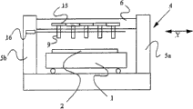
In Fig. 2, lithographic equipment is configured to along a direction, " x " scanning direction substrate 2 lip-deep X-Y schemes.This equipment comprises the substrate platen 1 that substrate 2 has been installed on it.Using drive unit (not shown in Figure 2) can make substrate platen 1 is the x direction along the direction of scanning, and y (and z) direction moves, and this drive unit is worked under the control of control system 3.
At substrate 2 and substrate platen 1 trolley frame (trolley frame) 4 has been installed, this framework is fixed with respect to substrate platen 1.As shown in Figure 3, framework 4 comprises supporting leg 5a, 5b and stand 6.Stand 6 is supported on supporting leg 5a and the 5b and strides across the space of substrate platen 1 top.Stand 6 supports one group of optical projection system 7 (11 this systems have been shown among Fig. 2), and each optical projection system is described in conjunction with Fig. 1 hereinbefore.During framework 4 inswept substrate 2, rear along the location by towards stand 6 of optical projection system 7, and optical projection system 7 is configured such that to be provided in conjunction with the figure pencil of forms that produces on the y direction the fully covering to substrate 2.
In one example, can control individually each optical projection system 7, thereby change the position of patterned light irradiation substrate 2, and change the shape of this beam.As previously mentioned, normally realize this point by phorogenesis in the digital figure of the independent controllable elements array 104 that forms graphical device.Produce the digital signal that is applied to optical projection system 7 by control system 3.
One group of alignment mark detector 9 is by the location, forward position towards stand 6.Should be appreciated that, although Fig. 2 and 3 has set forth 5 this detectors, this number can change.Each detector 9 is configured to survey alignment mark 10 in substrate 2 lip-deep positions.In addition, each detector 9 passes the visual field of detector 9 with respect to which alignment mark of position sensing 10 of trolley frame 4, thereby determines the position of optical projection system 7.
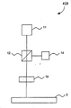
Fig. 4 has schematically set forth according to an embodiment of the invention alignment mark detector 409.Detector 409 is an example arrangement of detector 9.Each alignment mark detector 409 comprises radiation source 11, and this radiation source works in the wavelength that can not cause substrate 2 lip-deep photoresist exposures.For example, radiation source 11 can produce ruddiness, and this light is moved with respect to the light that optical projection system 7 employed exposing beams (for example 350 to 450nm) are provided.This radiation uses projection optics element 13 to be projected on the surface of substrate 2 by beam splitter 12.The light of radiation sensor 14 with probing substrate 2 surface reflections is provided.Usually, by photoresist on the substrate 2 be exposed and developing regional provides alignment mark 10 (not shown in Figure 4), this alignment mark causes occurring high-caliber reflection.Sensor 14 reflexes to the high level reflection and gets back to low-level variation and survey alignment mark 10 by seeking from low-level.Sensor 14 provides any deviation of output signal (namely this control system is configured to determine that the alignment mark 10 that detects is with respect to the position of trolley frame 4) and this position and desired location to control system 3.
Should be appreciated that, can use other detector configuration, be included in the detector configuration of sharing between the detector 9 such as the element of radiation source.
Refer again to Fig. 3, each alignment mark detector 9 is installed on the Linear Driving machinery device 15 in this example, and this drive mechanism comprises linear electric machine.It is mobile at stand 6 that drive mechanism 15 can drive detector 9 in the y-direction, and removable certain limit.Usually, this allows mobile half the distance in the interval of each detector 9 between each detector 9, so that the detector 9 of combination can provide in the y-direction the complete covering to substrate 2.
Each drive mechanism 15 is coupled to the control system 3 of the position of control detector 9.In this example, control system 3 is from one group of laser interferometer system, 16 pick-up probe positional informations.For each alignment mark detector 9, laser instrument and sensor device that interferometer system 16 comprises the catoptron that is fixed to detector 9 and is fixed to framework 4.When mobile detector 9, the output of control system 3 each sensors of monitoring is in order to calculate the position of number and definite detector 9 of interference fringe.For the consideration that gets across, only an interferometer system 16 has been shown in Fig. 2 and 3, certainly can understand and can be each detector 9 a this system is provided.
In another example, the positional information that control system 3 receives from operating personnel's input.
Example substrate
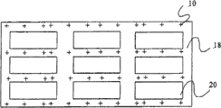
Fig. 5 and 6 has set forth respectively according to various embodiments of the present invention, has the substrate 17 of different panels layout and 18 vertical view.Substrate 17,18 has identical overall dimension, but is designed to hold different flat panel display size.The substrate 17 of Fig. 5 is designed to hold 4 measure-alike panels 19, and the substrate 18 of Fig. 6 is designed to hold 9 measure-alike panels 20.Alignment mark on each panel is aligned to and is suitable for this panel layout and maximizes the precision that substrate 17,18 is aligned between exposure period.
Exemplary operations
With reference to figure 2,3 and 5, when preparing exposure substrate 17 is loaded on the substrate platen 1.The precision that realizes this process is generally several millimeters.In one example, operating personnel are programmed into the characteristic of substrate 17 in the control system 3, for example the position of the line number of alignment mark 10 and these row (in the y-direction).In another example, operating personnel input the substrate type code, and wherein the alignment mark data of every kind of substrate type are programmed in the control system 3 in advance.In arbitrary example, this operation causes the alignment mark detector 9 of proper number to be activated, and is 3 in this case, and utilizes corresponding Linear Driving machinery device 15 with the appropriate location of these detector movings to each row alignment mark 10 top.In one example, the visual field of detector 9 is enough to the positioning error on the substrate 17 on the substrate platen 1 is adjusted within about several millimeters.Perhaps, can carry out specific scanning sequence with on the centralized positioning of each detector 9 is capable to corresponding alignment mark.
In this example, during position locator 9, use laser interferometer system 16 can accurately record its position.Final position information is fed into control system 3.Usually, control system 3 is used in the y-direction translation substrate platen of this information 1 before scanning, thereby exactly with optical projection system and substrate alignment.The visual field of detector 9 is enough to this slight translation of accommodating substrates 17.Begin subsequently exposure, in the x-direction at 4 times scanning of trolley frame substrate 17.When each detector 9 detects alignment mark 10 through out-of-date, positional information is fed into control system 3.The front is described, control system 3 is according to the alignment mark information data that receives, and the optical element by adjusting optical projection system, adjusts the digital figure that is applied to independent controllable elements array, adjusts the combination in any of substrate platen position or these adjustment and correctly aim at optical projection system 7 and substrate 17.
With reference to figure 2,3 and 6, the data of operating personnel's input are so that 4 detectors 9 on the stand 6 are energized and move to the tram.The configuration of panel 20 and number are conducive to use 4 row alignment marks 10 on the substrate 18, use this 4 row alignment mark usually can improve alignment accuracy in the exposure process.
Fig. 7 shows the according to an embodiment of the invention process flow diagram of method of operating 700.In step 702, substrate is placed on the substrate platen.In step 704, select the alignment mark detector of proper number and it is moved to position in the use.In step 706, carry out scan exposure.
Conclusion
Various embodiment of the present invention described above should be understood that, only are that the mode with example illustrates these embodiment, and these embodiment are not for restriction the present invention.To those skilled in the art, do not leaving the variation that to carry out under the spirit and scope of the present invention on various forms or the details.Therefore, range of the present invention and scope are not limited by any aforementioned exemplary embodiment, and should only be limited by appended claims and equivalents thereof.
Claims (3)
1. lithographic equipment comprises:
Framework;
The substrate platen of support substrates, this substrate is provided with alignment mark in its surface;
Drive unit, described drive unit is along first direction moving substrate platform; And
A plurality of alignment mark detectors, described a plurality of alignment mark detectors are coupled to this framework and can move along the second direction vertical with first direction;
A plurality of drive mechanisms, each drive mechanism respectively with a plurality of alignment mark detectors in one be associated, each drive mechanism moves corresponding alignment mark detector along second direction; And
Control system, described control system is according to the characteristic of the substrate that comprises the multirow alignment mark and the multirow alignment mark position along second direction, determine in a plurality of alignment mark detectors the right quantity of the alignment mark detector that will be activated, and will determine the alignment mark detector moving that the to be activated appropriate position on the second direction
Wherein, each of a plurality of drive mechanisms can drive the alignment mark detector that is associated in certain limit, so that the alignment mark detector of combination provides along the complete covering of second direction to substrate.
2. equipment according to claim 1 also comprises:
A plurality of position transducers, each position transducer respectively with a plurality of alignment mark detectors in one be associated, each position transducer determines that corresponding alignment mark detector is with respect to the position of this framework.
3. alignment methods that is used for having the lithographic equipment of a plurality of alignment mark detectors comprises step:
Substrate is provided, and described substrate has the multirow alignment mark in its surface, and each alignment mark is arranged along first direction;
According to the characteristic of the substrate that comprises the multirow alignment mark and the multirow alignment mark position along second direction, determine in a plurality of alignment mark detectors that the right quantity of the alignment mark detector that will be activated and they are perpendicular to the appropriate location on the second direction of first direction; And
To determine that by the drive mechanism of a plurality of correspondences the alignment mark detector moving that will be activated is determined the position on the second direction,
Wherein, each of a plurality of drive mechanisms can drive the alignment mark detector that is associated in certain limit, so that the alignment mark detector of combination provides along the complete covering of second direction to substrate.
Applications Claiming Priority (3)
| Application Number | Priority Date | Filing Date | Title |
|---|---|---|---|
| US10/975183 | 2004-10-28 | ||
| US10/975,183 US7388663B2 (en) | 2004-10-28 | 2004-10-28 | Optical position assessment apparatus and method |
| US10/975,183 | 2004-10-28 |
Related Parent Applications (1)
| Application Number | Title | Priority Date | Filing Date |
|---|---|---|---|
| CN2005101185152A Division CN1766740B (en) | 2004-10-28 | 2005-10-27 | Optical position assessment apparatus and method |
Publications (2)
| Publication Number | Publication Date |
|---|---|
| CN101852992A CN101852992A (en) | 2010-10-06 |
| CN101852992B true CN101852992B (en) | 2013-01-09 |
Family
ID=35636881
Family Applications (2)
| Application Number | Title | Priority Date | Filing Date |
|---|---|---|---|
| CN2005101185152A Active CN1766740B (en) | 2004-10-28 | 2005-10-27 | Optical position assessment apparatus and method |
| CN2010101134518A Active CN101852992B (en) | 2004-10-28 | 2005-10-27 | Apparatus and method for optical position assessment |
Family Applications Before (1)
| Application Number | Title | Priority Date | Filing Date |
|---|---|---|---|
| CN2005101185152A Active CN1766740B (en) | 2004-10-28 | 2005-10-27 | Optical position assessment apparatus and method |
Country Status (7)
| Country | Link |
|---|---|
| US (1) | US7388663B2 (en) |
| EP (1) | EP1653288B1 (en) |
| JP (4) | JP4310302B2 (en) |
| KR (1) | KR100806280B1 (en) |
| CN (2) | CN1766740B (en) |
| SG (3) | SG172672A1 (en) |
| TW (2) | TWI326015B (en) |
Families Citing this family (47)
| Publication number | Priority date | Publication date | Assignee | Title |
|---|---|---|---|---|
| US7388663B2 (en) * | 2004-10-28 | 2008-06-17 | Asml Netherlands B.V. | Optical position assessment apparatus and method |
| WO2006069340A2 (en) * | 2004-12-21 | 2006-06-29 | Carnegie Mellon University | Lithography and associated methods, devices, and systems |
| US7459247B2 (en) * | 2004-12-27 | 2008-12-02 | Asml Netherlands B.V. | Lithographic apparatus and device manufacturing method |
| JP4533777B2 (en) * | 2005-02-28 | 2010-09-01 | 富士フイルム株式会社 | Sheet body position detection method and apparatus, and drawing apparatus using the same |
| US8411271B2 (en) * | 2005-12-28 | 2013-04-02 | Nikon Corporation | Pattern forming method, pattern forming apparatus, and device manufacturing method |
| EP2963498B8 (en) | 2006-01-19 | 2017-07-26 | Nikon Corporation | Exposure apparatus, exposure method, and device manufacturing method |
| KR20130057496A (en) | 2006-02-21 | 2013-05-31 | 가부시키가이샤 니콘 | Pattern forming apparatus, mark detecting apparatus, exposure apparatus, pattern forming method, exposure method and device manufacturing method |
| EP3293577A1 (en) | 2006-02-21 | 2018-03-14 | Nikon Corporation | Exposure apparatus, exposure method and device manufacturing method |
| EP3279739A1 (en) * | 2006-02-21 | 2018-02-07 | Nikon Corporation | Exposure apparatus, exposure method, and device manufacturing method |
| US7525671B2 (en) * | 2006-04-11 | 2009-04-28 | Micronic Laser Systems Ab | Registration method and apparatus therefor |
| KR101669785B1 (en) | 2006-08-31 | 2016-10-27 | 가부시키가이샤 니콘 | Mobile body drive system and mobile body drive method, pattern formation apparatus and method, exposure apparatus and method, device manufacturing method, and decision method |
| EP3064999B1 (en) | 2006-08-31 | 2017-07-26 | Nikon Corporation | Exposure apparatus, exposure method, and device manufacturing method |
| EP3279738A1 (en) | 2006-08-31 | 2018-02-07 | Nikon Corporation | Movable body drive method and movable body drive system, pattern formation method and apparatus, exposure method and apparatus, and device manufacturing method |
| KR101511929B1 (en) | 2006-09-01 | 2015-04-13 | 가부시키가이샤 니콘 | Mobile object driving method, mobile object driving system, pattern forming method and apparatus, exposure method and apparatus, device manufacturing method and calibration method |
| KR101604564B1 (en) | 2006-09-01 | 2016-03-17 | 가부시키가이샤 니콘 | Mobile body driving method, mobile body driving system, pattern forming method and apparatus, exposure method and apparatus and device manufacturing method |
| DE102006059818B4 (en) * | 2006-12-11 | 2017-09-14 | Kleo Ag | exposure system |
| US20090042115A1 (en) * | 2007-04-10 | 2009-02-12 | Nikon Corporation | Exposure apparatus, exposure method, and electronic device manufacturing method |
| US20090042139A1 (en) * | 2007-04-10 | 2009-02-12 | Nikon Corporation | Exposure method and electronic device manufacturing method |
| US20080270970A1 (en) * | 2007-04-27 | 2008-10-30 | Nikon Corporation | Method for processing pattern data and method for manufacturing electronic device |
| WO2009150901A1 (en) * | 2008-06-09 | 2009-12-17 | シャープ株式会社 | Exposure apparatus and exposure method |
| US8432548B2 (en) * | 2008-11-04 | 2013-04-30 | Molecular Imprints, Inc. | Alignment for edge field nano-imprinting |
| JP5381029B2 (en) * | 2008-11-10 | 2014-01-08 | ウシオ電機株式会社 | Exposure equipment |
| DE102009032210B4 (en) * | 2009-07-03 | 2011-06-09 | Kleo Ag | processing plant |
| JP5351287B2 (en) * | 2010-01-21 | 2013-11-27 | シャープ株式会社 | Substrate, exposure method for substrate, photo-alignment processing method |
| NL2005975A (en) * | 2010-03-03 | 2011-09-06 | Asml Netherlands Bv | Imprint lithography. |
| RU2535999C2 (en) | 2010-07-12 | 2014-12-20 | Отис Элевэйтор Компани | Speed and position determination system |
| NL2007155A (en) | 2010-08-25 | 2012-02-28 | Asml Netherlands Bv | Stage apparatus, lithographic apparatus and method of positioning an object table. |
| EP2691811B1 (en) * | 2011-03-29 | 2018-01-31 | ASML Netherlands B.V. | Measurement of the position of a radiation beam spot in lithography |
| KR101326107B1 (en) * | 2011-12-20 | 2013-11-06 | 삼성디스플레이 주식회사 | Laser processing apparatus and control method thereof |
| CN102654387B (en) * | 2012-05-25 | 2014-07-02 | 南京理工大学 | Online industrial robot calibration device based on spatial curved surface restraint |
| CN102706277B (en) * | 2012-05-25 | 2014-11-05 | 南京理工大学 | Industrial robot online zero position calibration device based on all-dimensional point constraint and method |
| CN104102092A (en) * | 2013-04-11 | 2014-10-15 | 常熟晶悦半导体设备有限公司 | Four-phtotoheads optical exposure machine having automatic aligning system |
| JP5605770B2 (en) * | 2013-05-20 | 2014-10-15 | 株式会社ニコン | Display element manufacturing method and display element manufacturing apparatus |
| JP6228420B2 (en) * | 2013-10-08 | 2017-11-08 | キヤノン株式会社 | Detection apparatus, lithographic apparatus, and article manufacturing method |
| KR102419494B1 (en) * | 2014-09-29 | 2022-07-12 | 삼성디스플레이 주식회사 | Maskless exposure device, maskless exposure method and display substrate manufactured by the maskless exposure device and maskless exposure method |
| KR102255033B1 (en) * | 2015-01-13 | 2021-05-25 | 삼성디스플레이 주식회사 | Maskless exposure device and maskless exposure method using the same |
| TWI753865B (en) * | 2015-11-03 | 2022-02-01 | 以色列商奧寶科技有限公司 | Stitchless direct imaging for high resolution electronic patterning |
| US10707107B2 (en) | 2015-12-16 | 2020-07-07 | Kla-Tencor Corporation | Adaptive alignment methods and systems |
| CN109791368B (en) * | 2016-09-27 | 2021-11-26 | 株式会社尼康 | Determining method and device, program, information recording medium, exposure device, layout information providing method, layout method, mark detecting method, exposure method, and device manufacturing method |
| CN108121162B (en) * | 2016-11-29 | 2019-09-17 | 上海微电子装备(集团)股份有限公司 | A kind of projection aligner and exposure method |
| EP3339959A1 (en) * | 2016-12-23 | 2018-06-27 | ASML Netherlands B.V. | Method of determining a position of a feature |
| JP6447845B2 (en) * | 2017-04-18 | 2019-01-09 | 株式会社ニコン | Exposure apparatus, flat panel display manufacturing method, device manufacturing method, and exposure method |
| US11152238B2 (en) * | 2017-11-30 | 2021-10-19 | Taiwan Semiconductor Manufacturing Co., Ltd. | Semiconductor processing stage profiler jig |
| JP7045890B2 (en) * | 2018-03-20 | 2022-04-01 | 株式会社Screenホールディングス | Pattern drawing device and pattern drawing method |
| CN110296666B (en) * | 2018-03-23 | 2021-04-20 | 泓邦科技有限公司 | Three-dimensional measuring device |
| JP2019045875A (en) * | 2018-12-07 | 2019-03-22 | 株式会社ニコン | Exposure device, manufacturing method of flat panel display, device manufacturing method and exposure method |
| CN112445088A (en) * | 2020-12-04 | 2021-03-05 | 百及纳米科技(上海)有限公司 | Stepping photoetching machine, working method thereof and graph alignment device |
Citations (5)
| Publication number | Priority date | Publication date | Assignee | Title |
|---|---|---|---|---|
| US5220176A (en) * | 1991-09-13 | 1993-06-15 | Nikon Corporation | Apparatus and method for detecting alignment marks having alignment optical systems' driving means |
| EP0715214A1 (en) * | 1994-11-29 | 1996-06-05 | Ushiodenki Kabushiki Kaisha | Process for positioning a mask relative to a workpiece and device for carrying out the process |
| EP0786702A2 (en) * | 1996-01-11 | 1997-07-30 | Ushiodenki Kabushiki Kaisha | Process for pattern searching and a device for positioning of a mask to a workpiece |
| CN1333554A (en) * | 2001-07-26 | 2002-01-30 | 清华大学 | Alignment method and apparatus for array type optical probe scanning IC photoetching system |
| CN1459671A (en) * | 2002-05-22 | 2003-12-03 | 尼康株式会社 | Exposure method, exposure apparatus and element mfg. method |
Family Cites Families (46)
| Publication number | Priority date | Publication date | Assignee | Title |
|---|---|---|---|---|
| JPH079877B2 (en) * | 1986-07-11 | 1995-02-01 | 株式会社ニコン | Alignment device |
| US5523193A (en) * | 1988-05-31 | 1996-06-04 | Texas Instruments Incorporated | Method and apparatus for patterning and imaging member |
| GB8827952D0 (en) * | 1988-11-30 | 1989-01-05 | Screen Form Inc | Display device |
| JPH02242259A (en) * | 1989-03-15 | 1990-09-26 | Toppan Printing Co Ltd | Method and device for registration in substrate exposing |
| US5296891A (en) * | 1990-05-02 | 1994-03-22 | Fraunhofer-Gesellschaft Zur Forderung Der Angewandten Forschung E.V. | Illumination device |
| JP3031993B2 (en) * | 1990-11-05 | 2000-04-10 | 株式会社東芝 | X-ray exposure equipment |
| US5229872A (en) * | 1992-01-21 | 1993-07-20 | Hughes Aircraft Company | Exposure device including an electrically aligned electronic mask for micropatterning |
| US6219015B1 (en) | 1992-04-28 | 2001-04-17 | The Board Of Directors Of The Leland Stanford, Junior University | Method and apparatus for using an array of grating light valves to produce multicolor optical images |
| JP3224041B2 (en) | 1992-07-29 | 2001-10-29 | 株式会社ニコン | Exposure method and apparatus |
| US5496407A (en) * | 1993-04-19 | 1996-03-05 | Mcaleavey; Michael E. | System and method for monitoring and controlling thickness |
| US5729331A (en) | 1993-06-30 | 1998-03-17 | Nikon Corporation | Exposure apparatus, optical projection apparatus and a method for adjusting the optical projection apparatus |
| US5614988A (en) * | 1993-12-06 | 1997-03-25 | Nikon Corporation | Projection exposure apparatus and method with a plurality of projection optical units |
| JP3339149B2 (en) | 1993-12-08 | 2002-10-28 | 株式会社ニコン | Scanning exposure apparatus and exposure method |
| KR100377887B1 (en) * | 1994-02-10 | 2003-06-18 | 가부시키가이샤 니콘 | Sort method |
| US5492601A (en) * | 1994-07-29 | 1996-02-20 | Wangner Systems Corporation | Laser apparatus and method for monitoring the de-watering of stock on papermaking machines |
| US5617211A (en) * | 1994-08-16 | 1997-04-01 | Nikon Corporation | Exposure apparatus |
| US5546808A (en) * | 1994-09-06 | 1996-08-20 | Harris Instrument Corporation | Apparatus and method for binocular measurement system |
| JP3050498B2 (en) * | 1994-10-17 | 2000-06-12 | 日立電子エンジニアリング株式会社 | Adjustment method of position shift amount measuring optical system and position shift amount measurement apparatus |
| KR100399813B1 (en) * | 1994-12-14 | 2004-06-09 | 가부시키가이샤 니콘 | Exposure apparatus |
| US5677703A (en) | 1995-01-06 | 1997-10-14 | Texas Instruments Incorporated | Data loading circuit for digital micro-mirror device |
| US5530482A (en) | 1995-03-21 | 1996-06-25 | Texas Instruments Incorporated | Pixel data processing for spatial light modulator having staggered pixels |
| JP2994232B2 (en) | 1995-07-28 | 1999-12-27 | ウシオ電機株式会社 | Mask-to-mask or mask-to-work alignment method and apparatus |
| DE69729659T2 (en) | 1996-02-28 | 2005-06-23 | Johnson, Kenneth C., Santa Clara | MIKROLINSEN RASTER DEVICE FOR MICROLITHOGRAPHY AND FOR CONFOCUS MICROSCOPY WITH LARGE RECORDING FIELD |
| EP0956516B1 (en) | 1997-01-29 | 2002-04-10 | Micronic Laser Systems Ab | Method and apparatus for the production of a structure by focused laser radiation on a photosensitively coated substrate |
| US6177980B1 (en) | 1997-02-20 | 2001-01-23 | Kenneth C. Johnson | High-throughput, maskless lithography system |
| SE509062C2 (en) | 1997-02-28 | 1998-11-30 | Micronic Laser Systems Ab | Data conversion method for a multi-beam laser printer for very complex microcolytographic designs |
| US5982553A (en) | 1997-03-20 | 1999-11-09 | Silicon Light Machines | Display device incorporating one-dimensional grating light-valve array |
| JP4029130B2 (en) * | 1997-06-03 | 2008-01-09 | 株式会社ニコン | Exposure apparatus and exposure method |
| US5956134A (en) * | 1997-07-11 | 1999-09-21 | Semiconductor Technologies & Instruments, Inc. | Inspection system and method for leads of semiconductor devices |
| EP1028456A4 (en) * | 1997-09-19 | 2003-03-05 | Nikon Corp | Stage device, a scanning aligner and a scanning exposure method, and a device manufactured thereby |
| SE9800665D0 (en) | 1998-03-02 | 1998-03-02 | Micronic Laser Systems Ab | Improved method for projection printing using a micromirror SLM |
| US6261728B1 (en) * | 1998-10-19 | 2001-07-17 | Vanguard International Semiconductor Corporation | Mask image scanning exposure method |
| JP2001033976A (en) * | 1999-07-21 | 2001-02-09 | Nikon Corp | Alignment device, alignment method and exposure device |
| JP2001118773A (en) * | 1999-10-18 | 2001-04-27 | Nikon Corp | Stage device and exposure system |
| US6355994B1 (en) * | 1999-11-05 | 2002-03-12 | Multibeam Systems, Inc. | Precision stage |
| KR100827874B1 (en) * | 2000-05-22 | 2008-05-07 | 가부시키가이샤 니콘 | Exposure apparatus, method for manufacturing thereof, method for exposing, method for manufacturing microdevice, and method for manufacturing device |
| JP3563384B2 (en) * | 2001-11-08 | 2004-09-08 | 大日本スクリーン製造株式会社 | Image recording device |
| JP2004012903A (en) * | 2002-06-07 | 2004-01-15 | Fuji Photo Film Co Ltd | Aligner |
| SG130007A1 (en) * | 2002-06-12 | 2007-03-20 | Asml Netherlands Bv | Lithographic apparatus and device manufacturing method |
| US6870554B2 (en) * | 2003-01-07 | 2005-03-22 | Anvik Corporation | Maskless lithography with multiplexed spatial light modulators |
| SE0300453D0 (en) * | 2003-02-20 | 2003-02-20 | Micronic Laser Systems Ab | Pattern generation method |
| JP2004272167A (en) * | 2003-03-12 | 2004-09-30 | Dainippon Printing Co Ltd | Pattern forming apparatus, method for forming pattern, and base material |
| US6950188B2 (en) * | 2003-04-23 | 2005-09-27 | International Business Machines Corporation | Wafer alignment system using parallel imaging detection |
| EP1482373A1 (en) * | 2003-05-30 | 2004-12-01 | ASML Netherlands B.V. | Lithographic apparatus and device manufacturing method |
| JP3860582B2 (en) * | 2003-07-31 | 2006-12-20 | 株式会社東芝 | Manufacturing method of semiconductor device |
| US7388663B2 (en) * | 2004-10-28 | 2008-06-17 | Asml Netherlands B.V. | Optical position assessment apparatus and method |
-
2004
- 2004-10-28 US US10/975,183 patent/US7388663B2/en active Active
-
2005
- 2005-09-20 EP EP05255793.1A patent/EP1653288B1/en active Active
- 2005-09-28 SG SG2011040466A patent/SG172672A1/en unknown
- 2005-09-28 SG SG200506271A patent/SG121953A1/en unknown
- 2005-09-28 SG SG200807524-4A patent/SG147421A1/en unknown
- 2005-10-17 TW TW094136097A patent/TWI326015B/en active
- 2005-10-17 TW TW098102116A patent/TW200921304A/en unknown
- 2005-10-27 JP JP2005312849A patent/JP4310302B2/en active Active
- 2005-10-27 CN CN2005101185152A patent/CN1766740B/en active Active
- 2005-10-27 CN CN2010101134518A patent/CN101852992B/en active Active
- 2005-10-28 KR KR1020050102372A patent/KR100806280B1/en active IP Right Grant
-
2008
- 2008-09-16 JP JP2008236347A patent/JP4648442B2/en active Active
-
2010
- 2010-08-19 JP JP2010183894A patent/JP5238771B2/en active Active
-
2012
- 2012-11-20 JP JP2012253918A patent/JP5554819B2/en active Active
Patent Citations (5)
| Publication number | Priority date | Publication date | Assignee | Title |
|---|---|---|---|---|
| US5220176A (en) * | 1991-09-13 | 1993-06-15 | Nikon Corporation | Apparatus and method for detecting alignment marks having alignment optical systems' driving means |
| EP0715214A1 (en) * | 1994-11-29 | 1996-06-05 | Ushiodenki Kabushiki Kaisha | Process for positioning a mask relative to a workpiece and device for carrying out the process |
| EP0786702A2 (en) * | 1996-01-11 | 1997-07-30 | Ushiodenki Kabushiki Kaisha | Process for pattern searching and a device for positioning of a mask to a workpiece |
| CN1333554A (en) * | 2001-07-26 | 2002-01-30 | 清华大学 | Alignment method and apparatus for array type optical probe scanning IC photoetching system |
| CN1459671A (en) * | 2002-05-22 | 2003-12-03 | 尼康株式会社 | Exposure method, exposure apparatus and element mfg. method |
Also Published As
| Publication number | Publication date |
|---|---|
| SG121953A1 (en) | 2006-05-26 |
| TWI326015B (en) | 2010-06-11 |
| JP2010268005A (en) | 2010-11-25 |
| CN1766740B (en) | 2010-05-05 |
| CN101852992A (en) | 2010-10-06 |
| EP1653288A1 (en) | 2006-05-03 |
| SG172672A1 (en) | 2011-07-28 |
| JP5238771B2 (en) | 2013-07-17 |
| EP1653288B1 (en) | 2019-05-15 |
| US20060092419A1 (en) | 2006-05-04 |
| TW200921304A (en) | 2009-05-16 |
| JP4648442B2 (en) | 2011-03-09 |
| JP2006128693A (en) | 2006-05-18 |
| SG147421A1 (en) | 2008-11-28 |
| JP2009010420A (en) | 2009-01-15 |
| JP4310302B2 (en) | 2009-08-05 |
| JP5554819B2 (en) | 2014-07-23 |
| JP2013047850A (en) | 2013-03-07 |
| TW200627096A (en) | 2006-08-01 |
| US7388663B2 (en) | 2008-06-17 |
| KR20060052321A (en) | 2006-05-19 |
| CN1766740A (en) | 2006-05-03 |
| KR100806280B1 (en) | 2008-02-22 |
Similar Documents
| Publication | Publication Date | Title |
|---|---|---|
| CN101852992B (en) | Apparatus and method for optical position assessment | |
| CN1684002B (en) | Flat plate printing apparatus and device manufacturing method | |
| KR100767090B1 (en) | Lithographic Apparatus and Device Manufacturing Method | |
| US8502954B2 (en) | Lithographic apparatus and device manufacturing method | |
| US7477403B2 (en) | Optical position assessment apparatus and method | |
| JP2010068002A (en) | Lithographic device and method of manufacturing device | |
| US7239393B2 (en) | Calibration method for a lithographic apparatus and device manufacturing method | |
| CN101105641A (en) | Correction of off-axis translation of optical elements in an optical zoom assembly |
Legal Events
| Date | Code | Title | Description |
|---|---|---|---|
| C06 | Publication | ||
| PB01 | Publication | ||
| C10 | Entry into substantive examination | ||
| SE01 | Entry into force of request for substantive examination | ||
| C14 | Grant of patent or utility model | ||
| GR01 | Patent grant |