CN101841663B - Combinational circuit of image sensor and method - Google Patents
Combinational circuit of image sensor and method Download PDFInfo
- Publication number
- CN101841663B CN101841663B CN2009101287953A CN200910128795A CN101841663B CN 101841663 B CN101841663 B CN 101841663B CN 2009101287953 A CN2009101287953 A CN 2009101287953A CN 200910128795 A CN200910128795 A CN 200910128795A CN 101841663 B CN101841663 B CN 101841663B
- Authority
- CN
- China
- Prior art keywords
- signal
- imageing sensor
- picture signal
- group
- sampling
- Prior art date
- Legal status (The legal status is an assumption and is not a legal conclusion. Google has not performed a legal analysis and makes no representation as to the accuracy of the status listed.)
- Expired - Fee Related
Links
- 238000000034 method Methods 0.000 title claims abstract description 16
- 238000005070 sampling Methods 0.000 claims abstract description 9
- 230000002596 correlated effect Effects 0.000 claims abstract description 5
- 150000001875 compounds Chemical class 0.000 claims description 10
- 239000003990 capacitor Substances 0.000 abstract description 16
- 230000005540 biological transmission Effects 0.000 description 7
- 230000003287 optical effect Effects 0.000 description 6
- 230000003321 amplification Effects 0.000 description 3
- 239000002131 composite material Substances 0.000 description 3
- 238000003199 nucleic acid amplification method Methods 0.000 description 3
- 239000004065 semiconductor Substances 0.000 description 3
- 101100400452 Caenorhabditis elegans map-2 gene Proteins 0.000 description 2
- 230000001427 coherent effect Effects 0.000 description 2
- 230000000295 complement effect Effects 0.000 description 2
- 230000001808 coupling effect Effects 0.000 description 2
- 230000002045 lasting effect Effects 0.000 description 2
- 229910044991 metal oxide Inorganic materials 0.000 description 2
- 150000004706 metal oxides Chemical class 0.000 description 2
- 230000007704 transition Effects 0.000 description 2
- 230000008878 coupling Effects 0.000 description 1
- 238000010168 coupling process Methods 0.000 description 1
- 238000005859 coupling reaction Methods 0.000 description 1
- 230000003467 diminishing effect Effects 0.000 description 1
- 238000005516 engineering process Methods 0.000 description 1
- 239000012467 final product Substances 0.000 description 1
Images


Landscapes
- Transforming Light Signals Into Electric Signals (AREA)
- Solid State Image Pick-Up Elements (AREA)
Abstract
The invention relates to a combinational circuit of an image sensor and a method. Firstly, a column amplifier (CA) is reset, so that a CA reset signal is generated. A capacitor and a switcher are coupled between the output of the image sensor and the input of the column amplifier. A correlated double sampling (CDS) circuit is controlled to receive the output of the column amplifier. The switcher is controlled so that the first group of image signals of the image sensor are transmitted and stored in the CDS circuit, and moreover, the second group of image signals are added on the stored first group of image signals.
Description
Technical field
The present invention relates to imageing sensor, combination (binning) circuit and the method for particularly a kind of compound vertical pixel shared (multiple-vertical-pixels-sharing) imageing sensor.
Background technology
Semiconductor image sensor (for example Charged Coupled Device (CCD) or complementary metal oxide semiconductors (CMOS) (CMOS) transducer) generally is used in camera or the video camera; The image transitions that is used for visible light is an electronic signal, is convenient to follow-up storage, transmission or demonstration.
The partial pixel of imageing sensor (or optical diode) can a shared circuit, to reduce the size of integrated circuit.Shared framework can adopt vertical mode (that is, be positioned at the shared circuit of the pixel of delegation), also can adopt horizontal mode (that is, be positioned at the shared circuit of pixel of same row).Fig. 1 shows conventional composite vertical pixel common image sensor 10, and it has the pixel common circuit that many groups (that is, A group, B group etc.) adopt vertical shared mode.
When making more and more many pixels (or optical diode) in the imageing sensor, the area of each pixel and image intensity thereof can relative diminishing.In order to strengthen image intensity, need the signal of a plurality of pixels be given addition (or being called combination of pixels) usually to obtain better signal noise ratio (SNR).
Yet, for the vertical shared imageing sensor of aforementioned conventional,, will meet with difficulty if will cross over different groups to carry out combination of pixels, solve only if increase some extra circuit.For example, in Fig. 1, if will in the A group, carry out combination of pixels, as long as (tx_A_n, n=1 2...) open and get final product associated transport door (transfergate) simultaneously that will organize.Yet, if with open A group and B group transmission gate (tx_A_n, tx_B_n, n=1, (column) node (col) of 2...), being expert at is located to cause the conflict between the signal.Therefore, for conventional composite vertical pixel common image sensor 10, its combination of pixels number can receive very big restriction.
In view of conventional image sensor; Compound vertical pixel common image sensor 10 for example shown in Figure 1; Can't carry out the combination of signal effectively; Therefore need badly and propose a kind of novel combination circuit and method, be used to cross over different groups to carry out the combination of signal applicable to imageing sensor (particularly compound vertical pixel common image sensor).
Summary of the invention
In view of above-mentioned, one of the object of the invention is to propose a kind of combinational circuit and method applicable to imageing sensor (particularly compound vertical pixel common image sensor), is used to cross over different groups effectively to carry out the combination of signal.
According to the features of this invention, at first, the row amplifier (CA) of resetting, thereby produce the CA reset signal.Coupling capacitance and switching device shifter are between the input of the output of imageing sensor and row amplifier.Control correlated-double-sampling (CDS) circuit is to receive the output of capable amplifier.Wherein, control switch device makes the picture signal of Band 1 of imageing sensor be transmitted and is stored in the CDS circuit, and the picture signal of second group then is added on the picture signal of the Band 1 of being stored.
Another feature according to the present invention, at first, replacement delegation amplifier (CA) is used to produce the CA reset signal.Receive the reset signal of Band 1, then use the picture signal of row amplifier with the amplification Band 1, and the picture signal of storage Band 1.Next, receive the reset signal of second group, then use the row amplifier amplifying the picture signal of second group, and it is added on the picture signal of the Band 1 of being stored.
Description of drawings
Fig. 1 shows conventional composite vertical pixel common image sensor;
Fig. 2 shows the combinational circuit of the embodiment of the invention, and it is applicable to compound vertical pixel common image sensor;
Fig. 3 A to Fig. 3 D shows the equivalent electric circuit of the embodiment of the invention each step when carrying out combination operation;
The coherent signal sequential chart of Fig. 4 displayed map 2, Fig. 3 A to Fig. 3 D.Fig. 5 shows the flow chart of embodiment of the invention combination operation.
Embodiment
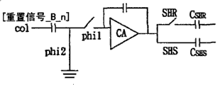
Fig. 2 shows the combinational circuit 20 of the embodiment of the invention, and it is applicable to compound vertical pixel common image sensor 22.This compound vertical pixel common image sensor 22 comprises a plurality of groups, and for example A group (22A), B group (22B), each group are then according to the indivedual shared interlock circuits of vertical shared mode.Imageing sensor 22 can be (but not being defined as) Charged Coupled Device (CCD) or complementary metal oxide semiconductors (CMOS) (CMOS) transducer, and the image transitions that is used for visible light is an electronic signal.The output of combinational circuit 20 can be fed to amplifier (not being shown in the accompanying drawing), for example programmable gain amplifier (programmable gain amplifier, PGA).Above-mentioned imageing sensor 22 and combinational circuit 20 can be applicable in the digital image processing apparatus, for example (but not being defined as) camera or video camera.
With the A group is example, and each group of imageing sensor 22 comprises reset transistor rst_A, source follower sf_A, selects transistor sel_A and a plurality of transmission transistor (or transmission gate) (tx_A_1, tx_A_2 etc.).For for simplicity, transistor in the accompanying drawing (or switch) and control signal thereof are then used identical symbol.In accompanying drawing, when reset transistor rst_A is unlocked, can be used for optical diode (D_A_1, D_A_2 etc.) is reset to a replacement reference voltage.When source follower sf_A is unlocked, can be used for cushioning the picture signal of optical diode (D_A_1, D_A_2 etc.).When selecting transistor sel_A to be opened, then allow reading of pixel image signal by character line (word line).When transmission transistor (tx_A_1, tx_A_2 etc.) when being unlocked, can be used for transmitting respectively the pixel image signal of optical diode (D_A_1, D_A_2 etc.).Reset transistor rst_A, source follower sf_A and selection transistor sel_A are common to optical diode (D_A_1, D_A_2 etc.).The output of each group (A, B etc.) then is electrically coupled with capable node (col) jointly.
Fig. 3 A to Fig. 3 D shows the equivalent electric circuit of the embodiment of the invention each step when carrying out combination operation.The coherent signal sequential chart of Fig. 4 displayed map 2, Fig. 3 A to Fig. 3 D.Fig. 5 then shows the flow chart of embodiment of the invention combination operation.Though it is example that present embodiment carries out combination operation with A group and B group, yet the present invention is also applicable to the combination operation of other group.
When carrying out combination operation, at first, closed CA reset switch CA_rst (100) is used for row amplifier CA is reset (step 50), shown in Fig. 3 A.The SHR switch is closed (101), makes the CA reset signal be stored in SHR capacitor C SHR.In this stage, the SHS switch also is closed (102).In the practice, active SHR signal and active SHS signal have one section overlapping, and it is in order to prevent coupling effect (coupling effect).In another embodiment, the SHS switch in this stage is what break off.In this simultaneously, (A group) reset transistor rst_A is unlocked (103), and selects transistor sel_A also be unlocked (104).Then, through closed second switch phi2 (105) (but breaking off the first switch phi1), make the output reset signal of A group be received and be stored in capacitor C (step 50).
Next, shown in Fig. 3 B, the transmission transistor tx_A_n of A group (n=1,2...) be unlocked (106), and the first switch phi1 is closed (107), but second switch phi2 (108) then for breaking off.Thus; The input voltage of row amplifier CA is equivalent to (A group) picture signal and deducts (A group) reset signal of being stored; This input voltage then receives the amplification (step 51) of capable amplifier CA, the lasting closure of the SHS switch of this moment, but break off SHR switch (109).Thus, the picture signal of A group thereby be stored in the SHS capacitor C SHS.
Then, shown in Fig. 3 C, (B group) reset transistor rst_B is unlocked (110), and selects transistor sel_B also be unlocked (111).Then, through closed second switch phi2 (112) (but breaking off the first switch phi1), make the output reset signal of B group be received and be stored in capacitor C (step 52).
Next, shown in Fig. 3 D, the transmission transistor tx_B_n of B group (n=1,2...) be unlocked (113), and the first switch phi1 is closed (114), but second switch phi2 (115) then for breaking off.Thus, the input voltage of row amplifier CA is equivalent to (B group) picture signal and deducts (B group) reset signal of being stored, and this input voltage then receives the amplification of capable amplifier CA, the lasting closure of the SHS switch of this moment, but break off the SHR switch.Because it is closed that the SHS switch continues, thereby (or combination) to previous (A combination) voltage that is stored in SHS capacitor C SHS (step 53) that make the picture signal of B group be able to add, thereby the operation of completion signal combination.
According to the embodiment of the invention, in compound vertical pixel common image sensor, can cross over different groups (for example A group in the accompanying drawing and B group) and carry out the combination of signal effectively, can not produce the conflict between the signal.
The above is merely the preferred embodiments of the present invention, is not to be used to limit claim scope of the present invention; All other do not break away from the equivalence of being accomplished under the spirit that invention discloses and changes or modify, and all should be included in the following claim scope.
Claims (16)
1. the combinational circuit of an imageing sensor comprises:
The row amplifier then produces capable amplifier reset signal when it is reset;
Electric capacity and switching device shifter are coupled between the input of output and said capable amplifier of said imageing sensor; And
Correlated double sampling circuit is controlled to receive the output of said capable amplifier;
Wherein, control said switching device shifter and make the picture signal of Band 1 of said imageing sensor be transmitted and be stored in the said correlated double sampling circuit, and the picture signal of second group then is added on the picture signal of the said Band 1 of being stored.
2. the combinational circuit of imageing sensor as claimed in claim 1, wherein above-mentioned imageing sensor is compound vertical pixel common image sensor.
3. the combinational circuit of imageing sensor as claimed in claim 1 also comprises feedback capacity, is coupled between the output and input of said capable amplifier.
4. the combinational circuit of imageing sensor as claimed in claim 3 also comprises capable amplifier reset switch, is coupled between the output and input of said capable amplifier.
5. the combinational circuit of imageing sensor as claimed in claim 1, wherein first pole plate of above-mentioned electric capacity is coupled to the output of said imageing sensor, and said switching device shifter comprises:
First switch is coupled between second pole plate of input and said electric capacity of said capable amplifier; And
Second switch is coupled between second pole plate and ground of said electric capacity.
6. the combinational circuit of imageing sensor as claimed in claim 4, wherein above-mentioned correlated double sampling circuit comprises:
Sampling-maintenance-reset signal switch, said capable amplifier reset signal is used to sample;
Sampling-maintenance-reset signal electric capacity is coupled to said sampling-maintenance-reset signal switch, is used to keep said capable amplifier reset signal;
Sampling-maintenance-picture signal switch, the picture signal of the said imageing sensor that is used to sample; And
Sampling-maintenance-picture signal electric capacity is coupled to said sampling-maintenance-picture signal switch, is used to keep said picture signal.
7. signal combination methods that is applicable to imageing sensor comprises:
(a) replacement row amplifier is used to produce capable amplifier reset signal;
(b) reset signal of reception Band 1;
(c) use said capable amplifier amplifying the picture signal of said Band 1, and then store the picture signal of said Band 1;
(d) reset signal of reception second group; And
(e) use said capable amplifier amplifying the picture signal of said second group, and then it is added on the picture signal of the said Band 1 of being stored.
8. the signal combination methods that is applicable to imageing sensor as claimed in claim 7, wherein above-mentioned imageing sensor are compound vertical pixel common image sensor.
9. the signal combination methods that is applicable to imageing sensor as claimed in claim 7, wherein above-mentioned steps (a) and step (b) are carried out simultaneously.
10. the signal combination methods that is applicable to imageing sensor as claimed in claim 7, wherein above-mentioned capable amplifier reset signal is sampled and is stored in sampling-maintenance-reset signal electric capacity.
11. the signal combination methods that is applicable to imageing sensor as claimed in claim 7, the reset signal of the Band 1 that is wherein received in the above-mentioned steps (b) is stored in the electric capacity.
12. the signal combination methods that is applicable to imageing sensor as claimed in claim 11 is being carried out above-mentioned steps (c) before, and the reset signal of above-mentioned Band 1 is deducted from the picture signal of said Band 1.
13. the signal combination methods that is applicable to imageing sensor as claimed in claim 7, wherein the enlarged image signal of above-mentioned Band 1 is sampled and is stored in sampling-maintenance-picture signal electric capacity.
14. the signal combination methods that is applicable to imageing sensor as claimed in claim 7, the reset signal of second group that is wherein received in the above-mentioned steps (d) is stored in the electric capacity.
15. the signal combination methods that is applicable to imageing sensor as claimed in claim 14 is being carried out above-mentioned steps (e) before, the reset signal of above-mentioned second group deducts from the picture signal of said second group.
16. the signal combination methods that is applicable to imageing sensor as claimed in claim 7, the enlarged image signal of wherein above-mentioned second group are sampled and are stored in sampling-maintenance-picture signal electric capacity.
Priority Applications (1)
| Application Number | Priority Date | Filing Date | Title |
|---|---|---|---|
| CN2009101287953A CN101841663B (en) | 2009-03-19 | 2009-03-19 | Combinational circuit of image sensor and method |
Applications Claiming Priority (1)
| Application Number | Priority Date | Filing Date | Title |
|---|---|---|---|
| CN2009101287953A CN101841663B (en) | 2009-03-19 | 2009-03-19 | Combinational circuit of image sensor and method |
Publications (2)
| Publication Number | Publication Date |
|---|---|
| CN101841663A CN101841663A (en) | 2010-09-22 |
| CN101841663B true CN101841663B (en) | 2012-07-04 |
Family
ID=42744747
Family Applications (1)
| Application Number | Title | Priority Date | Filing Date |
|---|---|---|---|
| CN2009101287953A Expired - Fee Related CN101841663B (en) | 2009-03-19 | 2009-03-19 | Combinational circuit of image sensor and method |
Country Status (1)
| Country | Link |
|---|---|
| CN (1) | CN101841663B (en) |
Citations (3)
| Publication number | Priority date | Publication date | Assignee | Title |
|---|---|---|---|---|
| EP1085522A1 (en) * | 1999-09-15 | 2001-03-21 | Omnivision Technologies Inc. | Analog delay line for image processing |
| CN1307366A (en) * | 2000-01-29 | 2001-08-08 | 全视技术有限公司 | Monolithic colour metal-oxide-semiconductor imaging sensor and adjacent line readout method |
| CN101064787A (en) * | 2006-04-29 | 2007-10-31 | 格科微电子(上海)有限公司 | CMOS image sensor pixel |
-
2009
- 2009-03-19 CN CN2009101287953A patent/CN101841663B/en not_active Expired - Fee Related
Patent Citations (3)
| Publication number | Priority date | Publication date | Assignee | Title |
|---|---|---|---|---|
| EP1085522A1 (en) * | 1999-09-15 | 2001-03-21 | Omnivision Technologies Inc. | Analog delay line for image processing |
| CN1307366A (en) * | 2000-01-29 | 2001-08-08 | 全视技术有限公司 | Monolithic colour metal-oxide-semiconductor imaging sensor and adjacent line readout method |
| CN101064787A (en) * | 2006-04-29 | 2007-10-31 | 格科微电子(上海)有限公司 | CMOS image sensor pixel |
Also Published As
| Publication number | Publication date |
|---|---|
| CN101841663A (en) | 2010-09-22 |
Similar Documents
| Publication | Publication Date | Title |
|---|---|---|
| US9232161B2 (en) | Unit pixels configured to output different pixel signals through different lines and image sensors including the same | |
| US7256382B2 (en) | Solid state imaging device, method of driving solid state imaging device and image pickup apparatus | |
| KR102277597B1 (en) | Imaging device and electronic device | |
| US20130256510A1 (en) | Imaging device with floating diffusion switch | |
| KR102146231B1 (en) | Solid-state imaging element, and imaging device | |
| WO2011096207A1 (en) | Solid-state image capture device | |
| US8604407B2 (en) | Dual conversion gain pixel methods, systems, and apparatus | |
| US9979918B2 (en) | Image sensor and data tranmission method thereof | |
| US20160037101A1 (en) | Apparatus and Method for Capturing Images | |
| KR20160058489A (en) | Image sensor and method of outputting data in the image sensor | |
| CN110741629A (en) | Pixel unit and image sensor | |
| US20140204258A1 (en) | Image sensor, method for operating thereof, and image pick-up device having the same | |
| US7646410B2 (en) | Solid state image sensing device and method for subsampling using inter-column analog domain signal summation | |
| TWI856734B (en) | Solid-state imaging device, driving method for solid-state imaging device, and electronic equipment | |
| CN106982336B (en) | Implement the shared method of dynamic earth fault and imaging sensor in the imaging sensor with pipeline architecture | |
| US11758304B2 (en) | Image sensor | |
| CN101841633B (en) | Reading circuit of image sensor | |
| US20060044440A1 (en) | CMOS image sensor | |
| CN102164251B (en) | Signal processing circuit and signal processing method for image sensor | |
| JP2015095874A (en) | Solid state imaging device, imaging system, and method of driving solid state imaging device | |
| CN113676652B (en) | Image sensor, control method, control device, electronic apparatus, and storage medium | |
| KR102037283B1 (en) | Image sensor, image signal processor and electronic device including the same | |
| CN103053155B (en) | Filming apparatus | |
| CN101841663B (en) | Combinational circuit of image sensor and method | |
| CN116095519B (en) | Image sensors, sensor architectures, camera modules and electronic devices |
Legal Events
| Date | Code | Title | Description |
|---|---|---|---|
| C06 | Publication | ||
| PB01 | Publication | ||
| C10 | Entry into substantive examination | ||
| SE01 | Entry into force of request for substantive examination | ||
| C14 | Grant of patent or utility model | ||
| GR01 | Patent grant | ||
| CF01 | Termination of patent right due to non-payment of annual fee |
Granted publication date: 20120704 |
|
| CF01 | Termination of patent right due to non-payment of annual fee |