Summary of the invention
The present invention finishes at least a portion that solves above-mentioned problem, can be used as following mode or application examples and realizes.
[ application examples 1 ] should use-case the vibrating reed base portion that has the shaker arm more than 3 and connect described shaker arm, described shaker arm vibrates at thickness direction, and adjacent described shaker arm vibrates towards opposite directions, this vibrating reed is characterised in that, have: lower electrode, its be arranged on described shaker arm on thickness direction on described the 1st in relative the 1st and the 2nd; Piezoelectric film, it is formed on the top of described lower electrode; Upper electrode, it is formed on the top of described lower electrode and described piezoelectric film; And distribution, its with described lower electrode be connected upper electrode and be connected, the distribution that is connected with described upper electrode is led to described the 2nd of described shaker arm to surround the mode of described shaker arm via the side of described shaker arm.
According to this structure, the distribution that is connected with upper electrode is to surround the mode of shaker arm, from the 1st the 2nd of being led to shaker arm via the side of shaker arm of shaker arm.
Like this, by from shaker arm the 1st towards the 2nd wiring lead as its back side, can easily distribution be led to the back side.And, because can be with the front and back of vibrating reed all for the configuration of distribution, thereby enlarged the area that can configure distribution, increased the configuration degree of freedom of distribution.And, even in limited space, also can realize the configuration of distribution, can realize the miniaturization of vibrating reed.
[ application examples 2 ] preferably, is formed with the installing electrodes that is connected with described distribution in the end of described base portion in the vibrating reed of above-mentioned application examples.
According to this structure, be formed with the installing electrodes that is connected with distribution in the end of the base portion of vibrating reed, can conducting via this installing electrodes realization and upper electrode and lower electrode.In addition, by using conductive adhesive etc. vibrating reed is fixed on the installing electrodes part, can enough cantilever designs keeps vibrating reed, can realize well the characteristic of vibrating reed.
[ application examples 3 ] is in the vibrating reed of above-mentioned application examples, preferably, the thickness of described base portion forms thicklyer than the thickness of described shaker arm, the part of the described base portion that described shaker arm and described base portion are coupled together forms, its thickness from described shaker arm towards described base portion thickening continuously.
According to this structure, form than the thickness of shaker arm in the thick vibrating reed at the thickness of base portion, the part of base portion forms, its thickness from shaker arm towards the end of base portion thickening continuously.Base portion and shaker arm between the coupling part form inclined plane shape, the distribution that leads to base portion from shaker arm is connected with installing electrodes etc. through this inclined-plane.
For the sort of in the situation that do not form inclined plane part with shaker arm for situation that base portion is connected, can be at the boundary generation step of shaker arm and base portion.And in should use-case, owing to having inclined plane part in the coupling part, thereby compare with the situation that occurs to intersect at step place distribution, distribution can not occur and intersect the situation of acutangulate corner angle, can prevent the broken string of the distribution at this part place.And, owing to not having step in the coupling part of shaker arm and base portion, therefore, in the situation that form distribution with photoetching technique, can carry out reliably the exposure of resist, can easily form distribution in the situation that the distribution broken string does not occur.
[ application examples 4 ] should use-case the vibrating reed base portion that has the shaker arm more than 3 and connect described shaker arm, described shaker arm vibrates at thickness direction, and adjacent described shaker arm vibrates towards opposite directions, this vibrating reed is characterised in that, have: lower electrode, its be arranged on described shaker arm on thickness direction on described the 1st in relative the 1st and the 2nd; Piezoelectric film, it is formed on the top of described lower electrode; Upper electrode, it is formed on the top of described lower electrode and described piezoelectric film; And distribution, its with described lower electrode be connected upper electrode and be connected, the distribution that is connected with described lower electrode is led to described the 2nd of described shaker arm to surround the mode of described shaker arm via the side of described shaker arm.
According to this structure, the distribution that is connected with lower electrode is to surround the mode of shaker arm, from the 1st the 2nd of being led to shaker arm via the side of shaker arm of shaker arm.
Like this, by from shaker arm the 1st towards the 2nd wiring lead as its back side, can easily distribution be led to the back side.And, because can be with the front and back of vibrating reed all for the configuration of distribution, thereby enlarged the area that can configure distribution, increased the configuration degree of freedom of distribution.And, even in limited space, also can realize the configuration of distribution, can realize the miniaturization of vibrating reed.
[ application examples 5 ] preferably, is formed with the installing electrodes that is connected with described distribution in the end of described base portion in the vibrating reed of above-mentioned application examples.
According to this structure, be formed with the installing electrodes that is connected with distribution in the end of the base portion of vibrating reed, can conducting via this installing electrodes realization and upper electrode and lower electrode.In addition, by using conductive adhesive etc. vibrating reed is fixed on the installing electrodes part, can enough cantilever designs keeps vibrating reed, can realize well the characteristic of vibrating reed.
[ application examples 6 ] is in the vibrating reed of above-mentioned application examples, preferably, the thickness of described base portion forms thicklyer than the thickness of described shaker arm, the part of the described base portion that described shaker arm and described base portion are coupled together forms, its thickness from described shaker arm towards described base portion thickening continuously.
According to this structure, form than the thickness of shaker arm in the thick vibrating reed at the thickness of base portion, the part of base portion forms, its thickness from shaker arm towards the end of base portion thickening continuously.Base portion and shaker arm between the coupling part form inclined plane shape, the distribution that leads to base portion from shaker arm is connected with installing electrodes etc. through this inclined-plane.
For the sort of in the situation that do not form inclined plane part with shaker arm for situation that base portion is connected, can be at the boundary generation step of shaker arm and base portion.And in should use-case, owing to having inclined plane part in the coupling part, thereby compare with the situation that occurs to intersect at step place distribution, distribution can not occur and intersect the situation of acutangulate corner angle, can prevent the broken string of the distribution at this part place.And, owing to not having step in the coupling part of shaker arm and base portion, therefore, in the situation that form distribution with photoetching technique, can carry out reliably the exposure of resist, can easily form distribution in the situation that the distribution broken string does not occur.
[ application examples 7 ] should use-case oscillator be characterised in that, this oscillator has the vibrating reed of above-mentioned record and takes in the receptacle of described vibrating reed, described vibrating reed is housed in the described receptacle airtightly.
According to this structure, owing to above-mentioned vibrating reed is housed in the receptacle, thereby can make the vibrating reed miniaturization, small-sized oscillator can be provided.
Embodiment
Below, the execution mode that the present invention is specialized is described with reference to the accompanying drawings.In addition, among each figure that uses in the following description, the dimension scale of each parts has been carried out suitable change, made each parts become discernible size.
(the 1st execution mode)
Fig. 1 is the general view of structure that the vibrating reed of present embodiment is shown.Fig. 2 is the general view at Fig. 1 back side of structure that the vibrating reed of present embodiment is shown.Fig. 3 is the summary section along A-A line among Fig. 1 that the structure of piezoelectric element is shown.Fig. 4 is the summary section along B-B line among Fig. 1.
As depicted in figs. 1 and 2, vibrating reed 1 is to use the base material of quartz or silicon etc. to form.The form of vibrating reed 1 is: when launched on the XY plane in orthogonal coordinate system, the Z direction was thickness.Vibrating reed 1 has 3 shaker arms 11,12,13, and shaker arm 11,12,13 is arranged side by side at directions X, and extends in parallel to each other on Y-direction.And shaker arm 11,12,13 is connected on the base portion 15, consists of each shaker arm 11,12,13 and is the vibrating reed 1 of cantilever design.And shaker arm 11,12,13 conduct are relative with the 2nd 16b with the 1st 16a of the face of Z perpendicular direction, and the size block between the 1st 16a and the 2nd 16b is made shaker arm 11,12,13 thickness.
Be formed with respectively piezoelectric element 61,62,63 in each shaker arm 11,12,13 the position near base portion 15.
As shown in Figure 3, be formed on piezoelectric element 61 on the shaker arm 11 by lower electrode 21, piezoelectric film 31 and upper electrode 51 stacked formation.
Lower electrode 21 is arranged on the 1st 16a in the relative face of thickness of regulation shaker arm 11.And this lower electrode 21 forms the width equal with the width of shaker arm 11.On lower electrode 21, be formed with piezoelectric film 31 in the mode that covers lower electrode 21, this piezoelectric film 31 is formed on side and the 2nd 16b in the mode that surrounds around will shaker arm 11 always.And, be formed with the upper electrode 51 that covers piezoelectric film 31 at piezoelectric film 31.And the distribution 58 that is connected with upper electrode 51 is led to the 2nd 16b in the mode that surrounds shaker arm 11 via the side of shaker arm 11.
Like this, across piezoelectric film 31 and relative mode forms piezoelectric element 61, by to applying generating positive and negative voltage between each electrode, can make piezoelectric film 31 compressions or elongation with lower electrode 21 and upper electrode 51.And, by making piezoelectric film 31 compressions or elongation, shaker arm 11 is subjected to displacement in the Z direction.
Equally, piezoelectric element 62, the 63rd, by stacked lower electrode 22,23, piezoelectric film 32,33 and upper electrode 52,53 form.And the distribution 58 that is connected with upper electrode 52,53 is led to the 2nd 16b to surround shaker arm 12,13 mode via shaker arm 12,13 side.
In addition, lower electrode 21,22,23, upper electrode 51,52,53 and the distribution 28, the 58th that is connected with these electrodes form continuously, thereby in description of the present embodiment, lower electrode 21,22,23 and upper electrode 51,52,53 refer to these electrodes across piezoelectric film 31,32,33 and overlapping part, position in addition is called as the distribution 28,58 that is connected with each electrode.
In addition, can lower electrode 21,22,23 and upper electrode 51,52,53 between SiO is set
2, Si
2N
3Deng dielectric film, with this prevent reliably lower electrode 21,22,23 and upper electrode 51,52,53 between electrical short.
Then, such as Fig. 1, Fig. 2, shown in Figure 4, the distribution 28 that is connected with lower electrode 21,22,23 and the distribution 58 that is connected with upper electrode 51,52,53 are drawn out to the base portion 15 of vibrating reed 1 and are connected with installing electrodes 65,66, this installing electrodes 65,66 is fixed on the pedestal of encapsulation etc., is used for realizing conducting.In addition, be provided with the connecting portion 57 that lower electrode 22 is connected with upper electrode 51,53 so that piezoelectric element 61,63 with piezoelectric element 62 between polarity opposite.
In addition, lower electrode and upper electrode can use the metal materials such as Au, Al, Ti.And, lower electrode and upper electrode can and bottom between be equipped with the Cr film, be used for improving and bottom between dhering strength.As piezoelectric film, can use ZnO, A1N, PZT, LiNbO
3, KNbO
3Deng material, but because ZnO and AlN can access better characteristic, thereby be particularly preferred.
In addition, in the situation of using quartz as the base material of vibrating reed 1, can use X septum, AT septum, Z septum etc.
The structure of<the distribution that is connected with upper electrode with lower electrode>
Below, describe the distribution that is connected with upper electrode with the lower electrode of above-mentioned vibrating reed 1 in detail.
Fig. 5 shows the distribution that is connected with lower electrode, and Fig. 5 (a) is positive general view, and Fig. 5 (b) is the general view at the back side.Fig. 6 shows the distribution that is connected with upper electrode, and Fig. 6 (a) is positive general view, and Fig. 6 (b) is the general view at the back side.
At first, shown in Fig. 5 (a), lower electrode 21,22,23 is arranged on the 1st 16a in the relative face of regulation shaker arm 11,12,13 thickness.
From being formed on base portion 15 wiring leads 28 of lower electrode 22 on the same face on the shaker arm 12 that is positioned at central authorities, and couple together with connecting portion 27.Base portion 15 wiring leads 28 of lower electrode 21 from the shaker arm 11,13 that is formed on the both sides that are positioned at shaker arm 12,23 on the same face, and be connected, and these distributions 28 are connected with installing electrodes 66.In addition, shown in Fig. 5 (b), on another side (back side), do not form distribution.
Then, as shown in Figure 6, upper electrode 51,52,53 is formed on the position that covers lower electrode.And the distribution 58 that is connected with upper electrode 51,52,53 is led to the 2nd 16b to surround shaker arm 11,12,13 mode via shaker arm 11,12,13 side.
And in the front of vibrating reed, shown in Fig. 6 (a), the upper electrode 51,53 from the shaker arm 11,13 that is formed on the both sides that are positioned at shaker arm 12 is to base portion 15 wiring leads 58, and couples together with connecting portion 57.
On the other hand, at the back side of vibrating reed, shown in Fig. 6 (b), from being formed on upper electrode 52 on the shaker arm 12 that is positioned at central authorities to base portion 15 wiring leads 58, and couple together with installing electrodes 66.This installing electrodes 66 is directed to the front of vibrating reed by the distribution on the side that is formed on base portion 15, be provided with installing electrodes 66 at front and back.
And, from being formed on upper electrode 51 on the shaker arm 11 to base portion 15 wiring leads 58, and couple together with installing electrodes 65.This installing electrodes 65 is directed to the front of vibrating reed by the distribution on the side that is formed on base portion 15, be provided with installing electrodes 65 at front and back.
The distribution 28 that is connected with lower electrode 21,22,23 and the distribution 58 that is connected with upper electrode 51,52,53 have been consisted of in this wise, the connecting portion 27 of lower electrode side is connected with the connecting portion 57 of upper electrode side, and lower electrode 22 is connected with upper electrode 51,53.And, be connected with the installing electrodes 65 of upper electrode side by upper electrode 51.Like this, formed with lower electrode 22 are connected with upper electrode, 53 distributions that are connected with installing electrodes 65.
And the installing electrodes 66 of lower electrode side is connected with the installing electrodes 66 of upper electrode side, and lower electrode 21,23 is connected with upper electrode 52.Like this, formed lower electrode 21,23 has been connected the distribution that is connected with installing electrodes 66 with upper electrode.
Fig. 7 is the schematic diagram of the action of the vibrating reed in explanation the 1st execution mode.
In the vibrating reed 1 of said structure, by applying voltage to each piezoelectric element (not shown), shaker arm is subjected to displacement in the Z direction.And, because shaker arm 11 and shaker arm 13 are provided with the piezoelectric element of identical polar, therefore the shaker arm 12 of central authorities vibrates in the opposite direction with the shaker arm 11,13 of its both sides, carry out as follows vibration (walking mode vibration) by applying alternating voltage, that is: adjacent shaker arm alternately repeatedly carries out rightabout vibration.
Above, in the vibrating reed 1 of present embodiment, the distribution 58 that is connected with upper electrode 51,52,53 to be surrounding each shaker arm 11,12,13 mode, led to shaker arm 11,12,13 the 2nd 16b via shaker arm 11,12,13 side from shaker arm 11,12,13 the 1st 16a.
From shaker arm 11,12,13 the 1st 16a to the 2nd 16b wiring lead 58 as its back side, can easily distribution 58 be led to the back side by in this wise.And, because can be with shaker arm 11,12,13 front and back all for the configuration of distribution 58, thereby, enlarged 58 areas that can configure of distribution, increased the configuration degree of freedom of distribution 58.And, even in limited space, also can configure distribution 58, can realize the miniaturization of vibrating reed 1.
(variation)
In addition, even the vibrating reed that the thickness of base portion forms thicklyer than the thickness of shaker arm also can utilize the configuration of electrode and the distribution of present embodiment.
Fig. 8 is the summary section that the variation of the vibrating reed that the thickness of base portion forms thicklyer than the thickness of shaker arm is shown.This profile is and the corresponding section of described Fig. 4.
In this variation, adopt the structure identical with the 1st execution mode about the flat shape of vibrating reed, upper electrode, piezoelectric film, lower electrode and the distribution that is formed on the vibrating reed, only the section shape of vibrating reed is different.
In the following description, the inscape identical with the 1st execution mode enclosed same numeral, description thereof is omitted.
For the vibrating reed shown in Fig. 8 (a), the 1st 16a side at shaker arm 12a, have the smooth face from shaker arm 12a to base portion 15a, in the 2nd the 16b side of shaker arm 12a, the inclined plane part 17 that forms via the part at base portion 15a is connected with shaker arm 12a.Like this, by the 2nd 16b side at shaker arm 12a inclined plane part 17 is set, the thickness of vibrating reed form from shaker arm 12a towards the end of base portion 15a thickening continuously.And, configured the distribution 58 that is connected with upper electrode 52 at this inclined plane part 17.
For the vibrating reed shown in Fig. 8 (b), the 1st 16a side at shaker arm 12b, the inclined plane part 17 that forms via the part at base portion 15b is connected with shaker arm 12a, in the 2nd the 16b side of shaker arm 12b, the inclined plane part 17 that forms via the part at base portion 15b is connected with shaker arm 12b.Like this, by the 1st 16a side and the 2nd 16b side at shaker arm 12b inclined plane part 17 is set, the thickness of vibrating reed forms the end thickening continuously from shaker arm 12b to base portion 15b.And, dispose the distribution 28 that is connected with lower electrode 22 and the distribution 58 that is connected with upper electrode 52 at this inclined plane part 17.
As mentioned above, form than the thickness of shaker arm in the thick vibrating reed at the thickness of base portion, the coupling part with shaker arm 12a, 12b of base portion 15a, 15b forms inclined plane part 17, and the distribution 28,58 that is directed to base portion 15a, 15b from shaker arm 12a, 12b is connected with installing electrodes etc. through these inclined plane parts 17.
For above-mentioned like that in the situation that do not form inclined plane part 17 with shaker arm for situation that base portion is connected, understand the boundary generation step at shaker arm and base portion.And in this variation, owing to having inclined plane part 17 in the coupling part, thereby compare with the situation that occurs to intersect at step place distribution 28,58, distribution 28,58 can not occur and intersect the situation of corner angle of acute angle, can prevent the distribution 28 at this part place, 58 broken string.And, since there is not step in the coupling part of shaker arm and base portion, therefore, in the situation that form distribution 28,58 with photoetching technique, can carry out reliably the exposure of resist, can easily form distribution 28,58 in the situation that the distribution broken string does not occur.
(the 2nd execution mode)
Below, the vibrating reed of the 2nd execution mode is described.The configuration of the distribution that is connected with lower electrode with upper electrode in the present embodiment, is different from the 1st execution mode.
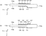
Fig. 9 is the general view of structure that the vibrating reed of present embodiment is shown.Figure 10 is the general view at Fig. 9 back side of structure that the vibrating reed of present embodiment is shown.Figure 11 is the summary section along C-C line among Fig. 9 that the structure of piezoelectric element is shown.Figure 12 is the summary section along D-D line among Fig. 9.
As shown in Figure 9 and Figure 10, vibrating reed 2 uses the base material of quartz or silicon etc. to form.The form of vibrating reed 2 is: when launched on the XY plane in orthogonal coordinate system, the Z direction was thickness.Vibrating reed 2 has 3 shaker arms 111,112,113, and shaker arm 111,112,113 is arranged side by side at directions X, and extends in parallel to each other on Y-direction.And shaker arm 111,112,113 is connected on the base portion 115, consists of each shaker arm 111,112,113 and is the vibrating reed 2 of cantilever design.And shaker arm 111,112,113 conduct are relative with the 2nd 116b with the 1st 116a of the face of Z perpendicular direction, and the size block between the 1st 116a and the 2nd 116b is made shaker arm 111,112,113 thickness.
Position at each shaker arm 111,112,113 close base portion 115 is formed with respectively piezoelectric element 161,162,163.
As shown in figure 11, the piezoelectric element 161 that is formed on the shaker arm 111 forms by stacked lower electrode 121, piezoelectric film 131 and upper electrode 151.
Lower electrode 121 is arranged on the 1st 116a in the relative face of thickness of regulation shaker arm 111.And the distribution 128 that is connected with lower electrode 121 is led to the 2nd 116b to surround the mode of shaker arm 111 via the side of shaker arm 111.On lower electrode 121, be formed with piezoelectric film 131 in the mode that covers lower electrode 121, this piezoelectric film 131 will surround around the shaker arm 111.And, be provided with upper electrode 151 at the position that is positioned at above the lower electrode 121 on the piezoelectric film 131.
Like this, across piezoelectric film 131 and relative mode forms piezoelectric element 161, by to applying generating positive and negative voltage between each electrode, can make piezoelectric film 131 compressions or elongation with lower electrode 121 and upper electrode 151.And, by making piezoelectric film 131 compressions or elongation, shaker arm 111 is subjected to displacement in the Z direction.
Equally, piezoelectric element 162, the 163rd, by stacked lower electrode 122,123, piezoelectric film 132,133 and upper electrode 152,153 form.And the distribution 128 that is connected with lower electrode 122,123 is led to the 2nd 116b side via shaker arm 112,113 side.
In addition, lower electrode 121,122,123, upper electrode 151,152,153 and the distribution 128, the 158th that is connected with these electrodes form continuously, thereby in description of the present embodiment, lower electrode 121,122,123 and upper electrode 151,152,153 refer to these electrodes across piezoelectric film 131,132,133 and overlapping part, part in addition is called as the distribution 128,158 that is connected with each electrode.
In addition, can lower electrode 121,122,123 and upper electrode 151,152,153 between SiO is set
2, Si
2N
3Deng dielectric film, with this prevent reliably lower electrode 121,122,123 and upper electrode 151,152,153 between electrical short.
Then, such as Fig. 9, Figure 10, shown in Figure 12, the distribution 128 that is connected with lower electrode 121,122,123 and the distribution 158 that is connected with upper electrode 151,152,153 are led to the base portion 115 of vibrating reed 2 and are connected with installing electrodes 165,166, this installing electrodes 165,166 is fixed on the pedestal of encapsulation etc., is used for realizing conducting.In addition, be provided with lower electrode 121,123 connecting portions 157 that are connected with upper electrode 152 so that piezoelectric element 161,163 with piezoelectric element 162 between polarity opposite.
In addition, lower electrode and upper electrode can use the metal materials such as Au, Al, Ti.And, lower electrode and upper electrode can and bottom between be equipped with the Cr film, be used for improving and bottom between dhering strength.As piezoelectric film, can use ZnO, A1N, PZT, LiNbO
3, KNbO
3Deng material, but because ZnO and AlN can access better characteristic, thereby be particularly preferred.
In addition, in the situation of using quartz as the base material of vibrating reed 2, can use X septum, AT septum, Z septum etc.
The structure of<the distribution that is connected with upper electrode with lower electrode>
Below, describe the distribution that is connected with upper electrode with the lower electrode of above-mentioned vibrating reed 2 in detail.
Figure 13 shows the distribution that is connected with lower electrode, and Figure 13 (a) is positive general view, and Figure 13 (b) is the general view at the back side.The distribution that Figure 14 shows upper electrode and is connected with upper electrode, Figure 14 (a) are positive general views, and Figure 14 (b) is the general view at the back side.
At first, as shown in figure 13, lower electrode 121,122,123 is arranged on the 1st 116a in the relative face of regulation shaker arm 111,112,113 thickness.
In the front of vibrating reed, shown in Figure 13 (a), the lower electrode 121,123 from the shaker arm 111,113 that is formed on the both sides that are positioned at shaker arm 112 is to base portion 115 wiring leads 128, and couples together with connecting portion 127.
On the other hand, at the back side of vibrating reed, shown in Figure 13 (b), from being formed on lower electrode 122 on the shaker arm 112 that is positioned at central authorities to base portion 115 wiring leads 128, and couple together with installing electrodes 166.This installing electrodes 166 is directed to the front of vibrating reed by the distribution on the side that is formed on base portion 115, be provided with installing electrodes 166 at front and back.
And, from being formed on base portion 115 wiring leads 128 of lower electrode 121 on the same face on the shaker arm 111, and couple together with installing electrodes 165.This installing electrodes 165 is directed to the front of vibrating reed by the distribution on the side that is formed on base portion 115, be provided with installing electrodes 165 at front and back.
And upper electrode 151,152,153 is formed on the position of lower electrode 121,122,123 top.
As shown in figure 14, from being formed on base portion 115 wiring leads 158 of upper electrode 152 on the same face on the shaker arm 112 that is positioned at central authorities, and couple together with connecting portion 157.Base portion 115 wiring leads 158 of upper electrode 151 from the shaker arm 111,113 that is formed on the both sides that are positioned at shaker arm 112,153 on the same face, and be connected, and these distributions 158 are connected with installing electrodes 166.And, shown in Figure 14 (b), on another side (back side), do not form distribution.
Consisted of like this with lower electrode 121,122,123 are connected with upper electrode, 152,153 distributions that are connected 128,158, the connecting portion 127 of lower electrode side is connected with the connecting portion 157 of upper electrode side, lower electrode 121,123 is connected with upper electrode 152.And, be connected with installing electrodes 165 by lower electrode 121.Like this, formed lower electrode 121,123 has been connected the distribution that is connected with installing electrodes 165 with upper electrode.
And the installing electrodes 166 of lower electrode side is connected with the installing electrodes 166 of upper electrode side, and lower electrode 122 is connected with upper electrode 151,153.Like this, formed with lower electrode 122 are connected with upper electrode, 153 distributions that are connected with installing electrodes 166.
In the vibrating reed 2 of said structure, with illustrated the same of Fig. 7, by applying voltage to each piezoelectric element, shaker arm is subjected to displacement in the Z direction.And, because shaker arm 111 and shaker arm 113 are provided with the piezoelectric element of identical polar, thereby the shaker arm 111,113 of the shaker arm 112 of central authorities and its both sides vibrates in the opposite direction, carry out as follows vibration (walking mode vibration) by applying alternating voltage, that is: adjacent shaker arm alternately repeatedly carries out rightabout vibration.
Above, in the vibrating reed 2 of present embodiment, the distribution 128 that is connected with lower electrode 121,122,123 to be surrounding each shaker arm 111,112,113 mode, led to shaker arm 111,112,113 the 2nd 116b via shaker arm 111,112,113 side from shaker arm 111,112,113 the 1st 116a.
From shaker arm 111,112,113 the 1st 116a to the 2nd 116b wiring lead 128 as its back side, can easily distribution 128 be led to the back side by in this wise.And, because can be with the front and back of vibrating reed all for the configuration of distribution 128, thereby, enlarged 128 areas that can configure of distribution, increased the configuration degree of freedom of distribution 128.And, even in limited space, also can configure distribution 128, can realize the miniaturization of vibrating reed 2.
(variation)
In addition, even the vibrating reed that the thickness of base portion forms thicklyer than the thickness of shaker arm also can utilize the configuration of electrode and the distribution of present embodiment.
Figure 15 is the summary section that the variation of the vibrating reed that the thickness of base portion forms thicklyer than the thickness of shaker arm is shown.This profile is and the corresponding section of above-mentioned Figure 12.
In this variation, the flat shape of vibrating reed, the upper electrode, piezoelectric film, lower electrode and the distribution that are formed on the vibrating reed adopt the structure identical with the 2nd execution mode, and only the section shape of vibrating reed is different.
In the following description, the inscape identical with the 2nd execution mode enclosed same numeral, description thereof is omitted.
For the vibrating reed shown in Figure 15 (a), the 1st 116a side at shaker arm 112a, have the smooth face from shaker arm 112a to base portion 115a, in the 2nd the 116b side of shaker arm 112a, the inclined plane part 117 that forms via the part at base portion 115a is connected with shaker arm 112a.Like this, by the 2nd 116b side at shaker arm 112a inclined plane part 117 is set, the thickness of vibrating reed forms the end thickening continuously from shaker arm 112a to base portion 115a.And, dispose the distribution 128 that is connected with lower electrode 122 at this inclined plane part 117.
For the vibrating reed shown in Figure 15 (b), the 1st 116a side at shaker arm 112b, the inclined plane part 117 that forms via the part at base portion 115b is connected with shaker arm 112b, in the 2nd the 116b side of shaker arm 112b, the inclined plane part 117 that forms via the part at base portion 115b is connected with shaker arm 112b.Like this, by the 1st 116a side and the 2nd 116b side at shaker arm 112b inclined plane part 117 is set, the thickness of vibrating reed forms the end thickening continuously from shaker arm 112b to base portion 115b.And, dispose the distribution 128 that is connected with lower electrode 122 and the distribution 158 that is connected with upper electrode 152 at this inclined plane part 117.
As mentioned above, form than the thickness of shaker arm in the thick vibrating reed at the thickness of base portion, the coupling part with shaker arm 112a, 112b of base portion 115a, 115b forms inclined plane part 117, and the distribution 128,158 that is directed to base portion 115a, 115b from shaker arm 112a, 112b is connected with installing electrodes etc. through these inclined plane parts 117.
For above-mentioned like that in the situation that do not form inclined plane part 117 with shaker arm for situation that base portion is connected, at the boundary generation step of shaker arm and base portion.And in this variation, owing to having inclined plane part 117 in the coupling part, thereby compare with the situation that occurs to intersect at step place distribution 128,158, distribution 128,158 can not occur and intersect the situation of corner angle of acute angle, can prevent the distribution 128 at this part place, 158 broken string.And, since there is not step in the coupling part of shaker arm and base portion, therefore, in the situation that form distribution 128,158 with photoetching technique, can carry out reliably the exposure of resist, can easily form distribution 128,158 in the situation that the distribution broken string does not occur.
In addition, in the 1st execution mode and the 2nd execution mode, the vibrating reed with 3 shaker arms has been described, but, the quantity of shaker arm is not limited to these execution modes, can be more than 3, is preferably the odd number more than 3.
(the 3rd execution mode)
Below, as the 3rd execution mode, the oscillator of the vibrating reed with above-mentioned explanation is described.
Figure 16 shows the structure of oscillator, and Figure 16 (a) is general view, and Figure 16 (b) is the summary section along G-G line among Figure 16 (a).
Oscillator 5 has: vibrating reed 1, as ceramic packaging 81 and the lid 85 of receptacle.
Ceramic package 81 is formed with recess in the mode that can take in vibrating reed 1, is provided with the connection pad 88 that is connected with the installing electrodes of vibrating reed 1 in this recess.Connecting pad 88 constitutes: be connected with the distribution in the ceramic package 81, and can with the peripheral part that is arranged on ceramic package 81 on external connection terminals 83 conductings.
And, around the recess of ceramic packaging 81, be provided with endless loop 82.And, be provided with through hole 86 in the bottom of ceramic package 81.
Vibrating reed 1 is adhesively fixed on by conductive adhesive 84 on the connection pad 88 of ceramic packaging 81, and the lid 85 of the recess that covers ceramic packaging 81 is stitched weldering with endless loop 82.In the through hole 86 of ceramic packaging 81, be filled with the encapsulant 87 of metal material.Sealing material 87 melts in reduced atmosphere, and ceramic packaging 81 interior gas-tight seals are become decompression state.
Like this, the 1st execution mode of oscillator 5 or the vibrating reed of the 2nd execution mode are housed in the ceramic packaging 81, and the oscillator 5 of easy miniaturization and characteristic good can be provided.
In addition, can also in ceramic packaging 81, accommodate the circuit element of IC of comprising oscillating circuit etc. and constitute oscillator.