CN101740494B - Transfer method of functional region, led array, led printer head, and led printer - Google Patents
Transfer method of functional region, led array, led printer head, and led printer Download PDFInfo
- Publication number
- CN101740494B CN101740494B CN2009102115367A CN200910211536A CN101740494B CN 101740494 B CN101740494 B CN 101740494B CN 2009102115367 A CN2009102115367 A CN 2009102115367A CN 200910211536 A CN200910211536 A CN 200910211536A CN 101740494 B CN101740494 B CN 101740494B
- Authority
- CN
- China
- Prior art keywords
- substrate
- functional area
- layer
- transfer method
- zone
- Prior art date
- Legal status (The legal status is an assumption and is not a legal conclusion. Google has not performed a legal analysis and makes no representation as to the accuracy of the status listed.)
- Expired - Fee Related
Links
Images


Classifications
-
- H—ELECTRICITY
- H01—ELECTRIC ELEMENTS
- H01L—SEMICONDUCTOR DEVICES NOT COVERED BY CLASS H10
- H01L27/00—Devices consisting of a plurality of semiconductor or other solid-state components formed in or on a common substrate
- H01L27/15—Devices consisting of a plurality of semiconductor or other solid-state components formed in or on a common substrate including semiconductor components with at least one potential-jump barrier or surface barrier specially adapted for light emission
- H01L27/153—Devices consisting of a plurality of semiconductor or other solid-state components formed in or on a common substrate including semiconductor components with at least one potential-jump barrier or surface barrier specially adapted for light emission in a repetitive configuration, e.g. LED bars
-
- B—PERFORMING OPERATIONS; TRANSPORTING
- B41—PRINTING; LINING MACHINES; TYPEWRITERS; STAMPS
- B41J—TYPEWRITERS; SELECTIVE PRINTING MECHANISMS, i.e. MECHANISMS PRINTING OTHERWISE THAN FROM A FORME; CORRECTION OF TYPOGRAPHICAL ERRORS
- B41J2/00—Typewriters or selective printing mechanisms characterised by the printing or marking process for which they are designed
- B41J2/435—Typewriters or selective printing mechanisms characterised by the printing or marking process for which they are designed characterised by selective application of radiation to a printing material or impression-transfer material
- B41J2/447—Typewriters or selective printing mechanisms characterised by the printing or marking process for which they are designed characterised by selective application of radiation to a printing material or impression-transfer material using arrays of radiation sources
- B41J2/45—Typewriters or selective printing mechanisms characterised by the printing or marking process for which they are designed characterised by selective application of radiation to a printing material or impression-transfer material using arrays of radiation sources using light-emitting diode [LED] or laser arrays
-
- H—ELECTRICITY
- H01—ELECTRIC ELEMENTS
- H01L—SEMICONDUCTOR DEVICES NOT COVERED BY CLASS H10
- H01L33/00—Semiconductor devices with at least one potential-jump barrier or surface barrier specially adapted for light emission; Processes or apparatus specially adapted for the manufacture or treatment thereof or of parts thereof; Details thereof
- H01L33/005—Processes
- H01L33/0093—Wafer bonding; Removal of the growth substrate
Abstract
A method includes placing a first bonding layer on at least one of a first functional region bonded on a release layer with a light releasable adhesive layer on a first substrate, and a transfer region on a second substrate; bonding the first functional region to the second substrate by the first bonding layer; irradiating the release layer with light with a light blocking member being provided to separate the first substrate from the first functional region at the release layer; placing a second bonding layer on at least one of a second functional region on the first substrate, and a transfer region on the release layer or a transfer region on a third substrate; bonding the second functional region to the second substrate or the third substrate by the second bonding layer; and separating the first substrate from the second functional region at the release layer.
Description
Technical field
The present invention relates to be used to make transfer (transfer) method of the functional area of semiconductor device, semiconductor product, semiconductor device etc.And, the present invention relates to light-emitting diode (LED) array, LED printing head and the LED printer made through transfer method.
Background technology
The technology that the formation layer of the light-emitting diode that will on the GaAs substrate, form via sacrifice layer is transferred to silicon substrate is known.United States Patent(USP) No. 6913985 discloses this technology.More specifically, the formation layer that is deposited on the light-emitting diode on the GaAs substrate via sacrifice layer at first is divided into a plurality of light-emitting zones through forming groove therein.Sacrifice layer is exposed to groove.Then, dry film photoresist is attached to the formation layer of light-emitting diode, and, the support component of joint (bond) net metal line on dry film photoresist.
Then, the part of the resist beyond the part under the net metal line is removed.Through the mesh-supported parts sacrifice layer is contacted with the etch sacrificial layer with etchant.Therefore, the GaAs substrate separates with composite construction.And, the GaAs substrate separately after, engage silicon substrate having on the light-emitting diode that constitutes layer.Have the light-emitting diode that constitutes layer and be transferred to silicon substrate.
The open No.2003-174041 of Japan Patent discloses the chip that will be selected from a plurality of semiconductor chips that form on the substrate and partly has been placed into the technology on another substrate.More specifically, be prepared in first laminated construction that forms on first substrate, and be prepared in second laminated construction that forms on second substrate with separating layer (release layer) with device layer.Then, face each other, first laminated construction and second laminated construction are engaged through making device layer and separating layer.The laminated construction that comprises device layer and separating layer is divided into a plurality of parts with predetermined pattern.Thus, on second substrate, form a plurality of chips that comprise device.The predetermined chip that is selected from said a plurality of chips is engaged to the precalculated position on the 3rd substrate.Then, second substrate separates with selected chip at the separating layer place, and selected chip is placed on the 3rd substrate thus.
Through using compound semiconductor on the GaAs substrate to make under the situation of led array etc. such as GaAs and since with the silicon substrate GaAs substrate of comparing be expensive, so effective use of GaAs substrate is useful.And; In the size of GaAs substrate (for example; 2 inches, 4 inches, 6 inches or 8 inches substrates) with the size of silicon substrate (for example; 4 inches, 5 inches, 6 inches, 8 inches or 12 inches substrates) under the condition of different, when each substrate unit collectively or together carries out when shifting, transferable zone is the zone of less substrate.Therefore, in order to obtain effective transfer, make the size of the less substrate of size conforms of two substrates.
Carrying out with disclosed mode in like United States Patent(USP) No. 6913985 when shifting, available GaAs semiconductor layer only be with silicon substrate on the corresponding part of device that forms.Therefore, with silicon substrate on device between the corresponding GaAs semiconductor of part go out of use need not.
To said circumstances be described with reference to Figure 19 A and Figure 19 B.Figure 19 A and Figure 19 B are illustrated in circuit devcie that forms on the silicon substrate and the luminescent device layer that on the GaAs substrate, forms respectively.Reference numeral 11 expression GaAs substrates, the luminescent device layer of Reference numeral 12 expression GaAs, Reference numeral 13 expression silicon substrates, Reference numeral 14 is illustrated in the circuit devcie that forms on the silicon substrate 13.Can obtain luminescent device through luminescent device layer 12 is transferred on the circuit devcie 14.Luminescent device layer 12 is placed on the part of circuit devcie 14 or near the part of circuit devcie 14.For example, the size of luminescent device layer 12 is about 10mm*50 μ m.In contrast, for example, the size of circuit devcie 14 is about 10mm*0.3mm.Therefore, transferred to by collective under the situation on the circuit devcie 14 at luminescent device layer 12, the layout of luminescent device layer 12 and transferable quantity are owing to the layout of circuit devcie 14 is restricted.Therefore, to tend to be little to the usable area of the luminescent device layer 12 of every GaAs substrate 11 unit ares.
On the other hand, according to the technology of the open No.2003-174041 of Japan Patent, on first substrate, form a large amount of chips, and being selected property of the part transfer of chip is on second substrate.Therefore, can form on first substrate with a plurality of second substrates on the corresponding chip of transfer portion.Therefore, can effectively use first substrate to a certain extent.But according to this technology, when the transfer of being selected property of chip, adhesive is deposited over the chip that is used to shift.Therefore, there is the possibility that following situation occurs.When chip size little (for example, width is less than the hundreds of micron), adhesive maybe be from (intended) chip projection of estimating.In this case, the chip of non-expectation possibly also be engaged, and, disadvantageous transfer can appear.As a result, output possibly reduce.
And along with chip size reduces, the thickness of adhesive will be set as and approach, and makes the not chip projection from estimating of adhesive.If under this condition, carry out joining process, possibly make the chip and second substrate contacts of non-expectation so, and therefore some damages can occur.
Summary of the invention
According to an aspect; The present invention provides a kind of method, and this method comprises: will shift first knitting layer of arranging predetermined thickness at least one in the zone of first functional area being bonded on first substrate to it on first functional area and second functional area and second substrate on the separating layer; Make first functional area and second substrates through first knitting layer; Be provided with under the state of light-blocking member with the said separating layer of rayed; At said separating layer place first substrate and first functional area are separated, said light-blocking member is used to block the light towards the zone except the zone that has first functional area on it on first substrate; To shift second knitting layer of arranging predetermined thickness at least one in the zone of second functional area will shift on second functional area on first substrate and second substrate to it on zone or the 3rd substrate of second functional area to it; Make second functional area and second substrate or the 3rd substrates through second knitting layer; And make said separating layer stand rayed or variations in temperature, first substrate and second functional area are separated at said separating layer place.
From with reference to the following description of accompanying drawing to exemplary embodiment and example, further characteristic of the present invention will become obvious.
Description of drawings
Figure 1A to Fig. 1 C is the sectional view that illustrates according to the step of preparation first substrate among the embodiment of transfer method of the present invention.
Fig. 2 A and Fig. 2 B are the sectional views that illustrates according to forming the step of knitting layer among the embodiment of transfer method of the present invention.
Fig. 3 A and Fig. 3 B are the sectional views that illustrates according among the embodiment of transfer method of the present invention the first functional area selectivity on first substrate being transferred to the step of second substrate.
Fig. 4 A and Fig. 4 B are the sectional views that illustrates according among the embodiment of transfer method of the present invention the second functional area selectivity on first substrate being transferred to the step of the 3rd substrate.
Fig. 5 A and Fig. 5 B are the sectional views that illustrates according among another embodiment of transfer method of the present invention the first functional area selectivity on first substrate being transferred to the step of second substrate.
Fig. 6 A and Fig. 6 B are the sectional views that illustrates according among another embodiment of transfer method of the present invention the second functional area selectivity on first substrate being transferred to the step of the 3rd substrate.
Fig. 7 A and Fig. 7 B are the sectional views that illustrates according among the another embodiment of transfer method of the present invention the second functional area selectivity on first substrate being transferred to the step of the 3rd substrate.
Fig. 8 A is the plane graph that a plurality of transfer expections (expected) zone on second substrate is shown.
Fig. 8 B is the plane graph that a plurality of functional areas on first substrate are shown.
Fig. 9 is the sectional view that the combination of separating layer patterned on the surface of first substrate is shown.
Figure 10 is the sectional view that illustrates according to the step of preparation first substrate in first example of transfer method of the present invention.
Figure 11 is the plane graph that obtains through the a1-b1 cross section of watching Figure 10 from a side.
Figure 12 is the plane graph that obtains through the a2-b2 cross section of watching Figure 10 from a side.
Figure 13 is a decomposition diagram of arranging the mode of island compound semiconductor lamination between position relation and the groove in semiconductor substrate between the groove that illustrates in first groove and the semiconductor substrate.
Figure 14 A to Figure 14 D is the sectional view that illustrates according to the step of preparation first substrate in second example of transfer method of the present invention.
Figure 15 is the perspective view that the example of LED printing head is shown.
Figure 16 illustrates the direct drive circuit that in the Si substrate, forms and the sectional view of LED device ways of connecting.
Figure 17 illustrates to be made the plane graph of the diminishbb light-emitting element array circuit of quantity of electrode by driving with time-sharing format.
Figure 18 A is the diagrammatic sketch of configuration that the example of LED printer is shown.
Figure 18 B is the diagrammatic sketch of configuration that the example of LED color printer is shown.
Figure 19 A is the plane graph that a plurality of transfer expected areas on the substrate in the conventional example are shown.
Figure 19 B is the plane graph that a plurality of functional areas on the seed substrate in the conventional example (seed substrate) are shown.
Embodiment
Below embodiment of the invention will be described with reference to drawings.In this manual, functional area typically is meant the zone that comprises semiconductor junction.This zone can be device.And functional area can be for having the zone of piezoelectric property, insulation property, magnetic property etc., such as the zone that can be used as the function element with electric or magnetic function.In any case; Key point of the present invention is: functional area is through separating layer and substrates; Said separating layer comprises the material that its bond strength is reduced by rayed, and, through under the state of light-blocking member separating layer being carried out rayed and carries out separately being provided with at the separating layer place.Based on above inventive concept, basic transfer method of the present invention comprises first to the 6th above-mentioned step.
To describe these steps in detail.At first in first step, prepare first substrate.Figure 1A to Fig. 1 C illustrates the step that preparation has first substrate 100 of functional area.In the present embodiment, shown in Figure 1A to Fig. 1 C, transfer to each the inclusion compound semiconductor layer 106 first and second functional areas 101 and 102 of first substrate 100 from the compound semiconductor substrate 103 of seed substrate.And each in first and second functional areas 101 and 102 comprises the etch sacrificial layer 105 and compound semiconductor layer 106 that on compound semiconductor substrate 103, forms successively.Here, on the compound semiconductor layer on the substrate 103 106, form resist layer 107 and it is carried out composition, and, the part between patterned resist layer 107 etchings, first and second functional areas 101 and 102 used, to form first groove 110.Thus, first and second functional areas 101 of island and 102 are separated from each other.
And, form second groove 111 (this finally becomes through hole) at least one in first substrate 100 and compound semiconductor substrate 103.Second groove 111 is formed with first groove 110 and is connected.In the present embodiment, in as the compound semiconductor substrate 103 of GaAs substrate, form second groove 111.Pass through NH
4OH+H
2O
2Etchant and/or DeepRIE (reactive ion etching) carry out the etching of GaAs.First substrate 100 is transparency carriers of glass etc.Compound semiconductor layer 106 in first and second functional areas 101 and 102 can comprise Bragg reflection (DBR) layer and the LED layer of distribution, and etch sacrificial layer 105 can be for the AlAs layer etc.
As seed substrate 103, can use GaAs substrate, p type GaAs substrate, n type GaAs substrate, InP substrate, SiC substrate, GaN substrate etc.And, replace above compound semiconductor substrate, can also use sapphire substrate, Ge substrate etc.Etch sacrificial layer 105 is can be with the etched layer of the etching speed faster than compound semiconductor lamination.As stated, the etch sacrificial layer 105 in the present embodiment is AlAs layer or AlGaAs layer (for example, Al
0.6Ga
0.4As).At the AlGaAs layer is Al
xGa
1-xUnder the situation of As layer (x be equal to or less than (1) and be equal to or greater than 0.6), when x was equal to or greater than 0.6, etching selectivity was significant.At the etch sacrificial layer is under the situation of AlAs layer, and the HF solution that can use (2) 2 percent to percent 10 the scope of being diluted to is as etchant.
At seed substrate 103 is under the situation of sapphire substrate, can use metal nitride layer such as chromium nitride (CrN) as the etch sacrificial layer.In this case, can be on chromium nitride epitaxial growth be used to make the function lamination of the device (as LED or laser) that is used for blueness or ultra-violet radiation.In lamination, can use GaInN that is used as active (active) layer and AlGaN or the GaN that is used as distance piece (spacer) layer.Etchant as the sacrifice layer that is used for chromium nitride (CrN) etc. can use common Cr etchant (chromium etching solution etc.).
Shown in Figure 1B, compound semiconductor substrate 103 is ground (lap) from basal surface, makes second groove 111 run through (penetrate) substrate 103.And first substrate 100 engages with first and second functional areas 101 and 102 on the compound semiconductor substrate 103 through separating layer 115, and said separating layer 115 comprises its bond strength by the material of rayed reduction.Here; Though in Figure 1A to Fig. 1 C, in compound semiconductor substrate 103, form second groove 111; But, since the substrate 100 of GaAs substrate and glass etc. compare be highly brittle and physical strength relatively a little less than, therefore in substrate 100, can easily form second groove on the contrary.Second groove in Figure 1A in the substrate 100 is illustrated by the broken lines.
In the present embodiment, separating layer 115 comprises the first separating layer 115a and the second separating layer 115b.The first separating layer 115a is a separable adhesive layer of lip-deep UV that is attached to sheet (sheet) base material 115c, and the reduction of its decomposition or bond strength takes place owing to the UV rayed.The second separating layer 115b is the separable adhesive layer of another lip-deep heat that is attached to flat substrates 115c, and the reduction of its decomposition or bond strength takes place owing to variations in temperature.And light shield layer 117 is set on first substrate 100 and the regional corresponding surface second functional area 102.Can be through formation light shield layers 117 such as vacuum evaporation.Replace light shield layer 117, also can use masterplate (stencil) mask that easily to place and to peel off.And, in the following steps that are described below, can come optionally to carry out the UV irradiation through for example assembling and scan the laser of UV wavelength (300nm to 400nm) for the desired area of the separable adhesive layer of UV.In this case, need not use light shield layer.
Be arranged under the situation in first substrate 100 at second groove, groove can form as follows.At first substrate is under the situation of silicon substrate, can be at SF
6Deng atmosphere in form the groove that runs through of second groove through the RIE that uses fluorine.Free radical species (radical species) are not limited to fluorine.Under the situation of wet etching, can use NaOH, KOH, TMAH etc.More specifically, after separating layer 115 is placed on the surface of silicon substrate 100, on another surface of silicon substrate 100, be formed for forming the mask layer of the resist of groove, and, use this mask in silicon substrate, to form groove.Though can use dry ecthing or wet etching, also can use sandblast etc. as RIE.In sandblast, the minuteness particle of quartz etc. is jetted to exposing on the position, physically to destroy a part of of silicon substrate and to form groove.For example, can in the thick silicon wafer of hundreds of micron, form this groove that runs through.In this formation that runs through groove, its sidewall can be protected, the feasible deterioration that its aspect ratio (aspect ratio) do not take place.And this method also can easily be applied to glass substrate etc.Therefore, replace above chemical etching, also can carry out the formation that runs through groove through the method for blasting method or winding-up fluid energy.Also can use laser brill or little brill to form groove.
As stated, can be prepared in the compound semiconductor layer 106 board structure that forms first groove 110, and formation is connected with first groove 110 at least one in substrate 100 and seed substrate 103 second runs through groove 111.Figure 1B representes this board structure.
Then, etchant is contacted with etch sacrificial layer 105, so that etch sacrificial layer 105 is carried out etching through first and second grooves 110 and 111.Compound semiconductor substrate 103 is thus with functional area 101 with opened in 102 minutes.That kind preparation shown in Fig. 1 C has first substrate 100 of first and second functional areas 101 and 102.The compound semiconductor substrate 103 that separates thus can be re-used, to have the functional area of compound semiconductor layer above the new formation.Under the dark situation of first groove 110 or groove 111, the bubble of the gas (hydrogen) that produces when existing in the etch sacrificial layer of etching AlAs etc. can stop up the possibility of the outlet of (close) groove.In this case, can apply ultrasonic wave to etchant or compound semiconductor substrate continuously or off and on.And, can add lubricant or the alcohol that is used to reduce angle of wetting to etchant (for example, hydrofluoric acid), with the bubble during inhibition or the removal etch processes.
As described in following Example, prepare on it method that is provided with first substrate of functional area via separating layer and be not limited to above method.For example, can be through jetting fluid so that substrate 103 prepares first substrate from its method of separating to the side of the interface of board structure separates layers or near it.
In next step, the knitting layer 205 of predetermined thickness be attached to will the transfer of being selected property first functional area 101 and second substrate 200 on to shift at least one in the zone of first functional area 101 to it.In the present embodiment, shown in Fig. 2 A and Fig. 2 B, knitting layer 205 is placed on second substrate 200 of the silicon substrate with drive circuit.At first, shown in Fig. 2 A, on second substrate 200, form knitting layer 205 (for example, organic insulator).Then, only the transfer expected areas of first functional area 101 on second substrate 200 is carried out and utilized sheltering of resist 206.Shown in Fig. 2 B, carry out etching through chemical etching or RIE, only on the transfer expected areas of second substrate 200, forming knitting layer 205, and, wait removal resist 206 through fogging agent (asher).Here, the thickness of knitting layer 205 is about 2.0 microns, and its surface is by fully smoothing.Utilize this thickness, when first functional area 101 engages with knitting layer 205, can prevent the crunch of second functional area 102 for the surface of second substrate 200.
In the present embodiment, the thickness of knitting layer 205 is in 1.0 microns to 10 microns scope.For the thickness under 1.0 microns, engage effect and reduce.For the thickness on 10 microns; There is following possibility: after functional area is transferred to second substrate; When functional area utilized metal line and the drive circuit that on second substrate, forms etc. to be electrically connected, situation that wiring that step (step) locates destroys etc. took place.And, as required, shown in Fig. 2 B, the transfer method of present embodiment can be included in second substrate 200 except will on the surface in the zone it shifts the zone of first functional area 101, forming the step of predetermined concavo-convex (unevenness) 208.
Utilize this concavo-convex 208, even second functional area 102 also can effectively prevent the joint between second functional area 102 and the substrate 200 because the stress when engaging contacts with the surface of second substrate 200.For example, can form concavo-convex 208 through the over etching of when forming knitting layer 205, carrying out.Compare with the surface of knitting layer 205, concavo-convex 208 surface is enough coarse.For example, the smoothness R on the surface of knitting layer 205
Pv(maximum of concavo-convex peak-valley difference) under about 2nm, and, R
a(mean value of peak-valley difference) is under about 0.2nm.In contrast, concavo-convex 208 surface roughness R
PvCan be on about 2nm, and concavo-convex 208 Ra can be on about 0.2nm.
As stated, a plurality of island functional areas 101 and 102 are set on the separating layer 115 that is placed on first substrate 100.In the present example, on the surface of the above-mentioned zone on second substrate 200, form concavo-convex 208.
In the present embodiment, knitting layer 205 is formed by organic material.As organic material, can use polyimides etc.Also can use the epoxy radicals knitting layer.Replace above-mentioned organic material layer, also can use spin on polymers and organic spin-coating glass (SOG).In these materials, add methyl free radicals, ethyl radical, phenyl free radical etc. to the inorganic insulation oxide layer of picture silicon oxide layer, and increase plasticity (plasticity) thus.For example, on the silicon substrate of second substrate 200 and/or under the situation of middle formation circuit region, can carry out following processing.Use organic SOG, the insulating layer of silicon oxide that is used to increase the flatness on the circuit region is formed into preset thickness on second substrate 200, and patterned.Insulating layer of silicon oxide has given viscosity under 100 ℃ prebake temperature.
In the present example, this viscosity on the surface of the knitting layer 205 after the pre-bake treatment helps the joint in the following engagement step.Usually, adherence (viscosity) is considered to occur owing to be contained in the silanol group of the hydrolysis free radical in the organic insulating material (for example, spin on polymers), the alkoxyl of organic component etc.Owing under treatment temperature, carry out dehydration condensation, so these compositions can strengthen knot (junction) or bond strength between wafer or the device.About plasticity, the stability of the plasticity of the material under the non-hydrolysis radical pair high temperature (>400 ℃) among the organic principle has contribution.The key factor that engages is considered to surface and particle.Relevant with it, the existence of organic insulator that can be through having plasticity and adherence (tackiness) relaxes the lower floor (underlayer) that is used to have device architecture and the flatness of composition surface.
And about the influence of particle, the particle of some sizes can be embedded in the organic insulator owing to the plasticity of organic insulator.Therefore, can eliminate the influence of particle basically.When increasing bed thickness, plasticity also is used for the strain of loose greatly storage.When the amount of the organic principle that is used to increase plasticity less and when forming thick relatively layer (on (1) micron), the defective as crackle possibly appear.Owing to these reasons, when the amount of the organic principle in hydrolysis in being contained in organic SOG and the non-hydrolysis free radical is set as on about 1 (one) wt.%, can obtain suitable viscosity and plasticity.Therefore, also can be stable layer even have the layer of the thickness of micron dimension.
As stated, second substrate 200 for example be semiconductor substrate, silicon substrate, in its surface have oxide layer silicon wafer, provide the silicon wafer of circuit (for example, drive circuit) etc.Under the situation of making the semiconductor laminated LED of inclusion compound, drive circuit for example is the circuit that is used for drive controlling LED.Silicon substrate can be substrate and the so-called CZ wafer that has silicon epitaxial layers in its surface.Replace silicon substrate, also can use silicon-on-insulator (SOI) substrate.
Second step and third step will be described; In second step; First functional area 101 engages with second substrate 200 through first knitting layer 205; In third step,, first substrate 100 and first functional area were opened in 101 minutes through being used to block under the state of the light-blocking member 117 of the light in the zone except the zone of shifting first functional area to it on first substrate the rayed of separating layer being provided with.Shown in Fig. 3 A, be placed on first functional area 101 on the separating layer 115 on first substrate 100 with knitting layer 205 alignings with engage.Shown in Fig. 3 B, in third step, first substrate 100 was opened at the separable adhesive layer 115a place and first functional area of separating layer 115 in 101 minutes.In the present embodiment, separable adhesive layer 115a stands given processing and becomes separable.This given processing is the processing that is used to cause the reduction of the decomposition of separable adhesive layer or bond strength.Here, carry out the irradiation of UV light, with the decomposition that causes the separable adhesive layer 115a of UV or the reduction of bond strength from transparency carrier 100 sides.Therefore, first substrate 100 and first functional area were opened in 101 minutes.Because the existence of light-blocking member 117, therefore carrying out UV with second functional area, 102 corresponding parts and shining not to separable adhesive layer 115a.Therefore, this part of separable adhesive layer 115a remains unchanged, and shown in Fig. 3 B, second functional area 102 remains on first substrate 100.In third step, UV laser can be converged to fine hot spot (spot) and scanned.
Separating part 115 can have another configuration.For example, as shown in Figure 9, can on first substrate 100, adhere to separating layer 120 and 121 accordingly with first and second functional areas 101 and 102 respectively with different performance.For example, one is the separable adhesive layer of first radiation, and another is the separable adhesive layer of second radiation, and it is through decomposing with the irradiation of the light of the different wave length of the separable adhesive layer of first radiation or the reduction of bond strength.And, in this case, can on first substrate 100, arrange light-blocking member, make when the time with separable adhesive layer of radiation of rayed, can guarantee to prevent the rayed of another adhesive layer.
Replace to use sheet material, can on first substrate 100, form through vacuum evaporation etc. and have the separating layer or the part 115 of the first and second separable adhesive layers.More specifically, separating layer can be formed by the material that comprises heat foamable utricule (thermal foaming capsule).The separable jointing material of UV can be its crosslinked material that destroys owing to the UV energy exposure or comprise can be through absorbing the material of the utricule that UV light foams.The separable jointing material of heat can be REVALPHA (name of product of NITTO DENKO) etc.
The the 4th to the 6th step will be described.In the 4th step, arrange second knitting layer 305 will shift at least one in the zone of second functional area on second functional area 102 and the 3rd substrate 300 (this can be second substrate 200) that remain on first substrate 100 to it.In the 5th step, second functional area 102 engages with the 3rd substrate 300 through second knitting layer 305.In the 6th step, separating layer stands rayed or variations in temperature, so that first substrate 100 was opened at the separating layer place and second functional area in 102 minutes.
When second functional area 102 is transferred to the 3rd substrate 300, can carry out the processing substantially the same with the transfer that is used for first functional area 101.In other words, shown in Fig. 4 A, on the 3rd substrate 300, form second knitting layer 305 (for example, organic insulator), and, only carry out and utilize sheltering of resist layer for the transfer expected areas of second functional area 102 on the 3rd substrate 300.Then, carry out etching, on the zone of hope, to form knitting layer 305 through chemical etching or RIE.
Then, shown in Fig. 4 A, second functional area 102 is aimed at and is engaged with second knitting layer 305.Shown in Fig. 4 B, first substrate 100 was opened at the separable adhesive layer 115b place and second functional area in 102 minutes.Here, the hot separable adhesive layer 115b of separating layer 115 stands approximately the heating to 170 ℃, with the decomposition that causes hot separable adhesive layer 115b or the reduction of bond strength.Then, remove resist 107 through peeling off.
In the present embodiment, can also omit light shield layer 117, and carry out comprehensive rayed, the substrate 100 of winning can be opened at the separable adhesive layer 115a place and second functional area in 102 minutes.In this case, separating layer 115 can only comprise separable adhesive layer 115a.Perhaps, separable adhesive layer 115b also can be formed by the material that the reduction of decomposition or bond strength takes place when with rayed.
As stated, when second functional area 102 is transferred to the 3rd substrate, to shift second knitting layer that forms predetermined thickness at least one in the zone of second functional area to it on second functional area and the 3rd substrate that remain on first substrate.Then, carry out the step utilize second knitting layer 305 to make the step of second functional area 102 and the 3rd substrate 300 joints and first substrate 100 was opened at separating layer place and second functional area in 102 minutes.In this case, also can form predetermined concavo-convex 308 (the 7th steps) on the zone the zone of second functional area except shifting on the 3rd substrate 300 to it.
As stated, the first separable adhesive layer 115a and the second separable adhesive layer 115b can comprise when standing rayed and taking place during to the heating of giving fixed temperature to decompose or the material separately of the reduction of bond strength.In this case, third step comprises with the rayed step of the first separable adhesive layer scheduled time, and the 6th step is included in under the temperature on the fixed temperature the second separable adhesive layer being kept the step of the scheduled time.
With describing the transfer method that uses shading die board mask 217.In the method, separable adhesive layer 115a can comprise the material that the reduction of decomposition or bond strength takes place when standing rayed.Separable adhesive layer 115b can comprise the material that the reduction of decomposition or bond strength takes place when the heating that stands rayed or extremely give fixed temperature.Here, shown in Fig. 5 B, in third step, be set at die board mask 217 under the given lip-deep state of first substrate 100, carry out the rayed preset time.Thus, first functional area 101 that utilizes knitting layer 205 to engage with second substrate 200 can be opened with first transparency carrier in 100 minutes.Then, shown in Fig. 6 B, in the 6th step, be set under the state on the given surface (surface the part corresponding) execution rayed preset time at another die board mask 218 with the 3rd functional area 103 that does not shift from first substrate 100.Thus, second functional area 102 that utilizes knitting layer 305 to engage with the 3rd substrate 300 can be opened with first substrate in 100 minutes.
Comprise when standing at the second separable adhesive layer 115b and to take place to decompose or the material of the reduction of bond strength and on first substrate 100, no longer existing under the situation of functional area to fixed temperature, can execution graph 7A and Fig. 7 B shown in step.In other words; In the 6th step; Under the state of removing light-blocking member, separating layer 115 is maintained to the temperature preset time on the fixed temperature, so that first substrate 100 was opened with second functional area that utilizes knitting layer 305 to engage with the 3rd substrate 300 in 102 minutes.In the 6th step, can also carry out comprehensive irradiation, so that first substrate 100 was opened with second functional area that utilizes knitting layer 305 to engage with the 3rd substrate 300 at separable adhesive layer 115a place in 102 minutes.Then, remove resist 107 through peeling off.
Can on first substrate 100, arrange first and second functional areas 101 and 102 with the island-shaped pattern of any hope.Typically, that kind shown in Fig. 8 B is arranged first and second functional areas 101 and 102 of island on substrate 100 with predetermined spacing.In this case, for example, that kind shown in Fig. 8 A, the zone 405 that engage with first functional area 101 or be connected is disposed on second substrate 200 with predetermined spacing.
Zone 405 is to comprise the distance piece that is used for knitting layer 205 and the zone of CMOS chip area.In this configuration, first functional area 101 on having only first substrate 100 be transferred on second substrate 200 be used for the distance piece of knitting layer 205 time, if concern 1 to 3 below satisfying, can realize effectively so shifting.
L<or=L (concerning 1)
W>w (concerning 2)
W+S>w+s (concerning 3)
Shown in Fig. 8 A and Fig. 8 B; W is each the width in first and second functional areas on first substrate; L is the length of each functional area, and s is the distance between the functional area, and W is the width in the zone that will be connected with first functional area of transferring to second substrate; L is the length in the said zone on second substrate, and S is the distance between the said zone on second substrate.
In addition, concern that 4 to 6 also is favourable below satisfying.
L=L (concerning 4)
W=n*w (concerning 5)
W+S=n (w+s) (concerning 6)
Here, n is equal to or greater than 2 integer.Here, repeatedly (for example n time) optionally transferred to fine and close first functional area 101 that forms on first substrate 100 zone of the knitting layer 205 on second substrate 200.In this case, when the functional area of luminescent layer etc. was transferred to circuit devcie etc., the layout of functional area and adoptable quantity were not limited by the layout of circuit devcie so.Therefore, the area ratio that can be used for forming the seed substrate of luminescent layer etc. can be increased.Therefore, can effectively use compound semiconductor wafer, it is expensive that said compound semiconductor wafer is compared with silicon wafer.Can when making complicated multifunction device integrated circuit etc., obtain favourable economic effect.Here, second silicon substrate 200 shown in Fig. 8 A comprises the 3rd functional area 405 with CMOS chip, and first functional area 101 engages with the 3rd functional area through knitting layer 205 or is connected.Similarly, the 3rd substrate comprises the 4th functional area, and second functional area 102 engages with the 4th functional area through knitting layer.
And, on the seed substrate 103 shown in Figure 1A, can repeatedly alternately form etch sacrificial layer and compound semiconductor lamination.In this case, can repeat of the transfer of compound semiconductor lamination to first substrate.Also can repeatedly alternately form etching stopping layer, etch sacrificial layer and compound semiconductor lamination.In this case, the quantity that is used for epitaxially grown thermo-lag (hysteresis) number of times on the seed substrate is not for a plurality of.
And, can functional area that transfer to second substrate or the 3rd substrate be transferred to final tetrabasal fully.In this case, it is interim carrier substrate that second substrate or the 3rd substrate are similar to first substrate, rather than final transfer base substrate.In this transfer method, the step below carrying out.In second step, knitting layer and second substrates of first functional area through when standing given processing, becoming separable second separating layer.For example, the knitting layer 205 of the organic insulator among Fig. 3 A is replaced by the separating layer of the separating layer among the image pattern 1A 115.Then, carry out the 8th step to the ten steps.In the 8th step, the knitting layer of predetermined thickness be placed on tetrabasal with utilize in first functional area of second separating layer and second substrates at least one on.The formation of the formation of knitting layer and above-mentioned knitting layer is roughly similar.Do not carry out composition.In the 9th step, all functions zone passage knitting layer on second substrate engages with tetrabasal.In the tenth step, second substrate separates with functional area at the second separating layer place.Employed second separating layer can be or can not be that selectivity is separable, and structurally the separating layer than above-mentioned is simple thereby can make second separating layer.And the second interim substrate can be formed by the material with the materials similar of above-mentioned first substrate, and, can omit light shield layer.
In the method, a plurality of functional areas on interim first substrate 100 respectively being selected property transfer to a plurality of second interim substrates.Then, each final substrate is transferred in all functions zone on each second substrate fully.Though look like circuitous mode because the quantity of temporary base increases this method, under some situations, it can make that workflow is smooth and easy and can advance transfer effectively.
With the example of describing to transfer method, led array, LED printing head and LED printer.
To first example that comprise the step for preparing first substrate with functional area be described with reference to Figure 10 to Figure 13.In Figure 10, Reference numeral 1000 expression substrates (for example, the substrate of compound semiconductor substrate or Ge etc.).Reference numeral 1009 expression etching stopping layers, Reference numeral 1010 expression etch sacrificial layers, and, Reference numeral 1020 expression compound semiconductor laminations.Reference numeral 1025 expressions are used for the compound semiconductor lamination 1020 on the compound semiconductor substrate 1000 is divided into first groove of island areas.Etching stopping layer 1009 can be set as required.
And, Reference numeral 2000 expression first substrates (for example, silicon substrate), Reference numeral 2005 is illustrated in second groove that forms in first substrate 2000, and, Reference numeral 2010 expression separating layers.In separating layer 2010, form the 3rd groove 2006.The 3rd groove 2006 is connected with second groove 2005.In the present example, though the width of first groove 1025 shown in Figure 10 and spacing equal the width and the spacing of second groove 2005, can make the width of the groove 1025 of winning bigger than the width of second groove 2005.Because first groove 1025 should be connected with groove 2005, therefore can make that the width of compound semiconductor layer is narrower than the distance between the groove 2005 of through-silicon substrate 2000.First substrate 2000 is not limited to silicon substrate.As stated, it can be a glass substrate etc.
In Figure 10, for example, the width of first groove 1025 is to the hundreds of micron from several microns.And for example, the width of second groove 2005 is to the hundreds of micron from several microns.Second runs through groove 2005 can be on 50 microns, or on 100 microns, or on 200 microns, make and can easily introduce etchant.But it depends on the thickness of first substrate 2000.Confirm that the position of running through groove 2005 makes that it is important not reducing device area as far as possible.Therefore, run through groove 2005 the position can with have the line that chip separates width and aim at.Exist wire-bonded pad (pad) (referring to Figure 16) on the silicon circuit to occupy many situation of the area bigger than the device of silicon circuit.In this case, welding disking area can not become the zone to its transferring device.Therefore, when welding disking area was focused on the end of silicon circuit chip, the zone of first substrate corresponding with the welding disking area of concentrating can be used for forming ran through groove.
Figure 11 illustrates the cross section that obtains along the line a1-b1 among Figure 10.As obviously visible from Figure 11, compound semiconductor lamination 1020 is divided into the zone, island on compound semiconductor substrate 1000.The zone, island is from its peripheral region projection.Compound semiconductor lamination 1020 will be cut apart with the pattern of hope, and its segmented shape can be or can not be rectangular shape shown in figure 11 thus.First groove 1025 is the spaces between the zone, island of compound semiconductor lamination 1020.In Figure 11 to Figure 13, with among Figure 10 similarly key element by with Figure 10 in similarly Reference numeral represent.
Figure 12 illustrates the cross section that obtains along the line a2-b2 among Figure 10.As shown in Figure 12, in silicon substrate 2000, form groove 2005.Form semiconductor substrate groove 2005 betwixt with some suitable spacing.Owing to run through this layout of groove, for example, the rigidity of silicon wafer is deterioration so not.Therefore, in following processing, help handling.Figure 13 illustrates the mode of arranging the zone, island of compound semiconductor lamination 1020 in position relation and the part between the groove in semiconductor substrate 2,000 2005 between the groove 2005 in first groove 1025 and the semiconductor substrate.In Figure 13, separating layer 2010, etching stopping layer 1009 and etch sacrificial layer 1010 are omitted.As shown in Figure 13, when the parts of the parts of Figure 11 and Figure 12 when range upon range of, the island 1020 of projection arrives runs through the position between the groove 2005.
As long as the island 1020 of projection can be supported, this layout just is not limited to the layout shown in Figure 12 and Figure 13.For example, can be so that run through vertical quadrature on groove 2005 and the island 1020 of projection or make it and arrange with the island of projection 1020 crossing modes and to run through groove 2005.
In the present example, as stated, prepared the board structure that comprises seed substrate 1000, etch sacrificial layer 1010, compound semiconductor lamination 1020, separating layer 2010 and first substrate 2000.Can etchant be introduced in this structure through second groove 2005 and the 3rd groove 2006 that run through first substrate 2000 and separating layer 2010.Etchant is contacted with etch sacrificial layer 1010 with the execution etch processes, and seed substrate 1000 and board structure are separated.
Though first groove 1025 runs through etch sacrificial layer 1010, the first groove 1025 and can be used to or can not be used to run through etch sacrificial layer 1010 in Figure 10.It is important exposing etch sacrificial layer 1010 for etchant.
Only use etching stopping layer 1009 as required.Will accurately managing in time under the etched situation of carrying out degree, can omit etching stopping layer.
In above-mentioned transfer method, for example, when making LED, the compound semiconductor lamination below forming.Go up formation P-AlAs layer (etch sacrificial layer) at p type GaAs substrate (seed substrate), and following layer is formed the compound semiconductor lamination on the etch sacrificial layer.That is, deposition p type GaAs contact layer, p type AlGaAs covering (cladding layer), p type AlGaAs active layer, n type AlGaAs covering and n type GaAs contact layer.Between sacrifice layer and compound semiconductor substrate, can form AlInGaP as etching stopping layer.
When with sulfuric acid etchant GaAs layer and AlGaAs layer, be etched in AlInGaP layer place and stop.Then, remove the AlInGaP layer through hydrochloric acid.When with ammonia and hydrogen peroxide etching GaAs layer and AlGaAs layer, can use AlAs as stopping layer.
As the material of compound semiconductor lamination, replace above-mentioned GaAs system, can use for example AlGaInP system, InGaAsP system, GaN system, AlGaN system or InAlGaN system.
And, at least a in metal level and the DBR mirror (mirror) can be set on the compound semiconductor lamination.Metal level can be formed by for example Au, Ti or Al.Can select the material of metal level according to the emission wavelength of LED.When making the red colour system LED of 600nm to 800nm,, can use Au, Ag etc. as material with high reflectance.In the blueness near 360nm is under the situation of LED, can use Al.
The DBR mirror can comprise the structure that for example repeatedly alternately forms AlAs layer and AlGaAs layer for GaAs based compound semiconductor material.Perhaps, alternately form Al oxide skin(coating) and Al
0.2Ga
0.8The As layer.Since be difficult to form aluminum oxide through epitaxial growth, therefore can be through between 0.2 and 0.8, alternately changing Al
xGa
1-xThe value of x among the As is carried out the adjusting of refractive index.
And, when using the compound semiconductor lamination to make the LED device, replace heterojunction type LED, can adopt homogeneity junction type LED.In this case, after the layer that forms through epitaxial growth separately, the diffusion of impurities of carrying out through the solid-state diffusion method forms the pn knot in active layer.In order between contact layer and p side or n lateral electrode, to set up ohmic contact, contact can have than clip the high impurity concentration of covering of active layer.
And, in this first example, owing to have separating layer and light-blocking member, can transfer to another substrate with being selected property of high accuracy like the functional area on first substrate of preparation as described in top.
To second example that comprise the step for preparing first substrate with functional area be described with reference to Figure 14 A to 14D.In the step of Figure 14 A (the interface separates layers forms step and semiconductor layer formation step), on seed substrate 504, form semiconductor layer (for example, InGaAs) interface separates layers 505 as the Ge substrate through heteroepitaxial growth.The lattice constant of this semiconductor layer and/or thermal coefficient of expansion are different with substrate 504.Then, on interface separates layers 505, form the semiconductor layer 506 of GaAs etc.Separates layers 505 is corresponding with above-mentioned sacrifice layer.
In the engagement step shown in Figure 14 B, the semiconductor layer 506 on the seed substrate 504 engages with the separating layer 510 that on first substrate 507 of Si etc., forms, with acquisition composite construction 508.Separating layer 510 can be above-mentioned separating layer.
In the division step of Figure 14 C, produce the crackle that extends along direction in the surface in interface between interface separates layers 505 and/or interface separates layers 505 and semiconductor layer 506 and/or the interface between interface separates layers 505 and the seed substrate 504.Therefore, the semiconductor layer 506 and first substrate 507 were opened from composite construction in 508 minutes.In above-mentioned step, semiconductor layer 506 is transferred to first substrate 507 from seed substrate 504.Shown in Figure 14 D, can obtain to comprise the board structure 509 of first substrate 507 that has separating layer 510 and semiconductor layer 506 on it.
In above-mentioned step, produce in a concentrated manner because the strain energy that lattice constant and/or mismatch in coefficient of thermal expansion caused in interface between interface separates layers 505 and/or interface separates layers 505 and semiconductor layer 506 and/or the interface between interface separates layers 505 and the seed substrate 504.Then, apply separately valence for whole composite construction 508 or its part (for example, the interface between interface between interface separates layers 505 and/or interface separates layers 505 and the semiconductor layer 506 and/or interface separates layers 505 and the seed substrate 504).By means of the strain energy that in composite construction 508, produces, the semiconductor layer 506 and first substrate 507 can be opened from composite construction in 508 minutes.Form groove, semiconductor layer 506 is divided into a plurality of island functional areas.Before the engagement step of Figure 14 B, can form groove so that semiconductor layer 506 is divided into the island functional area.
Make the semiconductor layer and first substrate from the step that composite construction was opened in 508 minutes, can be near winding-up fluid W (liquid or gas) interface separates layers 505 or its.Injecting fluid W to above-mentioned position can crack in the injection part of composite construction, thereby causes above-mentioned separating.
And, in second example, owing to have separating layer and a light-blocking member, can transfer to another substrate with being selected property of high accuracy like the functional area on first substrate of preparation as described in top.
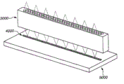
With the 3rd example of describing to the led array of making through above-mentioned transfer method.Can obtain the led array shown in Figure 15 through using above-mentioned transfer method.Figure 15 illustrates drive circuit and led array 4000 and is connected and is disposed in the structure on the printed circuit board (PCB) 5000.Can obtain drive circuit and led array in the following manner.On the silicon substrate shown in Fig. 8 A, form a plurality of LED devices, and, on printed circuit board (PCB) 5000, arrange through using cutting to cut apart a plurality of parts that silicon substrate obtains.The cross section structure of each LED device and each drive circuit is similar with the LED device and the drive circuit that comprise the LED light-emitting zone shown in the Figure 15 that describes below.
In the structure of Figure 15, the led array/drive circuit 4000 of many groups is arranged on wire ground (linearly) on printed circuit board (PCB) 5000.In led array/drive circuit 4000, the driver device of LED device and driver IC that kind shown in figure 16 is electrically connected.Can place bar-shaped (rod) lens arra 3000 (for example, SLA:Selfoc lens arra) in the face of led array 4000 as required.Therefore, can make the LED printing head.Assemble from the light of led array 4000 emissions of wire layout through rod type lens array 3000, to realize that through led array image forms.
Therefore constitute layer at the LED device and be formed on the silicon substrate and insert therebetween under the situation of metal level or DBR mirror, owing to the improvement of pointing capability can obtain fine hot spot.In this case, can not use rod type lens array and make up the LED printing head.
As shown in Figure 16, in the connection configuration between driver IC (drive circuit) and LED device, driver IC can directly be fabricated in silicon substrate, and is connected with the LED device.In the configuration of Figure 16, on silicon substrate 7000, form the insulating barrier 7010 (referring to the knitting layer 205 among Fig. 3 A and Fig. 3 B) of organic material with the MOS transistor 7060 that constitutes driver IC.The semiconductor laminated LED light-emitting zone 7070 of inclusion compound is set on insulating barrier 7010.And, Reference numeral 7080 another insulating barriers of expression, Reference numeral 7050 expressions form the source electrode of MOS transistor 7060 or the wire-bonded pad of drain region.For example, can make this configuration from the structure of second substrate 200 shown in Fig. 3 B.
Figure 17 illustrates the structure that is used for matrix driving.In order to reduce the quantity of electrode, can drive the light-emitting element array circuit 8500 among Figure 17 with the mode of timesharing.In Figure 17, Reference numeral 8011 expression n lateral electrodes, Reference numeral 8017 expression p lateral electrodes, the insulating barrier on the Reference numeral 8021 expression n type AlGaAs, the insulating barrier on the Reference numeral 8022 expression p type GaAs contact layers, Reference numeral 8023 expression light-emitting zones.
But the transfer method of the application of the invention is realized above-mentioned low-cost and high-performance led array and LED printing head.
Figure 18 A illustrates the example of the LED printer that uses above-mentioned LED printing head.The LED printer comprises LED printing head, photosensitive drums and electrostatic charging device.Image formation unit forms electrostatic latent image through using the light beam from the light source of LED printing head on photosensitive drums.
In Figure 18 A of the schematic sectional view of the configuration that the LED printer is shown, in printer body (body) 8100, place the photosensitive drums 8106 that can be rotated in a clockwise direction.On photosensitive drums 8106, arrange that LED printing head 8104 is used to the photosensitive drums of making public.LED printing head 8104 comprises and has each according to the led array 8105 of the luminous a plurality of light-emitting diodes of picture signal be used on photosensitive drums 8106, forming the rod type lens array 8101 of image of the radiation pattern of each light-emitting diode.Rod type lens array 8101 has above-mentioned configuration.The imaging plane that causes light-emitting diode through rod type lens array 8101 is surperficial consistent with photosensitive drums 8106.In other words, realize the optical conjugate relation between the photosensitive surface of radiating surface and photosensitive drums of light-emitting diode through rod type lens array.
Around photosensitive drums 8106, be provided for the electrostatic charging device 8103 of the surperficial uniform charging of photosensitive drums 8106 and be used for making toner be attached to photosensitive drums 8106 to form the developing device 8102 of toner image according to the exposing patterns of printing head 8104.Also be furnished with and be used for toner image is transferred to as the transfer printing electrostatic charging device 8107 of the transfer materials of copy sheet and is used to remain in after being collected in transfer printing the cleaning part 8108 of the waste toner on the photosensitive drums 8106.
And, in printer body 8100, be furnished with the sheet material feeding part 8110 that is used to hold the sheet material box 8109 of transfer materials and is used for transfer materials is fed to the position between photosensitive drums 8106 and the electrostatic charging device 8107.And, be furnished with the toner image that is used for photographic fixing transfer printing on transfer materials photographic fixing device 8112, be used for transfer materials is transferred to the hop 8111 of photographic fixing device 8112 and is used to be supported on the sheet material discharge dish 8113 of the transfer materials of discharging after the photographic fixing.
With the example of describing the LED color printer.The LED color printer comprises LED printing head, photosensitive drums, the electrostatic charging device of many groups and is used for through using the LED printing head on photosensitive drums, to form the image formation unit of electrostatic latent image as light source.Figure 18 B illustrates the illustrative arrangement of LED color printer.In Figure 18 B, Reference numeral 9001,9002,9003 and 9004 is represented the photosensitive drums of magenta (M), cyan (C), yellow (Y) and black (K) respectively.Reference numeral 9005,9006,9007 and 9008 expressions LED printing head separately.The transport tape that Reference numeral 9009 expression is used to transmit transfer materials and transfer materials and separately photosensitive drums 9001,9002,9003 are contacted with 9004.The alignment roller that Reference numeral 9010 expressions are used to present sheet material, Reference numeral 9011 expression fixing rollers.
And Reference numeral 9012 expressions are used for the charger (charger) of absorption support transfer materials on transport tape 9009.Reference numeral 9013 expression charger-eliminator spares, Reference numeral 9014 expressions are used to detect the transducer of the front end (leader) of transfer materials.
As previously mentioned, because transfer method of the present invention can effectively use and re-use the seed substrate as the GaAs substrate.And, can be with high reliability selectivity forwarding function zone, and the led array, LED printing head, LED printer etc. of low-cost and high-performance can be provided thus.
The present invention can be applied on the semiconductor substrate array device with the arranged in arrays semiconductor device, use LED printer at the LED device that forms on the semiconductor substrate, use the manufacturing etc. of display unit, optical transceiver device and the optical receiver device of the LED device that on semiconductor substrate, forms.Under the situation of optical receiver device, reliable scanner can be provided.
Except discussing in addition here, respectively be well-known with outline line or with the various assemblies shown in the form of frame in the accompanying drawings, and their internal structure and operation for the manufacturing of best mode of the present invention or use, or to describe be not crucial.
The application requires the rights and interests at the Japanese patent application No.2008-282681 of submission on November 4th, 2008, adds its full content at this through reference.
Claims (21)
1. transfer method comprises:
Will shift first knitting layer of arranging predetermined thickness at least one in the zone of first functional area being bonded on first substrate to it on first functional area and second substrate on the separating layer, said separating layer comprises the material that decomposition or bond strength reduction take place when with rayed;
Make first functional area and second substrates through first knitting layer;
Be provided with under the state of light-blocking member with the said separating layer of rayed; At said separating layer place first substrate and first functional area are separated, said light-blocking member is used to block the light towards the zone except the zone that has first functional area on it on first substrate;
Being bonded on will shift on second functional area and second substrate on the said separating layer and will shifting second knitting layer of arranging predetermined thickness at least one in the zone of second functional area to it on zone or the 3rd substrate of second functional area on first substrate to it;
Make second functional area and second substrate or the 3rd substrates through second knitting layer; And
Make said separating layer stand rayed or variations in temperature, first substrate and second functional area are separated at said separating layer place.
2. according to the transfer method of claim 1, wherein,
Be removed or be changed at said light-blocking member under the state of position with the said separating layer of rayed.
3. according to the transfer method of claim 1, wherein, said light-blocking member is a die board mask.
4. according to the transfer method of claim 1, wherein, said separating layer is included in predetermined temperature and issues estranged separating or the layer of the material that bond strength reduces, and the temperature more than predetermined temperature is kept the scheduled time with said separating layer.
5. according to the transfer method of claim 1, also be included on second substrate except will to its shift on zone or the 3rd substrate the zone of first functional area except will to its shift form on the zone the zone of second functional area predetermined concavo-convex.
6. according to the transfer method of claim 1; Wherein, First functional area and second functional area are disposed on first substrate with predetermined spacing, respectively will be disposed on second substrate with predetermined spacing with the zone that first functional area that is transferred to second substrate is connected.
7. according to the transfer method of claim 6, wherein, satisfy and concern 1 to 3:
L<or=L (concerning 1)
W>w (concerning 2)
W+S>w+s (concerning 3)
Here; W is first functional area and each the width in second functional area on first substrate; L is the length of each functional area, and s is the distance between the functional area, and W is the width in the zone that will be connected with first functional area that is transferred to second substrate; L is the length in the zone that will be connected with first functional area that is transferred to second substrate on second substrate, S be on second substrate will with the distance between the zone that first functional area that is transferred to second substrate is connected.
8. according to the transfer method of claim 1, wherein, second substrate or the 3rd substrate comprise the 3rd functional area, and first functional area is connected with the 3rd functional area through first knitting layer.
9. according to the transfer method of claim 1, wherein, second substrate or the 3rd substrate comprise the 4th functional area, and second functional area is connected with the 4th functional area through second knitting layer.
10. according to the transfer method of claim 1, wherein, first functional area is through first knitting layer and second substrates, and said first knitting layer is the separating layer that when standing to handle, can become separable state.
11. the transfer method according to claim 10 also comprises:
To shift the 3rd knitting layer of arranging predetermined thickness at least one in the zone of first functional area to it on first functional area on second substrate and the tetrabasal;
Through the 3rd knitting layer first functional area on second substrate is engaged with tetrabasal; With
At the first knitting layer place second substrate and first functional area are separated.
12. according to the transfer method of claim 1, wherein, second functional area is through second knitting layer and the 3rd substrates, said second knitting layer is the separating layer that when standing to handle, can become separable state.
13. the transfer method according to claim 12 also comprises:
To shift the 4th knitting layer of arranging predetermined thickness at least one in the zone of second functional area to it on second functional area on the 3rd substrate and the 5th substrate;
Make second functional area and the 5th substrates on the 3rd substrate through the 4th knitting layer; With
At the second knitting layer place the 3rd substrate and second functional area are separated.
14. transfer method according to claim 1; Wherein, First functional area on first substrate or the second functional area inclusion compound semiconductor layer, and, prepare first substrate through the preparation board structure; In said board structure,, etch sacrificial layer, said compound semiconductor layer, said separating layer and first substrate form first functional area or second functional area on compound semiconductor substrate through being set successively.
15. transfer method according to claim 14; Wherein, in said compound semiconductor layer, form first groove, and; Form second in first substrate and said compound semiconductor substrate at least one and run through groove, make second to run through groove and be connected with first groove.
16. the transfer method according to claim 15 also comprises: run through groove through first groove and second etchant is contacted with the said etch sacrificial layer of etching with said etch sacrificial layer, thereby said compound semiconductor substrate and said board structure are separated.
17. according to the transfer method of claim 1, wherein, first functional area or the second functional area inclusion compound semiconductor layer,
And, prepare first substrate through following steps:
On the seed substrate, form the interface separates layers through heteroepitaxial growth;
On the separates layers of said interface, form said compound semiconductor layer;
Make the said seed substrate and first substrates with said interface separates layers and said compound semiconductor layer through said separating layer; And
Utilize said interface separates layers, first substrate and said compound semiconductor layer with said separating layer are separated, from the composite construction that obtains through said joint to obtain to have first substrate of said compound semiconductor layer.
18. a led array comprises:
A plurality of LED respectively comprise the functional area of making through according to the transfer method of claim 1; With
Drive circuit is used to drive said LED.
19. a LED printing head comprises:
Led array according to claim 18; With
Be arranged to rod type lens array in the face of said led array.
20. a LED printer comprises:
Comprise LED printing head according to the led array of claim 18;
Photosensitive-member;
The electrostatic charging device; With
Image forming portion, the light that is configured to be used for from the said LED printing head that is used as light source forms electrostatic latent image on said photosensitive-member.
21. a LED color printer comprises:
A plurality of LED printing heads respectively comprise the led array according to claim 18;
A plurality of photosensitive-members;
A plurality of electrostatic charging devices; With
A plurality of image forming portion, the light that respectively is configured to be used for from the said LED printing head that is used as light source forms electrostatic latent image on said photosensitive-member.
Applications Claiming Priority (2)
| Application Number | Priority Date | Filing Date | Title |
|---|---|---|---|
| JP2008282681A JP2010114106A (en) | 2008-11-04 | 2008-11-04 | Transfer method of functional region, led array, led printer head, and led printer |
| JP2008-282681 | 2008-11-04 |
Publications (2)
| Publication Number | Publication Date |
|---|---|
| CN101740494A CN101740494A (en) | 2010-06-16 |
| CN101740494B true CN101740494B (en) | 2012-08-01 |
Family
ID=41655511
Family Applications (1)
| Application Number | Title | Priority Date | Filing Date |
|---|---|---|---|
| CN2009102115367A Expired - Fee Related CN101740494B (en) | 2008-11-04 | 2009-11-04 | Transfer method of functional region, led array, led printer head, and led printer |
Country Status (5)
| Country | Link |
|---|---|
| US (1) | US7943488B2 (en) |
| EP (1) | EP2182554A2 (en) |
| JP (1) | JP2010114106A (en) |
| KR (1) | KR101168881B1 (en) |
| CN (1) | CN101740494B (en) |
Cited By (1)
| Publication number | Priority date | Publication date | Assignee | Title |
|---|---|---|---|---|
| US9614127B2 (en) | 2013-07-05 | 2017-04-04 | Epistar Corporation | Light-emitting device and method of manufacturing thereof |
Families Citing this family (15)
| Publication number | Priority date | Publication date | Assignee | Title |
|---|---|---|---|---|
| JP5590837B2 (en) * | 2009-09-15 | 2014-09-17 | キヤノン株式会社 | Relocation of functional areas |
| JP2012043946A (en) * | 2010-08-18 | 2012-03-01 | Toyohashi Univ Of Technology | Opto-electronic semiconductor device and method of manufacturing the same |
| CN102956757A (en) * | 2011-08-19 | 2013-03-06 | 展晶科技(深圳)有限公司 | Manufacturing method of LED encapsulation structure |
| WO2013036561A2 (en) * | 2011-09-07 | 2013-03-14 | Cooledge Lighting, Inc. | Broad-area lighting systems |
| CN102496667B (en) * | 2011-12-20 | 2014-05-07 | 中国科学院半导体研究所 | Method for manufacturing GaN-based thin-film chip |
| WO2013112435A1 (en) | 2012-01-24 | 2013-08-01 | Cooledge Lighting Inc. | Light - emitting devices having discrete phosphor chips and fabrication methods |
| US8907362B2 (en) | 2012-01-24 | 2014-12-09 | Cooledge Lighting Inc. | Light-emitting dies incorporating wavelength-conversion materials and related methods |
| US8896010B2 (en) | 2012-01-24 | 2014-11-25 | Cooledge Lighting Inc. | Wafer-level flip chip device packages and related methods |
| CN103811593B (en) | 2012-11-12 | 2018-06-19 | 晶元光电股份有限公司 | The production method of semiconductor optoelectronic element |
| US9343443B2 (en) | 2014-02-05 | 2016-05-17 | Cooledge Lighting, Inc. | Light-emitting dies incorporating wavelength-conversion materials and related methods |
| WO2016064216A1 (en) * | 2014-10-22 | 2016-04-28 | 안상정 | Supporting substrate for semiconductor device, semiconductor apparatus comprising same, and method for manufacturing same |
| JP2019071323A (en) * | 2017-10-06 | 2019-05-09 | 鼎元光電科技股▲ふん▼有限公司 | Substrate-free light emitting diode and manufacturing method thereof |
| CN108962789A (en) * | 2018-06-25 | 2018-12-07 | 开发晶照明(厦门)有限公司 | Micro element transfer method and micro element transfer equipment |
| US11217471B2 (en) * | 2019-03-06 | 2022-01-04 | Rohinni, LLC | Multi-axis movement for transfer of semiconductor devices |
| CN110337237A (en) * | 2019-04-23 | 2019-10-15 | 深圳市丰泰工业科技有限公司 | The method for losing viscosity by UV glue with ultraviolet laser |
Citations (2)
| Publication number | Priority date | Publication date | Assignee | Title |
|---|---|---|---|---|
| CN1199507A (en) * | 1996-08-27 | 1998-11-18 | 精工爱普生株式会社 | Separating method, method for transferring thin film device, thin film device, thin film IC device and liquid crystal display device mfg by using transferring method |
| JP2006253677A (en) * | 2005-03-07 | 2006-09-21 | Asml Netherlands Bv | Imprint lithography |
Family Cites Families (13)
| Publication number | Priority date | Publication date | Assignee | Title |
|---|---|---|---|---|
| JP3116085B2 (en) * | 1997-09-16 | 2000-12-11 | 東京農工大学長 | Semiconductor element formation method |
| JP2003174041A (en) | 2001-12-06 | 2003-06-20 | Seiko Epson Corp | Packaging method of element, electronic equipment, flat panel display, system-in-package-type ic, and optical electrical ic |
| US8049947B2 (en) * | 2002-06-10 | 2011-11-01 | E Ink Corporation | Components and methods for use in electro-optic displays |
| TWI328837B (en) * | 2003-02-28 | 2010-08-11 | Semiconductor Energy Lab | Semiconductor device and method of manufacturing the same |
| JP4370796B2 (en) | 2003-04-08 | 2009-11-25 | セイコーエプソン株式会社 | SEMICONDUCTOR DEVICE, SEMICONDUCTOR DEVICE MANUFACTURING METHOD, AND ELECTRONIC DEVICE |
| JP4315742B2 (en) | 2003-06-20 | 2009-08-19 | 株式会社沖データ | Semiconductor thin film manufacturing method and semiconductor device manufacturing method |
| US6913985B2 (en) | 2003-06-20 | 2005-07-05 | Oki Data Corporation | Method of manufacturing a semiconductor device |
| JP4554180B2 (en) * | 2003-09-17 | 2010-09-29 | ソニー株式会社 | Method for manufacturing thin film semiconductor device |
| JP2005108943A (en) * | 2003-09-29 | 2005-04-21 | Oki Data Corp | Semiconductor wafer and method for manufacturing semiconductor device using same |
| JP4672329B2 (en) * | 2003-10-22 | 2011-04-20 | 株式会社沖データ | Semiconductor device, LED print head using the same, image forming apparatus, and method for manufacturing semiconductor device |
| US7282380B2 (en) * | 2004-03-25 | 2007-10-16 | Semiconductor Energy Laboratory Co., Ltd. | Method for manufacturing semiconductor device |
| JP4468107B2 (en) | 2004-08-09 | 2010-05-26 | シャープ株式会社 | Semiconductor device manufacturing method, semiconductor device, and semiconductor circuit substrate |
| JP5171016B2 (en) * | 2006-10-27 | 2013-03-27 | キヤノン株式会社 | Semiconductor member, manufacturing method of semiconductor article, and LED array using the manufacturing method |
-
2008
- 2008-11-04 JP JP2008282681A patent/JP2010114106A/en active Pending
-
2009
- 2009-10-29 EP EP09013629A patent/EP2182554A2/en not_active Withdrawn
- 2009-11-02 KR KR1020090104803A patent/KR101168881B1/en active IP Right Grant
- 2009-11-03 US US12/611,761 patent/US7943488B2/en not_active Expired - Fee Related
- 2009-11-04 CN CN2009102115367A patent/CN101740494B/en not_active Expired - Fee Related
Patent Citations (2)
| Publication number | Priority date | Publication date | Assignee | Title |
|---|---|---|---|---|
| CN1199507A (en) * | 1996-08-27 | 1998-11-18 | 精工爱普生株式会社 | Separating method, method for transferring thin film device, thin film device, thin film IC device and liquid crystal display device mfg by using transferring method |
| JP2006253677A (en) * | 2005-03-07 | 2006-09-21 | Asml Netherlands Bv | Imprint lithography |
Cited By (3)
| Publication number | Priority date | Publication date | Assignee | Title |
|---|---|---|---|---|
| US9614127B2 (en) | 2013-07-05 | 2017-04-04 | Epistar Corporation | Light-emitting device and method of manufacturing thereof |
| US9793458B2 (en) | 2013-07-05 | 2017-10-17 | Epistar Corporation | Light-emitting device and method of manufacturing thereof |
| US10038128B2 (en) | 2013-07-05 | 2018-07-31 | Epistar Corporation | Light-emitting device and method of manufacturing thereof |
Also Published As
| Publication number | Publication date |
|---|---|
| US20100109023A1 (en) | 2010-05-06 |
| KR20100050410A (en) | 2010-05-13 |
| US7943488B2 (en) | 2011-05-17 |
| EP2182554A2 (en) | 2010-05-05 |
| JP2010114106A (en) | 2010-05-20 |
| KR101168881B1 (en) | 2012-07-30 |
| CN101740494A (en) | 2010-06-16 |
Similar Documents
| Publication | Publication Date | Title |
|---|---|---|
| CN101740494B (en) | Transfer method of functional region, led array, led printer head, and led printer | |
| CN101740492B (en) | Transfer method of functional region, led array, led printer head, and led printer | |
| CN101740493B (en) | Transfer method of functional region, LED array, LED printer head, and LED printer | |
| US8415230B2 (en) | Method for transferring functional regions, LED array, LED printer head, and LED printer | |
| CN101529605B (en) | Semiconductor member, semiconductor article manufacturing method, and led array using the manufacturing method | |
| CN101740697B (en) | Forming method of gallium nitride system compound semiconductor layer, transfer method of the same, and substrate structure | |
| US8513093B2 (en) | Substrate structure including functional region and method for transferring functional region | |
| US20080224170A1 (en) | Semiconductor wafer, light emitting diode print head, image forming apparatus, and method of producing semiconductor device |
Legal Events
| Date | Code | Title | Description |
|---|---|---|---|
| C06 | Publication | ||
| PB01 | Publication | ||
| C10 | Entry into substantive examination | ||
| SE01 | Entry into force of request for substantive examination | ||
| C14 | Grant of patent or utility model | ||
| GR01 | Patent grant | ||
| CF01 | Termination of patent right due to non-payment of annual fee | ||
| CF01 | Termination of patent right due to non-payment of annual fee |
Granted publication date: 20120801 Termination date: 20181104 |