CN101312215A - Semiconductor device - Google Patents
Semiconductor device Download PDFInfo
- Publication number
- CN101312215A CN101312215A CNA2008100993254A CN200810099325A CN101312215A CN 101312215 A CN101312215 A CN 101312215A CN A2008100993254 A CNA2008100993254 A CN A2008100993254A CN 200810099325 A CN200810099325 A CN 200810099325A CN 101312215 A CN101312215 A CN 101312215A
- Authority
- CN
- China
- Prior art keywords
- mentioned
- gate electrode
- film
- semiconductor device
- charge storage
- Prior art date
- Legal status (The legal status is an assumption and is not a legal conclusion. Google has not performed a legal analysis and makes no representation as to the accuracy of the status listed.)
- Pending
Links
- 239000004065 semiconductor Substances 0.000 title claims abstract description 172
- 238000003860 storage Methods 0.000 claims abstract description 105
- 230000005684 electric field Effects 0.000 claims abstract description 32
- 239000000758 substrate Substances 0.000 claims description 72
- VYPSYNLAJGMNEJ-UHFFFAOYSA-N Silicium dioxide Chemical compound O=[Si]=O VYPSYNLAJGMNEJ-UHFFFAOYSA-N 0.000 claims description 21
- XUIMIQQOPSSXEZ-UHFFFAOYSA-N Silicon Chemical compound [Si] XUIMIQQOPSSXEZ-UHFFFAOYSA-N 0.000 claims description 20
- 229910052710 silicon Inorganic materials 0.000 claims description 20
- 239000010703 silicon Substances 0.000 claims description 20
- 229910052814 silicon oxide Inorganic materials 0.000 claims description 18
- 230000003647 oxidation Effects 0.000 claims description 16
- 238000007254 oxidation reaction Methods 0.000 claims description 16
- 229910052581 Si3N4 Inorganic materials 0.000 claims description 12
- 230000001154 acute effect Effects 0.000 claims description 12
- HQVNEWCFYHHQES-UHFFFAOYSA-N silicon nitride Chemical compound N12[Si]34N5[Si]62N3[Si]51N64 HQVNEWCFYHHQES-UHFFFAOYSA-N 0.000 claims description 12
- 239000002159 nanocrystal Substances 0.000 claims description 8
- 238000010276 construction Methods 0.000 claims description 5
- 238000004519 manufacturing process Methods 0.000 abstract description 43
- 238000000034 method Methods 0.000 abstract description 38
- 238000002347 injection Methods 0.000 abstract description 33
- 239000007924 injection Substances 0.000 abstract description 33
- 230000000694 effects Effects 0.000 abstract description 16
- 239000012141 concentrate Substances 0.000 abstract description 6
- 230000005641 tunneling Effects 0.000 abstract description 3
- 238000009792 diffusion process Methods 0.000 description 60
- 239000012535 impurity Substances 0.000 description 48
- 150000002500 ions Chemical class 0.000 description 32
- 239000000463 material Substances 0.000 description 22
- LPQOADBMXVRBNX-UHFFFAOYSA-N ac1ldcw0 Chemical compound Cl.C1CN(C)CCN1C1=C(F)C=C2C(=O)C(C(O)=O)=CN3CCSC1=C32 LPQOADBMXVRBNX-UHFFFAOYSA-N 0.000 description 20
- 230000015572 biosynthetic process Effects 0.000 description 20
- ZOXJGFHDIHLPTG-UHFFFAOYSA-N Boron Chemical compound [B] ZOXJGFHDIHLPTG-UHFFFAOYSA-N 0.000 description 17
- 229910052796 boron Inorganic materials 0.000 description 17
- 238000001312 dry etching Methods 0.000 description 14
- 229910021420 polycrystalline silicon Inorganic materials 0.000 description 14
- 229920005591 polysilicon Polymers 0.000 description 14
- 230000008901 benefit Effects 0.000 description 13
- OAICVXFJPJFONN-UHFFFAOYSA-N Phosphorus Chemical compound [P] OAICVXFJPJFONN-UHFFFAOYSA-N 0.000 description 12
- 239000000203 mixture Substances 0.000 description 12
- 238000001259 photo etching Methods 0.000 description 12
- 229910052698 phosphorus Inorganic materials 0.000 description 11
- 239000011574 phosphorus Substances 0.000 description 11
- 229910004298 SiO 2 Inorganic materials 0.000 description 10
- 238000005516 engineering process Methods 0.000 description 10
- 238000010586 diagram Methods 0.000 description 9
- 238000007667 floating Methods 0.000 description 9
- 230000008859 change Effects 0.000 description 8
- 238000005530 etching Methods 0.000 description 8
- 230000002950 deficient Effects 0.000 description 7
- 229910021417 amorphous silicon Inorganic materials 0.000 description 6
- 230000008569 process Effects 0.000 description 6
- 229910052785 arsenic Inorganic materials 0.000 description 5
- RQNWIZPPADIBDY-UHFFFAOYSA-N arsenic atom Chemical compound [As] RQNWIZPPADIBDY-UHFFFAOYSA-N 0.000 description 5
- 239000007772 electrode material Substances 0.000 description 5
- 238000000605 extraction Methods 0.000 description 5
- 239000002245 particle Substances 0.000 description 5
- 238000012545 processing Methods 0.000 description 5
- 230000009467 reduction Effects 0.000 description 5
- 238000011160 research Methods 0.000 description 5
- LIVNPJMFVYWSIS-UHFFFAOYSA-N silicon monoxide Chemical compound [Si-]#[O+] LIVNPJMFVYWSIS-UHFFFAOYSA-N 0.000 description 5
- MWUXSHHQAYIFBG-UHFFFAOYSA-N Nitric oxide Chemical compound O=[N] MWUXSHHQAYIFBG-UHFFFAOYSA-N 0.000 description 4
- 238000000231 atomic layer deposition Methods 0.000 description 4
- 238000013461 design Methods 0.000 description 4
- 230000005611 electricity Effects 0.000 description 4
- 238000011068 loading method Methods 0.000 description 4
- 229910021332 silicide Inorganic materials 0.000 description 4
- FVBUAEGBCNSCDD-UHFFFAOYSA-N silicide(4-) Chemical compound [Si-4] FVBUAEGBCNSCDD-UHFFFAOYSA-N 0.000 description 4
- PNEYBMLMFCGWSK-UHFFFAOYSA-N Alumina Chemical compound [O-2].[O-2].[O-2].[Al+3].[Al+3] PNEYBMLMFCGWSK-UHFFFAOYSA-N 0.000 description 3
- 238000005229 chemical vapour deposition Methods 0.000 description 3
- 239000012467 final product Substances 0.000 description 3
- 239000002784 hot electron Substances 0.000 description 3
- 238000002955 isolation Methods 0.000 description 3
- 238000012423 maintenance Methods 0.000 description 3
- 238000002156 mixing Methods 0.000 description 3
- 239000000178 monomer Substances 0.000 description 3
- 239000000377 silicon dioxide Substances 0.000 description 3
- 125000006850 spacer group Chemical group 0.000 description 3
- 238000000277 atomic layer chemical vapour deposition Methods 0.000 description 2
- 230000008878 coupling Effects 0.000 description 2
- 238000010168 coupling process Methods 0.000 description 2
- 238000005859 coupling reaction Methods 0.000 description 2
- 230000006866 deterioration Effects 0.000 description 2
- 238000009826 distribution Methods 0.000 description 2
- 239000012528 membrane Substances 0.000 description 2
- 230000000116 mitigating effect Effects 0.000 description 2
- 229910021421 monocrystalline silicon Inorganic materials 0.000 description 2
- 239000000047 product Substances 0.000 description 2
- 230000000630 rising effect Effects 0.000 description 2
- 238000009279 wet oxidation reaction Methods 0.000 description 2
- 238000005266 casting Methods 0.000 description 1
- 239000002800 charge carrier Substances 0.000 description 1
- 238000004140 cleaning Methods 0.000 description 1
- 229910017052 cobalt Inorganic materials 0.000 description 1
- 239000010941 cobalt Substances 0.000 description 1
- GUTLYIVDDKVIGB-UHFFFAOYSA-N cobalt atom Chemical compound [Co] GUTLYIVDDKVIGB-UHFFFAOYSA-N 0.000 description 1
- 230000000295 complement effect Effects 0.000 description 1
- 239000000470 constituent Substances 0.000 description 1
- 238000012937 correction Methods 0.000 description 1
- 230000007812 deficiency Effects 0.000 description 1
- 230000001419 dependent effect Effects 0.000 description 1
- 238000000151 deposition Methods 0.000 description 1
- 230000008021 deposition Effects 0.000 description 1
- 238000011161 development Methods 0.000 description 1
- 230000002708 enhancing effect Effects 0.000 description 1
- 230000006870 function Effects 0.000 description 1
- 238000010438 heat treatment Methods 0.000 description 1
- 238000011065 in-situ storage Methods 0.000 description 1
- 239000012212 insulator Substances 0.000 description 1
- 230000014759 maintenance of location Effects 0.000 description 1
- 238000005259 measurement Methods 0.000 description 1
- 229910052751 metal Inorganic materials 0.000 description 1
- 239000002184 metal Substances 0.000 description 1
- 229910044991 metal oxide Inorganic materials 0.000 description 1
- 150000004706 metal oxides Chemical class 0.000 description 1
- 238000012986 modification Methods 0.000 description 1
- 230000004048 modification Effects 0.000 description 1
- 238000005457 optimization Methods 0.000 description 1
- 230000008520 organization Effects 0.000 description 1
- 230000001590 oxidative effect Effects 0.000 description 1
- 238000012856 packing Methods 0.000 description 1
- 230000002093 peripheral effect Effects 0.000 description 1
- 229920002120 photoresistant polymer Polymers 0.000 description 1
- 230000002040 relaxant effect Effects 0.000 description 1
- 230000035945 sensitivity Effects 0.000 description 1
- 239000000243 solution Substances 0.000 description 1
- 238000004544 sputter deposition Methods 0.000 description 1
- 238000001039 wet etching Methods 0.000 description 1
Images


Classifications
-
- H—ELECTRICITY
- H10—SEMICONDUCTOR DEVICES; ELECTRIC SOLID-STATE DEVICES NOT OTHERWISE PROVIDED FOR
- H10B—ELECTRONIC MEMORY DEVICES
- H10B41/00—Electrically erasable-and-programmable ROM [EEPROM] devices comprising floating gates
- H10B41/40—Electrically erasable-and-programmable ROM [EEPROM] devices comprising floating gates characterised by the peripheral circuit region
-
- H—ELECTRICITY
- H01—ELECTRIC ELEMENTS
- H01L—SEMICONDUCTOR DEVICES NOT COVERED BY CLASS H10
- H01L29/00—Semiconductor devices adapted for rectifying, amplifying, oscillating or switching, or capacitors or resistors with at least one potential-jump barrier or surface barrier, e.g. PN junction depletion layer or carrier concentration layer; Details of semiconductor bodies or of electrodes thereof ; Multistep manufacturing processes therefor
- H01L29/66—Types of semiconductor device ; Multistep manufacturing processes therefor
- H01L29/68—Types of semiconductor device ; Multistep manufacturing processes therefor controllable by only the electric current supplied, or only the electric potential applied, to an electrode which does not carry the current to be rectified, amplified or switched
- H01L29/76—Unipolar devices, e.g. field effect transistors
- H01L29/772—Field effect transistors
- H01L29/78—Field effect transistors with field effect produced by an insulated gate
- H01L29/792—Field effect transistors with field effect produced by an insulated gate with charge trapping gate insulator, e.g. MNOS-memory transistors
-
- G—PHYSICS
- G11—INFORMATION STORAGE
- G11C—STATIC STORES
- G11C16/00—Erasable programmable read-only memories
- G11C16/02—Erasable programmable read-only memories electrically programmable
- G11C16/04—Erasable programmable read-only memories electrically programmable using variable threshold transistors, e.g. FAMOS
- G11C16/0408—Erasable programmable read-only memories electrically programmable using variable threshold transistors, e.g. FAMOS comprising cells containing floating gate transistors
- G11C16/0425—Erasable programmable read-only memories electrically programmable using variable threshold transistors, e.g. FAMOS comprising cells containing floating gate transistors comprising cells containing a merged floating gate and select transistor
-
- G—PHYSICS
- G11—INFORMATION STORAGE
- G11C—STATIC STORES
- G11C16/00—Erasable programmable read-only memories
- G11C16/02—Erasable programmable read-only memories electrically programmable
- G11C16/06—Auxiliary circuits, e.g. for writing into memory
- G11C16/10—Programming or data input circuits
-
- H—ELECTRICITY
- H01—ELECTRIC ELEMENTS
- H01L—SEMICONDUCTOR DEVICES NOT COVERED BY CLASS H10
- H01L21/00—Processes or apparatus adapted for the manufacture or treatment of semiconductor or solid state devices or of parts thereof
- H01L21/02—Manufacture or treatment of semiconductor devices or of parts thereof
- H01L21/04—Manufacture or treatment of semiconductor devices or of parts thereof the devices having at least one potential-jump barrier or surface barrier, e.g. PN junction, depletion layer or carrier concentration layer
- H01L21/18—Manufacture or treatment of semiconductor devices or of parts thereof the devices having at least one potential-jump barrier or surface barrier, e.g. PN junction, depletion layer or carrier concentration layer the devices having semiconductor bodies comprising elements of Group IV of the Periodic System or AIIIBV compounds with or without impurities, e.g. doping materials
- H01L21/26—Bombardment with radiation
- H01L21/263—Bombardment with radiation with high-energy radiation
- H01L21/265—Bombardment with radiation with high-energy radiation producing ion implantation
-
- H—ELECTRICITY
- H01—ELECTRIC ELEMENTS
- H01L—SEMICONDUCTOR DEVICES NOT COVERED BY CLASS H10
- H01L29/00—Semiconductor devices adapted for rectifying, amplifying, oscillating or switching, or capacitors or resistors with at least one potential-jump barrier or surface barrier, e.g. PN junction depletion layer or carrier concentration layer; Details of semiconductor bodies or of electrodes thereof ; Multistep manufacturing processes therefor
- H01L29/40—Electrodes ; Multistep manufacturing processes therefor
- H01L29/41—Electrodes ; Multistep manufacturing processes therefor characterised by their shape, relative sizes or dispositions
- H01L29/423—Electrodes ; Multistep manufacturing processes therefor characterised by their shape, relative sizes or dispositions not carrying the current to be rectified, amplified or switched
- H01L29/42312—Gate electrodes for field effect devices
- H01L29/42316—Gate electrodes for field effect devices for field-effect transistors
- H01L29/4232—Gate electrodes for field effect devices for field-effect transistors with insulated gate
- H01L29/4234—Gate electrodes for transistors with charge trapping gate insulator
- H01L29/42344—Gate electrodes for transistors with charge trapping gate insulator with at least one additional gate, e.g. program gate, erase gate or select gate
-
- H—ELECTRICITY
- H10—SEMICONDUCTOR DEVICES; ELECTRIC SOLID-STATE DEVICES NOT OTHERWISE PROVIDED FOR
- H10B—ELECTRONIC MEMORY DEVICES
- H10B41/00—Electrically erasable-and-programmable ROM [EEPROM] devices comprising floating gates
- H10B41/40—Electrically erasable-and-programmable ROM [EEPROM] devices comprising floating gates characterised by the peripheral circuit region
- H10B41/42—Simultaneous manufacture of periphery and memory cells
- H10B41/49—Simultaneous manufacture of periphery and memory cells comprising different types of peripheral transistor
Landscapes
- Engineering & Computer Science (AREA)
- Microelectronics & Electronic Packaging (AREA)
- Power Engineering (AREA)
- Physics & Mathematics (AREA)
- Condensed Matter Physics & Semiconductors (AREA)
- General Physics & Mathematics (AREA)
- Computer Hardware Design (AREA)
- Ceramic Engineering (AREA)
- Manufacturing & Machinery (AREA)
- High Energy & Nuclear Physics (AREA)
- Health & Medical Sciences (AREA)
- Toxicology (AREA)
- Non-Volatile Memory (AREA)
- Semiconductor Memories (AREA)
- Read Only Memory (AREA)
Abstract
The invention provides a semiconductor device. An erase method where a corner portion (11cn) on which an electric field concentrates locally is provided on the memory gate electrode (11A), and charges in the memory gate electrode are injected into a charge trap film (2a) in a gate dielectric with Fowler-Nordheim (FN) tunneling operation is used. Since current consumption at the time of erase can be reduced by the FN tunneling, a power supply circuit area of a memory module can be reduced. Since write disturb resistance can be improved, a memory array area can be reduced by adopting a simpler memory array configuration. Owing to both the effects, an area of the memory module can be largely reduced, so that manufacturing cost can be reduced. Further, since charge injection centers of write and erase coincide with each other, so that rewrite endurance is improved. Therefore, the invention is capable of reducing an area of nonvolatile memory regions in a semiconductor device having nonvolatile memory units containing charge storage part in gate dielectric film.
Description
Technical field
The electrically-erasable read-only memory), such electricity such as flash memory can write, the effective technology of the semiconductor device with the non-volatile memory cells that comprises charge storage portion in gate insulating film in the electrically erasable nonvolatile memory the present invention relates to semiconductor device art, relate in particular to and be applicable to EEPROM (Electrically Erasable Programmable Read Only Memory:.
Background technology
Such electricity such as EEPROM, flash memory can write, electrically erasable nonvolatile memory can carry out the rewriting of program with the state on circuit board, can shorten the construction cycle, improve development efficiency.Therefore, the various requirements such as modification of program applicable to a small amount of many variety production, at different clients' adjustment, after dispatching from the factory.
Particularly in recent years, the demand to the microcomputer that is built-in with such logical circuit such as nonvolatile memory and MPU (MicroProcessing Unit) becomes big.This is because by nonvolatile memory and logical circuit being loaded in mixture on semi-conductive substrate, can realize high performance microcomputer.The formula that loads in mixture semiconductor device like this is widely used in industrial machinery, household appliances, car-mounted device etc. as embedded computer.The general needed program of its microcomputer of storing in the nonvolatile memory that loads in mixture can be read this program at any time.
In addition, excellences such as the portability of nonvolatile memory, resistance to impact, electricity is wiped in the lump, and therefore in recent years as the memory device of miniature portable information equipments such as portable personal computer, digital camera, its demand sharply increases.For this reason, dwindling memory cell area and reducing the bit cost becomes important elements, has proposed various memory cell structures for realizing this key element.
Now, the non-volatile memory cells of practicability uses storage MOS (the Metal Oxide Semiconductor) transistor npn npn that changes threshold voltage by stored charge.Storage with the electric charge hold mode of MOS transistor npn npn be included in the floating grid mode of stored charge in the conductivity polysilicon that electricity isolates, the MONOS mode of stored charge in the such dielectric film of silicon nitride film with stored charge character.
The floating grid mode is widely used in towards the procedure stores of mobile phone with flash memory, storage having excellent charge retention properties with big capacity flash memory etc.But, be accompanied by miniaturization, be difficult to guarantee the needed capacitive coupling rate of control of Electric potentials of floating grid, it is complicated that structure becomes.In order to suppress to keep the leakage of electric charge, the thickness that surrounds the oxide-film of floating grid need be for more than about 8nm, near with high speed and highly integrated be the limit of the miniaturization of purpose.In addition, owing to be stored charge in semiconductor, even therefore when having 1 place to become the defective of leakage path on the oxide-film around the floating grid, the electric charge maintenance life-span also can sharply descend.
And the MONOS mode is compared with floating grid, and generally its charge-retention property is relatively poor, and threshold voltage has the logarithm downward trend with the time.Therefore, in known mode, though there is practicability to rest on only practicability in a part of product.But, because be the discreteness storage mode of stored charge in insulator,, can not lose whole maintenance electric charges even therefore have several places leakage path yet, oxidation-resistant film defective ability is strong.Therefore, thereby the miniaturization more owing to yet using the following thin oxide-film of 8nm, can not cause by the defective that takes place with low probability and keep the life-span sharply to descend being easy to carry out reliability prediction, memory cell structure simply to be easy to load in mixture etc., so paid close attention to once again along with the progress of miniaturization in recent years with logical circuit portion.
Patent documentation 1: No. the 5768192nd, United States Patent (USP)
Patent documentation 2: TOHKEMY 2004-186452 communique
Patent documentation 3: TOHKEMY 2004-111749 communique
Patent documentation 4: No. 6940757 communique of United States Patent (USP)
Summary of the invention
In the memory cell of above-mentioned MONOS mode,, for example in United States Patent (USP) No. 5768192 (patent documentation 1), disclose the NROM structure as simple proposal.Fig. 1 illustrates the cutaway view of the NROM of inventor's research.
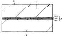
The NROM structure is the structure that the gate insulating film 2a of the MOS transistor npn npn that will form on the interarea of Semiconductor substrate 1 replaces with the ONO membrane structure of dielectric film 2a1,2a2,2a3 (for example silicon oxide film, silicon nitride film and silicon oxide film), write fashionable use channel hot electron and inject (CHE), use hot hole injection mode (BTBT:band-to-band tunneling) when wiping based on the interband tunnelling.
On gate insulating film 2a, form gate electrode 3.Gate electrode 3 is for example formed by polysilicon film, and layer forms silicide layer 4 thereon.Be formed with sidewall spacers 5 in the side of gate electrode 3.In addition, in the interarea of Semiconductor substrate 1, be formed with diffusion layer 6,7 in the short direction both sides of gate electrode 3.Upper strata at this diffusion layer 6,7 is formed with silicide layer 4.The formation technology of this NROM structure is simple, therefore be suitable for miniaturization and with the loading in mixture of logical circuit.
As other be suitable for logic with the structure that circuit loads in mixture, enumerate to have and select with MOS transistor npn npn and storage splitting bar polar form memory cell with the MOS transistor npn npn.In this structure, can adopt the higher source side of injection efficiency to inject (SSI:Source Side Injection) mode, therefore can seek to write the reduction of high speed and power supply unit area, can constitute memory cell selecting transistor and the transistor that is attached thereto with the less low-voltage transistorlike of element area, therefore can reduce the area of peripheral circuit, therefore be suitable for loading in mixture purposes.
Particularly, comprise the structure of utilizing autoregistration to come to form the MOS transistor npn npn of a side with sidewall as the splitting bar electrode structure that is suitable for miniaturization.At this moment, do not need the position alignment tolerance limit of photoetching, the transistorized grid length that forms by autoregistration can be below the minimum exploring degree of the photoetching size, therefore compares with form 2 kinds of transistorized structures respectively with photoresist, can realize finer memory cell.Wherein, for example in the TOHKEMY 2004-186452 communique (Japanese Patent Application 2002-352040 number, patent documentation 2) the disclosed memory cell that forms self-aligning grid one side with the MONOS structure be applicable to and the loading in mixture of high speed logic circuit.Fig. 2 is the memory cell that the inventor studies, and illustrating self-aligning grid one side-draw is the cutaway view of the memory cell of MONOS structure.
On the interarea of Semiconductor substrate 1, the transistor of selection and memory transistor are arranged with adjacent state configuration.The selection transistor has gate insulating film 2b that forms and the selection gate electrode 10A that forms thereon on the interarea of Semiconductor substrate 1.Gate insulating film 2b is formed by the monomer film of oxide-film, selects gate electrode 10A to be formed by polysilicon film.
In this sidewall one side of selecting gate electrode 10A, on the interarea of Semiconductor substrate 1, be formed with the memory gate electrode 11 of side wall construction across gate insulating film 2a.Memory gate electrode 11 is formed by polysilicon film.
Such memory cell structurally at first form to be selected gate electrode 10A one side, therefore can be preferably under the state in the quality at Semiconductor substrate interface, and form and select the transistor and the transistorized gate insulating film of the logical circuit portion of formation simultaneously.Elder generation makes the high speed of interface quality sensitivity is started building with the transistor of film grid, and therefore the transistor of the logical circuit portion that loads in mixture and the transistorized performance of selection improve.Can only carry out reading of canned data with the transistorized work of high performance selection, the transistor that is attached thereto also can all be made of the therefore high speed that can seek to read and the reduction of circuit area the low withstand voltage class of film.
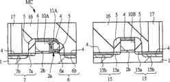
Fig. 3 illustrates the memory array structure that has used above-mentioned splitting bar polar form MONOS memory cell.Each memory cell MC has memory gate electrode 11A and selects gate electrode 10A, is configured to the shared adjacent with it diffusion layer 6 of each memory gate electrode 11A (below be also referred to as source electrode line SL (SL1, SL2)) of memory cell MC adjacent one another are.
Above-mentioned source electrode line SL forms with the state that extends abreast with word line CG (CG1, CG2), MG (MG1, MG2).Word line CG is electrically connected with a plurality of selection gate electrode 10A, and word line MG is electrically connected with a plurality of memory gate electrode 11A.Be connected electrically on the diffusion layer 7 adjacent (below be also referred to as drain electrode) with the bit line BL (BL1, BL2) of these word lines CG, MG quadrature with the selection gate electrode 10A of each memory cell MC.
Fig. 4 illustrates the layout vertical view of the memory array structure of Fig. 3.In storage array, have at the upper and lower of Fig. 4 upwardly extending many word line CG, MG every desired arranged spaced along the left and right directions of Fig. 4.Word line CG, MG are configured with state adjacent one another are.Memory cell MC forms in the zone with dotted line.Shadow representation element separated part 12.
Then, according to the work of the memory of Fig. 5~Fig. 7 key diagram 3.Typical voltage conditions when Fig. 5 illustrates memory operation.Fig. 6 illustrates the cutaway view of the memory cell when writing work, and Fig. 7 illustrates the cutaway view of the memory cell when wiping work.
Write such as shown in Figure 5 and Figure 6, utilize source side injection mode (SSI mode), select the grid weak inversion under memory gate electrode 11A and source electrode line SL for example apply the state about 9V, 5V, making respectively, utilization makes it to produce hot electron at the stronger electric field of selecting to produce between gate electrode 10A and the memory gate electrode 11A, and is injected into the gate insulating film 2a (ONO film) of memory transistor.
Wipe as Fig. 5 and as shown in Figure 7, use hot hole injection mode (BTBT mode) based on the interband tunnelling.For example apply at memory gate electrode 11A-voltage of 6V, apply for example voltage that becomes anti-phase bias voltage about 6V at source electrode line SL, utilize produce in the end of the diffusion layer 6 of source side make it to produce hot hole than highfield based on the interband tunnelling, and be injected into the gate insulating film 2a (ONO film) of memory transistor.
When the information that writes is read, apply for example 0V at memory gate electrode 11A, selecting gate electrode 10A to apply for example 1.5V, apply for example 1V in drain electrode, judge according to the size of the electric current that flows through in drain electrode.
In addition, as the method for deleting of splitting bar polar form MONOS memory, except that above-mentioned BTBT mode, for example applying in memory gate electrode in addition, the high positive voltage about 15V comes from the method for whole extraction electronics.Owing to be the mode of extracting electronics in the memory gate electrode side out, so membrane structure is MNOS structure or the thin MONOS structure of top layer oxide-film that does not have the top layer oxide-film.Whole extraction mode needs high voltage, and be difficult to extract out the electronics between memory gate electrode 11A and the adjacent selection gate electrode 10A, therefore for example in the TOHKEMY 2004-111749 communique (patent documentation 3) disclosed like that, have at sidewall and form the situation that electric field is controlled in taper.In addition, as controlling the mode of electric field and also have No. 6940757 (patent documentation 4) disclosed method of United States Patent (USP) from underlying oxide film side iunjected charge by forming taper, but there is problem, exists the division grid mode of memory cell structure, memory array structure and standard to have more different, as to be difficult to high speed problem in addition the bigger underlying oxide film deterioration of properties influence.
The manufacturing process of splitting bar polar form MONOS memory cell and standard CMOS process compatible good is suitable for loading in mixture to microcomputer etc.Fig. 8~Figure 16 illustrates the splitting bar polar form MONOS memory cell that loads in mixture inventor research and the production process of semiconductor device flow process of CMOS logic processor.What storage area (storage array) was represented in the left side of each figure wants portion's section, the right side represent to form CMOS logic region want portion's section.
Fig. 8 is the stage of the gate material 10 that forms the gate insulating film 2b that is made of silicon oxide film on the interarea of the Semiconductor substrate 1 that is made of monocrystalline silicon (Si), be made of polysilicon film.The transistor common grid dielectric film 2b of the selection transistor of storage area and logic section.Though omit in the drawings, form component isolation structure as this last stage use usual way.
Fig. 9 is the stage that then forms the transistorized gate electrode 10A of selection of storage area by photoetching and dry etching.In this stage, the gate material 10 of logic region is not carried out graphically.
Then, Figure 10 is deposit SiO
2Film, Si
3N
4Film, SiO
2The stage of the ONO film of the 3-tier architecture of film (gate insulating film 2a).Then, Figure 11 is in order to form the memory gate electrode material, as the mixed amorphous silicon of impurity of the second electrode material deposit, it is carried out only forming as the residual amorphous silicon film of sidewall in the two side of selecting gate electrode 10A after the etching stage of memory gate electrode 11A with dry etching.Then, Figure 12 removes the unwanted memory gate electrode 11A of a side among the memory gate electrode 11A of the two side of selecting gate electrode 10A by dry etching, further by removing the gate insulating film 2a of its lower floor, only come to form memory gate electrode 11A at the sidewall of a side of selecting gate electrode 10A.
Then, the gate material 10 of logic region is carried out graphically, come to form gate electrode 10B at logic region as shown in Figure 13 by using photoetching and dry etching.Then,, form n type diffusion layer 6a, the 7a of low impurity concentration,, form diffusion layer 15a, the 15a of low impurity concentration by importing impurity at logic region by importing impurity at storage area.Then, on the interarea of Semiconductor substrate 1 deposit by SiO
2After the dielectric film that forms,, as shown in Figure 14, form sidewall 5 at the sidewall of the gate electrode 10B of selection gate electrode 10A, the memory gate electrode 11A of storage area and logic region by it is carried out etching.Then,, form n type diffusion layer 6b, the 7b of high impurity concentration, form source electrode, drain electrode diffusion layer 6,7 by importing impurity at storage area.In addition,, form diffusion layer 15b, the 15b of high impurity concentration, form source electrode, drain electrode diffusion layer 15 by importing impurity at logic region.
Then, as shown in Figure 15, selecting gate electrode 10A, gate electrode 10B, memory gate electrode 11A and diffusion layer 6b, 7b, formation for example is made of cobalt silicide above the 15b silicide layer 4, the low resistanceization of seeking each several part.Then, as shown in Figure 16, in deposit on the interarea of Semiconductor substrate 1 behind the dielectric film 16 of ground floor, make its upper surface planarization, form contact hole 17.Then, through about 3~6 layers metal line formation operation of standard, but its explanation is omitted.
, the inventor find NROM structure as described above MONOS memory cell, splitting bar electrode structure the MONOS memory cell all be suitable for miniaturization, with standard CMOS process compatible good in, have following problem.
The first, can list owing in the work of wiping, using hot hole injection mode (BTBT mode) to make the current sinking when wiping become big example easily based on the interband tunnelling.With Fig. 7 is example, diffusion layer 6 and memory gate electrode 11 apply respectively 6V for example and-voltage of 6V, the part in the hole that is produced by the interband tunnelling is accelerated and injects to the memory gate electrode direction, but major part flows to Semiconductor substrate 1 and becomes useless electric current.Its value reaches several μ A/ unit unexpectedly, though simultaneously also with to wipe bit number relevant, constitute the reason that needs large-scale power supply in order to wipe.In addition, the erasing voltage increase that writes electrical level rising, is used to improve erasing speed that is used to improve charge-retention property also makes and wipes electric current and increase.Therefore, the high performance of system also can cause the maximization of the charge pump circuit of power supply, and the circuit area of memory module increases.
The second, have owing to from the more problem that causes anti-interference difference of the leakage current of diffused junction.The writing of NROM structure, splitting bar electrode structure MONOS all used respectively the holoe carrier based on CHE or SSI.When injecting wherein, become the jamming pattern that mistake writes from the leakage current mixing of diffused junction.The mitigation of diffused junction is effective to reducing leakage current, but need spread and become to a certain degree precipitous in order to make it to take place the interband tunnelling, takes into account as long as use wiping of BTBT mode just to be difficult to the two.The result is in order to remedy the deficiency of anti-interference, need to adopt with storage array cut apart unit design more carefully shorten interference time countermeasure, the circuit area of memory module increases.
The purpose of this invention is to provide and a kind ofly can in semiconductor device, dwindle the technology of the area of nonvolatile storage with the non-volatile memory cells that in gate insulating film, contains charge storage portion.
Above-mentioned and other purposes of the present invention and new feature are come clear and definite according to the record and the accompanying drawing of this specification.
The summary of representative art scheme is as follows in the disclosed invention of simple declaration the application.
Promptly, the present invention is in the semiconductor device with the non-volatile memory cells that contains charge storage portion in gate insulating film, by the change section of local physical form is set on the gate electrode on the above-mentioned gate insulating film, apply suitable current potential in this change section, so that by the FN tunnelling from above-mentioned gate electrode to above-mentioned charge storage portion iunjected charge, obliterated data.
The effect that is obtained by the representative art scheme in the disclosed invention of simple declaration the application is as follows.
Promptly, in semiconductor device with the non-volatile memory cells that in gate insulating film, contains charge storage portion, by the change section of local physical form is set on the gate electrode on the above-mentioned gate insulating film, apply suitable current potential in this change section, so that by the FN tunnelling from above-mentioned gate electrode to above-mentioned charge storage portion iunjected charge, obliterated data, thereby can make the electric current that when wiping work, flows through be reduced to insignificant degree, and because its characteristic does not rely on diffused junction, so can relax diffused junction, therefore can dwindle the area of nonvolatile storage.
Description of drawings
Fig. 1 is the cutaway view of the NROM that studies of the inventor.
Fig. 2 is the memory cell that the inventor studies, and is to be the cutaway view of the memory cell of MONOS structure with self-aligning grid one side-draw.
Fig. 3 has been to use the circuit diagram of the memory array structure of splitting bar polar form MONOS memory cell.
Fig. 4 is the layout vertical view of the memory array structure of Fig. 3.
The key diagram of the exemplary voltages condition when Fig. 5 is the work of memory of Fig. 3.
Fig. 6 be Fig. 3 memory write work the time the cutaway view of memory cell.
Fig. 7 be Fig. 3 memory wipe work the time the cutaway view of memory cell.
Fig. 8 loads in mixture to want portion's cutaway view in the semiconductor device manufacturing step of the splitting bar polar form MONOS memory cell of inventor research and CMOS logic processor.
Fig. 9 wants portion's cutaway view in the manufacturing step of the then semiconductor device of Fig. 8.
Figure 10 wants portion's cutaway view in the semiconductor device manufacturing step of then Fig. 9.
Figure 11 wants portion's cutaway view in the semiconductor device manufacturing step of then Figure 10.
Figure 12 wants portion's cutaway view in the semiconductor device manufacturing step of then Figure 11.
Figure 13 wants portion's cutaway view in the semiconductor device manufacturing step of then Figure 12.
Figure 14 wants portion's cutaway view in the semiconductor device manufacturing step of then Figure 13.
Figure 15 wants portion's cutaway view in the semiconductor device manufacturing step of then Figure 14.
Figure 16 wants portion's cutaway view in the semiconductor device manufacturing step of then Figure 15.
Figure 17 wants portion's cutaway view in the semiconductor device manufacturing step of one embodiment of the present invention.
Figure 18 wants portion's cutaway view in the semiconductor device manufacturing step of then Figure 17.
Figure 19 wants portion's cutaway view in the semiconductor device manufacturing step of then Figure 18.
Figure 20 wants portion's cutaway view in the semiconductor device manufacturing step of then Figure 19.
Figure 21 wants portion's cutaway view in the semiconductor device manufacturing step of then Figure 20.
Figure 22 wants portion's cutaway view in the semiconductor device manufacturing step of then Figure 21.
The Semiconductor substrate of the operating state when Figure 23 is the reading of semiconductor device of expression one embodiment of the present invention want portion's cutaway view.
Figure 24 be expression one embodiment of the present invention semiconductor device the Semiconductor substrate of writing fashionable operating state want portion's cutaway view.
The Semiconductor substrate of the operating state when Figure 25 is the wiping of semiconductor device of expression one embodiment of the present invention want portion's cutaway view.
Figure 26 is the curve chart of the relation of expression electric field and FN tunnelling current.
Figure 27 is the erasing characteristic (threshold voltage-erasing time) of semiconductor device is measured storage grid voltage in expression as parameter result's a curve chart.
Figure 28 gathers the reading of the semiconductor device of representing one embodiment of the present invention, writes the key diagram with the voltage of erase status.
Figure 29 is the cutaway view of memory cell of the semiconductor device of other execution modes of the present invention (execution mode 2).
Figure 30 gathers the reading of the semiconductor device of representing execution mode 2, writes the key diagram with the voltage of erase status.
Figure 31 is the cutaway view of the memory cell in the semiconductor device manufacturing step of other execution modes of the present invention (execution mode 3).
Figure 32 is the cutaway view of the memory cell in the semiconductor device manufacturing step of then Figure 31.
Figure 33 is the cutaway view of memory cell of the semiconductor device of other execution modes of the present invention (execution mode 4).
Figure 34 is the cutaway view of the memory cell in the semiconductor device manufacturing step of other execution modes of the present invention (execution mode 5).
Figure 35 is the cutaway view of the memory cell in the semiconductor device manufacturing step of then Figure 34.
Figure 36 is the cutaway view of the memory cell in the semiconductor device manufacturing step of other execution modes of the present invention (execution mode 6).
Figure 37 is the cutaway view of the memory cell in the semiconductor device manufacturing step of then Figure 36.
Figure 38 is the cutaway view of the memory cell in the semiconductor device manufacturing step of then Figure 37.
Figure 39 is the cutaway view of the memory cell in the semiconductor device manufacturing step of other execution modes of the present invention (execution mode 7).
Figure 40 is the cutaway view of the memory cell in the semiconductor device manufacturing step of then Figure 39.
Figure 41 is the cutaway view of the memory cell in the semiconductor device manufacturing step of then Figure 40.
Figure 42 be expression execution mode 7 semiconductor device the Semiconductor substrate of writing fashionable operating state want portion's cutaway view.
The Semiconductor substrate of the operating state when Figure 43 is the wiping of semiconductor device of expression execution mode 7 want portion's cutaway view.
Figure 44 is the cutaway view of memory cell of the semiconductor device of other execution modes of the present invention (execution mode 10).
Figure 45 is the cutaway view of memory cell of the semiconductor device of other execution modes of the present invention (execution mode 11).
Figure 46 is the reading of semiconductor device of gathering expression other execution modes of the present invention (execution mode 12), write the key diagram with the voltage of erase status.
Figure 47 is the reading of semiconductor device of gathering expression other execution modes of the present invention (execution mode 15), write the key diagram with the voltage of erase status.
Figure 48 is the circuit diagram of structure example of storage array of the semiconductor device of expression inventor research.
Figure 49 is the circuit diagram of structure example of storage array of the semiconductor device of expression one embodiment of the present invention.
Embodiment
The problems referred to above are owing to the hot hole injection mode of using in the work of wiping based on the interband tunnelling (BTBT mode).In order to address the above problem, replace to that to wipe electric current less and do not need the erase mode of precipitous diffused junction to get final product.
The method of using the work of FN tunnelling when wiping is arranged as solution.If adopt FN tunnelling mode, the electric current that then flows through when wiping work can be reduced to insignificant degree, and because its characteristic does not rely on diffused junction, so can relax diffused junction.On the other hand, in order to cause the work of FN tunnelling, need high electric field,, need the such high voltage of 15~20V when when planar film structure and charge-retention property are considered necessary thickness.Instead this might increase the power circuit area.For low-voltage also can cause the work of FN tunnelling, utilize the shape of concentrating the character of electric field to form the high electric field of generation with the change section of local physical form to get final product.Can use structure and the manufacturing process that forms protuberance at gate electrode as its method.
Particularly, at first under the situation of splitting bar electrode structure, utilize the bight of memory gate electrode.When suitable current potential is provided in the close angle part of memory gate electrode and the dielectric film of adjacent control grid electrode, can be by FN tunnelling iunjected charge.For the injection rate that increases electric charge also can form acute angle with above-mentioned bight.The electric charge of the opposite polarity of the electric charge that counteracting is injected in above-mentioned bight injects and uses source side injection (SSI) to get final product.Therefore, can realize writing and wiping work.
Under the situation of NROM structure, the side of oxidation memory gate electrode unevenly forms acute angle with the bight of memory gate electrode, thereby can cause the work of FN tunnelling.
The relation that the acute angle formation technology in the bight of memory gate electrode and electric charge inject required current potential has a plurality of choice of technology items, below describes possible combination and effect.
In addition, in the following embodiments, be divided into a plurality of execution modes for convenience of explanation as required and describe, but except situation about expressing especially, there are relation in part or all variation of an execution mode and other execution modes, details, supplementary notes etc.In addition, at the institute's drawings attached that is used for illustrating present embodiment, have the identical symbol of parts mark of identical function, its repeat specification is omitted as far as possible.Below describe embodiments of the present invention with reference to the accompanying drawings in detail
[execution mode 1]
The semiconductor device of embodiment of the present invention 1 for example is the logical operation circuit of representative and the semiconductor device of non-volatile memory with the microcomputer for having on semi-conductive substrate.The memory cell of the non-volatile memory of the semiconductor device of present embodiment 1 (non-volatile memory cells) is the MONOS memory of autoregistration splitting bar electrode structure.The basic structure of memory cell is as above-mentioned Fig. 2 waits explanation.Memory array organization is as illustrating at Fig. 3, and the layout of memory cell MC is as illustrating at Fig. 4.The part that dotted line surrounded among Fig. 4 is equivalent to a memory cell MC.Memory cell MC adjacent one another are each other selection gate electrode 10A and the configuration of memory gate electrode 11A be generally left-right symmetric.Though be above-mentioned term, memory gate electrode is instigated the film (ONO film, charge storage portion) of the catching electric charge gate electrode for the MOS transistor of dielectric film and the side that keeps here.Performance is to the gate electrode of the MOS transistor of a side of the effect of its selection when in addition, selecting gate electrode to refer to read.
The manufacture method of the semiconductor device of present embodiment at first, is described according to Figure 17~Figure 22.Figure 17~Figure 22 illustrates and wants portion's cutaway view in the semiconductor device manufacturing step of present embodiment.In Figure 17~Figure 22, what the left side illustrated storage area (storage array) wants portion's section, and what the right side illustrated the logic region that forms CMOS (Complementary MOS) wants portion's section.Therefore the manufacture method of the semiconductor device of present embodiment is main describing with the different piece so that the semiconductor device manufacturing process that illustrates with above-mentioned Fig. 8~Figure 16 is a benchmark.In the manufacturing of semiconductor device, adopt for example process rule of 90nm node.
As shown in figure 17, use usual way after having formed the such element separated part 12 of ditch type separated part for example on the interarea of Semiconductor substrate 1, in the Semiconductor substrate 1 that for example forms by p type monocrystalline silicon (Si), for example inject at the Qn of nMOS portion ion that p type boron impurities (B) forms p type trap PW, for example injecting at the Qp of pMOS portion and storage area ion, n type foreign matter of phosphor (P) forms n type trap NW.Then, the channel ion of the high withstand voltage MOS portion that carries out thick film inject and grid oxidation film formation after, also carry out the threshold voltage adjustment of logic region and storage area and inject with channel ion.
Then, as shown in figure 18, for example with 800 ℃ of heat oxide films that become the transistorized public grid dielectric film 2b that selects transistor and logic region that form thickness 2nm, the gate material 10 that for example constitutes of deposition thickness 220nm by polysilicon film.The film forming of this gate material 10 for example free from admixture doping is carried out for 640 ℃ with film-forming temperature.Then inject the doping impurity of carrying out, for example partly inject 1 * 10 at the gate electrode of the Qp of pMOS portion respectively to gate material 10 by ion
15Atoms/cm
2Boron (B), for example inject 6 * 10 at the Qn of nMOS portion
15Atoms/cm
2Phosphorus (P), separately make p
+Type gate electrode portion and n
+Type gate electrode portion.The transistorized gate electrode part of selection that becomes storage area is injected for example boron with the condition identical with the Qp of pMOS portion, to become p
+The type gate electrode.
Then, gate material 10 is carried out graphically, as shown in figure 19, form the figure of gate electrode 10A, 10Bn, 10Bp by using photoetching and dry etching.Then, with Semiconductor substrate 1 sacrificial oxidation for example after the 3nm, inject, inject for example boron (BF on the top layer of Semiconductor substrate 1 as only being used for that storage area is carried out the counter ion that the threshold voltage of memory transistor adjusts
2+).
Then, as shown in figure 20, as the deposit of charge storage portion for example by SiO
2Film/Si
3N
4Film/SiO
2The gate insulating film 2a of 3 layers of formation of film (thickness is respectively for example 4nm/8nm/5nm) (ONO film, storage grid dielectric film).The SiO of gate insulating film 2a
2Film for example all uses ISSG oxidizing process (In Situ Steam Generation) with 900 ℃ of film forming in substrate side and gate electrode side.At this moment, at the SiO of Semiconductor substrate 1 side
2After film forms, also for example handle and carry out interface enhancing by nitric oxide (NO).The Si of gate insulating film 2a
3N
4Film is by CVD (Chemical Vapor Deposition) method film forming.
Herein, the above-mentioned dielectric film 2a2 among the gate insulating film 2a is the main charge storage portion of main stored charge.Herein, the constituent material of dielectric film 2a2 is Si
3N
4Film (silicon nitride film), but Si
3N
4The stoichiometric proportion of film depends on membrance casting condition, therefore expresses and imprecision, even be expressed as Si
3N
4Under the situation of film, also comprise being expressed as Si
xN
ySituation.As the charge-trapping film, can be various materials, but from the compatibility of semiconductor technology, use Si as standard
3N
4Film.
Then, on gate insulating film 2a, mixed after the amorphous silicon film of impurity as the second electrode material deposit in order to become the memory gate electrode material, by it being carried out etching with the anisotropic dry etching, as shown in Figure 20, respectively in the two side of selecting gate electrode 10A and gate electrode 10Bn, 10Bp with the residual amorphous silicon film of sidewall shape, form memory gate electrode 11A.The impurity of memory gate electrode 11A is for for example mixing 4 * 10
20Atoms/cm
3Above phosphorus becomes n
+The type gate electrode.
Then, use photoetching and dry etching, such as shown in figure 21, in storage area, remove the unwanted memory gate electrode 11A that selects gate electrode 10A one side.In logic region, remove the unwanted memory gate electrode 11A of gate electrode 10Bn, 10Bp both sides.And then remove the remaining gate insulating film 2a (ONO film) that exposes by dry etching and wet etching.On memory gate electrode 11A, form bight (angle) 11cn with gate insulating film 2a in a side (side adjacent) adjacent with selecting gate electrode 10A.
Then, form epi region, therefore inject for example 7keV, 6 * 10 at the storage area ion
13Atoms/cm
2Boron (BF
2+), inject for example 5keV, 1 * 10 at the pMOS of the logic region Qp of portion ion
14Atoms/cm
2Boron (BF
2+), inject for example 5keV, 6 * 10 at the nMOS of the logic region Qn of portion ion
14Atoms/cm
2Arsenic (As).In storage area,, make the impurity dose of impurity dose less than the logic region side in order to protect memory gate electrode 11A and to prevent to penetrate from the impurity of side wall ends.
Thus, such as shown in figure 22, form n type diffusion layer 6a, the 7a of extension at storage area with low impurity concentration, form extension with low impurity concentration diffusion layer 15na, 15na at the nMOS of the logic region Qn of portion, form extension low impurity concentration diffusion layer 15pa, 15pa at the pMOS of the logic region Qp of portion.
Then, on the interarea of Semiconductor substrate 1 deposit by SiO
2After the dielectric film that forms, by it is carried out etching, form sidewall 5 at the sidewall of gate electrode 10Bn, the 10Bp of gate electrode 10A, the 11A of storage area, logic region.
Then, in order to form high concentration diffusion layer, at the pMOS of storage area and the logic region Qp of portion all for example with 15keV, 1 * 10
13Atoms/cm
2Condition inject boron (B
+).Further, in logic region, for example with 20keV, 2 * 10
15Atoms/cm
2Condition inject boron (BF
2+), in storage area, for example with 15keV, 1 * 10
15Atoms/cm
2Condition inject boron (BF
2+).In storage area,, make the injection energy of impurity and dosage injection energy and dosage less than the impurity of logic region side in order to protect memory gate electrode 11A and prevent to penetrate from the impurity of side wall ends.Thus, at n type diffusion layer 6b, the 7b of storage area formation high impurity concentration, form source electrode, drain electrode diffusion layer 6,7.In addition, diffusion layer 15pb, 15pb in that the pMOS of the logic region Qp of portion forms high impurity concentration form source electrode, drain electrode diffusion layer 15p.
In addition, at the nMOS of the logic region Qn of portion for example with 50keV, 2 * 10
15Atoms/cm
2Condition inject arsenic element, for example with 40keV, 1 * 10
13Atoms/cm
2Condition inject phosphorus.Thus, diffusion layer 15nb, 15nb in that the nMOS of the logic region Qn of portion forms high impurity concentration form source electrode, drain electrode diffusion layer 15n.
When forming above-mentioned extension and high concentration diffusion layer, the ion implanting conditions that changes the Qp of pMOS portion of storage area and logic region respectively causes step to increase.But, consider in order to make the n of memory gate electrode 11A
+The type gate electrode can not carry out extension that ion injects and the p type impurity polarity of high concentration diffusion layer is reversed because of autoregistration thereon ground, should be noted that the injection condition that relaxes injection energy and dosage.At this, finished the basic structure of storage area.This following situation about illustrating with the above-mentioned Figure 15 of use and Figure 16 similarly carries out coming via heat treatment, suicided the standard technology of the wiring step (form dielectric film, form contact site, form wiring material) of 3~6 layers of repetitions.In addition, between above-mentioned steps, insert cleaning step at any time or detect step with normally used method.
The method of work of non-volatile memory cells MC of the semiconductor device of the present embodiment that has charge storage portion in gate insulating film then, is described.
The conduction type as the charge carrier of MOS transistor of the memory cell of present embodiment uses the pMOS opposite with nMOS.Figure 23 illustrates the operating state when reading.Because be the pMOS type, therefore when basically Semiconductor substrate 1 and source electrode (diffusion layer 6) being taken as same potential and when gate electrode applies negative voltage, flowing through the conducting electric current.Different therewith at this, in the following way: apply for example supply voltage of 1.5V in Semiconductor substrate 1 and source electrode (diffusion layer 6), select gate electrode 10A and memory gate electrode 11A under the situation of for example 0V of negative direction, to flow through the conducting electric current.This is in order similarly not use negative voltage with logic region and to control.When injecting electronics or hole, the threshold voltage variation of memory transistor side is carried out non-volatile information stores at the dielectric film 2a2 of the gate insulating film 2a of this memory cell MC (ONO) (silicon nitride film, main charge storage portion).
The condition of the judgement of the cut-off state when reading be memory cell MC whether be below the certain value by leakage current, inject the hole that threshold voltage becomes the following degree of benchmark.The condition of the judgement of conducting state is whether to flow through certain above conducting electric current on the contrary, injects the electronics of required amount.The absolute value of conducting electric current is by reading the operating frequency decision, if the work about for example common 20MHz for example can be 5 μ A/bit.For example, when reading, for example require 10~30 μ A/bit with 50~80MHz at a high speed.The transistor of memory cell MC is that the manner of pMOS type is compared in the mode that same size obtains the nMOS type of double read current with use, bad aspect the conducting electric current on the principle, but owing to be that storage grid length extremely shortens to for example less side wall grid of 50nm left and right sides channel resistance, electronics is easy to inject than the hole and therefore can promotes threshold voltage (direction that increases at the electric current of pMOS) biglyyer, owing to above reason etc., can obtain for example current value about 20 μ A/bit, be suitable for most of purposes.
Figure 24 illustrates and writes fashionable operating state.In writing, use source side same as described above to inject (SSI), but be not electronics but the hole is injected into gate insulating film 2a (being mainly dielectric film 2a2).Memory gate electrode 11A is for example being applied-9V, to source electrode (diffusion layer 6) for example apply-state of 5V under, respectively select gate electrode 10A and drain electrode (diffusion layer 7) for example apply-1V and-0.5V comes selecting to produce the weak inversion state under the gate electrode 10A, inverted status portion under memory gate electrode 11A produces source voltage, utilization and this source voltage between the high electric field that produces produce hot hole, utilize the bigger negative voltage of memory gate electrode 11A, can gate insulating film 2a (the ONO film be mainly dielectric film 2a2 (silicon nitride film, main charge storage portion)) injected hole efficiently.Inject with the hole of passing through the interband tunnelling of using in the above-mentioned research example and to compare, the injection efficiency of SSI is higher, even therefore under the situation of identical injected hole, also can reduce the damage that brings to gate insulating film 2a (ONO film).Here, will inject and state that the absolute value of threshold voltage descends is defined as the write state of this memory cell MC by the hole.Whether each memory cell MC is write, can be controlled at the electric current of selecting to flow through under the gate electrode 10A by the size that utilization is connected to the drain voltage of bit line and determine.
Figure 25 illustrates the operating state when wiping.Work when wiping only for example applies at memory gate electrode 11A-negative voltage of 11V, and another terminal is for example 0V or open circuit (OPEN).,, source electrode (diffusion layer 6) and drain electrode (diffusion layer 7) are taken as for example open circuit herein, will select gate electrode 10A and Semiconductor substrate 1 to be taken as for example 0V (ground connection) according to the situation on the circuit.Potential difference by memory gate electrode 11A and Semiconductor substrate 1 for example is 8MV/cm at the electric field that gate insulating film 2a (ONO film) " fifty-fifty " produces.Though should value anything but little, in the erasing time, being inadequate by FN tunnelling work iunjected charge.But, in memory gate electrode 11A, be formed near among the side of the gate insulating film 2a of the side of selecting gate electrode 10A and the bight 11cn near the part of the hand-deliver fork of the gate insulating film 2a on the interarea of Semiconductor substrate 1, equipotential plane sharply changes, therefore the electric field concentration of local for example obtains the above electric field of the needed 10MV/cm of high speed FN tunnelling work.Therefore, inject electronics from the bight 11cn of memory gate electrode 11A to the dielectric film 2a2 of gate insulating film 2a (ONO film) (main charge storage portion), the absolute value of threshold voltage rises, and wipes work.
At this, Figure 26 illustrates the relation of electric field and FN tunnelling current.The FN tunnelling current is with J=AE
2Exp (B/E) (E: electric field, A, B: expression constant), be index with respect to electric field and change, therefore sharply rise.Therefore, as noted above such, the electric charge under the 8MV/cm injects insufficient, just can cause substantial injection more than the 10MV/cm.At this, when the par at gate insulating film 2a (ONO film) produces electric field more than the 11MV/cm fifty-fifty, will produce superfluous electric charge and inject, therefore the above electric field of preferred 11MV/cm at whole.Inject effect for the internal field that obtains present embodiment concentrates the electric charge that brings, it is above and be below the 11MV/cm to be preferably designed for electric field value average out to 7MV/cm that the potential difference of utilizing memory gate electrode 11A and Semiconductor substrate 1 produces in the par of gate insulating film 2a (ONO film).At this moment, when suppressing whole injection, take place to concentrate the electric charge that causes to inject by internal field.
It is the result of the erasing characteristic (threshold voltage-erasing time) of this device of parameter measurement that Figure 27 illustrates with storage grid voltage.Source voltage Vs=selects grid voltage Vcg=drain voltage Vd=underlayer voltage Vsub=0V.
Structurally, the memory cell MC on the identical word line of the shared memory gate electrode 11A that applies negative voltage is all wiped simultaneously, but because flash memory is wiped together, therefore is not suitable for.And, since the FN tunnelling to wipe electric current almost nil, the memory gate electrode 11A that wipes on the module all can be wiped simultaneously.
Figure 28 gathers the voltage of above reading, writing with erase status is shown.Figure 28 is taken as power source voltage Vcc and the situation of not using negative voltage to read by the current potential with Semiconductor substrate 1, and in addition, memory gate electrode 11A is the situation that is taken as the biasing hold mode.
[execution mode 2]
As the variation of above-mentioned execution mode 1, the semiconductor device of present embodiment 2 is described according to Figure 29.Figure 29 is the cutaway view of memory cell MC of the semiconductor device of present embodiment 2.In addition, for clear and definite difference, Figure 30 illustrates operating voltage.Figure 30 is taken as power source voltage Vcc and the situation of not using negative voltage to read by the current potential with Semiconductor substrate 1, and in addition, memory gate electrode 11A is the situation that is taken as the hold mode of do not setover (Vmg=Vsub).
Be applied to the supply voltage that voltage on the memory gate electrode 11A for example is set at the 1.5V identical with Semiconductor substrate 1 when reading.With the difference of the above-mentioned execution mode 1 storage grid voltage Vmg when reading only, identical by it is taken as with substrate side voltage, can deduct the electric field (electrode potential-substrate electric potential) that produces among the gate insulating film 2a (ONO film) of the memory when reading and become zero.The electric charge that this result can suppress to be caused by electric field is escaped, and improves charge-retention property.Shortcoming is that the threshold voltage of memory cell MC is further risen.Therefore, need to allow the reduction of subthreshold value characteristic to increase counting channel ion injection rate, or allow negative electrical charge increase to anti-rewriting to increase ion injection rate when wiping.No matter get which kind of countermeasure, can both carry out suitable design according to the target mode.
[execution mode 3]
At first, through with the identical manufacturing process of step with Figure 17~Figure 19 explanation of above-mentioned execution mode 1.This stage forms selection gate electrode 10A across gate insulating film 2b on the interarea of Semiconductor substrate 1.
Then,, such as shown in figure 31 by for example in present embodiment 3 with 800 ℃ of wet oxidations that carry out 6nm, the side of selecting gate electrode 10A, above and the interarea of Semiconductor substrate 1 form dielectric film 20a, 20b, the 20c that constitutes by silica.At this moment, in the high selection gate electrode 10A of impurity concentration, side wall centers portion is by many especially oxidations, and select gate electrode 10A end (especially bottom) stress influence and suppress oxidation rate.Like this, because of impurity concentration and stress produce difference on oxidation rate, the result selects the dielectric film 20a of gate electrode 10A to become spindle shape.
Then, after the dielectric film 20c of the interarea of removing Semiconductor substrate 1, with above-mentioned execution mode 1 in the same manner, steps such as the counter ion of adjusting via the threshold voltage that is used for storage part injects, the removing of the amorphous silicon film deposit of the film forming of gate insulating film 2a (ONO film), impurity and etching, residue gate insulating film 2a (ONO film), extension formation, the formation of oxide-film sidewall, high concentration diffusion layer formation, suicided etc. form memory cell MC shown in Figure 32.
In present embodiment 3, because the dielectric film 20a that forms spindle shape in the side of selecting gate electrode 10A, the bight 11cn of memory gate electrode 11A (in memory gate electrode 11A, near the side of the gate insulating film 2a of the side of selecting gate electrode 10A and the bight that forms near the part of the hand-deliver fork of the gate insulating film 2a on the interarea of Semiconductor substrate 1) forms more sharp-pointed acute angle (less than the acute angles of 90 degree).The result compares with the situation of above-mentioned execution mode 1 in the work of wiping, and electric field further concentrates on the bight 11cn of memory gate electrode 11A, therefore can wipe work efficiently.In the product of reality, the high speed of wiping by utilization and apply the reduction of voltage when this performance raising amount is applied to wipe is realized the raising with reliability dwindled of circuit area.
[execution mode 4]
At first, after through the manufacturing process identical, be used to form the photoetching of the selection gate electrode figure of storage area, select gate electrode 10A by dry etching processing with the step with Figure 17~Figure 19 explanation of above-mentioned execution mode 1.At this moment, compare change dry etching condition with above-mentioned execution mode 1,, make the bottom (Semiconductor substrate 1 side) of selecting gate electrode 10A become the processing of reverse tapered shapes in the final stage of gate etch step.It is as well known to those skilled in the art being used for method for processing.Particularly, in the final stage of processing, change gaseous species, temperature and condition of plasma are to become the so anisotropic condition of minimizing of sidewall deposit that reduces.
As a result, completion morphology as shown in Figure 33 is such, forms the back taper 10A1 of portion at the sidewall of selecting gate electrode 10A.That is, the bottom of selecting gate electrode 10A along with from the interarea of Semiconductor substrate 1 away from, select the width (short direction size) of gate electrode 10A to become big gradually.As a result, form more sharp-pointed acute angle (less than the acute angle part of 90 degree) across the bight 11cn of the gate insulating film 2a memory gate electrode 11A adjacent with the sidewall of selecting gate electrode 10A.
When form selecting gate electrode 10A, for also forming reverse tapered shapes simultaneously, the sidewall of the gate electrode that makes the logic region MOS transistor avoids taking place undesirable characteristic variations, hide whole logic regions with the photoetching resist.The grid of logic region is used with now opposite way thereafter and is processed with resist covering storage area.The result obtains the effect identical with above-mentioned execution mode 3.
Select the taper of the sidewall of gate electrode 10A not necessarily to need only to be formed on the bottom of selecting gate electrode 10A, also can form and select the whole sidewall of gate electrode 10A to become reverse tapered shapes.
[execution mode 5]
At first, after through the manufacturing process identical with the step with Figure 17~Figure 19 explanation of above-mentioned execution mode 1, same with explanation in the above-mentioned execution mode 1, carry out sacrificial oxidation, be used for storage part is carried out the counter ion injection of threshold voltage adjustment, the film forming of gate insulating film 2a (ONO film), then as shown in figure 34, the gate material 11 that forms by the amorphous silicon of the impurity that for example mixed of deposit.
Then, in present embodiment 5, different with above-mentioned execution mode 1, not direct etch-gate electrode material 11, form the mask of resist by photoetching, this mask is implemented dry etching as etching mask to gate material 11 handle, thus as shown in Figure 35, form the figure of memory gate electrode 11B.At this, the coupling error width of above-mentioned mask is designed to drop in the width (short direction size) of selecting gate electrode 10A, and the part of memory gate electrode 11B forms to reach the shape of selecting on the gate electrode 10A.Then, form memory cell MC via the step identical with above-mentioned execution mode 1.
The working method of memory cell MC is identical with above-mentioned execution mode 1,2.Wherein, the grid length Lg of memory gate electrode 11B can be designed under the situation of this structure long enough, therefore though the conducting electric current descends, short-channel properties improves.As a result, can suppress cut-off leakage current, characteristic deviation, therefore be suitable for device towards low-power consumption.
[execution mode 6]
The semiconductor device of present embodiment 6 also has the non-volatile memory cells MC of splitting bar electrode structure.Wherein, the situation of present embodiment 6 makes memory gate electrode and forms prior to selecting gate electrode, and, use non-self-registered technology to form in the same manner with above-mentioned execution mode 5.
At first, Semiconductor substrate 1 is for example being carried out the 3nm sacrificial oxidation with 800 ℃, carrying out after the ion injection to raceway groove, such as shown in figure 36, on the interarea of Semiconductor substrate 1, form gate insulating film 2a.Gate insulating film 2a has the structure that begins to stack gradually dielectric film 2a1,2a2,2a3 from lower floor.Dielectric film 2a1 is for example by silicon oxide film (SiO
2Film) form, its thickness for example is about 4nm.Dielectric film 2a2 is for example by silicon nitride film (Si
3N
4Film) form, its thickness for example is about 8nm.Dielectric film 2a3 is for example by silicon oxide film (SiO
2Film) form, thickness is about 5nm.
Then, the deposit memory gate electrode forms with gate material 11 on gate insulating film 2a.Gate material 11 is for example formed by polysilicon, and its thickness for example is 200nm.The film forming of gate material 11 is for example as doping impurity for example 4 * 10
20Atoms/cm
3Phosphorus, film-forming temperature for example is taken as 610 ℃ carries out.
Then, on the upper surface of gate material 11, form masked film 21.Masked film 21 is for example formed by silicon oxide film, and its thickness for example is 50nm.
Then, such as shown in figure 37 by gate material 11 being used to form the photoetching and the dry etching of memory gate electrode, form memory gate electrode 11C.Then, on the interarea of Semiconductor substrate 1 deposit for example by the film formed dielectric film of silica to cover after the memory gate electrode 11C, by it being carried out etchback (etch back), form the less sidewall spacer 22 that forms with above-mentioned dielectric film in the side of memory gate electrode 11C.
Then, for example, such as shown in figure 38 after Semiconductor substrate 1 is implemented the sacrificial oxidation processing by the thermal oxidation of 800 ℃ of enforcements, form for example by the film formed gate insulating film 2b of the silica about thickness 2nm.This gate insulating film 2b becomes the selection gridistor of storage area and the transistor institute gate common dielectric film of logic region.Then, deposit is for example after the polysilicon film about thickness 220nm on the interarea of Semiconductor substrate 1, in this polysilicon film, inject for example boron at the gate electrode formation portion ion of the PMOS of storage area and the logic region Qp of portion, inject for example phosphorus at the nMOS of the logic region Qn of portion ion.
Then, above-mentioned polysilicon film is carried out graphically, form at storage area and select gate electrode 10C, form gate electrode 10Bn, 10Bp (with reference to Figure 22) at logic region by photoetching and dry etching.Then, similarly by carrying out extension formation, the formation of oxide-film sidewall, high concentration diffusion layer formation, suicided, finish memory cell MC with above-mentioned.
The situation of present embodiment 6, by forming memory transistor earlier, the oxide-film quality of the gate insulating film 2a (ONO film) of storage area is improved, therefore can obtain following advantage: charge-retention property is improved, short-channel properties is improved owing to do not need counter ion to the groove of memory transistor to inject.The raising of short-channel properties can obtain to reduce by leakage, be suitable for the Devices Characteristics towards low-power consumption, and noiseproof feature is improved, and therefore can realize the storage array design that circuit area is less.
[execution mode 7]
The semiconductor device of present embodiment 7 is the MONOS memory of NROM structure.
At first, similarly Semiconductor substrate 1 is for example being carried out the 3nm sacrificial oxidation with 800 ℃, carrying out after the ion of raceway groove injects with above-mentioned execution mode 6, such as shown in figure 36, on the interarea of Semiconductor substrate 1, form gate insulating film 2a.Gate insulating film 2a has the structure that stacks gradually dielectric film 2a1,2a2,2a3 from lower floor.The material of dielectric film 2a1,2a2,2a3, thickness are identical with above-mentioned execution mode 6.
Then, on gate insulating film 2a with above-mentioned execution mode 6 similarly, after the deposit memory gate electrode forms the gate material 11 of usefulness, on the upper surface of gate material 11, form masked film 21.As described above, in gate material 11 as doping impurity for example 4 * 10
20Atoms/cm
3Phosphorus.Then, with above-mentioned execution mode 6 similarly, gate material 11 is used to form the photoetching and the dry etching of gate electrode, such as shown in figure 39 thus, form memory gate electrode 11D.
Then,, such as shown in figure 40 by for example with 800 ℃ of wet oxidation process of implementing 6nm, on the interarea of the side of memory gate electrode 11D and Semiconductor substrate 1, form dielectric film 20a, 20c.At this moment, in memory gate electrode 11D, side wall centers portion quilt many ground oxidation especially that impurity concentration is high, and the oxidation rate that influences of the end of memory gate electrode 11D (especially bottom) stress is suppressed.Like this, because of impurity concentration and stress produce difference on oxidation rate, the dielectric film 20a of the side of memory gate electrode 11D becomes the spindle shape as a result.As a result, the bight 11cn of the Width of memory gate electrode 11D (short direction) two lower ends forms more sharp-pointed acute angle (less than the acute angle of 90 degree).
Then, such as shown in figure 41 after the dielectric film 20c of the interarea of removing Semiconductor substrate 1, the ion injection is used for the boron of extension formation etc., forms diffusion layer 6a, the 7a of low impurity concentration on the interarea of Semiconductor substrate 1.
Then, for example silicon oxide film (SiO of deposit 80nm on the interarea of Semiconductor substrate 1
2Film) to cover after the memory gate electrode 11D, it is carried out etchback, form sidewall spacer 5 across dielectric film 20a at the sidewall of memory gate electrode 11D.
Then, inject for example boron by ion, form diffusion layer 6b, the 7b of high impurity concentration, finish memory cell MC at the interarea of Semiconductor substrate 1.The memory cell MC of the memory cell MC of present embodiment 7 and above-mentioned execution mode 1 similarly carries out work as pMOS, but memory gate electrode 11D is n
+Type.Then, carry out the transistor formation step of common logic region.
The method of work of memory cell MC of the semiconductor device of present embodiment 7 then, is described.
Write with the injection of raceway groove hot hole.That is, such as shown in figure 42, for example apply-9V at memory gate electrode 11D, for example apply-5V at diffusion layer 6 (at this, iunjected charge one side is called source electrode).According to this state, flow through for example electric current about 50 μ A/bit at raceway groove, hold the hole that is accelerated to be injected into storage grid in the drain electrode (diffusion layer 7) of raceway groove thus, threshold voltage descends and writes.
It is such as shown in figure 43 wiping, and for example applies-11V at memory gate electrode 11D.Electronics is injected into the dielectric film 2a2 (main charge storage portion) of gate insulating film 2a (ONO film) from the bight 11cn of the acute angle at the Width of memory gate electrode 11D (short direction) two ends, and threshold voltage rises and wipes.
Reading is for example to apply-5V at memory gate electrode 11D, for example applies-3V in drain electrode (diffusion layer 7), judges with the current value that flows through at memory cell MC.
The diffusion layer 6,7 of the memory cell MC both sides of this structure is a symmetrical structure, replace write the combination that fashionable diffusion layer applies voltage then can be respectively at the opposition side end of memory gate electrode 11D injected hole.When also making diffusion layer when reading apply the combination counter-rotating of voltage, independently read out in Width (short direction) the two ends charge stored information of memory gate electrode 11D respectively, so the information that can store 2 bits at 1 memory cell MC.When wiping, inject electronics e at the two ends of the Width of memory gate electrode 11D, eliminate the hole of storage simultaneously.
The advantage of this device of single gate structure is simple in structure, and number of steps is less, and therefore the information that can store 2 bits at 1 unit can improve packing density at an easy rate.In this structure, adopt the concentrated electric charge injection mode of internal field of the semiconductor device of present embodiment 7 can obtain following effect.
The first, compare with the method for using existing BTBT to wipe, can reduce the current sinking when wiping.
The second, forming diffusion layer 6,7 o'clock, do not need to make the precipitous joint that is used for efficiently taking place BTBT, can under the engaging condition that electric field relaxes, carry out optimization and suppress to disturb.
The 3rd, even be not that BTBT wipes, and compare with the method for wiping with whole injection based on the FN tunnelling, use the method for the present embodiment that internal field concentrates to have to be reduced in the advantage of the electric field that top side oxide-film (dielectric film 2a3) produces fifty-fifty.Thus, can carry out more lower voltage and reduce circuit area the work of wiping under the identical oxide thickness, can make oxide thickness thicker and improve charge-retention property under the identical operating voltage.
[execution mode 8]
Present embodiment 8 is the variation of above-mentioned execution mode 1, is dielectric film 2a2 (silicon nitride film, Si with gate insulating film (ONO film) 2a of stored charge
3N
4Film) is replaced into for example aluminium oxide (Al
2O
3Film).Structure in addition and work are identical with above-mentioned execution mode 1,2.
This pellumina is for example by sputtering method or ALD (Atomic Layer Deposition) method (atomic layer deposition method), or ALCVD (Atomic Layer CVD) method film forming.At this, on the interarea of Semiconductor substrate 1 after the film forming dielectric film 2a1, for example by the pellumina of ALD method film forming 9nm.Form memory cell MC with the order identical then with above-mentioned execution mode 1.
The advantage of pellumina is that the polarity of the fixed charge in the film is the negative electrical charge opposite with silicon nitride film, and threshold voltage shift is to positive side.In pMOS type memory cell MC, therefore the direction that the SF of threshold voltage increases for the conducting electric current is suitable for high speed operation.In addition, owing to can reduce the dosage that the counter ion that is used to make threshold voltage to rise injects, so the subthreshold value characteristic of memory cell MC improves.Be particularly suitable for following situation: the storage grid voltage in the time of will reading with the method for explanation in the above-mentioned execution mode 2 and the voltage of semiconductor-substrate side are set at equal, make the state that in charge holding film, does not produce external electrical field on the actual effect, improve charge-retention property.At this moment, therefore the threshold voltage that need make memory cell MC preferably uses pellumina with respect to rising usually.
[execution mode 9]
At this, on the interarea of Semiconductor substrate 1, form after the dielectric film 2a1, for example form the silicon oxynitride film of 7nm by the CVD method.Form memory cell MC with the order identical then with above-mentioned execution mode 1.
The maintenance electric charge of silicon oxynitride film to catch energy level darker, in case captive electric charge is difficult to escape, charge-retention property is improved.
[execution mode 10]
Nanocrystal silicon is such as shown in figure 44, in gate insulating film 2a, at this silicon oxide film (SiO especially
2Film) in the monomer film, is distributed with the silicon grain 25 of comparing fine diameter 3~6nm with its thickness.Wherein, the layer of the particle 25 of nanocrystal silicon is by the silicon oxide film clamping.
The structure of present embodiment 10 is as follows: the silicon oxide film (SiO that becomes potential isolation
2Film) stores electric charge discretely in the particle 25 of the nanocrystal silicon that is surrounded, comprise a plurality of fine floating gate electrodes.Thus, with respect to silicon oxide film (SiO
2Film) defective has stable character, produces the defective that 1 place's defective also might lose the existing floating gate electrode of whole electric charges even can overcome.
Under the situation of the structure of present embodiment 10, different with the situation of floating gate electrode, for the particle 25 of nanocrystal silicon insulate each other, need make write with wipe in the injection of electric charge of the opposite polarity that uses distribute consistent, but can therefore can make anti-writing property raising in the same position iunjected charge when adopting present embodiment.
In addition, as the variation of the structure of present embodiment 10, also can following structure: be not that gate insulating film 2a is taken as silicon oxide film (SiO
2Film) monomer film, but be taken as the stacked film (being the ONO film) of dielectric film 2a1,2a2,2a3 is by dielectric film 2a1, the dielectric film 2a2 (Si of 2a3 clamping up and down
3N
4Film) particle 25 of distribution nanocrystal silicon in.At this moment, be used for the particle 25 of the electric charge of information stores, also be stored in dielectric film 2a2 (Si except nanocrystal silicon
3N
4Film) in, charge-retention property is improved.
[execution mode 11]
Figure 45 illustrates the example of cutaway view of memory cell MC of the semiconductor device of present embodiment 11.At this, in gate insulating film 2a, the thickness of the dielectric film 2a1 of Semiconductor substrate 1 one sides is identical with above-mentioned execution mode 1, for example is 4nm, and the thickness of the dielectric film 2a2 on its upper strata for example is 20nm.
According to present embodiment 11, there is not the oxide-film (top layer oxide-film, dielectric film 2a3) of memory gate electrode 11A one side, for the isolation step-down of iunjected charge, the electric charge in the time of can wiping more at high speed with low-voltage injects thus.
In order to compensate the influence that breaks away from easily as the electric charge among the dielectric film 2a2 of main charge storage portion, make dielectric film 2a2 thickness become the such thickness that is thicker than above-mentioned execution mode 1 of 20nm.The tendency that charge-retention property when however, also having high temperature reduces.The advantage of considering the serviceability temperature scope, dwindling based on the circuit area of the high speed of the work of wiping, lower voltage forms according to the target mode and to be one of options.In addition, in order to improve charge-retention property, also can make up dielectric film 2a2 is replaced into pellumina (Al from silicon nitride film
2O
3Film) or silicon oxynitride film (SiON film) method.Especially has the advantage that is easy to silicon oxynitride film (SiON film) injected hole.
[execution mode 12]
In present embodiment 12, the conduction type of the each several part of storage area (comprise memory gate electrode and select gate electrode) for the structure of above-mentioned execution mode 1 opposite polarity.Physical form is identical with Figure 22 of above-mentioned execution mode 1.
In present embodiment 12, storage area is included in that ion on the p N-type semiconductor N substrate 1 injects p type trap that the boron of p type impurity for example forms, the extension of injecting the arsenic element of n type impurity is for example injected the selection gate electrode 10A of the phosphorus of n type impurity for example, for example p of the boron of p type impurity that mixes high concentration with diffusion layer 6b, 7b, the ion of diffusion layer 6a, the 7a of low impurity concentration and high impurity concentration
+Type memory gate electrode 11A.The threshold voltage adjustment of groove is infused in whole raceway groove with ion and injects the arsenic element that counter ion injects, and the arsenic element that this counter ion injects is offset the boron that for example boron is injected into memory gate electrode 11A part at least.Other are identical with above-mentioned execution mode 1.
The method of work of memory cell MC in the semiconductor device of present embodiment 12 then, is described.Inject (SSI) and inject electronics writing fashionable use source side.Owing to be the memory cell MC of nMOS type, therefore the working method that writes is with identical in the past.Apply for example 9V, 5V respectively at memory gate electrode 11A and source electrode (diffusion layer 6), selecting for example 1V and make it weak inversion of gate electrode 10A grid, the current potential of control drain electrode (diffusion layer 7) becomes for example 2 μ A/bit so that flow through the current value of memory cell MC.At this moment, the absolute value of drain potential becomes for example about 0.4V.The electronics that flows through becomes the hot electron that the electric field between selected gate electrode 10A and the memory gate electrode 11A quickens, and is injected into the gate insulating film 2a (ONO film) of memory gate electrode 11A.Thus, threshold voltage rises, and becomes write state.
Work when wiping is only to apply for example positive voltage of 12V at memory gate electrode 11A, and source electrode (diffusion layer 6) and drain electrode (diffusion layer 7) are taken as open circuit, will select gate electrode 10A and Semiconductor substrate 1 to be taken as for example 0V (ground connection).In the 11cn of the bight of memory gate electrode 11A, electric field is concentrated, owing to be p
+The type gate electrode, so the hole is injected into gate insulating film 2a (ONO film).Thus, the absolute value of threshold voltage reduces, and wipes work.Because be the FN tunnelling erase from bight 11cn, the current sinking when therefore wiping is less, can dwindle the area of the memory module that comprises power circuit.
Apply for example 1V in drain electrode (diffusion layer 7) when reading,, apply for example 1.5V, judge with the current value that in memory cell MC, flows through at memory gate electrode 11A selecting gate electrode 10A to apply for example 1.5V.Figure 46 illustrates the guide look of operating voltage condition.Under this mode, use the nMOS structure, therefore desirable bigger memory cell current value is made purposes so be applicable to that high speed reads is gone to work.
[execution mode 13]
In present embodiment 13, adopt conduction type with memory gate electrode to be taken as n with above-mentioned execution mode 12 opposite polarities
+The type gate electrode.
The method of work of the memory cell MC of the semiconductor device of present embodiment 13 is as follows.
It is identical with above-mentioned execution mode 12 to write work and the work of reading.
In the work of wiping, the voltage that applies on memory gate electrode 11A rises to for example 14V.Thus, with the close part depletionization of gate insulating film 2a (ONO film) of memory gate electrode 11A (n+ type gate electrode), the hole that the electric field that produces in the depleted layer quickens is injected into gate insulating film 2a (ONO film), and threshold voltage descends and wipes.Because impurity concentration is too high and be difficult to exhausting, the injection rates such as phosphorus of n+ type gate electrode (memory gate electrode 11A) are lower than usually and make.
In this mode, the voltage that applies of memory gate electrode 11A is uprised, but with the common identical n that becomes of nMOS
+The combination of type memory gate electrode 11A and n type diffusion layer 6,7.Therefore, have and do not need to reduce the advantage that the etching degree of freedom that memory cell MC miniaturization, characteristic improved to the ion implanting conditions of diffusion layer 6,7 increases.In addition, owing to be the nMOS type identical with above-mentioned execution mode 12, so read current is bigger, is suitable for high speed.
[execution mode 14]
In present embodiment 14, adopt conduction type with memory gate electrode to be taken as p with above-mentioned execution mode 1 opposite polarity
+The type gate electrode.
At this, for example form the polysilicon film that free from admixture mixes, inject by ion, for example inject 5 * 10
14Atoms/cm
2Boron, form p
+Type gate electrode (memory gate electrode 11A).The formation method of other memory cell MC is identical with above-mentioned execution mode 1.P+ type gate electrode (memory gate electrode 11A) also can form the polysilicon film of impurity phosphorus etc. in advance.
The method of work of the memory cell MC of the semiconductor device of present embodiment 14 is as follows.
It is identical with above-mentioned execution mode 1 to write work and the work of reading.
In the work of wiping, the voltage that applies on memory gate electrode 11A for example rises to-14V.Thus, with the close part depletionization of gate insulating film 2a (ONO film) of memory gate electrode 11A (p+ type gate electrode), the hole that the electric field that produces in the depleted layer quickens is injected into gate insulating film 2a (ONO film), and threshold voltage rises and wipes.
This mode uprises the voltage that applies of memory gate electrode 11A, but with the common identical p that becomes of pMOS
+The combination of type memory gate electrode 11A and p type diffusion layer 6,7.Therefore, have and do not need to reduce the advantage that the etching degree of freedom that memory cell MC miniaturization, characteristic improved to the ion implanting conditions of diffusion layer 6,7 increases.
[execution mode 15]
In execution mode 15, with respect to above-mentioned execution mode 1, use after carrying out the FN tunnelling erase of concentrating based on internal field, carry out the mixing erase mode of above-mentioned interband tunnelling erase.
Figure 47 illustrates the combination of erasing voltage.As the phase I of wiping (wiping 1), for example apply-11V at memory gate electrode 11A in the same manner with above-mentioned execution mode 1, the threshold voltage of wiping the memory cell MC that is written into is till arrive target and wipe 75% the point of threshold voltage of level.Then, switch to interband tunnelling erase mode (wiping 2), apply for example 6V, apply-6V, proceed to target and wipe wiping till the level at source electrode (diffusion layer 6) at memory gate electrode 11A.
In this mode, solve fully owing to carry out the interband tunnelling erase and to wipe the problem of electric current and anti-interference, but can dwindle the area of power circuit in a way.Can have circuit area based on the FN tunnelling concurrently dwindles and realizes wiping the two advantage of level based on the energetic charges of using the hot carrier that produces in the interband tunnelling darker.As a result, read current increases, and is suitable for towards high-end high speed operation, and can low-costly realizes these effects.In addition, distribute near writing CHARGE DISTRIBUTION, therefore also can make anti-rewriting raising owing to wipe the injection of electric charge.
Such as shown above, recorded and narrated the manufacture method and the method for work that reduce consumed current when wiping, dwindle the charge-trapping membranous type nonvolatile memory of circuit area from the erase mode of the bight 11cn iunjected charge of memory gate electrode 11A by by the FN tunnelling.In addition, self-evidently also can obtain desired effect by above-mentioned simple combination.
(the representational effect that execution mode brings)
As described above,,, can reduce the current sinking when wiping, therefore can reduce the power circuit area of memory module by using the FN tunnelling mode of in wiping, utilizing internal field's concentrating structure according to present embodiment.
In addition,, adopt the erase mode of present embodiment can improve the anti-interference that writes, therefore can adopt simpler memory array structure to reduce the storage array area for storage array.Therefore, can take into account the minimizing of storage array area and the minimizing of power circuit area and reduce the area of memory module significantly, so can reduce the manufacturing cost of semiconductor device.
At this, the erase mode that explains present embodiment more a little improves the anti-reason that writes interference, simplifies memory array structure.
What is called writes and disturbs is the general name that the mistake to the memory cell MC beyond the memory cell MC that is writing writes.Take place among the memory cell MC of common word line, source electrode line near the memory cell MC in writing, depend on memory array structure, bias state and have various modes.Various patterns are not described in detail, but near the electric field the raceway groove is strong more, the quantity of electric charge that mistake is injected increases, and easy more generation mistake writes.Therefore, as the purpose that weakens electric field, it generally is effective relaxing the diffusion layer profile.
But, as described in present embodiment, consider that from during wiping, using interband tunnelling (BTBT) the impurity profile of diffusion layer 6,7 requires certain above precipitous degree, is related to anti-interference and balance (trade-off).Therefore, do not improve diffusion layer 6,7 ground and solve interference problem.Particularly, make memory array structure complicated the applying that become write the number of memory cells of selecting voltage with minimizing.Figure 48 illustrates the structure example of the storage array of this moment.
Illustrate vertically word line (storage grid line MG (MG1, MG2, MG3, MG4 ...), select gate line CG (CG1, CG2, CG3, CG4 ...) and source electrode line SL (SL1, SL2, SL3, SL4 ...) direction of extension, transversely illustrate bit line BL (BL1, BL2, BL3 ...).As solving the countermeasure of disturbing, implement adjacent per 8 countermeasures of carrying out harness of such storage grid line MG that on storage grid line MG, do not apply identical biasing.In addition, source electrode line SL also is divided into 4 parts with the 2k bit of a word line, makes great efforts to reduce the time that applies biasing simultaneously.As this result, the area of the switch sections of control store gate line MG and source S L increases, and causes increasing as the area of storage array.
To this, it doesn't matter for the characteristic of the FN tunnelling erase mode of present embodiment and the impurity profile of diffusion layer 6,7, therefore the impurity profile optimum of diffusion layer 6,7 can be turned to the profile of the mitigation that improves anti-interference.As its result, such as shown in figure 49, but also near the storage grid line MG the harness (MG1, MG2, MG3 ...) and source electrode line SL (SL1), simplify memory array structure, the reduction area.The memory array structure of this moment is compared with Figure 48, and the structure of storage grid line MG and source electrode line SL becomes simple.
In addition, the reason that can simplify source electrode line SL as shown in figure 49 like that also has one.In the interband tunnelling erase, wipe electric current and reach several μ A/ unit, simultaneously limit and wipe bit number because of taking into account capacity of power.Side by side wipe on the memory cell MC principle on the identical source electrode line SL, therefore, in the example of Figure 48, have to wipe bit number and source electrode line SL is divided into 4 parts according to maximum.In the present embodiment, therefore the restriction of not wiping electric current owing to adopt above-mentioned erase mode can realize the single structure of source S L not being cut apart shown in Figure 49.
In the erase mode of present embodiment, use the FN tunnelling such do not have a temperature dependent electric charge injecting principle, therefore do not have the temperature dependency of erasing characteristic.Therefore, do not need to meet the correction of the erasing voltage of temperature, control circuit is oversimplified, obtain to reduce the effect of design man-hour and control circuit area.
In addition, the mode that is erased to local iunjected charge of present embodiment, but have its injection phase advantage such with being written as identical position.SSI at the splitting bar electrode structure of Figure 24 explanation injects, selecting near the slit between gate electrode 10A and the memory gate electrode 11A is the injection center that writes electric charge, in the NROM structure of Figure 42 explanation, the diffusion layer end is the injection center of the electric charge that writes, but in the manner, wipe electric charge and also be injected into identical position.Therefore, use the nonvolatile memory of charge-trapping film and local injection mode to have not take place anti-this advantage of rewriting deterioration that causes by the deviation that the iunjected charge as common issue with distributes, can improve anti-rewriting thus.
And,, comprise when using the FN tunnelling electric charge of the such opposite polarity of use hole and electronics during writing and wiping as the advantage of the erase mode of present embodiment.Using as Si
3N
4In the MONOS type memory of the film of catching electric charge that film is such, usually pass through the injection and the extraction of the electric charge of identical polar, the for example injection of electronics and extraction, realize writing and wiping, but in MONOS type memory, be difficult to fully to carry out extraction, have the defective that working width narrows down based on the FN tunnelling.To this, present embodiment is used the injection of opposite polarity electric charge, therefore makes working width become big.Particularly, acquisition will be wiped the effect that proceeds to till enough degree of depth.
More than, gather the advantage of having described based on " wiping " of the FN tunnelling of using internal field to concentrate, even but the self-evident work of FN tunnelling is defined as write, also can obtain identical effect.In addition, gather at this and to have described the common effect of above-mentioned execution mode, but in indivedual explanations of the respective embodiments described above, put down in writing the intrinsic effect of each execution mode.
More than, understand the invention of finishing by the inventor specifically based on execution mode, but the invention is not restricted to above-mentioned execution mode, in the scope that does not break away from its purport, certainly carry out various changes.
In the above description, illustrated that mainly the invention that the inventor is finished is applicable to the situation that has the semiconductor device of logical operation circuit and non-volatile memory on semi-conductive substrate of utilizing the field as its background, but the invention is not restricted to this, also applicable to various situations, for example also applicable to the non-volatile memory semiconductor device that only has non-volatile memory.
The present invention is applicable to the semiconductor device manufacturing industry with the non-volatile memory cells that comprises charge storage portion in gate insulating film.
Claims (16)
1. semiconductor device is characterized in that:
Comprise non-volatile memory cells, this non-volatile memory cells has Semiconductor substrate, be located at first grid dielectric film on the interarea of above-mentioned Semiconductor substrate, be located at the charge storage portion in the above-mentioned first grid dielectric film and be located at memory gate electrode on the above-mentioned first grid dielectric film
On above-mentioned memory gate electrode, from the bight above-mentioned charge storage of the one side direction portion iunjected charge that forms by above-mentioned first grid dielectric film one side.
2. semiconductor device according to claim 1 is characterized in that:
On the interarea of above-mentioned Semiconductor substrate, be provided with gate electrode across the second grid dielectric film,
Above-mentioned memory gate electrode is the side wall construction that is located at sidewall one side of above-mentioned gate electrode.
3. semiconductor device according to claim 2 is characterized in that:
The above-mentioned bight of above-mentioned memory gate electrode has the acute angle part less than 90 degree.
4. semiconductor device according to claim 1 is characterized in that:
Above-mentioned memory gate electrode is formed by silicon,
The above-mentioned bight of above-mentioned memory gate electrode is formed the acute angle part that has less than 90 degree by the sidewall of the above-mentioned memory gate electrode of oxidation.
5. semiconductor device according to claim 1 is characterized in that:
Above-mentioned Semiconductor substrate has n N-type semiconductor N zone,
Above-mentioned memory gate electrode is formed by n type silicon,
Inject as electric charge to above-mentioned charge storage portion,
Have from the said n N-type semiconductor N zone of above-mentioned Semiconductor substrate to the structure of above-mentioned charge storage portion injected hole and inject the structure of electronics from above-mentioned memory gate electrode to above-mentioned charge storage portion.
6. semiconductor device according to claim 5 is characterized in that:
In the work of injecting electronics to above-mentioned charge storage portion from above-mentioned memory gate electrode,
Applying negative potential on the above-mentioned memory gate electrode so that comprising that the absolute value of the electric field that applies on the above-mentioned first grid dielectric film of above-mentioned charge storage portion is below the above 11MV/cm of 7MV/cm.
7. semiconductor device according to claim 1 is characterized in that:
Above-mentioned Semiconductor substrate has p N-type semiconductor N zone,
Above-mentioned memory gate electrode is formed by p type silicon,
Inject as electric charge to above-mentioned charge storage portion,
Have from the above-mentioned p N-type semiconductor N zone of above-mentioned Semiconductor substrate to above-mentioned charge storage portion and inject the structure of electronics and from the structure of above-mentioned memory gate electrode to above-mentioned charge storage portion injected hole.
8. semiconductor device according to claim 7 is characterized in that:
From above-mentioned memory gate electrode to the work of above-mentioned charge storage portion injected hole,
Applying positive potential on the above-mentioned memory gate electrode so that comprising that the absolute value of the electric field that applies on the above-mentioned first grid dielectric film of above-mentioned charge storage portion is below the above 11MV/cm of 7MV/cm.
9. semiconductor device according to claim 1 is characterized in that:
Above-mentioned Semiconductor substrate has p N-type semiconductor N zone,
Above-mentioned memory gate electrode is formed by n type silicon,
Inject as electric charge to above-mentioned charge storage portion,
Have from the above-mentioned p N-type semiconductor N zone of above-mentioned Semiconductor substrate to above-mentioned charge storage portion and inject the structure of electronics and from the structure of above-mentioned memory gate electrode to above-mentioned charge storage portion injected hole.
10. semiconductor device according to claim 1 is characterized in that:
Above-mentioned Semiconductor substrate has n N-type semiconductor N zone,
Above-mentioned memory gate electrode is formed by p type silicon,
Inject as electric charge to above-mentioned charge storage portion,
Have from the said n N-type semiconductor N zone of above-mentioned Semiconductor substrate to the structure of above-mentioned charge storage portion injected hole and inject the structure of electronics from above-mentioned memory gate electrode to above-mentioned charge storage portion.
11. semiconductor device according to claim 1 is characterized in that:
Above-mentioned charge storage portion is formed by silicon nitride film.
12. semiconductor device according to claim 1 is characterized in that:
Above-mentioned charge storage portion is formed by pellumina.
13. semiconductor device according to claim 1 is characterized in that:
Above-mentioned charge storage portion is formed by silicon oxynitride film.
14. semiconductor device according to claim 1 is characterized in that:
Above-mentioned charge storage portion forms by contain the film of diameter less than the nanocrystal silicon of the thickness of above-mentioned dielectric film in dielectric film.
15. semiconductor device according to claim 1 is characterized in that:
Above-mentioned first grid dielectric film has the stepped construction that stacks gradually silicon oxide film, charge storage portion and silicon oxide film.
16. semiconductor device according to claim 1 is characterized in that:
Above-mentioned first grid dielectric film is for beginning to stack gradually the stepped construction of silicon oxide film and charge storage portion from interarea one side of above-mentioned Semiconductor substrate.
Applications Claiming Priority (2)
| Application Number | Priority Date | Filing Date | Title |
|---|---|---|---|
| JP2007134085 | 2007-05-21 | ||
| JP2007134085A JP5149539B2 (en) | 2007-05-21 | 2007-05-21 | Semiconductor device |
Publications (1)
| Publication Number | Publication Date |
|---|---|
| CN101312215A true CN101312215A (en) | 2008-11-26 |
Family
ID=40071594
Family Applications (1)
| Application Number | Title | Priority Date | Filing Date |
|---|---|---|---|
| CNA2008100993254A Pending CN101312215A (en) | 2007-05-21 | 2008-05-21 | Semiconductor device |
Country Status (5)
| Country | Link |
|---|---|
| US (1) | US7915666B2 (en) |
| JP (1) | JP5149539B2 (en) |
| KR (1) | KR101004213B1 (en) |
| CN (1) | CN101312215A (en) |
| TW (1) | TW200849607A (en) |
Cited By (7)
| Publication number | Priority date | Publication date | Assignee | Title |
|---|---|---|---|---|
| CN102339833A (en) * | 2010-07-21 | 2012-02-01 | 中国科学院微电子研究所 | High-reliability split-gate nonvolatile memory structure with high-speed low-voltage operation function |
| CN103311286A (en) * | 2012-03-13 | 2013-09-18 | 瑞萨电子株式会社 | Semiconductor device and manufacturing method thereof |
| CN103904081A (en) * | 2012-12-26 | 2014-07-02 | 爱思开海力士有限公司 | Nonvolatile memory device and method for fabricating the same |
| CN104637947A (en) * | 2013-11-14 | 2015-05-20 | 瑞萨电子株式会社 | Semiconductor device and method of manufacturing same |
| CN106024792A (en) * | 2015-03-30 | 2016-10-12 | 瑞萨电子株式会社 | Semiconductor device and method of manufacturing same |
| CN106971999A (en) * | 2016-01-13 | 2017-07-21 | 台湾积体电路制造股份有限公司 | It is embedded with the capacitor of nanocrystal |
| CN114864589A (en) * | 2021-02-05 | 2022-08-05 | 旺宏电子股份有限公司 | Semiconductor device and method of operating the same |
Families Citing this family (38)
| Publication number | Priority date | Publication date | Assignee | Title |
|---|---|---|---|---|
| JP4659527B2 (en) * | 2005-06-20 | 2011-03-30 | ルネサスエレクトロニクス株式会社 | Manufacturing method of semiconductor device |
| US8320191B2 (en) | 2007-08-30 | 2012-11-27 | Infineon Technologies Ag | Memory cell arrangement, method for controlling a memory cell, memory array and electronic device |
| JP5164520B2 (en) * | 2007-10-19 | 2013-03-21 | ルネサスエレクトロニクス株式会社 | Nonvolatile semiconductor memory and data program / erase method |
| WO2010082328A1 (en) | 2009-01-15 | 2010-07-22 | ルネサスエレクトロニクス株式会社 | Semiconductor device, and method for manufacturing the same |
| JP2010183022A (en) * | 2009-02-09 | 2010-08-19 | Renesas Electronics Corp | Semiconductor device, and method of manufacturing the same |
| JP2010282987A (en) * | 2009-06-02 | 2010-12-16 | Renesas Technology Corp | Semiconductor device and production method thereof |
| US8750037B2 (en) * | 2009-06-16 | 2014-06-10 | Globalfoundries Singapore Pte. Ltd. | Non-volatile memory utilizing impact ionization and tunnelling and method of manufacturing thereof |
| US8174063B2 (en) | 2009-07-30 | 2012-05-08 | Ememory Technology Inc. | Non-volatile semiconductor memory device with intrinsic charge trapping layer |
| JP2012114269A (en) * | 2010-11-25 | 2012-06-14 | Renesas Electronics Corp | Semiconductor device and method of manufacturing semiconductor device |
| RU2457556C1 (en) * | 2010-12-23 | 2012-07-27 | Федеральное государственное унитарное предприятие "Центральный научно-исследовательский радиотехнический институт имени академика А.И. Берга" | Method and apparatus for deleting recorded information |
| JP5985293B2 (en) * | 2011-10-04 | 2016-09-06 | ルネサスエレクトロニクス株式会社 | Semiconductor device and manufacturing method of semiconductor device |
| US8724399B2 (en) * | 2012-04-20 | 2014-05-13 | Freescale Semiconductor, Inc. | Methods and systems for erase biasing of split-gate non-volatile memory cells |
| TWI485811B (en) * | 2012-07-18 | 2015-05-21 | Maxchip Electronics Corp | Method of forming semiconductor structure |
| US20140167142A1 (en) | 2012-12-14 | 2014-06-19 | Spansion Llc | Use Disposable Gate Cap to Form Transistors, and Split Gate Charge Trapping Memory Cells |
| US8836006B2 (en) | 2012-12-14 | 2014-09-16 | Spansion Llc | Integrated circuits with non-volatile memory and methods for manufacture |
| JP2015015384A (en) * | 2013-07-05 | 2015-01-22 | ルネサスエレクトロニクス株式会社 | Semiconductor device and manufacturing method of the same |
| US9076670B2 (en) * | 2013-07-16 | 2015-07-07 | Texas Instruments Incorporated | Integrated circuit and method of forming the integrated circuit with improved logic transistor performance and SRAM transistor yield |
| RU2549111C2 (en) * | 2013-08-23 | 2015-04-20 | Федеральное государственное унитарное предприятие "Центральный научно-исследовательский радиотехнический институт имени академика А.И. Берга" | Method and apparatus for deleting recorded information |
| CN103514954B (en) * | 2013-10-11 | 2016-08-17 | 芯成半导体(上海)有限公司 | The method for deleting of flash memory, read method and programmed method |
| US8895397B1 (en) * | 2013-10-15 | 2014-11-25 | Globalfoundries Singapore Pte. Ltd. | Methods for forming thin film storage memory cells |
| US10050050B2 (en) * | 2013-11-08 | 2018-08-14 | Taiwan Semiconductor Manufacturing Co., Ltd. | Semiconductor device with metal gate memory device and metal gate logic device and method for manufacturing the same |
| US9001580B1 (en) * | 2013-12-04 | 2015-04-07 | Synopsys, Inc. | Asymmetric dense floating gate nonvolatile memory with decoupled capacitor |
| JP5684414B2 (en) * | 2014-01-24 | 2015-03-11 | ルネサスエレクトロニクス株式会社 | Manufacturing method of semiconductor device |
| US9287279B2 (en) * | 2014-03-26 | 2016-03-15 | Taiwan Semiconductor Manufacturing Co., Ltd. | Silicon nitride (SiN) encapsulating layer for silicon nanocrystal memory storage |
| TWI671805B (en) * | 2014-06-18 | 2019-09-11 | 聯華電子股份有限公司 | Semiconductor device and method for fabricating the same |
| US9589805B2 (en) * | 2014-08-04 | 2017-03-07 | Cypress Semiconductor Corporation | Split-gate semiconductor device with L-shaped gate |
| JP6510289B2 (en) | 2015-03-30 | 2019-05-08 | ルネサスエレクトロニクス株式会社 | Semiconductor device and method of manufacturing the same |
| JP2017045947A (en) * | 2015-08-28 | 2017-03-02 | ルネサスエレクトロニクス株式会社 | Semiconductor device and manufacturing method for semiconductor device |
| US9324724B1 (en) * | 2015-09-21 | 2016-04-26 | United Microelectronics Corporation | Method of fabricating a memory structure |
| US9985031B2 (en) * | 2016-01-21 | 2018-05-29 | Taiwan Semiconductor Manufacturing Co., Ltd. | Integrated circuit and manufacturing method thereof |
| JP6718248B2 (en) * | 2016-02-17 | 2020-07-08 | ルネサスエレクトロニクス株式会社 | Semiconductor device |
| US10269440B2 (en) * | 2016-05-17 | 2019-04-23 | Silicon Storage Technology, Inc. | Flash memory array with individual memory cell read, program and erase |
| US9997253B1 (en) * | 2016-12-08 | 2018-06-12 | Cypress Semiconductor Corporation | Non-volatile memory array with memory gate line and source line scrambling |
| JP6883422B2 (en) * | 2016-12-28 | 2021-06-09 | ルネサスエレクトロニクス株式会社 | Semiconductor devices and their manufacturing methods |
| JP2019114627A (en) * | 2017-12-22 | 2019-07-11 | ルネサスエレクトロニクス株式会社 | Semiconductor device and method of manufacturing the same |
| US11380769B2 (en) | 2019-10-01 | 2022-07-05 | Taiwan Semiconductor Manufacturing Company, Ltd. | Select gate spacer formation to facilitate embedding of split gate flash memory |
| US11037830B2 (en) * | 2019-10-14 | 2021-06-15 | Renesas Electronics Corporation | Method of manufacturing semiconductor device |
| US11588031B2 (en) * | 2019-12-30 | 2023-02-21 | Taiwan Semiconductor Manufacturing Company Ltd. | Semiconductor structure for memory device and method for forming the same |
Family Cites Families (15)
| Publication number | Priority date | Publication date | Assignee | Title |
|---|---|---|---|---|
| US5768192A (en) * | 1996-07-23 | 1998-06-16 | Saifun Semiconductors, Ltd. | Non-volatile semiconductor memory cell utilizing asymmetrical charge trapping |
| JP3303789B2 (en) | 1998-09-01 | 2002-07-22 | 日本電気株式会社 | Flash memory and its writing / erasing method |
| JP4198903B2 (en) * | 2001-08-31 | 2008-12-17 | 株式会社東芝 | Semiconductor memory device |
| JP4647175B2 (en) * | 2002-04-18 | 2011-03-09 | ルネサスエレクトロニクス株式会社 | Semiconductor integrated circuit device |
| US20030227047A1 (en) * | 2002-06-11 | 2003-12-11 | Cheng-Yuan Hsu | Split-gate flash memory structure and method of manufacture |
| JP2004039965A (en) * | 2002-07-05 | 2004-02-05 | Renesas Technology Corp | Nonvolatile semiconductor storage device |
| TW548834B (en) * | 2002-08-20 | 2003-08-21 | Macronix Int Co Ltd | Non-volatile memory cell and its operation method |
| JP2004111749A (en) * | 2002-09-19 | 2004-04-08 | Renesas Technology Corp | Semiconductor device and its manufacturing method |
| JP2004186452A (en) * | 2002-12-04 | 2004-07-02 | Renesas Technology Corp | Nonvolatile semiconductor memory device and its manufacturing method |
| JP2004343014A (en) * | 2003-05-19 | 2004-12-02 | Sharp Corp | Semiconductor memory, semiconductor device, and their manufacturing method, portable electronic apparatus, and ic card |
| US6914819B2 (en) * | 2003-09-04 | 2005-07-05 | Macronix International Co., Ltd. | Non-volatile flash memory |
| JP4746835B2 (en) | 2003-10-20 | 2011-08-10 | ルネサスエレクトロニクス株式会社 | Nonvolatile semiconductor memory device |
| US7098502B2 (en) * | 2003-11-10 | 2006-08-29 | Freescale Semiconductor, Inc. | Transistor having three electrically isolated electrodes and method of formation |
| US7170785B2 (en) * | 2004-09-09 | 2007-01-30 | Macronix International Co., Ltd. | Method and apparatus for operating a string of charge trapping memory cells |
| JP4611878B2 (en) | 2005-12-01 | 2011-01-12 | ルネサスエレクトロニクス株式会社 | Semiconductor device |
-
2007
- 2007-05-21 JP JP2007134085A patent/JP5149539B2/en active Active
-
2008
- 2008-03-13 TW TW097108929A patent/TW200849607A/en not_active IP Right Cessation
- 2008-04-29 KR KR1020080039938A patent/KR101004213B1/en not_active IP Right Cessation
- 2008-05-20 US US12/124,143 patent/US7915666B2/en active Active
- 2008-05-21 CN CNA2008100993254A patent/CN101312215A/en active Pending
Cited By (11)
| Publication number | Priority date | Publication date | Assignee | Title |
|---|---|---|---|---|
| CN102339833A (en) * | 2010-07-21 | 2012-02-01 | 中国科学院微电子研究所 | High-reliability split-gate nonvolatile memory structure with high-speed low-voltage operation function |
| CN102339833B (en) * | 2010-07-21 | 2013-04-24 | 中国科学院微电子研究所 | High-reliability split-gate nonvolatile memory structure with high-speed low-voltage operation function |
| CN103311286A (en) * | 2012-03-13 | 2013-09-18 | 瑞萨电子株式会社 | Semiconductor device and manufacturing method thereof |
| CN103904081A (en) * | 2012-12-26 | 2014-07-02 | 爱思开海力士有限公司 | Nonvolatile memory device and method for fabricating the same |
| CN103904081B (en) * | 2012-12-26 | 2018-05-01 | 爱思开海力士有限公司 | Nonvolatile semiconductor memory member and its manufacture method |
| CN104637947A (en) * | 2013-11-14 | 2015-05-20 | 瑞萨电子株式会社 | Semiconductor device and method of manufacturing same |
| CN106024792A (en) * | 2015-03-30 | 2016-10-12 | 瑞萨电子株式会社 | Semiconductor device and method of manufacturing same |
| CN106971999A (en) * | 2016-01-13 | 2017-07-21 | 台湾积体电路制造股份有限公司 | It is embedded with the capacitor of nanocrystal |
| US10319675B2 (en) | 2016-01-13 | 2019-06-11 | Taiwan Semiconductor Manufacturing Company, Ltd. | Capacitor embedded with nanocrystals |
| US10930583B2 (en) | 2016-01-13 | 2021-02-23 | Taiwan Semiconductor Manufacturing Company, Ltd. | Capacitor embedded with nanocrystals |
| CN114864589A (en) * | 2021-02-05 | 2022-08-05 | 旺宏电子股份有限公司 | Semiconductor device and method of operating the same |
Also Published As
| Publication number | Publication date |
|---|---|
| TWI358834B (en) | 2012-02-21 |
| KR20080102957A (en) | 2008-11-26 |
| KR101004213B1 (en) | 2010-12-27 |
| JP5149539B2 (en) | 2013-02-20 |
| US20080290401A1 (en) | 2008-11-27 |
| US7915666B2 (en) | 2011-03-29 |
| TW200849607A (en) | 2008-12-16 |
| JP2008288503A (en) | 2008-11-27 |
Similar Documents
| Publication | Publication Date | Title |
|---|---|---|
| CN101312215A (en) | Semiconductor device | |
| US9478291B2 (en) | Non-volatile memory device having vertical structure and method of operating the same | |
| US8861273B2 (en) | Bandgap engineered charge trapping memory in two-transistor nor architecture | |
| CN101373789B (en) | Nonvolatile semiconductor device and method of manufacturing the same | |
| JP4040534B2 (en) | Semiconductor memory device | |
| KR101267130B1 (en) | Operating method of semiconductor memory device | |
| US9847343B2 (en) | Charge trapping nonvolatile memory devices, methods of fabricating the same, and methods of operating the same | |
| US8654592B2 (en) | Memory devices with isolation structures | |
| US7804152B2 (en) | Recessed shallow trench isolation | |
| CN107887394B (en) | Semiconductor device with a semiconductor device having a plurality of semiconductor chips | |
| CN100369239C (en) | Manufacturing method of a semiconductor integrated circuit device | |
| US20080258205A1 (en) | Non-volatile semiconductor memory device | |
| WO2006054605A1 (en) | Nonvolatile semiconductor storage unit and porduction method therefor | |
| KR100735929B1 (en) | Nand type flash memory array and method for operating the same | |
| TW200837887A (en) | Trench memory structures and operation | |
| JP2011146612A (en) | Semiconductor memory device | |
| US6963107B2 (en) | Nonvolatile semiconductor memory apparatus and the operation method | |
| JP5269484B2 (en) | Semiconductor memory device | |
| KR100752192B1 (en) | Single-poly structure of flash memory device and manufacturing method thereof | |
| US10395742B2 (en) | Semiconductor device | |
| US8188536B2 (en) | Memory device and manufacturing method and operating method thereof | |
| US9324431B1 (en) | Floating gate memory device with interpoly charge trapping structure | |
| JP2002313968A (en) | Semiconductor device and its manufacturing method | |
| CN102237366B (en) | There is continuous electric charge and store the non-volatile storage array of dielectric stack | |
| KR20100078876A (en) | Method manufactruing of flash memory device |
Legal Events
| Date | Code | Title | Description |
|---|---|---|---|
| C06 | Publication | ||
| PB01 | Publication | ||
| C10 | Entry into substantive examination | ||
| SE01 | Entry into force of request for substantive examination | ||
| C41 | Transfer of patent application or patent right or utility model | ||
| COR | Change of bibliographic data |
Free format text: CORRECT: ADDRESS; FROM: TOKYO, JAPAN TO: KANAGAWA PREFECTURE, JAPAN |
|
| TA01 | Transfer of patent application right |
Effective date of registration: 20101021 Address after: Kanagawa Applicant after: Renesas Electronics Corporation Address before: Tokyo, Japan, Japan Applicant before: Renesas Technology Corp. |
|
| C12 | Rejection of a patent application after its publication | ||
| RJ01 | Rejection of invention patent application after publication |
Application publication date: 20081126 |