CN101276028B - Optical semiconductor module and light receiving element - Google Patents
Optical semiconductor module and light receiving element Download PDFInfo
- Publication number
- CN101276028B CN101276028B CN2008100883644A CN200810088364A CN101276028B CN 101276028 B CN101276028 B CN 101276028B CN 2008100883644 A CN2008100883644 A CN 2008100883644A CN 200810088364 A CN200810088364 A CN 200810088364A CN 101276028 B CN101276028 B CN 101276028B
- Authority
- CN
- China
- Prior art keywords
- light
- receiving module
- conductivity type
- semiconductor layer
- optical semiconductor
- Prior art date
- Legal status (The legal status is an assumption and is not a legal conclusion. Google has not performed a legal analysis and makes no representation as to the accuracy of the status listed.)
- Active
Links
- 239000004065 semiconductor Substances 0.000 title claims abstract description 96
- 230000003287 optical effect Effects 0.000 title claims abstract description 56
- 238000004020 luminiscence type Methods 0.000 claims description 67
- 238000009434 installation Methods 0.000 claims description 19
- 239000011248 coating agent Substances 0.000 claims description 12
- 238000000576 coating method Methods 0.000 claims description 12
- 238000012544 monitoring process Methods 0.000 claims description 5
- 229910010282 TiON Inorganic materials 0.000 claims description 3
- 229910052737 gold Inorganic materials 0.000 claims description 3
- 229910004298 SiO 2 Inorganic materials 0.000 claims 2
- 229910010413 TiO 2 Inorganic materials 0.000 claims 2
- 229910052710 silicon Inorganic materials 0.000 claims 2
- 229910052709 silver Inorganic materials 0.000 claims 2
- 238000000034 method Methods 0.000 description 18
- 230000035945 sensitivity Effects 0.000 description 16
- 238000010586 diagram Methods 0.000 description 10
- 239000000758 substrate Substances 0.000 description 8
- 238000009792 diffusion process Methods 0.000 description 7
- 239000012535 impurity Substances 0.000 description 6
- 238000004519 manufacturing process Methods 0.000 description 6
- GPXJNWSHGFTCBW-UHFFFAOYSA-N Indium phosphide Chemical compound [In]#P GPXJNWSHGFTCBW-UHFFFAOYSA-N 0.000 description 5
- 229910052581 Si3N4 Inorganic materials 0.000 description 5
- 238000005516 engineering process Methods 0.000 description 5
- 239000010931 gold Substances 0.000 description 5
- HQVNEWCFYHHQES-UHFFFAOYSA-N silicon nitride Chemical compound N12[Si]34N5[Si]62N3[Si]51N64 HQVNEWCFYHHQES-UHFFFAOYSA-N 0.000 description 5
- 238000007740 vapor deposition Methods 0.000 description 5
- 229910000530 Gallium indium arsenide Inorganic materials 0.000 description 4
- 230000005540 biological transmission Effects 0.000 description 4
- BASFCYQUMIYNBI-UHFFFAOYSA-N platinum Substances [Pt] BASFCYQUMIYNBI-UHFFFAOYSA-N 0.000 description 4
- 230000015572 biosynthetic process Effects 0.000 description 3
- 238000004891 communication Methods 0.000 description 3
- 230000000052 comparative effect Effects 0.000 description 3
- 238000012986 modification Methods 0.000 description 3
- 230000004048 modification Effects 0.000 description 3
- 239000010936 titanium Substances 0.000 description 3
- VYPSYNLAJGMNEJ-UHFFFAOYSA-N Silicium dioxide Chemical compound O=[Si]=O VYPSYNLAJGMNEJ-UHFFFAOYSA-N 0.000 description 2
- GWEVSGVZZGPLCZ-UHFFFAOYSA-N Titan oxide Chemical compound O=[Ti]=O GWEVSGVZZGPLCZ-UHFFFAOYSA-N 0.000 description 2
- 239000002184 metal Substances 0.000 description 2
- 229910052751 metal Inorganic materials 0.000 description 2
- 239000013307 optical fiber Substances 0.000 description 2
- 238000002360 preparation method Methods 0.000 description 2
- 229910000927 Ge alloy Inorganic materials 0.000 description 1
- RTAQQCXQSZGOHL-UHFFFAOYSA-N Titanium Chemical compound [Ti] RTAQQCXQSZGOHL-UHFFFAOYSA-N 0.000 description 1
- BYDQGSVXQDOSJJ-UHFFFAOYSA-N [Ge].[Au] Chemical compound [Ge].[Au] BYDQGSVXQDOSJJ-UHFFFAOYSA-N 0.000 description 1
- HEGVYZJCELUPOJ-UHFFFAOYSA-N [N].[O].[Ti] Chemical compound [N].[O].[Ti] HEGVYZJCELUPOJ-UHFFFAOYSA-N 0.000 description 1
- 238000005530 etching Methods 0.000 description 1
- PCHJSUWPFVWCPO-UHFFFAOYSA-N gold Chemical compound [Au] PCHJSUWPFVWCPO-UHFFFAOYSA-N 0.000 description 1
- 238000005468 ion implantation Methods 0.000 description 1
- 239000000463 material Substances 0.000 description 1
- 238000012806 monitoring device Methods 0.000 description 1
- 125000002524 organometallic group Chemical group 0.000 description 1
- 230000002093 peripheral effect Effects 0.000 description 1
- 238000007747 plating Methods 0.000 description 1
- 229910052697 platinum Inorganic materials 0.000 description 1
- 238000005498 polishing Methods 0.000 description 1
- 238000012545 processing Methods 0.000 description 1
- 230000001105 regulatory effect Effects 0.000 description 1
- 230000000717 retained effect Effects 0.000 description 1
- 235000012239 silicon dioxide Nutrition 0.000 description 1
- 239000000377 silicon dioxide Substances 0.000 description 1
- 238000004544 sputter deposition Methods 0.000 description 1
- 229910052719 titanium Inorganic materials 0.000 description 1
- 239000004408 titanium dioxide Substances 0.000 description 1
- OGIDPMRJRNCKJF-UHFFFAOYSA-N titanium oxide Inorganic materials [Ti]=O OGIDPMRJRNCKJF-UHFFFAOYSA-N 0.000 description 1
- 238000001039 wet etching Methods 0.000 description 1
Images


Classifications
-
- H—ELECTRICITY
- H01—ELECTRIC ELEMENTS
- H01L—SEMICONDUCTOR DEVICES NOT COVERED BY CLASS H10
- H01L25/00—Assemblies consisting of a plurality of individual semiconductor or other solid state devices ; Multistep manufacturing processes thereof
- H01L25/16—Assemblies consisting of a plurality of individual semiconductor or other solid state devices ; Multistep manufacturing processes thereof the devices being of types provided for in two or more different main groups of groups H01L27/00 - H01L33/00, or in a single subclass of H10K, H10N, e.g. forming hybrid circuits
- H01L25/167—Assemblies consisting of a plurality of individual semiconductor or other solid state devices ; Multistep manufacturing processes thereof the devices being of types provided for in two or more different main groups of groups H01L27/00 - H01L33/00, or in a single subclass of H10K, H10N, e.g. forming hybrid circuits comprising optoelectronic devices, e.g. LED, photodiodes
-
- H—ELECTRICITY
- H01—ELECTRIC ELEMENTS
- H01L—SEMICONDUCTOR DEVICES NOT COVERED BY CLASS H10
- H01L31/00—Semiconductor devices sensitive to infrared radiation, light, electromagnetic radiation of shorter wavelength or corpuscular radiation and specially adapted either for the conversion of the energy of such radiation into electrical energy or for the control of electrical energy by such radiation; Processes or apparatus specially adapted for the manufacture or treatment thereof or of parts thereof; Details thereof
- H01L31/02—Details
- H01L31/0216—Coatings
- H01L31/02161—Coatings for devices characterised by at least one potential jump barrier or surface barrier
-
- H—ELECTRICITY
- H01—ELECTRIC ELEMENTS
- H01L—SEMICONDUCTOR DEVICES NOT COVERED BY CLASS H10
- H01L31/00—Semiconductor devices sensitive to infrared radiation, light, electromagnetic radiation of shorter wavelength or corpuscular radiation and specially adapted either for the conversion of the energy of such radiation into electrical energy or for the control of electrical energy by such radiation; Processes or apparatus specially adapted for the manufacture or treatment thereof or of parts thereof; Details thereof
- H01L31/08—Semiconductor devices sensitive to infrared radiation, light, electromagnetic radiation of shorter wavelength or corpuscular radiation and specially adapted either for the conversion of the energy of such radiation into electrical energy or for the control of electrical energy by such radiation; Processes or apparatus specially adapted for the manufacture or treatment thereof or of parts thereof; Details thereof in which radiation controls flow of current through the device, e.g. photoresistors
- H01L31/10—Semiconductor devices sensitive to infrared radiation, light, electromagnetic radiation of shorter wavelength or corpuscular radiation and specially adapted either for the conversion of the energy of such radiation into electrical energy or for the control of electrical energy by such radiation; Processes or apparatus specially adapted for the manufacture or treatment thereof or of parts thereof; Details thereof in which radiation controls flow of current through the device, e.g. photoresistors characterised by at least one potential-jump barrier or surface barrier, e.g. phototransistors
- H01L31/101—Devices sensitive to infrared, visible or ultraviolet radiation
- H01L31/102—Devices sensitive to infrared, visible or ultraviolet radiation characterised by only one potential barrier or surface barrier
- H01L31/105—Devices sensitive to infrared, visible or ultraviolet radiation characterised by only one potential barrier or surface barrier the potential barrier being of the PIN type
-
- H—ELECTRICITY
- H01—ELECTRIC ELEMENTS
- H01S—DEVICES USING THE PROCESS OF LIGHT AMPLIFICATION BY STIMULATED EMISSION OF RADIATION [LASER] TO AMPLIFY OR GENERATE LIGHT; DEVICES USING STIMULATED EMISSION OF ELECTROMAGNETIC RADIATION IN WAVE RANGES OTHER THAN OPTICAL
- H01S5/00—Semiconductor lasers
- H01S5/02—Structural details or components not essential to laser action
- H01S5/022—Mountings; Housings
- H01S5/0225—Out-coupling of light
- H01S5/02251—Out-coupling of light using optical fibres
-
- H—ELECTRICITY
- H01—ELECTRIC ELEMENTS
- H01S—DEVICES USING THE PROCESS OF LIGHT AMPLIFICATION BY STIMULATED EMISSION OF RADIATION [LASER] TO AMPLIFY OR GENERATE LIGHT; DEVICES USING STIMULATED EMISSION OF ELECTROMAGNETIC RADIATION IN WAVE RANGES OTHER THAN OPTICAL
- H01S5/00—Semiconductor lasers
- H01S5/02—Structural details or components not essential to laser action
- H01S5/026—Monolithically integrated components, e.g. waveguides, monitoring photo-detectors, drivers
- H01S5/0262—Photo-diodes, e.g. transceiver devices, bidirectional devices
- H01S5/0264—Photo-diodes, e.g. transceiver devices, bidirectional devices for monitoring the laser-output
-
- G—PHYSICS
- G02—OPTICS
- G02B—OPTICAL ELEMENTS, SYSTEMS OR APPARATUS
- G02B6/00—Light guides; Structural details of arrangements comprising light guides and other optical elements, e.g. couplings
- G02B6/24—Coupling light guides
- G02B6/42—Coupling light guides with opto-electronic elements
- G02B6/4201—Packages, e.g. shape, construction, internal or external details
- G02B6/4256—Details of housings
- G02B6/4257—Details of housings having a supporting carrier or a mounting substrate or a mounting plate
-
- H—ELECTRICITY
- H01—ELECTRIC ELEMENTS
- H01L—SEMICONDUCTOR DEVICES NOT COVERED BY CLASS H10
- H01L2924/00—Indexing scheme for arrangements or methods for connecting or disconnecting semiconductor or solid-state bodies as covered by H01L24/00
- H01L2924/0001—Technical content checked by a classifier
- H01L2924/0002—Not covered by any one of groups H01L24/00, H01L24/00 and H01L2224/00
-
- H—ELECTRICITY
- H01—ELECTRIC ELEMENTS
- H01S—DEVICES USING THE PROCESS OF LIGHT AMPLIFICATION BY STIMULATED EMISSION OF RADIATION [LASER] TO AMPLIFY OR GENERATE LIGHT; DEVICES USING STIMULATED EMISSION OF ELECTROMAGNETIC RADIATION IN WAVE RANGES OTHER THAN OPTICAL
- H01S5/00—Semiconductor lasers
- H01S5/02—Structural details or components not essential to laser action
- H01S5/022—Mountings; Housings
- H01S5/023—Mount members, e.g. sub-mount members
- H01S5/02325—Mechanically integrated components on mount members or optical micro-benches
- H01S5/02326—Arrangements for relative positioning of laser diodes and optical components, e.g. grooves in the mount to fix optical fibres or lenses
Abstract
An optical semiconductor module that includes: a light emitting element; a light receiving element that has a light receiving face on an upper face and a side face thereof, with the light receiving face having an antireflection film formed thereon; and a mounting unit that has the light emitting element and the light receiving element mounted thereon with such a positional relationship that the light emitted from the light emitting element is optically connected at least on the light receiving face of the side face of the light receiving element.
Description
Technical field
Present invention relates in general to optical semiconductor module and light-receiving module.More particularly, the present invention relates to comprise the optical semiconductor module of luminescence component and light-receiving module, and relate to described light-receiving module.
Background technology
The optical semiconductor module that is equipped with on it such as the luminescence component of semiconductor laser is normally used for optical communication etc.For example, at the optical semiconductor module that will be used for optical communication, wish that the light of launching from luminescence component has constant intensity.Therefore, this optical semiconductor module comprises luminescence component and light-receiving module, and this light-receiving module receives from the part of the light of this luminescence component emission.The output of light-receiving module is fed back to this luminescence component, to keep the constant light emission of this luminescence component.
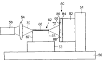
Fig. 1 is the synoptic diagram of above-mentioned conventional optical semiconductor module.Via special use carrier 53 being installed as the luminescence component 62 of laser diode (LD) chip is installed on the module housing 50.Light-receiving module 80 as flat type photodiode (PD) chip is installed on the shell 50 via carrier 51 is installed.Optical fiber 56 and collector lens 54 are fixed on the shell 50 via the fixed cell (not shown).Luminescence component 62 has luminous active coating 66.Light-receiving module 80 has light absorbing zone 84 and optical transport layer 85, and is formed with the impurity diffusion zone 86 as sensitive area in optical transport layer 85.
The forward direction transmission light of launching from the positive side surface 67 of luminescence component 62 70 enters optical fiber 56 by collector lens 54.Simultaneously, launch back emitted light 72, and back emitted light 72 enters the impurity diffusion zone 86 of light-receiving module 80 from back surface 68.Back emitted light 72 is the light that is used to monitor the luminous intensity of forward direction transmission light 70.Therefore, the intensity of back emitted light 72 can be more much lower than the intensity of forward direction transmission light 70.Light-receiving module 80 (LD monitor) is according to the light intensity output electric signal of back emitted light 72.Based on this electric signal, the luminous intensity of control module (not shown) control luminescence component 62.In such a way, the luminous intensity of forward direction transmission light 70 can be maintained constant level.
Japanese kokai publication hei No.5-175614 and 10-321900 disclose optical semiconductor module.In each optical semiconductor module, the installed surface of luminescence component is parallel with the installed surface of light-receiving module, and is reflected from the light of luminescence component emission and then enters light-receiving module.Japanese kokai publication sho No.59-96789 discloses a kind of optical semiconductor module, and wherein, the installed surface of luminescence component is parallel with the installed surface of light-receiving module, and light-receiving module is directly installed on the installed surface, and these are different with conventional structure shown in Figure 1.
Such as the luminescence component of LD from being the surface launching light of side surface with respect to installed surface (will be installed in the face on installation unit etc.).Simultaneously, such as the light-receiving module of PD by being that the face of upper surface receives light with respect to installed surface.Therefore, in conventional structure shown in Figure 1, receive the light of launching from the back surface 68 of luminescence component 62 in the impurity diffusion zone on the upper surface of light-receiving module 80.In order to realize this structure, the installed surface of light-receiving module 80 should be processed to vertical with the installed surface of luminescence component 62.Therefore, as shown in Figure 1, the installation carrier 53 of luminescence component 62 need separate preparation with the installation carrier 51 of light-receiving module 80.As a result, assembling process number, requirement groups number of packages and cost of products increase thus.
In disclosed each structure, luminescence component and light-receiving module can be installed on the same installation carrier in Japanese kokai publication hei No.5-175614 and 10-321900.Yet, need the assembly of preparation reflection from the light of luminescence component emission.As a result, cost of products uprises.According to disclosed technology among the Japanese kokai publication sho No.59-96789, do not need to prepare this assembly, and the increase of cost of products the increase under the situation of conventional structure is so not big as shown in Figure 1.Yet, since the parallel installation of flat type light-receiving module with luminescence component, the luminous sensitivity so luminous sensitivity becomes under the situation that is lower than conventional structure shown in Figure 1.And, because enter by the light absorbing zone outside the sensitive surface, so exist most of incident light can not convert the problem of electric signal to from the additional light of luminescence component.
Summary of the invention
Therefore, an object of the present invention is, a kind of optical semiconductor module and light-receiving module of having eliminated above-mentioned shortcoming is provided.
Purpose more specifically of the present invention is, a kind of optical semiconductor module and light-receiving module that can reduce production costs and can obtain the same high luminous sensitivity of luminous sensitivity with conventional structure is provided.
According to an aspect of the present invention, provide a kind of optical semiconductor module, this optical semiconductor module comprises: luminescence component; Light-receiving module, this light-receiving module thereon the surface and side surface on have sensitive surface, on described sensitive surface, be formed with antireflection film; And installation unit, described luminescence component and described light-receiving module are by on the installation unit as described in being installed in as upper/lower positions relation, promptly, at least be optically coupled in from the light of described luminescence component emission on the described sensitive surface of described side surface of described light-receiving module, wherein, described luminescence component and described light-receiving module are installed on the same plane of described installation unit, and the described upper surface of described light-receiving module is in the horizontal position lower than the upper surface of described luminescence component.Described luminescence component and described light-receiving module can be installed on the same installation unit.Therefore, can reduce process number, requirement groups number of packages and production cost, realize higher luminous sensitivity simultaneously.
According to a further aspect in the invention, a kind of light-receiving module is provided, and this light-receiving module monitoring is from the light of luminescence component emission, and described light-receiving module comprises: sensitive surface, this sensitive surface is formed on the upper surface and side surface of described light-receiving module, and is formed with antireflection film on it.Described luminescence component and described light-receiving module can be installed on the same installation unit.Therefore, can reduce process number and requirement groups number of packages, and can reduce production costs.And, can keep the same high luminous sensitivity of luminous sensitivity with conventional structure.
Description of drawings
Read following detailed description in conjunction with the accompanying drawings, other purpose of the present invention, feature and advantage will become clearer, wherein:
Fig. 1 is the synoptic diagram of conventional optical semiconductor module;
Fig. 2 is the sectional view of light-receiving module;
Fig. 3 is the synoptic diagram according to the optical semiconductor module of first embodiment of the invention;
Fig. 4 is the sectional view according to the light-receiving module of first embodiment;
Fig. 5 A is the sectional view of process that is used to process light-receiving module that illustrates according to first embodiment to 5C;
Fig. 6 A is the sectional view (continuous figure) of process that is used to process light-receiving module that illustrates according to first embodiment to 6C;
Fig. 7 A and 7B are the synoptic diagram according to the optical semiconductor module of second embodiment of the invention;
Fig. 8 is the synoptic diagram according to the optical semiconductor module of third embodiment of the invention;
Fig. 9 is the sectional view according to the light-receiving module of the 3rd embodiment;
Figure 10 is the synoptic diagram according to the optical semiconductor module of four embodiment of the invention;
Figure 11 is the sectional view according to the light-receiving module of the 4th embodiment;
Figure 12 is the sectional view according to the light-receiving module of fifth embodiment of the invention;
Figure 13 is the sectional view according to the light-receiving module of the modification of the 5th embodiment;
Figure 14 is the sectional view according to the light-receiving module of sixth embodiment of the invention;
Figure 15 is the schematic isometric of the light-receiving module of example as a comparison;
Figure 16 is the schematic isometric according to the light-receiving module of seventh embodiment of the invention; And
Figure 17 is the schematic isometric according to the light-receiving module of eighth embodiment of the invention.
Embodiment
In the conventional structure of all structures as shown in Figure 1, light-receiving module 80 generally planar type light-receiving modules.In the flat type light-receiving module, for example, in optical transport layer 85, formed p type impurity diffusion zone 86 by ion implantation technique and diffusion technique.Therefore, easier processing flat type light-receiving module, and this light-receiving module is generally used for optical communication and LD monitoring.Simultaneously, the inventor finds, if with bench-type light-receiving module of the present invention as light-receiving module 80, then can provide have assembling process number still less, the optical semiconductor module of low production cost and excellent luminous sensitivity more.Below, the principle of this light-receiving module is described.
Fig. 2 is the sectional view of bench-type light-receiving module.By n type InGaAs (Gallium indium arsenide) make and have the semiconductor layer 12 of first conductivity type, the light absorbing zone of making by i-InGaAs 14 and the semiconductor layer 16 of making and having second conductivity type (conductivity type relative) with first conductivity type by p type InGaAs, be layered on the semi-insulating substrate 10 of InP (indium phosphide).The outer peripheral portion of layer laminate is removed the same deeply with the semiconductor layer 12 of first conductivity type, to form the platform shape.First electrode of being made by AuGe (gold-germanium alloy) 22 is connected to the semiconductor layer 12 of first conductivity type.Second electrode of being made by AuZn (golden kirsite) 24 is connected to the semiconductor layer 16 of second conductivity type.The diaphragm of being made by SiN (silicon nitride) 17 is formed on sensitive area 21 outsides on the upper surface 34, to contact with for example side surface 32.The antireflection film of being made by SiN 18 is formed on sensitive area 21 and the diaphragm 17.First electrode 22 and second electrode 24 are via be connected to the pad of being made by Au 28 (not shown interconnection portion and the pad that is connected to second electrode 24) by the interconnection portion 26 that Ti (titanium)/Pt (platinum)/Au (gold) makes.The metal film of being made by Ti/Pt/Au 30 was formed under substrate 10 following.
Bench-type light-receiving module shown in Figure 2 is applied to voltage between the semiconductor layer 16 of the semiconductor layer 12 of first conductivity type and second conductivity type.The light that is incident on the sensitive area 21 is absorbed by light absorbing zone 14, and electric current flows between the semiconductor layer 16 of the semiconductor layer 12 of first conductivity type and second conductivity type.This electric current is output as electric signal.
In this bench-type light-receiving module, the semiconductor layer 12 of first conductivity type and the semiconductor layer 16 of second conductivity type also are present in upper surface and the below that light absorbing zone 14 is arranged in the part of side surface 32 neighborhoods, as shown in Figure 2.Utilize this structure, can convert the light that is incident on the light absorbing zone 14 by side surface 32 to electric signal.Under the situation of flat type light-receiving module, as shown in Figure 1, the impurity diffusion zone 86 that is equal to the semiconductor layer 16 of second conductivity type exists only on the part of luminescent layer 85.Utilize this structure, even light enters light-receiving module by side surface, the major part that is incident in the light on the light absorbing zone 14 by this side surface because not being stored in light absorbing zone 84, impurity diffusion zone 86 is not arranged on the part of neighborhood of this side surface, so can not be converted into electric signal.
In this bench-type light-receiving module, need to reduce dark current, make and can in being subjected to optical module, use this light-receiving module.Therefore, on the side surface 32 of platform portion, formed the diaphragm 17 (passivating film) that is used to reduce leakage current.Utilize this structure, sensitive area 21 is formed on the upper surface 34 of platform portion, even and light-receiving module and LD chip be installed in the same plane, can not obtain to be used to monitor the abundant luminous sensitivity of LD.Because the above-mentioned fact, so do not use the bench-type light-receiving module usually as the LD monitor.In order to address this is that, the inventor has developed light-receiving module of the present invention based on following discovery.Under with the situation of light-receiving module, and be unlike in and equally wish to reduce dark current under the situation that light-receiving module is used to receive as the optical monitoring device.Therefore, do not adopt diaphragm 17, and antireflection film 18 can be finished the light-receiving module as monitoring assembly separately.
Principle of the present invention is, can be received the light-receiving module reception of the light on the side surface that is incident on platform portion from the light of the side surface emission of luminescence component.Utilize this structure, the installed surface of luminescence component and the installed surface of light-receiving module can be set parallel to each other.Therefore, process number and requirement groups number of packages are lacked than under the regular situation, and can reduce production costs, keep sufficient luminous sensitivity simultaneously.Below, embodiments of the present invention are described.
[first embodiment]
Fig. 3 is the synoptic diagram according to the optical semiconductor module of first embodiment of the invention.Luminescence component 62 for example is Fabry-Perot LD or distributed Feedback LD.Light-receiving module 60 is following bench-type light-receiving modules that will describe in detail, and has the platform portion that is formed on the substrate 10.Different with structure shown in Figure 1, this optical semiconductor module has luminescence component 62 and the light-receiving module 60 that is installed on the installation carrier 52.The side surface 32 of light-receiving module 60 receives back to light from back surface 68 emissions of luminescence component 62.Therefore identical in the others of this structure and the structure shown in Figure 1, omitted the explanation to them here.
Fig. 4 is the sectional view of the light-receiving module 60 that adopts in first embodiment.Different with light-receiving module shown in Figure 2, light-receiving module 60 does not have diaphragm, but has the side surface 32 that is formed directly into platform portion 20 and the antireflection film 18 on the upper surface 34.Therefore identical in the others of this structure and the structure shown in Figure 2, omitted the explanation to them here.
Fig. 5 A is the sectional view that the process that is used to process light-receiving module 60 is shown to 6C.Shown in Fig. 5 A, by on InP substrate 10, the grow semiconductor layer 16 of semiconductor layer 12, light absorbing zone 14 and second conductivity type of first conductivity type of MOCVD (Organometallic Chemistry vapor deposition method).Shown in Fig. 5 B, on the predetermined portions of the semiconductor layer 12 of semiconductor layer 16, light absorbing zone 14 and first conductivity type of second conductivity type, carry out etching, to form platform portion 20.Shown in Fig. 5 C, has 100nm to the film thickness of 300nm and the antireflection film of making by SiN 18 by CVD formation.
As shown in Figure 6A, form first electrode 22 and second electrode 24 that will be connected to the semiconductor layer 16 of second conductivity type of the semiconductor layer 12 that will be connected to first conductivity type by vapor deposition techniques.Shown in Fig. 6 B, form the interconnection portion 26 that will be connected to first electrode 22 and second electrode 24 by vapor deposition techniques.Also form the pad 28 that will be connected to interconnection portion 26 by the plating technology.Shown in Fig. 6 C, from following polishing substrate 10, thereby with substrate 10 attenuates.Then, below the bottom surface, form metal film 30 by vapor deposition techniques.In such a way, finish light-receiving module 60.
Here, the difference between light-receiving module shown in Figure 2 and the light-receiving module shown in Figure 4 is described.In light-receiving module shown in Figure 2, diaphragm 17 is not present on the semiconductor layer 16 of second conductivity type that forms upper surface 34, but antireflection film 18 is formed on the semiconductor layer 16 of second conductivity type that forms upper surface 34.This antireflection film 18 prevents to reflect the light of predetermined wavelength.Yet diaphragm 17 and antireflection film 18 all are present on the side surface 32.As a result, reflected the light that is incident on the predetermined wavelength on the side surface 32.On the other hand, in light-receiving module shown in Figure 4 60, do not form diaphragm 17 (passivating film), thus, can prevent to be incident on the reflection of light of the predetermined wavelength on the side surface 32.In Fig. 2, diaphragm 17 is set, to reduce the dark current that will generate because of the leakage current in the neighborhood of side surface 32.The light-receiving module 60 that is used to monitor LD is not strict for dark current.Therefore, the light-receiving module that does not have diaphragm 17 60 usefulness as shown in Figure 4 can be acted on the light-receiving module of monitoring LD.
In the first embodiment, optical semiconductor module has via installing that carrier 52 (installation unit) is installed on the shell 50 and being installed on the shell 50 and by side surface 32 and receiving from the light-receiving module 60 of the light of luminescence component 62 emissions from side surface 68 radiative luminescence components 62 with via carrier 52 is installed.More particularly, light-receiving module 60 has the antireflection film 18 that is formed on upper surface 34 and the side surface 32.Therefore, light-receiving module 60 has the sensitive surface that is formed with antireflection film 18 on upper surface 34 and side surface 32.On as the installation carrier 52 of installation unit, luminescence component 62 and light-receiving module 60 are installed by concerning as upper/lower positions, that is, this position relation be retained as from the light of luminescence component 62 emissions at least optics be connected on the sensitive surface on the side surface 32 of light-receiving module 60.Utilize this structure, luminescence component 62 and light-receiving module 60 can be installed on the same installation carrier 52.Therefore, luminescence component 62 and light-receiving module 60 can be installed on the same plane that carrier 52 is installed.Thus, can reduce process number and requirement groups number of packages, can reduce production costs, and can obtain higher luminous sensitivity.
And, as shown in Figure 4, preferably, the semiconductor layer 12 of first conductivity type of light-receiving module 60 and the semiconductor layer of second conductivity type 16 contact side surfaces 32.In other words, preferably, the semiconductor layer 16 of at least the second conductivity type extends on the side surface 32.Utilize this structure, can convert the light that is incident on the light absorbing zone 14 by side surface 32 to electric signal.Therefore, the bench-type light-receiving module is preferred.
[second embodiment]
Fig. 7 A is the synoptic diagram according to the optical semiconductor module of second embodiment of the invention.Different with the optical semiconductor module of first embodiment shown in Figure 3, for example, this optical semiconductor module has the upper surface 34 of the light-receiving module 60 that is in the horizontal position lower than the active coating 66 of luminescence component 62.Therefore identical in the others of this structure and the structure shown in Figure 3, omitted the explanation to them here.
Because the upper surface 34 of light-receiving module 60 is positioned at the horizontal position lower than the active coating 66 of luminescence component 62, so the side surface 32 of light-receiving module 60 can receive back to light 72a from back surface 68 emission of luminescence component 62, and the upper surface 34 of light-receiving module 60 can receive the back to emission light 72b, shown in Fig. 7 B.Utilize this structure, can increase light-receiving module 60 at the luminous sensitivity of back to emission light 72.
With the same in second embodiment, preferably, the upper surface 34 of light-receiving module 60 is positioned at the horizontal position lower than the active coating 66 of luminescence component 62.Yet active coating 66 is only hanged down about 1 μ m than the upper surface 69 of luminescence component 62.On the other hand, the thickness of each in luminescence component 62 and the light-receiving module 60 all is approximately 100 μ m.Therefore, the difference in height h1 between the upper surface 34 of the active coating 66 of luminescence component 62 and light-receiving module 60 is substantially equal to the difference in height h2 between the upper surface 34 of the upper surface 69 of luminescence component 62 and light-receiving module 60.Therefore, in the practice, the upper surface 34 of light-receiving module 60 is lower than the upper surface 69 of luminescence component 62 at least.
The thickness of luminescence component 62 is generally 100 μ m to 150 μ m.Therefore, the thickness of light-receiving module 60 should be preferably 100 μ m or following.
[the 3rd embodiment]
Fig. 8 is the synoptic diagram according to the optical semiconductor module of third embodiment of the invention.Different with the optical semiconductor module of first embodiment shown in Figure 3, for example, this optical semiconductor module has the highly reflecting films 36 (HR) on the side surface 33 that is formed on a side relative with side surface 32, enters light-receiving module 60 from the light 72 in the face of luminescence component 62 emissions of light-receiving module 60 by side surface 32.Fig. 9 is the sectional view of light-receiving module 60 shown in Figure 8.Different with light-receiving module shown in Figure 4, this light-receiving module 60 has the highly reflecting films 36 on the side surface 33 on the side relative with side surface 32 that is formed on light-receiving module 60.Highly reflecting films 36 can be in order with having the SiO of 200nm to the film thickness of 300nm from side surface
2(silicon dioxide) film/the have TiO of 100nm to the film thickness of 200nm
2(titanium dioxide) film formed film, perhaps with have 50nm to the TiON (titanium-nitrogen-oxygen thing) of the film thickness of 200nm, have 50nm to the Si film of the film thickness of 200nm, have 100nm to the Au film of the film thickness of 200nm, have 100nm to the Ag film of the film thickness of 200nm, have the film of 100nm to the formation such as AuGe film of the film thickness of 200nm.This highly reflecting films 36 can for example form by sputtering technology or vacuum vapor deposition technology.Therefore identical in the structure of the others of this structure and Fig. 3 and first embodiment shown in 4, omitted the explanation to them here.
According to the 3rd embodiment, as shown in Figure 8, the light 72c that advances by platform portion 20 is reflected by highly reflecting films 36.Light 72c is a part that is incident on the light in the platform portion 20 of light-receiving module 60.When advancing by light absorbing zone 14 once more, reflected light 72d is absorbed by light absorbing zone 14.Thus, can increase the luminous sensitivity of light-receiving module 60 at emission light 72.
[the 4th embodiment]
Figure 10 is the synoptic diagram according to the optical semiconductor module of four embodiment of the invention.Figure 11 is the sectional view according to the light-receiving module of the 4th embodiment.Different with the structure of the second and the 3rd embodiment shown in Fig. 7 A and Fig. 8 difference, this optical semiconductor module has the side surface 32a of the light-receiving module 60 that forms with the shape of falling from power.Therefore identical in the others of this structure and Fig. 7 A and the structure shown in 8, omitted the explanation to them here.This portion of falling from power can form by wet etching in conjunction with the advantage of high preferred orientation.
According to the 4th embodiment, the upper surface 34 of light-receiving module 60 is positioned at the horizontal position lower than the upper surface 69 of luminescence component 62.Therefore, the light 72a that advances along oblique direction down enters light-receiving module 60 by side surface 32a.Because side surface 32a is the shape of falling from power, thus be incident on the light absorbing zone 14 refract light 72e roughly along continuous straight runs advance.Therefore, light 72e takes a long time through light absorbing zone 14, and light absorbing zone 14 easy absorbing light 72e.Thus, can further increase the luminous sensitivity of light-receiving module 60 at emission light 72a.Here, preferably, wait the angle of determining the portion of falling from power based on the refractive index of the distance between light-receiving module 60 and the luminescence component 62, height h1, light absorbing zone 14.
[the 5th embodiment]
Figure 12 is the sectional view according to the light-receiving module 60 of the optical semiconductor module of fifth embodiment of the invention.Different with the antireflection film of first embodiment shown in Figure 4, antireflection film 18 is formed with two-layer: diaphragm 18a, it is to have the SiO of 50nm to the film thickness of 200nm
2Film; With adjusting film 18b, it is to have the SiN film of 50nm to the film thickness of 200nm.Diaphragm 18a is protection side surface 32 and 33 and prevent the film of the leakage current between the semiconductor layer 16 of the semiconductor layer 12 of first conductivity type and second conductivity type.Regulating film 18b is to regulate the incident light wavelength so that antireflection film 18 has the film of the function of reflecting of preventing.Utilize this structure, diaphragm 18a can prevent above-mentioned leakage current, as the diaphragm 17 of light-receiving module shown in Figure 2.And diaphragm 18a and adjusting film 18b cooperate each other, to prevent the reflection of light of predetermined wavelength.Figure 13 illustration the modification of the 5th embodiment.Different with the diaphragm 18a of the 5th embodiment shown in Figure 12, diaphragm 18c is made by i-InP.As mentioned above, antireflection film 18 should be preferably contacts with part on 33 with the side surface 32 that is positioned at of light absorbing zone 14.Antireflection film 18 can be a monofilm as in first embodiment, also can be the multilayer film with two-layer or more multi-layered formation as in the 5th embodiment.And the diaphragm 18a (18c) in the antireflection film 18 can be a dielectric film as in the 5th embodiment, can be semiconductor film as in the modification of the 5th embodiment also.
[the 6th embodiment]
Figure 14 is the sectional view according to the light-receiving module 60 of the optical semiconductor module of sixth embodiment of the invention.The difference of this embodiment and first embodiment shown in Figure 4 is that the semiconductor layer 12a of first conductivity type is made by n type InP, and the semiconductor layer 16a of second conductivity type is made by p type InP.With the same in the 6th embodiment, can select the material of light-receiving module 60 and luminescence component 62 arbitrarily.
[the 7th embodiment]
Figure 15 is the schematic isometric of the light-receiving module of example as a comparison.Substrate 10 is provided with platform portion 20.The upper surface 34 of platform portion 20 is provided with second electrode 24.Semiconductor layer (not shown) around platform portion 20 first conductivity types is provided with first electrode 22.First pad 28 and second pad 29 are arranged on the substrate 10, and are connected to first electrode 22 and second electrode 24 via interconnection portion 26 and 27 respectively.Other interconnection portion (not shown) is connected to first pad 28 and second pad 29, and for example electric signal can be read the control module (not shown) by interconnection portion from light-receiving module.In this comparative example, advance along the direction of first pad 28 from the light 72 of luminescence component 62 emissions.As a result, the part of the emission light 72 interconnection portion that is connected to first pad 28 disperses.
Figure 16 is the schematic isometric according to the light-receiving module of seventh embodiment of the invention.The upper surface of the platform portion 20 of light-receiving module is provided with second electrode 24.Be provided with first electrode 22 around platform portion 20. Interconnection portion 26 and 27 is connected to first electrode 22 and second electrode 24, and extends to the outside of sensitive surface.First pad 28 and second pad 29 (electrode pad) are connected to interconnection portion 26 and 27.The difference of this embodiment and comparative example shown in Figure 15 is, first pad 28 and second pad 29 are arranged on the side relative with luminescence component 62 of platform portion 20 of light-receiving module.Different with comparative example, this embodiment does not make emission light 72 be disperseed by interconnection portion, thereby can further increase the luminous sensitivity of light-receiving module 60 at emission light 72.
And first pad 28 is arranged on the both sides of second pad 29.Because interconnection portion 26 should be connected in first pad 28 any, so intersect with the interconnection portion that is connected to second pad 29 no matter the position of the pad of the shell side of optical semiconductor module how, can prevent each the interconnection portion that is connected to each other to first pad 28.
[the 8th embodiment]
Figure 17 is the schematic isometric according to the light-receiving module of eighth embodiment of the invention.The difference of this light-receiving module shown in Figure 17 and light-receiving module shown in Figure 16 is that the 20b of platform portion has the quadrangular shape.Therefore, side surface 32b is a flat surfaces.Utilize this structure, emission light 72 enters by side surface 32b.Thus, can make light-receiving module 60 higher at the luminous sensitivity of emission light 72.In a plurality of side surfaces of the 20b of platform portion, make the side surface that enters of emission light 72 should be flat surfaces, and in other side surface each can have curved surface.
In first to the 8th embodiment, luminescence component 62 and light-receiving module 60 can be directly installed on the shell 50.In other words, shell 50 can also be as the installation unit that luminescence component 62 and light-receiving module 60 will directly be installed.And in the above-described embodiment, the semiconductor layer 12 of first conductivity type is the n type, and the semiconductor layer 16 of second conductivity type is the p type.Yet the semiconductor layer 12 of first conductivity type and the semiconductor layer 16 of second conductivity type should only be opposite conductivity type.Therefore, the semiconductor layer 12 of first conductivity type can be the p type, and the semiconductor layer 16 of second conductivity type can be the n type.
In first to the 8th embodiment, the bench-type photodiode has been described as light-receiving module.Yet the present invention can also be applied to the light-receiving module of other type, as p-i-n photodiode and avalanche-type photodiode (APD).
Although illustrated and described several preferred implementation of the present invention, but it should be apparent to those skilled in the art that, without departing from the principles and spirit of the present invention, can change these embodiments, scope of the present invention limits in claim and equivalent thereof.
The Japanese patent application No.2007-086131 that the application submitted to based on March 29th, 2007, its whole disclosures are incorporated into this.
Claims (14)
1. optical semiconductor module, this optical semiconductor module comprises:
Luminescence component;
Light-receiving module, this light-receiving module are the bench-type photodiodes, and have sensitive surface on the upper surface of the platform portion of described light-receiving module and side surface, directly are formed with antireflection film on described upper surface and side surface; And
Installation unit, on this installation unit by luminescence component as described in installing as upper/lower positions relation and as described in light-receiving module, that is, make from the light of described luminescence component emission to be optically coupled at least on the described sensitive surface of described side surface of described light-receiving module,
Wherein, described luminescence component and described light-receiving module are installed on the same plane of described installation unit, and the described upper surface of described light-receiving module is in the horizontal position lower than the upper surface of described luminescence component.
2. optical semiconductor module according to claim 1, this optical semiconductor module also comprises:
Reflectance coating, this reflectance coating be set at described light-receiving module with in the face of on the opposite side surface on the relative side of the side surface of described luminescence component.
3. optical semiconductor module according to claim 1, wherein, described light-receiving module has the side surface of the shape of falling from power.
4. optical semiconductor module according to claim 1, wherein, the described side surface of described light-receiving module has flat surfaces.
5. optical semiconductor module according to claim 1, wherein:
Described light-receiving module has the semiconductor layer of light absorbing zone, first conductivity type, and the semiconductor layer of second conductivity type, and described light absorbing zone is inserted between the described semiconductor layer of the described semiconductor layer of described first conductivity type and described second conductivity type; And
Described optical semiconductor module also comprises first pad and second pad, described first pad and described second pad are arranged on the side relative with described luminescence component of platform portion of described light-receiving module, and are connected to the described semiconductor layer of described first conductivity type and the described semiconductor layer of described second conductivity type respectively.
6. optical semiconductor module according to claim 5 wherein, described first pad is arranged on the both sides of described second pad.
7. optical semiconductor module according to claim 1, wherein, described antireflection film is a multilayer film.
8. optical semiconductor module according to claim 1, wherein:
Described light-receiving module has the semiconductor layer of light absorbing zone, first conductivity type, and the semiconductor layer of second conductivity type, and described light absorbing zone is inserted between the described semiconductor layer of the described semiconductor layer of described first conductivity type and described second conductivity type; And
The semiconductor layer of the semiconductor layer of described first conductivity type and described second conductivity type contacts described side surface.
9. optical semiconductor module according to claim 2, wherein, described reflectance coating is by SiO
2/ TiO
2, a kind of the making among TiON, Si, Au, Ag and the AuGe.
10. light-receiving module, this light-receiving module monitoring be from the light of luminescence component emission,
Described light-receiving module is the bench-type photodiode, and described light-receiving module comprises:
Sensitive surface, this sensitive surface are formed on the upper surface and side surface of platform portion of described light-receiving module, and directly are formed with antireflection film on described upper surface and side surface.
11. light-receiving module according to claim 10, wherein, the side surface of described light-receiving module forms the shape of falling from power.
12. light-receiving module according to claim 10, this light-receiving module also comprises:
Reflectance coating, this reflectance coating are formed on other side surface the described side surface in being arranged on described sensitive surface of described light-receiving module.
13. light-receiving module according to claim 12, wherein, described reflectance coating is by SiO
2/ TiO
2, a kind of the making among TiON, Si, Au, Ag and the AuGe.
14. light-receiving module according to claim 10, this light-receiving module also comprises:
Electrode, this electrode are formed on the described upper surface of described light-receiving module;
Interconnection portion, this interconnection portion is connected to described electrode, and extends to the outside of described sensitive surface; And
Electrode pad, this electrode pad are connected to described interconnection portion.
Applications Claiming Priority (2)
| Application Number | Priority Date | Filing Date | Title |
|---|---|---|---|
| JP2007086131A JP5197978B2 (en) | 2007-03-29 | 2007-03-29 | Optical semiconductor module |
| JP2007-086131 | 2007-03-29 |
Publications (2)
| Publication Number | Publication Date |
|---|---|
| CN101276028A CN101276028A (en) | 2008-10-01 |
| CN101276028B true CN101276028B (en) | 2011-05-04 |
Family
ID=39650540
Family Applications (1)
| Application Number | Title | Priority Date | Filing Date |
|---|---|---|---|
| CN2008100883644A Active CN101276028B (en) | 2007-03-29 | 2008-03-28 | Optical semiconductor module and light receiving element |
Country Status (5)
| Country | Link |
|---|---|
| US (1) | US7807954B2 (en) |
| EP (1) | EP1976023A3 (en) |
| JP (1) | JP5197978B2 (en) |
| CN (1) | CN101276028B (en) |
| TW (1) | TWI378662B (en) |
Families Citing this family (6)
| Publication number | Priority date | Publication date | Assignee | Title |
|---|---|---|---|---|
| TWI490576B (en) * | 2010-11-29 | 2015-07-01 | Hon Hai Prec Ind Co Ltd | Optical transmission system |
| US9318639B2 (en) * | 2013-09-17 | 2016-04-19 | Finisar Corporation | Gallium arsenide avalanche photodiode |
| JP2015162576A (en) * | 2014-02-27 | 2015-09-07 | 住友電気工業株式会社 | Semiconductor optical integrated element and semiconductor optical integrated element manufacturing method |
| JP2017163023A (en) * | 2016-03-10 | 2017-09-14 | 株式会社東芝 | Photodetector and subject detection system using the same |
| US10937919B2 (en) | 2016-05-16 | 2021-03-02 | Sony Corporation | Light receiving element, optical communication device, and method for manufacturing a light receiving element |
| US11909172B2 (en) * | 2020-01-08 | 2024-02-20 | Asahi Kasei Kabushiki Kaisha | Method for manufacturing optical device and optical device |
Family Cites Families (23)
| Publication number | Priority date | Publication date | Assignee | Title |
|---|---|---|---|---|
| JPS57160189A (en) | 1981-03-30 | 1982-10-02 | Hitachi Ltd | Semiconductor luminous device incorporated with photodetector |
| JPS5947778A (en) * | 1982-09-10 | 1984-03-17 | Hitachi Ltd | Semiconductor photo receiving element and laser oscillation device using it |
| JPS5996789A (en) | 1982-11-25 | 1984-06-04 | Nec Corp | Photosemiconductor device |
| JPH07123170B2 (en) * | 1990-08-07 | 1995-12-25 | 光計測技術開発株式会社 | Light receiving element |
| US5093576A (en) * | 1991-03-15 | 1992-03-03 | Cree Research | High sensitivity ultraviolet radiation detector |
| JPH0582827A (en) * | 1991-09-19 | 1993-04-02 | Nec Corp | Semiconductor light receiving element |
| JPH05175614A (en) | 1991-12-26 | 1993-07-13 | Canon Inc | Optical semiconductor device |
| JP2748917B2 (en) * | 1996-03-22 | 1998-05-13 | 日本電気株式会社 | Semiconductor device |
| KR100688240B1 (en) * | 1997-01-09 | 2007-03-02 | 니치아 카가쿠 고교 가부시키가이샤 | Nitride Semiconductor Device |
| JPH10321900A (en) | 1997-05-14 | 1998-12-04 | Sumitomo Electric Ind Ltd | Optical module |
| US6353250B1 (en) * | 1997-11-07 | 2002-03-05 | Nippon Telegraph And Telephone Corporation | Semiconductor photo-detector, semiconductor photo-detection device, and production methods thereof |
| JP2000151013A (en) | 1998-11-13 | 2000-05-30 | Furukawa Electric Co Ltd:The | Optical transmission/reception integrated element |
| US6331379B1 (en) * | 1999-09-01 | 2001-12-18 | Micron Technology, Inc. | Photo-lithography process using multiple anti-reflective coatings |
| US6525347B2 (en) * | 2001-03-12 | 2003-02-25 | Matsushita Electric Industrial Co., Ltd. | Photodetector and unit mounted with photodetector |
| JP2003198032A (en) * | 2001-12-27 | 2003-07-11 | Mitsubishi Electric Corp | Optical element, optical element module, and carrier for the optical element |
| JP2003209268A (en) * | 2002-01-11 | 2003-07-25 | Mitsubishi Electric Corp | Optical module |
| JP2003303975A (en) * | 2002-04-08 | 2003-10-24 | Opnext Japan Inc | Optical module with photodiode for monitoring |
| JP2004047831A (en) * | 2002-07-12 | 2004-02-12 | Mitsubishi Electric Corp | Light receiving element module |
| JP2006032567A (en) * | 2004-07-14 | 2006-02-02 | Sanyo Electric Co Ltd | Photo detector and its manufacturing method |
| JP4755854B2 (en) * | 2005-06-02 | 2011-08-24 | 富士通株式会社 | Semiconductor light receiving device and manufacturing method thereof |
| DE102005025782B4 (en) * | 2005-06-04 | 2007-02-22 | Diehl Ako Stiftung & Co. Kg | Touch-sensitive pushbutton |
| JP2007086131A (en) | 2005-09-20 | 2007-04-05 | Konica Minolta Business Technologies Inc | Electrophotographic photoreceptor and image forming apparatus |
| JP2008010710A (en) * | 2006-06-30 | 2008-01-17 | Oki Electric Ind Co Ltd | Semiconductor laser device |
-
2007
- 2007-03-29 JP JP2007086131A patent/JP5197978B2/en active Active
-
2008
- 2008-03-26 TW TW097110754A patent/TWI378662B/en not_active IP Right Cessation
- 2008-03-27 EP EP08153472.9A patent/EP1976023A3/en not_active Withdrawn
- 2008-03-28 CN CN2008100883644A patent/CN101276028B/en active Active
- 2008-03-31 US US12/059,232 patent/US7807954B2/en active Active
Non-Patent Citations (2)
| Title |
|---|
| JP昭57-160189A 1982.10.02 |
| JP特开2000-151013A 2000.05.30 |
Also Published As
| Publication number | Publication date |
|---|---|
| US7807954B2 (en) | 2010-10-05 |
| TW200845615A (en) | 2008-11-16 |
| JP5197978B2 (en) | 2013-05-15 |
| EP1976023A3 (en) | 2014-03-26 |
| US20080237452A1 (en) | 2008-10-02 |
| JP2008244368A (en) | 2008-10-09 |
| TWI378662B (en) | 2012-12-01 |
| CN101276028A (en) | 2008-10-01 |
| EP1976023A2 (en) | 2008-10-01 |
Similar Documents
| Publication | Publication Date | Title |
|---|---|---|
| US5787215A (en) | Linear PD/LD module, linear PD/LED module, linear LD/PD module, linear LED/PD module and linear PD module | |
| CN101276028B (en) | Optical semiconductor module and light receiving element | |
| US5218223A (en) | Opto-electronic semiconductor component | |
| JP2002289904A (en) | Semiconductor light-receiving element and its manufacturing method | |
| JP3734939B2 (en) | Light receiving element and light receiving element module | |
| US6909083B2 (en) | Photodetector and unit mounted with photodetector | |
| US8330243B2 (en) | Semiconductor light-receiving element and optical module | |
| KR100464333B1 (en) | Photo detector and method for fabricating thereof | |
| JPH0677518A (en) | Semiconductor photodetector | |
| KR102093168B1 (en) | Photodetector having double light path | |
| EP3792983B1 (en) | Light-receiving element unit | |
| US20030122061A1 (en) | Optical device, optical device module and carrier for optical device | |
| US20220173259A1 (en) | Photoreceiver and Optical Receiver | |
| US6989554B2 (en) | Carrier plate for opto-electronic elements having a photodiode with a thickness that absorbs a portion of incident light | |
| JP6660282B2 (en) | Light receiving element | |
| JP3427125B2 (en) | Semiconductor device with optical lens function | |
| JP3538731B2 (en) | Submount for receiving photodiode | |
| KR20180111200A (en) | Semiconductor device package and optical assembly | |
| JP2004241681A (en) | Semiconductor light receiver and method of manufacturing the same | |
| JP2008010710A (en) | Semiconductor laser device | |
| JPH1117211A (en) | Semiconductor planar photodiode and device therewith | |
| JPH05136446A (en) | Semiconductor photodetector | |
| JP2001308366A (en) | Photodiode | |
| JP2001308369A (en) | Photodiode | |
| JP2003282931A (en) | Photo diode and optical communication module |
Legal Events
| Date | Code | Title | Description |
|---|---|---|---|
| C06 | Publication | ||
| PB01 | Publication | ||
| C10 | Entry into substantive examination | ||
| SE01 | Entry into force of request for substantive examination | ||
| C14 | Grant of patent or utility model | ||
| GR01 | Patent grant |