CN101246887B - Sensing FET integrated with a high-voltage vertical transistor - Google Patents
Sensing FET integrated with a high-voltage vertical transistor Download PDFInfo
- Publication number
- CN101246887B CN101246887B CN2008100807528A CN200810080752A CN101246887B CN 101246887 B CN101246887 B CN 101246887B CN 2008100807528 A CN2008100807528 A CN 2008100807528A CN 200810080752 A CN200810080752 A CN 200810080752A CN 101246887 B CN101246887 B CN 101246887B
- Authority
- CN
- China
- Prior art keywords
- post
- transistor
- semiconductor device
- source area
- tagma
- Prior art date
- Legal status (The legal status is an assumption and is not a legal conclusion. Google has not performed a legal analysis and makes no representation as to the accuracy of the status listed.)
- Active
Links
- 239000004065 semiconductor Substances 0.000 claims abstract description 51
- 239000000758 substrate Substances 0.000 claims abstract description 28
- 230000005669 field effect Effects 0.000 claims abstract description 23
- 239000000463 material Substances 0.000 claims abstract description 13
- 238000005070 sampling Methods 0.000 claims description 6
- 238000002955 isolation Methods 0.000 claims description 2
- 238000009413 insulation Methods 0.000 claims 2
- 229910052710 silicon Inorganic materials 0.000 description 24
- 239000010703 silicon Substances 0.000 description 24
- XUIMIQQOPSSXEZ-UHFFFAOYSA-N Silicon Chemical compound [Si] XUIMIQQOPSSXEZ-UHFFFAOYSA-N 0.000 description 12
- 238000010586 diagram Methods 0.000 description 8
- 230000011218 segmentation Effects 0.000 description 6
- 238000000034 method Methods 0.000 description 4
- 210000001331 nose Anatomy 0.000 description 4
- 239000013078 crystal Substances 0.000 description 3
- 239000003989 dielectric material Substances 0.000 description 3
- 238000005516 engineering process Methods 0.000 description 3
- VYPSYNLAJGMNEJ-UHFFFAOYSA-N Silicium dioxide Chemical compound O=[Si]=O VYPSYNLAJGMNEJ-UHFFFAOYSA-N 0.000 description 2
- 230000008878 coupling Effects 0.000 description 2
- 238000010168 coupling process Methods 0.000 description 2
- 238000005859 coupling reaction Methods 0.000 description 2
- 239000002184 metal Substances 0.000 description 2
- 229910021420 polycrystalline silicon Inorganic materials 0.000 description 2
- 229920005591 polysilicon Polymers 0.000 description 2
- 238000000926 separation method Methods 0.000 description 2
- 229910052581 Si3N4 Inorganic materials 0.000 description 1
- 230000015572 biosynthetic process Effects 0.000 description 1
- 239000003990 capacitor Substances 0.000 description 1
- 238000005229 chemical vapour deposition Methods 0.000 description 1
- 239000012141 concentrate Substances 0.000 description 1
- 239000004020 conductor Substances 0.000 description 1
- 238000009792 diffusion process Methods 0.000 description 1
- 238000009826 distribution Methods 0.000 description 1
- 230000005684 electric field Effects 0.000 description 1
- 230000005611 electricity Effects 0.000 description 1
- 230000008030 elimination Effects 0.000 description 1
- 238000003379 elimination reaction Methods 0.000 description 1
- 230000014509 gene expression Effects 0.000 description 1
- 238000004519 manufacturing process Methods 0.000 description 1
- 229910001092 metal group alloy Inorganic materials 0.000 description 1
- 238000001465 metallisation Methods 0.000 description 1
- 230000004048 modification Effects 0.000 description 1
- 238000012986 modification Methods 0.000 description 1
- 229910021332 silicide Inorganic materials 0.000 description 1
- FVBUAEGBCNSCDD-UHFFFAOYSA-N silicide(4-) Chemical compound [Si-4] FVBUAEGBCNSCDD-UHFFFAOYSA-N 0.000 description 1
- 239000000377 silicon dioxide Substances 0.000 description 1
- 235000012239 silicon dioxide Nutrition 0.000 description 1
- HQVNEWCFYHHQES-UHFFFAOYSA-N silicon nitride Chemical compound N12[Si]34N5[Si]62N3[Si]51N64 HQVNEWCFYHHQES-UHFFFAOYSA-N 0.000 description 1
- 239000002210 silicon-based material Substances 0.000 description 1
Images


Classifications
-
- H—ELECTRICITY
- H01—ELECTRIC ELEMENTS
- H01L—SEMICONDUCTOR DEVICES NOT COVERED BY CLASS H10
- H01L29/00—Semiconductor devices adapted for rectifying, amplifying, oscillating or switching, or capacitors or resistors with at least one potential-jump barrier or surface barrier, e.g. PN junction depletion layer or carrier concentration layer; Details of semiconductor bodies or of electrodes thereof ; Multistep manufacturing processes therefor
- H01L29/66—Types of semiconductor device ; Multistep manufacturing processes therefor
- H01L29/68—Types of semiconductor device ; Multistep manufacturing processes therefor controllable by only the electric current supplied, or only the electric potential applied, to an electrode which does not carry the current to be rectified, amplified or switched
- H01L29/76—Unipolar devices, e.g. field effect transistors
- H01L29/772—Field effect transistors
- H01L29/78—Field effect transistors with field effect produced by an insulated gate
- H01L29/7801—DMOS transistors, i.e. MISFETs with a channel accommodating body or base region adjoining a drain drift region
- H01L29/7802—Vertical DMOS transistors, i.e. VDMOS transistors
- H01L29/7815—Vertical DMOS transistors, i.e. VDMOS transistors with voltage or current sensing structure, e.g. emulator section, overcurrent sensing cell
-
- H—ELECTRICITY
- H01—ELECTRIC ELEMENTS
- H01L—SEMICONDUCTOR DEVICES NOT COVERED BY CLASS H10
- H01L29/00—Semiconductor devices adapted for rectifying, amplifying, oscillating or switching, or capacitors or resistors with at least one potential-jump barrier or surface barrier, e.g. PN junction depletion layer or carrier concentration layer; Details of semiconductor bodies or of electrodes thereof ; Multistep manufacturing processes therefor
- H01L29/66—Types of semiconductor device ; Multistep manufacturing processes therefor
- H01L29/68—Types of semiconductor device ; Multistep manufacturing processes therefor controllable by only the electric current supplied, or only the electric potential applied, to an electrode which does not carry the current to be rectified, amplified or switched
- H01L29/76—Unipolar devices, e.g. field effect transistors
- H01L29/772—Field effect transistors
- H01L29/78—Field effect transistors with field effect produced by an insulated gate
- H01L29/7801—DMOS transistors, i.e. MISFETs with a channel accommodating body or base region adjoining a drain drift region
- H01L29/7802—Vertical DMOS transistors, i.e. VDMOS transistors
- H01L29/7813—Vertical DMOS transistors, i.e. VDMOS transistors with trench gate electrode, e.g. UMOS transistors
-
- H—ELECTRICITY
- H01—ELECTRIC ELEMENTS
- H01L—SEMICONDUCTOR DEVICES NOT COVERED BY CLASS H10
- H01L29/00—Semiconductor devices adapted for rectifying, amplifying, oscillating or switching, or capacitors or resistors with at least one potential-jump barrier or surface barrier, e.g. PN junction depletion layer or carrier concentration layer; Details of semiconductor bodies or of electrodes thereof ; Multistep manufacturing processes therefor
- H01L29/02—Semiconductor bodies ; Multistep manufacturing processes therefor
- H01L29/06—Semiconductor bodies ; Multistep manufacturing processes therefor characterised by their shape; characterised by the shapes, relative sizes, or dispositions of the semiconductor regions ; characterised by the concentration or distribution of impurities within semiconductor regions
- H01L29/0684—Semiconductor bodies ; Multistep manufacturing processes therefor characterised by their shape; characterised by the shapes, relative sizes, or dispositions of the semiconductor regions ; characterised by the concentration or distribution of impurities within semiconductor regions characterised by the shape, relative sizes or dispositions of the semiconductor regions or junctions between the regions
- H01L29/0692—Surface layout
- H01L29/0696—Surface layout of cellular field-effect devices, e.g. multicellular DMOS transistors or IGBTs
-
- H—ELECTRICITY
- H01—ELECTRIC ELEMENTS
- H01L—SEMICONDUCTOR DEVICES NOT COVERED BY CLASS H10
- H01L29/00—Semiconductor devices adapted for rectifying, amplifying, oscillating or switching, or capacitors or resistors with at least one potential-jump barrier or surface barrier, e.g. PN junction depletion layer or carrier concentration layer; Details of semiconductor bodies or of electrodes thereof ; Multistep manufacturing processes therefor
- H01L29/40—Electrodes ; Multistep manufacturing processes therefor
- H01L29/402—Field plates
- H01L29/407—Recessed field plates, e.g. trench field plates, buried field plates
Abstract
In one embodiment, a semiconductor device includes a main vertical field-effect transistor (FET) and a sensing FET. The main vertical FET and the sense FET are both formed on a pillar of semiconductor material. Both share an extended drain region formed in the pillar above the substrate, and first and second gate members formed in a dielectric on opposite sides of the pillar. The source regions of the main vertical FET and the sensing FET are separated and electrically isolated in a first lateral direction. In operation, the sensing FET samples a small portion of a current that flows in the main vertical FET. It is emphasized that this abstract is provided to comply with the rules requiring an abstract that will allow a searcher or other reader to quickly ascertain the subject matter of the technical disclosure.
Description
Technical field
The technology that the disclosure relates to semiconductor device, device architecture and is used for making high pressure or power transistor device.
Background technology
The current sense field-effect transistor is commonly referred to as sensing fet, and accurately current sense can be widely used many years for control and overcurrent protection provide in the application of information therein.The sense field effect transistor constitutes fraction or transistor part bigger, principal current delivery semiconductor device usually.For example, in isolated-gate field effect transistor (IGFET) (MOSFET) device of routine, the sense field effect transistor can comprise the fraction of the channel region of main device.In operation, can the sample fraction of channel current of bigger device of sense field effect transistor provides the indication of the electric current that flows through the main transistor device thus.Sense field effect transistor and main device are shared public drain electrode and grid usually, but all have independent source electrode.
At semiconductor applications high voltage appearance field-effect transistor (HVFET) has been known.The device architecture that a lot of HVFET adopt comprises the extension drain region, when device is in " ending " state, and the high voltage (for example a few hectovolt) that this extension drain region is supported or blocking-up is applied.In the vertical HVFET structure of routine, the platform of semi-conducting material or post form the drain electrode or the drift region of the extension of the electric current that is used for conducting state.Near substrate top, be adjacent to form trench gate structure, at the platform place this tagma be arranged on and extend above the drain region with the sidewall areas of platform.Apply suitable voltage potential to grid and partly form conducting channel, make electric current to cross semi-conducting material by vertical current, that is, flow to the substrate bottom that the drain region is set downwards from the top surface that source area is set along the vertical sidewall in this tagma.
A problem that exists is that the common deep trench owing to the post that forms isolation channel and drift region of prior art sensing FET that is designed to use for conventional MOSFET is not useable for using for the Vertical power transistors structure.
Summary of the invention
According to one embodiment of present invention, provide a kind of semiconductor device, comprising: main vertical transistor, it comprises: the substrate of first conduction type; Be arranged on the semiconductor material pillar on the substrate, described post has width and along the length of first horizontal expansion, first source area comprises one or more zones of the top surface place that is arranged on described post or near first conduction type, this tagma of second conduction type is set in the post below first source area, and the extension drain region of first conduction type is set in the post below this tagma; Be separately positioned on first and second dielectric regions of the opposite side of post, first dielectric regions is laterally surrounded by post, and second dielectric regions is laterally surrounded described post; Be separately positioned on first and second field plates in first and second dielectric regions; Be separately positioned on the top surface place of post in adjacent body district or first and second grid elements near first and second dielectric regions, described first and second grid elements distinguish by gate oxide and the body with first thickness; Sensing transistor, it comprises: be arranged on the top surface place of post or near second source area of first conduction type, second source area laterally separates with first source area by the zone in this tagma of the top surface that extends to post along first, wherein the sensing transistor fraction of in main vertical transistor mobile electric current that is used for sampling.
According to one embodiment of present invention, provide a kind of semiconductor device, comprising: main vertical field-effect transistor (FET); And sensing FET, main vertical FET and sensing FET all are formed on the semiconductor material pillar on the substrate of first conduction type, described post has width and along the length of first horizontal expansion, first and second dielectric regions are arranged on the opposite side of post, first and second grid elements be provided with respectively contiguous in this tagma of post the top surface place or near first and second dielectric regions in post, the extension drain region that main vertical FET and sensing FET are shared first conduction type in the post that is formed on the substrate, first and second grid elements are also shared by main vertical FET and sensing FET usually; Main vertical FET further comprises: first this tagma that is arranged on second conduction type in the post that extends on the drain region; And be arranged on the top surface place of post or near first source area, described source area by first this tagma with extend that the drain region is vertical to be separated; Sensing FET further comprises: second this tagma that is arranged on second conduction type in the post that extends on the drain region; And be arranged on the top surface place of post or near second source area, described second source area by second this tagma with extend that the drain region is vertical to be separated, second source area and first source area laterally separate and electricity is isolated along first, wherein the sensing FET fraction of in main vertical FET mobile electric current that is used for sampling.
According to one embodiment of present invention, a kind of semiconductor device is provided, comprise: a plurality of transistor segments of being arranged to side by side relationship, each transistor segments comprises: the semiconductor material pillar that forms runway shape layout on the substrate of first conduction type, described post has along the length of first horizontal expansion and width, and described post has top surface place or near source area, extension drain region and this tagma that vertically separates source electrode and extend second conduction type of drain region that is arranged on post; Be separately positioned on first and second dielectric regions of the opposite side of described post, first dielectric regions is laterally surrounded by post, and second dielectric regions is laterally surrounded described post; Be separately positioned on the top surface place of post in adjacent body district or first and second grid elements near first and second dielectric regions; Be separately positioned on first and second field plates in first and second dielectric regions; Electrically contact the source electrode of the source area of most of transistor segments, this source electrode is associated with main vertical transistor; Electrically contact the sensing electrode of the source area of minority transistor segments, this sensing electrode is associated with sensing transistor, be used for sampling in the main vertical transistor fraction of the electric current that flows of described sensing transistor; And the drain electrode that electrically contacts the basal surface of substrate, this drain electrode and first and second grid elements are main vertical transistor and sensing transistor institute is shared.
Description of drawings
Can more fully understand the present invention from following detailed description and accompanying drawing, but, the specific embodiment shown in detailed description and accompanying drawing should not be used for limiting the invention to, but only be used for explaining and understanding.
Fig. 1 shows the example side cross-sectional view of vertical HVFET structure.
Fig. 2 A shows the example layout of the vertical HVFET structure shown in Fig. 1.
Fig. 2 B is the guide wire of alternative shape of the example layout shown in Fig. 2 A.
Fig. 3 A shows another example layout of the vertical HVFET structure shown in Fig. 1.
Fig. 3 B is the guide wire of alternative shape of the example layout shown in Fig. 3 A.
Fig. 4 A shows the another example layout of the vertical HVFET structure shown in Fig. 1.
Fig. 4 B is the guide wire of alternative shape of the example layout shown in Fig. 4 A.
Fig. 5 shows has the example layout of tube core to the wafer of the HVFET of tube core checkerboard type layout.
Fig. 6 shows has the example layout of tube core to the wafer of the HVFET of the segmentation of tube core checkerboard type layout.
Fig. 7 shows the example layout of the rectangle tube core of the checkerboard type piece with HVFET section.
Fig. 8 A is the top view of a part of example layout of incorporating the sensing fet of the vertical HVFET structure shown in Fig. 1 into.
Fig. 8 B is the side cross-sectional view by the line of cut A-A ' of the example layout shown in Fig. 8 A.
Fig. 9 is the example circuit schematic diagram of the integrated device architecture shown in Fig. 8 A and the 8B.
Figure 10 A is the top view of a part of another example layout of incorporating the sensing fet of the vertical HVFET structure shown in Fig. 1 into.
Figure 10 B is the side cross-sectional view by the line of cut B-B ' of sensing fet shown in Figure 10 A and HVFET.
Figure 11 is the example circuit schematic diagram of the integrated device architecture shown in Figure 10 A and the 10B.
Figure 12 A is the top view of a part of another example layout of incorporating the sensing fet of the vertical HVFET structure shown in Fig. 1 into.
Figure 12 B is the side cross-sectional view by the line of cut C-C ' of the device architecture shown in Figure 12 A.
Figure 12 C is the side cross-sectional view by the line of cut D-D ' of the device architecture shown in Figure 12 A.
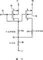
Figure 13 is the example circuit schematic diagram of the integrated device architecture shown in Figure 12 A-12C.
Embodiment
In following explanation, in order to provide, provided detail, for example material type, size, design feature, treatment step etc. to thorough of the present invention.But, those of ordinary skill in the art will understand, and implementing the present invention can not need these details.Should also be understood that the element among the figure is representational, proportionally do not draw for clarity.
Fig. 1 shows the example side cross-sectional view of vertical HVFET 10, and this HVFET 10 has such structure, and it comprises the extension drain region 12 of the N type silicon that is formed on the N+ doped silicon substrate 11.Substrate 11 is carried out heavy doping so that its resistance to the electric current of the drain electrode of flowing through minimizes, and drain electrode is positioned on the bottom of substrate in the device of finishing.In one embodiment, extend the part of drain region 12 for the epitaxial loayer of the top surface that extends to silicon wafer from substrate 11.Near top surface formation P this tagma 13 of type of epitaxial loayer and by p type island region territory 16 oss-divided N+ impure source district 14a and 14b.As can be seen, this tagma 13 of P type is arranged at and extends 12 tops, drain region and vertically will extend drain region 12 and N+ source area 14a and 14b and p type island region territory 16 separate.
In one embodiment, epitaxial loayer comprises that the doping content of the part of extending drain region 12 is linear gradients, shows the extension drain region of basic uniform electric field distribution with generation.Linear gradient can stop at certain the some place below the top surface of epitaxial loayer 12.
In the example vertical transistor of Fig. 1, extend platform or post 17 (two terms use as synonym in this application) that drain region 12, this tagma 13, source area 14a and 14b and p type island region territory 16 comprise silicon materials jointly.Fill the vertical trench on the opposite side that is formed at post 17 with dielectric material (for example oxide) layer, described dielectric material forms dielectric regions 15.Can require the height of decision post 17 and the spacing between width and the adjacent vertical trench by the puncture voltage of device.In each embodiment, the vertical height of platform 17 (thickness) is in about 30 μ m scope thick to 120 μ m.For example, be approximately the HVFET that forms on the tube core of 1mm * 1mm in size and can have the post 17 that vertical thickness is about 60 μ m.As another example, the transistor arrangement that forms on the tube core of about 2mm-4mm of each side can have the thick rod structure of about 30 μ m.In a particular embodiment, the transverse width of post 17 is too narrow to the degree (for example about 0.4 μ m is wide to 0.8 μ m) that can reliably make as far as possible, so that realize very high puncture voltage (for example 600-800V).
In another embodiment, be not that the transverse width of crossing over post 17 is arranged p type island region territory 16 (as shown in Figure 1) between N+ source area 14a and 14b, but the lateral length that can cross over post 17 alternately form N+ source area and p type island region territory at the top of post 17.In other words, the given sectional view shown in Fig. 1 will have the N+ source area 14 or the p type island region territory 16 of the whole transverse width extension of crossing over post 17, depend on where this cross section takes from.In such embodiments, each N+ source area 14 in both sides (along the lateral length of post) and p type island region territory 16 adjacency.Similarly, each p type island region territory 16 in both sides (along the lateral length of post) and N+ source area 14 adjacency.(shown in Figure 12 A and 12B that the example of such embodiment is discussed below).
The trench gate structure of vertical HVFET transistor 80 comprises grid element 18a, 18b, and each grid element is separately positioned between field plate 19a, 19b and this tagma 13, among the oxide areas 15a and 15b on the opposite side of post 17.High-quality (for example~500 approaching
 ) gate oxide level separates the sidewall of
 grid element 18 with the post 17 adjacent with this tagma 13.Grid element 18 can comprise polysilicon or certain other material of being fit to.In one embodiment, each grid element 18 has the degree of depth of transverse width and the about 3.5 μ m of about 1.5 μ m.
The personnel of putting into practice of this area will be understood that near the N+ source area 14 the top of post 17 and this tagma 13 of P-type all can be used common deposit, diffusion and/or inject treatment technology and be formed.After forming N+ source area 38, can finish HVFET 10 by the source, leakage, grid and the field plate electrode that utilize conventional manufacture method to form the respective regions/material (for clear not shown) that is electrically connected to device.
Fig. 2 A shows the example layout of the vertical HVFET structure shown in Fig. 1.The top view of Fig. 2 A shows single discrete HVFET, and it comprises upper crystal tube portion 30a and bottom transistor part 30b on the semiconductor element 21.By pseudo-silicon post 32 separately with these two parts.Each part 30 comprises a plurality of " runway (racetrack) " shape transistor arrangements or section, each transistor segments comprises elongate loop or ellipse, it is included in the silicon post 17 that opposite side is surrounded by dielectric regions 15a and 15b.Post 17 itself in the x and y direction horizontal expansion to form elongated continuously runway shape ring or oval.Be arranged among dielectric regions 15a and the 15b is corresponding grid element 18a and 18b and field plate 19a and 19b.Field plate 19a comprises single elongated member, and it ends in arbitrary end in circular finger tip (fingertip) zone.On the other hand, field plate 19b comprises elongate loop or the ellipse around post 17.(merged) that the field plate 19b of adjacent runway structure is illustrated as merging, thus they are shared in the common element of a side.As a reference, the sectional view of Fig. 1 can be taken from the line of cut A-A ' of the example layout of Fig. 2 A.
Should be appreciated that in the example of Fig. 2 A the width (be spacing) of each runway shape transistor segments on the y direction is approximately 13 μ m, the length on the x direction at about 400 μ m in the scope of 1000 μ m, and the post height is about 60 μ m.In other words, the length-width ratio of each runway shape transistor segments that comprises part 30a and 30b about 30 in 80 scope.In one embodiment, the length of each runway shape section is greater than at least 20 times of its spacing or width.
The personnel of putting into practice of this area will understand, and in the device architecture of finishing, use interconnect each silicon post 17 of each transistor segments of patterned metal layer.That is to say, in practical embodiments, respectively all source areas, grid element and field plate are routed to together electrode corresponding on the tube core.In illustrated embodiment, the transistor segments in each part 30 is crossed over the width of tube core 21 substantially and is arranged to side by side relationship along the y direction.Similarly, on the x direction, the extra length of the transistor segments of part 30a and 30b extends on the length of tube core 21 substantially.In the example layout of Fig. 2 A, cross over semiconductor element 21, separately the width of the dielectric regions 15 of silicon post and the width of field plate are uniform substantially.Arrange that with uniform width and spacing distance transistor segments has prevented to form space or hole after being used for the treatment step of layer that conformally deposit comprises dielectric regions 15 and field plate 19.
Fig. 2 B is the guide wire of alternative shape of the example layout shown in Fig. 2 A.For clarity, only show the post 17 and the dielectric regions 15b of each transistor segments.Illustrated pseudo-silicon post 32 separates the nose circle zone of the dielectric regions 15b of respective transistor section part 30a and 30b.In other words, the etched dark vertical trench that limits post 17 also limits pseudo-silicon post 32 in Semiconductor substrate.In one embodiment, make the width (be it separate transistor segments part) of pseudo-silicon post 32 on the x direction little to being made reliably.
Singulated dies HVFET is segmented into the stress elimination (stressrelief) that is in elongated runway shape transistor segments, to introduce (x direction) on the length direction by the purpose of pseudo-silicon post 32 divided portion.With the transistor device structures segmentation or be broken into two or more parts and alleviated the mechanical stress of crossing over tube core length.This stress is caused by the oxide areas that is positioned at the post side, and concentrates on the round nose place of each runway shape section usually.Thus by transistor device structures being segmented into two or more parts alleviate that mechanical stress has prevented the undesirable silicon post warpage that caused by stress and to the damage (for example dislocation) of silicon.
It being understood that stress that the layout by the height segmentation provides eliminate and the loss of conductive region between exist compromise.More segmentation causes bigger stress to alleviate, and is cost with the conductive region still.Usually, the vertical height of post is big more and semiconductor element is big more, and the number of transistor part that then needs or section is big more.In one embodiment, tube core for 2mm * 2mm with the high post of 60 μ m, the layout that utilization comprises four runway shape transistor part provides enough stress to alleviate in conducting resistance is about 1 ohm HVFET, described four runway shape transistor part are separated by pseudo-silicon post, and each pseudo-silicon post has the spacing (y direction) of about 13 μ m and the length (x direction) of about 450 μ m.
In another embodiment, not to be separated into right runway shape transistor segments with pseudo-silicon post, each is to being arranged in different piece, but can be with the pseudo-post that comprises different materials.The material that is used for pseudo-post should have near the thermal coefficient of expansion of silicon or fully be different from the thermal coefficient of expansion of thermal coefficient of expansion of dielectric regions so that alleviate stress on the length direction that is caused by the dielectric regions that is positioned at silicon post side.
Fig. 3 A shows another example layout of vertical HVFET structure shown in Figure 1.Fig. 3 B is the enlarged drawing of the part of the example layout shown in Fig. 3 A, only shows post 17, oxide areas 15b and optional pseudo-silicon post 33.Be similar to the embodiment of Fig. 2 A and 2B, Fig. 3 A and 3B show the single discrete HVFET on the semiconductor element 21, and it comprises upper crystal tube portion 30a and bottom transistor part 30b.But in the example of Fig. 3 A and 3B, dark vertical trench of being filled by oxide areas 15b and the field plate 19b of transistor part 30a and 30b are overlapping, are perhaps merged, and stay the pseudo-silicon post 33 of little rhombus between the transistor part of segmentation.In this embodiment, single pseudo-post is centered close between four round noses of adjacent paired transistor segments on two parts.Shown in example in, for the every N in the transistor part 30 that comprises tube core 21 (wherein N for greater than 1 integer) runway shape section or structure, have N-1 pseudo-post 33 altogether.
Fig. 4 A shows the another example layout of vertical HVFET structure shown in Figure 1.Fig. 4 B is the enlarged drawing of the part of the example layout shown in Fig. 4 A.In the enlarged drawing of Fig. 4 B for clear post 17 and the oxide areas 15b of only showing.In this example, the transistor segments that comprises HVFET of semiconductor element 21 is alternately moved half of length of each runway shape section, the result forms the runway shape transistor segments that alternately is associated with upper crystal tube portion 40a and bottom transistor part 40b.In other words, each transistor segments of the part 40a of delegation is separated by the pair of transistor section of part 40b, and this is arranged to concern end to end along the x direction to transistor segments.
It being understood that any percentage (fraction) that each section can be replaced mobile segment length.In other words, the section mobile be not limited to length 50% or half.Various embodiments can comprise the length that alternately moved transistor segments from greater than 0% to less than 100% any percentage or the section of percentage.
In the example of Fig. 4 A and 4B, the dielectric regions 15b of the transistor segments that replaces among appropriate section 40a and the 40b is merged.In illustrated specific embodiment, the round nose of the transistor segments that is associated with different adjacent parts is overlapping or merged, and makes that (along the x direction) merged in the each end for the field plate 19b of adjacent part.And the straight portion of the extension of the field plate 19b of the alternate transistors section of different piece is merged along the fundamental length of each section.It being understood that regional 15b and 19b can be merged under the situation that is with or without pseudo-post (or the pseudo-silicon post of isolating) between the appropriate section.
Fig. 5 shows the example layout of wafer 50, and it has the checkerboard type HVFET 10a-10d of tube core to tube core respectively on semiconductor element 21a-21d.Each of HVFET 10 comprises a plurality of runway shape transistor segments as shown in Figure 1, and they are arranged side by side square substantially piece along its width.In this example, HVFET 10a-10d includes length and crosses over the transistor segments that the length of respective dies 21a-21d is extended substantially.In one embodiment, the width of each section is about 13 μ m, and length at about 500 μ m in the scope of 2000 μ m.Other embodiment can have the length greater than 2000 μ m.The width that the piece of section or stacked structure are also crossed over each tube core substantially extends.(note the edge of scribe area between the square representative adjacent semiconductor tube core that the limit is arranged of each tube core 21.) though Fig. 5 shows two row and two HVFET 10 that are listed as, and is understandable that, can cross over the entire wafer substrate and repeat shown tube core to tube core checkerboard type and arrange.
In the example of Fig. 5, adjacent tube core is oriented as and makes the length of the transistor segments in the tube core extend in one direction in the row or column, and the length of the transistor segments in the adjacent tube core is extended along second orthogonal direction.For example, HVFET 10a is illustrated as the length of its transistor segments along x direction orientation, and adjacent HVFET 10b and 10c.Replace the orientation (being that checkerboard type is arranged) of the transistor segments in every singulated dies 21 orthogonally by crossing over wafer 50, will distribute along two orthogonal directions, reduced the warpage of wafer 50 thus by the mechanical stress that long dielectric regions produces.
Fig. 6 shows the tube core of the HVFET with segmentation another example layout to the wafer of tube core checkerboard type layout.The example of Fig. 6 has used the orientation of the method tube core identical with Fig. 5 to tube core ground alternate transistors structure; Yet, in the embodiment of Fig. 6, with the structural segmented one-tenth of HVFET a plurality of (for example two) part.For example, be segmented into two part 30a and the 30b that separates by pseudo-post 32 with crossing over each HVFET that the length of semiconductor element 21 and width extend substantially.
For square substantially tube core, each semiconductor element 21 shown in Fig. 6 has and identical layout shown in Figure 2.Be similar to the example shown in Fig. 5, adjacent tube core has crosses over the transistor segments that wafer 50 quadratures replace.That is to say that part 30a and the transistor segments among the 30b of tube core 21a and 21d have the length that is orientated on the x direction, and the part 30a of tube core 21b and 21c and the transistor segments among the 30b has the length that is orientated on the y direction.
Be appreciated that and for example form the HVFET of each tube core 21 with a plurality of transistor part of separating by one or more pseudo-posts greater than 2 transistor part.In addition, in the singulated dies layout with a plurality of transistor part shown in the example of Fig. 2 A-4B any one can be used in each tube core 21 shown in Fig. 6, and the orientation of each section is crossed over wafer 50 tube cores and is replaced to tube core ground.
Fig. 7 shows the example rectangular layout of tube core 25, and it has the checkerboard type piece of the runway shape HVFET section of piling up with basic square block that is arranged side by side or part 36.Adjacent part in the row or column is oriented to and makes the length of the transistor segments in the part extend in one direction, and the length of the transistor segments in other adjacent parts is extended on second orthogonal direction.For example, each row and column of tube core 25 comprises that being oriented to elongated transistor segments aims at the transistor part 36a of (aligned) and be oriented to the transistor part 36b that replaces that elongated transistor segments is aimed at along the y direction along the x direction.Space between transistor part 36a and the 36b comprises pseudo-silicon post; That is to say that the silicon that forms pseudo-post is not the active transistor zone.
In illustrated embodiment, tube core 25 comprises the transistor part 36 of triplex row and four row.Checkerboard type layout type shown in the example of Fig. 7 can be used for producing single discrete HVFET on the tube core of any (in feasible limit) rectilinear form almost.
Fig. 8 A is the top view of a part of example layout of incorporating the sensing fet of the vertical HVFET structure shown in Fig. 1 into.In an illustrated embodiment, sensing fet is integrated in the identical silicon post 17 as main Vertical power transistors device.Fig. 8 B is the side cross-sectional view by the line of cut A-A ' of the example layout shown in Fig. 8 A.Fig. 9 is the example circuit schematic diagram of the integrated device architecture shown in Fig. 8 A and the 8B.The overall observation, the top of post 17 seems to comprise lateral length alternating N+source area 14 and the P+ district 16 along the post in the given runway shape transistor segments.For example, from left to right, Fig. 8 A and 8B show regional 14a, 16a, 14b and the 16b of the top section that comprises vertical HVFET device 58 (see figure 9)s.This tagma 13 of P-extends to the top surface of post 17 the right to the next-door neighbour of regional 16b, thus regional 16b is separated with N+ zone 24, and it is associated with sensing fet device 59.
Should be appreciated that N+ zone 24 another cross side (to shown in the right of part) separate by the zone in this tagma 13 of P-on the surface that extends to post 17 alternating pattern similarly with corresponding N+/P+ regional 14 and 16.In typical embodiment, zone 24 comprises the fraction of whole transistor segments (post) layout, makes sensing fet 59 senses flow cross the fraction of the electric current of main vertical transistor devices 58.
In the example of Fig. 8 A and 8B, post 17 joins in relative cross side side with 18b by grid element 18a, and described grid element 18a and 18b separate with the top section of post 17 by gate oxide level 20a and 20b respectively.In source electrode 61 electric contact area 14 and 16 each, and the sensing electrode 62 N+ zone 24 of contact sensing fet 59 only.In a particular embodiment, source electrode 61 also can electrically contact inside and outside field plate element 19a and 19b.
Figure 10 A is the top view of a part of another example layout of incorporating the sensing fet of the vertical HVFET structure shown in Fig. 1 into.Figure 10 B is the side cross-sectional view by the line of cut B-B ' of sensing fet shown in Figure 10 A and HVFET.Figure 11 is the example circuit schematic diagram of the integrated device architecture shown in Figure 10 A and the 10B.Note the embodiment shown in Figure 10 A, the 10B and 11, sensing fet 69 comprises P+ zone 25 and the N+ zone 24 that replaces along the lateral length of post 17 (promptly around run-track shaped).Zone each in 24 and 25 is set among the 13b of this tagma of P-, and this tagma of described P-13b separates with this tagma of the P-13a that is associated with main vertical transistor 68 by the zone of the extension drain region 12 on the surface that extends to post 17.Among P-this tagma 13a and the 13b each extends to the surface at the post of two cross sides of the alternate sequence in the N+/P+ zone of respective transistor 68 and 69.
In Figure 11, vertical HVFET device 68 and sensing fet 69 are illustrated as sharing public grid 18 and public drain electrode node 63.Public extension drain region 64 and N+ substrate 65 are illustrated as being coupling in the resistor that is connected in series 64 and 65 between node 63 and the drain electrode 71 respectively.Source electrode 81 electrically contacts each in the zone 14 and 16 of main vertical transistor 68, and sensing electrode 82 zone 24 and 25 of contact sensing fet 69 only.Source electrode 81 also can electrically contact inside and outside field plate element 19a and the 19b in the metallization layout.
Figure 12 A is the top view of a part of another example layout of incorporating the sensing fet of the vertical HVFET structure shown in Fig. 1 into.Figure 12 B and 12C are respectively by the line of cut C-C ' of the device architecture shown in Figure 12 A and the side cross-sectional view of D-D '.Notice that in this embodiment, sensing fet is formed on the post that separates that is isolated from each other with main vertical HVFET device.Figure 12 B is the cross section of main vertical transistor devices 78 (being associated with post 17), and Figure 12 C is the cross section of sensing fet 79 (with post 17 ' be associated).As an example, post 17 ' can comprise the single runway shape transistor segments that is exclusively used in sensing fet 79, described single runway shape transistor segments is set to the contiguous transistor segments that is exclusively used in a plurality of other analogous shapes of main vertical transistor devices 78.Should be appreciated that main vertical HVFET device comprises the most transistor segments on the tube core, and sensing fet comprises minority (for example single one 's) transistor segments.
As shown in Figure 12B, main vertical transistor devices 78 comprises the alternately N+ zone 14 and the P+ zone 16 at the top that is arranged on post 17.In source electrode 91 electric contact area 14 and 16 each.In main transistor device 78, this tagma of P- 13a separation region 14 and 16 and extension drain region 12a below.Similarly, Figure 12 C illustrate comprise be arranged on post 17 ' the alternately N+ zone 24 at top and the sensing fet 79 in P+ zone 25.In sensing electrode 92 electric contact area 24 and 25 each.This tagma of P-13b separation region 24 and 25 and extension drain region 12b below.
Notice that in the example circuit schematic diagram of Figure 13 C, resistor 65 expressions are shown in the resistance of the N+ substrate 11 between common node 95 and the drain electrode 71.The resistance that extends drain region 12b is illustrated as being connected the drain electrode of sensing fet 79 and the resistor 64b between the node 95.Similarly, the resistance of extension drain region 12a is illustrated as being connected the drain electrode of main vertical transistor devices 78 and the resistor 64a between the common node 95.The equivalent circuit diagram of Figure 13 has reflected such fact: even sensing fet 79 and main transistor 78 are formed on the post separately, each post on semiconductor element is still shared public N+ area.
Though described above embodiment in conjunction with concrete type of device, those of ordinary skill in the art will understand multiple modification and change within the scope of the invention.For example, though described HVFET, illustrated method, layout and structure are equally applicable to other structures and type of device, comprise Schottky, diode, IGBT and bipolar structure.Therefore, specification and accompanying drawing should be regarded as and be exemplary and not restrictive.
Claims (24)
1. semiconductor device comprises:
Main vertical transistor, it comprises:
The substrate of first conduction type;
Be arranged on the semiconductor material pillar on the substrate, described post has width and along the length of first horizontal expansion, first source area comprises one or more zones of the top surface place that is arranged on described post or near first conduction type, this tagma of second conduction type is set in the post below first source area, and the extension drain region of first conduction type is set in the post below this tagma;
Be separately positioned on first and second dielectric regions of the opposite side of post, first dielectric regions is laterally surrounded by post, and second dielectric regions is laterally surrounded described post;
Be separately positioned on first and second field plates in first and second dielectric regions;
Be separately positioned on the top surface place of post in adjacent body district or first and second grid elements near first and second dielectric regions, described first and second grid elements distinguish by gate oxide and the body with first thickness;
Sensing transistor, it comprises:
Be arranged on the top surface place of post or near second source area of first conduction type, second source area laterally separates with first source area by the zone in this tagma of the top surface that extends to post along first,
The sensing transistor fraction of the electric current that flows that is used for sampling in main vertical transistor wherein.
2. semiconductor device according to claim 1, wherein said post are arranged to runway shape layout.
3. semiconductor device according to claim 1 further comprises:
Electrically contact the source electrode of described one or more first source areas;
Electrically contact the sensing source electrode of second source area; And
Electrically contact the drain electrode of the basal surface of substrate.
4. semiconductor device according to claim 1 further comprises the extension drain region in the post that is arranged on below this tagma.
5. semiconductor device according to claim 1, wherein along the first horizontal described length than at least 30 times greatly of described width.
6. semiconductor device according to claim 1, wherein first and second grid elements and first and second field plates insulation.
7. semiconductor device according to claim 1, wherein first source area further comprises one or more zones of the top surface place that is arranged on post or near second conduction type, and the one or more zones of this of first and second conduction types are along first adjacency that laterally is arranged so that in an alternating manner in these the one or more zones of each and second conduction type in these one or more zones of first conduction type.
8. semiconductor device comprises:
Main vertical field-effect transistor (FET); And
The sense field effect transistor, main vertical field-effect transistor and sense field effect transistor all are formed on the semiconductor material pillar on the substrate of first conduction type, described post has width and along the length of first horizontal expansion, first and second dielectric regions are arranged on the opposite side of post, first and second grid elements be provided with respectively contiguous in this tagma of post the top surface place or near first and second dielectric regions in post, main vertical field-effect transistor and sense field effect transistor are shared the extension drain region of first conduction type in the post that is formed on the substrate, and the first and second grid element ponds are shared by main vertical field-effect transistor and sense field effect transistor usually:
Main vertical field-effect transistor further comprises:
Be arranged on first this tagma of second conduction type in the post that extends on the drain region; And
Be arranged on the top surface place of post or near first source area, described source area by first this tagma with extend that the drain region is vertical to be separated;
The sense field effect transistor further comprises:
Be arranged on second this tagma of second conduction type in the post that extends on the drain region; And
Be arranged on the top surface place of post or near second source area, described second source area by second this tagma with extend that the drain region is vertical to be separated, second source area and first source area laterally separate and electric isolation along first,
The sense field effect transistor fraction of the electric current that flows that is used for sampling in main vertical field-effect transistor wherein.
9. semiconductor device according to claim 8 further comprises first and second field plates that are separately positioned in first and second dielectric regions.
10. semiconductor device according to claim 9 further comprises:
Electrically contact the source electrode of first source area;
Electrically contact the sensing source electrode of second source area; And
Electrically contact the drain electrode of the basal surface of substrate.
11. semiconductor device according to claim 10, wherein the source electrode also electrically contacts first and second field plates.
12. semiconductor device according to claim 8, the zone of wherein extending the drain region extends to the top surface of the post between first and second these tagmas.
13. semiconductor device according to claim 12, wherein first this tagma is along first top surface that extends transverse at the post of the opposite side of first source area, and second this tagma is along first top surface that extends transverse at the post of the opposite side of second source area.
14. semiconductor device according to claim 8, wherein first and second these tagmas are included as main vertical field-effect transistor and shared single this tagma of sense field effect transistor, and the zone in this single this tagma extends to the top surface of the post between first and second source areas.
15. semiconductor device according to claim 8, wherein said post are arranged to runway shape layout, the length of described post is bigger at least 30 times than width.
16. a semiconductor device comprises:
Be arranged to a plurality of transistor segments of side by side relationship, each transistor segments comprises:
On the substrate of first conduction type, form the semiconductor material pillar of runway shape layout, described post has along the length of first horizontal expansion and width, and described post has top surface place or near source area, extension drain region and this tagma that vertically separates source electrode and extend second conduction type of drain region that is arranged on post;
Be separately positioned on first and second dielectric regions of the opposite side of described post, first dielectric regions is laterally surrounded by post, and second dielectric regions is laterally surrounded described post;
Be separately positioned on the top surface place of post in adjacent body district or first and second grid elements near first and second dielectric regions;
Be separately positioned on first and second field plates in first and second dielectric regions;
Electrically contact the source electrode of the source area of most of transistor segments, this source electrode is associated with main vertical transistor:
Electrically contact the sensing electrode of the source area of minority transistor segments, this sensing electrode is associated with sensing transistor, be used for sampling in the main vertical transistor fraction of the electric current that flows of described sensing transistor; And
Electrically contact the drain electrode of the basal surface of substrate, this drain electrode and first and second grid elements are main vertical transistor and sensing transistor institute is shared.
17. semiconductor device according to claim 16, wherein said minority transistor segments comprises the single transistor section.
18. semiconductor device according to claim 16, wherein the source electrode electrically contacts first and second field plates of whole transistor segments.
19. semiconductor device according to claim 16, wherein the source electrode electrically contacts second field plate of whole transistor segments and first field plate of described most of transistor segments of being associated with main vertical transistor, and sensing electrode electrically contacts first field plate of the described minority transistor segments that is associated with sensing transistor.
20. semiconductor device according to claim 16, wherein along the first horizontal described length than at least 30 times greatly of described width.
21. semiconductor device according to claim 16, wherein first and second grid elements and first and second field plates insulation.
22. semiconductor device according to claim 16, wherein source area comprises first district of first conduction type and second district of second conduction type, and first and second districts are along one in first each adjacency second district that laterally is arranged so that in an alternating manner in first district.
23. according to each described semiconductor device in the claim 1 to 7, wherein said first source area comprises the alternating pattern in each N+/P+ zone.
24. each described semiconductor device in 15 according to Claim 8, wherein said first source area and described second source area comprise the alternate sequence in N+/P+ zone respectively.
Priority Applications (1)
| Application Number | Priority Date | Filing Date | Title |
|---|---|---|---|
| CN201110349590.5A CN102376768B (en) | 2007-02-16 | 2008-02-18 | With the sensing FET that high-voltage vertical transistor is integrated |
Applications Claiming Priority (2)
| Application Number | Priority Date | Filing Date | Title |
|---|---|---|---|
| US11/707,586 US8653583B2 (en) | 2007-02-16 | 2007-02-16 | Sensing FET integrated with a high-voltage transistor |
| US11/707586 | 2007-02-16 |
Related Child Applications (1)
| Application Number | Title | Priority Date | Filing Date |
|---|---|---|---|
| CN201110349590.5A Division CN102376768B (en) | 2007-02-16 | 2008-02-18 | With the sensing FET that high-voltage vertical transistor is integrated |
Publications (2)
| Publication Number | Publication Date |
|---|---|
| CN101246887A CN101246887A (en) | 2008-08-20 |
| CN101246887B true CN101246887B (en) | 2011-12-21 |
Family
ID=39410363
Family Applications (2)
| Application Number | Title | Priority Date | Filing Date |
|---|---|---|---|
| CN2008100807528A Active CN101246887B (en) | 2007-02-16 | 2008-02-18 | Sensing FET integrated with a high-voltage vertical transistor |
| CN201110349590.5A Active CN102376768B (en) | 2007-02-16 | 2008-02-18 | With the sensing FET that high-voltage vertical transistor is integrated |
Family Applications After (1)
| Application Number | Title | Priority Date | Filing Date |
|---|---|---|---|
| CN201110349590.5A Active CN102376768B (en) | 2007-02-16 | 2008-02-18 | With the sensing FET that high-voltage vertical transistor is integrated |
Country Status (4)
| Country | Link |
|---|---|
| US (1) | US8653583B2 (en) |
| EP (1) | EP1959499A3 (en) |
| JP (2) | JP5214288B2 (en) |
| CN (2) | CN101246887B (en) |
Families Citing this family (29)
| Publication number | Priority date | Publication date | Assignee | Title |
|---|---|---|---|---|
| DE102005051417A1 (en) * | 2005-10-27 | 2007-05-03 | X-Fab Semiconductor Foundries Ag | Simulation or layout method for vertical power transistors with variable channel width and variable gate-drain capacitance |
| US8093621B2 (en) * | 2008-12-23 | 2012-01-10 | Power Integrations, Inc. | VTS insulated gate bipolar transistor |
| US7595523B2 (en) | 2007-02-16 | 2009-09-29 | Power Integrations, Inc. | Gate pullback at ends of high-voltage vertical transistor structure |
| US8653583B2 (en) | 2007-02-16 | 2014-02-18 | Power Integrations, Inc. | Sensing FET integrated with a high-voltage transistor |
| US7557406B2 (en) * | 2007-02-16 | 2009-07-07 | Power Integrations, Inc. | Segmented pillar layout for a high-voltage vertical transistor |
| US7859037B2 (en) * | 2007-02-16 | 2010-12-28 | Power Integrations, Inc. | Checkerboarded high-voltage vertical transistor layout |
| US7468536B2 (en) * | 2007-02-16 | 2008-12-23 | Power Integrations, Inc. | Gate metal routing for transistor with checkerboarded layout |
| US8674434B2 (en) * | 2008-03-24 | 2014-03-18 | Micron Technology, Inc. | Impact ionization devices |
| US7964912B2 (en) | 2008-09-18 | 2011-06-21 | Power Integrations, Inc. | High-voltage vertical transistor with a varied width silicon pillar |
| US7871882B2 (en) * | 2008-12-20 | 2011-01-18 | Power Integrations, Inc. | Method of fabricating a deep trench insulated gate bipolar transistor |
| US20100155831A1 (en) * | 2008-12-20 | 2010-06-24 | Power Integrations, Inc. | Deep trench insulated gate bipolar transistor |
| US8796760B2 (en) * | 2012-03-14 | 2014-08-05 | Taiwan Semiconductor Manufacturing Company, Ltd. | Transistor and method of manufacturing the same |
| US8653600B2 (en) | 2012-06-01 | 2014-02-18 | Power Integrations, Inc. | High-voltage monolithic schottky device structure |
| US9136368B2 (en) * | 2013-10-03 | 2015-09-15 | Texas Instruments Incorporated | Trench gate trench field plate semi-vertical semi-lateral MOSFET |
| US10325988B2 (en) | 2013-12-13 | 2019-06-18 | Power Integrations, Inc. | Vertical transistor device structure with cylindrically-shaped field plates |
| US9543396B2 (en) | 2013-12-13 | 2017-01-10 | Power Integrations, Inc. | Vertical transistor device structure with cylindrically-shaped regions |
| US9461639B2 (en) * | 2014-05-16 | 2016-10-04 | Freescale Semiconductor, Inc. | Semiconductor device and power circuit including a sense transistor for current sensing |
| US9496339B2 (en) * | 2014-06-02 | 2016-11-15 | Infineon Technologies Austria Ag | Semiconductor device comprising trench structures |
| KR102026543B1 (en) * | 2014-08-19 | 2019-09-27 | 비쉐이-실리코닉스 | Electronic circuit |
| US9973183B2 (en) | 2015-09-28 | 2018-05-15 | Power Integrations, Inc. | Field-effect transistor device with partial finger current sensing FETs |
| US9983239B2 (en) | 2016-05-13 | 2018-05-29 | Power Integrations, Inc. | Integrated linear current sense circuitry for semiconductor transistor devices |
| WO2018030990A1 (en) | 2016-08-08 | 2018-02-15 | Power Integrations, Inc. | Integrated circuit fast temperature sensing of a semiconductor switching device |
| DE102016125879B3 (en) * | 2016-12-29 | 2018-06-21 | Infineon Technologies Ag | A semiconductor device having an IGBT region and a non-switchable diode region |
| US10753964B2 (en) * | 2017-04-27 | 2020-08-25 | Microchip Technology Incorporated | Current sensing for integrated circuit devices |
| JP7224979B2 (en) | 2019-03-15 | 2023-02-20 | 株式会社東芝 | semiconductor equipment |
| US11004970B2 (en) * | 2019-05-20 | 2021-05-11 | Nxp Usa, Inc. | Mirror device structure for power MOSFET and method of manufacture |
| JP7186679B2 (en) | 2019-08-23 | 2022-12-09 | 三菱電機株式会社 | digital output device |
| US11322612B2 (en) | 2019-09-17 | 2022-05-03 | Kabushiki Kaisha Toshiba | Semiconductor device with region of varying thickness |
| DE102019128071B3 (en) * | 2019-10-17 | 2021-02-04 | Infineon Technologies Ag | TRANSISTOR COMPONENT |
Citations (3)
| Publication number | Priority date | Publication date | Assignee | Title |
|---|---|---|---|---|
| US4951102A (en) * | 1988-08-24 | 1990-08-21 | Harris Corporation | Trench gate VCMOS |
| US5821580A (en) * | 1996-04-30 | 1998-10-13 | Kabushiki Kaisha Toshiba | MOS device having a trench gate structure |
| EP1689001A2 (en) * | 2005-02-03 | 2006-08-09 | Power Integrations, Inc. | High-voltage semiconductor devices |
Family Cites Families (181)
| Publication number | Priority date | Publication date | Assignee | Title |
|---|---|---|---|---|
| US4343015A (en) | 1980-05-14 | 1982-08-03 | General Electric Company | Vertical channel field effect transistor |
| GB2089119A (en) * | 1980-12-10 | 1982-06-16 | Philips Electronic Associated | High voltage semiconductor devices |
| US4626879A (en) | 1982-12-21 | 1986-12-02 | North American Philips Corporation | Lateral double-diffused MOS transistor devices suitable for source-follower applications |
| US4738936A (en) * | 1983-07-01 | 1988-04-19 | Acrian, Inc. | Method of fabrication lateral FET structure having a substrate to source contact |
| US4626789A (en) | 1983-08-19 | 1986-12-02 | Hitachi, Ltd. | Demodulating circuit for data signal |
| US4531173A (en) | 1983-11-02 | 1985-07-23 | Motorola, Inc. | Protective power foldback circuit for a power semiconductor |
| US4553084A (en) * | 1984-04-02 | 1985-11-12 | Motorola, Inc. | Current sensing circuit |
| US4618541A (en) | 1984-12-21 | 1986-10-21 | Advanced Micro Devices, Inc. | Method of forming a silicon nitride film transparent to ultraviolet radiation and resulting article |
| JPS61168253A (en) * | 1985-01-19 | 1986-07-29 | Sharp Corp | High withstand voltage mos field effect semiconductor device |
| US4665426A (en) * | 1985-02-01 | 1987-05-12 | Advanced Micro Devices, Inc. | EPROM with ultraviolet radiation transparent silicon nitride passivation layer |
| US4963951A (en) | 1985-11-29 | 1990-10-16 | General Electric Company | Lateral insulated gate bipolar transistors with improved latch-up immunity |
| US4764800A (en) | 1986-05-07 | 1988-08-16 | Advanced Micro Devices, Inc. | Seal structure for an integrated circuit |
| US4769685A (en) | 1986-10-27 | 1988-09-06 | General Motors Corporation | Recessed-gate junction-MOS field effect transistor |
| US4796070A (en) * | 1987-01-15 | 1989-01-03 | General Electric Company | Lateral charge control semiconductor device and method of fabrication |
| US5010024A (en) * | 1987-03-04 | 1991-04-23 | Advanced Micro Devices, Inc. | Passivation for integrated circuit structures |
| US4811075A (en) * | 1987-04-24 | 1989-03-07 | Power Integrations, Inc. | High voltage MOS transistors |
| US4890144A (en) | 1987-09-14 | 1989-12-26 | Motorola, Inc. | Integrated circuit trench cell |
| JPH01112764A (en) | 1987-10-27 | 1989-05-01 | Nec Corp | Semiconductor device |
| US4926074A (en) * | 1987-10-30 | 1990-05-15 | North American Philips Corporation | Semiconductor switch with parallel lateral double diffused MOS transistor and lateral insulated gate transistor |
| US4939566A (en) | 1987-10-30 | 1990-07-03 | North American Philips Corporation | Semiconductor switch with parallel DMOS and IGT |
| US4890146A (en) | 1987-12-16 | 1989-12-26 | Siliconix Incorporated | High voltage level shift semiconductor device |
| US4922327A (en) * | 1987-12-24 | 1990-05-01 | University Of Toronto Innovations Foundation | Semiconductor LDMOS device with upper and lower passages |
| US4929987A (en) * | 1988-02-01 | 1990-05-29 | General Instrument Corporation | Method for setting the threshold voltage of a power mosfet |
| US5025296A (en) * | 1988-02-29 | 1991-06-18 | Motorola, Inc. | Center tapped FET |
| JPH0777262B2 (en) * | 1988-04-19 | 1995-08-16 | 日本電気株式会社 | Vertical field effect transistor |
| US5283201A (en) | 1988-05-17 | 1994-02-01 | Advanced Power Technology, Inc. | High density power device fabrication process |
| US5237193A (en) | 1988-06-24 | 1993-08-17 | Siliconix Incorporated | Lightly doped drain MOSFET with reduced on-resistance |
| DE68926384T2 (en) | 1988-11-29 | 1996-10-10 | Toshiba Kawasaki Kk | Lateral conductivity modulation MOSFET |
| US5072266A (en) | 1988-12-27 | 1991-12-10 | Siliconix Incorporated | Trench DMOS power transistor with field-shaping body profile and three-dimensional geometry |
| US5008794A (en) * | 1989-12-21 | 1991-04-16 | Power Integrations, Inc. | Regulated flyback converter with spike suppressing coupled inductors |
| JP2597412B2 (en) | 1990-03-20 | 1997-04-09 | 三菱電機株式会社 | Semiconductor device and manufacturing method thereof |
| US5040045A (en) | 1990-05-17 | 1991-08-13 | U.S. Philips Corporation | High voltage MOS transistor having shielded crossover path for a high voltage connection bus |
| US5072268A (en) | 1991-03-12 | 1991-12-10 | Power Integrations, Inc. | MOS gated bipolar transistor |
| US5122848A (en) * | 1991-04-08 | 1992-06-16 | Micron Technology, Inc. | Insulated-gate vertical field-effect transistor with high current drive and minimum overlap capacitance |
| US5386136A (en) * | 1991-05-06 | 1995-01-31 | Siliconix Incorporated | Lightly-doped drain MOSFET with improved breakdown characteristics |
| US5146298A (en) | 1991-08-16 | 1992-09-08 | Eklund Klas H | Device which functions as a lateral double-diffused insulated gate field effect transistor or as a bipolar transistor |
| US5164891A (en) | 1991-08-21 | 1992-11-17 | Power Integrations, Inc. | Low noise voltage regulator and method using a gated single ended oscillator |
| US5258636A (en) | 1991-12-12 | 1993-11-02 | Power Integrations, Inc. | Narrow radius tips for high voltage semiconductor devices with interdigitated source and drain electrodes |
| US5270264A (en) | 1991-12-20 | 1993-12-14 | Intel Corporation | Process for filling submicron spaces with dielectric |
| US5285367A (en) * | 1992-02-07 | 1994-02-08 | Power Integrations, Inc. | Linear load circuit to control switching power supplies under minimum load conditions |
| JP3435173B2 (en) | 1992-07-10 | 2003-08-11 | 株式会社日立製作所 | Semiconductor device |
| US5294824A (en) * | 1992-07-31 | 1994-03-15 | Motorola, Inc. | High voltage transistor having reduced on-resistance |
| US5323044A (en) * | 1992-10-02 | 1994-06-21 | Power Integrations, Inc. | Bi-directional MOSFET switch |
| US5326711A (en) | 1993-01-04 | 1994-07-05 | Texas Instruments Incorporated | High performance high voltage vertical transistor and method of fabrication |
| US5408141A (en) * | 1993-01-04 | 1995-04-18 | Texas Instruments Incorporated | Sensed current driving device |
| US5274259A (en) * | 1993-02-01 | 1993-12-28 | Power Integrations, Inc. | High voltage transistor |
| US5313082A (en) * | 1993-02-16 | 1994-05-17 | Power Integrations, Inc. | High voltage MOS transistor with a low on-resistance |
| DE4309764C2 (en) | 1993-03-25 | 1997-01-30 | Siemens Ag | Power MOSFET |
| US5349225A (en) | 1993-04-12 | 1994-09-20 | Texas Instruments Incorporated | Field effect transistor with a lightly doped drain |
| US5324683A (en) * | 1993-06-02 | 1994-06-28 | Motorola, Inc. | Method of forming a semiconductor structure having an air region |
| BE1007283A3 (en) | 1993-07-12 | 1995-05-09 | Philips Electronics Nv | Semiconductor device with most with an extended drain area high voltage. |
| DE69322963T2 (en) | 1993-09-17 | 1999-06-24 | Cons Ric Microelettronica | An integrated device with a bipolar transistor and a MOSFET transistor in an emitter circuit arrangement |
| US5523604A (en) | 1994-05-13 | 1996-06-04 | International Rectifier Corporation | Amorphous silicon layer for top surface of semiconductor device |
| US5494853A (en) | 1994-07-25 | 1996-02-27 | United Microelectronics Corporation | Method to solve holes in passivation by metal layout |
| JP3338185B2 (en) * | 1994-08-02 | 2002-10-28 | 株式会社東芝 | Semiconductor device |
| US5521105A (en) * | 1994-08-12 | 1996-05-28 | United Microelectronics Corporation | Method of forming counter-doped island in power MOSFET |
| JP3959125B2 (en) * | 1994-09-14 | 2007-08-15 | 株式会社東芝 | Semiconductor device |
| US5550405A (en) | 1994-12-21 | 1996-08-27 | Advanced Micro Devices, Incorporated | Processing techniques for achieving production-worthy, low dielectric, low interconnect resistance and high performance ICS |
| US5656543A (en) | 1995-02-03 | 1997-08-12 | National Semiconductor Corporation | Fabrication of integrated circuits with borderless vias |
| EP0726603B1 (en) * | 1995-02-10 | 1999-04-21 | SILICONIX Incorporated | Trenched field effect transistor with PN depletion barrier |
| US5670828A (en) | 1995-02-21 | 1997-09-23 | Advanced Micro Devices, Inc. | Tunneling technology for reducing intra-conductive layer capacitance |
| JP3291958B2 (en) * | 1995-02-21 | 2002-06-17 | 富士電機株式会社 | Back source MOSFET |
| US6049108A (en) | 1995-06-02 | 2000-04-11 | Siliconix Incorporated | Trench-gated MOSFET with bidirectional voltage clamping |
| US6204533B1 (en) | 1995-06-02 | 2001-03-20 | Siliconix Incorporated | Vertical trench-gated power MOSFET having stripe geometry and high cell density |
| US5659201A (en) | 1995-06-05 | 1997-08-19 | Advanced Micro Devices, Inc. | High conductivity interconnection line |
| KR100188096B1 (en) * | 1995-09-14 | 1999-06-01 | 김광호 | Semiconductor device and manufacturing method of the same |
| US5637898A (en) * | 1995-12-22 | 1997-06-10 | North Carolina State University | Vertical field effect transistors having improved breakdown voltage capability and low on-state resistance |
| US6097063A (en) | 1996-01-22 | 2000-08-01 | Fuji Electric Co., Ltd. | Semiconductor device having a plurality of parallel drift regions |
| US6184555B1 (en) * | 1996-02-05 | 2001-02-06 | Siemens Aktiengesellschaft | Field effect-controlled semiconductor component |
| DE19611045C1 (en) | 1996-03-20 | 1997-05-22 | Siemens Ag | Field effect transistor e.g. vertical MOS type |
| JP2000515684A (en) | 1996-07-19 | 2000-11-21 | シリコニックス・インコーポレイテッド | High density trench DMOS transistor with trench bottom implant region |
| US5841166A (en) | 1996-09-10 | 1998-11-24 | Spectrian, Inc. | Lateral DMOS transistor for RF/microwave applications |
| JP3504085B2 (en) * | 1996-09-30 | 2004-03-08 | 株式会社東芝 | Semiconductor device |
| US6168983B1 (en) * | 1996-11-05 | 2001-01-02 | Power Integrations, Inc. | Method of making a high-voltage transistor with multiple lateral conduction layers |
| US6207994B1 (en) | 1996-11-05 | 2001-03-27 | Power Integrations, Inc. | High-voltage transistor with multi-layer conduction region |
| US6639277B2 (en) | 1996-11-05 | 2003-10-28 | Power Integrations, Inc. | High-voltage transistor with multi-layer conduction region |
| KR100228331B1 (en) * | 1996-12-30 | 1999-11-01 | 김영환 | Method for manufacturing triple well of semiconductor device |
| EP0856887B1 (en) | 1997-01-31 | 2004-04-28 | SGS-THOMSON MICROELECTRONICS S.r.l. | Process for forming a morphological edge structure to seal integrated electronic devices, and corresponding device |
| JP3393544B2 (en) | 1997-02-26 | 2003-04-07 | シャープ株式会社 | Method for manufacturing semiconductor device |
| US6133607A (en) | 1997-05-22 | 2000-10-17 | Kabushiki Kaisha Toshiba | Semiconductor device |
| US5869875A (en) * | 1997-06-10 | 1999-02-09 | Spectrian | Lateral diffused MOS transistor with trench source contact |
| US6054752A (en) * | 1997-06-30 | 2000-04-25 | Denso Corporation | Semiconductor device |
| US6194283B1 (en) * | 1997-10-29 | 2001-02-27 | Advanced Micro Devices, Inc. | High density trench fill due to new spacer fill method including isotropically etching silicon nitride spacers |
| US6316807B1 (en) | 1997-12-05 | 2001-11-13 | Naoto Fujishima | Low on-resistance trench lateral MISFET with better switching characteristics and method for manufacturing same |
| JP3410949B2 (en) * | 1998-02-12 | 2003-05-26 | 株式会社東芝 | Semiconductor device |
| US6362064B2 (en) * | 1998-04-21 | 2002-03-26 | National Semiconductor Corporation | Elimination of walkout in high voltage trench isolated devices |
| JP3211771B2 (en) | 1998-05-26 | 2001-09-25 | 日本電気株式会社 | Voice transceiver |
| JP3016762B2 (en) | 1998-06-25 | 2000-03-06 | 松下電子工業株式会社 | Semiconductor device and manufacturing method thereof |
| US6037631A (en) | 1998-09-18 | 2000-03-14 | Siemens Aktiengesellschaft | Semiconductor component with a high-voltage endurance edge structure |
| US5998833A (en) * | 1998-10-26 | 1999-12-07 | North Carolina State University | Power semiconductor devices having improved high frequency switching and breakdown characteristics |
| US6621121B2 (en) | 1998-10-26 | 2003-09-16 | Silicon Semiconductor Corporation | Vertical MOSFETs having trench-based gate electrodes within deeper trench-based source electrodes |
| US6674107B1 (en) * | 1998-12-07 | 2004-01-06 | Lovoltech, Inc. | Enhancement mode junction field effect transistor with low on resistance |
| US6304007B1 (en) | 1998-12-09 | 2001-10-16 | Lovoltech, Inc. | Switcher for switching capacitors |
| US6307223B1 (en) | 1998-12-11 | 2001-10-23 | Lovoltech, Inc. | Complementary junction field effect transistors |
| US6281705B1 (en) * | 1998-12-11 | 2001-08-28 | Lovoltech, Inc. | Power supply module in integrated circuits |
| US6251716B1 (en) | 1999-01-06 | 2001-06-26 | Lovoltech, Inc. | JFET structure and manufacture method for low on-resistance and low voltage application |
| US6084277A (en) | 1999-02-18 | 2000-07-04 | Power Integrations, Inc. | Lateral power MOSFET with improved gate design |
| JP2000252465A (en) | 1999-03-03 | 2000-09-14 | Sony Corp | Semiconductor device and manufacture thereof |
| US6191447B1 (en) * | 1999-05-28 | 2001-02-20 | Micro-Ohm Corporation | Power semiconductor devices that utilize tapered trench-based insulating regions to improve electric field profiles in highly doped drift region mesas and methods of forming same |
| GB9917099D0 (en) * | 1999-07-22 | 1999-09-22 | Koninkl Philips Electronics Nv | Cellular trench-gate field-effect transistors |
| JP3971062B2 (en) | 1999-07-29 | 2007-09-05 | 株式会社東芝 | High voltage semiconductor device |
| US6365932B1 (en) * | 1999-08-20 | 2002-04-02 | Denso Corporation | Power MOS transistor |
| US6127703A (en) | 1999-08-31 | 2000-10-03 | Philips Electronics North America Corporation | Lateral thin-film silicon-on-insulator (SOI) PMOS device having a drain extension region |
| US6614289B1 (en) | 2000-11-07 | 2003-09-02 | Lovoltech Inc. | Starter device for normally off FETs |
| US6580252B1 (en) | 1999-10-29 | 2003-06-17 | Lovoltech, Inc. | Boost circuit with normally off JFET |
| US6355513B1 (en) * | 1999-10-29 | 2002-03-12 | Lovoltech, Inc. | Asymmetric depletion region for normally off JFET |
| US6566936B1 (en) * | 1999-10-29 | 2003-05-20 | Lovoltech Inc. | Two terminal rectifier normally OFF JFET |
| US6734715B1 (en) * | 1999-11-29 | 2004-05-11 | Lovoltech, Inc. | Two terminal rectifier using normally off JFET |
| US6349047B1 (en) * | 2000-12-18 | 2002-02-19 | Lovoltech, Inc. | Full wave rectifier circuit using normally off JFETs |
| US6489653B2 (en) | 1999-12-27 | 2002-12-03 | Kabushiki Kaisha Toshiba | Lateral high-breakdown-voltage transistor |
| GB0003185D0 (en) | 2000-02-12 | 2000-04-05 | Koninkl Philips Electronics Nv | An insulated gate field effect device |
| US7098634B1 (en) | 2003-02-21 | 2006-08-29 | Lovoltech, Inc. | Buck-boost circuit with normally off JFET |
| US6781194B2 (en) | 2001-04-11 | 2004-08-24 | Silicon Semiconductor Corporation | Vertical power devices having retrograded-doped transition regions and insulated trench-based electrodes therein |
| JP3448015B2 (en) | 2000-07-26 | 2003-09-16 | 松下電器産業株式会社 | Semiconductor device and manufacturing method thereof |
| US6750698B1 (en) | 2000-09-29 | 2004-06-15 | Lovoltech, Inc. | Cascade circuits utilizing normally-off junction field effect transistors for low on-resistance and low voltage applications |
| CA2360031C (en) * | 2000-10-30 | 2006-06-20 | Thomas & Betts International, Inc. | Capacitive test point voltage and phasing detector |
| US6653691B2 (en) * | 2000-11-16 | 2003-11-25 | Silicon Semiconductor Corporation | Radio frequency (RF) power devices having faraday shield layers therein |
| US6468847B1 (en) | 2000-11-27 | 2002-10-22 | Power Integrations, Inc. | Method of fabricating a high-voltage transistor |
| US6509220B2 (en) * | 2000-11-27 | 2003-01-21 | Power Integrations, Inc. | Method of fabricating a high-voltage transistor |
| US6768171B2 (en) | 2000-11-27 | 2004-07-27 | Power Integrations, Inc. | High-voltage transistor with JFET conduction channels |
| US6424007B1 (en) * | 2001-01-24 | 2002-07-23 | Power Integrations, Inc. | High-voltage transistor with buried conduction layer |
| US6677641B2 (en) | 2001-10-17 | 2004-01-13 | Fairchild Semiconductor Corporation | Semiconductor structure with improved smaller forward voltage loss and higher blocking capability |
| US7345342B2 (en) * | 2001-01-30 | 2008-03-18 | Fairchild Semiconductor Corporation | Power semiconductor devices and methods of manufacture |
| US6356059B1 (en) * | 2001-02-16 | 2002-03-12 | Lovoltech, Inc. | Buck converter with normally off JFET |
| US6683346B2 (en) * | 2001-03-09 | 2004-01-27 | Fairchild Semiconductor Corporation | Ultra dense trench-gated power-device with the reduced drain-source feedback capacitance and Miller charge |
| US6528880B1 (en) * | 2001-06-25 | 2003-03-04 | Lovoltech Inc. | Semiconductor package for power JFET having copper plate for source and ribbon contact for gate |
| JP4421144B2 (en) | 2001-06-29 | 2010-02-24 | 株式会社東芝 | Semiconductor device |
| US7221011B2 (en) | 2001-09-07 | 2007-05-22 | Power Integrations, Inc. | High-voltage vertical transistor with a multi-gradient drain doping profile |
| US6573558B2 (en) * | 2001-09-07 | 2003-06-03 | Power Integrations, Inc. | High-voltage vertical transistor with a multi-layered extended drain structure |
| US6555873B2 (en) * | 2001-09-07 | 2003-04-29 | Power Integrations, Inc. | High-voltage lateral transistor with a multi-layered extended drain structure |
| US6683344B2 (en) * | 2001-09-07 | 2004-01-27 | Ixys Corporation | Rugged and fast power MOSFET and IGBT |
| US6635544B2 (en) | 2001-09-07 | 2003-10-21 | Power Intergrations, Inc. | Method of fabricating a high-voltage transistor with a multi-layered extended drain structure |
| US6555883B1 (en) * | 2001-10-29 | 2003-04-29 | Power Integrations, Inc. | Lateral power MOSFET for high switching speeds |
| US6552597B1 (en) * | 2001-11-02 | 2003-04-22 | Power Integrations, Inc. | Integrated circuit with closely coupled high voltage output and offline transistor pair |
| DE10214151B4 (en) | 2002-03-28 | 2007-04-05 | Infineon Technologies Ag | Semiconductor device with increased breakdown voltage in the edge region |
| US6900506B1 (en) * | 2002-04-04 | 2005-05-31 | Lovoltech, Inc. | Method and structure for a high voltage junction field effect transistor |
| JP4107867B2 (en) | 2002-04-09 | 2008-06-25 | 株式会社ミツカングループ本社 | Citrus seasoning with packaging |
| US6583663B1 (en) * | 2002-04-22 | 2003-06-24 | Power Integrations, Inc. | Power integrated circuit with distributed gate driver |
| JP4107877B2 (en) | 2002-05-16 | 2008-06-25 | セイコーインスツル株式会社 | Semiconductor nonvolatile memory device |
| US7262461B1 (en) | 2002-05-20 | 2007-08-28 | Qspeed Semiconductor Inc. | JFET and MESFET structures for low voltage, high current and high frequency applications |
| US6921932B1 (en) * | 2002-05-20 | 2005-07-26 | Lovoltech, Inc. | JFET and MESFET structures for low voltage, high current and high frequency applications |
| US7268378B1 (en) | 2002-05-29 | 2007-09-11 | Qspeed Semiconductor Inc. | Structure for reduced gate capacitance in a JFET |
| JP2004022700A (en) | 2002-06-14 | 2004-01-22 | Sanyo Electric Co Ltd | Semiconductor device |
| US6777722B1 (en) * | 2002-07-02 | 2004-08-17 | Lovoltech, Inc. | Method and structure for double dose gate in a JFET |
| US6661276B1 (en) | 2002-07-29 | 2003-12-09 | Lovoltech Inc. | MOSFET driver matching circuit for an enhancement mode JFET |
| US6747342B1 (en) | 2002-08-09 | 2004-06-08 | Lovoltech, Inc. | Flip-chip packaging |
| JP4158453B2 (en) | 2002-08-22 | 2008-10-01 | 株式会社デンソー | Semiconductor device and manufacturing method thereof |
| US6696706B1 (en) * | 2002-10-22 | 2004-02-24 | Lovoltech, Inc. | Structure and method for a junction field effect transistor with reduced gate capacitance |
| US6774417B1 (en) | 2002-10-23 | 2004-08-10 | Lovoltech, Inc. | Electrostatic discharge protection device for integrated circuits |
| US7075132B1 (en) * | 2002-12-30 | 2006-07-11 | Lovoltech, Inc. | Programmable junction field effect transistor and method for programming the same |
| US7452763B1 (en) | 2003-03-04 | 2008-11-18 | Qspeed Semiconductor Inc. | Method for a junction field effect transistor with reduced gate capacitance |
| US7009228B1 (en) * | 2003-03-04 | 2006-03-07 | Lovoltech, Incorporated | Guard ring structure and method for fabricating same |
| US7038260B1 (en) * | 2003-03-04 | 2006-05-02 | Lovoltech, Incorporated | Dual gate structure for a FET and method for fabricating same |
| US6887768B1 (en) * | 2003-05-15 | 2005-05-03 | Lovoltech, Inc. | Method and structure for composite trench fill |
| US6865093B2 (en) * | 2003-05-27 | 2005-03-08 | Power Integrations, Inc. | Electronic circuit control element with tap element |
| US7227242B1 (en) | 2003-10-09 | 2007-06-05 | Qspeed Semiconductor Inc. | Structure and method for enhanced performance in semiconductor substrates |
| US7157959B2 (en) * | 2004-03-31 | 2007-01-02 | Semiconductor Components Industries, L.L.C. | Method of forming a self-gated transistor and structure therefor |
| US7211845B1 (en) * | 2004-04-19 | 2007-05-01 | Qspeed Semiconductor, Inc. | Multiple doped channel in a multiple doped gate junction field effect transistor |
| US7608888B1 (en) | 2004-06-10 | 2009-10-27 | Qspeed Semiconductor Inc. | Field effect transistor |
| US7417266B1 (en) | 2004-06-10 | 2008-08-26 | Qspeed Semiconductor Inc. | MOSFET having a JFET embedded as a body diode |
| US7238976B1 (en) * | 2004-06-15 | 2007-07-03 | Qspeed Semiconductor Inc. | Schottky barrier rectifier and method of manufacturing the same |
| US7135748B2 (en) | 2004-10-26 | 2006-11-14 | Power Integrations, Inc. | Integrated circuit with multi-length output transistor segment |
| US20060086974A1 (en) | 2004-10-26 | 2006-04-27 | Power Integrations, Inc. | Integrated circuit with multi-length power transistor segments |
| US7436039B2 (en) * | 2005-01-06 | 2008-10-14 | Velox Semiconductor Corporation | Gallium nitride semiconductor device |
| US7348826B1 (en) * | 2005-03-18 | 2008-03-25 | Qspeed Semiconductor Inc. | Composite field effect transistor |
| US7696598B2 (en) * | 2005-12-27 | 2010-04-13 | Qspeed Semiconductor Inc. | Ultrafast recovery diode |
| CN101361194B (en) * | 2005-12-27 | 2010-12-22 | 美商科斯德半导体股份有限公司 | Apparatus and method for a fast recovery rectifier structure |
| US7554152B1 (en) * | 2006-01-11 | 2009-06-30 | National Semiconductor Corporation | Versatile system for integrated sense transistor |
| US7746156B1 (en) | 2006-04-14 | 2010-06-29 | Qspeed Semiconductor Inc. | Circuit and method for driving a junction field effect transistor |
| US7381618B2 (en) * | 2006-10-03 | 2008-06-03 | Power Integrations, Inc. | Gate etch process for a high-voltage FET |
| US8653583B2 (en) | 2007-02-16 | 2014-02-18 | Power Integrations, Inc. | Sensing FET integrated with a high-voltage transistor |
| US7557406B2 (en) | 2007-02-16 | 2009-07-07 | Power Integrations, Inc. | Segmented pillar layout for a high-voltage vertical transistor |
| US7595523B2 (en) | 2007-02-16 | 2009-09-29 | Power Integrations, Inc. | Gate pullback at ends of high-voltage vertical transistor structure |
| US7859037B2 (en) | 2007-02-16 | 2010-12-28 | Power Integrations, Inc. | Checkerboarded high-voltage vertical transistor layout |
| US7468536B2 (en) | 2007-02-16 | 2008-12-23 | Power Integrations, Inc. | Gate metal routing for transistor with checkerboarded layout |
| US7939853B2 (en) * | 2007-03-20 | 2011-05-10 | Power Integrations, Inc. | Termination and contact structures for a high voltage GaN-based heterojunction transistor |
| US7875962B2 (en) * | 2007-10-15 | 2011-01-25 | Power Integrations, Inc. | Package for a power semiconductor device |
| US7964912B2 (en) | 2008-09-18 | 2011-06-21 | Power Integrations, Inc. | High-voltage vertical transistor with a varied width silicon pillar |
| US7871882B2 (en) * | 2008-12-20 | 2011-01-18 | Power Integrations, Inc. | Method of fabricating a deep trench insulated gate bipolar transistor |
| US7893754B1 (en) | 2009-10-02 | 2011-02-22 | Power Integrations, Inc. | Temperature independent reference circuit |
| US7932738B1 (en) * | 2010-05-07 | 2011-04-26 | Power Integrations, Inc. | Method and apparatus for reading a programmable anti-fuse element in a high-voltage integrated circuit |
-
2007
- 2007-02-16 US US11/707,586 patent/US8653583B2/en active Active
- 2007-11-28 EP EP07254607A patent/EP1959499A3/en not_active Withdrawn
-
2008
- 2008-02-15 JP JP2008064892A patent/JP5214288B2/en not_active Expired - Fee Related
- 2008-02-18 CN CN2008100807528A patent/CN101246887B/en active Active
- 2008-02-18 CN CN201110349590.5A patent/CN102376768B/en active Active
-
2013
- 2013-02-27 JP JP2013036854A patent/JP5638645B2/en not_active Expired - Fee Related
Patent Citations (3)
| Publication number | Priority date | Publication date | Assignee | Title |
|---|---|---|---|---|
| US4951102A (en) * | 1988-08-24 | 1990-08-21 | Harris Corporation | Trench gate VCMOS |
| US5821580A (en) * | 1996-04-30 | 1998-10-13 | Kabushiki Kaisha Toshiba | MOS device having a trench gate structure |
| EP1689001A2 (en) * | 2005-02-03 | 2006-08-09 | Power Integrations, Inc. | High-voltage semiconductor devices |
Also Published As
| Publication number | Publication date |
|---|---|
| JP2013141005A (en) | 2013-07-18 |
| JP2008205482A (en) | 2008-09-04 |
| US8653583B2 (en) | 2014-02-18 |
| CN102376768A (en) | 2012-03-14 |
| US20080197406A1 (en) | 2008-08-21 |
| JP5638645B2 (en) | 2014-12-10 |
| EP1959499A3 (en) | 2010-07-14 |
| JP5214288B2 (en) | 2013-06-19 |
| EP1959499A2 (en) | 2008-08-20 |
| CN101246887A (en) | 2008-08-20 |
| CN102376768B (en) | 2015-08-19 |
Similar Documents
| Publication | Publication Date | Title |
|---|---|---|
| CN101246887B (en) | Sensing FET integrated with a high-voltage vertical transistor | |
| CN101246905B (en) | Checkerboarded high-voltage vertical transistor layout | |
| CN101246908B (en) | Segmented pillar layout for a high-voltage vertical transistor | |
| CN101246907B (en) | Gate metal routing for transistor with checkerboarded layout | |
| CN101246906B (en) | Gate pullback at ends of high-voltage vertical transistor structure |
Legal Events
| Date | Code | Title | Description |
|---|---|---|---|
| C06 | Publication | ||
| PB01 | Publication | ||
| C10 | Entry into substantive examination | ||
| SE01 | Entry into force of request for substantive examination | ||
| C14 | Grant of patent or utility model | ||
| GR01 | Patent grant |