CN101087126A - Input-gain control apparatus and method - Google Patents
Input-gain control apparatus and method Download PDFInfo
- Publication number
- CN101087126A CN101087126A CNA2007100982081A CN200710098208A CN101087126A CN 101087126 A CN101087126 A CN 101087126A CN A2007100982081 A CNA2007100982081 A CN A2007100982081A CN 200710098208 A CN200710098208 A CN 200710098208A CN 101087126 A CN101087126 A CN 101087126A
- Authority
- CN
- China
- Prior art keywords
- voltage
- input
- gain control
- resistance
- signal
- Prior art date
- Legal status (The legal status is an assumption and is not a legal conclusion. Google has not performed a legal analysis and makes no representation as to the accuracy of the status listed.)
- Pending
Links
- 238000000034 method Methods 0.000 title claims abstract description 19
- 238000001514 detection method Methods 0.000 claims 3
- 230000002238 attenuated effect Effects 0.000 abstract 2
- 230000005236 sound signal Effects 0.000 description 12
- 238000010586 diagram Methods 0.000 description 5
- 239000003990 capacitor Substances 0.000 description 2
- 238000012986 modification Methods 0.000 description 2
- 230000004048 modification Effects 0.000 description 2
- 229920006395 saturated elastomer Polymers 0.000 description 2
- 230000003321 amplification Effects 0.000 description 1
- 230000003750 conditioning effect Effects 0.000 description 1
- 238000010276 construction Methods 0.000 description 1
- 230000003111 delayed effect Effects 0.000 description 1
- 230000000694 effects Effects 0.000 description 1
- 238000005516 engineering process Methods 0.000 description 1
- 230000005669 field effect Effects 0.000 description 1
- 238000001914 filtration Methods 0.000 description 1
- 238000003199 nucleic acid amplification method Methods 0.000 description 1
Images


Classifications
-
- H—ELECTRICITY
- H03—ELECTRONIC CIRCUITRY
- H03F—AMPLIFIERS
- H03F3/00—Amplifiers with only discharge tubes or only semiconductor devices as amplifying elements
- H03F3/20—Power amplifiers, e.g. Class B amplifiers, Class C amplifiers
- H03F3/21—Power amplifiers, e.g. Class B amplifiers, Class C amplifiers with semiconductor devices only
- H03F3/217—Class D power amplifiers; Switching amplifiers
-
- H—ELECTRICITY
- H03—ELECTRONIC CIRCUITRY
- H03G—CONTROL OF AMPLIFICATION
- H03G3/00—Gain control in amplifiers or frequency changers without distortion of the input signal
- H03G3/20—Automatic control
- H03G3/30—Automatic control in amplifiers having semiconductor devices
- H03G3/3005—Automatic control in amplifiers having semiconductor devices in amplifiers suitable for low-frequencies, e.g. audio amplifiers
- H03G3/3026—Automatic control in amplifiers having semiconductor devices in amplifiers suitable for low-frequencies, e.g. audio amplifiers the gain being discontinuously variable, e.g. controlled by switching
-
- H—ELECTRICITY
- H03—ELECTRONIC CIRCUITRY
- H03G—CONTROL OF AMPLIFICATION
- H03G11/00—Limiting amplitude; Limiting rate of change of amplitude ; Clipping in general
- H03G11/002—Limiting amplitude; Limiting rate of change of amplitude ; Clipping in general without controlling loop
-
- H—ELECTRICITY
- H03—ELECTRONIC CIRCUITRY
- H03G—CONTROL OF AMPLIFICATION
- H03G7/00—Volume compression or expansion in amplifiers
- H03G7/001—Volume compression or expansion in amplifiers without controlling loop
Abstract
Provided are input-gain control apparatus and method of an audio amplifier. A gain of an acoustic signal is automatically attenuated based on a pre-set limited level to minimize distortion of the acoustic signal caused by clipping of the acoustic signal, and thereby limit an over-input of the acoustic signal to input the acoustic signal within a dynamic range if the acoustic signal is not input within the dynamic range in an audio apparatus including an acoustic amplifier and a switching amplifier. Thus, only a gain of an over-input signal on a specific level or more can be attenuated while an original form of the over-input signal is maintained to minimize distortion of an output waveform caused by clipping of the output waveform. Also, a harmonic distortion and a stepped high frequency noise occurring during clipping can be simultaneously removed.
Description
Technical field
The present invention relates to a kind of input-gain control apparatus and method of audio frequency amplifier.More particularly, the present invention relates to a kind of like this input-gain control apparatus and method of audio frequency amplifier, in the audio frequency apparatus that comprises acoustic amplifier and switching amplifier, if acoustical signal is not imported in dynamic range, the gain of cutting down acoustical signal based on the cut-off level that sets in advance automatically of this equipment and method is with the distortion minimization of the acoustical signal that will cause owing to the slicing of acoustical signal so, and the excessive input of limit acoustic signal is with the acoustical signal in the input dynamic range.
Background technology
Usually, modulus (A-D) D class A amplifier A circuit is carried out pulse width modulation (PWM) acoustical signal being transformed to the digital signal type to acoustical signal, the amplifier digital signal, and the digital signal that makes amplification by low pass filter (LPF) to recover original analog.
Fig. 1 is the schematic diagram of structure that the D class A amplifier A circuit of prior art is shown.With reference to Fig. 1, traditional D class A amplifier A circuit comprises amplifier 110, comparator 120, gate drivers 130, low pass filter (LPF) 140, triangular-wave generator 150 and amplitude limiter 160.
As shown in Figure 1, amplifier 110 realizes that with the form of integrator it compares input signal and output signal to produce signal Vea.
If audio signal Vin is input to traditional D class A amplifier A circuit, the amplifier 110 of integrator form compares to produce the signal Vea corresponding to the difference between audio signal Vin and the output signal Vo with audio signal Vin and from the signal that output signal Vo feeds back to so.Comparator 120 compares signal Vea and triangular signal to produce pwm signal, and the output of comparator 120 is carried out PWM by pwm signal and switched.Pwm signal passes through inductor-capacitor (LC) LPF with reproducing audio signal Vin.Here, shown in equation 1, output signal Vo and audio signal Vin have because the gain that feedback resistance causes:
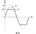
Shown in equation 1, output signal Vo increases along with the increase of audio signal Vin.If owing to the further increase of audio signal Vin causes the peak value summit Vp beyond supply voltage VCC of output signal Vo, shown in Fig. 3 A or Fig. 3 B, output signal Vo is at the output level clipped wave corresponding to supply voltage VCC so.If traditional D class A amplifier A circuit is analog amplifier circuit but not digital amplifier circuit, so as shown in Figure 3A, output signal Vo is by slicing simply.Here, output signal Vo has the distortion component that is defined as D1.Yet if traditional D class A amplifier A circuit is mainly as the PWM switching amplifier of digital amplifier circuit, output signal Vo has waveform shown in Fig. 3 B when clipped wave so.In such output signal Vo,,, there is other stairstepping high frequency distortion component D2 on distortion component D1 next door at the edge of its slicing part.
Can understand the generation of the other stairstepping high frequency distortion component D2 shown in Fig. 3 B with reference to the built-in function waveform of digital amplifier circuit shown in Figure 4.As shown in Figure 4, the signal Vea of amplifier 110 increases gradually and compares the clipped wave up to output signal Vo with triangular signal.Thereby the duty ratio of pwm signal increases gradually and approximate reaches 100%.Should be noted that it is the moment that the output signal Vo of amplifier 110 increases to supply voltage VCC that duty ratio reaches moment of 100%.Thereby, although audio signal Vin is further amplified after this moment, output signal Vo clipped wave, it is no more than supply voltage VCC.Here, the signal Vea from amplifier 110 outputs surpasses the scope of triangular signal and enters saturation condition.If audio signal Vin is weakened by peak value summit Vp and the value of audio signal Vin becomes less than the value of feedback of the output signal Vo of slicing, so from the signal Vea of amplifier 110 outputs by saturation condition and the scope that enters triangular signal.Because the characteristic of integrator, so inevitable time of origin postpones.Signal Vea is delayed with by saturation condition and the scope that enters triangular signal.Because the characteristic of integrator causes output signal Vo to be continued slicing in time of delay, the scope that enters triangular signal from the signal Vea of amplifier 110 outputs enters normal PWM operation then.After this, output signal Vo with precipitous graded to follow output fast corresponding to audio signal Vin.Thereby, the stairstepping distortion takes place.
From the signal Vea of amplifier 110 output must be in the triangular wave scope to improve the stairstepping high frequency distortion component D2 that is produced when the output signal Vea clipped wave.In order to realize this purpose, use input chopper that audio signal Vin is limited in suitable level or littler.Described input chopper can have the structure shown in Fig. 2 A or Fig. 2 B usually.This structure construction is simple, but the level that will limit is restricted to Zener voltage or diode voltage.Thereby, be difficult to freely change level.As a result, be difficult to accurately tackle the variation of amplifier gain or supply voltage.In addition, the upper and lower clipped wave of excessive input during conditioning.Thereby, output distortion.
Summary of the invention
Exemplary embodiment of the present invention overcomes above shortcoming and above other shortcoming of not describing.In addition, the present invention does not need to overcome above-mentioned shortcoming, and exemplary embodiment of the present invention can not overcome above-mentioned any problem.
The invention provides a kind of like this input-gain control apparatus and method of audio frequency amplifier, in the audio frequency apparatus that comprises acoustic amplifier and switching amplifier, if acoustical signal is not imported in dynamic range, the gain of cutting down acoustical signal based on the cut-off level that sets in advance automatically of this equipment and method is with the distortion minimization of the acoustical signal that will cause owing to the slicing of acoustical signal so, thereby the excessive input of limit acoustic signal is with the acoustical signal in the input dynamic range.
According to an aspect of the present invention, a kind of input-gain control apparatus of audio frequency amplifier is provided, this input-gain control apparatus comprises: voltage detector, detect the voltage difference voltage between beyond supply voltage and the allowance voltage whether of the output signal of audio frequency amplifier; And input chopper, according to the gain of the testing result of voltage detector restriction input signal, so that the voltage of output signal is no more than described difference voltage.
Voltage detector can comprise: the constant voltage unit, determine to supply voltage to be the allowance voltage of constant; Voltage divider is determined the gentle level down of powering on of described difference voltage; With first switch element, surpass the described gentle voltage of level down that powers on if exist, carry out switching manipulation so.
The constant voltage unit can be a Zener diode.Voltage divider can comprise: first resistance R 1 and second resistance R 2 are used for determining the described level of going up; With the 3rd resistance R 3 and the 4th resistance R 4, be used for determining described level down.
First switch element can be a switch element.That described switch element can comprise is negative-just-and negative (NPN) transistor npn npn or Negative-Positive-Negative (PNP) transistor npn npn.
Input chopper can comprise: the second switch unit, carry out switching manipulation according to switching signal; And output impedance, the gain of cutting down input signal according to switching manipulation.Output impedance can be resistance.
Can use equation
Calculate the described voltage V that goes up level
UL, wherein, V
DZ1Indicate the reverse voltage of the first Zener diode DZ1.
Can use equation
Calculate the described voltage V of level down
LL, wherein, V
DZ2Indicate the reverse voltage of the second Zener diode DZ2.
The resistance ratio of voltage divider can be " R1: R2=R3: R4 ".
According to a further aspect in the invention, provide a kind of input gain control method of audio frequency amplifier, this method comprises: the voltage difference voltage between beyond supply voltage and the allowance voltage whether that detects the output signal of audio frequency amplifier; With gain, so that the voltage of output signal is no more than described difference voltage according to testing result restriction input signal.
Detect audio frequency amplifier output signal voltage whether the step of the difference voltage between beyond supply voltage and the allowance voltage can comprise: definite is the allowance voltage of constant to supply voltage; Determine the gentle level down of powering on of described difference voltage; Surpass the described gentle voltage of level down that powers on if exist, carry out switching manipulation so.
Can use constant voltage elements to determine allowance voltage.
Can use first and second resistance to determine the described level of going up, can use third and fourth resistance to determine described level down.
Resistance ratio between first and second resistance can equal the resistance ratio between third and fourth resistance.
Can use equation
Calculate the described voltage V that goes up level
UL, wherein, V
DZ1Indicate the reverse voltage of the first Zener diode DZ1.
Can use equation
Calculate the described voltage V of level down
LL, wherein, V
DZ2Indicate the reverse voltage of the second Zener diode DZ2.
According to the step of the gain of testing result restriction input signal so that the voltage of output signal is no more than the step of described difference voltage can comprise: carry out switching manipulation according to switching signal; With the gain of cutting down input signal according to switching manipulation.
Description of drawings
By below in conjunction with the description that accompanying drawing carried out, the above-mentioned and/or others of certain exemplary embodiments of the present invention will become apparent, wherein:
Fig. 1 is the schematic diagram of structure that the D class A amplifier A circuit of prior art is shown;
Fig. 2 A and Fig. 2 B are the circuit diagrams that the amplitude limiter circuit of prior art is shown;
Fig. 3 A and Fig. 3 B are the curve charts that the slicing of the output voltage that takes place when the Vp beyond supply voltage VCC of the peak value summit of output voltage is shown;
Fig. 4 is the curve chart that the built-in function waveform of audio-frequency amplifier circuit is shown;
Fig. 5 illustrates the circuit diagram of the input-gain control apparatus of audio frequency amplifier according to an exemplary embodiment of the present invention; With
Fig. 6 is the curve chart that the waveform of the output voltage of exporting in allowance voltage according to an exemplary embodiment of the present invention is shown.
Embodiment
Come to describe in further detail certain exemplary embodiments of the present invention with reference to the accompanying drawings.Run through accompanying drawing, identical label will be understood that to represent components identical, feature and structure.
The content such as detailed structure and element that defines in the description just is provided to help complete understanding content of the present invention.Therefore, it will be understood by those skilled in the art that under the situation that does not break away from the spirit and scope of the present invention, can carry out various changes and modification exemplary embodiment described herein.In addition, for clarity and conciseness, from describe, known function or structure have been omitted.
An aspect of of the present present invention be to weaken excessive input signal to prevent because the clipping distortion D1 that excessive input causes, excessive output and because the saturated step-like high frequency distortion D2 that causes of the internal block of audio frequency amplifier, no matter thereby the variation of the gain and the supply voltage VCC of audio frequency amplifier is how, output signal all keep off audio frequency amplifier supply voltage VCC but in allowance voltage dV.In addition, can cut down whole gain rather than cut away excessive input component simply with the restriction incoming level, keeping the primitive form of input signal, thereby with the distortion minimization of input signal.In addition, can adjust the level that allowance voltage dV changes export-restriction, depend on the amplifier of the power output with change of product with design with reference to supply voltage VCC.Thereby, can be to have the loudspeaker impedance identical and supply voltage with Amplifier Design to share loud speaker and power module with the amplifier of previous design.
Fig. 5 illustrates the circuit diagram of the input-gain control apparatus of audio frequency amplifier according to an exemplary embodiment of the present invention.With reference to Fig. 5, the input-gain control apparatus of audio frequency amplifier comprises input unit 510, voltage detector 520 and input chopper 530 according to an exemplary embodiment of the present invention.
Described input-gain control apparatus also comprises comparator 120, gate drivers 130, low pass filter (LPF) 140 and triangular-wave generator 150 as shown in Figure 1.Below describe the structure of comparator 120, gate drivers 130, LPF 140 and triangular-wave generator 150, thereby will omit their detailed description here.
In input unit 510, capacitor C 1 and input resistance Rin are connected between input port INPUT and the input power supply Vin.
Here, voltage detector 520 comprises constant voltage unit 522, voltage divider 524 and first switch element 526.Constant voltage unit 522 determines to supply voltage VCC to be the allowance voltage dV of constant.Voltage divider 524 is determined the gentle level down of powering on of different voltages.First switch element 526 is carried out switching manipulation according to surpassing the gentle voltage of level down that powers on.
Here, constant voltage unit 522 comprises the first Zener diode DZ1 and the second Zener diode DZ2, and voltage divider 524 comprises first resistance R 1, second resistance R 2, the 3rd resistance R 3 and the 4th resistance R 4.In addition, first switch element 526 comprise negative-just-negative (NPN) type (second) transistor Q2 and Negative-Positive-Negative (PNP) type (the 4th) transistor Q4.
In other words, as shown in Figure 5, in voltage detector 520, the first Zener diode DZ1, first resistance R 1, second resistance R 2, the 4th resistance R 4, the 3rd resistance R 3 and the second Zener diode DZ2 are connected between positive voltage+VCC and the negative supply voltage-VCC.Here, the base stage of transistor seconds Q2 is connected to the tie point between first resistance R 1 and second resistance R 2, and the collector electrode of transistor seconds Q2 is connected to the tie point between the positive voltage+VCC and the first Zener diode DZ1.The emitting stage of transistor seconds Q2 is connected to negative supply voltage-VCC and input chopper 530 by resistance R.
In addition, the base stage of the 4th transistor Q4 is connected to the tie point between the 3rd resistance R 3 and the 4th resistance R 4, and the transmitter of the 4th transistor Q4 is connected to positive voltage+VCC by resistance R.In addition, the collector electrode of the 4th transistor Q4 is connected to the tie point between the negative supply voltage-VCC and the second Zener diode DZ2.
Here, second switch unit 532 comprises positive-negative-positive (first) transistor Q1 and NPN type (the 3rd) transistor Q3, and output impedance 534 comprises output resistance Ro.
In other words, in input chopper 530, the base stage of the first transistor Q1 is connected to the emitter of the transistor seconds Q2 of voltage detector 520, and the collector electrode of the first transistor Q1 is connected to negative supply voltage-VCC, and the emitter of the first transistor Q1 is connected to output resistance Ro.In addition, the base stage of the 3rd transistor Q3 is connected to the emitter of the 4th transistor Q4, and the collector electrode of the 3rd transistor Q3 is connected to positive voltage+VCC, and the emitter of the 3rd transistor Q3 is connected to output resistance Ro.Output resistance Ro is connected to the tie point between input port INPUT and the input resistance Rin.
Here, output resistance Ro can be a variable resistor element, and it can change resistance value to adjust the reduction of gain.
Resistance ratio between first resistance R 1 and second resistance R 2 equals the resistance ratio between the 3rd resistance R 3 and the 4th resistance R 4, and allowance voltage dV is meant the voltage that the do not allow output signal voltage near supply voltage VCC.
Description is according to the operation of the input-gain control apparatus of the audio frequency amplifier of this exemplary embodiment now.
In order to describe the operation of input-gain control apparatus, suppose that input-gain control apparatus shown in Figure 5 is constructed to the importation of audio frequency amplifier shown in Figure 1.
Here, when the voltage beyond supply voltage VCC of output signal and the difference voltage between the allowance voltage dV, the input-gain control apparatus operation.If surpassing from supply voltage VCC, the voltage of output signal deducts the difference voltage that allowance voltage dV (that is, the Zener voltage of the first Zener diode DZ1) obtains, so because first resistance R 1 and second resistance R 2 cause voltage to reduce.Here, the electric current of first resistance R, 1 generation is provided for the base stage of transistor seconds Q2 with operation transistor seconds Q2.
If surpassing from supply voltage-VCC, the voltage of output signal deducts the difference voltage that allowance voltage dV (that is, the Zener voltage of the second Zener diode DZ2) obtains, so because the 3rd resistance R 3 causes voltage to reduce.Here, according to the electric current that the 3rd resistance R 3 produces, the base stage of the 4th transistor Q4 becomes low level to operate the 4th transistor Q4.
The first transistor Q1 of input chopper 530 and the 3rd transistor Q3 are along with the operation of the transistor seconds Q2 of voltage detector 520 and the 4th transistor Q4 and operate.
Here, if the conducting voltage of the base stage of the first transistor Q1, transistor seconds Q2, the 3rd transistor Q3 and the 4th transistor Q4 equals the conducting voltage of the emitter of the first transistor Q1, transistor seconds Q2, the 3rd transistor Q3 and the 4th transistor Q4, the last level that obtains import-restriction shown in Equation 2 so (is gone up level voltage V
UL), obtain following level (the following level voltage V of import-restriction shown in Equation 3
LL):
Wherein, V
DZ1Indicate the reverse voltage of the first Zener diode DZ1.
Wherein, V
DZ2Indicate the reverse voltage of the second Zener diode DZ2.
The voltage of the first Zener diode DZ1 and the second Zener diode DZ2 is set to have identical value.
The electric current that operation by the first transistor Q1 and the 3rd transistor Q3 produces is provided for output resistance Ro, and output resistance Ro is adjusted into the level of input signal in allowance voltage dV.
If, can obtain the voltage Vclip of output signal shown in Equation 4 so in clipping level owing to feedback resistance shown in Equation 1 obtains to gain and the resistance ratio of voltage divider is " R1: R2=R3: R4=Ra: Rb ":
Because equation 4 has provided the clipping level of output signal, thus though the variation of supply voltage VCC how, allowance voltage dV is a constant for supply voltage VCC.In other words, by deducting zener diode voltage V from supply voltage VCC
DZ1Obtain allowance voltage dV, thereby determine allowance voltage dV by the voltage of Zener diode.
In addition, if output impedance Ro is adjusted into suitable value, can remove component so simply above cut-off level.In addition, shown in the figure on the right among Fig. 6, when output impedance Ro is non-vanishing, can on clipping level, add suitable amount.Thereby, can reduce the distortion component D1 that causes by simple slicing considerably.
As mentioned above, in the input-gain control apparatus and method of audio frequency amplifier according to an exemplary embodiment of the present invention, if acoustical signal surpasses dynamic range, can cut down the gain of acoustical signal so based on the cut-off level that sets in advance automatically, so that the acoustical signal in the dynamic range is input in the audio frequency apparatus that comprises acoustic amplifier and switching amplifier.Thereby the distortion minimization of the acoustical signal that the slicing owing to acoustical signal can be caused also can limit excessive input.
As mentioned above, in the input-gain control apparatus and method of audio frequency amplifier according to an exemplary embodiment of the present invention, can only cut down particular level (or bigger) excessive input signal gain rather than simply cut away excessive input signal.Thereby the output waveform distortions that the slicing owing to output waveform can be caused minimizes.Specifically, switching amplifier can prevent the saturated stairstepping high-frequency noise to remove homophonic distortion simultaneously and to take place of internal block during slicing.In addition, the linear analogue amplifier can only be cut down gain rather than simply cut away excessive input signal in the primitive form that keeps excessive input signal, with the distortion minimization with output signal.
Electrical equipment with audio-frequency function can use same supply voltage at random to adjust to be operating as the gain that is used to limit output level to cut down the reference voltage of the output comparator circuit of circuit.Thereby, need not change power supply or loudspeaker impedance, just can obtain the shown effect that goes out when power supply or loudspeaker impedance change.Therefore, can the supply voltage and the loudspeaker impedance standardization of the product of various output specifications will be had.
Described embodiments of the invention are exemplary, it should be construed as limiting the invention.Exemplary teachings of the present invention easily can be applied to the equipment of other type.In addition, the description of exemplary embodiment of the present is exemplary, it or not the scope of restriction claim, under the situation of the spirit and scope of the present invention that four corner limited that do not break away from claim and equivalent thereof, many replacements, modifications and variations will be clearly for those skilled in the art.
Claims (16)
1, a kind of input-gain control apparatus of audio frequency amplifier, this input-gain control apparatus comprises:
Voltage detector, whether the voltage of the output signal of detection audio frequency amplifier surpasses the difference voltage as the voltage difference between supply voltage and the allowance voltage; With
Input chopper according to the gain of the testing result of voltage detector restriction input signal, surpasses described difference voltage with the voltage that prevents output signal.
2, input-gain control apparatus as claimed in claim 1, wherein, voltage detector comprises:
The constant voltage unit determines to supply voltage to be the allowance voltage of constant;
Voltage divider is determined the gentle level down of powering on of described difference voltage; With
First switch element if the voltage of output signal surpasses the last level of described difference voltage and is reduced to the following level that is lower than described difference voltage, is carried out switching manipulation so.
3, input-gain control apparatus as claimed in claim 2, wherein, the constant voltage unit comprises Zener diode.
4, input-gain control apparatus as claimed in claim 2, wherein, voltage divider comprises:
First resistance R 1 and second resistance R 2 are determined the last level of described difference voltage; With
The 3rd resistance R 3 and the 4th resistance R 4 are determined the following level of described difference voltage.
5, input-gain control apparatus as claimed in claim 2, wherein, first switch element is a switch element.
6, input-gain control apparatus as claimed in claim 5, wherein, described switch element comprises one of NPN transistor and PNP transistor.
7, input-gain control apparatus as claimed in claim 1, wherein, input chopper comprises:
Switching manipulation is carried out according to switching signal in the second switch unit; With
Output impedance, the gain of cutting down input signal according to switching manipulation.
8, input-gain control apparatus as claimed in claim 7, wherein, output impedance is resistance.
9, input-gain control apparatus as claimed in claim 7, wherein, output impedance is variable resistor.
10, input-gain control apparatus as claimed in claim 4, wherein, the resistance ratio of voltage divider is R1: R2=R3: R4.
11, a kind of input gain control method of audio frequency amplifier, this method comprises:
Whether the voltage of the output signal of detection audio frequency amplifier surpasses the difference voltage as the voltage difference between supply voltage and the allowance voltage; With
According to the gain of testing result restriction input signal, surpass described difference voltage with the voltage that prevents output signal.
12, input gain control method as claimed in claim 11, wherein, the step whether voltage of the output signal of detection audio frequency amplifier surpasses described difference voltage comprises:
Determine to supply voltage to be the allowance voltage of constant;
Determine the gentle level down of powering on of described difference voltage; With
If the voltage of output signal surpasses the last level of described difference voltage and is reduced to the following level that is lower than described difference voltage, carry out switching manipulation so.
13, input gain control method as claimed in claim 12 wherein, uses constant voltage elements to determine allowance voltage.
14, input gain control method as claimed in claim 12 wherein, uses first and second resistance to determine the last level of described difference voltage, uses third and fourth resistance to determine the following level of described difference voltage.
15, input gain control method as claimed in claim 14, wherein, the resistance ratio between first and second resistance equals the resistance ratio between third and fourth resistance.
16, input gain control method as claimed in claim 11, wherein, the step that limits the gain of input signal according to testing result comprises:
Carry out switching manipulation according to switching signal; With
Cut down the gain of input signal according to switching manipulation.
Applications Claiming Priority (2)
| Application Number | Priority Date | Filing Date | Title |
|---|---|---|---|
| KR1020060051032 | 2006-06-07 | ||
| KR1020060051032A KR20070117171A (en) | 2006-06-07 | 2006-06-07 | Input-gain control apparatus and method |
Publications (1)
| Publication Number | Publication Date |
|---|---|
| CN101087126A true CN101087126A (en) | 2007-12-12 |
Family
ID=38511382
Family Applications (1)
| Application Number | Title | Priority Date | Filing Date |
|---|---|---|---|
| CNA2007100982081A Pending CN101087126A (en) | 2006-06-07 | 2007-04-13 | Input-gain control apparatus and method |
Country Status (4)
| Country | Link |
|---|---|
| US (1) | US20070285160A1 (en) |
| EP (1) | EP1865598A3 (en) |
| KR (1) | KR20070117171A (en) |
| CN (1) | CN101087126A (en) |
Cited By (1)
| Publication number | Priority date | Publication date | Assignee | Title |
|---|---|---|---|---|
| CN103326677A (en) * | 2012-03-22 | 2013-09-25 | 炬力集成电路设计有限公司 | Audio power amplifier and adjusting method thereof |
Families Citing this family (13)
| Publication number | Priority date | Publication date | Assignee | Title |
|---|---|---|---|---|
| JP5664265B2 (en) * | 2011-01-19 | 2015-02-04 | ヤマハ株式会社 | Dynamic range compression circuit |
| US9124461B2 (en) * | 2011-07-18 | 2015-09-01 | Marvell Israel (M.I.S.L) Ltd. | Method and apparatus for reducing jitter |
| KR101723181B1 (en) * | 2015-02-23 | 2017-04-05 | 주식회사 인터엠 | Audio amplifier apparatus |
| US9607603B1 (en) * | 2015-09-30 | 2017-03-28 | Cirrus Logic, Inc. | Adaptive block matrix using pre-whitening for adaptive beam forming |
| GB2547799A (en) * | 2016-02-26 | 2017-08-30 | Cirrus Logic Int Semiconductor Ltd | Clamping audio signal paths |
| GB2547730B (en) * | 2016-02-26 | 2018-08-01 | Cirrus Logic Int Semiconductor Ltd | Clamping audio signal paths |
| US11107453B2 (en) | 2019-05-09 | 2021-08-31 | Dialog Semiconductor B.V. | Anti-noise signal generator |
| US10861433B1 (en) | 2019-05-09 | 2020-12-08 | Dialog Semiconductor B.V. | Quantizer |
| US10784890B1 (en) * | 2019-05-09 | 2020-09-22 | Dialog Semiconductor B.V. | Signal processor |
| US11329634B1 (en) | 2019-05-09 | 2022-05-10 | Dialog Semiconductor B.V. | Digital filter structure |
| US10848174B1 (en) | 2019-05-09 | 2020-11-24 | Dialog Semiconductor B.V. | Digital filter |
| US10972123B1 (en) | 2019-05-09 | 2021-04-06 | Dialog Semiconductor B.V. | Signal processing structure |
| US11706062B1 (en) | 2021-11-24 | 2023-07-18 | Dialog Semiconductor B.V. | Digital filter |
Family Cites Families (15)
| Publication number | Priority date | Publication date | Assignee | Title |
|---|---|---|---|---|
| US4301445A (en) * | 1979-12-10 | 1981-11-17 | General Electric Company | Communication system and method having wide dynamic range digital gain control |
| US4459557A (en) * | 1982-02-04 | 1984-07-10 | Mcquilken Mark A | Compressor limiter for audio signal processing |
| US4457203A (en) * | 1982-03-09 | 1984-07-03 | Wright-Malta Corporation | Sound signal automatic detection and display method and system |
| US4881047A (en) * | 1988-06-20 | 1989-11-14 | Waller Jr James K | Automatic gain expansion system |
| US5151939A (en) * | 1990-03-21 | 1992-09-29 | Delco Electronics Corporation | Adaptive audio processor for am stereo signals |
| US5260674A (en) * | 1992-08-04 | 1993-11-09 | Acrodyne Industries, Inc. | Amplitude modulator |
| US5329243A (en) * | 1992-09-17 | 1994-07-12 | Motorola, Inc. | Noise adaptive automatic gain control circuit |
| JP2889803B2 (en) * | 1993-11-22 | 1999-05-10 | 三洋電機株式会社 | Level setting circuit |
| JP3526719B2 (en) * | 1997-03-19 | 2004-05-17 | 富士通株式会社 | Automatic threshold control circuit and signal amplifier circuit |
| US6107875A (en) * | 1998-10-15 | 2000-08-22 | Intersil Corporation | Variable frequency class D modulator with built in soft clipping and frequency limiting |
| US6765436B1 (en) * | 2002-09-04 | 2004-07-20 | Cirrus Logic, Inc. | Power supply based audio compression for digital audio amplifier |
| US8005230B2 (en) * | 2002-12-20 | 2011-08-23 | The AVC Group, LLC | Method and system for digitally controlling a multi-channel audio amplifier |
| JP3922182B2 (en) * | 2002-12-27 | 2007-05-30 | ヤマハ株式会社 | Amplifier circuit |
| TWI344752B (en) * | 2004-10-18 | 2011-07-01 | Monolithic Power Systems Inc | Method for high efficiency audio amplifier |
| JP5270071B2 (en) * | 2006-05-16 | 2013-08-21 | 富士通オプティカルコンポーネンツ株式会社 | Signal amplification device |
-
2006
- 2006-06-07 KR KR1020060051032A patent/KR20070117171A/en not_active Application Discontinuation
-
2007
- 2007-03-19 US US11/723,249 patent/US20070285160A1/en not_active Abandoned
- 2007-03-20 EP EP07104520A patent/EP1865598A3/en not_active Withdrawn
- 2007-04-13 CN CNA2007100982081A patent/CN101087126A/en active Pending
Cited By (2)
| Publication number | Priority date | Publication date | Assignee | Title |
|---|---|---|---|---|
| CN103326677A (en) * | 2012-03-22 | 2013-09-25 | 炬力集成电路设计有限公司 | Audio power amplifier and adjusting method thereof |
| CN103326677B (en) * | 2012-03-22 | 2016-05-04 | 炬芯(珠海)科技有限公司 | The control method of audio-frequency power amplifier and audio-frequency power amplifier |
Also Published As
| Publication number | Publication date |
|---|---|
| EP1865598A2 (en) | 2007-12-12 |
| KR20070117171A (en) | 2007-12-12 |
| EP1865598A3 (en) | 2008-08-27 |
| US20070285160A1 (en) | 2007-12-13 |
Similar Documents
| Publication | Publication Date | Title |
|---|---|---|
| CN101087126A (en) | Input-gain control apparatus and method | |
| EP1860772A2 (en) | Automatic input-gain control circuit and method thereof | |
| US7425864B2 (en) | Recovery from clipping events in a class D amplifier | |
| CN1770623B (en) | Method for high efficiency audio amplifier | |
| US9525385B2 (en) | Device and method for reducing clipping in an amplifier | |
| CN101557203A (en) | Power amplifier with overcurrent protection | |
| US8525593B2 (en) | Circuit and method for amplifying a digital signal | |
| CN101110569A (en) | Abnormality detection circuit | |
| CN211405976U (en) | Audio amplifier and integrated circuit | |
| EP0054943B2 (en) | Power amplifier for supplying electric power to a load by switching of power supply voltage | |
| US20040222845A1 (en) | Class-D power amplifier capable of eliminating excessive response phenomenon when returning to a steady state from an abnormal state and an amplification method thereof | |
| US6489840B2 (en) | Power amplification equipment | |
| CN112803905B (en) | Compensation circuit | |
| USRE33333E (en) | Digital audio amplifier having a high power output level and low distortion | |
| JP3068642B2 (en) | Circuit for detecting output distortion | |
| CN203775149U (en) | Class-D power amplification chip with power limiting function and audio play device | |
| Bellili et al. | Low power class D audio amplifier with high performance and high efficiency | |
| CN101197557A (en) | Audio power amplifier | |
| KR100226227B1 (en) | Self-oscillation type delta modulation d-type audio amplifier | |
| CN100477506C (en) | Circuit for class D amplifier | |
| JPH03175709A (en) | Power control circuit for high frequency amplifier | |
| JP3811030B2 (en) | Digital amplifier | |
| CN214799419U (en) | Single-power-supply operational amplifier circuit | |
| CN218998026U (en) | Sound box output power compression control circuit and power amplifier | |
| EP4117179A1 (en) | Audio processor |
Legal Events
| Date | Code | Title | Description |
|---|---|---|---|
| C06 | Publication | ||
| PB01 | Publication | ||
| C02 | Deemed withdrawal of patent application after publication (patent law 2001) | ||
| WD01 | Invention patent application deemed withdrawn after publication |