CN100590651C - Pixel interpolation circuit and pixel interpolation method - Google Patents
Pixel interpolation circuit and pixel interpolation method Download PDFInfo
- Publication number
- CN100590651C CN100590651C CN200480033136.7A CN200480033136A CN100590651C CN 100590651 C CN100590651 C CN 100590651C CN 200480033136 A CN200480033136 A CN 200480033136A CN 100590651 C CN100590651 C CN 100590651C
- Authority
- CN
- China
- Prior art keywords
- pixel
- interpolation
- circuit
- missing
- data
- Prior art date
- Legal status (The legal status is an assumption and is not a legal conclusion. Google has not performed a legal analysis and makes no representation as to the accuracy of the status listed.)
- Expired - Fee Related
Links
- 238000000034 method Methods 0.000 title claims description 48
- 238000001514 detection method Methods 0.000 claims description 6
- 230000008034 disappearance Effects 0.000 claims 32
- 239000000654 additive Substances 0.000 claims 8
- 230000000996 additive effect Effects 0.000 claims 8
- 238000007689 inspection Methods 0.000 claims 1
- 230000002950 deficient Effects 0.000 abstract 1
- 238000012360 testing method Methods 0.000 description 246
- 238000004364 calculation method Methods 0.000 description 171
- 238000012423 maintenance Methods 0.000 description 141
- 238000010586 diagram Methods 0.000 description 90
- 238000011156 evaluation Methods 0.000 description 54
- 238000012545 processing Methods 0.000 description 11
- 238000012854 evaluation process Methods 0.000 description 9
- 238000012935 Averaging Methods 0.000 description 7
- 230000000737 periodic effect Effects 0.000 description 7
- 240000001973 Ficus microcarpa Species 0.000 description 3
- 238000012217 deletion Methods 0.000 description 3
- 230000037430 deletion Effects 0.000 description 3
- 230000006870 function Effects 0.000 description 3
- 230000007274 generation of a signal involved in cell-cell signaling Effects 0.000 description 3
- 238000003384 imaging method Methods 0.000 description 2
- 239000011295 pitch Substances 0.000 description 2
- 238000005070 sampling Methods 0.000 description 2
- 230000000007 visual effect Effects 0.000 description 2
- 238000012937 correction Methods 0.000 description 1
- 230000000694 effects Effects 0.000 description 1
- 239000011159 matrix material Substances 0.000 description 1
Images


Classifications
-
- G—PHYSICS
- G06—COMPUTING; CALCULATING OR COUNTING
- G06T—IMAGE DATA PROCESSING OR GENERATION, IN GENERAL
- G06T3/00—Geometric image transformations in the plane of the image
- G06T3/40—Scaling of whole images or parts thereof, e.g. expanding or contracting
- G06T3/4007—Scaling of whole images or parts thereof, e.g. expanding or contracting based on interpolation, e.g. bilinear interpolation
-
- G—PHYSICS
- G06—COMPUTING; CALCULATING OR COUNTING
- G06T—IMAGE DATA PROCESSING OR GENERATION, IN GENERAL
- G06T5/00—Image enhancement or restoration
- G06T5/20—Image enhancement or restoration using local operators
-
- G—PHYSICS
- G06—COMPUTING; CALCULATING OR COUNTING
- G06T—IMAGE DATA PROCESSING OR GENERATION, IN GENERAL
- G06T5/00—Image enhancement or restoration
- G06T5/77—Retouching; Inpainting; Scratch removal
-
- H—ELECTRICITY
- H04—ELECTRIC COMMUNICATION TECHNIQUE
- H04N—PICTORIAL COMMUNICATION, e.g. TELEVISION
- H04N1/00—Scanning, transmission or reproduction of documents or the like, e.g. facsimile transmission; Details thereof
- H04N1/40—Picture signal circuits
- H04N1/401—Compensating positionally unequal response of the pick-up or reproducing head
Landscapes
- Engineering & Computer Science (AREA)
- Physics & Mathematics (AREA)
- General Physics & Mathematics (AREA)
- Theoretical Computer Science (AREA)
- Multimedia (AREA)
- Signal Processing (AREA)
- Television Systems (AREA)
- Transforming Light Signals Into Electric Signals (AREA)
- Image Processing (AREA)
- Facsimile Image Signal Circuits (AREA)
- Color Television Image Signal Generators (AREA)
- Image Input (AREA)
- Picture Signal Circuits (AREA)
Abstract
Description
技术领域 technical field
本发明涉及对数字图像中的缺失像素进行插值的插值运算电路、像素插值电路、插值运算方法以及像素插值方法。The invention relates to an interpolation operation circuit for interpolating missing pixels in a digital image, a pixel interpolation circuit, an interpolation operation method and a pixel interpolation method.
背景技术 Background technique
在现有的像素插值电路中,使用以下方法计算缺失像素的插值数据:以与缺失像素邻接的像素的值的平均值作为插值数据的方法;用最小二乘法求出与缺失像素邻接的像素的回归直线,根据该回归直线计算插值数据的方法;以及根据与缺失像素邻接的4个像素求出4次式的曲线,根据该4次式计算插值数据的方法等(例如,参照专利文献1)。In the existing pixel interpolation circuit, the following methods are used to calculate the interpolation data of the missing pixel: the method of using the average value of the values of the pixels adjacent to the missing pixel as the interpolation data; A regression line, a method of calculating interpolation data from the regression line; and a method of calculating a quartic curve from four pixels adjacent to the missing pixel, and calculating interpolation data from the quartic (for example, refer to Patent Document 1) .
专利文献1:日本特开2003-101724公报(段落0040至0066,图3至图5)Patent Document 1: Japanese Patent Application Laid-Open No. 2003-101724 (paragraphs 0040 to 0066, FIGS. 3 to 5 )
发明内容 Contents of the invention
在现有的插值运算电路中进行线性插值或使用高次函数进行插值,所以对缺失了一部分像素的周期性高的图像进行插值时,误差增大。Since linear interpolation or interpolation using a higher-order function is performed in a conventional interpolation operation circuit, an error increases when an image with high periodicity in which some pixels are missing is interpolated.
本发明就是为了解决如上所述的问题而完成,其目的在于得到可以适当地对周期性高的图像中所包含的缺失像素进行插值的插值运算电路、像素插值电路、插值运算方法以及图像插值方法。The present invention was made to solve the above problems, and its object is to obtain an interpolation operation circuit, a pixel interpolation circuit, an interpolation operation method, and an image interpolation method that can appropriately interpolate missing pixels included in an image with high periodicity .
本发明提供平均维持插值运算电路,其特征在于,求出缺失像素的插值数据,使得构成包含缺失像素的像素组的多个像素的值的平均值和构成不包含缺失像素的像素组的多个像素的值的平均值相等。The present invention provides an average maintaining interpolation operation circuit, characterized in that the interpolation data of missing pixels is obtained such that the average value of the values of a plurality of pixels constituting a pixel group including missing pixels is equal to the average value of the values of a plurality of pixels constituting a group of pixels not including missing pixels. The average value of the pixel's value is equal.
在基于本发明的插值运算电路中,求出缺失像素的插值数据,使得包含缺失像素的像素列的平均值和不包含缺失像素的像素列的平均值相等,所以可以适当地对包含缺失像素的像素列和不包含缺失像素的像素列的像素的值的平均值相等的数据、例如具有周期性的数据等进行插值。In the interpolation operation circuit based on the present invention, the interpolation data of the missing pixel is obtained, so that the average value of the pixel column containing the missing pixel is equal to the average value of the pixel column not containing the missing pixel, so the data of the missing pixel can be appropriately calculated. Interpolation is performed on data in which the average values of the pixel values of the pixel row and the pixel row not including missing pixels are equal, for example, periodic data.
附图说明 Description of drawings
图1是表示实施方式1的插值运算电路的结构的方框图。FIG. 1 is a block diagram showing the configuration of an interpolation calculation circuit according to the first embodiment.
图2是表示由实施方式1的插值运算电路处理的像素列的图。FIG. 2 is a diagram showing a pixel row processed by an interpolation operation circuit according to
图3是表示由实施方式1的插值运算电路处理的像素数据的一例的波形图。FIG. 3 is a waveform diagram showing an example of pixel data processed by the interpolation arithmetic circuit according to
图4是表示由实施方式1的插值运算电路处理的像素数据的一例的波形图。4 is a waveform diagram showing an example of pixel data processed by the interpolation arithmetic circuit of the first embodiment.
图5是表示由实施方式1的插值运算电路处理的像素数据的一例的波形图。5 is a waveform diagram showing an example of pixel data processed by the interpolation arithmetic circuit according to the first embodiment.
图6是表示具有周期检测电路的像素插值电路的结构例的方框图。FIG. 6 is a block diagram showing a configuration example of a pixel interpolation circuit having a cycle detection circuit.
图7是表示由实施方式2的插值运算电路处理的像素列的图。FIG. 7 is a diagram showing pixel columns processed by an interpolation calculation circuit according to
图8是表示由实施方式2的插值运算电路处理的像素数据的一例的波形图。8 is a waveform diagram showing an example of pixel data processed by the interpolation arithmetic circuit according to the second embodiment.
图9是表示由实施方式2的插值运算电路处理的像素数据的一例的波形图。9 is a waveform diagram showing an example of pixel data processed by the interpolation arithmetic circuit according to the second embodiment.
图10是表示实施方式3的插值运算电路的结构的方框图。FIG. 10 is a block diagram showing the configuration of an interpolation calculation circuit according to
图11是表示由实施方式3的插值运算电路处理的像素列的图。FIG. 11 is a diagram showing pixel columns processed by an interpolation calculation circuit according to
图12是表示由实施方式3的插值运算电路处理的、被分割为多个行的像素的组的图。FIG. 12 is a diagram showing groups of pixels divided into a plurality of rows processed by the interpolation calculation circuit according to
图13是表示由本发明的插值运算电路处理的、位于多个行的像素列的图。Fig. 13 is a diagram showing pixel columns located in a plurality of rows processed by the interpolation operation circuit of the present invention.
图14是表示由实施方式3的插值运算电路处理的像素数据的一例的波形图。14 is a waveform diagram showing an example of pixel data processed by the interpolation arithmetic circuit according to the third embodiment.
图15是表示具有多个缺失部加法电路的缺失部合计计算电路的结构例的方框图。15 is a block diagram showing a configuration example of a missing part total calculation circuit having a plurality of missing part adding circuits.
图16是表示平均维持插值运算电路的结构例的方框图。Fig. 16 is a block diagram showing a configuration example of an average maintaining interpolation calculation circuit.
图17是表示实施方式4的像素插值电路的结构的方框图。FIG. 17 is a block diagram showing the configuration of a pixel interpolation circuit according to
图18是表示实施方式4的像素插值电路的、像素周期和插值误差之间的关系的图。18 is a diagram showing a relationship between a pixel cycle and an interpolation error in a pixel interpolation circuit according to
图19(a)至(e)是表示实施方式4的像素插值电路的、对于各个参数k的、像素周期和插值误差之间的关系的图。19( a ) to ( e ) are diagrams showing the relationship between the pixel period and the interpolation error for each parameter k in the pixel interpolation circuit according to the fourth embodiment.
图20(a)至(c)是表示实施方式4的像素插值电路的、对于各个参数k的、像素周期和插值误差之间的关系的图。20( a ) to ( c ) are diagrams showing the relationship between the pixel period and the interpolation error for each parameter k in the pixel interpolation circuit according to the fourth embodiment.
图21是表示实施方式5的像素插值电路的结构的方框图。FIG. 21 is a block diagram showing the configuration of a pixel interpolation circuit according to
图22(a)至(d)是表示实施方式5的像素插值电路的左右平均插值电路的动作的波形图。22( a ) to ( d ) are waveform diagrams showing the operation of the left and right average interpolation circuit of the pixel interpolation circuit according to the fifth embodiment.
图23是表示实施方式5的像素插值电路的左右平均插值电路的像素周期和插值误差之间的关系的图。23 is a diagram showing the relationship between the pixel period and the interpolation error of the left-right average interpolation circuit of the pixel interpolation circuit according to the fifth embodiment.
图24(a)至(c)是表示实施方式5的像素插值电路的各插值运算电路的像素周期和插值误差之间的关系的图。24( a ) to ( c ) are diagrams showing the relationship between the pixel period and the interpolation error of each interpolation calculation circuit in the pixel interpolation circuit according to the fifth embodiment.
图25是表示实施方式5的像素插值运算电路的、参数k和插值误差之间的关系的图。25 is a diagram showing a relationship between a parameter k and an interpolation error in the pixel interpolation operation circuit according to
图26(a)至(c)是表示实施方式5的像素插值运算电路的、参数k和插值误差之间的关系的图。26( a ) to ( c ) are diagrams showing the relationship between the parameter k and the interpolation error in the pixel interpolation calculation circuit according to the fifth embodiment.
图27(a)至(c)是表示由实施方式5的像素插值电路处理的像素列的图。27( a ) to ( c ) are diagrams showing pixel columns processed by the pixel interpolation circuit according to the fifth embodiment.
图28(a)至(c)是表示在实施方式5中、像素插值电路的多个平均维持插值运算电路分别带来良好的结果的范围的图。28( a ) to ( c ) are diagrams showing the ranges in which a plurality of average-maintaining interpolation calculation circuits of the pixel interpolation circuit in
图29是表示实施方式6的像素插值电路的结构的方框图。FIG. 29 is a block diagram showing the configuration of a pixel interpolation circuit according to
图30(a)至(b)是表示在实施方式6中处理的像素列以及像素的组的图。30( a ) to ( b ) are diagrams showing pixel columns and pixel groups processed in the sixth embodiment.
图31是表示由实施方式6的像素插值电路对于多个测试像素进行插值时的各插值运算电路的评价结果的图。31 is a diagram showing evaluation results of each interpolation operation circuit when interpolation is performed on a plurality of test pixels by the pixel interpolation circuit according to
图32是表示实施方式6的像素插值电路的各插值运算电路的综合评价结果的图。FIG. 32 is a diagram showing overall evaluation results of each interpolation calculation circuit of the pixel interpolation circuit according to
图33是表示实施方式6的像素插值电路的具体例的方框图。FIG. 33 is a block diagram showing a specific example of a pixel interpolation circuit according to
图34(a)是表示由实施方式6的像素插值电路处理的像素数据的一例的波形图,(b)是表示缺失像素以及位于其附近的测试像素的图。34( a ) is a waveform diagram showing an example of pixel data processed by the pixel interpolation circuit of
图35(a)至(c)是表示由实施方式6的像素插值电路处理的像素列的图。35( a ) to ( c ) are diagrams showing pixel columns processed by the pixel interpolation circuit according to the sixth embodiment.
图36(a)至(e)是表示由实施方式6的像素插值电路处理的一系列的像素中的缺失像素以及位于其附近的测试像素的图。36( a ) to ( e ) are diagrams showing missing pixels and test pixels in the vicinity thereof among a series of pixels processed by the pixel interpolation circuit according to
图37(a)至(e)是表示由实施方式6的像素插值电路处理的一系列的像素中的缺失像素以及位于其附近的测试像素的图。37( a ) to ( e ) are diagrams showing missing pixels and test pixels located in the vicinity of a series of pixels processed by the pixel interpolation circuit of
图38(a)至(e)是表示由实施方式6的像素插值电路处理的一系列的像素中的缺失像素以及位于其附近的测试像素的图。38( a ) to ( e ) are diagrams showing missing pixels and test pixels in the vicinity thereof among a series of pixels processed by the pixel interpolation circuit according to the sixth embodiment.
图39是表示由实施方式6的像素插值电路对多个测试像素进行了插值时的各插值运算电路的评价结果的图。39 is a diagram showing evaluation results of each interpolation calculation circuit when a plurality of test pixels are interpolated by the pixel interpolation circuit according to
图40是表示实施方式6的像素插值电路的各插值运算电路的综合评价结果的图。FIG. 40 is a diagram showing overall evaluation results of each interpolation calculation circuit of the pixel interpolation circuit according to
图41(a)是表示由实施方式6的像素插值电路处理的像素数据的一例的波形图,(b)是表示缺失像素以及位于其附近的测试像素的图。41( a ) is a waveform diagram showing an example of pixel data processed by the pixel interpolation circuit of
图42是表示由实施方式6的像素插值电路对多个测试像素进行了插值时的各插值运算电路的评价结果的图。42 is a diagram showing evaluation results of each interpolation calculation circuit when a plurality of test pixels are interpolated by the pixel interpolation circuit according to
图43是表示实施方式6的像素插值电路的各插值运算电路的综合评价结果的图。FIG. 43 is a diagram showing overall evaluation results of each interpolation calculation circuit of the pixel interpolation circuit according to
图44(a)是表示由实施方式6的像素插值电路处理的像素数据的一例的波形图,(b)是表示缺失像素以及位于其附近的测试像素的图。44( a ) is a waveform diagram showing an example of pixel data processed by the pixel interpolation circuit according to
图45是表示由实施方式6的像素插值电路对多个测试像素进行了插值时的各插值运算电路的评价结果的图。45 is a diagram showing evaluation results of each interpolation calculation circuit when a plurality of test pixels are interpolated by the pixel interpolation circuit according to
图46是表示实施方式6的像素插值电路的各插值运算电路的综合评价结果的图。FIG. 46 is a diagram showing overall evaluation results of each interpolation calculation circuit in the pixel interpolation circuit according to
图47是表示实施方式7的插值运算电路的结构的方框图。FIG. 47 is a block diagram showing the configuration of an interpolation calculation circuit according to
图48是表示由实施方式7的插值运算电路处理的像素列的图。FIG. 48 is a diagram showing a pixel row processed by an interpolation operation circuit according to
图49是表示实施方式7的插值运算电路的结构的方框图。FIG. 49 is a block diagram showing the configuration of an interpolation calculation circuit according to
图50是表示由实施方式7的插值运算电路处理的像素数据的一例的波形图。FIG. 50 is a waveform diagram showing an example of pixel data processed by the interpolation arithmetic circuit according to
图51是表示实施方式8的像素插值方法中的处理步骤的流程图。FIG. 51 is a flowchart showing the processing procedure in the pixel interpolation method according to the eighth embodiment.
图52是表示实施方式9的像素插值方法中的处理步骤的流程图。FIG. 52 is a flowchart showing processing procedures in the pixel interpolation method according to
符号说明Symbol Description
1缺失部加法电路,1(1)第一缺失部加法电路,1(2)第二缺失部加法电路,2非缺失部加法电路,2(1)第一非缺失部加法电路,2(2)第二非缺失部加法电路,3差分电路,4平均电路,5输出电路,6(0)左右平均插值运算电路,6(1)第一平均维持插值运算电路,6(2)第二平均维持插值运算电路,6(n-1)第n-1平均维持插值运算电路,6(n)第n平均维持插值运算电路,6(m-1)第m-1平均维持插值运算电路,7管理电路,8评分电路,9选择信号生成部,10输出范围生成电路,11限制电路,12平均维持插值运算电路,13输出限制部,15周期检测电路,17非缺失部合计计算电路,18平均电路,19缺失部合计计算电路,20控制电路,21图像数据存储器。1 missing part adding circuit, 1(1) first missing part adding circuit, 1(2) second missing part adding circuit, 2 non-missing part adding circuit, 2(1) first non-missing part adding circuit, 2(2) ) second non-missing part addition circuit, 3 difference circuits, 4 average circuits, 5 output circuits, 6 (0) left and right average interpolation operation circuits, 6 (1) first average maintenance interpolation operation circuits, 6 (2) second average Maintain interpolation operation circuit, 6(n-1) n-1th average maintenance interpolation operation circuit, 6(n) nth average maintenance interpolation operation circuit, 6(m-1) m-1th average maintenance interpolation operation circuit, 7 Management circuit, 8 scoring circuits, 9 selection signal generation parts, 10 output range generation circuit, 11 limiter circuit, 12 average maintenance interpolation calculation circuit, 13 output limiter part, 15 cycle detection circuit, 17 non-missing part total calculation circuit, 18 average circuit, 19 missing part total calculation circuit, 20 control circuit, 21 image data memory.
具体实施方式 Detailed ways
以下参照附图说明本发明的实施方式。Embodiments of the present invention will be described below with reference to the drawings.
在以下的实施方式中作为处理对象的是预先知道缺失像素的位置的一系列的像素。作为这样的一系列的像素的例子,例如是上述专利文献1所示的、通过多个芯片直线排列而成的像素元件读取图像信息时得到的,在该情况下,当隔着邻接芯片间的边界而邻接的摄像元件相互的间隔大于同一芯片内的摄像元件相互的间隔(1节距)时,例如2节距左右时,认为存在缺失像素而进行插值处理。In the following embodiments, a series of pixels whose positions of missing pixels are known in advance are processed as targets. As an example of such a series of pixels, for example, it is obtained when image information is read by pixel elements in which a plurality of chips are arranged in a straight line as shown in the above-mentioned
在预先不知道缺失像素的位置的情况下,附加检测缺失像素的位置的电路即可。When the position of the missing pixel is not known in advance, a circuit for detecting the position of the missing pixel may be added.
本发明的实施方式中的几个在一系列的像素具有周期性的情况下使用时发挥效果。Some of the embodiments of the present invention are effective when used when a series of pixels has periodicity.
此外,几个实施方式作为预先知道周期的方式,通过根据该周期来设定参数而发挥最佳的效果。In addition, in some embodiments, the cycle is known in advance, and the best effect is achieved by setting parameters according to the cycle.
在预先不知道周期性的情况下,附加检测周期的电路即可。When the periodicity is not known in advance, it is sufficient to add a circuit for detecting the periodicity.
实施方式1
图1是表示基于本发明的插值运算电路的结构的图。FIG. 1 is a diagram showing the configuration of an interpolation calculation circuit according to the present invention.
基于本发明的插值运算电路具有缺失部加法电路1、非缺失部加法电路2以及差分电路3。如后面所详细说明的那样,缺失部加法电路1求出一系列的像素中、构成包含缺失像素的像素组的k个像素中、缺失像素以外的像素的值之和(SL)。非缺失部加法电路2求出构成不包含缺失像素的像素组的k个像素的值的合计。差分电路3通过从非缺失部加法电路2的输出(SA)中减去缺失部加法电路1的输出(SL),求出缺失像素的插值数据(L)。The interpolation operation circuit according to the present invention has a missing
图2是表示输入图像DI的一部分的图,表示在基于本发明的插值运算电路中计算平均值的两个像素列的位置关系。在以下的说明中,假设预先知道输入图像DI中的缺失像素的位置。○表示实际存在的像素(非缺失像素),×表示缺失像素。标号LC以及NA分别表示构成一系列像素的一部分的、相互连续的、一维排列的k个像素所构成的像素列。像素列LC和像素列NA不重复。像素列LC包含缺失像素,像素列NA不包含缺失像素。FIG. 2 is a diagram showing a part of the input image DI, and shows the positional relationship between two pixel columns for which an average value is calculated in the interpolation calculation circuit according to the present invention. In the following description, it is assumed that the positions of missing pixels in the input image DI are known in advance. ○ represents an actual pixel (non-missing pixel), and × represents a missing pixel. Symbols LC and NA respectively denote a pixel row constituted by k pixels that are consecutive to each other and arranged one-dimensionally, constituting a part of a series of pixels. The pixel column LC and the pixel column NA do not overlap. The pixel column LC contains missing pixels, and the pixel column NA does not contain missing pixels.
使用图1以及图2说明基于本发明的插值运算电路的动作。The operation of the interpolation calculation circuit according to the present invention will be described with reference to FIGS. 1 and 2 .
本实施方式的插值运算电路对缺失像素L进行插值,使得包含缺失像素L的像素列LC的平均值和不包含缺失像素L的像素列NA的平均值相等。将输入图像DI输入给缺失部加法电路1以及非缺失部加法电路2。k是表示在本发明的插值运算电路中计算平均值的像素个数的参数,表示构成像素列LC、像素列NA的像素的个数。被输入给缺失部加法电路1以及非缺失部加法电路2。首先,缺失部加法电路1将像素列LC中所包含的k个像素(LC[1]、LC[2]~LC[k-1]、L)中、缺失像素L以外的和作为部分和数据SL输出。部分和数据SL为The interpolation calculation circuit of this embodiment performs interpolation on the missing pixel L so that the average value of the pixel column LC including the missing pixel L is equal to the average value of the pixel column NA not including the missing pixel L. The input image DI is input to the missing
SL=LC[1]+LC[2]+…+LC[k-1]。SL=LC[1]+LC[2]+...+LC[k-1].
将部分和数据SL输入给差分电路3。The partial sum data SL is input to the
非缺失部加法电路2将像素列NC中所包含的k个像素(NA[1]~NA[k])之和作为部分和数据SA输出。部分和数据SA为The non-missing
SA=NA[1]+NA[2]+…+NA[k]。SA=NA[1]+NA[2]+...+NA[k].
将部分和数据SA输入给差分电路3。The partial sum data SA is input to the
差分电路3基于部分和数据SL以及SA建立方程式,使得像素列LC和NA的平均值相等,求出缺失像素L的插值数据。方程式为The
(SL+L)/k=SA/k,(SL+L)/k=SA/k,
缺失像素L为The missing pixel L is
L=SA-SL。L=SA-SL.
基于本实施方式的插值运算电路可以针对具有包含缺失像素L的像素列LC和不包含缺失像素L的像素列NA的平均值相等的特性的图像数据,对缺失像素适当地进行插值。The interpolation calculation circuit according to the present embodiment can appropriately interpolate missing pixels for image data having a characteristic that the average values of the pixel column LC including the missing pixel L and the pixel column NA not including the missing pixel L are equal.
此外,由于基于本实施方式的插值运算电路计算缺失像素的插值数据,使得包含缺失像素的像素列和不包含缺失像素的像素列的像素的值的平均值相等,所以在以下本说明书中,将上述的基于本实施方式的插值运算电路设为平均维持插值运算电路。另外,在以下的说明中,为了简单,将‘像素列的像素的值的平均值’称为‘像素列的平均值’。同样,‘像素的值的合计’、‘像素的值之和’的意思也有时表示为‘像素之和’、‘像素的合计’。In addition, since the interpolation operation circuit of the present embodiment calculates the interpolation data of missing pixels so that the average values of the pixel values of the pixel rows including missing pixels and the pixel rows not including missing pixels are equal, so in the following description, The interpolation operation circuit according to the present embodiment described above is an average maintaining interpolation operation circuit. In addition, in the following description, for the sake of simplicity, the 'average value of the values of the pixels in the pixel row' is referred to as the 'average value of the pixel row'. Similarly, the meaning of 'the sum of pixel values' and 'the sum of pixel values' may also be expressed as 'the sum of pixels' or 'the sum of pixels'.
接着,关于图像数据具有周期性的情况,示出对缺失像素进行插值的例子。Next, an example of interpolating missing pixels will be described for the case where the image data has periodicity.
图3是表示具有周期性的图像数据的一例的图。横轴X表示像素位置,纵轴D表示浓度值。FIG. 3 is a diagram showing an example of periodic image data. The horizontal axis X represents the pixel position, and the vertical axis D represents the density value.
说明具有周期性的图像数据。Describes periodic image data.
图3的图像数据是针对每个采样周期Ps对按照一定周期Pd重复一定的变化的数据Dorg进行了离散化的数据。在图3中,Pd=5Ps,所以将Pp=Pd/Ps=5作为图像数据的像素周期。像素周期Pp表示每1周期的采样次数。即,像素周期是以像素个数表示的像素变化的周期。此外,在图3中,假设针对每个数据周期Pd,数据的值重复100、143、126、74、57。The image data in FIG. 3 is data obtained by discretizing data Dorg that repeats constant changes at a certain period Pd for each sampling period Ps. In FIG. 3 , Pd=5Ps, so Pp=Pd/Ps=5 is the pixel period of the image data. The pixel period Pp represents the number of sampling per period. That is, the pixel period is a period in which pixels change represented by the number of pixels. In addition, in FIG. 3 , it is assumed that the value of data repeats 100, 143, 126, 74, 57 for each data cycle Pd.
首先,示出对于像素周期Pp=5的图像数据,由k=5的平均维持插值运算电路(图1)对缺失像素进行插值的例子。First, an example in which missing pixels are interpolated by an average maintenance interpolation operation circuit ( FIG. 1 ) of k=5 with respect to image data of pixel period Pp=5 is shown.
图4是表示缺失了图3的图像数据的像素L的情况下的图像数据的图,表示在k=5的平均维持插值运算电路中,计算平均值的像素列LC以及NA之间的位置关系(图2)的对应。4 is a diagram showing the image data in the case where the pixel L of the image data in FIG. 3 is missing, and shows the positional relationship between the pixel columns LC and NA for calculating the average value in an average maintenance interpolation operation circuit of k=5. (Figure 2) Correspondence.
由于k=5的平均维持插值运算电路的结构是将图1的k设为5的情况,所以省略说明。Since the configuration of the mean-maintaining interpolation operation circuit for k=5 is the case where k in FIG. 1 is set to 5, description thereof will be omitted.
使用图1以及图4说明k=5的平均维持插值运算电路的动作。The operation of the k=5 mean maintaining interpolation circuit will be described with reference to FIG. 1 and FIG. 4 .
缺失部加法电路1将像素列LC中所包含的5个像素(LC[1]~LC[4]、L)中、缺失像素L以外的和作为部分和数据SL输出。由于LC[1]=143、LC[2]=74、LC[3]=57、LC[4]=100,所以部分和数据SL成为The missing
SL=LC[1]+LC[2]+LC[3]+LC[4]SL=LC[1]+LC[2]+LC[3]+LC[4]
=143+74+57+100=143+74+57+100
=374。=374.
非缺失部加法电路2将像素列NA中所包含的5个像素(NA[1]~NA[5])之和作为部分和数据SA输出。由于NA[1]=57、NA[2]=100、NA[3]=143、NA[4]=126、NA[5]=74,所以部分和数据SA成为The non-missing
SA=NA[1]+NA[2]+NA[3]+NA[4]+NA[5]SA=NA[1]+NA[2]+NA[3]+NA[4]+NA[5]
=57+100+143+126+74=57+100+143+126+74
=500。=500.
差分电路3基于部分和数据SL以及SA建立方程式,使得像素列LC和NA的平均值相等,求出缺失像素L的插值数据。方程式成为The
(SL+L)/5=SA/5,(SL+L)/5=SA/5,
缺失像素L成为The missing pixel L becomes
L=SA-SLL=SA-SL
=500-374=500-374
=126。=126.
如图3所示,缺失像素L的原始数据是126,k=5的平均维持插值运算电路的插值数据相对于原始数据的误差=0。k=5的平均维持插值运算电路可以对于5像素周期的图像数据,适当地对缺失像素进行插值。As shown in FIG. 3 , the original data of the missing pixel L is 126, and the error of the interpolation data of the average maintenance interpolation operation circuit with k=5 relative to the original data=0. The average maintenance interpolation operation circuit with k=5 can properly interpolate missing pixels for image data with a period of 5 pixels.
接着,示出针对像素周期Pp=5的图像数据,由k=3的平均维持插值运算电路对缺失像素进行插值的例子。Next, an example in which a missing pixel is interpolated by an average maintaining interpolation operation circuit of k=3 for image data of a pixel period Pp=5 is shown.
图5是表示缺失了图3的图像数据的像素L的情况下的图像数据的图,表示在k=3的平均维持插值运算电路中,计算平均值的像素列LC以及NA之间的位置关系(图2)的对应。5 is a diagram showing image data in the case where the pixel L of the image data in FIG. 3 is missing, and shows the positional relationship between the pixel columns LC and NA for calculating the average value in an average maintaining interpolation operation circuit of k=3. (Figure 2) Correspondence.
由于k=3的平均维持插值运算电路的结构是将图1的k设为3的情况,所以省略说明。Since the configuration of the mean-maintaining interpolation calculation circuit for k=3 is the case where k in FIG. 1 is set to 3, description thereof will be omitted.
使用图1以及图5说明k=3的平均维持插值运算电路的动作。The operation of the k=3 mean maintaining interpolation circuit will be described with reference to FIG. 1 and FIG. 5 .
缺失部加法电路1将像素列LC中所包含的3个像素(LC[1]、LC[2]、L)中、缺失像素L以外的和作为部分和数据SL输出。由于LC[1]=143、LC[2]=74,所以部分和数据SL成为The missing
SL=LC[1]+LC[2]SL=LC[1]+LC[2]
=143+74=143+74
=217。=217.
非缺失部加法电路2将像素列NA中所包含的3个像素(NA[1]~NA[3])之和作为部分和数据SA输出。由于NA[1]=100、NA[2]=143、NA[3]=126,所以部分和数据SA成为The non-missing
SA=NA[1]+NA[2]+NA[3]SA=NA[1]+NA[2]+NA[3]
=100+143+126=100+143+126
=369。=369.
差分电路3基于部分和数据SL以及SA建立方程式,使得像素列LC和NA的平均值相等,求出缺失像素L的插值数据。方程式成为The
(SL+L)/3=SA/3,(SL+L)/3=SA/3,
缺失像素L成为The missing pixel L becomes
L=SA-SLL=SA-SL
=369-217=369-217
=152。=152.
如图3所示,缺失像素L的原始数据是126,k=3的平均维持插值运算电路的插值数据相对于原始数据具有|152-126|=26的误差。As shown in FIG. 3 , the original data of the missing pixel L is 126, and the interpolation data of the average maintenance interpolation operation circuit with k=3 has an error of |152−126|=26 relative to the original data.
由于图5的图像数据针对每个像素周期Pp=5重复数据100、143、126、74、57,所以图像数据内的连续的任意的5像素的值的平均值由(100+143+126+74+57)/5=100,Since the image data in FIG. 5 repeats the
而恒定。而且对于像素周期Pp的整数倍、即N*Pp像素的平均值也同样为And constant. Moreover, for integer multiples of the pixel period Pp, that is, the average value of N*Pp pixels is also
N*(100+143+126+74+57)/N*5=100,N*(100+143+126+74+57)/N*5=100,
为恒定(N是正整数)。is constant (N is a positive integer).
在图4的k=5的平均维持插值运算电路的例子中,参数k与像素周期Pp相等,因此包含缺失像素的像素列LC的平均值和不包含缺失像素的像素列NA的平均值均为100,可以通过差分电路3的方程式适当地求出缺失像素的插值数据。In the example of the average maintenance interpolation operation circuit of k=5 in Fig. 4, the parameter k is equal to the pixel period Pp, so the average value of the pixel column LC containing missing pixels and the average value of pixel column NA not containing missing pixels are both 100, the interpolation data of the missing pixel can be properly obtained through the equation of the
在图5的k=3的平均维持插值运算电路的例子中,参数k是像素周期Pp的整数倍,因此缺失像素的插值数据具有误差。In the example of the average maintaining interpolation operation circuit of k=3 in FIG. 5 , the parameter k is an integer multiple of the pixel period Pp, so the interpolation data of missing pixels has errors.
如上所述,在参数k与像素周期Pp或其整数倍大致相等的情况下插值数据的误差减小,所以例如图6所示,平均维持插值运算电路也可以附加接收图像数据DI而检测像素周期Pp的周期检测电路15,基于检测出的像素周期Pp来确定参数k。As described above, when the parameter k is approximately equal to the pixel period Pp or its integer multiple, the error of the interpolation data is reduced. Therefore, for example, as shown in FIG. The Pp
另外,在上述的说明中,假设了预先知道缺失像素的位置,但在不知道缺失像素的位置的情况下,也可以附加检测缺失像素的位置的电路。作为这样的电路,例如可使得用公知的纠错电路。In addition, in the above description, it is assumed that the position of the missing pixel is known in advance, but if the position of the missing pixel is not known, a circuit for detecting the position of the missing pixel may be added. As such a circuit, for example, a known error correction circuit can be used.
这样,在平均维持插值运算电路的参数k与像素周期Pp相等的情况下,可以适当地对缺失像素进行插值。此外,平均维持插值运算电路的参数k为像素周期Pp的整数倍(k=N*Pp)的情况下也同样,包含缺失像素的像素列和不包含缺失像素的像素列的平均值为相等,可以通过差分电路3的方程式来适当地求出缺失像素的插值数据。In this way, when the parameter k of the interpolation operation circuit is maintained equal to the pixel period Pp on average, missing pixels can be properly interpolated. In addition, when the parameter k of the average maintenance interpolation operation circuit is an integral multiple of the pixel period Pp (k=N*Pp), the average value of the pixel row including the missing pixel and the pixel row not including the missing pixel are equal, The interpolation data of the missing pixel can be appropriately found by the equation of the
此外,如上述的实施方式这样,包含缺失像素L的像素列LC和不包含缺失像素L的像素列NA均分别由k个像素构成,由缺失部加法电路1求出包含缺失像素L的像素列LC中、缺失像素L以外的像素的值的合计,由非缺失部加法电路2求出构成不包含缺失像素L的像素列NA的像素的值的合计时,通过求出这些合计之差,可以求出缺失像素的插值数据,使得两个像素列的像素的值的平均值相互相等。即,即使不进行对于各像素列求出平均值的计算,也可以确定像素的插值数据,使得平均值相互相等。In addition, as in the above-mentioned embodiment, the pixel column LC including the missing pixel L and the pixel column NA not including the missing pixel L are each composed of k pixels, and the pixel column including the missing pixel L is obtained by the missing
实施方式2
图7是与图2同样地表示输入图像DI的一部分的图,表示在平均维持插值运算电路中计算平均值的两个像素列之间的位置关系。标号LC以及NA分别表示构成一系列的像素的一部分的、相互连续的、一维排列的k个像素所构成的像素列。像素列LC和像素列NA重复i像素。像素列LC包含缺失像素,像素列NA不包含缺失像素。此外,标号NA’表示像素列NA中、不与像素列LC重复的区域或部分,标号LC’表示像素列LC中、不与像素列NA重复的部分,标号AD表示像素列NA与像素列LC中、互相重复的部分。FIG. 7 is a diagram showing a part of the input image DI similarly to FIG. 2 , and shows a positional relationship between two pixel columns for which an average value is calculated in the average maintenance interpolation circuit. Symbols LC and NA respectively denote a pixel row constituted by k pixels arranged one-dimensionally and continuous to each other, constituting a part of a series of pixels. The pixel column LC and the pixel column NA repeat i pixels. The pixel column LC contains missing pixels, and the pixel column NA does not contain missing pixels. In addition, the symbol NA' represents a region or part in the pixel row NA that does not overlap with the pixel row LC, the symbol LC' represents a part in the pixel row LC that does not overlap with the pixel row NA, and the symbol AD represents the pixel row NA and the pixel row LC. middle and overlapping parts.
如图所示,像素列被构成为缺失像素L不包含于重复部分AD内。As shown in the figure, the pixel column is configured such that the missing pixel L is not included in the overlapping portion AD.
由于包含缺失像素的像素列和不包含缺失像素的像素列重复的情况下的平均维持插值运算电路的结构、动作与图1以及图2的结构、动作相同,所以省略说明。Since the structure and operation of the mean maintaining interpolation circuit when the pixel row including missing pixels overlaps with the pixel row not including missing pixels are the same as those in FIG. 1 and FIG. 2 , description thereof will be omitted.
包含缺失像素的像素列和不包含缺失像素的像素列重复的情况下的平均维持插值运算电路,与实施方式1中示出的包含缺失像素的像素列和不包含缺失像素的像素列不重复的情况下的平均维持插值运算电路同样,平均维持插值运算电路的参数k为像素周期Pp的整数倍(k=N*Pp)的情况下,包含缺失像素的像素列LC的平均值和不包含缺失像素的像素列NA的平均值为相等,可以适当地对缺失像素进行插值。The average maintenance interpolation operation circuit in the case where the pixel row including missing pixels and the pixel row not including missing pixels overlap, does not overlap with the pixel row including missing pixels and the pixel row not including missing pixels shown in
除此以外,如以下详细叙述的那样,在从平均维持插值运算电路的参数k中减去重复部分的像素个数i后的值为像素周期Pp的整数倍((k-i)=N*Pp)的情况下,包含缺失像素的像素列LC的平均值和不包含缺失像素的像素列NA的平均值也为相等,可以适当地对缺失像素进行插值。In addition, as described in detail below, the value obtained by subtracting the number i of pixels in the overlapping portion from the parameter k of the average maintenance interpolation operation circuit is an integer multiple of the pixel period Pp ((k-i)=N*Pp) In the case of , the average value of the pixel column LC including the missing pixel and the average value of the pixel column NA not including the missing pixel are also equal, and the missing pixel can be properly interpolated.
如图7所示,像素列LC的部分和数据SL通过像素列LC’的部分和数据SL’以及像素列AD的部分和数据SAD,成为As shown in FIG. 7, the part of the pixel column LC and the data SL pass through the part of the pixel column LC' and the data SL' and the part of the pixel column AD and the data SAD to become
SL=SL’+SAD。SL = SL' + SAD.
此外,像素列NA的部分和数据SA通过像素列NA’的部分和数据SA’以及像素列AD的部分和数据SAD,成为In addition, the part of the pixel row NA and the data SA pass through the part of the pixel row NA' and the data SA' and the part of the pixel row AD and the data SAD to become
SA=SA’+SAD。SA=SA'+SAD.
建立方程式,使得像素列LC和NA相等时,成为Establishing the equation such that when the pixel columns LC and NA are equal, becomes
(SL+L)/k=SA/k,(SL+L)/k=SA/k,
将部分和数据SL以及SA分别代入时,成为When substituting the partial sum data SL and SA respectively, it becomes
(SL’+SAD+L)/k=(SA’+SAD)/k。(SL'+SAD+L)/k=(SA'+SAD)/k.
由于包含缺失像素的像素列和不包含缺失像素的像素列重复,所以像素列NA的部分和数据SAD被抵消,方程式成为Since the pixel column containing the missing pixel and the pixel column not containing the missing pixel are repeated, the part of the pixel column NA and the data SAD are canceled, and the equation becomes
(SL’+L)/k=SA’/k。(SL'+L)/k=SA'/k.
对两边乘以k/(k-i)时,成为When multiplying both sides by k/(k-i), it becomes
(SL’+L)/(k-i)=SA’/(k-i),(SL'+L)/(k-i)=SA'/(k-i),
方程式表示像素列NA的不重复的部分的像素列NA’和像素列LC的不重复的部分的像素列LC’中所分别包含的(k-i)个像素的平均值相等。The equation expresses that the average values of (k-i) pixels included in the non-overlapping pixel columns NA' of the pixel columns NA and the non-overlapping pixel columns LC' of the pixel columns LC are equal.
从而,包含缺失像素的像素列和不包含缺失像素的像素列重复的情况下的平均维持插值运算电路,对于具有像素列NA’和LC’的平均值为相等的特性的图像数据也可以适当地进行插值。Therefore, the average maintenance interpolation operation circuit in the case where the pixel column including the missing pixel and the pixel column not including the missing pixel overlaps can also be suitably applied to image data having the characteristic that the average values of the pixel columns NA' and LC' are equal. Do the interpolation.
首先,示出针对像素周期Pp=5的图像数据,由包含缺失像素的像素列和不包含缺失像素的像素列重复4像素的k=9的平均维持插值运算电路来对缺失像素进行插值的例子。First, an example of interpolating a missing pixel is shown by an average maintenance interpolation circuit of k=9 in which four pixels are repeated in a pixel row including a missing pixel and a pixel row not including a missing pixel for image data of a pixel period Pp=5. .
图8是表示缺失了图3的图像数据的像素L的情况下的图像数据的图,表示在包含缺失像素的像素列和不包含缺失像素的像素列重复4像素的k=9的平均维持插值运算电路中计算平均值的像素列LC以及NA之间的位置关系(图7)的对应。8 is a diagram showing image data in the case where a pixel L of the image data in FIG. 3 is missing, and shows an average maintenance interpolation of k=9 in which 4 pixels are repeated in a pixel row including the missing pixel and a pixel row not including the missing pixel. Correspondence of the positional relationship ( FIG. 7 ) between the pixel columns LC and NA for calculating the average value in the arithmetic circuit.
k=9的平均维持插值运算电路的结构与将图1的k设为9的情况同样,所以省略说明。The configuration of the average maintaining interpolation calculation circuit for k=9 is the same as that of the case where k in FIG. 1 is set to 9, and thus description thereof will be omitted.
使用图1以及图8说明包含缺失像素的像素列和不包含缺失像素的像素列重复4像素的k=9的平均维持插值运算电路的动作。The operation of the k=9 average maintenance interpolation circuit in which a pixel row including a missing pixel and a pixel row not including a missing pixel are repeated by 4 pixels will be described with reference to FIGS. 1 and 8 .
缺失部加法电路1将像素列LC中所包含的9个像素(AD[1]~AD[4]、L、LC[1]~LC[4])中、缺失像素L以外的和作为部分和数据SL输出。由于AD[1]=74、AD[2]=57、AD[3]=100、AD[4]=143、LC[1]=74、LC[2]=57、LC[3]=100、LC[4]=143,所以部分和数据SL成为The missing
SL=AD[1]+AD[2]+AD[3]+AD[4]+LC[1]+LC[2]+LC[3]+LC[4]SL=AD[1]+AD[2]+AD[3]+AD[4]+LC[1]+LC[2]+LC[3]+LC[4]
=74+57+100+143+74+57+100+143=74+57+100+143+74+57+100+143
=748。=748.
非缺失部加法电路2将像素列NA中所包含的9个像素(NA[1]~NA[5]、AD[1]~AD[4])之和作为部分和数据SA输出。由于NA[1]=74、NA[2]=57、NA[3]=100、NA[4]=143、NA[5]=126、AD[1]=74、AD[2]=57、AD[3]=100、AD[4]=143,所以部分和数据SA成为SA=NA[1]+NA[2]+NA[3]+NA[4]+NA[5]+AD[1]+AD[2]+AD[3]+AD[4]The non-missing
=74+57+100+143+126+74+57+100+143=74+57+100+143+126+74+57+100+143
=874。=874.
差分电路3基于部分和数据SL以及SA建立方程式,使得像素列LC和NA的平均值相等,求出缺失像素L的插值数据。方程式成为The
(SL+L)/9=SA/9,(SL+L)/9=SA/9,
缺失像素L成为The missing pixel L becomes
L=SA-SLL=SA-SL
=874-748=874-748
=126。=126.
如图3所示,缺失像素L的原始数据为126,包含缺失像素的像素列和不包含缺失像素的像素列重复4像素的k=9的平均维持插值运算电路的插值数据相对于原始数据的误差=0。包含缺失像素的像素列和不包含缺失像素的像素列重复4像素的k=9的平均维持插值运算电路对于5像素周期的像素数据,可以适当地对缺失像素进行插值。As shown in Figure 3, the original data of the missing pixel L is 126, and the pixel column including the missing pixel and the pixel column not including the missing
接着,示出针对像素周期Pp=5的图像数据,由包含缺失像素的像素列和不包含缺失像素的像素列重复5像素的k=9的平均维持插值运算电路对缺失像素进行插值的例子。Next, an example is shown in which missing pixels are interpolated by an average maintenance interpolation circuit of k=9 in which pixel rows including missing pixels and pixel rows not including missing pixels repeat 5 pixels for image data of pixel period Pp=5.
图9是表示缺失了图3的图像数据的像素L的情况下的图像数据的图,表示在包含缺失像素的像素列和不包含缺失像素的像素列重复5像素的k=9的平均维持插值运算电路中,计算平均值的像素列LC以及NA之间的位置关系(图7)的对应。9 is a diagram showing image data in a case where a pixel L of the image data in FIG. 3 is missing, and shows an average maintaining interpolation of k=9 in which 5 pixels are repeated in a pixel row including the missing pixel and a pixel row not including the missing pixel. In the calculation circuit, the correspondence of the positional relationship ( FIG. 7 ) between the pixel columns LC and NA of the average value is calculated.
k=9的平均维持插值运算电路的结构与将图1的k设为9的情况同样,所以省略说明。The configuration of the average maintaining interpolation calculation circuit for k=9 is the same as that of the case where k in FIG. 1 is set to 9, and thus description thereof will be omitted.
使用图1以及图9说明k=9的平均维持插值运算电路的动作。The operation of the k=9 mean maintaining interpolation circuit will be described with reference to FIG. 1 and FIG. 9 .
缺失部加法电路1将像素列LC中所包含的9个像素(AD[1]~AD[5]、L、LC[1]~LC[3])中、缺失像素L以外的和作为部分和数据SL输出。由于AD[1]=126、AD[2]=74、AD[3]=57、AD[4]=100、AD[5]=143、LC[1]=74、LC[2]=57、LC[3]=100,所以部分和数据SL成为The missing
SL=AD[1]+AD[2]+AD[3]+AD[4]+AD[5]+LC[1]+LC[2]+LC[3]SL=AD[1]+AD[2]+AD[3]+AD[4]+AD[5]+LC[1]+LC[2]+LC[3]
=126+74+57+100+143+74+57+100=126+74+57+100+143+74+57+100
=731。=731.
非缺失部加法电路2将像素列NA中所包含的9个像素(NA[1]~NA[4]、AD[1]~AD[5])之和作为部分和数据SA输出。由于NA[1]=74、NA[2]=57、NA[3]=100、NA[4]=143、AD[1]=126、AD[2]=74、AD[3]=57、AD[4]=100、AD[5]=143,所以部分和数据SA成为The non-missing
SA=NA[1]+NA[2]+NA[3]+NA[4]+AD[1]+AD[2]+AD[3]SA=NA[1]+NA[2]+NA[3]+NA[4]+AD[1]+AD[2]+AD[3]
+AD[4]+AD[5]+AD[4]+AD[5]
=74+57+100+143+126+74+57+100+143=74+57+100+143+126+74+57+100+143
=874。=874.
差分电路3基于部分和数据SL以及SA建立方程式,使得像素列LC和NA的平均值相等,求出缺失像素L的插值数据。方程式成为The
(SL+L)/9=SA/9,(SL+L)/9=SA/9,
缺失像素L成为The missing pixel L becomes
L=SA-SLL=SA-SL
=874-731=874-731
=143。=143.
如图3所示,缺失像素L的原始数据是126,包含缺失像素的像素列和不包含缺失像素的像素列重复5像素的k=9的平均维持插值运算电路的插值数据相对于原始数据具有|143-126|=17的误差。As shown in Figure 3, the original data of the missing pixel L is 126, the pixel column that contains the missing pixel and the pixel column that does not contain the missing
包含缺失像素的像素列和不包含缺失像素的像素列重复的情况下的平均维持插值运算电路,与实施方式1中示出的包含缺失像素的像素列和不包含缺失像素的像素列不重复的情况下的平均维持插值运算电路同样,在参数k为像素周期Pp的整数倍(k=N*Pp)的情况下,可以适当地对缺失像素进行插值。The average maintenance interpolation operation circuit in the case where the pixel row including missing pixels and the pixel row not including missing pixels overlap, does not overlap with the pixel row including missing pixels and the pixel row not including missing pixels shown in
进而,在图8的包含缺失像素的像素列和不包含缺失像素的像素列重复4像素的k=9的平均维持插值运算电路的例子中,像素列LC和NA不重复的部分的像素个数与像素周期Pp相等,因此像素列LC和NA不重复的部分LC’以及NA’的平均值均为100,可以通过差分电路3适当地求出缺失像素的插值数据。Furthermore, in the example of the average maintenance interpolation operation circuit of k=9 in which the pixel row including the missing pixel and the pixel row not including the missing
在图9的包含缺失像素的像素列和不包含缺失像素的像素列重复5像素的k=9的平均维持插值运算电路的例子中,包含缺失像素的像素列和不包含缺失像素的像素列不重复的部分的像素个数不是像素周期Pp的整数倍,因此缺失像素的插值数据具有误差。In the example of the average maintenance interpolation operation circuit of k=9 in which the pixel column including the missing pixel and the pixel column not including the missing
这样,在包含缺失像素的像素列和不包含缺失像素的像素列不重复的部分的像素个数与像素周期Pp相等的情况下,可以适当地对缺失像素进行插值。此外,在包含缺失像素的像素列和不包含缺失像素的像素列不重复的部分的像素个数为像素周期Pp的整数倍(k-i=N*Pp)的情况下,也同样,包含缺失像素的像素列和不包含缺失像素的像素列不重复的部分的平均值为相等,可以适当地对缺失像素进行插值。In this way, when the number of pixels in the portion where the pixel row including the missing pixel does not overlap with the pixel row not including the missing pixel is equal to the pixel period Pp, the missing pixel can be properly interpolated. In addition, when the number of pixels in the part where the pixel row including the missing pixel and the pixel row not including the missing pixel do not overlap is an integer multiple of the pixel period Pp (k-i=N*Pp), the same is true for the pixel row including the missing pixel. The average values of the non-overlapping part of the pixel column and the pixel column not including the missing pixel are equal, and the missing pixel can be properly interpolated.
如上所述,在不重复的部分的像素个数(k-i)与像素周期Pp或其整数倍大致相等的情况下,插值数据的误差减小,所以例如与图6所示的同样,平均维持插值运算电路也可以附加接收图像数据DI而检测像素周期Pp的周期检测电路15,基于检测出的像素周期Pp来确定参数k以及i。As described above, when the number of pixels (k-i) of the non-overlapping part is approximately equal to the pixel period Pp or its integer multiple, the error of the interpolation data is reduced, so for example, as shown in FIG. 6 , the interpolation is maintained on average The arithmetic circuit may add a
实施方式3
图10是表示进行缺失像素的插值,使得包含缺失像素的像素列的平均值和不包含缺失像素的两个像素列的平均值相等的、平均维持插值运算电路的结构。FIG. 10 shows the configuration of an average maintaining interpolation circuit for interpolating missing pixels so that the average value of a pixel column including the missing pixel is equal to the average value of two pixel columns not including the missing pixel.
使包含缺失像素的像素列的平均值和不包含缺失像素的两个像素列的平均值相等的情况下的平均维持插值运算电路具有:缺失部加法电路1、第一非缺失部加法电路2(1)、第二非缺失部加法电路2(2)、差分电路3以及平均电路4。The average maintenance interpolation operation circuit in the case of making the average value of the pixel column including the missing pixel equal to the average value of the two pixel columns not including the missing pixel has: a missing
图11与图2同样表示输入图像DI的一部分,表示在平均维持插值运算电路中计算平均值的三个像素列之间的位置关系。像素列LC、NA以及NB分别是一维地排列了k个像素的像素列,像素列LC和像素列NA以及像素列LC和像素列NB分别重复i像素。像素列LC包含缺失像素,像素列NA以及NB不包含缺失像素。此外,标号NA’表示在NA中不与LC重复的部分,标号NB’表示在像素列NB中不与像素列LC重复的部分,标号LCA’表示在像素列LC中不与像素列NA重复的部分,标号LCB’表示在像素列LC中不与像素列NB重复的部分。此外,标号AD表示像素列NA和像素列LC重复的部分,标号BD表示像素列NB和像素列LC重复的部分。FIG. 11 shows a part of the input image DI similarly to FIG. 2 , and shows the positional relationship among the three pixel columns for calculating the average value in the average maintaining interpolation circuit. Each of the pixel columns LC, NA, and NB is a pixel column in which k pixels are arranged one-dimensionally, and the pixel column LC and the pixel column NA, and the pixel column LC and the pixel column NB each repeat i pixels. The pixel column LC includes missing pixels, and the pixel columns NA and NB do not include missing pixels. In addition, the symbol NA' indicates a part that does not overlap with LC in NA, the symbol NB' indicates a part that does not overlap with pixel column LC in pixel column NB, and the symbol LCA' indicates a part that does not overlap with pixel column NA in pixel column LC. A part, symbol LCB' represents a part that does not overlap with the pixel column NB in the pixel column LC. In addition, reference numeral AD indicates a portion where the pixel column NA and the pixel column LC overlap, and reference numeral BD indicates a portion where the pixel column NB and the pixel column LC overlap.
此外,如图12所示,也可以二维地设定包含缺失像素的像素列LC、不包含缺失像素的像素列NA以及NB。In addition, as shown in FIG. 12 , pixel columns LC including missing pixels, and pixel columns NA and NB not including missing pixels may be set two-dimensionally.
即,也可以如图12所示,一系列的像素被分割为多个行而矩阵状地进行排列,分别构成多个行的一部分,由在各行内相互连续的像素所构成的多个像素列构成像素组。在该情况下,代替上述像素列,而在像素组相互间,使平均值变为相互相等。图2或图11所示的情况可以认为是构成像素组的像素列为1的例子。That is, as shown in FIG. 12 , a series of pixels may be divided into a plurality of rows and arranged in a matrix, each of which constitutes a part of the plurality of rows, and a plurality of pixel columns formed of mutually consecutive pixels in each row may be used. form groups of pixels. In this case, instead of the pixel columns described above, average values are made equal to each other among pixel groups. The case shown in FIG. 2 or FIG. 11 can be regarded as an example in which the number of pixel columns constituting the pixel group is 1.
此外,例如如图13所示,也可以设定多个不包含缺失像素的像素列。此外,不包含缺失像素的像素列也可以相对于包含缺失像素的像素列错开而设定。即,也可以使多个非缺失像素列(NA、NB、NC)由互不相同的行的像素构成。In addition, for example, as shown in FIG. 13 , a plurality of pixel columns not including missing pixels may be set. In addition, pixel rows not including missing pixels may be set in a shifted manner relative to pixel rows including missing pixels. That is, a plurality of non-missing pixel columns (NA, NB, NC) may be formed of pixels in different rows.
在图13所示的例子中,示出了三个不包含缺失像素的像素列,在该情况下,在图10的结构中,设置三个非缺失部加法电路(与图10的非缺失部加法电路2(1)、2(2)相似的电路),求出它们的输出的平均即可。In the example shown in FIG. 13, three pixel columns that do not contain missing pixels are shown. In this case, in the structure of FIG. Addition circuits 2(1), 2(2) are similar circuits), and the average of their outputs may be obtained.
使用图10以及图11说明包含缺失像素的像素列的平均值和不包含缺失像素的两个像素列的平均值相等的情况下的平均维持插值运算电路的动作。The operation of the average maintenance interpolation circuit when the average value of the pixel row including the missing pixel and the average value of the two pixel rows not including the missing pixel are equal will be described with reference to FIGS. 10 and 11 .
使包含缺失像素的像素列和不包含缺失像素的两个像素列的平均值相等的情况下的平均维持插值运算电路对缺失像素L进行插值,使得包含缺失像素L的像素列LC的平均值和不包含缺失像素L的像素列NA以及NB的平均值相等。将输入图像DI输入给缺失部加法电路1、第一非缺失部加法电路2(1)以及第二非缺失部加法电路2(2)。k与图1同样,是表示在平均维持插值运算电路中计算平均值的像素个数的参数,被输入给缺失部加法电路1、第一非缺失部加法电路2(1)以及第二非缺失部加法电路2(2)。首先,缺失部加法电路1将像素列LC中所包含的k个像素(AD[1]~AD[i]、LC[1]~LC[k-2i-1]、BD[1]~BD[i])中、缺失像素L以外的和作为部分和数据SL输出。部分和数据SL为The average maintenance interpolation operation circuit in the case of making the average values of the pixel column including the missing pixel equal to that of the two pixel columns not including the missing pixel interpolates the missing pixel L so that the average value of the pixel column LC including the missing pixel L and The average values of the pixel columns NA and NB that do not include the missing pixel L are equal. The input image DI is input to the missing
SL=AD[1]+…+AD[i]+LC[1]+…LC[k-2i-1]+BD[1]+…+BD[i]。SL=AD[1]+...+AD[i]+LC[1]+...LC[k-2i-1]+BD[1]+...+BD[i].
将部分和数据SL输入给差分电路3。The partial sum data SL is input to the
第一非缺失部加法电路2(1)将像素列NA中所包含的k个像素(NA[1]~NA[k-i]、AD[1]~AD[i])之和作为部分和数据SA输出。部分和数据SA为The first non-missing portion addition circuit 2(1) takes the sum of k pixels (NA[1]˜NA[k-i], AD[1]˜AD[i]) included in the pixel column NA as partial sum data SA output. section and data SA as
SA=NA[1]+…+NA[k-i]+AD[1]+…AD[i]。SA=NA[1]+...+NA[k-i]+AD[1]+...AD[i].
将部分和数据SA输入给平均电路4。The partial sum data SA is input to an
第二非缺失部加法电路2(2)将像素列NB中所包含的k个像素(BD[1]~BD[i]、NB[1]~NB[k-i])之和作为部分和数据SB输出。部分和数据SB为The second non-missing part addition circuit 2(2) takes the sum of k pixels (BD[1]-BD[i], NB[1]-NB[k-i]) included in the pixel column NB as partial sum data SB output. part and data SB for
SB=BD[1]+…+BD[i]+NB[1]+…NB[k-i]。SB=BD[1]+...+BD[i]+NB[1]+...NB[k-i].
将部分和数据SB输入给平均电路4。The partial sum data SB is input to the averaging
平均电路4将不包含缺失像素的两个像素列的部分和数据SA以及SB的平均值作为平均数据AN输出。平均数据AN为The averaging
AN=(SA+SB)/2。AN=(SA+SB)/2.
差分电路3基于部分和数据SL以及平均数据AN建立方程式,使得像素列LC、NA以及NB的平均值相等,求出缺失像素L的插值数据。The
方程式为The equation is
(SL+L)/k=(SA/k+SB/k)/2,(SL+L)/k=(SA/k+SB/k)/2,
即,为That is, for
(SL+L)/k=AN/k,(SL+L)/k=AN/k,
缺失像素L为The missing pixel L is
L=AN-SL。L=AN-SL.
使包含缺失像素的像素列和不包含缺失像素的两个像素列的平均值相等的情况下的平均维持插值运算电路对于具有包含缺失像素的像素列LC和不包含缺失像素的两个像素列NA以及NB的平均值相等的特性的图像数据,可以适当地进行插值。进而,与实施方式2所示的包含缺失像素的像素列和不包含缺失像素的像素列重复的情况下的平均维持插值运算电路同样,对于包含缺失像素的像素列和不包含缺失像素的像素列不重复的部分NA’和LCA’的平均值以及NB’和LCB’的平均值相等的图像数据,也可以适当地进行插值。此外,通过求出不包含缺失像素的两个像素列的平均值,可以减少噪声等所引起的插值误差,提高插值精度。The average maintenance interpolation operation circuit in the case of making the average values of the pixel column including the missing pixel and the two pixel columns not including the missing pixel equal to the pixel column LC including the missing pixel and the two pixel columns NA not including the missing pixel Interpolation can be performed appropriately for image data having characteristics equal to the average value of NB. Furthermore, similarly to the average maintenance interpolation calculation circuit in the case where the pixel row including the missing pixel and the pixel row not including the missing pixel overlap as described in the second embodiment, for the pixel row including the missing pixel and the pixel row not including the missing pixel The image data in which the average values of NA' and LCA' and the average values of NB' and LCB' are equal to non-overlapping parts can also be appropriately interpolated. In addition, by obtaining the average value of two pixel columns that do not contain missing pixels, it is possible to reduce interpolation errors caused by noise and the like, and improve interpolation accuracy.
示出针对像素周期Pp=5的图像数据,由包含缺失像素的像素列和不包含缺失像素的两个像素列分别重复4像素的k=9的平均维持插值运算电路对缺失像素进行插值的例子。An example is shown in which a missing pixel is interpolated by an average maintenance interpolation circuit of k=9 in which 4 pixels are repeated in a pixel row including a missing pixel and two pixel rows not including a missing pixel for image data of a pixel period Pp=5. .
图14是表示缺失了图3的图像数据的像素L的情况下的图像数据的图,表示在使包含缺失像素的像素列和不包含缺失像素的两个像素列的平均值相等的情况下的k=9的平均维持插值运算电路中计算平均值的像素列LC、NA以及NB之间的位置关系(图11)的对应。LC和NA以及LC和NB分别重复4像素。FIG. 14 is a diagram showing image data in the case where a pixel L of the image data in FIG. 3 is missing, and shows a case where the average values of a pixel row including a missing pixel and two pixel rows not including a missing pixel are equal. The average of k=9 maintains the correspondence of the positional relationship ( FIG. 11 ) among the pixel columns LC, NA, and NB where the average value is calculated in the interpolation calculation circuit. LC and NA and LC and NB each
包含缺失像素的像素列和不包含缺失像素的两个像素列分别重复4像素的k=9的平均维持插值运算电路的结构是将图10的k设为9的情况,所以省略说明。The structure of the k=9 mean-maintaining interpolation circuit in which 4 pixels are repeated in the pixel row including the missing pixel and two pixel rows not including the missing pixel is the case where k in FIG. 10 is set to 9, so the description is omitted.
使用图10以及图14说明包含缺失像素的像素列和不包含缺失像素的两个像素列分别重复4像素的k=9的平均维持插值运算电路的动作。The operation of the k=9 average maintenance interpolation circuit in which four pixels are repeated in a pixel column including a missing pixel and two pixel columns not including a missing pixel will be described with reference to FIGS. 10 and 14 .
缺失部加法电路1将像素列LC中所包含的9个像素(AD[1]~AD[4]、L、BD[1]~BD[4])中、缺失像素L以外的和作为部分和数据SL输出。由于AD[1]=74、AD[2]=57、AD[3]=100、AD[4]=143、BD[1]=74、BD[2]=57、BD[3]=100、BD[4]=143,所以部分和数据SL成为The missing
SL=AD[1]+AD[2]+AD[3]+AD[4]+BD[1]+BD[2]+BD[3]+BD[4]SL=AD[1]+AD[2]+AD[3]+AD[4]+BD[1]+BD[2]+BD[3]+BD[4]
=74+57+100+143+74+57+100+143=74+57+100+143+74+57+100+143
=748。=748.
第一非缺失部加法电路2(1)将像素列NA中所包含的9个像素(NA[1]~NA[5]、AD[1]~AD[4])之和作为部分和数据SA输出。由于NA[1]=74、NA[2]=57、NA[3]=100、NA[4]=143、NA[5]=126、AD[1]=74、AD[2]=57、AD[3]=100、AD[4]=143,所以部分和数据SA成为SA=NA[1]+NA[2]+NA[3]+NA[4]+NA[5]+AD[1]+AD[2]+AD[3]+AD[4]The first non-missing portion addition circuit 2(1) takes the sum of the nine pixels (NA[1]-NA[5], AD[1]-AD[4]) included in the pixel column NA as partial sum data SA output. Since NA[1]=74, NA[2]=57, NA[3]=100, NA[4]=143, NA[5]=126, AD[1]=74, AD[2]=57, AD[3]=100, AD[4]=143, so the partial sum data SA becomes SA=NA[1]+NA[2]+NA[3]+NA[4]+NA[5]+AD[1 ]+AD[2]+AD[3]+AD[4]
=74+57+100+143+126+74+57+100+143=74+57+100+143+126+74+57+100+143
=874。=874.
第二非缺失部加法电路2(2)将像素列NB中所包含的9个像素(BD[1]~BD[4]、NB[1]~NB[5])之和作为部分和数据SB输出。由于BD[1]=74、BD[2]=57、BD[3]=100、BD[4]=143、NB[1]=126、NB[2]=74、NB[3]=57、NB[4]=100、NB[5]=143,所以部分和数据SB成为The second non-missing part addition circuit 2(2) takes the sum of nine pixels (BD[1]-BD[4], NB[1]-NB[5]) included in the pixel column NB as partial sum data SB output. Since BD[1]=74, BD[2]=57, BD[3]=100, BD[4]=143, NB[1]=126, NB[2]=74, NB[3]=57, NB[4]=100, NB[5]=143, so the partial sum data SB becomes
SB=BD[1]+BD[2]+BD[3]+BD[4]+NB[1]+NB[2]+NB[3]+NB[4]+NB[5]SB=BD[1]+BD[2]+BD[3]+BD[4]+NB[1]+NB[2]+NB[3]+NB[4]+NB[5]
=74+57+100+143+126+74+57+100+143=74+57+100+143+126+74+57+100+143
=874。=874.
平均电路4将部分和数据SA以及SB的平均值作为平均数据AN输出。平均数据AN为The averaging
AN=(SA+SB)/2AN=(SA+SB)/2
=(874+874)/2=(874+874)/2
=874。=874.
差分电路3基于部分和数据SL以及平均数据AN建立方程式,使得像素列LC、NA以及NB的平均值相等,求出缺失像素L的插值数据。The
方程式成为the equation becomes
(SL+L)/9=(SA/9+SB/9)/2,(SL+L)/9=(SA/9+SB/9)/2,
即,Right now,
(SL+L)/9=AN/9,(SL+L)/9=AN/9,
缺失像素L成为The missing pixel L becomes
L=AN-SLL=AN-SL
=874-748=874-748
=126。=126.
如图3所示,缺失像素L的原始数据为126,包含缺失像素的像素列和不包含缺失像素的两个像素列分别重复4像素的k=9的平均维持插值运算电路的插值数据相对于原始数据的误差=0。包含缺失像素的像素列和不包含缺失像素的两个像素列分别重复4像素的k=9的平均维持插值运算电路对于像素周期Pp=5的像素数据,可以适当地对缺失像素进行插值。As shown in Figure 3, the original data of the missing pixel L is 126, and the pixel column containing the missing pixel and the two pixel columns not containing the missing pixel respectively repeat the average of k=9 of 4 pixels to maintain the interpolation data of the interpolation operation circuit relative to Raw data error = 0. The pixel row including the missing pixel and the two pixel rows not including the missing pixel each repeat the k=9 average maintenance interpolation operation circuit of 4 pixels. For the pixel data of the pixel period Pp=5, the missing pixel can be properly interpolated.
这样,与实施方式2同样,可针对包含缺失像素的像素列和不包含缺失像素的两个像素列不重复的部分的像素个数为像素周期Pp的整数倍(k-i=N*Pp)的图像数据,适当地对缺失像素进行插值。In this way, similar to
进而,与实施方式1同样,包含缺失像素的像素列和不包含缺失像素的两个像素列重复的情况下的平均维持插值运算电路在参数k为像素周期Pp的整数倍(k=N*Pp)的情况下,也可以适当地对缺失像素进行插值。Furthermore, similarly to
此外,通过计算两个不包含缺失像素的部分的平均值,在不包含缺失像素的像素列NA以及NB中的任何一方含有噪声时,也由于通过平均电路4对噪声成分进行平均化,所以可以减少噪声等所引起的插值误差,提高插值精度。In addition, by calculating the average value of the two parts not including the missing pixel, even when noise is contained in either of the pixel columns NA and NB not including the missing pixel, the averaging
另外,在图10的结构中,通过第一以及第二非缺失部加法电路2(1)以及2(2)还有平均电路4构成了非缺失部合计计算电路17,该非缺失部合计计算电路17求出构成不包含缺失像素的像素列的k个像素的值的合计。In addition, in the structure of Fig. 10, the non-missing part
在图1的结构中,可以认为仅由非缺失部加法电路2构成了这样的非缺失部合计计算电路17。In the configuration of FIG. 1 , it can be considered that such a non-missing portion
此外,也可以在图10的结构中,代替缺失部加法电路1,而如图15所示,设有多个缺失部加法电路1(1)、1(2)以及对它们的输出进行平均的平均电路18,由此构成缺失部合计计算电路19,该缺失部合计计算电路19求出构成包含缺失像素的像素列的k个像素中、缺失像素以外的像素的值的合计SL。In addition, in the structure of FIG. 10, instead of the missing
在图1或图10的结构中,可以认为仅由缺失部加法电路1构成了这样的缺失部合计计算电路19。In the configuration of FIG. 1 or FIG. 10 , it can be considered that such a missing portion
从而,对图1、图10的结构进行一般化绘制时如图16所示。Therefore, the generalized drawing of the structures in FIGS. 1 and 10 is shown in FIG. 16 .
实施方式4
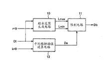
图17是表示基于实施方式4的像素插值电路的结构的图。该像素插值电路具有:多个平均维持插值运算电路6(1)至6(n-1)、即第一平均维持插值运算电路6(1)、第二平均维持插值运算电路6(2)、…、第n-1平均维持插值运算电路6(n-1)。这些平均维持插值运算电路6(1)至6(n-1)将参数k或从参数k中减去了i的(k-i)设定为互不相同的值。例如,对第一平均维持插值运算电路6(1)输入参数k=2,同样对第二平均维持插值运算电路6(2)、…、第n-1平均维持插值运算电路6(n-1)分别输入并设定k=3、…、kn。FIG. 17 is a diagram showing a configuration of a pixel interpolation circuit according to
输出电路5例如基于选择信号C,选择由多个平均维持插值运算电路6(1)至6(n-1)分别输出的插值数据中的一个,输出作为缺失像素的数据。The
图18是表示在实施方式1所示的包含缺失像素的像素列和不包含缺失像素的像素列不重复的情况下的k=kj的平均维持插值运算电路中,像素周期和插值误差之间的关系的曲线图。横轴Pp表示有周期性的图像数据的像素周期,纵轴E表示插值误差。FIG. 18 shows the relationship between the pixel period and the interpolation error in the k=kj average maintenance interpolation operation circuit in the case where the pixel row including the missing pixel and the pixel row not including the missing pixel shown in
说明k=kj的平均维持插值运算电路中的像素周期和插值误差之间的关系。The relationship between the pixel period and the interpolation error in the average maintenance interpolation operation circuit of k=kj will be described.
如实施方式1所示,包含缺失像素的像素列和不包含缺失像素的像素列不重复的情况下的平均维持插值运算电路在参数k为像素周期Pp的整数倍(k=N*Pp)的情况下,可以适当地对缺失像素进行插值。As shown in
从而,如图18所示,包含缺失像素的像素列和不包含缺失像素的像素列不重复的情况下的k=kj的平均维持插值运算电路在对像素周期Pp为Pp=kj/Na1、kj/Na2、…、kj(Na1>Na2>…>0、Na1、Na2、…是kj的约数)的图像数据进行插值时,插值误差E为0或最小。此外,待插值的图像数据的像素周期Pp越偏离Pp=kj/Na1、kj/Na2、…、kj的像素周期Pp,则插值误差E越大。Therefore, as shown in FIG. 18 , the k=kj average maintenance interpolation operation circuit in the case where the pixel row including the missing pixel and the pixel row not including the missing pixel do not overlap is Pp=kj/Na1, kj for the pixel period Pp. When the image data of /Na2, ..., kj (Na1>Na2>...>0, Na1, Na2, ... are divisors of kj) is interpolated, the interpolation error E is 0 or the minimum. In addition, the more the pixel period Pp of the image data to be interpolated deviates from the pixel period Pp of Pp=kj/Na1, kj/Na2, . . . , kj, the greater the interpolation error E will be.
图19是表示在包含缺失像素的像素列和不包含缺失像素的像素列不重复的情况下的k=2、3、4、kn-1、kn的平均维持插值运算电路中,像素周期和插值误差之间的关系的曲线图。图19(a)表示k=2的平均维持插值运算电路中的像素周期和插值误差之间的关系,图19(b)表示k=3的平均维持插值运算电路中的像素周期和插值误差之间的关系,图19(c)表示k=4的平均维持插值运算电路中的像素周期和插值误差之间的关系,图19(d)表示k=kn-1的平均维持插值运算电路中的像素周期和插值误差之间的关系,图19(e)表示k=kn的平均维持插值运算电路中的像素周期和插值误差之间的关系。Fig. 19 shows that in the average maintenance interpolation operation circuit of k=2, 3, 4, kn-1, kn under the condition that the pixel column including the missing pixel and the pixel column not including the missing pixel do not overlap, the pixel cycle and the interpolation A graph of the relationship between errors. Fig. 19 (a) shows the relationship between the pixel cycle and the interpolation error in the average maintenance interpolation operation circuit of k=2, and Fig. 19 (b) shows the relationship between the pixel cycle and the interpolation error in the average maintenance interpolation operation circuit of k=3. Figure 19(c) shows the relationship between the pixel cycle and the interpolation error in the average maintenance interpolation circuit of k=4, and Figure 19(d) shows the average maintenance interpolation circuit of k=kn-1 Regarding the relationship between the pixel period and the interpolation error, FIG. 19(e) shows the relationship between the pixel period and the interpolation error in the average maintenance interpolation operation circuit of k=kn.
说明k=2、3、4、kn-1、kn的平均维持插值运算电路中的像素周期和插值误差之间的关系。The relationship between the pixel period and the interpolation error in the average maintenance interpolation operation circuit of k=2, 3, 4, kn-1, kn will be described.
k=2的平均维持插值运算电路的参数k是素数,所以仅在Pp=2的图像数据中,插值误差E为0或最小。关于k=3的平均维持插值运算电路也同样,仅在Pp=3的图像数据中,插值误差E为0或最小。关于k=4的平均维持插值运算电路,如图18所示,在作为参数k=4的约数的Pp=2的图像数据和Pp=4的图像数据中,插值误差E为0或最小,但为了简单地表现曲线图,在曲线图中仅示出Pp=4附近的特性。关于k=kn-1的平均维持插值运算电路也与k=4的平均维持插值运算电路同样,在曲线图中仅示出Pp=kn-1附近的特性。关于k=kn的平均维持插值运算电路也同样,在曲线图中仅示出Pp=kn附近的特性。The parameter k of the average maintaining interpolation operation circuit of k=2 is a prime number, so only in the image data of Pp=2, the interpolation error E is 0 or the smallest. The same applies to the average maintaining interpolation circuit for k=3, and the interpolation error E is 0 or the smallest only in the image data of Pp=3. Regarding the average maintenance interpolation operation circuit of k=4, as shown in FIG. 18, in the image data of Pp=2 and the image data of Pp=4 which are divisors of the parameter k=4, the interpolation error E is 0 or the smallest, However, in order to simplify the presentation of the graph, only the characteristics around Pp=4 are shown in the graph. The average maintaining interpolation circuit for k=kn−1 is similar to the average maintaining interpolation circuit for k=4, and only the characteristics around Pp=kn−1 are shown in the graph. The same is true for the average maintaining interpolation operation circuit for k=kn, and only the characteristics around Pp=kn are shown in the graph.
图20是表示在包含缺失像素的像素列和不包含缺失像素的像素列不重复的k=2~k=kn的平均维持插值运算电路中、像素周期和插值误差之间的关系的曲线图、以及示出各个平均维持插值运算电路产生好结果的(可以以比较小的误差进行插值)像素周期Pp的范围的图。图20(a)表示将图19(a)~图19(e)的五个曲线重叠在一个坐标轴上的曲线图。图20(b)是表示各个平均维持插值运算电路的插值误差为最小的范围的图。R2表示k=2的平均维持插值运算电路的插值误差为最小的范围。R3~Rn表示k=3~k=kn的平均维持插值运算电路的插值误差分别为最小的范围。图20(c)表示k=2~k=kn的平均维持插值运算电路分别得到好结果的像素周期Pp的范围。20 is a graph showing the relationship between the pixel period and the interpolation error in an average maintaining interpolation operation circuit of k=2 to k=kn in which a pixel row including a missing pixel and a pixel row not including a missing pixel overlap, And a graph showing the range of the pixel period Pp in which each average-maintaining interpolation operation circuit produces a good result (interpolation can be performed with a relatively small error). FIG. 20( a ) shows a graph in which the five curves of FIGS. 19( a ) to 19( e ) are superimposed on one coordinate axis. FIG. 20( b ) is a diagram showing the range in which the interpolation error of each average maintenance interpolation operation circuit is the smallest. R2 represents the range where k=2 average maintains the interpolation error of the interpolation operation circuit to be the smallest. R3 to Rn represent the ranges in which the interpolation error of the average maintenance interpolation operation circuit of k=3 to k=kn is the smallest, respectively. FIG. 20( c ) shows the range of the pixel period Pp in which the average maintenance interpolation operation circuit of k=2~k=kn obtains good results respectively.
说明k=2~k=kn的平均维持插值运算电路分别得到好结果的像素周期。The average maintenance interpolation operation circuits of k=2~k=kn will be described to obtain the pixel period of good results respectively.
k=2的平均维持插值运算电路的插值误差为最小的范围是从Pp的最小值到k=2的平均维持插值运算电路的曲线和k=3的平均维持插值运算电路的曲线交叉的点为止的范围(相当于图20(b)的R2)。k=3的平均维持插值运算电路的插值误差为最小的范围是从k=3的平均维持插值运算电路的曲线与k=2的平均维持插值运算电路的曲线交叉的点到与k=4的平均维持插值运算电路的曲线交叉的点为止的范围(相当于图20(b)的R3)。对于k=4、kn-1、kn的平均维持插值运算电路也同样,R4、Rn-1、Rn所示的范围为各个平均维持插值运算电路的插值误差成为最小的范围。The range in which the interpolation error of the average maintaining interpolation circuit of k=2 is minimum is from the minimum value of Pp to the point where the curve of the average maintaining interpolation circuit of k=2 and the curve of the average maintaining interpolation circuit of k=3 intersect. range (equivalent to R2 in Figure 20(b)). The range where the interpolation error of the average maintenance interpolation operation circuit of k=3 is minimum is from the point where the curve of the average maintenance interpolation operation circuit of k=3 intersects the curve of the average maintenance interpolation operation circuit of k=2 to the point with k=4 The range (corresponding to R3 in FIG. 20( b )) to the point where the curves of the interpolation calculation circuit intersect is maintained on average. The same applies to the average maintaining interpolation circuits of k=4, kn−1, kn, and the ranges indicated by R4, Rn−1, Rn are the ranges in which the interpolation error of each average maintaining interpolation circuit becomes minimum.
从而,如图20(c)所示,各个平均维持插值运算电路的插值误差为最小的范围成为各个平均维持插值运算电路得到好结果的像素周期Pp的范围。Therefore, as shown in FIG. 20(c), the range in which the interpolation error of each average-maintaining interpolation circuit is the smallest is the range of the pixel period Pp in which each average-maintaining interpolation circuit obtains a good result.
以下说明图17所示的像素插值电路的动作。The operation of the pixel interpolation circuit shown in FIG. 17 will be described below.
将输入图像DI输入给第一平均维持插值运算电路6(1)~第n-1平均维持插值运算电路6(n-1)。如上所述,例如将参数k=2输入给第一平均维持插值运算电路6(2)。同样,将参数k=3、…、kn分别输入给第二平均维持插值运算电路6(2)、…、第n-1平均维持插值运算电路6(n-1)。The input image DI is input to the first average maintaining interpolation operation circuit 6 ( 1 ) to the (n−1)th average maintenance interpolation operation circuit 6 ( n−1). As described above, for example, the parameter k=2 is input to the first mean-maintaining interpolation operation circuit 6 ( 2 ). Similarly, the parameters k=3, ..., kn are respectively input to the second average maintaining interpolation operation circuit 6(2), ..., and the n-1th average maintenance interpolation operation circuit 6(n-1).
第一平均维持插值运算电路6(1)基于输入图像DI以及参数k=2,输出缺失像素的插值数据D1。第二平均维持插值运算电路6(2)、…、第n-1平均维持插值运算电路6(n-1)也同样基于输入图像DI以及参数k=3、…、kn,分别输出缺失像素的插值数据D2~Dn-1。将插值数据D1~Dn-1输入给输出电路5。将例如后述那样生成的选择信号C输入给输出电路5。输出电路5基于选择信号C选择插值数据D1~Dn-1中的一个,输出作为缺失像素的插值数据DO。The first average maintaining interpolation operation circuit 6 ( 1 ) outputs the interpolation data D1 of missing pixels based on the input image DI and the parameter k=2. The second average maintenance interpolation operation circuit 6(2), ..., and the n-1th average maintenance interpolation operation circuit 6 (n-1) are also based on the input image DI and parameters k=3, ..., kn, respectively output missing pixel Interpolation data D2 to Dn-1. The interpolation data D1 to Dn-1 are input to the
图17所示的像素插值电路具有多个参数不同的平均维持插值运算电路,从而可以实现图20(b)的插值误差的特性,所以如图20(c)所示,可以应用于从小的周期的图像数据到大的周期的图像数据的宽范围。The pixel interpolation circuit shown in Figure 17 has multiple average maintenance interpolation circuits with different parameters, so that the characteristics of the interpolation error in Figure 20(b) can be realized, so as shown in Figure 20(c), it can be applied to a small cycle A wide range of image data to large cycle image data.
实施方式5
图21表示基于实施方式5的像素插值电路的结构。FIG. 21 shows the configuration of a pixel interpolation circuit according to the fifth embodiment.
该像素插值电路除了图17的结构外还具有左右平均插值运算电路6(0)。平均维持插值运算电路6(1)至6(m-1)与图17的平均维持插值运算电路6(1)至6(n-1)是同样的,设有m-1个。该m可以是与图17的结构的n相同的值,也可以采用如后述的小于n的值。换言之,在设置左右平均插值运算电路6(0)的情况下,可以减少平均维持插值运算电路的数量。This pixel interpolation circuit has a left and right average interpolation operation circuit 6(0) in addition to the configuration shown in FIG. 17 . The average maintaining interpolation operation circuits 6(1) to 6(m-1) are the same as the average maintenance interpolation operation circuits 6(1) to 6(n-1) in FIG. 17, and m-1 are provided. This m may be the same value as n in the configuration of FIG. 17 , or a value smaller than n as described later may be used. In other words, when the left and right average interpolation operation circuits 6(0) are provided, the number of average maintenance interpolation operation circuits can be reduced.
左右平均插值运算电路6(0)生成位于缺失像素的左右侧的邻接像素的值的平均值,作为插值数据。另外,这里提到的‘左右’表示在水平方向上排列一系列的像素而进行描绘时、位于缺失像素的左右侧,在将一系列的像素作为时序数据时,与此相当的是位于‘前后’。The left-right average interpolation operation circuit 6 ( 0 ) generates the average value of the values of adjacent pixels located on the left and right sides of the missing pixel as interpolation data. In addition, the "left and right" mentioned here means that when a series of pixels are arranged in the horizontal direction and are drawn, they are located on the left and right sides of the missing pixel. '.
输出电路5例如基于选择信号(C),选择由所述多个平均维持插值运算电路6(1)至6(m-1)以及左右平均插值运算电路6(0)输出的插值数据中的一个,输出作为缺失像素的数据。The
图22是用于说明在像素周期Pp=2、3、4、kn的图像数据中,使用左右平均插值运算电路来对像素进行插值的方法的图。在图22中,示出了对周期变化的像素的极大值(各周期内的峰值)进行插值的情况。在由左右平均插值运算电路进行插值的情况下,在如图所示的极大值的插值的情况下,误差为最大。从而,如果对于极大值研究误差,则成为研究最大误差。FIG. 22 is a diagram for explaining a method of interpolating pixels using a left-right average interpolation calculation circuit in image data of pixel periods Pp=2, 3, 4, kn. In FIG. 22 , the case of interpolating the maximum value (peak value in each period) of a pixel that changes periodically is shown. In the case of interpolation by the left and right average interpolation calculation circuit, the error becomes the largest in the case of the interpolation of the maximum value as shown in the figure. Therefore, if the error is studied for the maximum value, the maximum error is studied.
图22(a)是表示像素周期Pp=2的图像数据的波形图,图22(b)是表示像素周期Pp=3的图像数据的波形图,图22(c)是表示像素周期Pp=4的图像数据的波形图,图22(d)是表示像素周期Pp=kn的图像数据的波形图。在各个波形图中L表示要插值的缺失像素,LL表示与缺失像素L左邻的像素,LR表示与缺失像素L右邻的像素,LA表示由左右平均插值运算电路生成的插值数据,E2~En分别表示插值数据和原始数据之间的误差。Fig. 22(a) is a waveform diagram representing the image data of the pixel period Pp=2, Fig. 22(b) is a waveform diagram representing the image data of the pixel period Pp=3, and Fig. 22(c) is a waveform diagram representing the pixel period Pp=4 Fig. 22(d) is a waveform diagram of image data representing a pixel period Pp=kn. In each waveform diagram, L represents the missing pixel to be interpolated, LL represents the pixel adjacent to the left of the missing pixel L, LR represents the pixel adjacent to the right of the missing pixel L, LA represents the interpolation data generated by the left and right average interpolation circuit, E2~ En represent the error between the interpolated data and the original data, respectively.
说明像素周期Pp=2、3、4、kn的图像数据中的左右平均插值运算电路的插值误差。The interpolation error of the left and right average interpolation calculation circuit in the image data of the pixel period Pp=2, 3, 4, kn will be described.
如图22(a)~图22(d)所示,左右平均插值运算电路将与缺失像素L左邻的像素LL和与缺失像素右邻的像素LR的平均值作为缺失像素L的插值数据LA。插值数据LA为As shown in Fig. 22(a) to Fig. 22(d), the left and right average interpolation operation circuit uses the average value of the pixel LL adjacent to the left of the missing pixel L and the pixel LR adjacent to the right of the missing pixel L as the interpolation data LA of the missing pixel L . The interpolated data LA is
LA=(LL+LR)/2。LA=(LL+LR)/2.
此外,在各个波形图中,插值数据LA和缺失像素L的原始数据之差为插值误差E2~En。In addition, in each waveform diagram, the difference between the interpolation data LA and the original data of the missing pixel L is the interpolation errors E2 to En.
在各个图像中对极大值进行插值的情况下,像素周期Pp越大则插值误差越小。在图23中示出左右平均插值运算电路中的像素周期和插值误差之间的关系。When interpolating the maximum value in each image, the larger the pixel period Pp, the smaller the interpolation error. FIG. 23 shows the relationship between the pixel period and the interpolation error in the left-right average interpolation operation circuit.
图24是表示在平均维持插值运算电路中像素周期和插值误差之间的关系的曲线图,以及示出k=2~kn的平均维持插值运算电路和左右平均插值运算电路得到好结果的像素周期Pp的范围的图。Fig. 24 is a graph showing the relationship between the pixel cycle and the interpolation error in the average maintaining interpolation operation circuit, and the pixel cycle showing that the average maintenance interpolation operation circuit and the left and right average interpolation operation circuits of k=2∼kn give good results Graph of the range of Pp.
说明左右平均插值运算电路得到好结果的像素周期Pp的范围。Explain the range of the pixel period Pp in which the left and right average interpolation operation circuit obtains good results.
图24(a)是表示图23所示的左右平均插值运算电路中的像素周期和插值误差之间的关系的曲线图。FIG. 24( a ) is a graph showing the relationship between the pixel period and the interpolation error in the left-right average interpolation calculation circuit shown in FIG. 23 .
Ep表示视觉辨认上可以允许的误差的上限值。Ep represents the upper limit value of the allowable error in visual recognition.
如图24(a)所示,左右平均插值运算电路是:像素周期Pp越大则插值误差E越小,所以在Pp=km+1~kn的图像数据中,插值误差E小于视觉辨认上可以允许的误差的上限值Ep。从而,在Rave所示的范围、即Pp=km+1~kn的图像数据中,可以将左右平均插值运算电路用于缺失像素的插值。As shown in Figure 24(a), the left and right average interpolation operation circuit is: the larger the pixel period Pp is, the smaller the interpolation error E is, so in the image data of Pp=km+1~kn, the interpolation error E is smaller than the visual recognition. The upper limit value Ep of the allowable error. Therefore, in the range indicated by Rave, that is, the image data of Pp=km+1 to kn, the left and right average interpolation calculation circuit can be used for interpolation of missing pixels.
图24(b)表示图20(c)所示的k=2~k=kn的平均维持插值运算电路得到好结果的像素周期Pp的范围。如图24(a)所示,在Pp=km+1~kn的图像数据中,可以将左右平均插值运算电路用于缺失像素的插值,所以可以使用左右平均插值运算电路的输出来代替图17的参数k=km+1~kn(假设m<n)的平均维持插值运算电路的输出。从而,可以省略参数k=km+1~kn(假设m<n)的平均维持插值运算电路。FIG. 24(b) shows the range of the pixel period Pp in which the average maintenance interpolation circuit of k=2 to k=kn shown in FIG. 20(c) obtains a good result. As shown in Figure 24(a), in the image data of Pp=km+1~kn, the left and right average interpolation circuit can be used for the interpolation of missing pixels, so the output of the left and right average interpolation circuit can be used instead of the output of Figure 17 The average of the parameter k=km+1~kn (assuming m<n) maintains the output of the interpolation operation circuit. Therefore, an average maintaining interpolation operation circuit for the parameter k=km+1∼kn (assuming m<n) can be omitted.
通过将图17的结构中的k=km+1~kn的平均维持插值运算电路置换为左右平均插值运算电路,可以削减平均维持插值运算电路的种类。从而,可以缩小可应用于宽范围的像素周期的像素插值电路的电路规模。By replacing the average maintaining interpolation operation circuits of k=km+1 to kn in the configuration of FIG. 17 with left and right average interpolation operation circuits, the types of average maintenance interpolation operation circuits can be reduced. Thus, the circuit scale of the pixel interpolation circuit applicable to a wide range of pixel periods can be reduced.
此外,由左右平均插值运算电路和多个插值运算电路构成的像素插值电路具有如图25所示的插值误差的特性。图25与图20(b)所示的曲线图同样,在R2中,k=2的平均维持插值运算电路的插值误差为最小,同样在R3~Rm中,k=3~km的平均维持插值运算电路的插值误差分别为最小。在Rave中,左右平均插值运算电路的插值误差为最小。In addition, a pixel interpolation circuit composed of a left-right average interpolation operation circuit and a plurality of interpolation operation circuits has interpolation error characteristics as shown in FIG. 25 . Fig. 25 is the same as the graph shown in Fig. 20(b). In R2, the interpolation error of the average maintaining interpolation operation circuit of k=2 is the minimum. Similarly, in R3~Rm, the average maintaining interpolation of k=3~km The interpolation errors of the arithmetic circuits were minimal. In Rave, the interpolation error of the left and right average interpolation operation circuits is the smallest.
图26是表示在实施方式2以及实施方式3所示的包含缺失像素的像素列和不包含缺失像素的像素列重复i像素的情况下的k=kj的平均维持插值运算电路中,像素周期Pp和插值误差之间的关系的曲线图。FIG. 26 shows the pixel period Pp in an average maintaining interpolation operation circuit of k=kj in the case where i pixels are overlapped between a pixel row including a missing pixel and a pixel row not including a missing pixel shown in
说明像素周期和插值误差之间的关系。Illustrates the relationship between pixel period and interpolation error.
如实施方式2以及实施方式3所示,包含缺失像素的像素列和不包含缺失像素的像素列重复i像素的情况下的平均维持插值运算电路是:在参数k为像素周期Pp的整数倍(k=N*Pp),或包含缺失像素的像素列和不包含缺失像素的像素列不重复的的部分的像素个数k-i为像素周期Pp的整数倍(k-i=N*Pp)的情况下,可以适当地对缺失像素进行插值。As shown in
如图26(a)所示,包含缺失像素的像素列和不包含缺失像素的像素列重复i像素的情况下的k=kj的平均维持插值运算电路在对像素周期Pp为Pp=kj/Na1、…、kj(Na1>…>0、Na1、…是kj的约数)的图像数据进行插值的情况下,插值误差E为0或最小,待插值的图像数据的像素周期Pp越偏离Pp=kj/Na1、kj/Na2、…、kj的像素周期Pp,则插值误差E越大。As shown in FIG. 26(a), when i pixels are repeated between the pixel row including the missing pixel and the pixel row not including the missing pixel, the average maintenance interpolation operation circuit of k=kj is Pp=kj/Na1 for the pixel period Pp. , ..., kj (Na1 > ... > 0, Na1, ... are divisors of kj) image data under the situation of interpolation, the interpolation error E is 0 or the minimum, the pixel period Pp of the image data to be interpolated deviates from Pp= The pixel period Pp of kj/Na1, kj/Na2, ..., kj, the larger the interpolation error E is.
进而,如图26(b)所示,在对像素周期Pp为Pp=(kj-i)/Nb1、…、kj-i(Nb1>…>0、Nb1、…是kj-i的约数)的图像数据进行插值的情况下,插值误差E也为0或最小,像素周期Pp越偏离Pp=(kj-i)/Nb1、…、kj-i的像素周期Pp,则插值误差E越大。Furthermore, as shown in FIG. 26(b), when the pixel period Pp is Pp=(kj-i)/Nb1,...,kj-i (Nb1>...>0, Nb1,...is a divisor of kj-i) In the case of image data interpolation, the interpolation error E is also 0 or the minimum, and the more the pixel period Pp deviates from the pixel period Pp of Pp=(kj-i)/Nb1,...,kj-i, the larger the interpolation error E is.
从而,包含缺失像素的像素列和不包含缺失像素的像素列重复i像素的情况下的平均维持插值运算电路中的像素周期Pp和插值像素之间的关系,成为将图26(a)的曲线和图26(b)的曲线结合而得到的图26(c)的曲线图。Therefore, when the pixel column including the missing pixel and the pixel column not including the missing pixel overlap i pixels, the average maintains the relationship between the pixel period Pp in the interpolation operation circuit and the interpolation pixel, which becomes the curve of FIG. 26(a) The graph of FIG. 26(c) obtained by combining with the graph of FIG. 26(b).
图27是表示在实施方式3所示的由包含缺失像素的像素列和不包含缺失像素的两个像素列实现的平均维持插值运算电路中,包含缺失像素的像素列LC和不包含缺失像素的像素列NA以及NB之间的位置关系的一例。图27(a)表示k=3、i=1的情况下的包含缺失像素的像素列LC和不包含缺失像素的像素列NA以及NB之间的位置关系。图27(b)表示k=5、i=2的情况下的包含缺失像素的像素列LC和不包含缺失像素的像素列NA以及NB之间的位置关系。图27(c)表示k=kn、i=(kn-1)/2的情况下的包含缺失像素的像素列LC和不包含缺失像素的像素列NA以及NB之间的位置关系。FIG. 27 is a diagram showing the average maintenance interpolation operation circuit realized by the pixel column including the missing pixel and the two pixel columns not including the missing pixel shown in the third embodiment, the pixel column LC including the missing pixel and the pixel column not including the missing pixel. An example of the positional relationship between the pixel rows NA and NB. FIG. 27( a ) shows the positional relationship between the pixel column LC including the missing pixel and the pixel columns NA and NB not including the missing pixel when k=3 and i=1. FIG. 27( b ) shows the positional relationship between the pixel column LC including the missing pixel and the pixel columns NA and NB not including the missing pixel when k=5 and i=2. FIG. 27( c ) shows the positional relationship between the pixel column LC including missing pixels and the pixel columns NA and NB not including missing pixels when k=kn and i=(kn−1)/2.
说明在图27所示的包含缺失像素的像素列和不包含缺失像素的两个像素列所实现的平均维持插值运算电路中,参数k以及i和可以适当地进行插值的图像数据的像素周期Pp之间的关系。The parameters k and i and the pixel period Pp of the image data that can be properly interpolated in the average maintaining interpolation operation circuit realized by the pixel column including the missing pixel and the two pixel columns not including the missing pixel shown in FIG. 27 will be described. The relationship between.
如图26所示,包含缺失像素的像素列和不包含缺失像素的像素列重复i像素的k=kj的平均维持插值运算电路可以适当地对像素周期Pp为Pp=kj/Na1、…、kj的图像数据或Pp=(kj-i)/Nb1、…、kj-i的图像进行插值,所以图27(a)所示的包含缺失像素的像素列和不包含缺失像素的两个像素列重复1像素的k=3的平均维持插值运算电路对于Pp=k=3或Pp=k-i=2的图像数据可以适当地进行插值。As shown in FIG. 26 , the average maintaining interpolation operation circuit of k=kj of repeated i pixels in the pixel row including the missing pixel and the pixel row not including the missing pixel can be suitably Pp=kj/Na1, . . . , kj for the pixel period Pp. The image data of Pp=(kj-i)/Nb1,...,kj-i are interpolated, so the pixel column containing missing pixels and the two pixel columns not containing missing pixels shown in Figure 27(a) are repeated The k=3 average maintaining interpolation operation circuit for 1 pixel can appropriately perform interpolation for image data of Pp=k=3 or Pp=k−i=2.
关于图27(b)所示的包含缺失像素的像素列和不包含缺失像素的两个像素列重复2像素的k=5的平均维持插值运算电路也同样,对于Pp=k=5或Pp=k-i=3的图像数据可以适当地进行插值。The same is true for the average maintenance interpolation operation circuit of k=5 that repeats 2 pixels for the pixel row including the missing pixel and the two pixel rows not including the missing pixel shown in FIG. 27( b ). Image data of k-i=3 can be properly interpolated.
关于图27(c)所示的包含缺失像素的像素列和不包含缺失像素的像素列重复(kn-1)/2个像素的k=kn的平均维持插值运算电路也同样,对于Pp=kn/Na1、…、kn的图像数据或Pp=(kn-i)/Nb1、…、kn-i的图像数据可以适当地进行插值。The same is true for the average maintaining interpolation operation circuit of k=kn in which the pixel row including the missing pixel and the pixel row not including the missing pixel shown in FIG. 27(c) repeat (kn-1)/2 pixels. The image data of /Na1, . . . , kn or the image data of Pp=(kn-i)/Nb1, . . . , kn-i can be appropriately interpolated.
图28是表示在图27所示的包含缺失像素的像素列和不包含缺失像素的两个像素列重复的情况下的平均维持插值运算电路中,各个平均维持插值运算电路得到好结果的像素周期Pp的范围的图。FIG. 28 is a graph showing the pixel cycle in which each average-maintaining interpolation circuit obtains a good result in the average-maintaining interpolation circuit in the case where the pixel column including the missing pixel and the two pixel columns not including the missing pixel overlap shown in FIG. 27 Graph of the range of Pp.
k=3的平均维持插值运算电路将Pp=3附近的像素周期Pp设为得到好结果的像素周期的范围。关于k=5的平均维持插值运算电路也同样,将Pp=5附近的像素周期Pp设为得到好结果的像素周期的范围。关于k=(kn+1)/2、kn的平均维持插值运算电路也同样,将Pp=(kn+1)/2、kn附近的像素周期Pp分别设为得到好结果的像素周期的范围。从而,k=3、5、(kn+1)/2、kn的平均维持插值运算电路分别得到好结果的像素周期的范围如图28(a)这样。The average maintenance interpolation circuit of k=3 sets the pixel period Pp around Pp=3 as the range of the pixel period in which a good result is obtained. The same applies to the average maintenance interpolation circuit for k=5, and the pixel period Pp around Pp=5 is set as the range of the pixel period in which a good result is obtained. The average maintenance interpolation circuit for k=(kn+1)/2, kn is similarly set to Pp=(kn+1)/2, and the pixel period Pp around kn is the range of the pixel period for which good results are obtained. Therefore, the ranges of pixel periods in which the average maintenance interpolation circuits of k=3, 5, (kn+1)/2, and kn respectively obtain good results are as shown in Fig. 28(a).
进而,k=3的平均维持插值运算电路的Pp=k-i=2附近的像素周期Pp也为得到好结果的像素周期的范围。关于k=5的平均维持插值运算电路也同样,将Pp=k-i=3附近的像素周期Pp设为得到好结果的像素周期的范围。关于k=7、9、kn的平均维持插值运算电路也同样,将Pp=4、5、(kn+1)/2附近的像素周期Pp分别设为得到好结果的像素周期的范围。从而,k=3、5、7、9、(kn+1)/2的平均维持插值运算电路分别得到好结果的像素周期的范围如图28(b)这样。Furthermore, the pixel period Pp around Pp=k-i=2 in the average maintaining interpolation circuit of k=3 is also the range of the pixel period in which good results are obtained. The average maintenance interpolation circuit for k=5 also sets the pixel period Pp around Pp=k-i=3 as the range of the pixel period in which a good result is obtained. The average maintenance interpolation circuit for k=7, 9, and kn is also similarly set to the pixel cycle Pp around Pp=4, 5, (kn+1)/2, respectively, as the range of the pixel cycle in which good results are obtained. Therefore, the average maintaining interpolation operation circuits of k=3, 5, 7, 9, (kn+1)/2 respectively obtain good results in the range of the pixel cycle as shown in Fig. 28(b).
从而,包含缺失像素的像素列和不包含缺失像素的两个像素列重复的情况下的k=3、5、(kn+1)/2、kn的平均维持插值运算电路可以应用于图28(a)和图28(b)合起来的范围、即如图28(c)所示的范围的图像数据。Therefore, k=3, 5, (kn+1)/2, kn average maintenance interpolation operation circuit of k=3, 5, (kn+1)/2, kn can be applied to FIG. 28 ( a) Image data of the combined range of FIG. 28( b ), that is, the range shown in FIG. 28( c ).
这样,对多个平均维持插值运算电路加上左右平均插值运算电路,选择它们生成的插值数据中、插值误差最小的数据,由此可以在与像素周期无关的情况下始终输出插值误差小的插值数据。In this way, by adding left and right average interpolation circuits to a plurality of average-maintaining interpolation circuits and selecting the interpolation data generated by them with the smallest interpolation error, it is possible to always output an interpolation value with a small interpolation error regardless of the pixel period. data.
实施方式6
图29是表示实施方式6中的像素插值电路的结构的图。FIG. 29 is a diagram showing the configuration of a pixel interpolation circuit in
实施方式6中的像素插值电路除了实施方式4所示的图21的结构之外,还具有生成输入给输出电路的选择信号的选择信号生成部9、控制电路20、以及图像数据存储器21。The pixel interpolation circuit in
图像数据存储器21暂时存储输入图像数据DI,按照来自控制电路20的指示,重复输出相同的图像数据。The
选择信号生成部9基于缺失像素附近的像素的原始数据、以及对该缺失像素附近的像素、通过与求出缺失像素的插值数据相同的方法而求得的插值数据,生成选择来自多个插值运算电路的插值数据中的一个的选择信号C。The
图示的选择信号生成部9由管理电路7以及评分电路8构成。The illustrated
多个平均维持插值运算电路6(1)至6(n)分别例如图16所示,更具体地如图1所示那样构成。A plurality of mean-maintaining interpolation calculation circuits 6(1) to 6(n) are configured as shown in FIG. 16, more specifically, as shown in FIG. 1, respectively.
控制电路20对多个平均维持插值运算电路6(1)至6(n)各自的、例如缺失部合计计算电路19(图16)输入构成包含缺失像素附近的测试用非缺失像素的像素组的k个像素中、测试用非缺失像素以外的像素,求出其值的合计SL,对多个插值运算电路各自的、非缺失部合计计算电路17输入构成不包含测试用缺失像素的像素组的k个像素,求出其值的合计,使多个插值运算电路各自的差分电路3通过从非缺失部合计计算电路17的输出中减去缺失部合计计算电路19的输出来求出测试用非缺失像素的插值数据。The
控制电路20还对左右平均插值运算电路6(0)输入位于缺失像素附近的测试用非缺失像素的左右侧的像素,求出其值的平均,将其作为测试用非缺失像素的插值数据输出。The
控制电路20对于多个互不相同的测试用非缺失像素进行这样的处理。The
选择信号生成部9基于由多个插值运算电路分别求出的测试用非缺失像素的插值数据、以及测试用非缺失像素的原始数据,对插值运算电路进行评价,确定选择信号的内容,使得选择得到最佳评价的插值运算电路。The selection
控制电路20对多个平均维持插值运算电路6(1)至6(n)的缺失部合计计算电路19输入构成包含缺失像素的像素组的像素,对非缺失部合计计算电路输入构成不包含缺失像素的像素组的像素,使其分别进行对于缺失像素的平均维持插值运算,对左右平均插值运算电路6(0)输入与缺失像素邻接的像素,使其进行对于缺失像素的左右平均插值运算,使输出电路5基于如上所述确定了内容的选择信号C,选择来自多个插值运算电路6(0)至6(n)的插值数据中的一个并输出。The
另外,在图29中,为了便于说明,平均维持插值运算电路的数量与图17以及图21的情况不同,图示出n个。In addition, in FIG. 29 , for convenience of explanation, the number of average maintenance interpolation calculation circuits is different from that in FIG. 17 and FIG. 21 , and n is shown in the figure.
图29的像素插值电路在每次提供了输入图像数据时,如下地进行两种处理。The pixel interpolation circuit in FIG. 29 performs two types of processing as follows every time input image data is supplied.
首先,第一处理也被称为评价处理,使用所提供的输入图像数据中的缺失像素以外的像素进行多个插值运算电路的评价,根据哪个插值运算电路得到了最佳的评价来确定选择信号C的内容。First, the first process is also referred to as evaluation process, and evaluates a plurality of interpolation calculation circuits using pixels other than missing pixels in the supplied input image data, and determines a selection signal based on which interpolation calculation circuit has obtained the best evaluation. the content of C.
第二处理也称为插值执行处理,基于选择信号C的内容,生成对所提供的输入图像数据中的缺失像素进行插值的插值数据,进行插值。The second processing is also referred to as interpolation execution processing, and based on the contents of the selection signal C, interpolation data for interpolating missing pixels in the supplied input image data is generated and interpolated.
由于在评价处理以及插值执行处理中重复使用相同的输入图像数据DI,因此输入图像数据DI暂时存储在图像数据存储器21中,然后根据来自控制电路20的指示重复进行读取。Since the same input image data DI is repeatedly used in the evaluation process and the interpolation execution process, the input image data DI is temporarily stored in the
评价处理中的插值运算和插值执行处理中的插值运算可以同时并行地进行,或也可以在评价处理中的插值运算结束后进行插值执行处理中的插值运算。以下,最先,作为评价处理中的插值运算和插值执行处理中的插值运算同时并行地进行的情况说明概略,然后,对于评价处理中的插值运算结束后进行插值执行处理中的插值运算的情况详细地进行说明。The interpolation calculation in the evaluation process and the interpolation calculation in the interpolation execution process may be performed in parallel at the same time, or the interpolation calculation in the interpolation execution process may be performed after the interpolation calculation in the evaluation process is completed. Hereinafter, first, an outline will be described as a case where the interpolation calculation in the evaluation process and the interpolation calculation in the interpolation execution process are performed in parallel at the same time, and then the case where the interpolation calculation in the interpolation execution process is performed after the interpolation calculation in the evaluation process is completed It demonstrates in detail.
输入图像DI输入给左右平均插值运算电路6(0)以及n个平均维持插值运算电路(第一平均维持插值运算电路6(1)、第二平均维持插值运算电路6(2)、…、第n平均维持插值运算电路6(n))以及评分电路8。平均维持插值运算电路的参数k=k1~kn分别输入到第一平均维持插值运算电路~第n平均维持插值运算电路中。左右平均插值运算电路6(0)基于输入图像数据DI,输出关于多个测试用非缺失像素(测试像素)的插值数据(测试插值数据)TD0[T1]~[Tm]和缺失像素的插值数据D0。从左右平均插值运算电路6(0)中输出的测试插值数据TD0[T1]~[Tm]输入到评分电路8中,插值数据D1D0被输入给输出电路5。The input image DI is input to the left and right average interpolation operation circuit 6 (0) and n average maintenance interpolation operation circuits (the first average maintenance interpolation operation circuit 6 (1), the second average maintenance interpolation operation circuit 6 (2), ..., the first average maintenance interpolation operation circuit 6 (2), ..., The n average maintains the interpolation operation circuit 6 (n)) and the
第一平均维持插值运算电路6(1)基于输入图像DI以及参数k=k1,输出关于多个测试像素的插值数据TD1[T1]~[Tm]和缺失像素的插值数据D1。从第一平均维持插值运算电路6(1)中输出的测试插值数据TD1[T1]~[Tm]被输入给评分电路8,插值数据D1被输入给输出电路5。The first average maintaining interpolation operation circuit 6(1) outputs interpolation data TD1[T1]˜[Tm] for a plurality of test pixels and interpolation data D1 for missing pixels based on the input image DI and the parameter k=k1. The test interpolation data TD1 [ T1 ] to [ Tm ] output from the first mean-maintaining interpolation operation circuit 6 ( 1 ) are input to the
关于第二平均维持插值运算电路6(2)~第n平均维持插值运算电路6(n)也同样,基于输入图像DI以及参数k=k2~k=kn,分别输出关于多个测试像素的插值数据TD2[T1]~[Tm]~TDn[T1]~[Tm]和缺失像素的插值数据D2~Dn。从第二平均维持插值运算电路6(2)~第n平均维持插值运算电路6(n)中输出的测试插值数据TD2[T1]~[Tm]~TDn[T1]~[Tm]被输入给评分电路8,插值数据D2~Dn被输入给输出电路5。The same applies to the second mean-maintaining interpolation circuit 6(2) to the n-th mean-maintaining interpolation circuit 6(n), based on the input image DI and parameters k=k2 to k=kn, respectively output interpolation values for a plurality of test pixels. Data TD2 [T1] to [Tm] to TDn [T1] to [Tm] and interpolation data D2 to Dn of missing pixels. The test interpolation data TD2[T1]~[Tm]~TDn[T1]~[Tm] output from the second average maintaining interpolation operation circuit 6(2) to the nth average maintenance interpolation operation circuit 6(n) are input to Scoring
评分电路8基于输入图像DI对从左右平均插值运算电路6(0)中输出的测试插值数据TD0进行评分,将其结果作为评分数据M0输出。从评分电路8中输出的评分数据M0输入给管理电路7。The
此外,评分电路8对于从第一平均维持插值运算电路6(1)~第n平均维持插值运算电路6(n)中输出的测试插值数据TD1[T1]~[Tm]~TDn[T1]~[Tm]也同样,基于输入图像DI进行评分,将各个结果作为评分数据M1~Mn输出。从评分电路8中输出的评分数据M1~Mn输入给管理电路7。In addition, the
管理电路7例如后述这样评价从评分电路8中输出的评分数据M0~Mn,基于其结果输出选择信号C。从管理电路7中输出的选择信号C输入给输出电路5。The
输出电路5基于从管理电路7中输出的选择信号C,选择左右平均插值运算电路6(0)以及第一平均维持插值运算电路6(1)~第n平均维持插值运算电路6(n)输出的插值数据D0~Dn中的一个,作为输出数据DO输出。Based on the selection signal C output from the
以下更详细地说明评价处理中的插值运算结束后进行插值执行处理中的插值运算的情况。The case where the interpolation calculation in the interpolation execution process is performed after the interpolation calculation in the evaluation process is completed will be described in more detail below.
首先对于评价处理的动作进行说明。此时,图29的输出电路5不工作。即,不输出插值数据DO。First, the operation of the evaluation process will be described. At this time, the
图30(a)是表示输入图像DI的图,表示缺失像素和测试用非缺失像素(测试像素)之间的位置关系。在图30中,○表示实际存在的像素,×表示缺失的像素。FIG. 30( a ) is a diagram showing the input image DI, and shows the positional relationship between missing pixels and non-missing pixels for testing (test pixels). In FIG. 30 , ○ indicates an actually existing pixel, and × indicates a missing pixel.
相对于缺失像素L,将T1~Tm所示的、位于缺失像素L附近的实际存在的像素(非缺失像素)确定为测试像素(假设m=2k)。这里,测试像素是指在缺失像素附近虚拟地视为缺失像素而生成插值数据的像素。图30(a)是以缺失像素L为中心一维地在左右两侧各设定了k个测试像素的例子。With respect to the missing pixel L, the actually existing pixels (non-missing pixels) indicated by T1 to Tm located near the missing pixel L (non-missing pixels) are determined as test pixels (assuming m=2k). Here, the test pixel refers to a pixel that is virtually regarded as a missing pixel near the missing pixel and generates interpolation data. FIG. 30( a ) is an example in which k test pixels are set one-dimensionally on the left and right sides of the missing pixel L as the center.
测试像素可以相对于缺失像素左右不均等地进行设定,也可以仅在左右一方进行设定。此外,也可以如图30(b)这样二维地进行设定。The test pixels may be set unevenly on the left and right relative to the missing pixels, or may be set only on the left and right sides. In addition, it can also be set two-dimensionally as shown in FIG. 30( b ).
使用图29以及图30(a)详细地说明测试像素T1~Tm中的左右平均插值运算电路6(0)、第一平均维持插值运算电路6(1)~第n平均维持插值运算电路6(n)以及评分电路8的动作。29 and FIG. 30( a ), the left and right average interpolation operation circuits 6 ( 0 ), the first average maintenance interpolation operation circuit 6 ( 1 ) to the nth average maintenance interpolation operation circuit 6 ( n) and the action of the
首先,在测试像素T1的位置处,左右平均插值运算电路6(0)输出将测试像素T1虚拟地视为缺失的情况下的测试插值数据TD0[T1]。即,求出位于测试像素T1的左右侧的像素的平均,将其作为测试像素T1的插值数据输出。First, at the position of the test pixel T1 , the left-right average interpolation operation circuit 6 ( 0 ) outputs test interpolation data TD0 [ T1 ] in the case where the test pixel T1 is virtually regarded as missing. That is, the average value of the pixels located on the left and right sides of the test pixel T1 is obtained and output as the interpolation data of the test pixel T1.
评分电路8求出测试像素T1的位置处的输入图像DI的数据DI[T1]和所述测试插值数据TD0[T1]的差分的绝对值,作为评分数据M0[T1]输出。评分数据M0[T1]成为The
M0[T1]=|TD0[T1]-DI[T1]|。M0[T1]=|TD0[T1]-DI[T1]|.
在评分数据M0[T1]小的情况下,表示测试插值数据接近输入图像,即,在测试像素T1中,左右平均插值运算电路6(0)的运算方法适当。反之,在评分数据M0[T1]大的情况下,表示在测试像素T1中,左右平均插值运算电路6(0)的运算方法不适当。换言之,评分数据M0[T1]表示测试像素T1中的左右平均插值运算电路6(0)的适当性。When the score data M0[T1] is small, it means that the test interpolation data is close to the input image, that is, the calculation method of the left and right average interpolation calculation circuit 6(0) is appropriate for the test pixel T1. Conversely, when the score data M0[T1] is large, it means that the calculation method of the left-right average interpolation calculation circuit 6(0) is not appropriate for the test pixel T1. In other words, the score data M0[T1] indicates the adequacy of the left-right average interpolation operation circuit 6(0) in the test pixel T1.
接着,左右平均插值运算电路6(0)关于测试像素T2也同样,输出将测试像素T2虚拟地视为缺失的情况下的测试插值数据TD0[T2]。评分电路8求出测试像素T2的位置处的输入图像DI[T2]和所述测试插值数据TD0[T2]的差分的绝对值,作为评分数据M0[T2]输出。评分数据M0[T2]成为Next, the left and right average interpolation calculation circuit 6 ( 0 ) similarly outputs test interpolation data TD0 [ T2 ] when the test pixel T2 is assumed to be missing in the same manner. The
M0[T2]=|TD0[T2]-DI[T2]|。M0[T2]=|TD0[T2]-DI[T2]|.
评分数据M0[T2]表示测试像素T2中的左右平均插值运算电路6(0)的适当性。The scoring data M0[T2] indicates the adequacy of the left and right average interpolation operation circuit 6(0) in the test pixel T2.
左右平均插值运算电路6(0)关于剩余的测试像素T3~Tm也同样地输出测试插值数据TD0[T3]~TD0[Tm]。评分电路8求出所述测试插值数据TD0[T3]~TD0[Tm]和与各个测试插值数据对应的输入图像DI的数据DI[T3]~DI[Tm]的差分的绝对值,作为评分数据M0[T3]~M0[Tm]输出。评分数据M0[T3]~M0[Tm]为The left and right average interpolation calculation circuit 6 ( 0 ) similarly outputs test interpolation data TD0 [ T3 ] to TD0 [Tm] for the remaining test pixels T3 to Tm. The
M0[T3]=|TD0[T3]-DI[T3]|M0[T3]=|TD0[T3]-DI[T3]|
~~
M0[Tm]=|TD0[Tm]-DI[Tm]|。M0[Tm]=|TD0[Tm]-DI[Tm]|.
评分数据M0[T3]~M0[Tm]表示测试像素T3~Tm中的左右平均插值运算电路6(0)的适当性。The scoring data M0 [T3] to M0 [Tm] indicate the appropriateness of the left and right average interpolation calculation circuits 6 ( 0 ) in the test pixels T3 to Tm.
这样,得到测试像素T1~Tm中的与左右平均插值运算电路6(0)所输出的测试插值数据对应的评分数据。In this way, score data corresponding to the test interpolation data output from the left-right average interpolation calculation circuit 6 ( 0 ) among the test pixels T1 to Tm is obtained.
对于第一平均维持插值运算电路6(1)也同样,在测试像素T1的位置处输出将测试像素T1虚拟地视为缺失的情况下的测试插值数据TD1[T1]。评分电路8求出测试像素T1的位置处的输入图像DI的数据DI[T1]和所述测试插值数据TD1[T1]之间的差分的绝对值,作为评分数据M1[T1]输出。评分数据M1[T1]成为Similarly, the first average maintenance interpolation calculation circuit 6 ( 1 ) outputs test interpolation data TD1 [ T1 ] at the position of the test pixel T1 when the test pixel T1 is assumed to be virtually missing. The
M1[T1]=|TD1[T1]-DI[T1]|。M1[T1]=|TD1[T1]-DI[T1]|.
评分数据M1[T1]表示测试像素T1中的第一平均维持插值运算电路6(1)的适当性。Score data M1[T1] indicates the adequacy of the first average-maintaining interpolation operation circuit 6(1) in the test pixel T1.
第一平均维持插值运算电路6(1)关于剩余的测试像素T2~Tm也同样地输出测试插值数据TD1[T2]~TD1[Tm]。评分电路8求出所述测试插值数据TD1[T2]~TD1[Tm]和与各个测试插值数据对应的输入图像DI的数据DI[T2]~DI[Tm]之间的差分的绝对值,作为评分数据M1[T2]~M1[Tm]输出。评分数据M1[T2]~M1[Tm]为The first average maintaining interpolation calculation circuit 6 ( 1 ) similarly outputs test interpolation data TD1 [ T2 ] to TD1 [Tm] for the remaining test pixels T2 to Tm. The
M1[T2]=|TD1[T2]-DI[T2]|M1[T2]=|TD1[T2]-DI[T2]|
~~
M1[Tm]=|TD1[Tm]-DI[Tm]|。M1[Tm]=|TD1[Tm]-DI[Tm]|.
评分数据M1[T2]~M1[Tm]表示测试像素T2~Tm中的第一平均维持插值运算电路6(1)的适当性。Score data M1 [ T2 ] to M1 [ Tm ] indicate the suitability of the first average maintenance interpolation operation circuit 6 ( 1 ) in the test pixels T2 to Tm.
关于第二平均维持插值运算电路6(2)~第n平均维持插值运算电路6(n)也同样,输出测试像素T1~Tm中的测试插值数据TD2[T1]…TD2[Tm]~TDn[T1]…TDn[Tm],评分电路8基于所述测试插值数据TD2[T1]…TD2[Tm]~TDn[T1]…TDn[Tm],分别输出评分数据M2[T1]…M2[Tm]~Mn[T1]…Mn[Tm]。The second average maintaining interpolation operation circuit 6 ( 2 ) to the n-th average maintenance interpolation operation circuit 6 ( n) also output test interpolation data TD2[T1]... TD2[Tm] to TDn[ in the test pixels T1 to Tm. T1]...TDn[Tm], scoring
这样,在所有的测试像素T1~Tm中,求出了左右平均插值运算电路6(0)以及第一平均维持插值运算电路6(1)~第n平均维持插值运算电路6(n)中的各个插值运算电路的适当性。In this way, in all the test pixels T1 to Tm, the left and right average interpolation operation circuit 6(0) and the first average maintenance interpolation operation circuit 6(1) to the n-th average maintenance interpolation operation circuit 6(n) are obtained. The appropriateness of each interpolation operation circuit.
图31是将测试像素T1~Tm中的各个插值运算电路的评分数据集中的表。FIG. 31 is a table that collects score data of each interpolation operation circuit in test pixels T1 to Tm.
通过使用测试像素的测试插值数据和测试像素的位置处的输入图像数据之间的差分的绝对值,可以对每个测试像素求出插值方法的适当性。The appropriateness of the interpolation method can be found for each test pixel by using the absolute value of the difference between the test interpolation data of the test pixel and the input image data at the position of the test pixel.
说明管理电路7的动作。The operation of the
为了评价缺失像素附近的左右平均插值运算电路6(0)的适当性,管理电路7将评分数据M0[T1]~M0[Tm]相加来生成左右平均插值运算电路6(0)的评价数据S0。评价数据S0为In order to evaluate the suitability of the left and right average interpolation operation circuit 6(0) in the vicinity of the missing pixel, the
S0=M0[T1]+M0[T2]+…+M0[Tm]。S0=M0[T1]+M0[T2]+...+M0[Tm].
在评价数据S0小的情况下,表示缺失像素附近的左右平均插值运算电路6(0)的运算方法适当。反之,在评价数据S0大的情况下,表示缺失像素附近的左右平均插值运算电路6(0)的运算方法不适当。When the evaluation data S0 is small, it indicates that the calculation method of the left and right average interpolation calculation circuit 6 ( 0 ) near the missing pixel is appropriate. Conversely, when the evaluation data S0 is large, it means that the calculation method of the left-right average interpolation calculation circuit 6 ( 0 ) in the vicinity of the missing pixel is not appropriate.
为了对第一平均维持插值运算电路6(1)~第n平均维持插值运算电路6(n)也同样评价缺失像素附近的适当性,管理电路7将评分数据M1[T1]…M1[Tm]~Mn[T1]…Mn[Tm]分别相加来分别生成第一平均维持插值运算电路6(1)~第n平均维持插值运算电路6(n)的评价数据S1~Sn。评价数据S1~Sn为In order to similarly evaluate the suitability of the vicinity of the missing pixel for the first average-maintaining interpolation operation circuit 6 ( 1 ) to the n-th average-maintenance interpolation operation circuit 6 ( n ), the
S1=M1[T1]+M1[T2]+…+M1[Tm]S1=M1[T1]+M1[T2]+…+M1[Tm]
~~
Sn=Mn[T1]+Mn[T2]+…+Mn[Tm]。Sn=Mn[T1]+Mn[T2]+...+Mn[Tm].
图32是将评价数据S0~Sn集中的表。FIG. 32 is a table that collects evaluation data S0 to Sn.
通过将每个测试像素的评分数据相加,可以求出缺失像素附近的插值方法的适当性。The adequacy of the interpolation method near missing pixels can be found by summing the scoring data for each test pixel.
评价数据越小的插值运算电路对于缺失像素附近的像素越能适当地插值,所以可以类推为在缺失像素中也可以适当地进行插值。管理电路7确定选择信号C的内容,以便选择具有评价数据S0~Sn中最小的评价数据的插值运算电路所输出的插值数据。这样确定内容后的选择信号C在接下来的插值执行处理中被输出电路5所使用。The interpolation calculation circuit whose evaluation data is smaller can interpolate appropriately for the pixels near the missing pixel, so it can be deduced that the interpolation can also be performed appropriately for the missing pixel. The
接着说明插值执行处理的动作。在插值执行处理中,评分电路8不工作。而且,管理电路7不进行继续输出由评价处理确定了内容的选择信号C以外的动作。插值执行处理中的插值运算电路6(0)至6(n)的动作与参照图21说明的动作同样。即,控制电路20对平均维持插值运算电路6(1)至6(n)各自的、缺失部合计计算电路输入构成包含缺失像素的像素组的像素,对非缺失部合计计算电路输入构成不包含缺失像素的像素组的像素,分别使其进行插值运算,分别输出插值数据D1~Dn。控制电路20还对左右平均插值运算电路6(0)输入与缺失像素邻接的像素,使其进行对于缺失像素的左右平均插值运算,输出插值数据D0。使输出电路5基于选择信号C选择来自多个插值运算电路(6(0)至6(n))的插值数据中的一个而输出。从而,输出电路5基于从管理电路7输出的选择信号C,选择从左右平均插值运算电路6(0)以及第一平均维持插值运算电路6(1)~第n平均维持插值运算电路6(n)中输出的插值数据D0~Dn中的一个,作为输出数据DO输出。Next, the operation of the interpolation execution processing will be described. During interpolation execution processing, the
这样,对于一个缺失像素的插值结束后,开始对于下一个缺失像素的插值。In this way, after the interpolation for a missing pixel ends, the interpolation for the next missing pixel starts.
图29所示的像素插值电路在缺失像素附近的像素中,进行左右平均插值运算电路6(0)以及第一平均维持插值运算电路6(1)~第n平均维持插值运算电路6(n)所输出的测试插值数据的评分,评价其结果,对缺失像素处的适当的插值运算进行类推,因此可以通过适合于缺失像素附近的图像的插值运算来对缺失像素进行插值。The pixel interpolation circuit shown in FIG. 29 performs the left and right average interpolation operation circuit 6(0) and the first average maintenance interpolation operation circuit 6(1) to the nth average maintenance interpolation operation circuit 6(n) in the pixels near the missing pixel. Scores of the output test interpolation data, evaluation of the results, analogy to the appropriate interpolation operation at the missing pixel, so that the missing pixel can be interpolated by an interpolation operation suitable for the image near the missing pixel.
接着,使用具体例子进行说明。Next, a description will be given using a specific example.
图33是表示作为图29中的多个平均维持插值运算电路,具有参数k=5的第一平均维持插值运算电路和参数k=7的第二平均插值运算电路的结构的图。33 is a diagram showing a configuration of a first average maintaining interpolation circuit having a parameter k=5 and a second average interpolation circuit having a parameter k=7 as a plurality of average maintaining interpolation circuits in FIG. 29 .
说明图33的具体例的像素插值电路的结构。The configuration of the pixel interpolation circuit of the specific example in FIG. 33 will be described.
图33的具体例的像素插值电路具有输出电路5、左右平均插值运算电路6(0)、第一平均维持插值运算电路6(1)以及第2平均维持插值运算电路6(2)、管理电路7、评分电路8。另外,在本具体例中也设有与图29所示的控制电路20以及图像数据存储器21同样的部分,但省略了这些图示。The pixel interpolation circuit of the specific example in FIG. 33 has an
输入图像DI输入给左右平均插值运算电路6(0)、第一平均维持插值运算电路6(1)、第2平均维持插值运算电路6(2)以及评分电路8。左右平均插值运算电路6(0)基于输入图像DI输出测试插值数据TD0以及插值数据D0。从左右平均插值运算电路6(0)输出的测试插值数据TD0输入给评分电路8,插值数据D0输入给输出电路5。The input image DI is input to the left and right average interpolation calculation circuit 6 ( 0 ), the first average maintenance interpolation calculation circuit 6 ( 1 ), the second average maintenance interpolation calculation circuit 6 ( 2 ), and the
参数k=5输入给第一平均维持插值运算电路6(1)。第一平均维持插值运算电路6(1)基于输入图像DI以及参数k=5,输出测试插值数据TD1以及插值数据D1。从第一平均维持插值运算电路6(1)输出的测试插值数据TD1输入给评分电路8,插值数据D1输入给输出电路5。The parameter k=5 is input to the first mean maintaining interpolation operation circuit 6(1). The first average maintaining interpolation operation circuit 6 ( 1 ) outputs test interpolation data TD1 and interpolation data D1 based on the input image DI and the parameter k=5. The test interpolation data TD1 output from the first average maintaining interpolation operation circuit 6 ( 1 ) is input to the
参数k=7输入给第二平均维持插值运算电路6(2)。第二平均维持插值运算电路6(2)基于输入图像DI以及参数k=7,输出测试插值数据TD2以及插值数据D2。从第二平均维持插值运算电路6(2)输出的测试插值数据TD2输入给评分电路8,插值数据D2输入给输出电路5。The parameter k=7 is input to the second average maintaining interpolation operation circuit 6(2). The second average maintaining interpolation operation circuit 6 ( 2 ) outputs test interpolation data TD2 and interpolation data D2 based on the input image DI and the parameter k=7. The test interpolation data TD2 output from the second average maintaining interpolation operation circuit 6 ( 2 ) is input to the
评分电路8基于输入图像DI,对从左右平均插值运算电路6(0)输出的测试插值数据TD0进行评分,将其结果作为评分数据M0输出。The
评分电路8基于输入图像DI,对从第一平均维持插值运算电路6(1)输出的测试插值数据TD1进行评分,将其结果作为评分数据M1输出。The
评分电路8基于输入图像DI,对从第二平均维持插值运算电路6(2)输出的测试插值数据TD2进行评分,将其结果作为评分数据M2输出。从评分电路8输出的评分数据M0~M2输入给管理电路7。The
管理电路7基于从评分电路8输出的评分数据M0~M2,输出选择信号C。从管理电路7输出的选择信号C输入给输出电路5。The
输出电路5基于从管理电路7输出的选择信号C,选择从左右平均插值运算电路6(0)、第一平均维持插值运算电路6(1)以及第二平均维持插值运算电路6(2)输出的插值数据D0~D2中的一个,作为输出数据DO输出。The
图34是表示具有周期性的图像数据的一例的图。图34(a)是与图3同样地表示像素周期5的图像数据中的像素位置和浓度值之间的关系的波形图,重复浓度值a=74、b=57、c=100、d=143、e=126。图34(b)表示缺失像素和测试像素之间的位置关系。此外,以缺失像素L为中心、左右各两个地进行一维设定,作为与缺失像素L对应的测试像素T1~T4。FIG. 34 is a diagram showing an example of periodic image data. FIG. 34( a ) is a waveform diagram showing the relationship between the pixel position and the density value in the image data of the
图35是用于说明平均维持插值运算的测试插值方法的图。Fig. 35 is a diagram for explaining a test interpolation method of an average maintaining interpolation operation.
图35(a)表示实施方式3所示的包含缺失像素的像素列和不包含缺失像素的两个像素列重复的情况下的平均维持插值运算电路中的、包含缺失像素的像素列LC和不包含缺失像素的像素列NA以及NB之间的位置关系。图35(b)表示将测试像素T虚拟地视为缺失像素而进行测试插值的情况下,在包含测试像素的像素列TC中含有缺失像素的情况下的不包含测试像素的像素列TB的位置。图35(c)表示在包含测试像素的像素列TC中不包含缺失像素的情况下的不包含测试像素的像素列TA的位置。35( a ) shows the pixel column LC including the missing pixel and the pixel column LC not including the missing pixel in the average maintaining interpolation operation circuit in the case where the pixel column including the missing pixel and the two pixel columns not including the missing pixel overlap as shown in
说明平均维持插值运算电路的测试插值方法。The test interpolation method of the average maintaining interpolation operation circuit is explained.
平均维持插值运算电路在对缺失像素附近的像素进行测试插值的情况下,需要根据缺失像素的位置来改变插值方法。此外,在测试插值中,仅使用不包含测试像素的两个像素列中的某一方。In the case of the average maintenance interpolation operation circuit performing test interpolation on pixels near the missing pixel, it is necessary to change the interpolation method according to the position of the missing pixel. Also, in the test interpolation, only one of the two pixel columns that does not contain the test pixel is used.
如图35(b)所示,在包含测试像素T的像素列TC中含有缺失像素L的情况下,平均维持插值运算电路需要考虑缺失像素L来建立方程式。从而,按照包含缺失像素L的方式设定不包含测试像素T的像素列TB,在包含测试像素T的像素列TC和不包含测试像素的像素列TB两者中包含缺失像素,由此缺失像素在方程式中被抵消,可以适当地求出测试像素T的测试插值数据。方程式为As shown in FIG. 35( b ), when the missing pixel L is included in the pixel column TC including the test pixel T, the average maintaining interpolation operation circuit needs to consider the missing pixel L to establish an equation. Therefore, the pixel row TB not including the test pixel T is set so as to include the missing pixel L, and the missing pixel is included in both the pixel row TC including the test pixel T and the pixel row TB not including the test pixel, thereby the missing pixel is canceled in the equation, the test interpolation data of the test pixel T can be properly obtained. The equation is
(TC[1]+…+TC[k-i-1]+T+L+TD[1]+…+TD[i-1])/k(TC[1]+…+TC[k-i-1]+T+L+TD[1]+…+TD[i-1])/k
=(L+TD[1]+…+TD[i-1]+TB[1]+…+TB[k-i])/k。=(L+TD[1]+...+TD[i-1]+TB[1]+...+TB[k-i])/k.
测试像素T为The test pixel T is
T=(TB[1]+…+TB[k-i])-(TC[1]+…+TC[k-i-1])。T=(TB[1]+...+TB[k-i])-(TC[1]+...+TC[k-i-1]).
如图35(c)所示,在包含测试像素的像素列TC中不包含缺失像素L的情况下,设定为在不包含测试像素的像素列TA中也不包含缺失像素。平均维持插值运算电路的方程式为As shown in FIG. 35( c ), when the missing pixel L is not included in the pixel column TC including the test pixel, it is set so that the missing pixel is also not included in the pixel column TA not including the test pixel. The equation of the average maintenance interpolation operation circuit is
(TA[1]+…+TA[k-i]+TD[1]+…+TD[i])/k(TA[1]+…+TA[k-i]+TD[1]+…+TD[i])/k
=(TD[1]+…+TD[i]+T+TC[1]+…+TC[k-i-1]),=(TD[1]+...+TD[i]+T+TC[1]+...+TC[k-i-1]),
测试像素T为The test pixel T is
T=(TA[1]+…+TA[k-i])-(TC[1]+…+TC[k-i-1])。T=(TA[1]+...+TA[k-i])-(TC[1]+...+TC[k-i-1]).
这样,通过使用考虑了缺失像素的位置的测试插值方法,可以适当地对各个平均维持插值运算电路进行评分。In this way, by using a test interpolation method that takes into account the positions of missing pixels, it is possible to appropriately score each mean-maintaining interpolation operation circuit.
图36是用于说明测试像素T1~T4以及缺失像素L中的左右平均插值运算电路6(0)以及评分电路8的动作的图。图36(a)是表示计算T1中的左右平均插值运算电路6(0)的测试插值数据的情况的图,图36(b)是表示计算T2中的左右平均插值运算电路6(0)的测试插值数据的情况的图,图36(c)是表示计算T3中的左右平均插值运算电路6(0)的测试插值数据的情况的图,图36(d)是表示计算T4中的左右平均插值运算电路6(0)的测试插值数据的情况的图,图36(e)是表示计算缺失像素L中的左右平均插值运算电路6(0)的插值数据的情况的图。FIG. 36 is a diagram for explaining the operation of the left-right average interpolation calculation circuit 6 ( 0 ) and the
说明测试像素T1~T4以及缺失像素L中的左右平均插值运算电路6(0)以及评分电路8的动作。The operation of the left-right average interpolation calculation circuit 6 ( 0 ) and the
如图36(a)所示,左右平均插值运算电路6(0)将像素T1L以及T1R的平均值作为测试像素T1的测试插值数据TD0[T1]输出。由于T1L=b=57,T1R=d=143,测试插值数据TD0[T1]为As shown in FIG. 36( a ), the left-right average interpolation calculation circuit 6 ( 0 ) outputs the average value of the pixels T1L and T1R as the test interpolation data TD0 [ T1 ] of the test pixel T1 . Since T1L=b=57, T1R=d=143, the test interpolation data TD0[T1] is
TD0[T1]=(T1L+T1R)/2=(57+143)/2=100。TDO[T1]=(T1L+T1R)/2=(57+143)/2=100.
评分电路8将测试像素T1的位置处的输入图像DI的数据DI[T1]和测试插值数据TD0[T1]的差分的绝对值作为评分数据M0[T1]输出。由于TD0[T1]=100,DI[T1]=c=100,评分数据M0[T1]为The
M0[T1]=|TD0[T1]-DI[T1]|=|100-100|=0。M0[T1]=|TD0[T1]-DI[T1]|=|100-100|=0.
如图36(b)所示,左右平均插值运算电路6(0)将像素T2L以及T2R的平均值作为测试像素T2的测试插值数据TD0[T2]输出。由于T2L=c=100,T2R=a=74,测试插值数据TD0[T2]为As shown in FIG. 36( b ), the left-right average interpolation calculation circuit 6 ( 0 ) outputs the average value of the pixels T2L and T2R as the test interpolation data TD0 [ T2 ] of the test pixel T2 . Since T2L=c=100, T2R=a=74, the test interpolation data TD0[T2] is
TD1=(T2L+T2R)/2=(100+74)/2=87。TD1=(T2L+T2R)/2=(100+74)/2=87.
评分电路8将测试像素T2的位置处的输入图像DI的数据DI[T2]和测试插值数据TD0[T2]的差分的绝对值作为评分数据M0[T2]输出。由于TD0[T2]=87,DI[T2]=d=143,评分数据M0[T2]为The
M0[T2]=|TD0[T2]-DI[T2]|=|87-143|=56。M0[T2]=|TD0[T2]-DI[T2]|=|87-143|=56.
如图36(c)所示,左右平均插值运算电路6(0)将像素T3L以及T3R的平均值作为测试像素T3的测试插值数据TD0[T3]输出。由于T3L=d=143,T3R=b=57,测试插值数据TD0[T3]为As shown in FIG. 36( c ), the left and right average interpolation calculation circuit 6 ( 0 ) outputs the average value of the pixels T3L and T3R as the test interpolation data TD0 [ T3 ] of the test pixel T3 . Since T3L=d=143, T3R=b=57, the test interpolation data TD0[T3] is
TD0=(T3L+T3R)/2=(143+57)/2=100。TD0=(T3L+T3R)/2=(143+57)/2=100.
评分电路8将测试像素T3的位置处的输入图像DI的数据DI[T3]和测试插值数据TD0[T3]的差分的绝对值作为评分数据M0[T3]输出。由于TD0[T3]=87,DI[T3]=a=74,评分数据M0[T3]为The
M0[T3]=|TD0[T3]-DI[T3]|=|100-74|=26。M0[T3]=|TD0[T3]-DI[T3]|=|100-74|=26.
如图36(d)所示,左右平均插值运算电路6(0)将像素T4L以及T4R的平均值作为测试像素T4的测试插值数据TD0[T4]输出。由于T4L=a=74,T4R=c=100,测试插值数据TD0[T4]为As shown in FIG. 36( d ), the left-right average interpolation calculation circuit 6 ( 0 ) outputs the average value of the pixels T4L and T4R as the test interpolation data TD0 [ T4 ] of the test pixel T4 . Since T4L=a=74, T4R=c=100, the test interpolation data TD0[T4] is
TD0[T4]=(T4L+T4R)/2=(74+100)/2=87。TDO[T4]=(T4L+T4R)/2=(74+100)/2=87.
评分电路8将测试像素T4的位置处的输入图像DI的数据DI[T4]和测试插值数据TD0[T4]的差分的绝对值作为评分数据M0[T4]输出。由于TD0[T4]=87,DI[T4]=b=57,评分数据M0[T4]为The
M0[T4]=|TD0[T4]-DI[T4]|=|87-57|=30。M0[T4]=|TD0[T4]-DI[T4]|=|87-57|=30.
如图36(e)所示,左右平均插值运算电路6(0)将缺失像素左右侧的像素LL以及LR的平均值作为缺失像素L的插值数据D0输出。由于LL=d=143,LR=a=74,插值数据D0为As shown in FIG. 36( e ), the left and right average interpolation calculation circuit 6 ( 0 ) outputs the average value of the pixels LL and LR on the left and right sides of the missing pixel as the interpolation data D0 of the missing pixel L. Since LL=d=143, LR=a=74, the interpolation data D0 is
D0=(LL+LR)/2=(143+74)/2=108.5。D0=(LL+LR)/2=(143+74)/2=108.5.
图37是用于说明测试像素T1~T4以及缺失像素L中的第一平均维持插值运算电路6(1)以及评分电路8的动作的图。图37(a)是表示计算T1中的第一平均维持插值运算电路6(1)的测试插值数据的情况的图,图37(b)是表示计算T2中的第一平均维持插值运算电路6(1)的测试插值数据的情况的图,图37(c)是表示计算T3中的第一平均维持插值运算电路6(1)的测试插值数据的情况的图,图37(d)是表示计算T4中的第一平均维持插值运算电路6(1)的测试插值数据的情况的图,图37(e)是表示计算缺失像素L中的第一平均维持插值运算电路6(1)的插值数据的情况的图。FIG. 37 is a diagram for explaining the operation of the first mean-maintaining interpolation calculation circuit 6 ( 1 ) and the
说明测试像素T1~T4以及缺失像素L中的第一平均维持插值运算电路6(1)以及评分电路8的动作。The operation of the first mean-maintaining interpolation operation circuit 6 ( 1 ) and the
如图37(a)所示,第一平均维持插值运算电路6(1)求出测试像素T1的测试插值数据TD1[T1],使得包含测试像素T1的像素列T1C的平均值和不包含测试像素T1的像素列T1B的平均值相等。从而,由方程式As shown in Fig. 37(a), the first average maintenance interpolation operation circuit 6(1) obtains the test interpolation data TD1[T1] of the test pixel T1, so that the average value of the pixel column T1C including the test pixel T1 and not including the test The average values of the pixel columns T1B of the pixels T1 are equal. Thus, by the equation
(T1C[1]+T1C[2]+TD1[T1]+T1D[1]+L)/5(T1C[1]+T1C[2]+TD1[T1]+T1D[1]+L)/5
=(T1D[1]+L+T1B[1]+T1B[2]+T1B[3])/5,=(T1D[1]+L+T1B[1]+T1B[2]+T1B[3])/5,
测试插值数据TD1[T1]成为The test interpolation data TD1[T1] becomes
TD1[T1]=(T1B[1]+T1B[2]+T1B[3])-(T1C[1]+T1C[2])。TD1[T1]=(T1B[1]+T1B[2]+T1B[3])-(T1C[1]+T1C[2]).
由于T1C[1]=a=74,T1C[2]=b=57,T1B[1]=a=74,T1B[2]=b=57,T1B[3]=c=100,成为Since T1C[1]=a=74, T1C[2]=b=57, T1B[1]=a=74, T1B[2]=b=57, T1B[3]=c=100, becomes
TD1[T1]=(74+57+100)-(74+57)=100。TD1[T1]=(74+57+100)-(74+57)=100.
评分电路8将所述测试像素T1的位置处的输入图像DI的数据DI[T1]和测试插值数据TD1[T1]的差分的绝对值作为评分数据M1[T1]输出。由于TD1[T1]=100、DI[T1]=c=100,评分数据M1[T1]成为The
M1[T1]=|TD1[T1]-DI[T1]|=|100-100|=0。M1[T1]=|TD1[T1]-DI[T1]|=|100-100|=0.
如图37(b)所示,第一平均维持插值运算电路6(1)求出测试像素T2的测试插值数据TD1[T2],使得包含测试像素T2的像素列T2C的平均值和不包含测试像素T2的像素列T2B的平均值相等。从而,由方程式As shown in Fig. 37(b), the first average maintenance interpolation operation circuit 6(1) obtains the test interpolation data TD1[T2] of the test pixel T2, so that the average value of the pixel column T2C including the test pixel T2 and not including the test The average values of the pixel columns T2B of the pixels T2 are equal. Thus, by the equation
(T2C[1]+T2C[2]+TD1[T2]+L+T2D[1])/5(T2C[1]+T2C[2]+TD1[T2]+L+T2D[1])/5
=(L+T2D[1]+T2B[1]+T2B[2]+T2B[3])/5,=(L+T2D[1]+T2B[1]+T2B[2]+T2B[3])/5,
测试插值数据TD1[T2]成为The test interpolation data TD1[T2] becomes
TD1[T2]=(T2B[1]+T2B[2]+T2B[3])-(T2C[1]+T2C[2])。TD1[T2]=(T2B[1]+T2B[2]+T2B[3])-(T2C[1]+T2C[2]).
由于T2C[1]=b=57,T2C[2]=c=100,T2B[1]=b=57,T2B[2]=c=100,Since T2C[1]=b=57, T2C[2]=c=100, T2B[1]=b=57, T2B[2]=c=100,
T2B[3]=d=143,成为T2B[3]=d=143, becomes
TD1[T2]=(57+100+143)-(57+100)=143。TD1[T2]=(57+100+143)-(57+100)=143.
评分电路8将所述测试像素T2的位置处的输入图像DI的数据DI[T2]和测试插值数据TD1[T2]之间的差分的绝对值作为评分数据M1[T2]输出。由于TD1[T2]=143、DI[T2]=d=143,评分数据M1[T2]成为The
M1[T2]=|TD1[T2]-DI[T2]|=|143-143|=0。M1[T2]=|TD1[T2]-DI[T2]|=|143-143|=0.
如图37(c)所示,第一平均维持插值运算电路6(1)求出测试像素T3的测试插值数据TD1[T3],使得包含测试像素T3的像素列T3C的平均值和不包含测试像素T3的像素列T3A的平均值相等。从而,由方程式As shown in Fig. 37(c), the first average maintenance interpolation operation circuit 6(1) obtains the test interpolation data TD1[T3] of the test pixel T3, so that the average value of the pixel column T3C including the test pixel T3 and not including the test The average values of the pixel columns T3A of the pixels T3 are equal. Thus, by the equation
(T3A[1]+T3A[2]+T3A[3]+T3D[1]+L)/5(T3A[1]+T3A[2]+T3A[3]+T3D[1]+L)/5
=(T3D[1]+L+TD1[T3]+T3C[1]+T3C[2])/5,=(T3D[1]+L+TD1[T3]+T3C[1]+T3C[2])/5,
测试插值数据TD1[T3]成为The test interpolation data TD1[T3] becomes
TD1[T3]=(T3A[1]+T3A[2]+T3A[3])-(T3C[1]+T3C[2])。TD1[T3]=(T3A[1]+T3A[2]+T3A[3])-(T3C[1]+T3C[2]).
由于T3C[1]=b=57,T3C[2]=c=100,T3A[1]=a=74,T3A[2]=b=57,T3A[3]=c=100,成为Since T3C[1]=b=57, T3C[2]=c=100, T3A[1]=a=74, T3A[2]=b=57, T3A[3]=c=100, becomes
TD1[T3]=(74+57+100)-(57+100)=74。TD1[T3]=(74+57+100)-(57+100)=74.
评分电路8将所述测试像素T3的位置处的输入图像DI的数据DI[T3]和测试插值数据TD1[T3]之间的差分的绝对值作为评分数据M1[T3]输出。由于TD1[T3]=74、DI[T3]=a=74,评分数据M1[T3]成为The
M1[T3]=|TD1[T3]-DI[T3]|=|74-74|=0。M1[T3]=|TD1[T3]-DI[T3]|=|74-74|=0.
如图37(d)所示,第一平均维持插值运算电路6(1)求出测试像素T4的测试插值数据TD1[T4],使得包含测试像素T4的像素列T4C的平均值和不包含测试像素T4的像素列T4A的平均值相等。从而,由方程式As shown in Fig. 37(d), the first average maintenance interpolation operation circuit 6(1) obtains the test interpolation data TD1[T4] of the test pixel T4, so that the average value of the pixel column T4C including the test pixel T4 and not including the test The average values of the pixel columns T4A of the pixels T4 are equal. Thus, by the equation
(T4A[1]+T4A[2]+T4A[3]+L+T4D[1])/5(T4A[1]+T4A[2]+T4A[3]+L+T4D[1])/5
=(L+T4D[1]+TD1[T4]+T4C[1]+T4C[2])/5,=(L+T4D[1]+TD1[T4]+T4C[1]+T4C[2])/5,
测试插值数据TD1[T4]成为The test interpolation data TD1[T4] becomes
TD1[T4]=(T4A[1]+T4A[2]+T4A[3])-(T4C[1]+T4C[2])。TD1[T4]=(T4A[1]+T4A[2]+T4A[3])-(T4C[1]+T4C[2]).
由于T4C[1]=c=100,T4C[2]=d=143,T4A[1]=b=57,T4A[2]=c=100,T4A[3]=d=143,成为Since T4C[1]=c=100, T4C[2]=d=143, T4A[1]=b=57, T4A[2]=c=100, T4A[3]=d=143, becomes
TD1[T1]=(57+100+143)-(100+143)=57。TD1[T1]=(57+100+143)-(100+143)=57.
评分电路8将所述测试像素T4的位置处的输入图像DI的数据DI[T4]和测试插值数据TD1[T4]之间的差分的绝对值作为评分数据M1[T4]输出。由于TD1[T4]=57、DI[T4]=b=57,评分数据M1[T4]成为The
M1[T4]=|TD1[T4]-DI[T4]|=|57-57|=0。M1[T4]=|TD1[T4]-DI[T4]|=|57-57|=0.
如图37(e)所示,第一平均维持插值运算电路6(1)求出缺失像素L的插值数据D1,使得包含缺失像素L的像素列LC的平均值和不包含缺失像素L的像素列NA以及NB的平均值相等。从而,由方程式As shown in FIG. 37(e), the first average-maintaining interpolation operation circuit 6(1) obtains the interpolation data D1 of the missing pixel L so that the average value of the pixel column LC including the missing pixel L and the pixel not including the missing pixel L Columns NA and NB have equal means. Thus, by the equation
(AD[1]+AD[2]+D1+BD[1]+BD[2])/5(AD[1]+AD[2]+D1+BD[1]+BD[2])/5
=((NA[1]+NA[2]+NA[3]+AD[1]+AD[2])/5=((NA[1]+NA[2]+NA[3]+AD[1]+AD[2])/5
+(BD[1]+BD[2]+NB[1]+NB[2]+NB[3])/5)/2,+(BD[1]+BD[2]+NB[1]+NB[2]+NB[3])/5)/2,
插值数据D1成为The interpolated data D1 becomes
D1=((NA[1]+NA[2]+NA[3]+AD[1]+AD[2])D1=((NA[1]+NA[2]+NA[3]+AD[1]+AD[2])
+(BD[1]+BD[2]+NB[1]+NB[2]+NB[3]))/2+(BD[1]+BD[2]+NB[1]+NB[2]+NB[3]))/2
-(AD[1]+AD[2]+BD[1]+BD[2])。-(AD[1]+AD[2]+BD[1]+BD[2]).
由于NA[1]=e=126,NA[2]=a=74,NA[3]=b=57,AD[1]=c=100,AD[2]=d=143,BD[1]=a=74,BD[2]=b=57,NB[1]=c=100,NB[2]=d=143,NB[3]=e=126,成为Since NA[1]=e=126, NA[2]=a=74, NA[3]=b=57, AD[1]=c=100, AD[2]=d=143, BD[1] =a=74, BD[2]=b=57, NB[1]=c=100, NB[2]=d=143, NB[3]=e=126, becomes
D1=((126+74+57+100+143)+(74+57+100+143+126))/2D1=((126+74+57+100+143)+(74+57+100+143+126))/2
-(100+143+74+57)-(100+143+74+57)
=126。=126.
图38是用于说明测试像素T1~T4以及缺失像素L中的第二平均维持插值运算电路6(2)以及评分电路8的动作的图。图38(a)是表示计算T1中的第二平均维持插值运算电路6(2)的测试插值数据的情况的图,图38(b)是表示计算T2中的第二平均维持插值运算电路6(2)的测试插值数据的情况的图,图38(c)是表示计算T3中的第二平均维持插值运算电路6(2)的测试插值数据的情况的图,图38(d)是表示计算T4中的第二平均维持插值运算电路6(2)的测试插值数据的情况的图,图38(e)是表示计算缺失像素L中的第二平均维持插值运算电路6(2)的插值数据的情况的图。FIG. 38 is a diagram for explaining the operation of the second mean-maintaining interpolation calculation circuit 6 ( 2 ) and the
说明测试像素T1~T4以及缺失像素L中的第二平均维持插值运算电路6(2)以及评分电路8的动作。The operation of the second mean-maintaining interpolation operation circuit 6 ( 2 ) and the
如图38(a)所示,第二平均维持插值运算电路6(2)求出测试像素T1的测试插值数据TD2[T1],使得包含测试像素T1的像素列T1C的平均值和不包含测试像素T1的像素列T1B的平均值相等。从而,由方程式As shown in Fig. 38(a), the second average maintenance interpolation operation circuit 6(2) obtains the test interpolation data TD2[T1] of the test pixel T1, so that the average value of the pixel column T1C including the test pixel T1 and the sum not including the test pixel T1 The average values of the pixel columns T1B of the pixels T1 are equal. Thus, by the equation
(T1C[1]+T1C[2]+T1C[3]+TD2[T1]+T1D[1]+L+T1D[2])/7(T1C[1]+T1C[2]+T1C[3]+TD2[T1]+T1D[1]+L+T1D[2])/7
=(T1D[1]+L+T1D[2]+T1B[1]+T1B[2]+T1B[3]+T1B[4])/7,=(T1D[1]+L+T1D[2]+T1B[1]+T1B[2]+T1B[3]+T1B[4])/7,
测试插值数据TD1[T1]成为The test interpolation data TD1[T1] becomes
TD2[T1]=(T1B[1]+T1B[2]+T1B[3]+T1B[4])TD2[T1]=(T1B[1]+T1B[2]+T1B[3]+T1B[4])
-(T1C[1]+T1C[2]+T1C[3])。-(T1C[1]+T1C[2]+T1C[3]).
由于T1C[1]=e=126,T1C[2]=a=74,T1C[3]=b=57,T1B[1]=b=57,T1B[2]=c=100,T1B[3]=d=143,T1B[4]=e=126,成为Since T1C[1]=e=126, T1C[2]=a=74, T1C[3]=b=57, T1B[1]=b=57, T1B[2]=c=100, T1B[3] =d=143, T1B[4]=e=126, becomes
TD2[T1]=(57+100+143+126)-(126+74+57)=169。TD2[T1]=(57+100+143+126)-(126+74+57)=169.
评分电路8将所述测试像素T1的位置处的输入图像DI的数据DI[T1]和测试插值数据TD2[T1]之间的差分的绝对值作为评分数据M2[T1]输出。由于TD2[T1]=169、DI[T1]=c=100,评分数据M2[T1]成为The
M2[T1]=|TD2[T1]-DI[T1]|=|169-100|=69。M2[T1]=|TD2[T1]-DI[T1]|=|169-100|=69.
如图38(b)所示,第二平均维持插值运算电路6(2)求出测试像素T2的测试插值数据TD2[T2],使得包含测试像素T2的像素列T2C的平均值和不包含测试像素T1的像素列T2B的平均值相等。从而,由方程式As shown in Fig. 38(b), the second average maintenance interpolation operation circuit 6(2) obtains the test interpolation data TD2[T2] of the test pixel T2, so that the average value of the pixel column T2C including the test pixel T2 and not including the test The average values of the pixel columns T2B of the pixels T1 are equal. Thus, by the equation
(T2C[1]+T2C[2]+T2C[3]+TD2[T2]+L+T2D[1]+T2D[2])/7(T2C[1]+T2C[2]+T2C[3]+TD2[T2]+L+T2D[1]+T2D[2])/7
=(L+T2D[1]+T2D[2]+T2B[1]+T2B[2]+T2B[3]+T2B[4])/7,=(L+T2D[1]+T2D[2]+T2B[1]+T2B[2]+T2B[3]+T2B[4])/7,
测试插值数据TD2[T2]成为The test interpolation data TD2[T2] becomes
TD2[T2]=(T2B[1]+T2B[2]+T2B[3]+T2B[4])TD2[T2]=(T2B[1]+T2B[2]+T2B[3]+T2B[4])
-(T2C[1]+T2C[2]+T2C[3])。-(T2C[1]+T2C[2]+T2C[3]).
由于T2C[1]=a=74,T2C[2]=b=57,T2C[3]=c=100,T2B[1]=c=100,T2B[2]=d=143,T2B[3]=e=126,T2B[4]=a=74,成为Since T2C[1]=a=74, T2C[2]=b=57, T2C[3]=c=100, T2B[1]=c=100, T2B[2]=d=143, T2B[3] =e=126, T2B[4]=a=74, becomes
TD2[T2]=(100+143+126+74)-(74+57+100)=212。TD2[T2]=(100+143+126+74)-(74+57+100)=212.
评分电路8将所述测试像素T2的位置处的输入图像DI的数据DI[T2]和测试插值数据TD2[T2]之间的差分的绝对值作为评分数据M2[T2]输出。由于TD2[T2]=212、DI[T2]=d=143,评分数据M2[T2]成为The
M2[T2]=|TD2[T2]-DI[T2]|=|212-143|=69。M2[T2]=|TD2[T2]-DI[T2]|=|212-143|=69.
如图38(c)所示,第二平均维持插值运算电路6(2)求出测试像素T3的测试插值数据TD2[T3],使得包含测试像素T3的像素列T3C的平均值和不包含测试像素T3的像素列T3A的平均值相等。从而,由方程式As shown in Fig. 38(c), the second average maintenance interpolation operation circuit 6(2) obtains the test interpolation data TD2[T3] of the test pixel T3, so that the average value of the pixel column T3C including the test pixel T3 and not including the test The average values of the pixel columns T3A of the pixels T3 are equal. Thus, by the equation
(T3A[1]+T3A[2]+T3A[3]+T3A[4]+T3D[1]+T3D[2]+L)/7(T3A[1]+T3A[2]+T3A[3]+T3A[4]+T3D[1]+T3D[2]+L)/7
=(T3D[1]+T3D[2]+L+TD2[T3]+T3C[1]+T3C[2]+T3C[3])/7,=(T3D[1]+T3D[2]+L+TD2[T3]+T3C[1]+T3C[2]+T3C[3])/7,
测试插值数据TD2[T3]成为The test interpolation data TD2[T3] becomes
TD2[T3]=(T3A[1]+T3A[2]+T3A[3]+T3A[4])TD2[T3]=(T3A[1]+T3A[2]+T3A[3]+T3A[4])
-(T3C[1]+T3C[2]+T3C[3])-(T3C[1]+T3C[2]+T3C[3])
由于T3C[1]=b=57,T3C[2]=c=100,T3C[3]=d=143,T3A[1]=d=143,T3A[2]=e=126,T3A[3]=a=74,T3A[4]=b=57,成为Since T3C[1]=b=57, T3C[2]=c=100, T3C[3]=d=143, T3A[1]=d=143, T3A[2]=e=126, T3A[3] =a=74, T3A[4]=b=57, becomes
TD1[T3]=(143+126+74+57)-(57+100+143)=100。TD1[T3]=(143+126+74+57)-(57+100+143)=100.
评分电路8将所述测试像素T3的位置处的输入图像DI的数据DI[T3]和测试插值数据TD2[T3]之间的差分的绝对值作为评分数据M2[T3]输出。由于TD2[T3]=100、DI[T3]=a=74,评分数据M2[T3]成为The
M2[T3]=|TD2[T3]-DI[T3]|=|100-74|=26。M2[T3]=|TD2[T3]-DI[T3]|=|100-74|=26.
如图38(d)所示,第二平均维持插值运算电路6(2)求出测试像素T4的测试插值数据TD2[T4],使得包含测试像素T4的像素列T4C的平均值和不包含测试像素T4的像素列T4A的平均值相等。从而,由方程式As shown in Fig. 38(d), the second average maintenance interpolation operation circuit 6(2) obtains the test interpolation data TD2[T4] of the test pixel T4, so that the average value of the pixel column T4C including the test pixel T4 and not including the test The average values of the pixel columns T4A of the pixels T4 are equal. Thus, by the equation
(T4A[1]+T4A[2]+T4A[3]+T4A[4]+T4D[1]+L+T4D[2])/7(T4A[1]+T4A[2]+T4A[3]+T4A[4]+T4D[1]+L+T4D[2])/7
=(T4D[1]+L+T4D[2]+TD2[T4]+T4C[1]+T4C[2]+T4C[3])/7,=(T4D[1]+L+T4D[2]+TD2[T4]+T4C[1]+T4C[2]+T4C[3])/7,
测试插值数据TD2[T4]成为The test interpolation data TD2[T4] becomes
TD2[T4]=(T4A[1]+T4A[2]+T4A[3]+T4A[4])TD2[T4]=(T4A[1]+T4A[2]+T4A[3]+T4A[4])
-(T4C[1]+T4C[2]+T4C[3])。-(T4C[1]+T4C[2]+T4C[3]).
由于T4C[1]=c=100,T4C[2]=d=143,T4C[3]=e=126,T4A[1]=e=126,T4A[2]=a=74,T4A[3]=b=57,T4A[4]=c=100,成为Since T4C[1]=c=100, T4C[2]=d=143, T4C[3]=e=126, T4A[1]=e=126, T4A[2]=a=74, T4A[3] =b=57, T4A[4]=c=100, becomes
TD1[T1]=(126+74+57+100)-(100+143+126)=-12。TD1[T1]=(126+74+57+100)-(100+143+126)=-12.
评分电路8将所述测试像素T4的位置处的输入图像DI的数据DI[T4]和测试插值数据TD2[T4]的差分的绝对值作为评分数据M2[T4]输出。由于TD2[T4]=-12、DI[T4]=b=57,评分数据M2[T4]成为The
M2[T4]=|TD2[T4]-DI[T4]|=|-12-57|=69。M2[T4]=|TD2[T4]-DI[T4]|=|-12-57|=69.
如图38(e)所示,第二平均维持插值运算电路6(2)求出缺失像素L的插值数据,使得包含缺失像素L的像素列LC的平均值和不包含缺失像素L的像素列NA以及NB的平均值相等。从而,由方程式As shown in FIG. 38(e), the second mean-maintaining interpolation operation circuit 6(2) obtains the interpolation data of the missing pixel L so that the average value of the pixel column LC including the missing pixel L and the pixel column not including the missing pixel L The mean values of NA and NB are equal. Thus, by the equation
(AD[1]+AD[2]+AD[3]+D1+BD[1]+BD[2]+BD[3])/7(AD[1]+AD[2]+AD[3]+D1+BD[1]+BD[2]+BD[3])/7
=((NA[1]+NA[2]+NA[3]+NA[4]+AD[1]+AD[2]+AD[3])/7=((NA[1]+NA[2]+NA[3]+NA[4]+AD[1]+AD[2]+AD[3])/7
+(BD[1]+BD[2]+BD[3]+NB[1]+NB[2]+NB[3]+NB[4])/7)/2,+(BD[1]+BD[2]+BD[3]+NB[1]+NB[2]+NB[3]+NB[4])/7)/2,
插值数据D1成为The interpolated data D1 becomes
D1=((NA[1]+NA[2]+NA[3]+NA[4]+AD[1]+AD[2]+AD[3])D1=((NA[1]+NA[2]+NA[3]+NA[4]+AD[1]+AD[2]+AD[3])
+(BD[1]+BD[2]+BD[3]+NB[1]+NB[2]+NB[3]+NB[4]))/2+(BD[1]+BD[2]+BD[3]+NB[1]+NB[2]+NB[3]+NB[4]))/2
-(AD[1]+AD[2]+AD[3]+BD[1]+BD[2]+BD[3])。-(AD[1]+AD[2]+AD[3]+BD[1]+BD[2]+BD[3]).
由于NA[1]=c=100,NA[2]=d=143,NA[3]=e=126,NA[4]=a=74,AD[1]=b=57,AD[2]=c=100,AD[3]=d=143,BD[1]=a=74,BD[2]=b=57,BD[3]=c=100,NB[1]=d=143,NB[2]=e=126,NB[3]=a=74,NB[4]=b=57,成为Since NA[1]=c=100, NA[2]=d=143, NA[3]=e=126, NA[4]=a=74, AD[1]=b=57, AD[2] =c=100, AD[3]=d=143, BD[1]=a=74, BD[2]=b=57, BD[3]=c=100, NB[1]=d=143, NB[2]=e=126, NB[3]=a=74, NB[4]=b=57, become
D1=((100+143+126+74+57+100+143)D1=((100+143+126+74+57+100+143)
+(74+57+100+143+126+74+57))/2+(74+57+100+143+126+74+57))/2
-(57+100+143+74+57+100)-(57+100+143+74+57+100)
=156。=156.
图39是将测试像素T1~T4中的评分数据M0~M2集中的表。FIG. 39 is a table that collects score data M0 to M2 in test pixels T1 to T4.
说明管理电路7的动作。The operation of the
管理电路7生成左右平均插值运算电路6(0)的评分数据M0[T1]~M0[T4]相加得到的值作为评价数据S0。由于M0[T1]=0,M0[T2]=56,M0[T3]=26,M0[T4]=30,所以评价数据S0成为The
S0=M0[T1]+M0[T2]+M0[T3]+M0[T4]S0=M0[T1]+M0[T2]+M0[T3]+M0[T4]
=0+56+26+30=112。=0+56+26+30=112.
管理电路7对于第一平均维持插值运算电路6(1)也同样,生成评分数据M1[T1]~M1[T4]相加得到的值作为评价数据S1。由于M1[T1]=0,M1[T2]=0,M1[T3]=0,M1[T4]=0,评价数据S1成为The
S1=M1[T1]+M1[T2]+M1[T3]+M1[T4]S1=M1[T1]+M1[T2]+M1[T3]+M1[T4]
=0+0+0+0=0。=0+0+0+0=0.
管理电路7对于第二平均维持插值运算电路6(2)也同样,生成评分数据M2[T1]~M2[T4]相加得到的值作为评价数据S2。由于M2[T1]=69,M2[T2]=69,M2[T3]=26,M2[T4]=69,评价数据S2成为The
S2=M2[T1]+M2[T2]+M2[T3]+M2[T4]S2=M2[T1]+M2[T2]+M2[T3]+M2[T4]
=69+69+26+69=233。=69+69+26+69=233.
图40是将左右平均插值运算电路6(0)、第一平均维持插值运算电路6(1)以及第二平均维持插值运算电路6(2)的评价数据S0~S2集中的表。FIG. 40 is a table that collects evaluation data S0 to S2 of the left and right average interpolation calculation circuit 6 ( 0 ), the first average maintenance interpolation calculation circuit 6 ( 1 ), and the second average maintenance interpolation calculation circuit 6 ( 2 ).
评价数据越小的插值运算电路在缺失像素附近越能适当地进行插值,所以可以类推在缺失像素中也可以适当地进行插值。管理电路7输出用于选择具有评价数据S0~S2中的最小的评价数据(S1=0)的第一平均维持插值运算电路6(1)所输出的插值数据的选择信号C。The interpolation calculation circuit whose evaluation data is smaller can perform interpolation appropriately in the vicinity of missing pixels, so it can be deduced that interpolation can also be performed appropriately in missing pixels. The
输出电路5输出与管理电路7输出的选择信号C对应的插值数据D1=126。如图34(a)所示,可知缺失像素L的原始数据是126,可以以最小的误差进行插值。The
图33所示的结构例的像素插值电路生成缺失像素L附近的测试像素T1~T4中的3个插值运算电路的测试插值数据,对其进行评分以及评价,由此选择3个插值运算电路中的适合于图像内容的插值运算电路,所以可以适当地对缺失像素进行插值。The pixel interpolation circuit of the configuration example shown in FIG. 33 generates test interpolation data of the three interpolation calculation circuits in the test pixels T1 to T4 near the missing pixel L, scores and evaluates them, and selects one of the three interpolation calculation circuits. The interpolation operation circuit suitable for the image content, so the missing pixels can be properly interpolated.
示出使用图33所示的结构对另一图像数据进行插值的例子。An example of interpolation of another image data using the structure shown in FIG. 33 is shown.
图41是表示具有周期性的图像数据的一例的图。图41(a)按照像素周期Pp=7重复浓度值a=80、b=56、c=65、d=100、e=135、f=144、g=120。图41(b)表示缺失像素和测试像素之间的位置关系。此外,以缺失像素L为中心、左右各两个地一维设定,作为与缺失像素L对应的测试像素T1~T4。FIG. 41 is a diagram showing an example of periodic image data. FIG. 41( a ) repeats density values a=80, b=56, c=65, d=100, e=135, f=144, and g=120 in a pixel period Pp=7. Fig. 41(b) shows the positional relationship between missing pixels and test pixels. In addition, centering on the missing pixel L, two left and right sides are one-dimensionally set as test pixels T1 to T4 corresponding to the missing pixel L. FIG.
使用左右平均插值运算电路6(0)、第一平均维持插值运算电路6(1)以及第二平均维持插值运算电路对图41(b)的测试像素T1~T4进行测试插值的方法与图36~图38所示的方法相同,所以省略说明。Using the left and right average interpolation operation circuit 6 (0), the first average maintenance interpolation operation circuit 6 (1) and the second average maintenance interpolation operation circuit for the test interpolation method of the test pixels T1-T4 in Fig. 41 (b) is the same as that in Fig. 36 The method shown in Fig. 38 is the same, so the description thereof will be omitted.
图42是将测试像素T1~T4中的评分数据M0~M2集中的表。FIG. 42 is a table that collects scoring data M0 to M2 in test pixels T1 to T4.
说明管理电路7的动作。The operation of the
管理电路7生成左右平均插值运算电路6(0)的评分数据M0[T1]~M0[T4]相加得到的值作为评价数据S0。由于M0[T1]=13,M0[T2]=4.5,M0[T3]=71,M0[T4]=8,评价数据S0成为The
S0=M0[T1]+M0[T2]+M0[T3]+M0[T4]S0=M0[T1]+M0[T2]+M0[T3]+M0[T4]
=13+4.5+71+8=96.5。=13+4.5+71+8=96.5.
管理电路7对于第一平均维持插值运算电路6(1)也同样,生成评分数据M1[T1]~M1[T4]相加得到的值作为评价数据S1。由于M1[T1]=143,M1[T2]=35,M1[T3]=143,M1[T4]=35,评价数据S1成为The
S1=M1[T1]+M1[T2]+M1[T3]+M1[T4]S1=M1[T1]+M1[T2]+M1[T3]+M1[T4]
=143+35+143+35=356。=143+35+143+35=356.
管理电路7对于第二平均维持插值运算电路6(2)也同样,生成评分数据M2[T1]~M2[T4]相加得到的值作为评价数据S2。由于M2[T1]=0,M2[T2]=0,M2[T3]=0,M2[T4]=0,评价数据S2成为The
S2=M2[T1]+M2[T2]+M2[T3]+M2[T4]S2=M2[T1]+M2[T2]+M2[T3]+M2[T4]
=0+0+0+0=0。=0+0+0+0=0.
图43是将左右平均插值运算电路6(0)、第一平均维持插值运算电路6(1)以及第二平均维持插值运算电路6(2)的评价数据S0~S2集中的表。FIG. 43 is a table that collects evaluation data S0 to S2 of the left and right average interpolation calculation circuit 6 ( 0 ), the first average maintenance interpolation calculation circuit 6 ( 1 ), and the second average maintenance interpolation calculation circuit 6 ( 2 ).
评价数据越小的插值运算电路在缺失像素附近越能适当地进行插值,所以可以类推在缺失像素中也可以适当地进行插值。管理电路7输出用于选择具有评价数据S0~S2中的最小的评价数据(S2=0)的第二平均维持插值运算电路6(2)所输出的插值数据的选择信号C。The interpolation calculation circuit whose evaluation data is smaller can perform interpolation appropriately in the vicinity of missing pixels, so it can be deduced that interpolation can also be performed appropriately in missing pixels. The
输出电路5输出与管理电路7输出的选择信号C对应的插值数据D2=135。如图41(a)所示,可知缺失像素L的原始数据为135,可以以最小的误差进行插值。The
图33所示的结构例的像素插值电路生成缺失像素L附近的测试像素T1~T4中的3个插值运算电路的测试插值数据,对其进行评分以及评价,由此选择3个插值运算电路中的适合于图像内容的插值运算电路,所以关于图41的数据也可以适当地对缺失像素进行插值。The pixel interpolation circuit of the configuration example shown in FIG. 33 generates test interpolation data of the three interpolation calculation circuits in the test pixels T1 to T4 near the missing pixel L, scores and evaluates them, and selects one of the three interpolation calculation circuits. The interpolation operation circuit suitable for the image content, so the data in Fig. 41 can also properly interpolate the missing pixels.
示出使用图33所示的结构对另一图像数据进行插值的例子。An example of interpolation of another image data using the structure shown in FIG. 33 is shown.
图44是表示具有周期性的图像数据的一例的图。图44(a)按照像素周期Pp=17重复浓度值a=100、b=116、c=130、d=140、e=145、f=143、g=136、h=124、i=108、j=92、k=76、l=64、m=57、n=55、o=60、p=70、q=84。图44(b)表示缺失像素和测试像素之间的位置关系。此外,以缺失像素L为中心、左右各两个地一维设定,作为与缺失像素L对应的测试像素T1~T4。FIG. 44 is a diagram showing an example of periodic image data. Figure 44(a) repeats density values a=100, b=116, c=130, d=140, e=145, f=143, g=136, h=124, i=108, j=92, k=76, l=64, m=57, n=55, o=60, p=70, q=84. Fig. 44(b) shows the positional relationship between missing pixels and test pixels. In addition, centering on the missing pixel L, two left and right sides are one-dimensionally set as test pixels T1 to T4 corresponding to the missing pixel L. FIG.
使用左右平均插值运算电路6(0)、第一平均维持插值运算电路6(1)以及第二平均维持插值运算电路对图44(b)的测试像素T1~T4进行测试插值的方法与图36~图38所示的方法相同,所以省略说明。Using the left and right average interpolation operation circuit 6 (0), the first average maintenance interpolation operation circuit 6 (1) and the second average maintenance interpolation operation circuit for the test interpolation method of the test pixels T1-T4 in Fig. 44 (b) is the same as that in Fig. 36 The method shown in Fig. 38 is the same, so the description thereof will be omitted.
图45是将测试像素T1~T4中的评分数据M0~M2集中的表。FIG. 45 is a table that collects score data M0 to M2 in test pixels T1 to T4.
说明管理电路7的动作。The operation of the
管理电路7生成左右平均插值运算电路6(0)的评分数据M0[T1]~M0[T4]相加得到的值作为评价数据S0。由于M0[T1]=3.5,M0[T2]=8.5,M0[T3]=1.5,M0[T4]=0,评价数据S0成为The
S0=M0[T1]+M0[T2]+M0[T3]+M0[T4]S0=M0[T1]+M0[T2]+M0[T3]+M0[T4]
=3.5+8.5+1.5+0=13.5。=3.5+8.5+1.5+0=13.5.
管理电路7对于第一平均维持插值运算电路6(1)也同样,生成评分数据M1[T1]~M1[T4]相加得到的值作为评价数据S1。由于M1[T1]=91,M1[T2]=152,M1[T3]=91,M1[T4]=152,评价数据S1成为The
S1=M1[T1]+M1[T2]+M1[T3]+M1[T4]S1=M1[T1]+M1[T2]+M1[T3]+M1[T4]
=91+152+91+152=486。=91+152+91+152=486.
管理电路7对于第二平均维持插值运算电路6(2)也同样,生成评分数据M2[T1]~M2[T4]相加得到的值作为评价数据S2。由于M2[T1]=191,M2[T2]=269,M2[T3]=86,M2[T4]=191,评价数据S2成为The
S2=M2[T1]+M2[T2]+M2[T3]+M2[T4]S2=M2[T1]+M2[T2]+M2[T3]+M2[T4]
=191+269+86+191=737。=191+269+86+191=737.
图46是将左右平均插值运算电路6(0)、第一平均维持插值运算电路6(1)以及第二平均维持插值运算电路6(2)的评价数据S0~S2集中的表。FIG. 46 is a table that collects evaluation data S0 to S2 of the left and right average interpolation calculation circuit 6 ( 0 ), the first average maintenance interpolation calculation circuit 6 ( 1 ), and the second average maintenance interpolation calculation circuit 6 ( 2 ).
评价数据越小的插值运算电路在缺失像素附近越能适当地进行插值,所以可以类推在缺失像素中也可以适当地进行插值。管理电路7输出用于选择具有评价数据S0~S2中的最小的评价数据(S0=13.5)的左右平均插值运算电路6(0)所输出的插值数据的选择信号C。The interpolation calculation circuit whose evaluation data is smaller can perform interpolation appropriately in the vicinity of missing pixels, so it can be deduced that interpolation can also be performed appropriately in missing pixels. The
输出电路5输出与管理电路7输出的选择信号C对应的插值数据D0=133.5。如图44(a)所示,可知缺失像素L的原始数据为136,可以以最小的误差进行插值。The
图33所示的结构例的像素插值电路生成缺失像素L附近的测试像素T1~T4中的3个插值运算电路的测试插值数据,对其进行评分以及评价,由此选择3个插值运算电路中的适合于图像内容的插值运算电路,所以关于图44的数据也可以适当地对缺失像素进行插值。The pixel interpolation circuit of the configuration example shown in FIG. 33 generates test interpolation data of the three interpolation calculation circuits in the test pixels T1 to T4 near the missing pixel L, scores and evaluates them, and selects one of the three interpolation calculation circuits. The interpolation operation circuit suitable for the image content, so the missing pixels can be properly interpolated with respect to the data in FIG. 44 .
这样,由管理电路7、评分电路8构成的选择信号生成部9可以根据图像数据生成选择通过适当的插值运算电路产生的插值数据的选择信号,不管图像数据的周期性如何均可使插值误差成为最小。In this way, the selection
此外,由于使用缺失像素的插值数据所使用的插值运算电路(例如,包含缺失部合计计算电路19以及非缺失部合计计算电路17)求出测试像素的插值数据,所以可以在不大幅地增加电路规模的情况下进行通过测试像素实现的评价。In addition, since the interpolation data of the test pixel is obtained using the interpolation calculation circuit (for example, including the missing part
另外,在图29的像素插值电路中,也可以省略左右平均插值运算电路6(0)。在该情况下,对平均维持插值运算电路6(1)至6(n)进行评价,选择其中任意一个的输出。In addition, in the pixel interpolation circuit of FIG. 29, the left-right average interpolation calculation circuit 6(0) may be omitted. In this case, the average maintaining interpolation calculation circuits 6(1) to 6(n) are evaluated, and the output of any one of them is selected.
实施方式7
图47是表示实施方式7中的插值运算电路的结构的图。实施方式7中的插值运算电路的结构是:对实施方式1~3所示的平均维持插值运算电路追加限制平均维持插值运算电路的输出的输出限制部13。输出限制部13由输出范围生成电路10和限制电路11构成,限制由于噪声等产生的平均维持插值运算电路的插值误差。FIG. 47 is a diagram showing the configuration of an interpolation calculation circuit in
图48表示输入图像DI的一部分,表示缺失像素和参照数据范围之间的位置关系。FIG. 48 shows a part of the input image DI, showing the positional relationship between missing pixels and reference data ranges.
说明实施方式7中的插值运算电路的结构和动作。The configuration and operation of the interpolation calculation circuit in
实施方式7中的插值运算电路具有输出范围生成电路10和限制电路11以及平均维持插值运算电路12。输入图像DI输入给输出范围生成电路10以及平均维持插值运算电路12。参数k输入给平均维持插值运算电路12。平均维持插值运算电路基于输入图像DI和参数k,输出限制前数据Da。限制前数据Da输入给限制电路11。The interpolation operation circuit in
从外部提供的指定参照数据范围r的数据被输入给输出范围生成电路10。输出范围生成电路10基于输入图像DI中的缺失像素的右侧r个像素和左侧r个像素,生成输出最大值Lmax和输出最小值Lmin。输出最大值Lmax为Data specifying the reference data range r supplied from outside is input to the output
Lmax=max(M[1]、…、M[r]、M[r+1]、…、M[2r])。Lmax=max(M[1], . . . , M[r], M[r+1], . . . , M[2r]).
这里,max(M[1]、…、M[r]、M[r+1]、…、M[2r])是求出像素M[1]、…、M[r]、M[r+1]、…、M[2r]的最大值的函数。输出最大值Lmax输入给限制电路11。Here, max(M[1],...,M[r],M[r+1],...,M[2r]) is to find the pixels M[1],...,M[r],M[r+ 1], ..., function of the maximum value of M[2r]. The output maximum value Lmax is input to the limiting
此外,输出最小值Lmin为In addition, the output minimum value Lmin is
Lmin=min(M[1]、…、M[r]、M[r+1]、…、M[2r])。Lmin=min(M[1], . . . , M[r], M[r+1], . . . , M[2r]).
这里,min(M[1]、…、M[r]、M[r+1]、…、M[2r])是求出像素M[1]、…、M[r]、M[r+1]、…、M[2r]的最小值的函数。输出最小值Lmin输入给限制电路11。Here, min(M[1],...,M[r],M[r+1],...,M[2r]) is to find the pixels M[1],...,M[r],M[r+ 1], ..., the function of the minimum value of M[2r]. The output minimum value Lmin is input to the limiting
限制电路11基于输出最大值Lmax和输出最小值Lmin,对限制前数据Da进行限制,作为限制后数据Db输出。限制后数据DbThe limiting
在Da<Lmin的情况下,为Db=Lmin,In the case of Da<Lmin, Db=Lmin,
在Lmin≤Da≤Lmax的情况下,Db=Da,In the case of Lmin≤Da≤Lmax, Db=Da,
在Lmax<Db的情况下,为Db=Lmax。In the case of Lmax<Db, Db=Lmax.
实施方式7中的插值运算电路可以将平均维持插值运算电路的输出限制在缺失像素附近的2r个浓度值的范围内。The interpolation operation circuit in
使用具体例进行说明。Description will be given using a specific example.
图49是具体例的插值运算电路的结构。Fig. 49 is a configuration of an interpolation calculation circuit of a specific example.
图50表示像素周期Pp=5的图像数据。在图50中,像素NB[3]的浓度值由于噪声而从74变为94。FIG. 50 shows image data for a pixel period Pp=5. In FIG. 50 , the density value of pixel NB[ 3 ] changes from 74 to 94 due to noise.
说明结构和动作。Explain structure and action.
输入图像DI输入给平均维持插值运算电路和输出范围生成电路。参数k=9输入给平均维持插值运算电路12。平均维持插值运算电路12求出缺失像素L的插值数据,使得包含缺失像素的像素列LC和不包含缺失像素的两个像素列NA以及NB的平均值相等。方程式为The input image DI is input to an average maintaining interpolation operation circuit and an output range generation circuit. The parameter k=9 is input to the average maintenance
(AD[1]+AD[2]+AD[3]+AD[4]+L(AD[1]+AD[2]+AD[3]+AD[4]+L
+BD[1]+BD[2]+BD[3]+BD[4])/9+BD[1]+BD[2]+BD[3]+BD[4])/9
=((NA[1]+NA[2]+NA[3]+NA[4]+NA[5]=((NA[1]+NA[2]+NA[3]+NA[4]+NA[5]
+AD[1]+AD[2]+AD[3]+AD[4])/9+AD[1]+AD[2]+AD[3]+AD[4])/9
+(BD[1]+BD[2]+BD[3]+BD[4]+(BD[1]+BD[2]+BD[3]+BD[4]
+NB[1]+NB[2]+NB[3]+NB[4]+NB[5])/9)/2,+NB[1]+NB[2]+NB[3]+NB[4]+NB[5])/9)/2,
缺失像素L为The missing pixel L is
L=((NA[1]+NA[2]+NA[3]+NA[4]+NA[5]L=((NA[1]+NA[2]+NA[3]+NA[4]+NA[5]
+AD[1]+AD[2]+AD[3]+AD[4])+AD[1]+AD[2]+AD[3]+AD[4])
+(BD[1]+BD[2]+BD[3]+BD[4]+(BD[1]+BD[2]+BD[3]+BD[4]
+NB[1]+NB[2]+NB[3]+NB[4]+NB[5]))/2+NB[1]+NB[2]+NB[3]+NB[4]+NB[5]))/2
-(AD[1]+AD[2]+AD[3]+AD[4]+L-(AD[1]+AD[2]+AD[3]+AD[4]+L
+BD[1]+BD[2]+BD[3]+BD[4])。+BD[1]+BD[2]+BD[3]+BD[4]).
由于NA[1]=126,NA[2]=74,NA[3]=57,NA[4]=100,NA[5]=143,AD[1]=126,AD[2]=74,AD[3]=57,AD[4]=100,BD[1]=126,BD[2]=74,BD[3]=57,BD[4]=100,NB[1]=143,NB[2]=126,NB[3]=94,NB[4]=57,NB[5]=100,成为Since NA[1]=126, NA[2]=74, NA[3]=57, NA[4]=100, NA[5]=143, AD[1]=126, AD[2]=74, AD[3]=57, AD[4]=100, BD[1]=126, BD[2]=74, BD[3]=57, BD[4]=100, NB[1]=143, NB [2]=126, NB[3]=94, NB[4]=57, NB[5]=100, becomes
L=((126+74+57+100+143+126+74+57+100)L=((126+74+57+100+143+126+74+57+100)
+(126+74+57+100+143+126+94+57+100))/2+(126+74+57+100+143+126+94+57+100))/2
-(126+74+57+100+126+74+57+100)-(126+74+57+100+126+74+57+100)
=153。=153.
将缺失像素L的插值数据作为限制前数据Da。限制前数据Da输入给限制电路11。The interpolation data of the missing pixel L is taken as the data Da before limitation. The pre-limit data Da is input to the
参照数据范围r=9输入给输出范围生成电路。输出范围生成电路10输出输入图像DI中的缺失像素L的右侧9个和左侧9个的最大值作为输出最大值Lmax。输出最大值Lmax为The reference data range r=9 is input to the output range generation circuit. The output
Lmax=143。Lmax=143.
输出最大值Lmax输入给限制电路。The output maximum value Lmax is input to the limiting circuit.
此外,输出范围生成电路10输出输入图像DI中的缺失像素L的右侧9个和左侧9个的最小值作为输出最小值Lmin。输出最小值Lmin为Furthermore, the output
Lmin=57。Lmin=57.
输出最小值Lmin输入给限制电路11。The output minimum value Lmin is input to the limiting
限制电路11基于输出最大值Lmax和输出最小值Lmin,对限制前数据Da进行校正而作为限制后数据Db输出。由于Da=153、Lmax=143、Lmin=57,Lmax<Da成立,所以限制后数据Db为Db=Lmax=143。The
根据图50,缺失像素L的原始数据为143,限制后数据Db=143的误差为|143-143|=0。限制前数据的误差为|153-143|=10,通过进行限制可以减小误差。According to FIG. 50 , the original data of the missing pixel L is 143, and the error of the limited data Db=143 is |143−143|=0. The error of the data before limiting is |153-143|=10, and the error can be reduced by limiting.
实施方式8
在实施方式1~3中,说明了由硬件通过平均维持插值运算对缺失像素进行插值的插值运算电路的结构,但也可以通过软件对缺失像素进行插值。另外,也可以同时使用软件和硬件。In
图51是说明通过软件处理对缺失像素进行插值的动作(插值运算方法)的流程图。Fig. 51 is a flowchart illustrating the operation of interpolating missing pixels by software processing (interpolation calculation method).
也参照图2说明流程图的动作。The operation of the flowchart will also be described with reference to FIG. 2 .
在步骤s1中,生成包含缺失像素的像素列LC的部分和数据(相当于实施方式1中的SL)。In step s1, part sum data (corresponding to SL in Embodiment 1) of the pixel column LC including missing pixels is generated.
在步骤s2中,生成不包含缺失像素的像素列NA的部分和数据(相当于实施方式1中的SA)。In step s2, partial sum data (corresponding to SA in Embodiment 1) of the pixel column NA not including the missing pixel is generated.
如图13所示,在存在多个不包含缺失像素的像素列的情况下,返回步骤s2,生成各个部分和数据。(步骤s3)As shown in FIG. 13 , when there are a plurality of pixel columns that do not include missing pixels, the process returns to step s2 to generate each part and data. (step s3)
在步骤s4中,基于在步骤s1中生成的部分和数据(相当于SL的数据)和在步骤s2中生成的部分和数据(相当于SA的数据),建立方程式,使得包含缺失像素的像素列的平均值和不包含缺失像素的像素列的平均值相等。In step s4, based on the partial sum data generated in step s1 (data equivalent to SL) and the partial sum data generated in step s2 (data equivalent to SA), an equation is established such that the pixel column containing the missing pixel The mean of is equal to the mean of the pixel column that does not contain missing pixels.
在步骤s5中,对在步骤s4中建立的方程式进行求解(例如从相当于SA的数据中减去相当于SL的数据),求出缺失像素的插值数据。In step s5, the equation established in step s4 is solved (for example, data corresponding to SL is subtracted from data corresponding to SA) to obtain interpolation data of missing pixels.
由于关于各个步骤中的处理内容在实施方式1~3中已详细示出,所以这里省略说明。Since the details of the processing in each step have already been shown in
实施方式9
在实施方式6中,说明了由硬件通过平均维持插值运算和左右平均插值运算的同时使用来对缺失像素进行插值的像素插值电路的结构,但也可以由软件来对缺失像素进行插值。另外,也可以同时使用软件和硬件。In
图52是说明通过软件处理对缺失像素进行插值的动作(像素插值方法)的流程图。Fig. 52 is a flowchart explaining the operation of interpolating missing pixels by software processing (pixel interpolation method).
也参照图30(a)说明流程图的动作。The operation of the flowchart will also be described with reference to Fig. 30(a).
在步骤s1中,生成测试像素T1中的左右平均插值运算方法的测试插值数据(相当于实施方式6的TD0[T1])。In step s1 , test interpolation data (corresponding to TD0 [ T1 ] in the sixth embodiment) of the left-right average interpolation calculation method in the test pixel T1 is generated.
在步骤s2中,生成测试像素T1的位置处的输入图像DI的数据(相当于实施方式6的DI[T1])和步骤s1中所生成的测试插值数据之间的差分的绝对值,作为评分数据(相当于实施方式6的M0[T1])。In step s2, the absolute value of the difference between the data of the input image DI at the position of the test pixel T1 (corresponding to DI[T1] in Embodiment 6) and the test interpolation data generated in step s1 is generated as a score data (equivalent to M0[T1] in Embodiment 6).
接着,返回步骤s1,生成测试像素T2中的左右平均插值运算方法的测试插值数据(相当于实施方式6的TD0[T2])。Next, returning to step s1 , test interpolation data (corresponding to TD0 [ T2 ] in the sixth embodiment) of the left-right average interpolation calculation method in the test pixel T2 is generated.
在步骤s2中,生成测试像素T2的位置处的输入图像DI的数据(相当于实施方式6的DI[T2])和步骤s1中所生成的测试插值数据之间的差分的绝对值,作为评分数据(相当于实施方式6的M0[T2])。In step s2, the absolute value of the difference between the data of the input image DI at the position of the test pixel T2 (corresponding to DI[T2] in Embodiment 6) and the test interpolation data generated in step s1 is generated as a score data (equivalent to M0[T2] in Embodiment 6).
对于测试像素T3~Tm也同样地重复步骤s1和步骤s2的步骤(步骤s3)。这样,得到所有的测试像素T1~Tm中的左右平均插值运算方法的评分数据。The steps of step s1 and step s2 are similarly repeated for the test pixels T3 to Tm (step s3 ). In this way, the score data of the left-right average interpolation calculation method in all the test pixels T1 to Tm is obtained.
在步骤s4中,生成缺失像素L中的左右平均插值运算方法的插值数据。In step s4, interpolation data of the left-right average interpolation calculation method in the missing pixel L is generated.
接着,返回步骤s1,生成测试像素T1中的第一平均维持插值运算方法的测试插值数据(相当于实施方式6的TD1[T1])。Next, returning to step s1 , test interpolation data (corresponding to TD1 [ T1 ] in Embodiment 6) of the first mean-maintaining interpolation calculation method in the test pixel T1 is generated.
在步骤s2中,生成测试像素T1的位置处的输入图像DI的数据(相当于实施方式6的DI[T1])和步骤s1中所生成的测试插值数据之间的差分的绝对值,作为评分数据(相当于实施方式6的M1[T1])。In step s2, the absolute value of the difference between the data of the input image DI at the position of the test pixel T1 (corresponding to DI[T1] in Embodiment 6) and the test interpolation data generated in step s1 is generated as a score data (equivalent to M1[T1] in Embodiment 6).
接着,返回步骤s1,生成测试像素T2中的第一平均维持插值运算方法的测试插值数据(相当于实施方式6的TD1[T2])。Next, returning to step s1 , test interpolation data (corresponding to TD1 [ T2 ] in Embodiment 6) of the first mean-maintaining interpolation calculation method in the test pixel T2 is generated.
在步骤s2中,生成测试像素T2的位置处的输入图像DI的数据(相当于实施方式6的DI[T2])和步骤s1中所生成的测试插值数据之间的差分的绝对值,作为评分数据(相当于实施方式6的M1[T2])。In step s2, the absolute value of the difference between the data of the input image DI at the position of the test pixel T2 (corresponding to DI[T2] in Embodiment 6) and the test interpolation data generated in step s1 is generated as a score data (equivalent to M1[T2] in Embodiment 6).
对于测试像素T3~Tm也同样地重复步骤s1和步骤s2的步骤(步骤s3)。这样,得到所有的测试像素T1~Tm中的第一平均维持插值运算方法的评分数据。The steps of step s1 and step s2 are similarly repeated for the test pixels T3 to Tm (step s3 ). In this way, the scoring data of the first average-maintaining interpolation calculation method in all the test pixels T1 to Tm are obtained.
在步骤s4中,生成缺失像素L中的第一平均维持插值运算方法的插值数据。In step s4 , interpolation data of the first mean-maintaining interpolation calculation method in the missing pixel L is generated.
对于第二平均维持插值运算方法~第n平均维持插值运算方法也同样重复步骤s1~s4的步骤(步骤s5)。分别对于左右平均插值运算方法以及第一平均维持插值运算方法~第n平均维持插值运算方法,得到所有的测试像素T1~Tm中的评分数据和缺失像素L中的插值数据。The steps of steps s1 to s4 are similarly repeated for the second to n-th mean maintaining interpolation calculation methods (step s5 ). For the left and right average interpolation methods and the first to nth average maintenance interpolation methods, score data in all test pixels T1-Tm and interpolation data in missing pixels L are obtained.
在步骤s6中针对每个插值运算方法对评分数据进行相加而生成左右平均插值运算方法以及第一平均维持插值运算方法~第n平均维持插值运算方法各自的评价数据(相当于实施方式6的S0~Sn)。In step s6, the score data is added for each interpolation method to generate evaluation data for each of the left and right average interpolation methods and the first to n-th average maintenance interpolation methods (corresponding to Embodiment 6). S0~Sn).
在步骤s7中,基于步骤s6中所生成的评价数据选择对缺失像素进行插值的插值数据。In step s7, interpolation data for interpolating missing pixels is selected based on the evaluation data generated in step s6.
重复上述步骤s1~步骤s7的步骤直到达到最后的缺失像素为止(步骤s8)。Repeat the above steps from step s1 to step s7 until the last missing pixel is reached (step s8).
由于关于各个步骤中的处理内容在实施方式6中已详细示出,所以这里省略说明。Since the details of the processing in each step have been shown in
另外,在上述的各实施方式中,在左右方向上排列了像素,在左右平均插值运算中,通过求出与缺失像素或测试用非缺失像素左右邻接的像素的平均而生成了插值数据,但在上下排列了像素的情况下,通过求出与缺失像素或测试用非缺失像素上下邻接的像素的平均而生成插值数据。这样的左右平均插值运算或上下平均插值运算总称为邻接像素平均插值运算。In addition, in each of the above-mentioned embodiments, pixels are arranged in the left-right direction, and in the left-right average interpolation calculation, interpolation data is generated by obtaining the average of pixels adjacent to the left and right sides of the missing pixel or the non-missing pixel for testing. When pixels are arranged vertically, interpolation data is generated by calculating the average of pixels vertically adjacent to the missing pixel or the non-missing pixel for test. Such left-right average interpolation operations or vertical average interpolation operations are collectively referred to as adjacent pixel average interpolation operations.
Claims (8)
Applications Claiming Priority (2)
| Application Number | Priority Date | Filing Date | Title |
|---|---|---|---|
| JP2003379414A JP3810404B2 (en) | 2003-11-10 | 2003-11-10 | Pixel interpolation circuit and pixel interpolation method |
| JP379414/2003 | 2003-11-10 |
Publications (2)
| Publication Number | Publication Date |
|---|---|
| CN1879126A CN1879126A (en) | 2006-12-13 |
| CN100590651C true CN100590651C (en) | 2010-02-17 |
Family
ID=34567208
Family Applications (1)
| Application Number | Title | Priority Date | Filing Date |
|---|---|---|---|
| CN200480033136.7A Expired - Fee Related CN100590651C (en) | 2003-11-10 | 2004-06-18 | Pixel interpolation circuit and pixel interpolation method |
Country Status (6)
| Country | Link |
|---|---|
| US (1) | US7738738B2 (en) |
| EP (1) | EP1686529A4 (en) |
| JP (1) | JP3810404B2 (en) |
| CN (1) | CN100590651C (en) |
| TW (1) | TWI271647B (en) |
| WO (1) | WO2005045758A1 (en) |
Families Citing this family (12)
| Publication number | Priority date | Publication date | Assignee | Title |
|---|---|---|---|---|
| JP2005236770A (en) * | 2004-02-20 | 2005-09-02 | Mitsubishi Electric Corp | Circuit for interpolating pixel, image-reading apparatus and method for interpolating pixel |
| JP4772754B2 (en) | 2007-06-25 | 2011-09-14 | 三菱電機株式会社 | Image interpolation apparatus and method, and image reading apparatus |
| JP2010061565A (en) * | 2008-09-05 | 2010-03-18 | Konica Minolta Business Technologies Inc | Pixel interpolation device, pixel interpolating method, and image reader |
| JP4958056B2 (en) * | 2009-05-12 | 2012-06-20 | 東芝ディーエムエス株式会社 | Image interpolation apparatus and image interpolation program |
| JP4803288B2 (en) * | 2009-08-12 | 2011-10-26 | コニカミノルタビジネステクノロジーズ株式会社 | Pixel interpolation device, pixel interpolation method, and image reading device |
| JP5741007B2 (en) * | 2011-01-21 | 2015-07-01 | 株式会社リコー | Image processing apparatus, pixel interpolation method, and program |
| JP5741011B2 (en) | 2011-01-26 | 2015-07-01 | 株式会社リコー | Image processing apparatus, pixel interpolation method, and program |
| CN103810675B (en) * | 2013-09-09 | 2016-09-21 | 深圳市华星光电技术有限公司 | Image super-resolution reconfiguration system and method |
| JP2015222895A (en) * | 2014-05-23 | 2015-12-10 | 株式会社沖データ | Image interpolation device, image interpolation program and image reading apparatus |
| DE112018007771T5 (en) | 2018-06-27 | 2021-04-22 | Mitsubishi Electric Corporation | PIXEL INTERPOLATION DEVICE AND PIXEL INTERPOLATION METHOD AND IMAGE PROCESSING DEVICE AND PROGRAM AND RECORDING MEDIUM |
| CN114757589B (en) * | 2022-06-14 | 2022-10-11 | 深圳市拓安信计控仪表有限公司 | Data processing method, server and storage medium |
| CN115486864B (en) * | 2022-10-26 | 2023-04-18 | 赛诺威盛科技(北京)股份有限公司 | Assembly structure of silicon-based detector module for CT and dead zone data completion method |
Family Cites Families (20)
| Publication number | Priority date | Publication date | Assignee | Title |
|---|---|---|---|---|
| CA2090696C (en) * | 1992-03-20 | 2001-08-21 | Werner Boie | Method and apparatus for direction related interpolation |
| JP3125124B2 (en) * | 1994-06-06 | 2001-01-15 | 松下電器産業株式会社 | Defective pixel damage correction circuit |
| MY117289A (en) * | 1996-01-17 | 2004-06-30 | Sharp Kk | Image data interpolating apparatus |
| JP3503372B2 (en) * | 1996-11-26 | 2004-03-02 | ミノルタ株式会社 | Pixel interpolation device and pixel interpolation method |
| JPH11122626A (en) * | 1997-10-17 | 1999-04-30 | Nikon Corp | Image processing method, system and record medium recording image processing program |
| DE69927239T2 (en) * | 1998-09-15 | 2006-07-13 | Phase One A/S | SYSTEM AND METHOD FOR PROCESSING PICTURES |
| JP4097815B2 (en) * | 1998-11-24 | 2008-06-11 | 株式会社リコー | Image processing apparatus and image processing method |
| JP2000196835A (en) | 1998-12-25 | 2000-07-14 | Mitsubishi Electric Corp | Multichip image sensor |
| JP3644874B2 (en) * | 1999-07-15 | 2005-05-11 | シャープ株式会社 | Image interpolation device |
| US6768512B1 (en) * | 2000-07-12 | 2004-07-27 | Vanguard International Semiconductor Corp. | Method of bad pixel correction |
| JP2002247352A (en) | 2001-02-20 | 2002-08-30 | Ricoh Co Ltd | Image processor |
| JP4485087B2 (en) * | 2001-03-01 | 2010-06-16 | 株式会社半導体エネルギー研究所 | Operation method of semiconductor device |
| US20020167602A1 (en) * | 2001-03-20 | 2002-11-14 | Truong-Thao Nguyen | System and method for asymmetrically demosaicing raw data images using color discontinuity equalization |
| US7142705B2 (en) * | 2001-05-01 | 2006-11-28 | Canon Kabushiki Kaisha | Radiation image processing apparatus, image processing system, radiation image processing method, storage medium, and program |
| JP3793053B2 (en) | 2001-07-23 | 2006-07-05 | キヤノン株式会社 | Radiation image processing apparatus, image processing system, radiation image processing method, storage medium, and program |
| JP2003101724A (en) | 2001-09-25 | 2003-04-04 | Konica Corp | Image-reading apparatus and image-forming apparatus |
| JP4451044B2 (en) * | 2002-02-21 | 2010-04-14 | 株式会社メガチップス | Hybrid pixel interpolation device and hybrid pixel interpolation method |
| US7136541B2 (en) * | 2002-10-18 | 2006-11-14 | Sony Corporation | Method of performing sub-pixel based edge-directed image interpolation |
| US7242435B2 (en) * | 2003-04-18 | 2007-07-10 | Silicon Integrated Systems Corp. | Method for motion pixel detection with adaptive thresholds |
| JP2005236770A (en) * | 2004-02-20 | 2005-09-02 | Mitsubishi Electric Corp | Circuit for interpolating pixel, image-reading apparatus and method for interpolating pixel |
-
2003
- 2003-11-10 JP JP2003379414A patent/JP3810404B2/en not_active Expired - Lifetime
-
2004
- 2004-06-18 CN CN200480033136.7A patent/CN100590651C/en not_active Expired - Fee Related
- 2004-06-18 WO PCT/JP2004/008608 patent/WO2005045758A1/en active Application Filing
- 2004-06-18 EP EP04746110A patent/EP1686529A4/en not_active Withdrawn
- 2004-06-18 US US10/578,686 patent/US7738738B2/en active Active
- 2004-06-30 TW TW093119385A patent/TWI271647B/en not_active IP Right Cessation
Non-Patent Citations (1)
| Title |
|---|
| 基于态势理论的Agent模型及受损图像的恢复. 刘洪,梁栋,何辅云.计算机工程与应用. 2002 * |
Also Published As
| Publication number | Publication date |
|---|---|
| US20070092156A1 (en) | 2007-04-26 |
| TW200516482A (en) | 2005-05-16 |
| TWI271647B (en) | 2007-01-21 |
| EP1686529A4 (en) | 2011-01-26 |
| JP2005141611A (en) | 2005-06-02 |
| US7738738B2 (en) | 2010-06-15 |
| EP1686529A1 (en) | 2006-08-02 |
| JP3810404B2 (en) | 2006-08-16 |
| CN1879126A (en) | 2006-12-13 |
| WO2005045758A1 (en) | 2005-05-19 |
Similar Documents
| Publication | Publication Date | Title |
|---|---|---|
| CN100590651C (en) | Pixel interpolation circuit and pixel interpolation method | |
| EP2161914B1 (en) | Device and method for interpolating image, and image scanner | |
| KR100215177B1 (en) | Image data interpolation device | |
| EP0687106B1 (en) | Defective pixel correction circuit | |
| US7554583B2 (en) | Pixel signal processor and pixel signal processing method | |
| JP2005236770A (en) | Circuit for interpolating pixel, image-reading apparatus and method for interpolating pixel | |
| US20090147110A1 (en) | Video Processing Device | |
| JP4199784B2 (en) | Pixel interpolation circuit, image reading apparatus, and pixel interpolation method | |
| JP3767593B2 (en) | Pixel interpolation circuit and pixel interpolation method | |
| CN105100669A (en) | Digital image conversion method and device | |
| JP6422428B2 (en) | Image processing apparatus, image processing method, image reading apparatus, and program | |
| KR100768619B1 (en) | Pixel signal processing device and method | |
| US7719575B2 (en) | Pixel signal processing apparatus and pixel signal processing method | |
| JP6052389B2 (en) | Image processing apparatus and image processing method | |
| JP2005293361A (en) | Image processing device | |
| JP2017098775A (en) | Imaging device | |
| JP4779904B2 (en) | Stereo video processing apparatus and stereo video processing method program | |
| JP6932260B2 (en) | Pixel interpolation device and pixel interpolation method, image processing device, program and recording medium | |
| JP3287427B2 (en) | Image reading device | |
| JP5334265B2 (en) | Chromatic aberration / image distortion correcting apparatus and program therefor | |
| JP4334488B2 (en) | Pixel signal processing apparatus and method | |
| JP4334484B2 (en) | Pixel signal processing apparatus and method | |
| JP2006229615A (en) | Interpolated pixel generation circuit |
Legal Events
| Date | Code | Title | Description |
|---|---|---|---|
| C06 | Publication | ||
| PB01 | Publication | ||
| C10 | Entry into substantive examination | ||
| SE01 | Entry into force of request for substantive examination | ||
| C14 | Grant of patent or utility model | ||
| GR01 | Patent grant | ||
| CF01 | Termination of patent right due to non-payment of annual fee |
Granted publication date: 20100217 Termination date: 20160618 |
|
| CF01 | Termination of patent right due to non-payment of annual fee |