CN100576450C - Make the method for semiconductor device - Google Patents
Make the method for semiconductor device Download PDFInfo
- Publication number
- CN100576450C CN100576450C CN200510116124A CN200510116124A CN100576450C CN 100576450 C CN100576450 C CN 100576450C CN 200510116124 A CN200510116124 A CN 200510116124A CN 200510116124 A CN200510116124 A CN 200510116124A CN 100576450 C CN100576450 C CN 100576450C
- Authority
- CN
- China
- Prior art keywords
- polysilicon layer
- layer
- polysilicon
- space
- recess
- Prior art date
- Legal status (The legal status is an assumption and is not a legal conclusion. Google has not performed a legal analysis and makes no representation as to the accuracy of the status listed.)
- Expired - Fee Related
Links
- 239000004065 semiconductor Substances 0.000 title claims abstract description 57
- 238000000034 method Methods 0.000 title claims description 67
- 229910021420 polycrystalline silicon Inorganic materials 0.000 claims abstract description 188
- 229920005591 polysilicon Polymers 0.000 claims abstract description 188
- 239000000758 substrate Substances 0.000 claims abstract description 51
- 238000009413 insulation Methods 0.000 claims abstract description 46
- 238000004519 manufacturing process Methods 0.000 claims abstract description 13
- 238000005530 etching Methods 0.000 claims description 33
- 238000005516 engineering process Methods 0.000 claims description 28
- 230000008569 process Effects 0.000 claims description 18
- 238000001039 wet etching Methods 0.000 claims description 14
- MHAJPDPJQMAIIY-UHFFFAOYSA-N Hydrogen peroxide Chemical compound OO MHAJPDPJQMAIIY-UHFFFAOYSA-N 0.000 claims description 10
- 230000015572 biosynthetic process Effects 0.000 claims description 9
- 239000000203 mixture Substances 0.000 claims description 7
- 238000005498 polishing Methods 0.000 claims description 5
- 238000006243 chemical reaction Methods 0.000 claims description 2
- VHUUQVKOLVNVRT-UHFFFAOYSA-N Ammonium hydroxide Chemical compound [NH4+].[OH-] VHUUQVKOLVNVRT-UHFFFAOYSA-N 0.000 claims 2
- 239000000908 ammonium hydroxide Substances 0.000 claims 2
- XLYOFNOQVPJJNP-UHFFFAOYSA-N water Substances O XLYOFNOQVPJJNP-UHFFFAOYSA-N 0.000 claims 2
- QOSATHPSBFQAML-UHFFFAOYSA-N hydrogen peroxide;hydrate Chemical compound O.OO QOSATHPSBFQAML-UHFFFAOYSA-N 0.000 claims 1
- VYPSYNLAJGMNEJ-UHFFFAOYSA-N Silicium dioxide Chemical compound O=[Si]=O VYPSYNLAJGMNEJ-UHFFFAOYSA-N 0.000 description 22
- 239000000243 solution Substances 0.000 description 17
- KRHYYFGTRYWZRS-UHFFFAOYSA-N Fluorane Chemical compound F KRHYYFGTRYWZRS-UHFFFAOYSA-N 0.000 description 14
- 238000007667 floating Methods 0.000 description 14
- 229920002120 photoresistant polymer Polymers 0.000 description 8
- 239000000377 silicon dioxide Substances 0.000 description 8
- 239000011248 coating agent Substances 0.000 description 7
- 238000000576 coating method Methods 0.000 description 7
- 239000012535 impurity Substances 0.000 description 7
- 229910052814 silicon oxide Inorganic materials 0.000 description 6
- 238000005229 chemical vapour deposition Methods 0.000 description 5
- 239000003085 diluting agent Substances 0.000 description 5
- 239000007789 gas Substances 0.000 description 5
- 239000006227 byproduct Substances 0.000 description 4
- 238000010586 diagram Methods 0.000 description 4
- 238000002347 injection Methods 0.000 description 4
- 239000007924 injection Substances 0.000 description 4
- 239000011347 resin Substances 0.000 description 4
- 229920005989 resin Polymers 0.000 description 4
- 229910021332 silicide Inorganic materials 0.000 description 4
- FVBUAEGBCNSCDD-UHFFFAOYSA-N silicide(4-) Chemical compound [Si-4] FVBUAEGBCNSCDD-UHFFFAOYSA-N 0.000 description 4
- 230000008878 coupling Effects 0.000 description 3
- 238000010168 coupling process Methods 0.000 description 3
- 238000005859 coupling reaction Methods 0.000 description 3
- 230000000694 effects Effects 0.000 description 3
- 230000006872 improvement Effects 0.000 description 3
- 229920000620 organic polymer Polymers 0.000 description 3
- 238000012797 qualification Methods 0.000 description 3
- -1 ring fluororesin Polymers 0.000 description 3
- 239000000126 substance Substances 0.000 description 3
- XKRFYHLGVUSROY-UHFFFAOYSA-N Argon Chemical compound [Ar] XKRFYHLGVUSROY-UHFFFAOYSA-N 0.000 description 2
- OKTJSMMVPCPJKN-UHFFFAOYSA-N Carbon Chemical compound [C] OKTJSMMVPCPJKN-UHFFFAOYSA-N 0.000 description 2
- 238000001505 atmospheric-pressure chemical vapour deposition Methods 0.000 description 2
- 238000000231 atomic layer deposition Methods 0.000 description 2
- 229910052799 carbon Inorganic materials 0.000 description 2
- 230000015556 catabolic process Effects 0.000 description 2
- 150000001875 compounds Chemical class 0.000 description 2
- POLCUAVZOMRGSN-UHFFFAOYSA-N dipropyl ether Chemical compound CCCOCCC POLCUAVZOMRGSN-UHFFFAOYSA-N 0.000 description 2
- 230000006870 function Effects 0.000 description 2
- 238000003780 insertion Methods 0.000 description 2
- 230000037431 insertion Effects 0.000 description 2
- 239000000463 material Substances 0.000 description 2
- 229910052751 metal Inorganic materials 0.000 description 2
- 239000002184 metal Substances 0.000 description 2
- 150000004767 nitrides Chemical class 0.000 description 2
- 230000003647 oxidation Effects 0.000 description 2
- 238000007254 oxidation reaction Methods 0.000 description 2
- 238000001020 plasma etching Methods 0.000 description 2
- 150000004291 polyenes Chemical class 0.000 description 2
- 238000003860 storage Methods 0.000 description 2
- WQJQOUPTWCFRMM-UHFFFAOYSA-N tungsten disilicide Chemical compound [Si]#[W]#[Si] WQJQOUPTWCFRMM-UHFFFAOYSA-N 0.000 description 2
- 229910021342 tungsten silicide Inorganic materials 0.000 description 2
- 238000001947 vapour-phase growth Methods 0.000 description 2
- VTWDKFNVVLAELH-UHFFFAOYSA-N 2-methylcyclohexa-2,5-diene-1,4-dione Chemical compound CC1=CC(=O)C=CC1=O VTWDKFNVVLAELH-UHFFFAOYSA-N 0.000 description 1
- 229910019044 CoSix Inorganic materials 0.000 description 1
- VGGSQFUCUMXWEO-UHFFFAOYSA-N Ethene Chemical compound C=C VGGSQFUCUMXWEO-UHFFFAOYSA-N 0.000 description 1
- PXGOKWXKJXAPGV-UHFFFAOYSA-N Fluorine Chemical compound FF PXGOKWXKJXAPGV-UHFFFAOYSA-N 0.000 description 1
- UFHFLCQGNIYNRP-UHFFFAOYSA-N Hydrogen Chemical compound [H][H] UFHFLCQGNIYNRP-UHFFFAOYSA-N 0.000 description 1
- UFWIBTONFRDIAS-UHFFFAOYSA-N Naphthalene Chemical compound C1=CC=CC2=CC=CC=C21 UFWIBTONFRDIAS-UHFFFAOYSA-N 0.000 description 1
- OAICVXFJPJFONN-UHFFFAOYSA-N Phosphorus Chemical compound [P] OAICVXFJPJFONN-UHFFFAOYSA-N 0.000 description 1
- 229910052581 Si3N4 Inorganic materials 0.000 description 1
- XUIMIQQOPSSXEZ-UHFFFAOYSA-N Silicon Chemical compound [Si] XUIMIQQOPSSXEZ-UHFFFAOYSA-N 0.000 description 1
- 229910002367 SrTiO Inorganic materials 0.000 description 1
- 230000003321 amplification Effects 0.000 description 1
- 229910052786 argon Inorganic materials 0.000 description 1
- QVGXLLKOCUKJST-UHFFFAOYSA-N atomic oxygen Chemical compound [O] QVGXLLKOCUKJST-UHFFFAOYSA-N 0.000 description 1
- 230000008901 benefit Effects 0.000 description 1
- 239000003990 capacitor Substances 0.000 description 1
- 238000004140 cleaning Methods 0.000 description 1
- 239000010941 cobalt Substances 0.000 description 1
- 229910017052 cobalt Inorganic materials 0.000 description 1
- GUTLYIVDDKVIGB-UHFFFAOYSA-N cobalt atom Chemical compound [Co] GUTLYIVDDKVIGB-UHFFFAOYSA-N 0.000 description 1
- 238000007796 conventional method Methods 0.000 description 1
- 238000009792 diffusion process Methods 0.000 description 1
- 238000010790 dilution Methods 0.000 description 1
- 239000012895 dilution Substances 0.000 description 1
- 239000000428 dust Substances 0.000 description 1
- 230000005611 electricity Effects 0.000 description 1
- 239000012530 fluid Substances 0.000 description 1
- 239000011737 fluorine Substances 0.000 description 1
- 229910052731 fluorine Inorganic materials 0.000 description 1
- 239000011521 glass Substances 0.000 description 1
- 238000010438 heat treatment Methods 0.000 description 1
- 239000002784 hot electron Substances 0.000 description 1
- 239000001257 hydrogen Substances 0.000 description 1
- 229910052739 hydrogen Inorganic materials 0.000 description 1
- 238000002513 implantation Methods 0.000 description 1
- 238000005468 ion implantation Methods 0.000 description 1
- 239000007788 liquid Substances 0.000 description 1
- 238000003199 nucleic acid amplification method Methods 0.000 description 1
- 239000001301 oxygen Substances 0.000 description 1
- 229910052760 oxygen Inorganic materials 0.000 description 1
- 230000008447 perception Effects 0.000 description 1
- 229910052698 phosphorus Inorganic materials 0.000 description 1
- 239000011574 phosphorus Substances 0.000 description 1
- 238000001259 photo etching Methods 0.000 description 1
- 238000000623 plasma-assisted chemical vapour deposition Methods 0.000 description 1
- 229920001721 polyimide Polymers 0.000 description 1
- 239000009719 polyimide resin Substances 0.000 description 1
- 229920001296 polysiloxane Polymers 0.000 description 1
- 229910052710 silicon Inorganic materials 0.000 description 1
- 239000010703 silicon Substances 0.000 description 1
- HQVNEWCFYHHQES-UHFFFAOYSA-N silicon nitride Chemical compound N12[Si]34N5[Si]62N3[Si]51N64 HQVNEWCFYHHQES-UHFFFAOYSA-N 0.000 description 1
- 239000002002 slurry Substances 0.000 description 1
- 238000004528 spin coating Methods 0.000 description 1
- 230000003068 static effect Effects 0.000 description 1
- 229910052715 tantalum Inorganic materials 0.000 description 1
- GUVRBAGPIYLISA-UHFFFAOYSA-N tantalum atom Chemical compound [Ta] GUVRBAGPIYLISA-UHFFFAOYSA-N 0.000 description 1
- 229910021341 titanium silicide Inorganic materials 0.000 description 1
- WFKWXMTUELFFGS-UHFFFAOYSA-N tungsten Chemical compound [W] WFKWXMTUELFFGS-UHFFFAOYSA-N 0.000 description 1
- 229910052721 tungsten Inorganic materials 0.000 description 1
- 239000010937 tungsten Substances 0.000 description 1
- 230000005641 tunneling Effects 0.000 description 1
- 238000005406 washing Methods 0.000 description 1
Images


Classifications
-
- H—ELECTRICITY
- H01—ELECTRIC ELEMENTS
- H01L—SEMICONDUCTOR DEVICES NOT COVERED BY CLASS H10
- H01L29/00—Semiconductor devices adapted for rectifying, amplifying, oscillating or switching, or capacitors or resistors with at least one potential-jump barrier or surface barrier, e.g. PN junction depletion layer or carrier concentration layer; Details of semiconductor bodies or of electrodes thereof ; Multistep manufacturing processes therefor
- H01L29/40—Electrodes ; Multistep manufacturing processes therefor
- H01L29/401—Multistep manufacturing processes
- H01L29/4011—Multistep manufacturing processes for data storage electrodes
- H01L29/40114—Multistep manufacturing processes for data storage electrodes the electrodes comprising a conductor-insulator-conductor-insulator-semiconductor structure
-
- H—ELECTRICITY
- H10—SEMICONDUCTOR DEVICES; ELECTRIC SOLID-STATE DEVICES NOT OTHERWISE PROVIDED FOR
- H10B—ELECTRONIC MEMORY DEVICES
- H10B41/00—Electrically erasable-and-programmable ROM [EEPROM] devices comprising floating gates
- H10B41/30—Electrically erasable-and-programmable ROM [EEPROM] devices comprising floating gates characterised by the memory core region
-
- H—ELECTRICITY
- H10—SEMICONDUCTOR DEVICES; ELECTRIC SOLID-STATE DEVICES NOT OTHERWISE PROVIDED FOR
- H10B—ELECTRONIC MEMORY DEVICES
- H10B69/00—Erasable-and-programmable ROM [EPROM] devices not provided for in groups H10B41/00 - H10B63/00, e.g. ultraviolet erasable-and-programmable ROM [UVEPROM] devices
Landscapes
- Engineering & Computer Science (AREA)
- Power Engineering (AREA)
- Microelectronics & Electronic Packaging (AREA)
- Ceramic Engineering (AREA)
- Condensed Matter Physics & Semiconductors (AREA)
- General Physics & Mathematics (AREA)
- Physics & Mathematics (AREA)
- Manufacturing & Machinery (AREA)
- Computer Hardware Design (AREA)
- Semiconductor Memories (AREA)
- Weting (AREA)
- Recrystallisation Techniques (AREA)
- Non-Volatile Memory (AREA)
Abstract
A kind of method of making semiconductor device comprises, forms insulation patterns on substrate.Insulation patterns has at least one opening that exposes substrate surface.Then, on substrate, form first polysilicon layer, so that the first polysilicon layer filling opening.First polysilicon layer also is included in space wherein.The top of first polysilicon layer is removed, so that recess is expanded in the space to, and recess is exposed.On substrate, form second polysilicon layer, so that second polysilicon layer is filled recess.
Description
The priority that requires
According to 35 USC § 119, require the priority of the Korean Patent Application No. 2004-85629 of application on October 26th, 2004, at this its content all is incorporated herein by reference.
Technical field
Exemplary embodiments of the present invention relates in general to the method for making semiconductor device.More specifically, the present invention relates in the manufacture process of semiconductor device, remove the method in the space that forms in the polysilicon layer.
Background technology
Usually, semiconductor storage unit is divided into volatile memory and nonvolatile memory, volatile memory comprises dynamic random access memory (DRAM) and static RAM (SRAM), and nonvolatile memory comprises read-only memory (ROM), electricity can wipe and programming ROM (EEPROM) and flash memory.After after a while, the loss of data of the storage in the volatile memory, still, these data have quick I/O function.On the contrary, after after a while, the data in the nonvolatile memory are not lost, and still, data I/O function ratio volatile memory is slower.
Flash memory uses Fowler-Nordheim (F-N) tunneling effect or channel hot electron injecting effect I/O data usually.
In the conventional method of making flash memory cells, separator can be set on Semiconductor substrate.On separator, can form oxide skin(coating).Oxide skin(coating) can be patterned, exposed until the part semiconductor substrate, to form the oxide skin(coating) figure.In subsequent step, can on exposed portions serve, form floating boom.On resulting structures, can sequentially form the tunnel oxide and first polysilicon layer.First polysilicon layer can be flattened, and is exposed until tunnel oxide, to form floating boom.Tunnel oxide and oxide skin(coating) figure can be by etchings partly then.On resulting structures, can form dielectric layer.On dielectric layer, can sequentially form second polysilicon layer, tungsten silicide layer and hard mask layer.Second polysilicon layer, tungsten layer and hard mask layer can be patterned, to form control gate.Impurity can be injected in the part semiconductor substrate that exposes by floating boom, to form impurity range.
According to said method, floating boom is by the oxide skin(coating) figure autoregistration of partly exposing Semiconductor substrate.
Recently, along with semiconductor device becomes more integrated, the depth-width ratio of partly being exposed the opening that the oxide skin(coating) figure of Semiconductor substrate limits also increases.When depth-width ratio increases, because the physical dimension of oxide skin(coating) figure may produce the space at the polysilicon layer that is used for filling opening.
When polysilicon layer was flattened, the space can be exposed.The breakdown voltage property of the dielectric layer on the floating boom may be damaged in the space, and/or can reduce the coupling ratio of flash memory.The leakage current performance of dielectric layer also can be damaged in the space.
Summary of the invention
The present invention relates to a kind of method of making semiconductor device, it reduces the effect in the space in the polysilicon layer.
In an embodiment of the present invention, a kind of method of making semiconductor device is included in and forms insulation patterns on the substrate.Insulation patterns has at least one opening that exposes substrate surface.
Then, on substrate, form first polysilicon layer, so that the first polysilicon layer filling opening.First polysilicon layer is also included within space wherein.The top of first polysilicon layer is removed, so that recess is expanded in the space to, and recess is exposed.On substrate, form second polysilicon layer, so that second polysilicon layer is filled recess.
Description of drawings
To more understand the present invention from the detailed description of its exemplary embodiment with reference to the accompanying drawings, wherein:
Fig. 1 to 12 is the method for semiconductor device is made in explanation according to embodiments of the invention profiles;
Figure 13 to 17 is profiles that the method for making semiconductor device according to another embodiment of the present invention is described; And
Figure 18 to 22 is profiles that the method for making semiconductor device according to another embodiment of the present invention is described.
Embodiment
With reference now to accompanying drawing, describes the present invention more completely, exemplary embodiments of the present invention has been shown in the accompanying drawing.But the present invention can embody with many different forms, should not be considered to be confined to embodiment set forth herein.On the contrary, these embodiment are provided as the instruction example.In the drawings, can amplification layer and regional size and relative size in order to know.
Should be appreciated that when element or layer be called as other element or layer " on ", " being connected to " or " being coupled to " other element or when layer, it can be connected directly or be coupled to other elements, maybe can have the element or the layer of insertion.On the contrary, when an element be called directly other element or layer " on " or when " being directly connected to " or " being directly coupled to " other element or layer, do not have insertion element or layer.In entire chapter, identical numeral refers to components identical all the time.As used herein term " and/or " comprise one or more relevant list arbitrarily and all combinations.
Although should be appreciated that and to use term at this first, second waits and describes each element, assembly, zone and/or part that these elements, assembly, zone, layer and/or part are not limited by these terms should.These terms only are to be used for making element, assembly, zone, layer or part and the difference mutually of other zone, layer or part.Therefore, under the condition that does not break away from instruction of the present invention, first element of discussing below, assembly, zone, layer or part can be called second element, assembly, zone, layer or part.
For convenience of description, can the usage space relative terms at this, for example " ... beneath ", " ... following ", D score, " ... on ", " make progress ", " on " wait an element or parts another (a bit) element to that indicated in the drawings or the relation of parts described.Be to be understood that the space relative terms is to be used for comprising the different orientation of device in use the orientation of describing in figure or the operation.For example, if the device among the figure is reversed, be described as so other elements or parts " below " or the element of " beneath " will be oriented in other elements or parts " above ".Therefore exemplary term " ... under " can comprise " and ... on " and " ... under " two kinds of orientations.Device can be explained the relative descriptor in space as used herein thus by in addition directed (revolve and turn 90 degrees or other orientations).
Specialized vocabulary is only to be used to describe certain embodiments as used herein, and does not plan to limit the present invention.Singulative as used herein " a ", " an " and " the " is same to plan to comprise plural form, unless context clearly illustrates that in addition.It should also be understood that, use term " comprises " and/or " comprising " that the existence of parts, integral body, step, operation, element and/or the assembly of statement is described in the specification, but do not get rid of existence or increase one or more miscellaneous parts, integral body, step, operation, element, assembly and/or its group.
Figure describes embodiments of the invention at this reference section, and profile is the schematic diagram of idealized embodiment of the present invention (and intermediate structure).Like this, with the variation of anticipation owing to manufacturing process and/or tolerance legend shape.Therefore, embodiments of the invention should not be considered to be confined to the given shape in this illustrated zone, but will comprise the deviation by the shape of making gained.For example, the injection region that is illustrated as rectangle usually will have mellow and full or crooked characteristics and/or have the gradient of implantation concentration at its edge, rather than the binary from the injection region to non-injection region changes.Equally, can cause buried regions and some injection take place by injecting the buried regions that forms by zone between its surface of injecting.Therefore, the zone shown in the figure is schematically in essence, and their shape do not plan to illustrate the true form of device area, and does not plan to limit the scope of the invention.
Unless otherwise defined, all terms (comprising technology and scientific terminology) have the meaning identical with those skilled in the art's common sense as used herein.It should also be understood that those terms that for example define should be interpreted as having the meaning in the environment that meets correlation technique and do not explained or form perception exceedingly by idealized in normally used dictionary, unless clearly limit at this.
Fig. 1 to 12 is the method for semiconductor device is made in explanation according to embodiments of the invention profiles.
Fig. 1 is the pad oxide layer that forms on Semiconductor substrate of explanation and the profile of mask layer, and Fig. 2 is the profile of the mask graph that formed by the mask layer among Fig. 1.
With reference to Fig. 1 and 2, can form pad oxide layer 102 in Semiconductor substrate 100 on as silicon wafer, on pad oxide layer 102, can form mask layer 104 then.

Can be by using SiH
2Cl
2Gas, SiH
4Gas and NH
3The low-pressure chemical vapor phase deposition of gas (LPCVD) technology or plasma enhanced CVD (PECVD) technology form mask layer 104 to about on pad oxide layer 102
 Thickness,
 mask layer 104 can comprise silicon nitride.
On mask layer 104, can form the photoresist film (not shown).Photoresist film can pass through partly composition of photoetching process, to form photoresist figure 106 on mask layer 104.Can partly expose mask layer 104 by photoresist figure 106.
In Fig. 2, can make with photoresist figure 106 as etching mask, sequentially etching pad oxide layer 102 and mask layer 104 expose mask graph 108 and the pad oxide layer pattern 110 of isolated area 100a with formation.Specifically, mask graph 108 and pad oxide layer pattern 110 limit first opening 112 that exposes isolated area 100a.
In the example present embodiment, can etching pad oxide layer 102 and mask layer 104 by the dry etch process of using plasma or reactive ion etching.
After forming mask graph 108 and pad oxide figure 110, by using O
2The cineration technics of plasma and/or stripping technology are removed photoresist figure 106 from mask graph 108.
Fig. 3 is the profile that the groove that the mask graph among Fig. 2 forms at the surface portion of Semiconductor substrate is used in explanation.Fig. 4 is the profile that explanation has the groove of an insulation patterns.
With reference to figure 3 and 4, use mask graph 108 as etching mask etching isolated area 100a, Semiconductor substrate 100 in, forming groove 114, leap Semiconductor substrate 100 on first direction (for example, enter and come from).Groove 114 can have about 1,000 to about
The degree of depth, for example, approximately

As mentioned above, after making first opening 112 of figure 106 formation with photoresist, can use mask graph 108 to form grooves 114.Optionally, can make with photoresist figure 106 forms first opening 112 and groove 114 simultaneously on the spot in a process chamber.
For the damage of repairing the Semiconductor substrate 100 that is caused by etching procedure in the forming process of groove 114 with reduce or prevent leakage current, Semiconductor substrate 100 can be had approximately to form on the inner surface of groove 114 by heat treatment
 To about
 The trench oxide layer (not shown) of thickness.
In order to reduce or to prevent impurity, for example carbon or the hydrogen in the layer of field insulating layer is diffused among the active area 100b, can on trench oxide layer, form have about 50 to
 The back boxing nitride layer (not shown) of thickness.
In the groove 114 and first opening 112, can form the field insulating layer (not shown).Field insulating layer can comprise silica, as plain silex glass (USG), tetraethylorthosilicise (TEOS) and high-density plasma (HDP) oxide.In exemplary embodiments, use to comprise SiH
4Gas, oxygen (O
2) and the HDP oxide that forms of the plasma source of argon gas (Ar) can be used for forming field insulating layer.
Field insulating layer can come smooth by chemico-mechanical polishing (CMP) technology, is exposed up to the surface of mask graph 108, to form an insulation patterns 116.Field insulation patterns 116 can be used as separator, and the active area 100b that can limit Semiconductor substrate 100.
Fig. 5 is the profile that second opening of the active area 100b that is limited by the field insulation patterns 116 among Fig. 4 is exposed in explanation.
With reference to figure 5, can remove mask graph 108 and pad oxide layer pattern 110 by dry etch process or wet-etching technology, expose second opening 118 of active area 100b with formation.Second opening 118 is limited by an insulation patterns 116.For example, wet-etching technology can use the etching solution that comprises phosphorus and diluent hydrofluoric acid solution.In removing mask graph 108 and pad oxide layer 110, the surface portion of etching field insulation patterns 116 partly.
Fig. 6 be explanation in Fig. 5 active area and insulation patterns on the profile of first polysilicon layer that forms.
With reference to figure 6, can on the active area 100b that exposes, form first dielectric layer (or tunnel oxide) 120.First dielectric layer 120 can be formed by silica by thermal oxidation technology.Optionally, first dielectric layer can be formed by the silicon oxide layer that is mixed with fluorine (F), the dielectric layer that is mixed with the silicon oxide layer of carbon (C) and/or has a low-k.
Polysilicon-metal silicide (polycide) resin that dielectric layer with low-k can include organic polymer such as polyene propyl ether (polyallylether) resin, ring fluororesin, silicone copolymers, the polyene propyl ether resin of fluoridizing, phenyl-pentafluoride ethene (pentafluorinestyrene), poly-phenyl tetrafluoride ethene (polytetrafluorinestyrene) resin, the polyimide resin of fluoridizing, the poly-naphthalene of fluoridizing (polynaftalene) and fluoridize.These organic polymers can be used singly or in combination.Organic polymer can form by chemical vapor deposition (PECVD), high-density plasma chemical vapor deposition (HDP-CVD), atmospheric pressure chemical vapor deposition (APCVD) and/or the spin coating proceeding that plasma strengthens.
On first dielectric layer 120 and an insulation patterns 116, can form first polysilicon layer 122, and first polysilicon layer 122 can be filled second opening 118.In exemplary embodiments, first polysilicon layer 122 can form by low-pressure chemical vapor phase deposition (LPCVD).Can by impurity diffusion technology, ion implantation technology and on the spot doping process impurity is injected first polysilicon layer 122.
When forming first polysilicon layer 122, because the physical dimension of an insulation patterns 116 and second opening may form the space 124 with tens dust width in first polysilicon layer 122.The size in space 124 and number can be directly proportional with the depth-width ratio of second opening 118.The electrical property of the floating boom that forms subsequently may be damaged in space 124.Space 124 can be extended in first direction.In addition, general, in first direction, arrange a plurality of spaces 124 partly.
Fig. 7 is the profile of first polysilicon graphics that forms in second opening in the key diagram 5.
Can be flattened with reference to figure 7, the first polysilicon layers 122, in second opening 118, to form the first preliminary polysilicon figure 126.First polysilicon layer 122 can be exposed until the surface of field insulation patterns 116 by the polishing of CMP technology, to form the first preliminary polysilicon figure 126 in second opening 118.In the forming process of the first preliminary polysilicon figure 126, this complanation can be exposed the space 124 in first polysilicon layer 122.The space 124a that exposes can have " V " shape profile, and have about 50 to
 Width.The core of the upper surface by the first preliminary polysilicon figure 126 on the first direction can expose a plurality of
 space 124a that expose intermittently.
Fig. 8 is the profile of second polysilicon graphics that forms in second opening in the key diagram 5.
In exemplary embodiments, can pass through the partly etching first preliminary polysilicon figure 126 of wet-etching technology, to form the second preliminary polysilicon figure 128.Etching technics can increase the size of exposing space 124a, produces to have about 100 to about
The recess 130 of mean breadth.Wet-etching technology can use etching solution such as standard washing liquid (SC-1) or new standard cleaning fluid (NSC-1).Slurry and accessory substance that produce, that remain on the first preliminary polysilicon figure 126 are removed in the etching first preliminary polysilicon figure 126.
NSC-1 can comprise about 3-10: 1: the NH of the mol ratio of 60-200
4OH, H
2O
2And H
2O can be about 4: 1: 95 mol ratio.In the exemplary embodiment, can be about 70 to about 90 ℃ temperature, carry out these etching technics down for for example about 80 ℃.
When the first preliminary polysilicon figure 126 by etching partly, when producing the second preliminary polysilicon figure 128, the surface of an insulation patterns 116 also may be by etching partly.For example, if under about 70 ℃ temperature, use etchant as comprising the NH of about 1: 4: 20 mol ratio
4OH, H
2O
2And H
2The SC-1 etching first preliminary polysilicon figure 126 of O, the etching selection rate between the silica of the polysilicon of the first preliminary polysilicon figure 126 and first insulation patterns 116 is about 5.5: 1 so.In other words, the etch rate of polysilicon can be about
 And the etch rate of silica can be about

Optionally, if under about 80 ℃ temperature, by the NH of about 4: 1: 95 mol ratio
4OH, H
2O
2And H
2NSC-1 etching first polysilicon graphics 126 of O, the etching selection rate between the silica of the first preliminary polysilicon figure 126 and first insulation patterns 116 can be about 12.5: 1 so.In other words, the etch rate of polysilicon can be about
 And the etch rate of silica can be about

The recess 130 that the space 124a that exposes by expansion forms selectively has " U " shape, and it is easier that second polysilicon layer that forms with subsequent step as described below is filled recess 130 thus.
When the first preliminary polysilicon figure 126 is etched, the hydrogen peroxide (H of SC-1 or NSC1
2O
2) and the first preliminary polysilicon figure 126 react mutually, on the second preliminary polysilicon figure 128, to form the byproduct layer (not shown) comprise silica.Byproduct layer may be damaged the electrical property of the floating boom that forms subsequently.Therefore, can remove byproduct layer by the wet-etching technology that uses dilute hydrofluoric acid.
Fig. 9 is the profile of second polysilicon layer that forms on the second preliminary polysilicon figure of explanation in Fig. 8.
With reference to figure 9, on preliminary second polysilicon graphics 128 and an insulation patterns 116, form second polysilicon layer 132.As shown in the figure, second polysilicon layer 132 is filled recess 130.The method that forms second polysilicon layer 132 can be identical with the method that forms first polysilicon layer 122 basically.
As shown in Figure 9, can have the about 0.5 times thickness of the mean breadth that is no less than recess 130 in order to fill recess 130, the second polysilicon layers 132 with second polysilicon layer 132.For example, second polysilicon layer 132 can have approximately
 To about
 Thickness.
Figure 10 and 11 is profiles of second polysilicon graphics that forms in second opening in the key diagram 5.
With reference to Figure 10, second polysilicon layer 132 can partly be removed, to form polysilicon graphics 134, and can be as the parts that form afterwards floating boom.Except that the part of filling recess 130, second polysilicon layer 132 can be removed, to form polysilicon graphics 134.
With reference to Figure 11, can be removed continuously by the surface portion of partly removing the polysilicon graphics 134 that second polysilicon layer 132 exposes.The thickness of polysilicon graphics 134 can be controlled according to the hope thickness of floating boom.

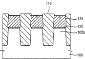
Figure 12 is the control grid layer that forms on the floating boom of explanation among Figure 11 and the profile of second dielectric layer.
With reference to Figure 12, in order to increase the coupling ratio of semiconductor device such as flash memory, can be etched in the top of field insulation patterns 116 outstanding on the surface of Semiconductor substrate 100 by for example anisotropic etch process or isotropic etching technology, partly to expose the sidewall of polysilicon graphics 134.In order to reduce or to prevent that first dielectric layer 120 etchant that uses in the insulation patterns 116 that is etched from damaging, and should not need to expose first dielectric layer 120 in the etching process of insulation patterns 116 on the scene.Can control etching technics according to etch period therebetween.For example, can use the etchant that comprises diluent hydrofluoric acid solution to remove the top of an insulation patterns 116.
Can form second dielectric layer 136 on insulation patterns 116 on the scene and the polysilicon graphics 134.The example of second dielectric layer 136 can comprise compound medium layer with oxide/nitride/oxide (ONO) and/or the dielectric layer with high-k.Compound medium layer can form by LPCVD technology.The example that is used to form the oxide of the dielectric layer with high-k comprises Y
2O
3, HfO
2, ZrO
2, Nb
2O
5, BaTiO
3And SrTiO
3These oxides can be used singly or in combination.In addition, the dielectric layer with high-k can form by atomic layer deposition (ALD) technology or CVD technology.Second dielectric layer 136, polysilicon graphics 134 and first dielectric layer 120 can be by compositions continuously, to form floating boom.
On second dielectric layer 136, can form control grid layer 142.Control grid layer 142 can comprise first conductive layer 138, second conductive layer 140, first conductive layer 138 comprises the polysilicon of doping, second conductive layer 140 comprises metal silicide, for example, and tungsten silicide (WSix), titanium silicide (TiSix), cobalt silicide (CoSix) and/or tantalum silicide (TaSix).
Optionally, in the both sides of grid structure, impurity can be injected among the active area 100b of Semiconductor substrate 100, to form the source/drain regions (not shown), finishes semiconductor device thus, for example flash memory.
In being no more than the semiconductor device of active area of 90nm width, manufacturing can easily adopt the method for present embodiment.In addition, the semiconductor device that has an active area that surpasses about 90nm width in manufacturing can adopt the method for present embodiment.
Figure 13 to 17 is profiles that the method for making semiconductor device according to another embodiment of the present invention is described.
In the present embodiment, can carry out and the process identical as mentioned above,, extend upward in the first party of crossing over Semiconductor substrate 200 to produce the field insulation patterns 210 of the active area 202 that can limit Semiconductor substrate 200 according to Fig. 1 to 5.As shown in figure 13, an insulation patterns 210 can have the bottom that is positioned at Semiconductor substrate 200, and the top of giving prominence on Semiconductor substrate 200.
Can with and Fig. 6 in first dielectric layer 120 method identical with first polysilicon layer 122, formation first dielectric layer 212 and first polysilicon layer on Semiconductor substrate 200.Therefore, as shown in figure 13, can be by the first polysilicon layer (not shown) that forms on the smooth insulation patterns 210 on the scene of chemico-mechanical polishing (CMP) technology and first dielectric layer 212, to form by the first preliminary polysilicon figure 214 of an insulation patterns 210 and dielectric layer 212 qualifications.On the active area 202 of Semiconductor substrate 200, can form first dielectric layer, 212, the first dielectric layers 212 and can comprise silica or the advanced low-k materials material of low-k (or have).
In forming first polysilicon layer, can produce the space 216 in the top of the first preliminary polysilicon figure 214.
Figure 14 is the profile of the second preliminary polysilicon figure that forms on first dielectric layer of explanation among Figure 13.Figure 15 is the profile of the 3rd preliminary polysilicon figure that forms on first dielectric layer of explanation among Figure 13.
Refer to figs. 14 and 15, the surface portion of the first preliminary polysilicon figure 214 can be removed, and exposes the second preliminary polysilicon figure 218 of space 216a with formation.The surface portion of the second preliminary polysilicon figure 218 is removed, to form the 3rd preliminary polysilicon figure 222 and recess 220.
In exemplary embodiments, use SC-1 solution and/or NSC-1 solution sequentially etching second preliminary polysilicon figure 218 and the 3rd preliminary polysilicon figure 222.The space 216a that exposes by expansion forms recess 220.Recess 220 can be formed on corresponding to the position of exposing space 216a.The space 216a that exposes can have about 50 to about
 Width, and
 recess 220 can have about 100 to approximately
 Mean breadth.
In the etching technics that forms recess 220, pass through the hydrogen peroxide (H in SC-1 solution and/or the NSC-1 solution
2O
2) and polysilicon between the silicon oxide layer (not shown) that forms of reaction can be removed.For example, can use the hydrofluoric acid of dilution to remove silicon oxide layer.
Figure 16 is the profile of second polysilicon layer that forms on the 3rd preliminary polysilicon figure of explanation in Figure 15.Figure 17 is the profile of the polysilicon graphics that forms on the 3rd preliminary polysilicon figure of explanation among Figure 15.
Referring to figs. 16 and 17, on the 3rd preliminary polysilicon figure 222, form second polysilicon layer 224, to fill recess 220.Second polysilicon layer 224 can have 0.5 times thickness of the mean breadth that is no less than about recess 130.Second polysilicon layer 224 for example, can have about 50 to about
 Thickness.
Optionally, second polysilicon layer 224 and the 3rd preliminary figure 222 can partly and/or sequentially be removed, to form polysilicon graphics 226.
After forming polysilicon graphics 226, can use diluent hydrofluoric acid solution partly to remove an insulation patterns 210, partly to expose the sidewall of polysilicon graphics 226.On polysilicon graphics 226, sequentially form the second dielectric layer (not shown) and control grid layer (not shown).Control grid layer can be patterned, with the upwardly extending control gate in the side that is formed on the bearing of trend that is substantially perpendicular to polysilicon graphics 226.Second dielectric layer, polysilicon graphics 226 and first dielectric layer 212 can be by compositions continuously, to expose active area of semiconductor substrate 202.On the active area 202 that exposes, can form the source/drain regions (not shown).Impurity can be injected in the active area 202 that exposes, to form source/drain regions.
Said elements and the step identical with source/drain regions have been omitted at this with the production control grid.
Figure 18 and 22 is profiles that explanation another exemplary embodiment according to the present invention is made the method for semiconductor device.
Figure 18 and 19 is the first preliminary polysilicon figure that forms on active area of semiconductor substrate of explanation and the profile of first dielectric layer.
At this embodiment, can carry out with top according to the described identical process of Fig. 1 to 5, be formed on field insulation patterns 310 on the Semiconductor substrate 300 with generation.Field insulation patterns 310 can extend upward in the first party of crossing over Semiconductor substrate 300.Can buried portion another arena insulation patterns 310 in Semiconductor substrate 300.The active area 302 of Semiconductor substrate 300 can be limited by field insulation patterns 310.
Can with and Fig. 6 in first dielectric layer 120 method identical with first polysilicon layer 122, formation first dielectric layer 312 and first polysilicon layer on Semiconductor substrate 300.On Semiconductor substrate 300, can form first dielectric layer 312, for example silicon oxide layer.On first dielectric layer 312 and an insulation patterns 310, can form the first polysilicon layer (not shown).First polysilicon layer can be filled fully by the space of field insulation patterns 310 and 312 qualifications of first dielectric layer.
Can carry out chemico-mechanical polishing (CMP) technology, be exposed, on first dielectric layer 312, form the first preliminary polysilicon figure 314 thus until the upper surface of field insulation patterns 310.Simultaneously, expose space 316 in first polysilicon layer by CMP technology.
Omitted as process at this referring to figs. 1 to the first preliminary polysilicon figure 314 of the formation shown in 7.
After the CMP operation, can use diluent hydrofluoric acid solution partly to remove the top of an insulation patterns 310, partly to expose the sidewall of the first preliminary polysilicon figure 314.
Figure 20 is the profile of the second preliminary polysilicon figure that forms on first dielectric layer of explanation among Figure 18.
With reference to Figure 20, can enlarge the space 316 of exposing with the etchant of SC-1 solution and/or NSC-1 solution, to form the second preliminary polysilicon figure 320 and recess 318.Recess 318 can have " U " tee section, and can have about 100 to about
 Mean breadth.
Can remove by the wet-etching technology that uses diluent hydrofluoric acid solution, in the etching first preliminary polysilicon figure 314, by hydrogen peroxide (H
2O
2) and the first preliminary polysilicon figure 314 between be reflected on the second preliminary polysilicon figure 320 byproduct layer that forms, as silicon oxide layer.
Optionally, when under the upper surface of the first preliminary polysilicon figure 314, arranging the space, use time that SC-1 solution and/or NSC-1 solution etching need can Be Controlled, expose space 316 with upper surface by the first preliminary polysilicon figure 314.The space 316 of exposing can be extended, to form recess 318.
Figure 21 is the profile of second polysilicon layer that forms on the second preliminary polysilicon figure of explanation in Figure 20.
With reference to Figure 21, on the upper surface of the second preliminary polysilicon figure 320 and an insulation patterns 310 and sidewall, can form second polysilicon layer 322.
As shown in figure 21, on the second preliminary polysilicon figure 320, can form second polysilicon layer 322, to fill space 316.Second polysilicon layer 322 can have 0.5 times thickness of the mean breadth that is no less than about recess 318.For example, second polysilicon layer 322 can have about 50 to about
Thickness.
Figure 22 is the profile of second polysilicon graphics that forms in second dielectric layer of explanation among Figure 18.
With reference to Figure 22, the part of second polysilicon layer 322 and the second preliminary polysilicon figure 320 can partly be removed, to form polysilicon graphics 324.Can form the etching technics of polysilicon graphics 324 according to etch period control.In the exemplary embodiment, the thickness of hope can be no less than the thickness of second polysilicon layer 322.Therefore, part second polysilicon layer 322 on the insulation patterns 310 can fully be removed.
On polysilicon graphics 324, can sequentially form the second dielectric layer (not shown) and control grid layer (not shown).Control grid layer can be patterned, to be formed on perpendicular to the upwardly extending control gate of the second party of first direction.Second dielectric layer, polysilicon graphics 324 and first dielectric layer 312 can be by compositions continuously, with the active area 302 that exposes Semiconductor substrate 300.On the both sides of the active area 302 that exposes, can form the source/drain regions (not shown).
As mentioned above, comprise in the semiconductor device with the active area that is no more than about 90nm width, can adopt the method for making semiconductor device according to exemplary embodiments in manufacturing.
According to exemplary embodiments of the present invention, the space that produces in the manufacture process of the semiconductor device with floating boom can be removed.Therefore, second dielectric layer on the floating boom can have improved breakdown voltage performance and/or leakage current performance.Simultaneously, can increase the coupling ratio of capacitor.
In addition, comprise the method that can adopt formation exemplary embodiments of the present invention in the semiconductor device with the active area that is no more than about 90nm width effectively in manufacturing.
Above be the explanation of exemplary embodiments of the present invention and do not allow to think its restriction.Although described exemplary embodiments of the present invention, the those skilled in the art will easily understand under the condition that breaks away from novel teachings of the present invention and advantage indistinctively, and many improvement of exemplary embodiments are possible.Thus, all this improvement are defined as being included in the scope of the present invention of claim qualification.Therefore, be to be understood that above to be explanation of the present invention and not allow to think to be limited to disclosed specific embodiment, and the improvement of open exemplary embodiments and other embodiment is defined as being included in the scope of additional claim.
Claims (34)
1. method of making semiconductor device comprises:
Form insulation patterns on substrate, insulation patterns has at least one opening that exposes substrate surface;
Form first polysilicon layer on substrate, so that the first polysilicon layer filling opening, first polysilicon layer is included in space wherein;
Remove the top of first polysilicon layer, so that recess is expanded in the space to, and recess is exposed; And
On substrate, form second polysilicon layer, so that second polysilicon layer is filled recess.
According to the process of claim 1 wherein in forming recess remove step with the width in space from 50 scopes to the expanded range to 100 of 100 dusts to 300 dusts.
3. according to the method for claim 2, wherein form second polysilicon layer that the second polysilicon layer step forms the 0.5 times of thickness that is no less than recess width.
4. according to the process of claim 1 wherein that removing step enlarges the space to form recess by wet etching.
5. according to the method for claim 4, wherein wet-etching technology uses the mixture of ammonium hydroxide, hydrogen peroxide and water.
6. according to the process of claim 1 wherein that this is removed step and comprises:
Smooth first polysilicon layer is to expose the space; And
Enlarge the space, to form recess.
7. according to the method for claim 6, wherein carry out planarization step by chemico-mechanical polishing.
8. according to the method for claim 6, wherein expansion step enlarges the space to form recess by wet etching.
9. according to the method for claim 6, before forming the first polysilicon layer step, also comprise:
On the exposed portions serve of substrate, form first medium.
10. according to the method for claim 9, after planarization step and before expansion step, also comprise:
Remove the top of insulation patterns, to expose the sidewall of first polysilicon layer.
11. according to the method for claim 10, the top step of wherein removing insulation patterns does not make the height of insulation patterns reduce to be lower than the upper surface of substrate.
12. the method according to claim 10 also comprises:
Remove the top of second polysilicon layer.
13. according to the method for claim 12, wherein remove top step etching second polysilicon layer of second polysilicon layer, so that part second polysilicon layer not in recess is fully removed.
14. the method according to claim 12 also comprises:
Behind the top of removing second polysilicon layer, on substrate, form second dielectric layer.
15. the method according to claim 14 also comprises:
On second dielectric layer, form control grid layer.
16. according to the method for claim 15, wherein form first polysilicon layer, and form second medium and control grid layer along second direction perpendicular to first direction along first direction.
17., wherein form the control grid layer that the control grid layer step forms first and second conductive layers according to the method for claim 15.
18. according to the process of claim 1 wherein remove step remove first polysilicon layer to small part top, and enlarge the space to form recess by wet etching.
19. according to the method for claim 18, wherein wet etching remove first polysilicon layer to small part top, so that the space is exposed.
20., wherein before wet etching first polysilicon layer, remove smooth first polysilicon layer of step according to the method for claim 18.
21., before forming the first polysilicon layer step, also comprise according to the method for claim 1:
On the exposed portions serve of substrate, form first medium.
22. the method according to claim 21 also comprises:
Remove the top of second polysilicon layer.
23. according to the method for claim 22, wherein remove top step etching second polysilicon layer of second polysilicon layer, so that part second polysilicon layer not in recess is fully removed.
24., after removing the top step of second polysilicon layer, also comprise according to the method for claim 22:
Remove the top of insulation patterns, to expose the sidewall of first polysilicon layer.
25. according to the method for claim 24, the top step of wherein removing insulation patterns does not make the height of insulation patterns reduce to be lower than the upper surface of Semiconductor substrate.
26. the method according to claim 24 also comprises:
Behind the top of removing second polysilicon layer, on substrate, form second dielectric layer.
27. the method according to claim 26 also comprises:
On second dielectric layer, form control grid layer.
28. according to the method for claim 27, wherein form first polysilicon layer, and form second medium and control grid layer along second direction perpendicular to first direction along first direction.
29., wherein form the control grid layer that the control grid layer step forms first and second conductive layers according to the method for claim 27.
30. a method of making semiconductor device comprises:
Formation has the figure of opening, and opening exposes the surface of substrate;
At this figure with expose and form first polysilicon layer on the surface of substrate, with filling opening;
Smooth first polysilicon layer is exposed until the upper surface of figure, to form first polysilicon graphics in opening;
Form recess selectively by upper surface and remove space in first polysilicon graphics at first polysilicon graphics;
On this figure, form second polysilicon layer; And
Partly remove second polysilicon layer, to form second polysilicon graphics.
31. according to the method for claim 30, wherein by using ammonium hydroxide (NH
4OH), hydrogen peroxide (H
2O
2) and water (H
2The wet-etching technology of mixture O) is removed the space.
32., also comprise and removing by hydrogen peroxide (H according to the method for claim 31
2O
2) and first polysilicon graphics between the oxide that forms of reaction.
33. according to the method for claim 30, wherein form recess by enlarging the space, expose by the upper surface of smooth first polysilicon layer from first polysilicon graphics in this space.
34., wherein form recess and comprise according to the method for claim 30:
Expose the space in first polysilicon graphics; And
Enlarge the space of exposing, to form recess.
Applications Claiming Priority (2)
| Application Number | Priority Date | Filing Date | Title |
|---|---|---|---|
| KR1020040085629 | 2004-10-26 | ||
| KR1020040085629A KR100552588B1 (en) | 2004-10-26 | 2004-10-26 | Method of manufacturing a semiconductor device |
Publications (2)
| Publication Number | Publication Date |
|---|---|
| CN1779916A CN1779916A (en) | 2006-05-31 |
| CN100576450C true CN100576450C (en) | 2009-12-30 |
Family
ID=36206703
Family Applications (1)
| Application Number | Title | Priority Date | Filing Date |
|---|---|---|---|
| CN200510116124A Expired - Fee Related CN100576450C (en) | 2004-10-26 | 2005-10-26 | Make the method for semiconductor device |
Country Status (4)
| Country | Link |
|---|---|
| US (1) | US7582559B2 (en) |
| JP (1) | JP5068442B2 (en) |
| KR (1) | KR100552588B1 (en) |
| CN (1) | CN100576450C (en) |
Families Citing this family (16)
| Publication number | Priority date | Publication date | Assignee | Title |
|---|---|---|---|---|
| KR100763228B1 (en) * | 2006-03-20 | 2007-10-04 | 삼성전자주식회사 | Method for fabricating nonvolatile semiconductor memory device |
| US7998809B2 (en) * | 2006-05-15 | 2011-08-16 | Micron Technology, Inc. | Method for forming a floating gate using chemical mechanical planarization |
| TWI316746B (en) | 2006-10-03 | 2009-11-01 | Macronix Int Co Ltd | Non-volatile memory and method of manufacturing the same |
| KR100790999B1 (en) * | 2006-10-17 | 2008-01-03 | 삼성전자주식회사 | Method of forming fine patterns of semiconductor device using double patterning process |
| CN101770954A (en) * | 2008-12-29 | 2010-07-07 | 中芯国际集成电路制造(上海)有限公司 | Forming method of flash memory |
| KR101652879B1 (en) | 2010-05-25 | 2016-09-02 | 삼성전자주식회사 | Non-volatile memory device and method of manufacturing the same |
| KR20120026313A (en) * | 2010-09-09 | 2012-03-19 | 삼성전자주식회사 | Non-volatile memory device and method of fabricating the same |
| US8722320B2 (en) * | 2011-07-27 | 2014-05-13 | Micron Technology, Inc. | Lithography method and device |
| US8846452B2 (en) * | 2012-08-21 | 2014-09-30 | Infineon Technologies Ag | Semiconductor device package and methods of packaging thereof |
| US20140273467A1 (en) * | 2013-03-14 | 2014-09-18 | Intermolecular Inc. | Polycrystalline-silicon etch with low-peroxide apm |
| CN104716084B (en) * | 2013-12-12 | 2017-10-27 | 华邦电子股份有限公司 | The manufacture method of semiconductor element |
| CN105336591B (en) * | 2014-07-01 | 2018-10-23 | 中芯国际集成电路制造(上海)有限公司 | The production method of floating boom |
| JP2017152531A (en) * | 2016-02-24 | 2017-08-31 | 東京エレクトロン株式会社 | Substrate processing method |
| US10559571B2 (en) | 2017-04-13 | 2020-02-11 | Samsung Electronics Co., Ltd. | Methods of fabricating semiconductor memory devices |
| CN110931432A (en) * | 2018-09-19 | 2020-03-27 | 长鑫存储技术有限公司 | Semiconductor device and method for manufacturing the same |
| CN109616409B (en) * | 2018-12-04 | 2021-03-23 | 武汉新芯集成电路制造有限公司 | Polycrystalline silicon deposition method, flash memory and manufacturing method thereof |
Family Cites Families (9)
| Publication number | Priority date | Publication date | Assignee | Title |
|---|---|---|---|---|
| JP3362970B2 (en) * | 1994-08-19 | 2003-01-07 | 株式会社東芝 | Nonvolatile semiconductor memory device and method of manufacturing the same |
| JP3264326B2 (en) | 1999-03-17 | 2002-03-11 | 日本電気株式会社 | Method for manufacturing semiconductor device |
| KR100356821B1 (en) | 2000-02-28 | 2002-10-18 | 주식회사 하이닉스반도체 | Non-volatile semiconductor memory device and fabricating method thereof |
| KR100415518B1 (en) * | 2000-06-30 | 2004-01-31 | 주식회사 하이닉스반도체 | Method for manufacturing a flash memory cell |
| KR100400037B1 (en) * | 2001-02-22 | 2003-09-29 | 삼성전자주식회사 | Semiconductor device with contact plug and method for manufacturing the same |
| US6908862B2 (en) * | 2002-05-03 | 2005-06-21 | Applied Materials, Inc. | HDP-CVD dep/etch/dep process for improved deposition into high aspect ratio features |
| KR100590396B1 (en) | 2002-07-04 | 2006-06-15 | 주식회사 하이닉스반도체 | Method of manufacturing a flash memory cell |
| KR100482366B1 (en) * | 2002-07-15 | 2005-04-13 | 삼성전자주식회사 | method for fabricating storage capacitor in semiconductor memory device |
| KR100539275B1 (en) * | 2004-07-12 | 2005-12-27 | 삼성전자주식회사 | Method of manufacturing a semiconductor device |
-
2004
- 2004-10-26 KR KR1020040085629A patent/KR100552588B1/en active IP Right Grant
-
2005
- 2005-10-14 US US11/249,515 patent/US7582559B2/en not_active Expired - Fee Related
- 2005-10-20 JP JP2005305543A patent/JP5068442B2/en not_active Expired - Fee Related
- 2005-10-26 CN CN200510116124A patent/CN100576450C/en not_active Expired - Fee Related
Also Published As
| Publication number | Publication date |
|---|---|
| CN1779916A (en) | 2006-05-31 |
| US7582559B2 (en) | 2009-09-01 |
| KR100552588B1 (en) | 2006-02-15 |
| US20060088987A1 (en) | 2006-04-27 |
| JP5068442B2 (en) | 2012-11-07 |
| JP2006128673A (en) | 2006-05-18 |
Similar Documents
| Publication | Publication Date | Title |
|---|---|---|
| CN100576450C (en) | Make the method for semiconductor device | |
| US7410869B2 (en) | Method of manufacturing a semiconductor device | |
| US7459364B2 (en) | Methods of forming self-aligned floating gates using multi-etching | |
| KR100475081B1 (en) | SONOS type EEPROM and method for fabricating the same | |
| KR100436406B1 (en) | Semiconductor memory device with floating-gate and manufacturing method thereof | |
| US7498233B2 (en) | Method of forming an insulation layer structure having a concave surface and method of manufacturing a memory device using the same | |
| US6570215B2 (en) | Nonvolatile memories with floating gate spacers, and methods of fabrication | |
| US7186607B2 (en) | Charge-trapping memory device and method for production | |
| US7902059B2 (en) | Methods of forming void-free layers in openings of semiconductor substrates | |
| US20080197403A1 (en) | Semiconductor device | |
| KR100313695B1 (en) | A method of making semiconductor apparatus | |
| KR20030069800A (en) | Single sided buried strap | |
| CN101022126B (en) | Semiconductor device and related fabrication method | |
| KR20030001230A (en) | Semiconductor device and method of manufacturing the same | |
| US6537880B1 (en) | Method of fabricating a high density NAND stacked gate flash memory device having narrow pitch isolation and large capacitance between control and floating gates | |
| JP2005530357A (en) | Floating gate extended with conductive spacer | |
| KR100589058B1 (en) | Non-volatile memory device and method for forming the same | |
| US6962852B2 (en) | Nonvolatile memories and methods of fabrication | |
| CN100446257C (en) | Dynamic random access memory and mfg. method thereof | |
| KR20060012695A (en) | Method of manufacturing a semiconductor device | |
| KR100652383B1 (en) | Method of manufacturing a semiconductor device | |
| KR20070064763A (en) | Method of forming a semiconductor device | |
| KR20060025262A (en) | Method of manufacturing a semiconductor device | |
| KR20060112772A (en) | Method of manufacturing a semiconductor device | |
| US20100124807A1 (en) | Method of manufacturing semiconductor device having step gates |
Legal Events
| Date | Code | Title | Description |
|---|---|---|---|
| C06 | Publication | ||
| PB01 | Publication | ||
| C10 | Entry into substantive examination | ||
| SE01 | Entry into force of request for substantive examination | ||
| C14 | Grant of patent or utility model | ||
| GR01 | Patent grant | ||
| CF01 | Termination of patent right due to non-payment of annual fee |
Granted publication date: 20091230 Termination date: 20211026 |
|
| CF01 | Termination of patent right due to non-payment of annual fee |