CN100565807C - In charge erasure optical exposure instrument, remove the method for the gas of inhaling wavelength - Google Patents
In charge erasure optical exposure instrument, remove the method for the gas of inhaling wavelength Download PDFInfo
- Publication number
- CN100565807C CN100565807C CNB2007101287719A CN200710128771A CN100565807C CN 100565807 C CN100565807 C CN 100565807C CN B2007101287719 A CNB2007101287719 A CN B2007101287719A CN 200710128771 A CN200710128771 A CN 200710128771A CN 100565807 C CN100565807 C CN 100565807C
- Authority
- CN
- China
- Prior art keywords
- wavelength
- electric charge
- integrated circuit
- gas
- wafer
- Prior art date
- Legal status (The legal status is an assumption and is not a legal conclusion. Google has not performed a legal analysis and makes no representation as to the accuracy of the status listed.)
- Expired - Fee Related
Links
- 238000000034 method Methods 0.000 title claims abstract description 52
- 230000003287 optical effect Effects 0.000 title claims abstract description 13
- 230000008569 process Effects 0.000 claims abstract description 42
- 230000005855 radiation Effects 0.000 claims abstract description 39
- 239000007789 gas Substances 0.000 claims description 12
- 238000010521 absorption reaction Methods 0.000 claims description 7
- 239000011261 inert gas Substances 0.000 claims description 7
- XKRFYHLGVUSROY-UHFFFAOYSA-N Argon Chemical compound [Ar] XKRFYHLGVUSROY-UHFFFAOYSA-N 0.000 claims description 4
- IJGRMHOSHXDMSA-UHFFFAOYSA-N Atomic nitrogen Chemical compound N#N IJGRMHOSHXDMSA-UHFFFAOYSA-N 0.000 claims description 4
- 239000000203 mixture Substances 0.000 claims description 3
- 229910052786 argon Inorganic materials 0.000 claims description 2
- 239000001307 helium Substances 0.000 claims description 2
- 229910052734 helium Inorganic materials 0.000 claims description 2
- SWQJXJOGLNCZEY-UHFFFAOYSA-N helium atom Chemical compound [He] SWQJXJOGLNCZEY-UHFFFAOYSA-N 0.000 claims description 2
- 229910052757 nitrogen Inorganic materials 0.000 claims description 2
- 238000009825 accumulation Methods 0.000 abstract description 34
- 230000035508 accumulation Effects 0.000 description 32
- 235000012431 wafers Nutrition 0.000 description 27
- 238000012545 processing Methods 0.000 description 12
- 230000000694 effects Effects 0.000 description 9
- 238000004519 manufacturing process Methods 0.000 description 9
- 239000000463 material Substances 0.000 description 8
- 238000005516 engineering process Methods 0.000 description 7
- 229910052751 metal Inorganic materials 0.000 description 7
- 239000002184 metal Substances 0.000 description 7
- 238000001228 spectrum Methods 0.000 description 6
- 239000000523 sample Substances 0.000 description 5
- 238000013461 design Methods 0.000 description 4
- 239000010453 quartz Substances 0.000 description 4
- VYPSYNLAJGMNEJ-UHFFFAOYSA-N silicon dioxide Inorganic materials O=[Si]=O VYPSYNLAJGMNEJ-UHFFFAOYSA-N 0.000 description 4
- CBENFWSGALASAD-UHFFFAOYSA-N Ozone Chemical compound [O-][O+]=O CBENFWSGALASAD-UHFFFAOYSA-N 0.000 description 3
- 238000004140 cleaning Methods 0.000 description 3
- 238000005530 etching Methods 0.000 description 3
- 230000006870 function Effects 0.000 description 3
- QSHDDOUJBYECFT-UHFFFAOYSA-N mercury Chemical compound [Hg] QSHDDOUJBYECFT-UHFFFAOYSA-N 0.000 description 3
- 230000003595 spectral effect Effects 0.000 description 3
- 238000003860 storage Methods 0.000 description 3
- 238000000137 annealing Methods 0.000 description 2
- QVGXLLKOCUKJST-UHFFFAOYSA-N atomic oxygen Chemical compound [O] QVGXLLKOCUKJST-UHFFFAOYSA-N 0.000 description 2
- 230000004888 barrier function Effects 0.000 description 2
- 230000008901 benefit Effects 0.000 description 2
- 230000008859 change Effects 0.000 description 2
- 239000011248 coating agent Substances 0.000 description 2
- 238000000576 coating method Methods 0.000 description 2
- 238000011109 contamination Methods 0.000 description 2
- 238000001816 cooling Methods 0.000 description 2
- 230000005611 electricity Effects 0.000 description 2
- 230000004927 fusion Effects 0.000 description 2
- 238000010438 heat treatment Methods 0.000 description 2
- 239000007788 liquid Substances 0.000 description 2
- 239000001301 oxygen Substances 0.000 description 2
- 229910052760 oxygen Inorganic materials 0.000 description 2
- 239000000758 substrate Substances 0.000 description 2
- 208000013935 Electric injury Diseases 0.000 description 1
- 239000011149 active material Substances 0.000 description 1
- 238000004380 ashing Methods 0.000 description 1
- 125000004429 atom Chemical group 0.000 description 1
- 230000005540 biological transmission Effects 0.000 description 1
- 238000006243 chemical reaction Methods 0.000 description 1
- 150000001875 compounds Chemical class 0.000 description 1
- 230000006378 damage Effects 0.000 description 1
- 230000002950 deficient Effects 0.000 description 1
- 230000001066 destructive effect Effects 0.000 description 1
- 238000011161 development Methods 0.000 description 1
- 230000018109 developmental process Effects 0.000 description 1
- 239000002784 hot electron Substances 0.000 description 1
- 238000005286 illumination Methods 0.000 description 1
- 150000002500 ions Chemical class 0.000 description 1
- 229910052753 mercury Inorganic materials 0.000 description 1
- 230000000149 penetrating effect Effects 0.000 description 1
- 229910021420 polycrystalline silicon Inorganic materials 0.000 description 1
- 229920005591 polysilicon Polymers 0.000 description 1
- 150000003254 radicals Chemical class 0.000 description 1
- 230000008672 reprogramming Effects 0.000 description 1
- 230000027756 respiratory electron transport chain Effects 0.000 description 1
- 238000006748 scratching Methods 0.000 description 1
- 230000002393 scratching effect Effects 0.000 description 1
- 230000011218 segmentation Effects 0.000 description 1
- 239000002023 wood Substances 0.000 description 1
Images


Classifications
-
- H—ELECTRICITY
- H01—ELECTRIC ELEMENTS
- H01L—SEMICONDUCTOR DEVICES NOT COVERED BY CLASS H10
- H01L29/00—Semiconductor devices adapted for rectifying, amplifying, oscillating or switching, or capacitors or resistors with at least one potential-jump barrier or surface barrier, e.g. PN junction depletion layer or carrier concentration layer; Details of semiconductor bodies or of electrodes thereof ; Multistep manufacturing processes therefor
- H01L29/66—Types of semiconductor device ; Multistep manufacturing processes therefor
- H01L29/66007—Multistep manufacturing processes
- H01L29/66075—Multistep manufacturing processes of devices having semiconductor bodies comprising group 14 or group 13/15 materials
- H01L29/66227—Multistep manufacturing processes of devices having semiconductor bodies comprising group 14 or group 13/15 materials the devices being controllable only by the electric current supplied or the electric potential applied, to an electrode which does not carry the current to be rectified, amplified or switched, e.g. three-terminal devices
- H01L29/66409—Unipolar field-effect transistors
- H01L29/66477—Unipolar field-effect transistors with an insulated gate, i.e. MISFET
- H01L29/66825—Unipolar field-effect transistors with an insulated gate, i.e. MISFET with a floating gate
-
- H—ELECTRICITY
- H01—ELECTRIC ELEMENTS
- H01L—SEMICONDUCTOR DEVICES NOT COVERED BY CLASS H10
- H01L21/00—Processes or apparatus adapted for the manufacture or treatment of semiconductor or solid state devices or of parts thereof
- H01L21/02—Manufacture or treatment of semiconductor devices or of parts thereof
- H01L21/04—Manufacture or treatment of semiconductor devices or of parts thereof the devices having at least one potential-jump barrier or surface barrier, e.g. PN junction, depletion layer or carrier concentration layer
- H01L21/18—Manufacture or treatment of semiconductor devices or of parts thereof the devices having at least one potential-jump barrier or surface barrier, e.g. PN junction, depletion layer or carrier concentration layer the devices having semiconductor bodies comprising elements of Group IV of the Periodic System or AIIIBV compounds with or without impurities, e.g. doping materials
- H01L21/26—Bombardment with radiation
- H01L21/263—Bombardment with radiation with high-energy radiation
- H01L21/268—Bombardment with radiation with high-energy radiation using electromagnetic radiation, e.g. laser radiation
-
- H—ELECTRICITY
- H01—ELECTRIC ELEMENTS
- H01L—SEMICONDUCTOR DEVICES NOT COVERED BY CLASS H10
- H01L21/00—Processes or apparatus adapted for the manufacture or treatment of semiconductor or solid state devices or of parts thereof
- H01L21/02—Manufacture or treatment of semiconductor devices or of parts thereof
- H01L21/04—Manufacture or treatment of semiconductor devices or of parts thereof the devices having at least one potential-jump barrier or surface barrier, e.g. PN junction, depletion layer or carrier concentration layer
- H01L21/18—Manufacture or treatment of semiconductor devices or of parts thereof the devices having at least one potential-jump barrier or surface barrier, e.g. PN junction, depletion layer or carrier concentration layer the devices having semiconductor bodies comprising elements of Group IV of the Periodic System or AIIIBV compounds with or without impurities, e.g. doping materials
- H01L21/28—Manufacture of electrodes on semiconductor bodies using processes or apparatus not provided for in groups H01L21/20 - H01L21/268
- H01L21/28008—Making conductor-insulator-semiconductor electrodes
- H01L21/28017—Making conductor-insulator-semiconductor electrodes the insulator being formed after the semiconductor body, the semiconductor being silicon
- H01L21/28158—Making the insulator
- H01L21/28167—Making the insulator on single crystalline silicon, e.g. using a liquid, i.e. chemical oxidation
- H01L21/28176—Making the insulator on single crystalline silicon, e.g. using a liquid, i.e. chemical oxidation with a treatment, e.g. annealing, after the formation of the definitive gate conductor
-
- H—ELECTRICITY
- H01—ELECTRIC ELEMENTS
- H01L—SEMICONDUCTOR DEVICES NOT COVERED BY CLASS H10
- H01L29/00—Semiconductor devices adapted for rectifying, amplifying, oscillating or switching, or capacitors or resistors with at least one potential-jump barrier or surface barrier, e.g. PN junction depletion layer or carrier concentration layer; Details of semiconductor bodies or of electrodes thereof ; Multistep manufacturing processes therefor
- H01L29/66—Types of semiconductor device ; Multistep manufacturing processes therefor
- H01L29/66007—Multistep manufacturing processes
- H01L29/66075—Multistep manufacturing processes of devices having semiconductor bodies comprising group 14 or group 13/15 materials
- H01L29/66227—Multistep manufacturing processes of devices having semiconductor bodies comprising group 14 or group 13/15 materials the devices being controllable only by the electric current supplied or the electric potential applied, to an electrode which does not carry the current to be rectified, amplified or switched, e.g. three-terminal devices
- H01L29/66409—Unipolar field-effect transistors
- H01L29/66477—Unipolar field-effect transistors with an insulated gate, i.e. MISFET
Abstract
A kind of be used for by the process that optical instrument reduces the electric charge accumulation of integrated circuit comprise with described integrated circuit or wherein part be exposed under the broadband radiation source.This process has reduced the electric charge accumulation that produces effectively in making integrated circuit.
Description
This case is the division of female case (applying date: 2002.12.02, application number: 02823776.5, denomination of invention: be used for wiping at the method and apparatus of making integrated circuit process charges accumulated).
Background of invention
Relate to the process and the equipment that are used to make integrated circuit on the disclosure file population, more specifically say, relate to the process and the equipment that are used for removing or reducing the electric charge accumulation that during the manufacturing integrated circuit (IC)-components, is produced by optical instrument.
At the industrial integrated circuit that has proposed or used multiple employing nonvolatile memory (NVM) array.Nonvolatile memory array is usually based on Floating-gate Technology.This technology refers to by oxide skin(coating) or dielectric layer electric charge is transferred to the floating boom of conduction, then in this floating boom place storage or remove electric charge.Adopting the example of the nonvolatile memory array device of Floating-gate Technology is EPROM (Erasable Programmable Read Only Memory) (" EPROM ") device, and this device can be read, wipes and write (promptly able to programme).EPROM generally uses floating gate fet, and this transistor has the bifurcation that depends on that electric charge exists or lacks on this floating boom.By being that electronics is stored in the floating boom with electric charge, thus with storage in nonvolatile memory device.
Can obtain multiple EPROM.In traditional and the most basic form, EPROM programmes by the method for electricity, and wipes by being exposed under the ultraviolet light.The EPROM of these types is commonly referred to as ultraviolet Erasable Programmable Read Only Memory EPROM (" UVEPROM ").Apply the positive potential UVEPROM that programmes to grid simultaneously by between UVEPROM transistor drain and source electrode, passing to high electric current.Positive potential on grid attracts from high energy (instant heating) electronics of the channel current of drain-to-source, electron transfer or inject floating boom and be captured at floating boom in this channel current.Be designed to wipe their electric charge by optical instrument based on the UVEPROM of this technology.In this method, when the needs reprogramming, can get off to remove charge stored by this device is exposed to ultraviolet light.
The example of UVEPROM shown in Figure 1.This device unification is designated as 10, and it comprises source region 12 and the drain region 14 that is formed on the n type substrate 16.Gate oxide film 18 is formed on the substrate surface on the raceway groove between source region 12 and the drain region 14.The floating gate electrode 20 that is made of p type polysilicon etc. typically is arranged on the gate oxide film 18.Because UVEPROM is designed to wipe their electric charge by optical instrument, so can remove any electric charge accumulation that produces under the ultraviolet light in manufacture process by these devices are exposed in manufacture process.
The EPROM of another kind of form is the programmable read only memory that can wipe by the electricity means, and this memory is also called and is " EEPROM " or " E2PROM ".Normally electrically programme and wipe EEPROM by means of known Fowler-Nordheim tunnel effect.During operation, these devices are not to be designed to wipe by optical instrument.Therefore, during making integrated circuit, may produce dangerous electric charge accumulation.
Also have the EPROM of another kind of form to be " flash EPROM ", it uses hot electron to programme, and uses Fowler-Nordheim tunnel effect phenomenon to wipe.Can wipe flash EPROM with " fast " or batch mode, wherein all unit in the array or partial array can use the Fowler-Nordheim tunnel effect to wipe simultaneously.Flash EPROM is so-called to be " flash cell " or " flush memory device ".Be similar to the EEPROM device, the electric charge accumulation that is produced during manufacturing flash EPROM device is not designed to wipe by optical instrument.As shown in FIG. 2, the EEPROM of exemplary or flash EPROM device generally include the additional conductive grid layer 22 that is arranged on the floating boom 20.
During making integrated circuit, well-knownly be on (if adaptable words) on the floating boom such as the EPROM device and/or other zones, can produce undesirable electric charge accumulation at this integrated circuit.If these electric charge accumulations are not removed or are neutralized, then these electric charge accumulations may cause high voltage and circuit is caused electric injury.Usually be easy to generate the electric charge accumulation in step in numerous treatment steps of making integrated circuit or the multistep.For example, accumulate all may producing electric charge during the annealing in process, during medal polish or the etching processing, after through hole and pad form step etc.Integrated circuit typically uses 3 to 5 layers of conductive metal layer, and these metal levels comprise that during manufacture about 5 are accumulated contributive treatment step to about 7 for electric charge.It is important wiping these electric charge accumulations when making device.
Current manufacture process is devoted to wipe the electric charge accumulation that produces during the integrated circuit making, and particularly wipes electric charge accumulation by using such as the integrated circuit of the nonvolatile memory device of EEPROM that mentions and flash memory in the above.Can use electric probe to provide and be connected, thereby realize wiping the electric charge accumulation so that apply needed voltage with the interim of circuit.Yet this method expends time in and is not practicable for large batch of production.Use the erasing time of electric probe to be typically greater than about 10 minutes clock time/each wafer, and may be greater than 1 hour/each wafer according to specific circuit design.
By being exposed to, this integrated circuit also can remove the electric charge accumulation under the narrow-band radiated source.The current process use mercury electrode lamp that is used to remove electric charge, this lamp produces the arrowband wave spectrum that wavelength is approximately 254nm.Mercury vapor lamp emission high-energy photon, heap is passed to the electronics of storage and the electric charge of other existence with energy thereby high-energy photon passes integrated circuit.These electronics of energizing overcome the energy barrier of previous restriction electronics and other electric charges, and are compound again between IC interior electronics and electron hole or positive charge.Also increased charge mobility on other zones of this integrated circuit in the exposure under the arrowband UV light.
In UVEPROM, to remove the electric charge accumulation by exposure under the narrow-band radiated source and be considered to usually effectively, this is because such device just is configured for during operation at first and wipes by optical instrument.The oxide skin(coating) or the dielectric layer that are arranged on the floating boom are transparent for the narrow-band radiated that the wavelength by the mercury vapor lamp emission is approximately 254nm.
Yet, the current processing procedure of using narrow-band light source is invalid for removing that electric charge in the other types integrated circuit (IC)-components accumulates, these devices are arranged in floating gate electrode (EEPROM for example such as comprising, the device of the conduction flash memory etc.) (for example metal) grid layer, perhaps other the device that is included in the multiple layer metal line on the floating-gate memory unit.As shown in Figure 2, the existence of conductive gate layer 22 has been played and has been stopped that incident radiation arrives the effect of following floating gate electrode 20, and this greatly reduces its efficiency of erasing.As a result, the time for exposure that need grow of current exposure tool (promptly according to specific I C design for each wafer needs approximately greater than 1 or 2 hours) reduce the electric charge accumulation.
Time for exposure is directly depended on the intensity (and other factors) of light source.The intensity of light source of employed current artificial light source is limited in (for example) average every square centimeter of about 30 milliwatt power (mW/cm in exposure tool
2), when lamp can reach about 60mW/cm when being new
2Yet employed narrow-band light source produces and comprises transmitting of discrete and narrow spectral line, has low total output intensity at every spectral line place.Although can change the wave spectrum output of prior art light source to a certain extent, the spectral line that obtains does not comprise very big power or the luminous intensity output that departs from former emission (about 254nm).
The current light source that is used to reduce the electric charge accumulation depends on the bulb technologies of using internal electrode.Be known that: the bulb intensity of use internal electrode can significantly reduce the useful life of bulb.The user usually needed intensity is reduced to (being compared to new bulb) 50% so that make the cost minimization of replacement before replacing these bulbs.As a result, bulb will cause the minimizing of output along with the time more and more worsens.The other problems that uses the prior art bulb to be produced comprises the long cooling time (reaching several hrs) of lamp, usually needs the long duration to make the bulb cooling so that replace bulb.Present high failure rate when in addition, the bulb of these types is lighted again after lamp is closed.Finally, many integrated circuits manufacturer does not typically close bulb in the non-use period of bulb, has influenced spendable working life greatly and has increased running cost for bulb like this.
Use the prior art light source except inefficent, and current exposure tool have big relatively footprint, the sizable floor space of these needs.In addition, this exposure tool typically requires the wafer manual load in instrument.This process be today work in-process only surplus need manually-operated step often.Manual operation has serious defective, may cause wafer fracture or damage to wafers (for example scratching), needs extra work investment, might cause wafer contamination and be difficult for being provided for the wafer track of automation.
Obviously need a kind of development that is used to reduce the electric charge accumulation during producing integrated circuit, particularly use the integrated circuit of nonvolatile memory device all the more so for those.Advanced design rule has further dwindled the figure that is used to make integrated circuit.Simultaneously, because also dwindled the minimum dimension in line and space, so added more metal line layer, metal wire wherein is more close.Final result is: the more difficult IC of the penetrating structure and the electric charge accumulation of wiping during manufacture process to be produced for the light of given narrowband wavelength.
Summary of the invention
Disclosed at this is process and the equipment that is used to remove producing the electric charge accumulation that is produced during the integrated circuit.In one embodiment, a kind ofly be used to remove the process of producing the electric charge accumulation during the integrated circuit and comprise that with this integrated circuit exposure in a kind of broadband radiation pattern next section period of intensity, described intensity and time can reduce charges accumulated during making integrated circuit effectively.
In another embodiment, a kind ofly be used for reducing the process of making the electric charge accumulation on floating gate electrode during the integrated circuit and comprise: this integrated circuit is placed on process chamber, and wherein this integrated circuit comprises floating gate electrode; And this integrated circuit was exposed in a kind of broadband radiation pattern next section period of intensity, and described intensity and time can reduce charges accumulated during making integrated circuit effectively.
Preferably, this broadband radiation pattern comprises at least a approximately less than the wavelength of 280nm, and FWHM is approximately greater than 10nm.
Feature described above and other features have been explained by following drawings and detailed description.
Description of drawings
With reference now to accompanying drawing,, wherein identical Reference numeral is represented identical part:
Fig. 1 illustrates the UVEPROM device of prior art;
Fig. 2 illustrates the EEPROM device of prior art;
Fig. 3 illustrate a kind of exemplary, be used to wipe the exposure tool of making the electric charge accumulation during the integrated circuit;
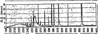
Fig. 4 graphic extension is used for the broadband wave spectrum output of a kind of electrodeless microwave-driven bulb of charge erasure; And
It is as the function that is exposed to the time for exposure of broadband radiation light source that Fig. 5 is illustrated in charge stored among the EEPROM.
Embodiment
A kind of process that is used to reduce the electric charge accumulation during making integrated circuit comprises exposes this integrated circuit in a kind of broadband radiation pattern next section period of intensity, and described intensity and time can reduce charges accumulated during making integrated circuit effectively.In a kind of embodiment preferred, during using nonvolatile memory device to make integrated circuit, use this process.Each stage in manufacture process can be used this process, and preferably, implement this process known during accumulating contributive treatment step for electric charge, such as after plasma ashing or etching processing, annealing in process, after through hole and pad form step etc.This process is preferably used after forming at least one conductive layer.
Though do not want to be subjected to the restriction of principle, be known that accumulation is contributive for electric charge such as some processing of mentioning in the above.For explanatory purposes, the wiring pattern of making the metal level of conduction generally includes the etching processing that plasma is reconciled, and wherein admixture of gas is exposed to energy source and separates this gas to produce plasma.This plasma contains active material, and these materials comprise energetic atom, free radical, ion, electronics and photon.These materials according to their concentration and energy level, may cause the electric charge accumulation in various degree at IC interior.
As used in this, term " broadband " radiation source refers to the radiation source with at least a wavelength band, this wavelength band has approximately greater than the half-peak breadth of 10nm, more preferably be this half-peak breadth approximately greater than 15nm, even more preferably be approximately greater than 20nm.Term half-peak breadth (FWHM) is defined herein as the width when a half that is reduced to peak value or peaked half leap wavelength curve.
Fig. 3 illustrates a kind of exposure tool 100 of exemplary, and it is suitable for reducing the electric charge accumulation during making integrated circuit.This exposure tool 100 generally comprises process chamber 112 and radiation source chamber 113.This process chamber 112 comprises chuck 114, arranges wafer 116 on chuck.Be to regulate chuck 114 or process chamber 112 alternatively to be provided at the thermal source (not shown) that is used for heated chip during the processing.A kind of example of optional heat is a kind of chuck of heating.Exposure tool 100 further comprise radiation source 118 and be arranged in radiation source 118 and chuck 114 between plate 120.Pipeline 122 is arranged making between itself and the process chamber 112 has liquid flow, thereby purifies this chamber 112 and regulate process chamber 112 pressure inside etc.Exposure tool 100 can comprise that also other feature is to be used for providing uniform exposure in wafer surface, described supplementary features are such as in the patent No. of authorizing people such as Matthews being architectural feature described in the United States Patent (USP) of No.4885047, and its integral body is incorporated herein by reference.To reduce needs for the uniform exposure of wafer surface,, thereby increase output with the accumulation of the electric charge in the All Ranges of guaranteeing to reduce wafer with nonvolatile memory array for overexposure.
In preferred embodiments, radiation source 118 uses the bulb of microwave-driven and the speculum of segmentation to come to provide full and uniform broadband radiation pattern to wafer.Suitable microwave-driven bulb is disclosed in people's such as Wood US Patent No 5541475.Had been found that the electrodeless bulb of a kind of well behaved exemplary microwave-driven, this bulb can obtain from the market, and trade mark is called the HL bulb, unit number 203662, and by being positioned at Rockville, the Axcelis Technologies company of Maryland produces.The wave spectrum that is produced by this broadband UV source shown in Figure 4 should be noted that to have a considerable amount of wave spectrum compositions less than 280nm.
This process comprises wafer 116 is loaded in the process chamber 112, and wafer 116 is exposed under the broadband radiation pattern by radiation source 118 emissions.Preferably, process chamber 112 is configured to realize the automatic processing of wafer 116, and without manual handle wafer 116.In preferred embodiments, remove air cleaning processing chamber 112, then wafer 116 is exposed under the broadband radiation pattern in process chamber 112 inside thereby this process comprises one or more inert gases of use.The suitable inert gas that is used for cleaning processing chamber 112 air includes, but are not limited to nitrogen, argon gas, helium, comprises the composition of at least a above-mentioned gas etc.
Air comprises about 21% oxygen.As everyone knows, the oxygen absorption wavelength is less than approximately radiation and the reaction of 200nm form products such as ozone.The generation of this ozone strengthens wavelength absorption conversely, and ozone begins radiation and the continuation absorption lower wavelength of absorbing wavelength up to 250nm.Finally reduced treatment effeciency.Cleaning processing chamber 112 and radiation source chamber 113 before wafer 116 is exposed to the broadband radiation pattern, thus reduce wavelength absorption and therefore improve treatment effeciency.
Integrated circuit is exposed to broadband radiation has many advantages.For example make constructive and destructive interference effect minimize.If the monofilm thickness of IC interior is the integral multiple of wavelength or half integer multiple then produces interference, and may cause having too much or very few illumination light to be passed and arrive lower layer.For the narrow-band radiated source of using single wavelength, this interference effect may seriously limit or reduce and be used to reduce the efficient that electric charge is accumulated.Be in contrast, interference effect from broadband radiation is minimized, this is that the influence that described a plurality of wavelength are not interfered is nondestructive or non-constructive for given film thickness promptly because it has used the broadband radiation pattern that comprises a plurality of wavelength.In addition, functional part for all size, the use of broadband radiation has been guaranteed: under the broadband radiation pattern, at least some wavelength in the various wavelength (are avoided shade) and are reflected near this functional part, and are penetrated into the layer heap bottom of typically arranging memory array.In addition, have been found that: can improve treatment effeciency greatly by wafer being exposed to short wavelength (less than 280nm).The long wavelength of shorter wavelength has higher photon energy, and therefore can apply more energy to electric charge, so just allows electric charge (for example electronics) more effectively to overcome the energy barrier that characterizes the electric charge accumulation.
Example 1
In this example, wafer is exposed under the broadband radiation pattern that is produced by FUSION PS3 exposure tool.This exposure tool is equipped with the HL bulb and is created in the wave spectrum figure shown in Fig. 4.FUSION PS3 exposure tool be obtainable on market, by being positioned at Rockville, the exposure tool that the Axcelis Technologies company of MD produces.Each wafer comprises a plurality of tube cores, and described a plurality of tube cores comprise nonvolatile memory (NVM or flash memory) structure, uses electric probe that this structure is programmed into charged state in advance.This non-volatile memory architecture comprises the grid of conduction, and the gate arrangement of conduction is on the floating gate electrode based on the 250nm design rule.The electrical power of supplying with magnetron in microwave circuit is 4500 watts (W), and microwave circuit is reduced to about 67% (approximately being 3000 watts for bulb promptly) to the efficiency of transmission of bulb.
Change the time for exposure for different wafer set, and the electric charge on the grid is depicted as the function of time.Under programming state, be normalized to " 1 " by the voltage that charge stored produced.According to the specification of manufacturer, for acceptable " wiping " state, acceptable boundary is pre the percentage of normalized programming state, and limits by horizontal dotted line on shown in Fig. 5.Fig. 5 illustrates that the state of charge of non-volatile memory architecture is the function that is exposed to the time for exposure of broadband radiation source.
This result clearlys show: for non-volatile memory architecture, with charge stored be reduced to acceptable level 1 minute with interior generation, this is showing sizable commercial advantage aspect minimizing efficient of output and electric charge accumulation.From the exposure that prolongs and with the electric charge accumulation maintain below the acceptable boundary effect as can be seen, this processing window is strong.That is to say that overexposure or over-erasure are not problems.The state that should be noted in the discussion above that charging can not be removed by optical instrument from floating boom fully.Reduce electric charge be accumulated to 0 need be such as the electrical input that uses electric probe etc.Yet this low voltage level charged state (upper limit as shown in FIG. 5) can be accepted as " erase status ", perhaps more specifically says " the UV-erase status " that be accepted as with respect to " electric erase status ".As discussing in front, it is very time-consuming and be not practicable aborning to use electric probe to reduce the electric charge accumulation.
Though embodiment explanation the present invention of reference example, it will be understood by those of skill in the art that and under the situation that does not deviate from the scope of the invention, can carry out various changes and equivalence replacement.For example, though explain and explanation be eeprom array, disclosedly be equally applicable to other use floating boom in the unit nonvolatile memory array, and even be applicable to the non-memory portion of non-memory integrated circuit or integrated circuit.In addition, can carry out many changes under the situation that does not deviate from base region of the present invention to adjust specific situation or material according to instruction of the present invention.Therefore, purpose of the present invention is not to limit disclosed particular as carrying out best pattern of the present invention, and the present invention will comprise that all fall into the embodiment in the accessory claim book scope.
What be required to protect is.
Claims (3)
1. one kind is used for removing the method for absorption 180nm to the gas of the wavelength of 200nm at charge erasure optical exposure instrument, and wherein this optical exposure instrument comprises the radiation source chamber of carrying out optical communication with process chamber, and this method comprises:
Use inert gas to purify this radiation source chamber, described inert gas is transparent for the wavelength of the GAS ABSORPTION that purifies in advance around the quilt; And
Use inert gas to purify this process chamber, described inert gas is transparent for 180nm to the wavelength of 200nm.
2. comprise nitrogen, helium, argon gas and the group that comprises the composition of at least a above-mentioned gas according to the process of claim 1 wherein that this inert gas is selected from.
3. according to the process of claim 1 wherein that the gas of absorbing wavelength comprises air.
Applications Claiming Priority (2)
| Application Number | Priority Date | Filing Date | Title |
|---|---|---|---|
| US10/000,772 US6605484B2 (en) | 2001-11-30 | 2001-11-30 | Process for optically erasing charge buildup during fabrication of an integrated circuit |
| US10/000772 | 2001-11-30 |
Related Parent Applications (1)
| Application Number | Title | Priority Date | Filing Date |
|---|---|---|---|
| CNB028237765A Division CN100336205C (en) | 2001-11-30 | 2002-12-02 | Process for optically erasing charge buildup during fabrication of an integrated circuit |
Publications (2)
| Publication Number | Publication Date |
|---|---|
| CN101145520A CN101145520A (en) | 2008-03-19 |
| CN100565807C true CN100565807C (en) | 2009-12-02 |
Family
ID=21692962
Family Applications (2)
| Application Number | Title | Priority Date | Filing Date |
|---|---|---|---|
| CNB2007101287719A Expired - Fee Related CN100565807C (en) | 2001-11-30 | 2002-12-02 | In charge erasure optical exposure instrument, remove the method for the gas of inhaling wavelength |
| CNB028237765A Expired - Fee Related CN100336205C (en) | 2001-11-30 | 2002-12-02 | Process for optically erasing charge buildup during fabrication of an integrated circuit |
Family Applications After (1)
| Application Number | Title | Priority Date | Filing Date |
|---|---|---|---|
| CNB028237765A Expired - Fee Related CN100336205C (en) | 2001-11-30 | 2002-12-02 | Process for optically erasing charge buildup during fabrication of an integrated circuit |
Country Status (7)
| Country | Link |
|---|---|
| US (2) | US6605484B2 (en) |
| EP (1) | EP1451868A2 (en) |
| JP (1) | JP4784851B2 (en) |
| KR (1) | KR20040068925A (en) |
| CN (2) | CN100565807C (en) |
| AU (1) | AU2002346599A1 (en) |
| WO (1) | WO2003049182A2 (en) |
Families Citing this family (7)
| Publication number | Priority date | Publication date | Assignee | Title |
|---|---|---|---|---|
| US6787484B2 (en) * | 2002-12-17 | 2004-09-07 | Taiwan Semiconductor Manufacturing Co., Ltd | Method of reducing visible light induced arcing in a semiconductor wafer manufacturing process |
| US20050250346A1 (en) * | 2004-05-06 | 2005-11-10 | Applied Materials, Inc. | Process and apparatus for post deposition treatment of low k dielectric materials |
| US20060249175A1 (en) * | 2005-05-09 | 2006-11-09 | Applied Materials, Inc. | High efficiency UV curing system |
| US20060251827A1 (en) * | 2005-05-09 | 2006-11-09 | Applied Materials, Inc. | Tandem uv chamber for curing dielectric materials |
| CN103364706B (en) * | 2013-07-26 | 2017-03-08 | 上海华虹宏力半导体制造有限公司 | Acceptance Test device and the acceptance testing method of disposal programmable device |
| CN103820772B (en) * | 2014-02-12 | 2016-07-06 | 清华大学 | Remove system and the control method thereof of the electric charge of PECVD device |
| US9576801B2 (en) * | 2014-12-01 | 2017-02-21 | Qualcomm Incorporated | High dielectric constant/metal gate (HK/MG) compatible floating gate (FG)/ferroelectric dipole non-volatile memory |
Family Cites Families (27)
| Publication number | Priority date | Publication date | Assignee | Title |
|---|---|---|---|---|
| US541475A (en) * | 1895-06-25 | Crank-planer | ||
| US4179627A (en) * | 1977-06-10 | 1979-12-18 | Tom Swift Enterprises, Inc. | Electrical apparatus |
| IT1193733B (en) * | 1980-05-30 | 1988-08-24 | Gao Ges Automation Org | VALUE CARD WITH SIGNS OF AUTHENTICITY IN THE FORM OF LUMINESCENT SUBSTANCES PROCEDURE FOR CHECKING THE VALUE CARD ITSELF AND APPARATUS FOR THE IMPLEMENTATION OF SUCH PROCEDURE |
| US4665426A (en) * | 1985-02-01 | 1987-05-12 | Advanced Micro Devices, Inc. | EPROM with ultraviolet radiation transparent silicon nitride passivation layer |
| US4885047A (en) | 1986-08-11 | 1989-12-05 | Fusion Systems Corporation | Apparatus for photoresist stripping |
| JPH01310577A (en) | 1988-06-08 | 1989-12-14 | Seiko Instr Inc | Semiconductor nonvolatile memory |
| JPH04152519A (en) * | 1990-10-16 | 1992-05-26 | Oki Electric Ind Co Ltd | Manufacture of semiconductor device |
| US5170091A (en) * | 1990-12-10 | 1992-12-08 | Ultraviolet Energy Generators, Inc. | Linear ultraviolet flash lamp with self-replenishing cathode |
| US5117312A (en) * | 1991-01-04 | 1992-05-26 | Fusion Systems Corporation | Apparatus including concave reflectors and a line of optical fibers |
| AU685402B2 (en) * | 1992-09-30 | 1998-01-22 | Fusion Lighting, Inc. | Electrodeless lamp with bulb rotation |
| US5712715A (en) * | 1992-12-23 | 1998-01-27 | Lucent Technologies Inc. | Optical transmission system with spatially-varying Bragg reflector |
| US5541475A (en) | 1993-04-16 | 1996-07-30 | Fusion Lighting, Inc. | Electrodeless lamp with profiled wall thickness |
| FR2707796B1 (en) * | 1993-06-30 | 1995-10-06 | Sgs Thomson Microelectronics | Process for plasma etching of a conductive layer on a silicon wafer with the interposition of a thin insulating layer. |
| US5530247A (en) * | 1994-08-05 | 1996-06-25 | Trw Inc. | Millimeter wave imager device using pyroelectric effect |
| US5587330A (en) * | 1994-10-20 | 1996-12-24 | Semiconductor Energy Laboratory Co., Ltd. | Method for manufacturing semiconductor device |
| US5633424A (en) * | 1994-12-29 | 1997-05-27 | Graves; Clinton G. | Device and methods for plasma sterilization |
| US5656521A (en) * | 1995-01-12 | 1997-08-12 | Advanced Micro Devices, Inc. | Method of erasing UPROM transistors |
| US5648669A (en) * | 1995-05-26 | 1997-07-15 | Cypress Semiconductor | High speed flash memory cell structure and method |
| JP3502498B2 (en) * | 1996-01-22 | 2004-03-02 | 大日本スクリーン製造株式会社 | Substrate processing equipment |
| JP3872535B2 (en) * | 1996-03-14 | 2007-01-24 | 株式会社オーク製作所 | Work charge erasing neutralization device |
| DE69620199D1 (en) * | 1996-12-16 | 2002-05-02 | St Microelectronics Srl | Process for the production of non-volatile memory cells with floating gates |
| US6081334A (en) * | 1998-04-17 | 2000-06-27 | Applied Materials, Inc | Endpoint detection for semiconductor processes |
| US6369420B1 (en) * | 1998-07-02 | 2002-04-09 | Silicon Storage Technology, Inc. | Method of self-aligning a floating gate to a control gate and to an isolation in an electrically erasable and programmable memory cell, and a cell made thereby |
| US6091652A (en) * | 1998-12-11 | 2000-07-18 | Lsi Logic Corporation | Testing semiconductor devices for data retention |
| US6207989B1 (en) | 1999-03-16 | 2001-03-27 | Vantis Corporation | Non-volatile memory device having a high-reliability composite insulation layer |
| US6350651B1 (en) * | 1999-06-10 | 2002-02-26 | Intel Corporation | Method for making flash memory with UV opaque passivation layer |
| US6350699B1 (en) * | 2000-05-30 | 2002-02-26 | Sharp Laboratories Of America, Inc. | Method for anisotropic plasma etching using non-chlorofluorocarbon, fluorine-based chemistry |
-
2001
- 2001-11-30 US US10/000,772 patent/US6605484B2/en not_active Expired - Fee Related
-
2002
- 2002-12-02 EP EP02784670A patent/EP1451868A2/en not_active Withdrawn
- 2002-12-02 KR KR10-2004-7008048A patent/KR20040068925A/en not_active Application Discontinuation
- 2002-12-02 CN CNB2007101287719A patent/CN100565807C/en not_active Expired - Fee Related
- 2002-12-02 AU AU2002346599A patent/AU2002346599A1/en not_active Abandoned
- 2002-12-02 CN CNB028237765A patent/CN100336205C/en not_active Expired - Fee Related
- 2002-12-02 WO PCT/US2002/038310 patent/WO2003049182A2/en active Application Filing
- 2002-12-02 JP JP2003550278A patent/JP4784851B2/en not_active Expired - Fee Related
-
2003
- 2003-02-18 US US10/248,779 patent/US6803319B2/en not_active Expired - Fee Related
Also Published As
| Publication number | Publication date |
|---|---|
| WO2003049182A3 (en) | 2003-09-12 |
| JP2005512324A (en) | 2005-04-28 |
| CN1596467A (en) | 2005-03-16 |
| CN101145520A (en) | 2008-03-19 |
| US20030104644A1 (en) | 2003-06-05 |
| US6605484B2 (en) | 2003-08-12 |
| AU2002346599A1 (en) | 2003-06-17 |
| EP1451868A2 (en) | 2004-09-01 |
| US20030180976A1 (en) | 2003-09-25 |
| JP4784851B2 (en) | 2011-10-05 |
| WO2003049182A2 (en) | 2003-06-12 |
| US6803319B2 (en) | 2004-10-12 |
| KR20040068925A (en) | 2004-08-02 |
| CN100336205C (en) | 2007-09-05 |
Similar Documents
| Publication | Publication Date | Title |
|---|---|---|
| TWI598704B (en) | Photoresist strip processes for improved device integrity | |
| CN100565807C (en) | In charge erasure optical exposure instrument, remove the method for the gas of inhaling wavelength | |
| US20050156286A1 (en) | Method for improving a physical property defect value of a gate dielectric | |
| TW201921514A (en) | Method and apparatus for selective nitridation process | |
| TW201324591A (en) | Surface stabilization process to reduce dopant diffusion | |
| JP2008515200A (en) | Flash lamp annealing equipment | |
| US5776811A (en) | Simplified process for fabricating flash eeprom cells | |
| KR20100080244A (en) | Flash memory device and manufacturing method the same | |
| JP4437641B2 (en) | Heat treatment equipment | |
| JP2005072291A (en) | Heat treatment apparatus and method of washing the same | |
| CN100437913C (en) | Nitrogen oxidation of etched MOS gate structure | |
| US6991987B1 (en) | Method for producing a low defect homogeneous oxynitride | |
| US6627501B2 (en) | Method of forming tunnel oxide layer | |
| JP4891272B2 (en) | Manufacturing method of flash memory | |
| US6128232A (en) | Method for erasing a non-volatile memory array | |
| TW550793B (en) | Pre-erase manufacturing method | |
| JPH05251428A (en) | Method for formation of insulating film and non-volatile semiconductor device using such film | |
| US7776731B2 (en) | Method of removing defects from a dielectric material in a semiconductor | |
| Mastrapasqua | Low voltage flash memory by use of a substrate bias | |
| TWI397072B (en) | Method for determining native threshold voltage of nonvolatile memory | |
| US6939766B1 (en) | Method for fabricating a flash memory device | |
| KR100235105B1 (en) | Adouble-poly monos flash eeprom cell | |
| KR20020094960A (en) | Method for forming gate oxide of flash mamory device | |
| EP1046173B1 (en) | Method of erasing a non-volatile memory | |
| JPS6195534A (en) | Semiconductor memory device |
Legal Events
| Date | Code | Title | Description |
|---|---|---|---|
| C06 | Publication | ||
| PB01 | Publication | ||
| C10 | Entry into substantive examination | ||
| SE01 | Entry into force of request for substantive examination | ||
| C14 | Grant of patent or utility model | ||
| GR01 | Patent grant | ||
| CF01 | Termination of patent right due to non-payment of annual fee |
Granted publication date: 20091202 Termination date: 20141202 |
|
| EXPY | Termination of patent right or utility model |