CN100514533C - Manufacturing method of sealed container, image display device thereof - Google Patents
Manufacturing method of sealed container, image display device thereof Download PDFInfo
- Publication number
- CN100514533C CN100514533C CNB031553796A CN03155379A CN100514533C CN 100514533 C CN100514533 C CN 100514533C CN B031553796 A CNB031553796 A CN B031553796A CN 03155379 A CN03155379 A CN 03155379A CN 100514533 C CN100514533 C CN 100514533C
- Authority
- CN
- China
- Prior art keywords
- substrate
- electroconductive member
- tectosome
- electrode
- anode
- Prior art date
- Legal status (The legal status is an assumption and is not a legal conclusion. Google has not performed a legal analysis and makes no representation as to the accuracy of the status listed.)
- Expired - Fee Related
Links
- 238000004519 manufacturing process Methods 0.000 title claims abstract description 19
- 239000000758 substrate Substances 0.000 claims abstract description 78
- 238000000034 method Methods 0.000 claims description 16
- 238000007789 sealing Methods 0.000 claims description 15
- 238000005452 bending Methods 0.000 claims description 14
- 238000003754 machining Methods 0.000 claims description 9
- 239000011230 binding agent Substances 0.000 claims description 2
- 239000000463 material Substances 0.000 description 70
- 238000002844 melting Methods 0.000 description 50
- 230000008018 melting Effects 0.000 description 40
- 238000005245 sintering Methods 0.000 description 16
- 239000011521 glass Substances 0.000 description 14
- 229910045601 alloy Inorganic materials 0.000 description 7
- 239000000956 alloy Substances 0.000 description 7
- 239000002904 solvent Substances 0.000 description 6
- 230000006835 compression Effects 0.000 description 5
- 238000007906 compression Methods 0.000 description 5
- 230000007423 decrease Effects 0.000 description 5
- 238000010438 heat treatment Methods 0.000 description 5
- 239000002184 metal Substances 0.000 description 5
- 239000007769 metal material Substances 0.000 description 5
- 230000008646 thermal stress Effects 0.000 description 5
- 230000000694 effects Effects 0.000 description 4
- 238000000465 moulding Methods 0.000 description 4
- 239000000853 adhesive Substances 0.000 description 3
- 230000001070 adhesive effect Effects 0.000 description 3
- 239000004020 conductor Substances 0.000 description 3
- 239000000203 mixture Substances 0.000 description 3
- 229910003271 Ni-Fe Inorganic materials 0.000 description 2
- 241000270295 Serpentes Species 0.000 description 2
- 238000010586 diagram Methods 0.000 description 2
- 230000000007 visual effect Effects 0.000 description 2
- 206010061619 Deformity Diseases 0.000 description 1
- 229910000640 Fe alloy Inorganic materials 0.000 description 1
- 229910000846 In alloy Inorganic materials 0.000 description 1
- 229910017709 Ni Co Inorganic materials 0.000 description 1
- 229910003267 Ni-Co Inorganic materials 0.000 description 1
- 229910003262 Ni‐Co Inorganic materials 0.000 description 1
- OAICVXFJPJFONN-UHFFFAOYSA-N Phosphorus Chemical compound [P] OAICVXFJPJFONN-UHFFFAOYSA-N 0.000 description 1
- 229910020816 Sn Pb Inorganic materials 0.000 description 1
- 229910020836 Sn-Ag Inorganic materials 0.000 description 1
- 229910020888 Sn-Cu Inorganic materials 0.000 description 1
- 229910020922 Sn-Pb Inorganic materials 0.000 description 1
- 229910020988 Sn—Ag Inorganic materials 0.000 description 1
- 229910019204 Sn—Cu Inorganic materials 0.000 description 1
- 229910008783 Sn—Pb Inorganic materials 0.000 description 1
- 210000001015 abdomen Anatomy 0.000 description 1
- 230000003187 abdominal effect Effects 0.000 description 1
- 230000004888 barrier function Effects 0.000 description 1
- 230000015572 biosynthetic process Effects 0.000 description 1
- 235000008429 bread Nutrition 0.000 description 1
- 238000005266 casting Methods 0.000 description 1
- 239000011248 coating agent Substances 0.000 description 1
- 238000000576 coating method Methods 0.000 description 1
- 238000010276 construction Methods 0.000 description 1
- 239000006071 cream Substances 0.000 description 1
- 238000001035 drying Methods 0.000 description 1
- 229920001971 elastomer Polymers 0.000 description 1
- 239000000806 elastomer Substances 0.000 description 1
- 238000010894 electron beam technology Methods 0.000 description 1
- 238000005516 engineering process Methods 0.000 description 1
- 239000000284 extract Substances 0.000 description 1
- 238000000605 extraction Methods 0.000 description 1
- 230000001815 facial effect Effects 0.000 description 1
- 230000008676 import Effects 0.000 description 1
- 239000012945 sealing adhesive Substances 0.000 description 1
- 239000007787 solid Substances 0.000 description 1
Images


Classifications
-
- H—ELECTRICITY
- H01—ELECTRIC ELEMENTS
- H01J—ELECTRIC DISCHARGE TUBES OR DISCHARGE LAMPS
- H01J31/00—Cathode ray tubes; Electron beam tubes
- H01J31/08—Cathode ray tubes; Electron beam tubes having a screen on or from which an image or pattern is formed, picked up, converted, or stored
- H01J31/10—Image or pattern display tubes, i.e. having electrical input and optical output; Flying-spot tubes for scanning purposes
- H01J31/12—Image or pattern display tubes, i.e. having electrical input and optical output; Flying-spot tubes for scanning purposes with luminescent screen
- H01J31/123—Flat display tubes
-
- H—ELECTRICITY
- H01—ELECTRIC ELEMENTS
- H01J—ELECTRIC DISCHARGE TUBES OR DISCHARGE LAMPS
- H01J31/00—Cathode ray tubes; Electron beam tubes
- H01J31/08—Cathode ray tubes; Electron beam tubes having a screen on or from which an image or pattern is formed, picked up, converted, or stored
- H01J31/10—Image or pattern display tubes, i.e. having electrical input and optical output; Flying-spot tubes for scanning purposes
- H01J31/12—Image or pattern display tubes, i.e. having electrical input and optical output; Flying-spot tubes for scanning purposes with luminescent screen
-
- H—ELECTRICITY
- H01—ELECTRIC ELEMENTS
- H01J—ELECTRIC DISCHARGE TUBES OR DISCHARGE LAMPS
- H01J29/00—Details of cathode-ray tubes or of electron-beam tubes of the types covered by group H01J31/00
- H01J29/86—Vessels; Containers; Vacuum locks
- H01J29/861—Vessels or containers characterised by the form or the structure thereof
- H01J29/862—Vessels or containers characterised by the form or the structure thereof of flat panel cathode ray tubes
-
- H—ELECTRICITY
- H01—ELECTRIC ELEMENTS
- H01J—ELECTRIC DISCHARGE TUBES OR DISCHARGE LAMPS
- H01J9/00—Apparatus or processes specially adapted for the manufacture, installation, removal, maintenance of electric discharge tubes, discharge lamps, or parts thereof; Recovery of material from discharge tubes or lamps
- H01J9/24—Manufacture or joining of vessels, leading-in conductors or bases
- H01J9/241—Manufacture or joining of vessels, leading-in conductors or bases the vessel being for a flat panel display
Landscapes
- Engineering & Computer Science (AREA)
- Manufacturing & Machinery (AREA)
- Vessels, Lead-In Wires, Accessory Apparatuses For Cathode-Ray Tubes (AREA)
- Cathode-Ray Tubes And Fluorescent Screens For Display (AREA)
- Manufacture Of Electron Tubes, Discharge Lamp Vessels, Lead-In Wires, And The Like (AREA)
- Devices For Indicating Variable Information By Combining Individual Elements (AREA)
- Common Detailed Techniques For Electron Tubes Or Discharge Tubes (AREA)
Abstract
There are disclosed an airtight container and its manufacturing method, and an image display apparatus and its manufacturing method. Especially, as a constitution of supplying a potential to an electrode in the airtight container, the container is constituted which includes a structure having a concave portion opened at a through-hole of a substrate and closed at the bottom, and a shape is formed in which by applying a pressure difference between the inside and the outside of the container, the structure is deformed to enable supplying of a potential to the electrode.
Description
Technical field
The present invention relates to airtight container and use its image display apparatus.In addition, relate to the outside more airtight container of low-pressure state of keeping of inner ratio.
Background technology
In recent years, as image display apparatus, be extensive use of color cathode ray tube (CRT), but drive principle being the electron beam deflecting that makes from negative electrode, making the mode of the light-emitting phosphor of picture, is necessary so be accompanied by the depth of picture dimension.Be accompanied by the increase picture, depth also increases, so there be the expansion in space, the problems such as increase of weight of being provided with, is therefore expecting to realize plane image display apparatus slim, lightness strongly.As the example of plane image display apparatus, there are surface conductive type electron emission type display floater (being called SED later on) (open in flat 09-045266 communique put down in writing the spy), field emission type display unit (being called FED later on) (open in flat 05-114372 communique put down in writing the spy).
Figure 11 represents that the spy opens the synoptic diagram of the plane image display apparatus example of putting down in writing in the flat 05-114372 communique.Clip and have promptly the power front panel 2 of conductive layer 6, the back panel 3 that is provided with negative electrode 7, insulating barrier 8,28 of anode and be sealing adhesive.Then,, form the vacuum structure, make ultrathin flat display apparatus 20 by from air, the sealing of blast pipe (not shown) with pump sucking-off inside.At power supply conductive layer 6 and 7 applied voltages of negative electrode, from negative electrode 7 emitting electrons.Electrons emitted makes face 1 luminous, forms pixel, displayed image on the plate 2 in front.At this moment, for applied voltage on power supply conductive layer 6,,, use face power supply electric potential terminal, elastomer 19, power supply conductive layer 6 by terminal leading-out portion 17 from the hole portion 15 that panel 3 is overleaf opened.Therefore, the vacuum seal of the seal 18 of covering terminal leading-out portion necessitates.
In addition, open the spy and to have described the vacuum tank that uses in the image processing system in 2000-195449 number, in Figure 16, described with vacuum power and made the elastomeric spring deformation of member, directly draw high pressure and import terminal, be connected to the structure in the wiring.
Summary of the invention
The present invention is the airtight container that has electrode in inside, and its problem is: realization can realize supplying with to this electrode the new manufacturing method of the structure of current potential easily, or realizes airtight container cheaply, or realizes image display apparatus cheaply.
The manufacture method of a kind of airtight container of the present invention, the sealing container has the space of the pressure lower than external pressure between first substrate respect to one another and second substrate, this method comprises: be assembled in the number of assembling steps that has the container in space between this first substrate and second substrate, wherein be provided with electrode in the face of on the surface in described space on this first substrate, this second substrate has the tectosome that is used for supplying with to described electrode current potential; And the poor pressure differential of exerting pressure inside and outside the container assembled applied step in described number of assembling steps; Wherein, in the described container before described pressure differential applies step, described tectosome has through-hole section by connecting described second substrate to the outside atmosphere opening, and recess at bottom lock, this recess has conductivity, and wherein said recess the part that is engaged in described second substrate and should with part that described electrode directly or indirectly contacts between have the face of curved shape, and, apply in described pressure differential and to produce pressure differential in the step, thereby make of the length elongation of described tectosome in described first substrate and described second substrate direction respect to one another, make described tectosome forms can provide current potential by shape from the bottom of this recess to described electrode, and the bottom of described recess directly contacts with described electrode, or the bottom of described recess contacts with described electrode by electroconductive binder, and the part that directly or indirectly contact with described electrode of described tectosome and the part that will be out of shape of described tectosome are the parts that forms by tabular component of bending machining.
The structure of one of manufacture method of the application's airtight container is as follows.It promptly is the manufacture method that between first substrate respect to one another and second substrate, has the airtight container in the space also lower than external pressure, it is characterized in that: comprising: make first substrate that on the face that becomes described space one side, is provided with electrode and to have second substrate of tectosome that is used for supplying with to described electrode current potential relative, be assembled in the number of assembling steps that has the container of inner space between this first substrate and second substrate;
To form by described step container inside and outside the pressure differential add-on step of pressure differential is provided;
In the described container before described pressure differential add-on step, described tectosome has in the through-hole section that connects described second substrate the outside atmosphere opening, and recess at bottom lock, in described pressure differential add-on step, by pressure differential is provided, make the length elongation of the relative direction of described first substrate of described tectosome and described second substrate, make described tectosome for the shape of current potential can be provided to described electrode by this tectosome.
In this tectosome, the part as by described pressure differential elongation also can adopt the rubber-like structure, by having elasticity, after the pressure add-on step, allows the interval of first substrate and second substrate temporarily or for good and all to narrow down easily., be not limited thereto, also can be according to described pressure differential, the plastic deformation elongation.
In addition, can suitably implement described number of assembling steps, but, be fit to adopt described number of assembling steps to have as an example: prepare to have formed first substrate of described electrode step, prepare to be provided with the step of second substrate of described tectosome, the structure of the relative step that disposes and engage of first substrate with second substrate.In addition, between first substrate and second substrate, can dispose the member at the interval of keeping first substrate and second substrate.As this member, can list and surround the inner space and the frame that disposes, the spacing block that is arranged on the appropriate location in the inner space of having stipulated periphery.
In addition, can be meant by the shape that tectosome is supplied with current potential to described electrode, supply with current potential, the shape of just carrying out the supply of current potential to described electrode by tectosome to tectosome if be connected with the current potential supply circuit of outside etc.When on one side supplying with current potential, when carrying out the pressure differential add-on step on one side, become and to carry out the supply of current potential by the moment of tectosome to the shape of described electrode supply current potential in the shape of tectosome to tectosome.
In addition, as the pressure differential add-on step, in number of assembling steps, assembling vessel so that can be to inner pressure relief by ventilating parts such as blast pipes, after this assembling, be fit to adopt: extract internal gas, the step of impressed pressure difference out from ventilating part; Under reduced atmosphere, carry out number of assembling steps, constitute airtight container, then, in the atmosphere that this container is exposed to high pressure more, the step of impressed pressure difference.
The structure of one of other inventions is as follows.It promptly is the manufacture method that between first substrate respect to one another and second substrate, has the airtight container in the space also lower than external pressure, it is characterized in that: comprising: make first substrate that on the face that becomes described space one side, is provided with electrode and to have second substrate of tectosome that is used for supplying with to described electrode current potential relative, be assembled in the number of assembling steps that has the container of inner space between this first substrate and second substrate;
To form by described step container inside and outside the pressure differential add-on step of pressure differential is provided;
In the described container before described pressure differential add-on step, described tectosome the part that is bonded on described second substrate and should with part that described electrode directly or indirectly contacts between comprise face with curved shape, in described pressure differential add-on step, by between the inboard of described face with curved shape and the outside, providing pressure differential, make described facial disfigurement, make described tectosome becomes can provide current potential by shape from described tectosome to described electrode.
Unbent shape is formed this curved shape by bending machining such as pressure processing, still be not limited to the shape that the solid element bending machining of unbent shape is made.For example, can make tectosome by casting with curved shape.In addition, the bread with curved shape contains curved surface and has the face of bending shape.The shape of bending is not limited to the shape of not bending is carried out Bending Processing and the shape that forms, for example, comprises and engages a plurality of members, realizes bending shape.As one of curved shape, can list snake abdomen shape, but also can working pressure processing as bending machining, form this shape, also can form by the internal diameter end of a plurality of members of ring-type and external diameter end are alternately engaged.
, be fit to by a tabular component is carried out bending machining, the part that formation should directly or indirectly contact with the described electrode of described tectosome and the part of described distortion as bending machining, are particularly suitable for working pressure and process.More wish by to a tabular component bending machining, form with the part of the direct or indirect part that contacts of described electrode of described tectosome and described distortion and with the described second substrate engaging portion.
In addition, can constitute by conductor to being arranged on the part that electrode on first substrate supplies with tectosome whole of current potential or become the current potential supply lines.Wish to use metal (comprising alloy) as conductor.As mentioned above, when tabular component of processing forms a plurality of part, can use metallic plate as this tabular component.
The manufacture method of the application's airtight container can be applicable to the manufacturing of the image display apparatus with airtight container.
Particularly, after any one or both sides' of first substrate or second substrate the position that should become described inner space one side forms picture display elements or is used to constitute the electrode of this picture display elements, implement the manufacture method of described airtight container.
In addition, the application comprises the invention of following structure as the invention of airtight container.Be a kind of airtight container, it is characterized in that: have: first substrate that is provided with electrode;
Second substrate relative with the face that is provided with described electrode of this first substrate;
Be bonded on this second substrate,, provide the tectosome of current potential to described electrode by directly or indirectly contacting with described electrode;
Described tectosome is by to a tabular component bending machining, has formed also low part of being out of shape of pressure and the part that directly or indirectly contacts with described electrode by making the inner space pressure ratio outside atmosphere between described first substrate and second substrate.
Tectosome can be directly to join on the substrate to the joint of second substrate, also can be to join on the substrate indirectly.
In addition, described tectosome can directly contact with described electrode, can engage by the adhesives of conductivity in addition by metal (the comprising alloy) indirect contact than described electrode softness in addition.Engage as this, can be suitable for adopting the material after molten metal solidified to engage described tectosome and described electrode as adhesives.
In addition, other inventions as airtight container comprise following structure.Be a kind of airtight container, it is characterized in that: have: first substrate that is provided with electrode;
Second substrate relative with the face that is provided with described electrode of this first substrate;
Be bonded on this second substrate,, provide the tectosome of current potential to described electrode by directly or indirectly contacting with described electrode;
Described tectosome joins on the face relative with described first substrate of this second substrate in the through-hole section that connects described second substrate, and for outside atmosphere to the inner space that constitutes between described first substrate and second substrate, have at described through-hole section opening, and recess at bottom lock, and, as the part on the face relative with described first substrate that joins described second substrate to, the face with the opposite side that joins the face on described second substrate to is exposed to the part in the described outside atmosphere.
In addition, as the invention of image display apparatus, the application comprises the airtight container with the application and is configured in the invention of the image display apparatus of the picture display elements in the sealing container.
As picture display elements, for example can be fit to adopt electronic emission element.When adopting electronic emission element, can also dispose by this electronic emission element electrons emitted and luminous luminous element as picture display elements.As an example, can adopt a side that electronic emission element is set, the structure of configuration luminous element on the opposing party's substrate at first substrate and second substrate.When using electronic emission element, can be fit to adopt the structure that the electrode of the pressurization current potential that electrons emitted is quickened is provided in internal configurations, the electrode on first substrate of being arranged on as the present application can list the electrode of supplying with this pressurization current potential or the extraction electrode of drawing from this electrode.At this moment, described tectosome can be configured to be used for this pressurization current potential is offered described electrode.It should be noted that,, be not limited to this structure, also can adopt electroluminescent cell and being used to constitute the plasma unit etc. of plasma scope as picture display elements.
Description of drawings
Fig. 1 is the mode view of a form of presentation image display unit.
Fig. 2 is the pattern partial sectional view of expression vacuum tank of the present invention.
Fig. 3 is the pattern partial sectional view that expression voltage adds an example of structure.
Fig. 4 A, 4B, 4C are the step of manufacturing figure that expression voltage shown in Figure 3 adds structure.
Fig. 5 is the pattern partial sectional view that the voltage of expression embodiment 2 adds structure.
Fig. 6 A, 6B, 6C are the step of manufacturing figure that the voltage of expression embodiment 2 adds structure.
Fig. 7 is the pattern partial sectional view that the voltage of expression embodiment 3 adds structure.
Fig. 8 A, 8B, 8C are the step of manufacturing figure that the voltage of expression embodiment 3 adds structure.
Fig. 9 is the pattern partial sectional view that the voltage of expression embodiment 4 adds structure.
Figure 10 A, 10B, 10C are the step of manufacturing figure that the voltage of expression embodiment 4 adds structure.
Figure 11 is an ideograph of representing image display apparatus in the past.
Embodiment
Fig. 1 and Fig. 2 represent the synoptic diagram of one embodiment of the invention.Make the panel 101 that has anode 104 in the plane relative, sandwich frame 103 and spacing block betwixt, make airtight container 106 by binding energy with the back plate 102 that has negative electrode 1001 in the plane.Negative electrode 1001 is that picture display elements is an electronic emission element, and this electronic emission element electrons emitted is quickened by the accelerating voltage on the anode that is added to accelerated electron.The sealing container is that inside remains on 10
-4Vacuum tank below the Pa (below, the sealing container is called vacuum tank).By in this vacuum tank, keeping negative electrode, negative electrode is worked as electron source.In vacuum tank, the negative electrode in the vacuum tank, lead-out wiring (not shown) are arranged on the plate 102 of back, extend to the outside of frame 103.Negative electrode is controlled by drive unit 150 by at the logical outgoing cable 110 of its lead-out wiring terminal conductance.In addition, the voltage that comprises tectosome of anode by the present application of describing in detail later adds structure 100 and is installed in this voltage with connector (not shown) and adds constructional voltage and add cable 161, is controlled by voltage add-on device 160.The current potential of supplying with from voltage add-on device 160 offers tectosome, and offering accelerating electrode by tectosome is anode.And, by negative electrode and anode in the vacuum tank 106 are carried out these controls, can on image display apparatus 105, form image.Panel 101 and back plate 102 constitute first substrate and second substrate of the present application respectively, for example can be glass.The vacuum tank inside of image display apparatus 105 is lower than outside atmosphere pressure, promptly is vacuum.By with splice panel such as sintered glass 101, back plate 102 and frame 103, the sealing that has kept 102 of panel 101 and back plates.Image display apparatus 105 quickens the electrons emitted to vacuum of the negative electrode (not shown) from the plate 102 of back by applied voltage on anode 104, is positioned at fluorophor (not shown) on the anode 104 by bump, makes it luminous, can form visual.
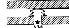
Electric power-feeding structure as become image display apparatus 105 power supplies of vacuum to inside from air has voltage to add structure 100.Image display apparatus 105 is by constituting with the lower part: panel 101, back plate 102, frame 103 are engaged, have the described vacuum tank that voltage adds structure 100; Outgoing cable 110; Drive unit 150; Voltage adds cable 161; Voltage add-on device 160.The A-A phantom of Fig. 3 presentation graphs 1.Voltage is applied on the electroconductive member 108 by through hole (below, be called the hole) 111 from the back side of back plate 102, is applied on the anode 104 by low melting material 107.The hole is the about 2mm of diameter.
The tectosome of the present application is made of electroconductive member 108, and electroconductive member 108 comprises: as the part by the pressure differential elongation, have the snake abdominal section of the part of curved shape; The part that contacts with anode; Be bonded on the part on the plate of back.Voltage adds structure 100 and is made of electroconductive member 108, low melting material 107, engagement member 109.
Temperature Influence beyond image display apparatus 105 is subjected to envisioning on every side, when being out of shape owing to thermal expansion, the close property variation of electroconductive member 108 and anode 104 sometimes.At this moment,, make its heating,, under the prerequisite that image display apparatus 105 does not disintegrate, just can improve the close property of electroconductive member 108 and anode 104 by making low melting material 107 fusings to electroconductive member 108 applying high-frequency voltages.The low melting material of fusing solidifies owing to temperature descends, and becomes the member that engages electroconductive member 108 and anode 104.
In the joint of electroconductive member 108 and back plate 102, use engagement member 109, guarantee vacuum seal.As the material of engagement member 109, for example use the frit of low-melting glass.In advance the material that has mixed frit and solvent is coated on the electroconductive member 108 with distributor, dry (for example 120 ℃, 10 minutes) carry out false sintering (for example, 360 ℃, 10 minutes).Then, in main sintering step (for example 420 ℃, 30 minutes), electroconductive member 108 is placed on the plate 102 of back, heat up on one side, used load on electroconductive member 108 makes the frit fusing of false sintering on one side, obtains good joint.
Being arranged on the state of back on the plate 102 electroconductive member down can make the interval of 101 of afterwards plate 102 and panels shortlyer from the height of back plate 102 upper surfaces.Shown in Fig. 4 (A), electroconductive member 108 engages with back plate 102 by grafting material 109.Then, shown in Fig. 4 (B), clip frame, with between back plate of sealings such as frit and the frame and between frame and the panel with back plate 102 and panel 101.Then, never illustrated blast pipe is evacuated back plate 102 and panel 101, by sealing, the vacuum tank of construction drawing image display device.At this moment, shown in Fig. 4 (C), electroconductive member 108 be the back plate through hole be the recess of hole 111 to the outside atmosphere opening, become promptly that to have in the bottom be the shape of the one side closed recess of anode, so be subjected to influence from the pressure differential of the atmospheric pressure in hole 111 and inner space, be elongated to the gap length of 101 of back plate 102 and panels, pass through low melting material 107 indirect contacts with anode 104, can realize being formed on from back plate one side direction the shape of the anode supply current potential of the electrode on the panel 101 by electroconductive member 108.Under this state, if provide current potential to electroconductive member 108, current potential just offers anode by electroconductive member 108.
Electroconductive member as the tectosome that constitutes the present application, part by a tabular component warpage being formed contact, the part of elongation with anode and with back plate engaging portion, can make the sealed engagement interface of hole 111 sealings is a place, can suppress to engage probability bad and that leak.In view of the above, can improve the rate of finished products of vacuum tank 106 and image display apparatus 105, more cheap image display apparatus 105 can be provided.In addition, be that 111 part is to the recess of outside atmosphere opening in the hole by making tectosome before the impressed pressure difference, promptly having the bottom is the shape of the one side closed recess of anode, can use the sidepiece of recess as the part of elongation, can make the length of elongation abundant.In addition,, have the tectosome of curved shape, can fully obtain the length of elongation by employing as the predetermined elongation part before the impressed pressure difference.
Embodiment
(embodiment 1)
The voltage of having made form shown in Figure 3 adds structure, have and be provided with the image display apparatus of form shown in Figure 1 of vacuum tank that this voltage adds the form illustrated in figures 1 and 2 of structure.
Make the panel 101 that is provided with anode 104 in the plane relative, sandwich frame 103 and spacing block 1002 in the centre,, made vacuum tank 106 by engaging with the back plate 102 that is provided with negative electrode 1001 in the plane.In this vacuum tank, the negative electrode in the vacuum tank, lead-out wiring (not shown) are arranged on the plate 102 of back, extend to the outside of frame 103.Negative electrode is controlled by drive unit 150 by at the logical outgoing cable 110 of its lead-out wiring terminal conductance.In addition, anode adds the voltage of structure on 100 and adds cable 161 by be installed in this voltage with connector (not shown), by 160 controls of voltage add-on device.And, can carry out these controls, pie graph image display device 105 to negative electrode and anode in the vacuum tank 106.Panel 101 and back plate 102 are formed by the glass of thickness 2.8mm.The inside of image display apparatus 105 is vacuum, uses frit (not shown) in the joint of panel 101, back plate 102 and frame 103.Coating forms claylike glass cream to frit with solvent on frame 103, makes its drying, uses stove, 420 ℃, 30min sintering, joint while pressurize.By such joint, keep the sealing of 102 of panel 101 and back plates.Image display apparatus 105 is by applied voltage on anode 104, and the negative electrode electrons emitted to vacuum from the plate 102 of back is accelerated, and is positioned at fluorophor (not shown) on the anode by bump, makes it luminous, can form visual.
Voltage adds structure 100 and is made of described electroconductive member 108, low melting material 107 and engagement member 109.The hole 111 of opening on the plate of back is diameter 2mm.
Between electroconductive member 108 and anode 104, there is low melting material 107.It has by the close property that makes electroconductive member 108 and anode 104 good, makes the good effect of conductivity.As low melting material, used low-melting metal material In alloy (140~200 ℃ of fusing points).Between electroconductive member 108 that is out of shape (elongation) owing to atmospheric pressure and anode 104, low melting material compression is close on the surface configuration of electroconductive member 108 and anode 104 (Fig. 4 (C)), can make that to conduct reliability good.
Temperature Influence beyond image display apparatus 105 is subjected to envisioning on every side, when being out of shape owing to thermal expansion, the close property variation of electroconductive member 108 and anode 104 sometimes.At this moment,, make its heating,, under the prerequisite that image display apparatus 105 does not disintegrate, just can improve the close property of electroconductive member 108 and anode 104 by making low melting material 107 fusings to electroconductive member 108 applying high-frequency voltages.
In the joint of electroconductive member 108 and back plate 102, use engagement member 109, guarantee vacuum seal.As the material of engagement member 109, for example use the frit of low-melting glass.In advance the material that has mixed frit and solvent is coated on the electroconductive member 108 with distributor, dry (for example 120 ℃, 10 minutes) carry out false sintering (for example, 360 ℃, 10 minutes).Then, in main sintering step (for example 420 ℃, 30 minutes), electroconductive member 108 is placed on the plate 102 of back, heat up on one side, used load on electroconductive member 108 makes the frit fusing of false sintering on one side, obtains good joint.
The plate of the about 10mm of diameter, thickness 0.05mm is attracted by press molding, can make this electroconductive member 108 on mould by air.When from anode 104 unilateral observation image display apparatus 105, shape is the circle of the about 4mm of overall diameter, highly about 0.7mm, and the gap length that back plate 102 and panel are 101 is shorter than 2mm.Shown in Fig. 4 A, electroconductive member 108 is bonded on the plate 102 of back by grafting material 109.Shown in Fig. 4 (b), clip frame 103 then, with between frit-sealed back plate and the frame and between frame and the panel with back plate 102 and panel 101.Then, never illustrated blast pipe is evacuated back plate 102 and 101 of panels, has made vacuum tank by sealing.At this moment, shown in Fig. 4 (C), electroconductive member 108 is owing to from the pressure differential of the pressure of the atmospheric pressure in hole 111 and inner space, be elongated to the gap length 2mm of 101 of back plate 102 and panels.Promptly poor by impressed pressure, the shape of the warpage of structural volume electroconductive member 108 for contacting with anode 104 by low melting material 107.
In electroconductive member 108, to process by pressure forming, the pars contractilis in the side produces multistage concaveconvex shape, can be controlled at the deformation direction that the atmospheric pressure of electroconductive member 108 causes the direction of anode 104.As a result, can improve the conducting reliability of electroconductive member 108 and anode 104.
(embodiment 2)
The vacuum tank of making in the present embodiment and the summary of image display apparatus replace with shown in Figure 5 but voltage adds structure similarly to Example 1.
As the electric power-feeding structure of from air, in inside becomes the image display apparatus 105 of vacuum, powering, there is voltage to add structure 100.Fig. 5 represents the cutaway view of the A-A part that is equivalent to Fig. 1 among the embodiment 2.Voltage is applied on the electroconductive member 208 by hole 111 from the back side of back plate 102, is applied on the anode 104 by low melting material 107.
Voltage adds structure 100 and is made of described electroconductive member 208, low melting material 107 and engagement member 109.The hole 111 of opening on the plate of back is diameter 2mm.
Between electroconductive member 208 and anode 104, there is low melting material 107.It has by the close property that makes electroconductive member 208 and anode 104 good, makes the good effect of conductivity.As low melting material, used low-melting metal material Sn-Pb class conjunction (180~330 ℃ of fusing points).Between electroconductive member 208 that is out of shape owing to atmospheric pressure and anode 104, low melting material compression is close on the surface configuration of electroconductive member 208 and anode 104, can make that to conduct reliability good.
Temperature Influence beyond image display apparatus 105 is subjected to envisioning on every side, when being out of shape owing to thermal expansion, the close property variation of electroconductive member 208 and anode 104 sometimes.At this moment,, make its heating,, under the prerequisite that image display apparatus 105 does not disintegrate, just can improve the close property of electroconductive member 208 and anode 104 by making low melting material 107 fusings to electroconductive member 208 applying high-frequency voltages.
In the joint of electroconductive member 208 and back plate 102, use engagement member 109, guarantee vacuum seal.As the material of engagement member 109, for example use the frit of low-melting glass.In advance the material that has mixed frit and solvent is coated on the electroconductive member 208 with distributor, dry (for example 120 ℃, 10 minutes) carry out false sintering (for example, 360 ℃, 10 minutes).Then, in main sintering step (for example 420 ℃, 30 minutes), electroconductive member 208 is placed on the plate 102 of back, heat up on one side, used load on electroconductive member 208 makes the frit fusing of false sintering on one side, obtains good joint.
The plate of the about 10mm of diameter, thickness 0.05mm is attracted by press molding, to have made this electroconductive member 208 on mould by air.When from anode 104 unilateral observation image display apparatus 105, shape is the circle of the about 4mm of overall diameter, highly about 0.7mm, and the gap length that back plate 102 and panel are 101 is shorter than 2mm.As shown in Figure 6A, electroconductive member 208 is bonded on the plate 102 of back by grafting material 109.Shown in Fig. 6 (b), clip frame 103 then, with between frit-sealed back plate and the frame and between frame and the panel with back plate 102 and panel 101.Then, never illustrated blast pipe is evacuated back plate 102 and 101 of panels, has made vacuum tank by sealing.At this moment, shown in Fig. 6 (C), electroconductive member 208 is subjected to the atmospheric influence from hole 111, is elongated to the gap length 2mm of 101 of back plate 102 and panels.In view of the above, can form by the shape of low melting material 107 with anode 104 conductings.
In electroconductive member 208, process by pressure forming, do not take the time just can produce multistage concaveconvex shape at the pars contractilis of side, can be controlled at the deformation direction that the atmospheric pressure of electroconductive member 208 causes the direction of anode 104.As a result, can improve the conducting reliability of electroconductive member 208 and anode 104.In addition, bonding part as electroconductive member 208 and back plate 102, with the face of the opposite side of face that engages by grafting material 109 and back plate 102 is outside atmosphere, but adopt the structure that is exposed in the atmospheric pressure atmosphere, adopted electroconductive member 208 with the back plate 102 the bonding part by atmospheric pressure by the structure that is pressed on back plate 102 1 sides that engage object one side, so can improve the vacuum leakproofness on composition surface.
(embodiment 3)
The vacuum tank of making in the present embodiment and the summary of image display apparatus replace with shown in Figure 7 but voltage adds structure similarly to Example 1.
As the electric power-feeding structure of from air, in inside becomes the image display apparatus 105 of vacuum, powering, there is voltage to add structure 100.Fig. 7 represents the cutaway view of the A-A part that is equivalent to Fig. 1 among the embodiment 3.Voltage is applied on the electroconductive member 308 by hole 111 from the back side of back plate 102, is applied on the anode 104 by low melting material 107.
Voltage adds structure 100 and is made of described electroconductive member 308, low melting material 107 and engagement member 109.The hole 111 of opening on the plate of back is diameter 2mm.
Between electroconductive member 308 and anode 104, there is low melting material 107.It has by the close property that makes electroconductive member 308 and anode 104 good, makes the good effect of conductivity.As low melting material, used low-melting metal material Sn-Cu alloy (200~350 ℃ of fusing points).Between electroconductive member 308 that is out of shape owing to atmospheric pressure and anode 104, low melting material compression is close on the surface configuration of electroconductive member 308 and anode 104, can make that to conduct reliability good.
Temperature Influence beyond image display apparatus 105 is subjected to envisioning on every side, when being out of shape owing to thermal expansion, the close property variation of electroconductive member 308 and anode 104 sometimes.At this moment,, make its heating,, under the prerequisite that image display apparatus 105 does not disintegrate, just can improve the close property of electroconductive member 308 and anode 104 by making low melting material 107 fusings to electroconductive member 308 applying high-frequency voltages.
In the joint of electroconductive member 308 and back plate 102, use engagement member 109, guarantee vacuum seal.As the material of engagement member 109, for example use the frit of low-melting glass.In advance the material that has mixed frit and solvent is coated on the electroconductive member 308 with distributor, dry (for example 120 ℃, 10 minutes) carry out false sintering (for example, 360 ℃, 10 minutes).Then, in main sintering step (for example 420 ℃, 30 minutes), electroconductive member 308 is placed on the plate 102 of back, heat up on one side, used load on electroconductive member 308 makes the frit fusing of false sintering on one side, obtains good joint.
The plate of the about 9mm of diameter, thickness 0.05mm is attracted by press molding, to have made this electroconductive member 308 on mould by air.When from anode 104 unilateral observation image display apparatus 105, shape is the circle of the about 4mm of overall diameter, top end diameter 0.5mm, highly about 1.5mm, and the gap length that back plate 102 and panel are 101 is shorter than 2mm.Shown in Fig. 8 A, electroconductive member 308 is bonded on the plate 102 of back by grafting material 109.Shown in Fig. 8 (b), clip frame 103 then, with between frit-sealed back plate and the frame and between frame and the panel with back plate 102 and panel 101.Then, never illustrated blast pipe is evacuated back plate 102 and 101 of panels, has made vacuum tank by sealing.At this moment, shown in Fig. 8 (C), electroconductive member 308 is subjected to the atmospheric influence from hole 111, is elongated to the gap length 2mm of 101 of back plate 102 and panels.In view of the above, can form the shape that contacts with anode 104 by low melting material 107.
Can reduce melting area, so can increase based on the pressure on the low melting material 107 of the atmospheric unit of acting on based on low melting material 107 electroconductive member 308 and 104 on anode.As a result, can improve the conducting reliability of 104 on electroconductive member 308 and anode.
(embodiment 4)
The vacuum tank that generates in the present embodiment and the summary of image display apparatus replace with shown in Figure 9 but voltage adds structure similarly to Example 1.
As the electric power-feeding structure of from air, in inside becomes the image display apparatus 105 of vacuum, powering, there is voltage to add structure 100.Fig. 9 represents the cutaway view of the A-A part that is equivalent to Fig. 1 among the embodiment 4.Voltage is applied on the electroconductive member 408 by hole 111 from the back side of back plate 102, is applied on the anode 104 by low melting material 107.
Voltage adds structure 100 and is made of described electroconductive member 408, low melting material 107 and engagement member 109.The hole 111 of opening on the plate of back is diameter 2mm.
Between electroconductive member 408 and anode 104, there is low melting material 107.It has by the close property that makes electroconductive member 408 and anode 104 good, makes the good effect of conductivity.As low melting material, used low-melting metal material Sn-Ag alloy (200~350 ℃ of fusing points), between electroconductive member 408 that is out of shape owing to atmospheric pressure and anode 104, low melting material compression, be close on the surface configuration of electroconductive member 408 and anode 104, can make that to conduct reliability good.
Temperature Influence beyond image display apparatus 105 is subjected to envisioning on every side, when being out of shape owing to thermal expansion, the close property variation of electroconductive member 408 and anode 104 sometimes.At this moment,, make its heating,, under the prerequisite that image display apparatus 105 does not disintegrate, just can improve the close property of electroconductive member 408 and anode 104 by making low melting material 107 fusings to electroconductive member 408 applying high-frequency voltages.
In the joint of electroconductive member 408 and back plate 102, use engagement member 109, guarantee vacuum seal.As the material of engagement member 109, for example use the frit of low-melting glass.In advance the material that has mixed frit and solvent is coated on the electroconductive member 408 with distributor, dry (for example 120 ℃, 10 minutes) carry out false sintering (for example, 360 ℃, 10 minutes).Then, in main sintering step (for example 420 ℃, 30 minutes), electroconductive member 408 is placed on the plate 102 of back, heat up on one side, used load on electroconductive member 408 makes the frit fusing of false sintering on one side, obtains good joint.
The plate of the about 10mm of diameter, thickness 0.15mm is attracted by press molding, to have made this electroconductive member 408 on mould by air.When from anode 104 unilateral observation image display apparatus 105, shape is the circle of the about 4mm of overall diameter, highly about 0.6mm, and the gap length that back plate 102 and panel are 101 is shorter than 2mm.Shown in Figure 10 A, electroconductive member 408 is bonded on the plate 102 of back by grafting material 109.Shown in Figure 10 (b), clip frame 103 then, with between frit-sealed back plate and the frame and between frame and the panel with back plate 102 and panel 101.Then, never illustrated blast pipe is evacuated back plate 102 and 101 of panels, has made vacuum tank by sealing.At this moment, shown in Figure 10 (C), electroconductive member 408 is subjected to the atmospheric influence from hole 111, is elongated to the gap length 2mm of 101 of back plate 102 and panels.In view of the above, can form the shape that contacts with anode 104 by low melting material 107.
Because direction in the face of back plate 102, electroconductive member 408 are circular,, can be controlled at the deformation direction of electroconductive member 408 on the direction of anode 104 so uniform atmospheric pressure takes place on circle.As a result, can improve the conducting reliability of electroconductive member 408 and anode 104.In addition, because the structure that has adopted the composition surface based on grafting material 109 of electroconductive member 408 and back plate 102 to pin by atmospheric pressure, so can improve the vacuum leakproofness on composition surface.
Claims (2)
1. the manufacture method of an airtight container, the sealing container has the space of the pressure lower than external pressure between first substrate respect to one another and second substrate, and this method comprises:
Be assembled in the number of assembling steps that has the container in space between this first substrate and second substrate, wherein be provided with electrode in the face of on the surface in described space on this first substrate, this second substrate has the tectosome that is used for supplying with to described electrode current potential; And
The poor pressure differential of exerting pressure inside and outside the container assembled in described number of assembling steps is applied step;
Wherein, in the described container before described pressure differential applies step, described tectosome has through-hole section by connecting described second substrate to the outside atmosphere opening, and recess at bottom lock, this recess has conductivity, and wherein said recess the part that is engaged in described second substrate and should with part that described electrode directly or indirectly contacts between have the face of curved shape, and, apply in described pressure differential and to produce pressure differential in the step, thereby make of the length elongation of described tectosome in described first substrate and described second substrate direction respect to one another, make described tectosome forms can provide current potential by shape from the bottom of this recess to described electrode, and the bottom of described recess directly contacts with described electrode, or the bottom of described recess contacts with described electrode by electroconductive binder, and the part that will directly or indirectly contact with described electrode of described tectosome and the part that will be out of shape of described tectosome are the parts that forms by tabular component of bending machining.
2. the manufacture method of an image display apparatus is characterized in that comprising:
The described method of claim 1 is made the step of airtight container;
The step of picture display elements is provided in the inside of airtight container.
Applications Claiming Priority (4)
| Application Number | Priority Date | Filing Date | Title |
|---|---|---|---|
| JP248839/2002 | 2002-08-28 | ||
| JP2002248839 | 2002-08-28 | ||
| JP2003296258A JP3950829B2 (en) | 2002-08-28 | 2003-08-20 | Airtight container and image display device manufacturing method |
| JP296258/2003 | 2003-08-20 |
Publications (2)
| Publication Number | Publication Date |
|---|---|
| CN1495830A CN1495830A (en) | 2004-05-12 |
| CN100514533C true CN100514533C (en) | 2009-07-15 |
Family
ID=32301246
Family Applications (1)
| Application Number | Title | Priority Date | Filing Date |
|---|---|---|---|
| CNB031553796A Expired - Fee Related CN100514533C (en) | 2002-08-28 | 2003-08-28 | Manufacturing method of sealed container, image display device thereof |
Country Status (4)
| Country | Link |
|---|---|
| US (3) | US7101244B2 (en) |
| JP (1) | JP3950829B2 (en) |
| KR (1) | KR100621531B1 (en) |
| CN (1) | CN100514533C (en) |
Families Citing this family (6)
| Publication number | Priority date | Publication date | Assignee | Title |
|---|---|---|---|---|
| JP4250608B2 (en) * | 2004-04-09 | 2009-04-08 | キヤノン株式会社 | Image display device and manufacturing method thereof |
| KR101155921B1 (en) * | 2005-10-31 | 2012-06-20 | 삼성에스디아이 주식회사 | Electron emission display device |
| JP5066859B2 (en) | 2006-07-26 | 2012-11-07 | ソニー株式会社 | Flat panel display |
| US20080315748A1 (en) * | 2007-03-30 | 2008-12-25 | Takaaki Kitada | Display Device |
| JP2009037792A (en) * | 2007-07-31 | 2009-02-19 | Hitachi Displays Ltd | Image display device |
| JP2011028977A (en) * | 2009-07-24 | 2011-02-10 | Canon Inc | Image display apparatus |
Citations (2)
| Publication number | Priority date | Publication date | Assignee | Title |
|---|---|---|---|---|
| US6114804A (en) * | 1997-03-21 | 2000-09-05 | Canon Kabushiki Kaisha | Image apparatus having recessed envelope for placement of electrode |
| US6407500B1 (en) * | 1998-08-26 | 2002-06-18 | Futaba Corporation | Electrode structure in flat vacuum envelope |
Family Cites Families (6)
| Publication number | Priority date | Publication date | Assignee | Title |
|---|---|---|---|---|
| JPH05114372A (en) | 1991-10-23 | 1993-05-07 | Sony Corp | Very thin plane display device |
| JPH0945266A (en) | 1995-07-31 | 1997-02-14 | Canon Inc | Image forming device |
| JP2000195449A (en) | 1998-12-28 | 2000-07-14 | Canon Inc | Image forming device and its manufacturing/driving method |
| US6603255B2 (en) * | 1999-02-23 | 2003-08-05 | Canon Kabushiki Kaisha | Image display unit |
| JP3684216B2 (en) * | 2001-07-31 | 2005-08-17 | キヤノン株式会社 | Display device |
| JP3768889B2 (en) * | 2002-01-31 | 2006-04-19 | キヤノン株式会社 | Display device |
-
2003
- 2003-08-20 JP JP2003296258A patent/JP3950829B2/en not_active Expired - Fee Related
- 2003-08-26 US US10/647,343 patent/US7101244B2/en not_active Expired - Fee Related
- 2003-08-28 KR KR1020030059766A patent/KR100621531B1/en not_active IP Right Cessation
- 2003-08-28 CN CNB031553796A patent/CN100514533C/en not_active Expired - Fee Related
-
2006
- 2006-05-30 US US11/442,323 patent/US7312567B2/en not_active Expired - Fee Related
-
2007
- 2007-08-20 US US11/841,043 patent/US20080278058A1/en not_active Abandoned
Patent Citations (2)
| Publication number | Priority date | Publication date | Assignee | Title |
|---|---|---|---|---|
| US6114804A (en) * | 1997-03-21 | 2000-09-05 | Canon Kabushiki Kaisha | Image apparatus having recessed envelope for placement of electrode |
| US6407500B1 (en) * | 1998-08-26 | 2002-06-18 | Futaba Corporation | Electrode structure in flat vacuum envelope |
Also Published As
| Publication number | Publication date |
|---|---|
| JP2004111376A (en) | 2004-04-08 |
| JP3950829B2 (en) | 2007-08-01 |
| CN1495830A (en) | 2004-05-12 |
| KR100621531B1 (en) | 2006-09-13 |
| US7101244B2 (en) | 2006-09-05 |
| US20060217024A1 (en) | 2006-09-28 |
| US20080278058A1 (en) | 2008-11-13 |
| US20040130259A1 (en) | 2004-07-08 |
| US7312567B2 (en) | 2007-12-25 |
| KR20040019975A (en) | 2004-03-06 |
Similar Documents
| Publication | Publication Date | Title |
|---|---|---|
| US5697825A (en) | Method for evacuating and sealing field emission displays | |
| US7249989B2 (en) | Method of manufacturing an envelope and method of manufacturing an electron beam apparatus | |
| JP3768889B2 (en) | Display device | |
| CN100514533C (en) | Manufacturing method of sealed container, image display device thereof | |
| JP3684216B2 (en) | Display device | |
| JP2001343903A (en) | Interconnecting structure of electrode, method for interconnecting electrode, image display device and method for manufacturing the same | |
| JP2004207226A (en) | Manufacturing method of image display device | |
| CN1862757B (en) | Envelope, envelope manufacturing method, image display device, and television display device | |
| JP2000315468A (en) | Image forming device | |
| JP2000208051A (en) | Sealing method, sealed container, image display device and vacuum exhaust device | |
| KR20110029081A (en) | Bonding method of base materials, and manufacturing method of image display apparatus | |
| JP3478774B2 (en) | Image display device | |
| EP2296163A2 (en) | Manufacturing method of image display apparatus, and bonding method of base material | |
| JP2004087475A (en) | Airtight container and image display device using the same | |
| CN2528105Y (en) | Lead wire for field emission display device | |
| JP4056073B2 (en) | Display device | |
| JP2000251807A (en) | Image forming device and its manufacture | |
| JP2000251793A (en) | Airtight container and image display device | |
| JPH11135041A (en) | Vacuum airtight container, display element, and power element | |
| JP2002197998A (en) | Electron beam device, image forming device and method of producing electron beam device | |
| JP2000251770A (en) | Airtight container and image forming device | |
| JP2009187825A (en) | Method of manufacturing image display device | |
| JP2002008568A (en) | Image forming device | |
| JP2004103508A (en) | Image forming device | |
| JP2003109525A (en) | Electron beam device and image forming device |
Legal Events
| Date | Code | Title | Description |
|---|---|---|---|
| C06 | Publication | ||
| PB01 | Publication | ||
| C10 | Entry into substantive examination | ||
| SE01 | Entry into force of request for substantive examination | ||
| C14 | Grant of patent or utility model | ||
| GR01 | Patent grant | ||
| CF01 | Termination of patent right due to non-payment of annual fee |
Granted publication date: 20090715 Termination date: 20140828 |
|
| EXPY | Termination of patent right or utility model |