CN100483636C - Atomic layer deposition methods - Google Patents
Atomic layer deposition methods Download PDFInfo
- Publication number
- CN100483636C CN100483636C CNB2003801086419A CN200380108641A CN100483636C CN 100483636 C CN100483636 C CN 100483636C CN B2003801086419 A CNB2003801086419 A CN B2003801086419A CN 200380108641 A CN200380108641 A CN 200380108641A CN 100483636 C CN100483636 C CN 100483636C
- Authority
- CN
- China
- Prior art keywords
- precursor gas
- monolayer
- indoor
- substrate
- plasma
- Prior art date
- Legal status (The legal status is an assumption and is not a legal conclusion. Google has not performed a legal analysis and makes no representation as to the accuracy of the status listed.)
- Expired - Lifetime
Links
- 238000000034 method Methods 0.000 title claims description 65
- 238000000231 atomic layer deposition Methods 0.000 title claims description 10
- 239000002356 single layer Substances 0.000 claims abstract description 157
- 239000002243 precursor Substances 0.000 claims abstract description 145
- 239000000758 substrate Substances 0.000 claims abstract description 67
- 239000000203 mixture Substances 0.000 claims abstract description 49
- 239000000463 material Substances 0.000 claims abstract description 22
- 230000008569 process Effects 0.000 claims description 51
- 239000004065 semiconductor Substances 0.000 claims description 14
- 238000006243 chemical reaction Methods 0.000 claims description 12
- 150000002500 ions Chemical class 0.000 claims description 7
- 230000015572 biosynthetic process Effects 0.000 claims description 6
- JLTRXTDYQLMHGR-UHFFFAOYSA-N trimethylaluminium Chemical compound C[Al](C)C JLTRXTDYQLMHGR-UHFFFAOYSA-N 0.000 claims description 5
- ATJFFYVFTNAWJD-UHFFFAOYSA-N Tin Chemical compound [Sn] ATJFFYVFTNAWJD-UHFFFAOYSA-N 0.000 claims description 2
- 239000007789 gas Substances 0.000 description 148
- 238000010926 purge Methods 0.000 description 21
- 239000010410 layer Substances 0.000 description 9
- 238000000151 deposition Methods 0.000 description 8
- 230000008021 deposition Effects 0.000 description 8
- 238000010586 diagram Methods 0.000 description 6
- 239000010936 titanium Substances 0.000 description 5
- RTAQQCXQSZGOHL-UHFFFAOYSA-N Titanium Chemical compound [Ti] RTAQQCXQSZGOHL-UHFFFAOYSA-N 0.000 description 4
- 238000005516 engineering process Methods 0.000 description 4
- 229910052719 titanium Inorganic materials 0.000 description 4
- PNEYBMLMFCGWSK-UHFFFAOYSA-N Alumina Chemical compound [O-2].[O-2].[O-2].[Al+3].[Al+3] PNEYBMLMFCGWSK-UHFFFAOYSA-N 0.000 description 3
- 239000001307 helium Substances 0.000 description 3
- 229910052734 helium Inorganic materials 0.000 description 3
- SWQJXJOGLNCZEY-UHFFFAOYSA-N helium atom Chemical compound [He] SWQJXJOGLNCZEY-UHFFFAOYSA-N 0.000 description 3
- 230000005540 biological transmission Effects 0.000 description 2
- 239000011261 inert gas Substances 0.000 description 2
- 239000002184 metal Substances 0.000 description 2
- 229910052751 metal Inorganic materials 0.000 description 2
- 238000002360 preparation method Methods 0.000 description 2
- 239000000126 substance Substances 0.000 description 2
- 229910017107 AlOx Inorganic materials 0.000 description 1
- 101100425947 Mus musculus Tnfrsf13b gene Proteins 0.000 description 1
- 230000004913 activation Effects 0.000 description 1
- 238000001994 activation Methods 0.000 description 1
- 125000004429 atom Chemical group 0.000 description 1
- 239000006227 byproduct Substances 0.000 description 1
- 239000007795 chemical reaction product Substances 0.000 description 1
- 229910052801 chlorine Inorganic materials 0.000 description 1
- 125000001309 chloro group Chemical group Cl* 0.000 description 1
- 239000000470 constituent Substances 0.000 description 1
- 239000003989 dielectric material Substances 0.000 description 1
- 239000006185 dispersion Substances 0.000 description 1
- 238000010336 energy treatment Methods 0.000 description 1
- 238000010438 heat treatment Methods 0.000 description 1
- 230000006698 induction Effects 0.000 description 1
- 238000003780 insertion Methods 0.000 description 1
- 230000037431 insertion Effects 0.000 description 1
- 238000009434 installation Methods 0.000 description 1
- 238000009413 insulation Methods 0.000 description 1
- 229910000765 intermetallic Inorganic materials 0.000 description 1
- 238000003754 machining Methods 0.000 description 1
- 230000013011 mating Effects 0.000 description 1
- 230000007246 mechanism Effects 0.000 description 1
- 239000007769 metal material Substances 0.000 description 1
- 230000035515 penetration Effects 0.000 description 1
- 238000000197 pyrolysis Methods 0.000 description 1
- 230000002285 radioactive effect Effects 0.000 description 1
- 239000000376 reactant Substances 0.000 description 1
- 230000009467 reduction Effects 0.000 description 1
- 229910052715 tantalum Inorganic materials 0.000 description 1
- GUVRBAGPIYLISA-UHFFFAOYSA-N tantalum atom Chemical compound [Ta] GUVRBAGPIYLISA-UHFFFAOYSA-N 0.000 description 1
- 238000007725 thermal activation Methods 0.000 description 1
- 230000009466 transformation Effects 0.000 description 1
Images


Classifications
-
- H—ELECTRICITY
- H01—ELECTRIC ELEMENTS
- H01L—SEMICONDUCTOR DEVICES NOT COVERED BY CLASS H10
- H01L21/00—Processes or apparatus adapted for the manufacture or treatment of semiconductor or solid state devices or of parts thereof
- H01L21/02—Manufacture or treatment of semiconductor devices or of parts thereof
- H01L21/04—Manufacture or treatment of semiconductor devices or of parts thereof the devices having at least one potential-jump barrier or surface barrier, e.g. PN junction, depletion layer or carrier concentration layer
- H01L21/18—Manufacture or treatment of semiconductor devices or of parts thereof the devices having at least one potential-jump barrier or surface barrier, e.g. PN junction, depletion layer or carrier concentration layer the devices having semiconductor bodies comprising elements of Group IV of the Periodic System or AIIIBV compounds with or without impurities, e.g. doping materials
- H01L21/20—Deposition of semiconductor materials on a substrate, e.g. epitaxial growth solid phase epitaxy
-
- C—CHEMISTRY; METALLURGY
- C23—COATING METALLIC MATERIAL; COATING MATERIAL WITH METALLIC MATERIAL; CHEMICAL SURFACE TREATMENT; DIFFUSION TREATMENT OF METALLIC MATERIAL; COATING BY VACUUM EVAPORATION, BY SPUTTERING, BY ION IMPLANTATION OR BY CHEMICAL VAPOUR DEPOSITION, IN GENERAL; INHIBITING CORROSION OF METALLIC MATERIAL OR INCRUSTATION IN GENERAL
- C23C—COATING METALLIC MATERIAL; COATING MATERIAL WITH METALLIC MATERIAL; SURFACE TREATMENT OF METALLIC MATERIAL BY DIFFUSION INTO THE SURFACE, BY CHEMICAL CONVERSION OR SUBSTITUTION; COATING BY VACUUM EVAPORATION, BY SPUTTERING, BY ION IMPLANTATION OR BY CHEMICAL VAPOUR DEPOSITION, IN GENERAL
- C23C16/00—Chemical coating by decomposition of gaseous compounds, without leaving reaction products of surface material in the coating, i.e. chemical vapour deposition [CVD] processes
- C23C16/22—Chemical coating by decomposition of gaseous compounds, without leaving reaction products of surface material in the coating, i.e. chemical vapour deposition [CVD] processes characterised by the deposition of inorganic material, other than metallic material
- C23C16/30—Deposition of compounds, mixtures or solid solutions, e.g. borides, carbides, nitrides
- C23C16/38—Borides
-
- C—CHEMISTRY; METALLURGY
- C23—COATING METALLIC MATERIAL; COATING MATERIAL WITH METALLIC MATERIAL; CHEMICAL SURFACE TREATMENT; DIFFUSION TREATMENT OF METALLIC MATERIAL; COATING BY VACUUM EVAPORATION, BY SPUTTERING, BY ION IMPLANTATION OR BY CHEMICAL VAPOUR DEPOSITION, IN GENERAL; INHIBITING CORROSION OF METALLIC MATERIAL OR INCRUSTATION IN GENERAL
- C23C—COATING METALLIC MATERIAL; COATING MATERIAL WITH METALLIC MATERIAL; SURFACE TREATMENT OF METALLIC MATERIAL BY DIFFUSION INTO THE SURFACE, BY CHEMICAL CONVERSION OR SUBSTITUTION; COATING BY VACUUM EVAPORATION, BY SPUTTERING, BY ION IMPLANTATION OR BY CHEMICAL VAPOUR DEPOSITION, IN GENERAL
- C23C16/00—Chemical coating by decomposition of gaseous compounds, without leaving reaction products of surface material in the coating, i.e. chemical vapour deposition [CVD] processes
- C23C16/22—Chemical coating by decomposition of gaseous compounds, without leaving reaction products of surface material in the coating, i.e. chemical vapour deposition [CVD] processes characterised by the deposition of inorganic material, other than metallic material
- C23C16/30—Deposition of compounds, mixtures or solid solutions, e.g. borides, carbides, nitrides
- C23C16/40—Oxides
- C23C16/403—Oxides of aluminium, magnesium or beryllium
-
- C—CHEMISTRY; METALLURGY
- C23—COATING METALLIC MATERIAL; COATING MATERIAL WITH METALLIC MATERIAL; CHEMICAL SURFACE TREATMENT; DIFFUSION TREATMENT OF METALLIC MATERIAL; COATING BY VACUUM EVAPORATION, BY SPUTTERING, BY ION IMPLANTATION OR BY CHEMICAL VAPOUR DEPOSITION, IN GENERAL; INHIBITING CORROSION OF METALLIC MATERIAL OR INCRUSTATION IN GENERAL
- C23C—COATING METALLIC MATERIAL; COATING MATERIAL WITH METALLIC MATERIAL; SURFACE TREATMENT OF METALLIC MATERIAL BY DIFFUSION INTO THE SURFACE, BY CHEMICAL CONVERSION OR SUBSTITUTION; COATING BY VACUUM EVAPORATION, BY SPUTTERING, BY ION IMPLANTATION OR BY CHEMICAL VAPOUR DEPOSITION, IN GENERAL
- C23C16/00—Chemical coating by decomposition of gaseous compounds, without leaving reaction products of surface material in the coating, i.e. chemical vapour deposition [CVD] processes
- C23C16/44—Chemical coating by decomposition of gaseous compounds, without leaving reaction products of surface material in the coating, i.e. chemical vapour deposition [CVD] processes characterised by the method of coating
- C23C16/455—Chemical coating by decomposition of gaseous compounds, without leaving reaction products of surface material in the coating, i.e. chemical vapour deposition [CVD] processes characterised by the method of coating characterised by the method used for introducing gases into reaction chamber or for modifying gas flows in reaction chamber
- C23C16/45523—Pulsed gas flow or change of composition over time
- C23C16/45525—Atomic layer deposition [ALD]
- C23C16/45527—Atomic layer deposition [ALD] characterized by the ALD cycle, e.g. different flows or temperatures during half-reactions, unusual pulsing sequence, use of precursor mixtures or auxiliary reactants or activations
- C23C16/45536—Use of plasma, radiation or electromagnetic fields
- C23C16/45542—Plasma being used non-continuously during the ALD reactions
-
- C—CHEMISTRY; METALLURGY
- C23—COATING METALLIC MATERIAL; COATING MATERIAL WITH METALLIC MATERIAL; CHEMICAL SURFACE TREATMENT; DIFFUSION TREATMENT OF METALLIC MATERIAL; COATING BY VACUUM EVAPORATION, BY SPUTTERING, BY ION IMPLANTATION OR BY CHEMICAL VAPOUR DEPOSITION, IN GENERAL; INHIBITING CORROSION OF METALLIC MATERIAL OR INCRUSTATION IN GENERAL
- C23C—COATING METALLIC MATERIAL; COATING MATERIAL WITH METALLIC MATERIAL; SURFACE TREATMENT OF METALLIC MATERIAL BY DIFFUSION INTO THE SURFACE, BY CHEMICAL CONVERSION OR SUBSTITUTION; COATING BY VACUUM EVAPORATION, BY SPUTTERING, BY ION IMPLANTATION OR BY CHEMICAL VAPOUR DEPOSITION, IN GENERAL
- C23C16/00—Chemical coating by decomposition of gaseous compounds, without leaving reaction products of surface material in the coating, i.e. chemical vapour deposition [CVD] processes
- C23C16/44—Chemical coating by decomposition of gaseous compounds, without leaving reaction products of surface material in the coating, i.e. chemical vapour deposition [CVD] processes characterised by the method of coating
- C23C16/50—Chemical coating by decomposition of gaseous compounds, without leaving reaction products of surface material in the coating, i.e. chemical vapour deposition [CVD] processes characterised by the method of coating using electric discharges
- C23C16/515—Chemical coating by decomposition of gaseous compounds, without leaving reaction products of surface material in the coating, i.e. chemical vapour deposition [CVD] processes characterised by the method of coating using electric discharges using pulsed discharges
-
- H—ELECTRICITY
- H01—ELECTRIC ELEMENTS
- H01L—SEMICONDUCTOR DEVICES NOT COVERED BY CLASS H10
- H01L21/00—Processes or apparatus adapted for the manufacture or treatment of semiconductor or solid state devices or of parts thereof
- H01L21/02—Manufacture or treatment of semiconductor devices or of parts thereof
- H01L21/02104—Forming layers
- H01L21/02107—Forming insulating materials on a substrate
- H01L21/02225—Forming insulating materials on a substrate characterised by the process for the formation of the insulating layer
- H01L21/0226—Forming insulating materials on a substrate characterised by the process for the formation of the insulating layer formation by a deposition process
- H01L21/02263—Forming insulating materials on a substrate characterised by the process for the formation of the insulating layer formation by a deposition process deposition from the gas or vapour phase
- H01L21/02271—Forming insulating materials on a substrate characterised by the process for the formation of the insulating layer formation by a deposition process deposition from the gas or vapour phase deposition by decomposition or reaction of gaseous or vapour phase compounds, i.e. chemical vapour deposition
- H01L21/02274—Forming insulating materials on a substrate characterised by the process for the formation of the insulating layer formation by a deposition process deposition from the gas or vapour phase deposition by decomposition or reaction of gaseous or vapour phase compounds, i.e. chemical vapour deposition in the presence of a plasma [PECVD]
-
- H—ELECTRICITY
- H01—ELECTRIC ELEMENTS
- H01L—SEMICONDUCTOR DEVICES NOT COVERED BY CLASS H10
- H01L21/00—Processes or apparatus adapted for the manufacture or treatment of semiconductor or solid state devices or of parts thereof
- H01L21/02—Manufacture or treatment of semiconductor devices or of parts thereof
- H01L21/02104—Forming layers
- H01L21/02107—Forming insulating materials on a substrate
- H01L21/02225—Forming insulating materials on a substrate characterised by the process for the formation of the insulating layer
- H01L21/0226—Forming insulating materials on a substrate characterised by the process for the formation of the insulating layer formation by a deposition process
- H01L21/02263—Forming insulating materials on a substrate characterised by the process for the formation of the insulating layer formation by a deposition process deposition from the gas or vapour phase
- H01L21/02271—Forming insulating materials on a substrate characterised by the process for the formation of the insulating layer formation by a deposition process deposition from the gas or vapour phase deposition by decomposition or reaction of gaseous or vapour phase compounds, i.e. chemical vapour deposition
- H01L21/0228—Forming insulating materials on a substrate characterised by the process for the formation of the insulating layer formation by a deposition process deposition from the gas or vapour phase deposition by decomposition or reaction of gaseous or vapour phase compounds, i.e. chemical vapour deposition deposition by cyclic CVD, e.g. ALD, ALE, pulsed CVD
-
- H—ELECTRICITY
- H01—ELECTRIC ELEMENTS
- H01L—SEMICONDUCTOR DEVICES NOT COVERED BY CLASS H10
- H01L21/00—Processes or apparatus adapted for the manufacture or treatment of semiconductor or solid state devices or of parts thereof
- H01L21/02—Manufacture or treatment of semiconductor devices or of parts thereof
- H01L21/04—Manufacture or treatment of semiconductor devices or of parts thereof the devices having at least one potential-jump barrier or surface barrier, e.g. PN junction, depletion layer or carrier concentration layer
- H01L21/18—Manufacture or treatment of semiconductor devices or of parts thereof the devices having at least one potential-jump barrier or surface barrier, e.g. PN junction, depletion layer or carrier concentration layer the devices having semiconductor bodies comprising elements of Group IV of the Periodic System or AIIIBV compounds with or without impurities, e.g. doping materials
- H01L21/28—Manufacture of electrodes on semiconductor bodies using processes or apparatus not provided for in groups H01L21/20 - H01L21/268
- H01L21/283—Deposition of conductive or insulating materials for electrodes conducting electric current
- H01L21/285—Deposition of conductive or insulating materials for electrodes conducting electric current from a gas or vapour, e.g. condensation
- H01L21/28506—Deposition of conductive or insulating materials for electrodes conducting electric current from a gas or vapour, e.g. condensation of conductive layers
- H01L21/28512—Deposition of conductive or insulating materials for electrodes conducting electric current from a gas or vapour, e.g. condensation of conductive layers on semiconductor bodies comprising elements of Group IV of the Periodic System
- H01L21/28556—Deposition of conductive or insulating materials for electrodes conducting electric current from a gas or vapour, e.g. condensation of conductive layers on semiconductor bodies comprising elements of Group IV of the Periodic System by chemical means, e.g. CVD, LPCVD, PECVD, laser CVD
- H01L21/28562—Selective deposition
-
- H—ELECTRICITY
- H01—ELECTRIC ELEMENTS
- H01L—SEMICONDUCTOR DEVICES NOT COVERED BY CLASS H10
- H01L21/00—Processes or apparatus adapted for the manufacture or treatment of semiconductor or solid state devices or of parts thereof
- H01L21/02—Manufacture or treatment of semiconductor devices or of parts thereof
- H01L21/04—Manufacture or treatment of semiconductor devices or of parts thereof the devices having at least one potential-jump barrier or surface barrier, e.g. PN junction, depletion layer or carrier concentration layer
- H01L21/18—Manufacture or treatment of semiconductor devices or of parts thereof the devices having at least one potential-jump barrier or surface barrier, e.g. PN junction, depletion layer or carrier concentration layer the devices having semiconductor bodies comprising elements of Group IV of the Periodic System or AIIIBV compounds with or without impurities, e.g. doping materials
- H01L21/30—Treatment of semiconductor bodies using processes or apparatus not provided for in groups H01L21/20 - H01L21/26
- H01L21/31—Treatment of semiconductor bodies using processes or apparatus not provided for in groups H01L21/20 - H01L21/26 to form insulating layers thereon, e.g. for masking or by using photolithographic techniques; After treatment of these layers; Selection of materials for these layers
- H01L21/314—Inorganic layers
- H01L21/3141—Deposition using atomic layer deposition techniques [ALD]
-
- H—ELECTRICITY
- H01—ELECTRIC ELEMENTS
- H01L—SEMICONDUCTOR DEVICES NOT COVERED BY CLASS H10
- H01L21/00—Processes or apparatus adapted for the manufacture or treatment of semiconductor or solid state devices or of parts thereof
- H01L21/70—Manufacture or treatment of devices consisting of a plurality of solid state components formed in or on a common substrate or of parts thereof; Manufacture of integrated circuit devices or of parts thereof
- H01L21/71—Manufacture of specific parts of devices defined in group H01L21/70
- H01L21/768—Applying interconnections to be used for carrying current between separate components within a device comprising conductors and dielectrics
- H01L21/76838—Applying interconnections to be used for carrying current between separate components within a device comprising conductors and dielectrics characterised by the formation and the after-treatment of the conductors
- H01L21/76841—Barrier, adhesion or liner layers
-
- H—ELECTRICITY
- H01—ELECTRIC ELEMENTS
- H01L—SEMICONDUCTOR DEVICES NOT COVERED BY CLASS H10
- H01L21/00—Processes or apparatus adapted for the manufacture or treatment of semiconductor or solid state devices or of parts thereof
- H01L21/02—Manufacture or treatment of semiconductor devices or of parts thereof
- H01L21/02104—Forming layers
- H01L21/02107—Forming insulating materials on a substrate
- H01L21/02109—Forming insulating materials on a substrate characterised by the type of layer, e.g. type of material, porous/non-porous, pre-cursors, mixtures or laminates
- H01L21/02112—Forming insulating materials on a substrate characterised by the type of layer, e.g. type of material, porous/non-porous, pre-cursors, mixtures or laminates characterised by the material of the layer
- H01L21/02172—Forming insulating materials on a substrate characterised by the type of layer, e.g. type of material, porous/non-porous, pre-cursors, mixtures or laminates characterised by the material of the layer the material containing at least one metal element, e.g. metal oxides, metal nitrides, metal oxynitrides or metal carbides
- H01L21/02175—Forming insulating materials on a substrate characterised by the type of layer, e.g. type of material, porous/non-porous, pre-cursors, mixtures or laminates characterised by the material of the layer the material containing at least one metal element, e.g. metal oxides, metal nitrides, metal oxynitrides or metal carbides characterised by the metal
- H01L21/02178—Forming insulating materials on a substrate characterised by the type of layer, e.g. type of material, porous/non-porous, pre-cursors, mixtures or laminates characterised by the material of the layer the material containing at least one metal element, e.g. metal oxides, metal nitrides, metal oxynitrides or metal carbides characterised by the metal the material containing aluminium, e.g. Al2O3
-
- H—ELECTRICITY
- H01—ELECTRIC ELEMENTS
- H01L—SEMICONDUCTOR DEVICES NOT COVERED BY CLASS H10
- H01L21/00—Processes or apparatus adapted for the manufacture or treatment of semiconductor or solid state devices or of parts thereof
- H01L21/02—Manufacture or treatment of semiconductor devices or of parts thereof
- H01L21/02104—Forming layers
- H01L21/02107—Forming insulating materials on a substrate
- H01L21/02109—Forming insulating materials on a substrate characterised by the type of layer, e.g. type of material, porous/non-porous, pre-cursors, mixtures or laminates
- H01L21/02112—Forming insulating materials on a substrate characterised by the type of layer, e.g. type of material, porous/non-porous, pre-cursors, mixtures or laminates characterised by the material of the layer
- H01L21/02172—Forming insulating materials on a substrate characterised by the type of layer, e.g. type of material, porous/non-porous, pre-cursors, mixtures or laminates characterised by the material of the layer the material containing at least one metal element, e.g. metal oxides, metal nitrides, metal oxynitrides or metal carbides
- H01L21/02175—Forming insulating materials on a substrate characterised by the type of layer, e.g. type of material, porous/non-porous, pre-cursors, mixtures or laminates characterised by the material of the layer the material containing at least one metal element, e.g. metal oxides, metal nitrides, metal oxynitrides or metal carbides characterised by the metal
- H01L21/02183—Forming insulating materials on a substrate characterised by the type of layer, e.g. type of material, porous/non-porous, pre-cursors, mixtures or laminates characterised by the material of the layer the material containing at least one metal element, e.g. metal oxides, metal nitrides, metal oxynitrides or metal carbides characterised by the metal the material containing tantalum, e.g. Ta2O5
-
- H—ELECTRICITY
- H01—ELECTRIC ELEMENTS
- H01L—SEMICONDUCTOR DEVICES NOT COVERED BY CLASS H10
- H01L21/00—Processes or apparatus adapted for the manufacture or treatment of semiconductor or solid state devices or of parts thereof
- H01L21/02—Manufacture or treatment of semiconductor devices or of parts thereof
- H01L21/02104—Forming layers
- H01L21/02107—Forming insulating materials on a substrate
- H01L21/02109—Forming insulating materials on a substrate characterised by the type of layer, e.g. type of material, porous/non-porous, pre-cursors, mixtures or laminates
- H01L21/02112—Forming insulating materials on a substrate characterised by the type of layer, e.g. type of material, porous/non-porous, pre-cursors, mixtures or laminates characterised by the material of the layer
- H01L21/02172—Forming insulating materials on a substrate characterised by the type of layer, e.g. type of material, porous/non-porous, pre-cursors, mixtures or laminates characterised by the material of the layer the material containing at least one metal element, e.g. metal oxides, metal nitrides, metal oxynitrides or metal carbides
- H01L21/02175—Forming insulating materials on a substrate characterised by the type of layer, e.g. type of material, porous/non-porous, pre-cursors, mixtures or laminates characterised by the material of the layer the material containing at least one metal element, e.g. metal oxides, metal nitrides, metal oxynitrides or metal carbides characterised by the metal
- H01L21/02186—Forming insulating materials on a substrate characterised by the type of layer, e.g. type of material, porous/non-porous, pre-cursors, mixtures or laminates characterised by the material of the layer the material containing at least one metal element, e.g. metal oxides, metal nitrides, metal oxynitrides or metal carbides characterised by the metal the material containing titanium, e.g. TiO2
-
- H—ELECTRICITY
- H01—ELECTRIC ELEMENTS
- H01L—SEMICONDUCTOR DEVICES NOT COVERED BY CLASS H10
- H01L21/00—Processes or apparatus adapted for the manufacture or treatment of semiconductor or solid state devices or of parts thereof
- H01L21/02—Manufacture or treatment of semiconductor devices or of parts thereof
- H01L21/02104—Forming layers
- H01L21/02107—Forming insulating materials on a substrate
- H01L21/02109—Forming insulating materials on a substrate characterised by the type of layer, e.g. type of material, porous/non-porous, pre-cursors, mixtures or laminates
- H01L21/02205—Forming insulating materials on a substrate characterised by the type of layer, e.g. type of material, porous/non-porous, pre-cursors, mixtures or laminates the layer being characterised by the precursor material for deposition
-
- H—ELECTRICITY
- H01—ELECTRIC ELEMENTS
- H01L—SEMICONDUCTOR DEVICES NOT COVERED BY CLASS H10
- H01L21/00—Processes or apparatus adapted for the manufacture or treatment of semiconductor or solid state devices or of parts thereof
- H01L21/02—Manufacture or treatment of semiconductor devices or of parts thereof
- H01L21/04—Manufacture or treatment of semiconductor devices or of parts thereof the devices having at least one potential-jump barrier or surface barrier, e.g. PN junction, depletion layer or carrier concentration layer
- H01L21/18—Manufacture or treatment of semiconductor devices or of parts thereof the devices having at least one potential-jump barrier or surface barrier, e.g. PN junction, depletion layer or carrier concentration layer the devices having semiconductor bodies comprising elements of Group IV of the Periodic System or AIIIBV compounds with or without impurities, e.g. doping materials
- H01L21/30—Treatment of semiconductor bodies using processes or apparatus not provided for in groups H01L21/20 - H01L21/26
- H01L21/31—Treatment of semiconductor bodies using processes or apparatus not provided for in groups H01L21/20 - H01L21/26 to form insulating layers thereon, e.g. for masking or by using photolithographic techniques; After treatment of these layers; Selection of materials for these layers
- H01L21/314—Inorganic layers
- H01L21/316—Inorganic layers composed of oxides or glassy oxides or oxide based glass
- H01L21/31604—Deposition from a gas or vapour
- H01L21/31616—Deposition of Al2O3
-
- H—ELECTRICITY
- H01—ELECTRIC ELEMENTS
- H01L—SEMICONDUCTOR DEVICES NOT COVERED BY CLASS H10
- H01L21/00—Processes or apparatus adapted for the manufacture or treatment of semiconductor or solid state devices or of parts thereof
- H01L21/02—Manufacture or treatment of semiconductor devices or of parts thereof
- H01L21/04—Manufacture or treatment of semiconductor devices or of parts thereof the devices having at least one potential-jump barrier or surface barrier, e.g. PN junction, depletion layer or carrier concentration layer
- H01L21/18—Manufacture or treatment of semiconductor devices or of parts thereof the devices having at least one potential-jump barrier or surface barrier, e.g. PN junction, depletion layer or carrier concentration layer the devices having semiconductor bodies comprising elements of Group IV of the Periodic System or AIIIBV compounds with or without impurities, e.g. doping materials
- H01L21/30—Treatment of semiconductor bodies using processes or apparatus not provided for in groups H01L21/20 - H01L21/26
- H01L21/31—Treatment of semiconductor bodies using processes or apparatus not provided for in groups H01L21/20 - H01L21/26 to form insulating layers thereon, e.g. for masking or by using photolithographic techniques; After treatment of these layers; Selection of materials for these layers
- H01L21/314—Inorganic layers
- H01L21/316—Inorganic layers composed of oxides or glassy oxides or oxide based glass
- H01L21/3165—Inorganic layers composed of oxides or glassy oxides or oxide based glass formed by oxidation
- H01L21/31683—Inorganic layers composed of oxides or glassy oxides or oxide based glass formed by oxidation of metallic layers, e.g. Al deposited on the body, e.g. formation of multi-layer insulating structures
Abstract
A first precursor gas is flowed to the substrate within the chamber effective to form a first monolayer on the substrate. A second precursor gas different in composition from the first precursor gas is flowed to the first monolayer within the chamber under surface microwave plasma conditions within the chamber effective to react with the first monolayer and form a second monolayer on the substrate which is different in composition from the first monolayer. The second monolayer includes components of the first monolayer and the second precursor. In one implementation, the first and second precursor flowings are successively repeated effective to form a mass of material on the substrate of the second monolayer composition. Additional and other implementations are contemplated.
Description
Technical field
The present invention relates to Atomic layer deposition method.
Background technology
In integrated circuit was made, semiconductor machining was usually included in sedimentary deposit at the semiconductor-based end.A kind of such method is ald (ALD), and it relates in a settling chamber, the continuous monolayer of deposition in described substrate, and described chamber maintains under the negative pressure usually.For the ALD of routine,, make continuous monoatomic layer be adsorbed onto in the described substrate and/or with described suprabasil outer reaction usually by different deposition precursor things (precursor) is continuously fed on the substrate surface.
Make a kind of single, vaporized predecessor be fed to the settling chamber and form first monolayer effectively in substrate thereby a kind of representative ALD method comprises, described substrate is installed in described indoor.Then, stop flowing of the first deposition precursor thing, make a kind of inactive purge gases flow through described chamber, thereby from described chamber, do not remove any effectively attached to first described substrate, the remaining predecessor.Subsequently, make the second steam deposition precursor logistics different to described chamber with the first steam predecessor, thereby/second monolayer formed effectively on described first monolayer.Described second monolayer can be with described first monolayer reaction.Other predecessor can form continuous monolayer, perhaps can repeat said process up to the layer that has formed expectation thickness and composition in described substrate.
The disclosed another kind of formation film process of WO0245871 is the ald of ion induction.Be different from heating or pyrolysis, do not adopt the thermal activation energy in this method.Particularly, ald reacts by the energy drives that comes from knock-on ion, and its intermediate ion is used to by chain collision required activation energy be delivered near surperficial atom and absorbed reactant.This technology can make substrate remain on lower temperature.
The disclosed another kind of technique for atomic layer deposition of WO0243114 is the ald that plasma strengthens.The predecessor that this technology using plasma excites is to be used for deposition reaction or to improve material by plasma bombardment.
General introduction
The present invention includes Atomic layer deposition method.In one embodiment, to be positioned at ald indoor at the semiconductor-based end.Make first precursor gas (precursor gas) flow to described indoor substrate, thereby in described substrate, form first monolayer effectively.Described indoor, under the surface microwave plasma condition, make second precursor gas different flow to the described first indoor monolayer with first precursor gas composition, thereby make it effectively with described first monolayer reaction, and in described substrate, forming second monolayer, described second monolayer is different with the composition of described first monolayer.Described second monolayer comprises the composition of described first monolayer and second precursor gas.In one embodiment, thus repeat flowing in described substrate, to form effectively and having the lot of materials (a mass of material) that second monolayer is formed of described first and second precursor gas continuously.In one embodiment, after second front drive gas flow, make three precursor gas different flow to the described second indoor monolayer with first and second precursor gas composition, thereby effectively with the reaction of described second monolayer and form the 3rd monolayer in described substrate, described the 3rd monolayer is different with the composition of described first and second monolayers.In one embodiment, after second front drive gas flow, make first precursor gas flow to described indoor substrate, thereby make it effectively with described second monolayer reaction, and the composition of a) removing described second monolayer, thereby form the 3rd monolayer of forming in described substrate, the described the 3rd monolayer of forming is different with the composition of described first and second monolayers; B) on the described the 3rd monolayer of forming, form the 4th monolayer with first monolayer composition.
Imagine and disclose other aspect and execution mode, described aspect needn't be similar with above-mentioned either side and process with process.
Brief description of drawings
With reference to following accompanying drawing the preferred embodiments of the invention are described below.
Fig. 1 is the profile that is used for according to the exemplary atomic layer deposition apparatus usable of one aspect of the invention.
Fig. 2 is according to a series of diagrammatic molecular level views one aspect of the invention, a kind of exemplary process.
Fig. 3 is according to a series of diagrammatic molecular level views one aspect of the invention, a kind of exemplary process.
Fig. 4 is according to a series of diagrammatic molecular level views one aspect of the invention, a kind of exemplary process.
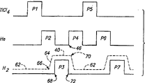
Fig. 5 is a series of conventional timelines, and it shows the representative air-flow and the power level (power level) of a kind of technical process of representative aspect according to the present invention.
Fig. 6 is the conventional timeline (timeline) of the alternate series of timeline shown in Figure 5.
Fig. 7 is the conventional timeline of another alternate series of timeline shown in Figure 5.
Fig. 8 also is the conventional timeline of another alternate series of timeline shown in Figure 5.
Fig. 9 still is the conventional timeline of another alternate series of timeline shown in Figure 5.
Figure 10 is the conventional timeline of another alternate series of timeline shown in Figure 5.
With doing the best mode of realizing the present invention and the disclosure of invention
Fig. 1 has described a kind of exemplary atomic layer deposition apparatus usable that is used for according to one aspect of the invention.This device can produce surface microwave plasma in the chamber, in described chamber, with respect to carrying out ald in the semiconductor-based end. in the context of this document, " surface microwave plasma " is defined as a kind of plasma that produces in the gas of collision substrate, by from a plurality of dispersions, the described substrate of microwave energy treatment of the microwave rf generator emission of isolating, and no matter it is to carry out in existing mode or in the mode that requires study. a kind of existing mode uses a kind of antenna for example to be surface plane antenna (SPA) or a kind of radioactive ray notch antenna (RLSA) for passing through. only for instance, can be in U.S. Patent No. 6,399,520, with 6,343,565 find described example, at this with reference to using its disclosed content.
Device 10 is described as comprising settling chamber 12 by diagram, and described settling chamber 12 is provided with the semiconductor-based end 14.In the context of this document, term " the semiconductor-based end " or " semiconductive substrate " be defined as mean any structure that comprises semi-conducting material, it comprises but is not limited to for example semiconductor wafer (separately wafer or to contain the assembly of other material thereon) of bulk semiconductive materials, semiconductor material layer (individual layer or to contain the assembly of other material thereon). term " substrate " is meant any supporting structure, it comprises but is not limited to the above-mentioned semiconductor-based end. provide a kind of suitable supporting or mechanism's (not shown) to be used to support wherein substrate 14, it can be controlled with temperature, power is handled and/or the alternate manner structure, to be used for that substrate 14 is arranged on chamber 12 as expectation.
Suitable microwave generator 16 is connected effectively with surface plane antenna 18, described antenna 18 is installed in directly over the settling chamber 12. normally, surface plane antenna 18 is made up of a kind of metal material, it has a plurality of microwave emission ports 20 that are formed on wherein, the microwave energy that is produced by source 16 is delivered in the chamber 12 by described emission port, and press close to the surface of substrate 14. therefore, roof of the chamber 12 of installation surface flat plane antenna 18 also is provided as the transmission microwave on it. certainly, some or all surface flat plane antenna 18 can be provided in the settling chamber 12. the representative preferred distance from the upper surface of substrate 13 to the lower surface of second antenna 28 is that 65mm. can use greater or lesser spacing certainly. in some cases, can use the spacing more much smaller than 65mm. in addition, except that microwave, also imagines energy produced with microwave energy and produce combination, and no matter it is 12 outside in chamber 12 or in the chamber.
Exemplary precursor gas that diagram shows and/or Purge gas inlet 22 and 24 are used for precursor gas and/or Purge gas are transmitted between the substrate 14 and surface plane antenna 18 in the chamber 12.The vacuum droop line 26 that diagram shows is used for 26 emission of substance from the chamber. and the device of Fig. 1 structurally only is a diagrammatic and representational, any other suitable device can be used for the method according to this invention aspect. for example, certainly also can imagine any alternative structure such as shower nozzle, multiport or other device, no matter and described structure is existing or requires study, be used to make gas to arrive described chamber and from described chamber emission of substance.
It is indoor that a kind of semiconductor-based end is arranged on a kind of ald as substrate 14. make first precursor gas flow to as described in indoor substrate, for example by inlet one or two in 22 and 24, thereby in described substrate, form first monolayer effectively.Only for instance, about forming the representative TiB of one deck
2Layer, a kind of representative first precursor gas comprises TiCl
4, and for example it is used in combination separately or with inertia or other gas. and a kind of for example by TiCl
4Representativeness first monolayer of preparation is TiCl
x, it is for example the same as described in Figure 2. and Fig. 2 has illustrated at a kind of use TiCl
4Atomic layer deposition method in the representativeness course of processing according to the order of sequence. Fig. 2 has described a kind of suitable substrate surface 30 than the declaratives on the left side, is attached with to comprise TiCl on described surperficial 30
x First monolayer 32. only for instance, it has such form, titanium adheres on the substrate surface 30, chlorine atom or molecule stretch out from described titanium.
Normally, use a kind of inactive purge gases then or pass through some other methods, any remaining first precursor gas is discharged from described chamber. in any case, then described indoor, under the surface microwave plasma condition, make composition second precursor gas different flow to the described first indoor monolayer with first precursor gas, thereby make it effectively to react and formation second monolayer in described substrate with first monolayer, the composition of described second monolayer is different with described first monolayer, described second monolayer comprises the composition of described first monolayer and second precursor gas. in the context of this document, a kind of " forming different " gas means that the gas that compares with it compares, and some gases have and substitute and/or additional reacted constituent.
The medial view of Fig. 2 has been described a kind of preferred representative second precursor gas, and it comprises B
2H
6, and under the surface microwave plasma condition, be in activated state. as described at right figure, it with 32 reactions of first monolayer, comprises TiB thereby form effectively
2 Second monolayer 34, and have byproduct HCl. second monolayer 34 and comprise the composition (being Ti) of described first monolayer and the composition (being B) of second precursor gas.
Repeat flowing of above-mentioned first and second precursor gas continuously, have the lot of materials that second monolayer is formed thereby in described substrate, form effectively. prepared material can comprise, mainly by or forms by described second monolayer. for example the present invention imagines the possibility for preparing described material, described material comprises the material of the composition that is not only second monolayer, for example, in described substrate, form lot of materials by introducing the first and/or second alternative precursor gas with only using above-mentioned first and second precursor gas to compare.
Above-mentioned representative processes has the second monolayer composition that comes from first monolayer, it is the metal of element form (being titanium), wherein said second monolayer comprises a kind of metallic compound of conduction. in addition, in a kind of preferred embodiment, lot of materials is formed conductive. only for instance, a kind of replacement scheme of this technical process comprises TaCl for using
5First precursor gas form and comprise TaCl
xFirst monolayer. in such example, representative second precursor gas comprises NH
3Thereby form second monolayer that comprises TaN. as initial described embodiment, can select and optimize inert gas, flowing velocity, power level, temperature, pressure and any other operating parameter by the technical staff, in the context of the present invention, not preferred one special or series of parameters.
On the other hand, only for instance, described second monolayer can be formed and comprise a kind of dielectric material, in addition, only for instance, prepared lot of materials is for insulation. for example for forming a kind of Al that comprises
2O
3Megohmite insulant, exemplary gases comprises the trimethyl aluminium as first precursor gas, as the O of second precursor gas
3And/or H
2O.
In addition, in in above-mentioned and subsequently embodiment any, described indoor, flowing of described first precursor gas can have or not have plasma, flowing together for example with described first precursor gas, in the described indoor generation that has or do not have surface microwave plasma. in addition, with flowing together of described first precursor gas, can use the generation of remote plasma, and between the flow periods of second precursor gas, described indoor, the mating surface microwave plasma conditions, with flowing together of described second precursor gas, also can use the generation of remote plasma.
In one embodiment, a kind of Atomic layer deposition method comprises the flowing of first and second precursor gas of above-mentioned common explanation. after described second front drive gas flow, described indoor, make composition three precursor gas different flow to described second monolayer with first and second precursor gas, thereby make it to react effectively with described second monolayer, and in described substrate, form the 3rd monolayer, described the 3rd monolayer is different with the composition of first and second monolayers. can repeat described first continuously, flowing of the second and the 3rd precursor gas, thereby in described substrate, form lot of materials effectively, described material comprises, mainly by or forming by described the 3rd monolayer. according to described execution mode, only for instance, further specify the representative processes process with reference to figure 3, it has such form, and described the 3rd monolayer comprises aluminium oxide.
Particularly, thus Fig. 3 has described than the key diagram on the left side and first front drive gas flow that comprises trimethyl aluminium is formed comprise AlCH on substrate surface 30
xThe result of first monolayer 40. described indoor, under the surface microwave plasma condition, make for example H of second precursor gas
2Flow to the described first indoor monolayer, thereby make it with 40 reactions of first monolayer effectively and in described substrate, form different second monolayer, the 42. second illustrated monolayers of forming 42 to comprise composition (Al) that comes from first monolayer 40 and the composition (H) that comes from second monolayer. making described the 3rd precursor gas (is O
3And/or H
2O) flow to the described second indoor monolayer 42, thereby it is reacted and formation the 3rd monolayer 44 (being AlOx) in described substrate 30 effectively with it, described the 3rd monolayer is different with the composition of first monolayer 40 and second monolayer 42. certainly, thereby can repeat this technical process forms expectation thickness by ald salic layer.In addition, certainly, in the described first and the 3rd front drive gas flow one, two all or two do not comprise plasma remote and/or that the chamber produces, for example comprise the surface microwave plasma condition.
Only for instance, Qi Wang end-product is TiN herein, and first precursor gas that a kind of representativeness substitutes is TiCl
4Thereby formation comprises TiCl
xMonolayer. a kind of representative second precursor gas still can comprise H
2, a kind of representative the 3rd precursor gas comprises NH
3. in addition, for instance, another kind of deposition materials is the TaN as the 3rd monolayer.A kind of representative first precursor gas is TaCl
5Thereby, form the described TaCl of comprising
xFirst monolayer. a kind of representative second precursor gas is H
2, a kind of representative the 3rd precursor gas is NH
3.
In one embodiment, about flowing of described first and second precursor gas, technical process takes place usually as described above. after described second front drive gas flow, make described first precursor gas flow to described indoor described substrate, thereby make it effectively with described second monolayer reaction, and a kind of composition of both a) removing described second monolayer is to form the 3rd monolayer of forming in described substrate, the described the 3rd monolayer of forming is different with the composition of described first and second monolayers, b again) on the described the 3rd monolayer of forming, form and have the 4th monolayer that described first monolayer is formed. only for instance, be illustrated more clearly in representational technical process in Fig. 4, its preparation with a kind of element tantalum layer is relevant.
Fig. 4 has described making than the key diagram on the left side and has comprised TaCi
5First front drive gas flow, comprise TaCl thereby on substrate surface 30, form
xFirst monolayer 60 after technical process.Thereafter succeeded by described indoor, under the surface microwave plasma condition, making second precursor gas (is H
2) flow to the described first indoor monolayer, thereby make it effectively to react and formation second monolayer 62 in described substrate with described first monolayer, described second precursor gas is different with the composition of described first precursor gas, and described second monolayer is different with the composition of described first monolayer. and second monolayer 62 comprises the composition (being Ta) of first monolayer and the composition (being H) of described second precursor gas.Then, making described first precursor gas (is TaCl
5) flow to described indoor substrate, thereby make it effectively with 62 reactions of second monolayer, and a kind of composition (being H) of both a) removing described second monolayer is to form the 3rd monolayer of forming 64 (being Ta), the described the 3rd monolayer of forming is different with the composition of described first monolayer 60 and second monolayer 62, again b) to form the 4th monolayer 66 with described first monolayer composition on the described the 3rd monolayer of forming 64 (be TaCl
xThereby). it can be repeated to form lot of materials continuously in described substrate, described material comprises, mainly by or form by the described the 3rd monolayer of forming. in addition, described indoor, flowing of the described first and the 3rd precursor gas can have or not have plasma, for example has or do not have surface microwave plasma.
The technical process of the description and preferred Fig. 4 formed the 3rd monolayer of forming, it comprises the metal of element form. only for instance, be used to prepare representative processes process titanium layer, that substitute and can use and comprise TiCl
4First precursor gas, comprise TiCl thereby form
xFirst monolayer. in this example, preferred exemplary second precursor gas comprises H once more
2.
The present invention has especially, advantageous use, first monolayer described herein is a kind of like this composition, described indoor, except having surface microwave plasma, under the lazy condition that other process conditions are equal to, described composition does not react with described second precursor gas basically. and reference diagram 2-4, aforesaid first monolayer can constitute this composition.
At least flowing for second precursor gas, it is different from described indoor, under the surface microwave plasma condition, form first precursor gas of first monolayer, aspect the promotion ald, above-mentioned kinds of processes can provide better uniformity and can use lower ion energy, compare with the plasma of high ion energy more, described deposition is that plasma strengthens, and the plasma that can not expect described more high ion energy provides the uniformity of expectation.
Can above-mentioned technical process take place any mode of putting down in writing, for example have or do not have insertion inactive purge gases flow and under any technological parameter existing or still to be studied.In addition, only for instance, but the opening in the antenna can be made and not only can transmit gas but also launched microwave, and at the described indoor described antenna that provides. in this example, gas can flow by a plurality of openings, and microwave energy can be transmitted into described process chamber by a plurality of openings, thereby form surface microwave plasma in the substrate in being installed in described process chamber effectively. the gas access can be configured as and at first flow to antenna, flow to described chamber by described opening then, microwave energy is by identical opening or by different opening emissions. is different from by a plurality of openings, if expectation, this technology can avoid making the described chamber of any gas flow during the launched microwave energy.
In addition, only for instance, in conjunction with TiCl
4As first precursor gas with H
2As second precursor gas, and use a kind of inactive purge gases that comprises helium, explanation is used to carry out the representative selection process process of above-mentioned exemplary process below. think that also the disclosure of following preferred embodiment/best mode has constituted the invention that is independent of above-mentioned disclosed content, the disclosure of described embodiment/best mode is used to implement aforesaid exemplary process, proposes more special and claim independently to it.
Usually with reference to figure 5-9, it has mainly described the leveled time line of a routine, and that described timeline has shown is different, (be TiCl with first precursor gas respectively
4), inactive purge gases (being He) and second precursor gas (be H
2) the pulse .H of all gases of form burst
2Timeline simultaneously also association dotted line is arranged, described dotted line is to be used for describing applying of energy, maximum surface that raises in the described at least dotted line is to be used for being described in described indoor, effectively forms representative H
2The power level of the plasma of gas flow. suitable indoor one, it can and preferably constitute the generation of surface microwave plasma, for example as described in above-mentioned first embodiment,, otherwise be not limited to the embodiment of Fig. 5-9 unless in relevant claim, find on the booksly.
At first with reference to figure 5, it is indoor that the semiconductor-based end is arranged on ald. and make first precursor gas flow to described indoor substrate, thereby in described substrate, form first monolayer effectively, for example as passing through TiCl
4Gas pulses P1 is described the same. can use or not use the generation of plasma. and after described first monolayer flows, make inactive purge gases flow to described chamber, for example as described by pulse of helium P2.After described inactive purge gases flows, described indoor, under condition of plasma, make second precursor gas flow to described substrate, thereby form second monolayer effectively in described substrate, described second monolayer is different with the composition of described first monolayer, for example as passing through H
2The pulse P3 of gas is described the same. and described second precursor gas is different with the composition of described first precursor gas.
Described indoor condition of plasma is included in can be the described indoor power level of keeping condition of plasma 40 times, apply energy to described chamber with second precursor gas P3. make before second precursor gas flows to described chamber, apply this energy along the power level 42 that increases to described chamber in time point 44 beginnings, until being able to produce the power level 40. of plasma in the described representative embodiment of Fig. 5 at time point 45 as described, power level is continuous along line 42, and preferably increases with constant substantially speed.Described indoor, can form described first monolayer being with or without plasma when existing.In addition, in the preferred embodiment relevant with Fig. 5-9, for example as described in the initial embodiment, described second monolayer can be formed by the reaction with described first monolayer, described second monolayer comprises the composition of described first monolayer and described second precursor gas. in addition, in the described representative embodiment of Fig. 5, flow P2 and the second front drive gas flow P3 of inactive purge gases is not overlapping. and only for instance, be 1 second although be used for the representative time cycle of all pulses. certainly use bigger, still less and/or the unequal time.
After forming described second monolayer, before the power level that plasma capable is arranged begins to reduce, begin the mobile P4 (its composition with described first precursor gas is identical or some is different) of another kind of inactive purge gases.For example Fig. 5 has described described P4 pulse in time point 46 beginnings, and described time point 46 is before beginning the time point 48 that occurs reducing from the power level that plasma capable is arranged.
In the described embodiment of Fig. 5, only for instance, the second precursor P3 and other inactive purge gases pulse P4 are not overlapping. in addition, before the power level that plasma capable is arranged begins to reduce, stop described second precursor gas that flows to described chamber. for instance, this situation is described to begin to compare from the time point after a while 48 that power level 40 descends with power, second front drive gas flow is terminated at time point 50. certainly, for example, can repeat above-mentioned representative processes process by shown in gas pulses P5, P6 and the P7.
With reference to figure 6 another kind of representative embodiment has been described. as the embodiment of Fig. 5, it is indoor that the semiconductor-based end is arranged on ald, and make first precursor gas flow to described indoor substrate, thereby in described substrate, forming first monolayer effectively. it is by representative P1 TiCl
4Pulse is described. after forming described first monolayer, described indoor, under condition of plasma, make second precursor gas flow to described substrate, thereby in described substrate, form second monolayer effectively, described second monolayer is different with the composition of described first monolayer. and the composition of described second precursor gas and described first precursor gas is different, and it describes by P3, with respect to representative H
2Second front drive gas flow, it is only as an example.
In Fig. 6, because applying its energy to described chamber can apply power level (second applied power level) 40 at second of described indoor generation plasma, described indoor, produce the plasma of described second precursor gas. apply power level in first of certain stable state of certain this energy of naming a person for a particular job and be applied to described chamber, described apply this energy at least second apply power level 40 before. in Fig. 6, described first of a kind of representative stable state and applied power level 62, described power level 62 is lower than second and applies power level 40, occurs applying power level 62 to second increase that applies power level 40 from first along line 64.
In a kind of preferred embodiment, first power level 62 of stable state is not enough to produce plasma from second precursor gas that flows. and a kind of preferred embodiment, first power level 62 of stable state is not enough to produce plasma from first precursor gas that flows.In the described representative preferred embodiment of Fig. 6, during the first front drive gas flow P1, and under the described indoor condition that does not have a plasma, effectively forming under the condition of first monolayer in the described substrate, first power level 62. that applies described stable state can be thought first power level 62 base power level of energy in one embodiment.
Fig. 6 has also described a kind of mobile P2 that arrives the Purge gas of described chamber, it is between the mobile P2 of the mobile Pl of first precursor gas and second precursor gas, during the mobile P2 of Purge gas, first power level 62. that applies stable state in addition, during the mobile P2 of a part of inactive purge gases, base power level 62 is increased to power level 40.
In the preferred embodiment of Fig. 6, after the described second front drive gas flow P3, the mobile P4 of Purge gas appears, during the mobile P4 of this Purge gas and after stopping the mobile P3 of second precursor gas, power level turns back to power level 62. as the repetition relevant with P7 with gas pulses P5, P6, described representative processes process is described, and its provide but only provide one on described second monolayer deposition one or more attach list molecular layers example.Fig. 6 has described at time point 66, and described power level begins to increase or increase, and described time point 66 is before the time point 68 of the beginning second front drive gas flow P3.In addition, in the preferred version of Fig. 6, in the reduction of time point 70 beginnings from power level 40, described time point 70 occurs after stopping the mobile time point 72 of the second precursor P3.
Only for instance, Fig. 5 and Fig. 6 have illustrated exemplary preferred, and wherein all gases pulse is never overlapping, and it is overlapping that certainly the present invention also imagines at least some of described gas pulses.Only for instance, with particular reference to described second precursor, illustrated representational overlapping with reference to figure 7 to 10.
At first with reference to figure 7, except inertia P2 pulse extend to cover on the P3 pulse continuously, Fig. 7 is identical with Fig. 6. after the second front drive gas flow P3 stops, stop described inertia P2 pulse gas and flow.
With reference to figure 8, make first precursor gas flow to the indoor substrate of an ald, thereby in described substrate, effectively form first monolayer, for example as the TiCl of using gases pulse P1
4Described the same. after forming first monolayer, make inert gas flow to described chamber, for example as indicating by helium gas pulse P2. after inactive purge gases as described in flowing, described indoor, under plasma condition, make second precursor gas flow to described substrate, thereby in described substrate, effectively form second monolayer, described second monolayer is formed different with described first monolayer. and in some modes, described second precursor gas is different with the composition of described first precursor gas. for example pass through H
2Pulse P3 as Fig. 8 described.
Also as Fig. 8 described, described indoor, under plasma condition, the representative time point 76 that is flowing in of described second precursor gas begins, described time point 76 is before the time point 77 that stops the mobile P2 of inactive purge gases. in addition, in beginning and carry out in described chamber second precursor gas after the flowing of condition of plasma, stop inactive purge gases stream P2. in addition at representative time point 77, Fig. 8 has described described indoor plasma condition, be included in power level 40 times and apply energy to described chamber, described power level 40 can have the described indoor plasma condition of keeping of second precursor gas. and what Fig. 8 had also described minimum degree applies base power level 62, yet and 78 be increased to power level 40. thus along broken string, also about the representative embodiment of Fig. 8, opposite with some base power level 62, one aspect of the present invention is also imagined and is applied zero-power level, in any case and in a kind of unrestricted form, Fig. 8 has also described at the time point 80 beginnings second precursor P3, time point 82 after time point 80, power level begins to increase along line 78.
After forming described second monolayer, mobile P4 in time point 84 another inactive purge gases of beginning has been described, described time point 84 is before the time point 86 that stops described second precursor gas. certainly, for example the same as describing by gas pulses P5, P6 and P7, can repeat this technical process.
Only for instance, Fig. 9 has described a kind of alternative embodiment, take this, at time point 80, begin to apply energy with the power level that increases to described chamber, reach the power level 40 that plasma capable is arranged until described power level, described time point has constituted the starting point that described second precursor gas flows to described chamber. also only for instance, Fig. 8 has described power level and has started from scratch and turn back to zero, reach zero in time point 86 emergent power levels, stop flowing of described second precursor gas at described time point 86.
In addition, only for instance, Figure 10 has described a kind of technical process, take this, apply energy with the power level that increases to described chamber in time point 90 beginnings, reach power level 40 until described power level, before the time point 80 that described time point 90 begins to flow to described chamber in described second precursor gas.
Only for instance, normally, plasma by the microwave generation, it is characterized in that the depth of penetration is very shallow, power can be consumed in very little volume very effectively. before entering described reative cell, by the mode that described microwave energy is distributed or expands, surface microwave plasma is caused by the generation of the homogeneous plasma that comes from microwave usually. by waveguide transmission mode described microwave power is changed into ripple usually, described ripple is parallel with the plane antenna/window of upper reactor. produce this transformation that changes surperficial microwave into by the guiding antenna, in case described antenna is as the described microwave of reflection. described microwave and upper plane sky line parallel, little opening on the described flat plane antenna makes the part microwave be released in the described reative cell, thereby expands described power level in desired region. the intermittence of described opening on described flat plane antenna determined the locality and the uniformity of power spread.
Claims (18)
1. Atomic layer deposition method, it comprises:
The semiconductor-based end, be arranged in the settling chamber;
Make first precursor gas flow to described indoor substrate, thereby in described substrate, form first monolayer effectively;
At first make second precursor gas different flow to described indoor described first monolayer with described first precursor gas composition;
After starting described second front drive gas flow, provide enough power to produce the surface microwave plasma condition, so that described second precursor gas and described indoor described substrate collision produce plasma, thereby make it effectively to react and formation second monolayer in described substrate with described first monolayer, described second monolayer is different with the composition of described first monolayer, and described second monolayer comprises the composition of described first monolayer and described second precursor gas; And
After the flowing of described second precursor gas, make three precursor gas different flow to the described second indoor monolayer with first and second precursor gas composition, thereby make it effectively with described second monolayer reaction, and in described substrate, forming the 3rd monolayer, described the 3rd monolayer is different with the composition of described first and second monolayers.
The method of 2 claims 1, thus it repeats flowing of described first, second and the 3rd precursor gas continuously form the lot of materials that comprises described the 3rd monolayer composition effectively in described substrate.
3. the process of claim 1 wherein that described first precursor gas comprises TiCl
4, and described first monolayer comprises TiCl
x
4. the process of claim 1 wherein that described first precursor gas comprises TiCl
4, described first monolayer comprises TiCl
x, and described second precursor gas comprises H
2
5. the process of claim 1 wherein that described first precursor gas comprises TiCl
4, described first monolayer comprises TiCl
x, described second precursor gas comprises H
2, described the 3rd precursor gas comprises NH
3, and described the 3rd monolayer comprises TiN.
6. the process of claim 1 wherein that described indoor at least a in described first precursor gas and the 3rd precursor gas do not have plasma.
7. the process of claim 1 wherein that described indoor at least a in described first precursor gas and the 3rd precursor gas do not have surface microwave plasma.
8. the process of claim 1 wherein and all do not have plasma in described first precursor gas and the 3rd precursor gas described indoor.
9. the process of claim 1 wherein and all do not have surface microwave plasma in described first precursor gas and the 3rd precursor gas described indoor.
10. the process of claim 1 wherein described indoor at least a plasma that comprises in the described first and the 3rd precursor gas.
11. the process of claim 1 wherein described indoor at least a surface microwave plasma gas ions that comprises in described first precursor gas and the 3rd precursor gas.
12. the process of claim 1 wherein and all comprise plasma in described first precursor gas and the 3rd precursor gas described indoor.
13. the process of claim 1 wherein and all comprise surface microwave plasma in described first precursor gas and the 3rd precursor gas described indoor.
14. the process of claim 1 wherein that described first precursor gas comprises trimethyl aluminium, and described first monolayer comprises AlCH
x
15. the process of claim 1 wherein that described first precursor gas comprises trimethyl aluminium, described first monolayer comprises AlCH
x, and described second precursor gas comprises H
2
16. the process of claim 1 wherein that described first precursor gas comprises trimethyl aluminium, described first monolayer comprises AlCH
x, described second precursor gas comprises H
2, described the 3rd precursor gas comprises NH
3, and described the 3rd monolayer comprises Al
2O
3
17. the process of claim 1 wherein that described first precursor gas comprises TaCl
5, and described first monolayer comprises TaCl
x
18. the process of claim 1 wherein that described first precursor gas comprises TaCl
5, described first monolayer comprises TaCl
x, and described second precursor gas comprises H
2
19. the process of claim 1 wherein that described first precursor gas comprises TaCl
5, described first monolayer comprises TaCl
x, described second precursor gas comprises H
2, described the 3rd precursor gas comprises NH
3, and described the 3rd monolayer comprises TaN.
Applications Claiming Priority (2)
| Application Number | Priority Date | Filing Date | Title |
|---|---|---|---|
| US10/293,072 | 2002-11-12 | ||
| US10/293,072 US7022605B2 (en) | 2002-11-12 | 2002-11-12 | Atomic layer deposition methods |
Publications (2)
| Publication Number | Publication Date |
|---|---|
| CN1739188A CN1739188A (en) | 2006-02-22 |
| CN100483636C true CN100483636C (en) | 2009-04-29 |
Family
ID=32229589
Family Applications (1)
| Application Number | Title | Priority Date | Filing Date |
|---|---|---|---|
| CNB2003801086419A Expired - Lifetime CN100483636C (en) | 2002-11-12 | 2003-11-12 | Atomic layer deposition methods |
Country Status (10)
| Country | Link |
|---|---|
| US (4) | US7022605B2 (en) |
| EP (1) | EP1561239B1 (en) |
| JP (1) | JP2006505696A (en) |
| KR (3) | KR100704086B1 (en) |
| CN (1) | CN100483636C (en) |
| AT (1) | ATE507579T1 (en) |
| AU (1) | AU2003290815A1 (en) |
| DE (1) | DE60336920D1 (en) |
| TW (1) | TWI257438B (en) |
| WO (1) | WO2004044963A2 (en) |
Cited By (1)
| Publication number | Priority date | Publication date | Assignee | Title |
|---|---|---|---|---|
| CN103597114A (en) * | 2011-04-13 | 2014-02-19 | 瓦里安半导体设备公司 | Method and apparatus for ion-assisted atomic layer deposition |
Families Citing this family (24)
| Publication number | Priority date | Publication date | Assignee | Title |
|---|---|---|---|---|
| US7097782B2 (en) * | 2002-11-12 | 2006-08-29 | Micron Technology, Inc. | Method of exposing a substrate to a surface microwave plasma, etching method, deposition method, surface microwave plasma generating apparatus, semiconductor substrate etching apparatus, semiconductor substrate deposition apparatus, and microwave plasma generating antenna assembly |
| US7022605B2 (en) * | 2002-11-12 | 2006-04-04 | Micron Technology, Inc. | Atomic layer deposition methods |
| US20070259130A1 (en) * | 2004-06-08 | 2007-11-08 | Hans Von Kaenel | System for Low-Energy Plasma-Enhanced Chemical Vapor Deposition |
| KR100589062B1 (en) * | 2004-06-10 | 2006-06-12 | 삼성전자주식회사 | Method of forming a thin film using an atomic layer deposition process and method of forming a capacitor of a semiconductor device using the same |
| US20050276922A1 (en) * | 2004-06-10 | 2005-12-15 | Henry Bernhardt | Method of forming thin dielectric layers |
| JP4515191B2 (en) * | 2004-08-03 | 2010-07-28 | 東京エレクトロン株式会社 | Deposition method |
| KR100653705B1 (en) * | 2004-10-13 | 2006-12-04 | 삼성전자주식회사 | Method of forming a thin film by atomic layer deposition |
| KR100714269B1 (en) * | 2004-10-14 | 2007-05-02 | 삼성전자주식회사 | Method for forming metal layer used the manufacturing semiconductor device |
| US7435454B2 (en) * | 2005-03-21 | 2008-10-14 | Tokyo Electron Limited | Plasma enhanced atomic layer deposition system and method |
| US20060210723A1 (en) * | 2005-03-21 | 2006-09-21 | Tokyo Electron Limited | Plasma enhanced atomic layer deposition system and method |
| US7338901B2 (en) * | 2005-08-19 | 2008-03-04 | Tokyo Electron Limited | Method of preparing a film layer-by-layer using plasma enhanced atomic layer deposition |
| US7959985B2 (en) * | 2006-03-20 | 2011-06-14 | Tokyo Electron Limited | Method of integrating PEALD Ta-containing films into Cu metallization |
| WO2008010546A1 (en) * | 2006-07-20 | 2008-01-24 | Hitachi Kokusai Electric Inc. | Method for manufacturing semiconductor device and substrate processing apparatus |
| US7692222B2 (en) * | 2006-11-07 | 2010-04-06 | Raytheon Company | Atomic layer deposition in the formation of gate structures for III-V semiconductor |
| US20090203197A1 (en) * | 2008-02-08 | 2009-08-13 | Hiroji Hanawa | Novel method for conformal plasma immersed ion implantation assisted by atomic layer deposition |
| WO2009148913A2 (en) * | 2008-06-02 | 2009-12-10 | Mattson Technology, Inc. | Process and system for varying the exposure to a chemical ambient in a process chamber |
| TW201306082A (en) * | 2011-04-18 | 2013-02-01 | Tokyo Electron Ltd | Plasma evaluation method, plasma processing method and plasma processing apparatus |
| CN102344134B (en) * | 2011-09-23 | 2013-03-06 | 中国科学院微电子研究所 | Preparation method of graphite |
| US9194045B2 (en) | 2012-04-03 | 2015-11-24 | Novellus Systems, Inc. | Continuous plasma and RF bias to regulate damage in a substrate processing system |
| JP2015012179A (en) * | 2013-06-28 | 2015-01-19 | 住友電気工業株式会社 | Vapor phase growth method |
| US9145607B2 (en) | 2013-10-22 | 2015-09-29 | Lam Research Corporation | Tandem source activation for cyclical deposition of films |
| WO2015180077A1 (en) * | 2014-05-28 | 2015-12-03 | 王东君 | Method for assisted enhanced atomic layer deposition |
| KR101736840B1 (en) * | 2015-10-12 | 2017-05-17 | 세메스 주식회사 | Antenna and substrate treating apparatus including the same |
| FI129609B (en) | 2020-01-10 | 2022-05-31 | Picosun Oy | Substrate processing apparatus |
Family Cites Families (39)
| Publication number | Priority date | Publication date | Assignee | Title |
|---|---|---|---|---|
| US119673A (en) * | 1871-10-03 | Improvement in combined latches and locks | ||
| US52323A (en) * | 1866-01-30 | File-clasp for documents | ||
| US4838983A (en) * | 1986-07-03 | 1989-06-13 | Emcore, Inc. | Gas treatment apparatus and method |
| JP2587623B2 (en) * | 1986-11-22 | 1997-03-05 | 新技術事業団 | Epitaxial crystal growth method for compound semiconductor |
| JPH05343334A (en) | 1992-06-09 | 1993-12-24 | Hitachi Ltd | Plasma generator |
| JP3571129B2 (en) * | 1995-11-10 | 2004-09-29 | 株式会社半導体エネルギー研究所 | Plasma CVD method and method for manufacturing thin film transistor |
| KR970071945A (en) | 1996-02-20 | 1997-11-07 | 가나이 쯔도무 | Plasma treatment method and apparatus |
| US5874706A (en) | 1996-09-26 | 1999-02-23 | Tokyo Electron Limited | Microwave plasma processing apparatus using a hybrid microwave having two different modes of oscillation or branched microwaves forming a concentric electric field |
| US5976623A (en) * | 1996-12-03 | 1999-11-02 | Lucent Technologies Inc. | Process for making composite films |
| KR100385946B1 (en) | 1999-12-08 | 2003-06-02 | 삼성전자주식회사 | Method for forming a metal layer by an atomic layer deposition and a semiconductor device with the metal layer as a barrier metal layer, an upper electrode, or a lower electrode of capacitor |
| US6861356B2 (en) | 1997-11-05 | 2005-03-01 | Tokyo Electron Limited | Method of forming a barrier film and method of forming wiring structure and electrodes of semiconductor device having a barrier film |
| US20010052323A1 (en) | 1999-02-17 | 2001-12-20 | Ellie Yieh | Method and apparatus for forming material layers from atomic gasses |
| JP3430959B2 (en) * | 1999-03-04 | 2003-07-28 | 東京エレクトロン株式会社 | Planar antenna member, plasma processing apparatus and plasma processing method using the same |
| KR100745495B1 (en) * | 1999-03-10 | 2007-08-03 | 동경 엘렉트론 주식회사 | Semiconductor fabrication method and semiconductor fabrication equipment |
| US6200893B1 (en) | 1999-03-11 | 2001-03-13 | Genus, Inc | Radical-assisted sequential CVD |
| US6511539B1 (en) | 1999-09-08 | 2003-01-28 | Asm America, Inc. | Apparatus and method for growth of a thin film |
| US6486924B1 (en) * | 2000-02-03 | 2002-11-26 | Terk Technologies Corp. | Television antenna with bypassable amplifier circuit |
| JP3477573B2 (en) | 2000-03-24 | 2003-12-10 | 東京エレクトロン株式会社 | Plasma processing apparatus, plasma generation introduction member and slot electrode |
| US6369763B1 (en) | 2000-04-05 | 2002-04-09 | Asi Technology Corporation | Reconfigurable plasma antenna |
| EP1272484B1 (en) * | 2000-04-10 | 2005-07-20 | Pfizer Products Inc. | Benzoamide piperidine compounds as substance p antagonists |
| US6409451B1 (en) | 2000-04-13 | 2002-06-25 | Ibp, Inc. | Item handler and method for flow through storage |
| US6620723B1 (en) | 2000-06-27 | 2003-09-16 | Applied Materials, Inc. | Formation of boride barrier layers using chemisorption techniques |
| US7101795B1 (en) | 2000-06-28 | 2006-09-05 | Applied Materials, Inc. | Method and apparatus for depositing refractory metal layers employing sequential deposition techniques to form a nucleation layer |
| US6847003B2 (en) * | 2000-10-13 | 2005-01-25 | Tokyo Electron Limited | Plasma processing apparatus |
| US6355561B1 (en) | 2000-11-21 | 2002-03-12 | Micron Technology, Inc. | ALD method to improve surface coverage |
| US6689220B1 (en) | 2000-11-22 | 2004-02-10 | Simplus Systems Corporation | Plasma enhanced pulsed layer deposition |
| WO2002070142A1 (en) | 2000-12-06 | 2002-09-12 | Angstron Systems, Inc. | Method and apparatus for improved temperature control in atomic layer deposition |
| US6416822B1 (en) * | 2000-12-06 | 2002-07-09 | Angstrom Systems, Inc. | Continuous method for depositing a film by modulated ion-induced atomic layer deposition (MII-ALD) |
| KR100385947B1 (en) * | 2000-12-06 | 2003-06-02 | 삼성전자주식회사 | Method of forming thin film by atomic layer deposition |
| US6630201B2 (en) * | 2001-04-05 | 2003-10-07 | Angstron Systems, Inc. | Adsorption process for atomic layer deposition |
| US20020076507A1 (en) * | 2000-12-15 | 2002-06-20 | Chiang Tony P. | Process sequence for atomic layer deposition |
| KR100390831B1 (en) | 2000-12-18 | 2003-07-10 | 주식회사 하이닉스반도체 | Method for forming Ta2O5 dielectric layer by Plasma Enhanced Atomic Layer Deposition |
| US6998014B2 (en) | 2002-01-26 | 2006-02-14 | Applied Materials, Inc. | Apparatus and method for plasma assisted deposition |
| WO2003076678A2 (en) * | 2002-03-08 | 2003-09-18 | Sundew Technologies, Llc | Ald method and apparatus |
| US6845734B2 (en) | 2002-04-11 | 2005-01-25 | Micron Technology, Inc. | Deposition apparatuses configured for utilizing phased microwave radiation |
| US6838125B2 (en) * | 2002-07-10 | 2005-01-04 | Applied Materials, Inc. | Method of film deposition using activated precursor gases |
| US6967154B2 (en) | 2002-08-26 | 2005-11-22 | Micron Technology, Inc. | Enhanced atomic layer deposition |
| US7097782B2 (en) | 2002-11-12 | 2006-08-29 | Micron Technology, Inc. | Method of exposing a substrate to a surface microwave plasma, etching method, deposition method, surface microwave plasma generating apparatus, semiconductor substrate etching apparatus, semiconductor substrate deposition apparatus, and microwave plasma generating antenna assembly |
| US7022605B2 (en) * | 2002-11-12 | 2006-04-04 | Micron Technology, Inc. | Atomic layer deposition methods |
-
2002
- 2002-11-12 US US10/293,072 patent/US7022605B2/en not_active Expired - Fee Related
-
2003
- 2003-07-28 US US10/629,011 patent/US7115529B2/en not_active Expired - Fee Related
- 2003-11-11 TW TW092131525A patent/TWI257438B/en not_active IP Right Cessation
- 2003-11-12 KR KR1020057008328A patent/KR100704086B1/en active IP Right Grant
- 2003-11-12 AU AU2003290815A patent/AU2003290815A1/en not_active Abandoned
- 2003-11-12 CN CNB2003801086419A patent/CN100483636C/en not_active Expired - Lifetime
- 2003-11-12 AT AT03783399T patent/ATE507579T1/en not_active IP Right Cessation
- 2003-11-12 KR KR1020067019855A patent/KR100733181B1/en active IP Right Grant
- 2003-11-12 JP JP2004552170A patent/JP2006505696A/en active Pending
- 2003-11-12 KR KR1020067019854A patent/KR100719644B1/en active IP Right Grant
- 2003-11-12 DE DE60336920T patent/DE60336920D1/en not_active Expired - Lifetime
- 2003-11-12 EP EP03783399A patent/EP1561239B1/en not_active Expired - Lifetime
- 2003-11-12 WO PCT/US2003/036223 patent/WO2004044963A2/en active Application Filing
-
2005
- 2005-09-29 US US11/241,486 patent/US7402518B2/en not_active Expired - Lifetime
-
2006
- 2006-02-21 US US11/359,098 patent/US7576012B2/en active Active
Cited By (2)
| Publication number | Priority date | Publication date | Assignee | Title |
|---|---|---|---|---|
| CN103597114A (en) * | 2011-04-13 | 2014-02-19 | 瓦里安半导体设备公司 | Method and apparatus for ion-assisted atomic layer deposition |
| CN103597114B (en) * | 2011-04-13 | 2015-12-23 | 瓦里安半导体设备公司 | The device of deposited coatings and the method for depositing conformal film on substrate |
Also Published As
| Publication number | Publication date |
|---|---|
| WO2004044963B1 (en) | 2004-12-23 |
| EP1561239B1 (en) | 2011-04-27 |
| KR100704086B1 (en) | 2007-04-06 |
| EP1561239A2 (en) | 2005-08-10 |
| ATE507579T1 (en) | 2011-05-15 |
| US20060172534A1 (en) | 2006-08-03 |
| US7576012B2 (en) | 2009-08-18 |
| TWI257438B (en) | 2006-07-01 |
| KR20050074581A (en) | 2005-07-18 |
| TW200424350A (en) | 2004-11-16 |
| US20060029738A1 (en) | 2006-02-09 |
| WO2004044963A3 (en) | 2004-11-25 |
| KR20060110378A (en) | 2006-10-24 |
| CN1739188A (en) | 2006-02-22 |
| WO2004044963A2 (en) | 2004-05-27 |
| US20050260854A1 (en) | 2005-11-24 |
| US20040092132A1 (en) | 2004-05-13 |
| KR20060105006A (en) | 2006-10-09 |
| AU2003290815A8 (en) | 2004-06-03 |
| DE60336920D1 (en) | 2011-06-09 |
| US7115529B2 (en) | 2006-10-03 |
| KR100733181B1 (en) | 2007-06-28 |
| US7402518B2 (en) | 2008-07-22 |
| AU2003290815A1 (en) | 2004-06-03 |
| JP2006505696A (en) | 2006-02-16 |
| KR100719644B1 (en) | 2007-05-18 |
| US7022605B2 (en) | 2006-04-04 |
Similar Documents
| Publication | Publication Date | Title |
|---|---|---|
| CN100483636C (en) | Atomic layer deposition methods | |
| CN100590819C (en) | Plasma enhanced atomic layer deposition method and semiconductor device comprising the film formed by the method | |
| US7488386B2 (en) | Atomic layer deposition methods and chemical vapor deposition methods | |
| US6845734B2 (en) | Deposition apparatuses configured for utilizing phased microwave radiation | |
| US7897205B2 (en) | Film forming method and film forming apparatus | |
| KR100824088B1 (en) | Film forming process method | |
| US20040152254A1 (en) | Method of forming a Ta2O5 comprising layer | |
| CN101147247A (en) | A plasma enhanced atomic layer deposition system and method | |
| CN102934203A (en) | Process chamber lid design with built-in plasma source for short lifetime species | |
| KR102394249B1 (en) | Manganese barrier and adhesion layers for cobalt | |
| CN102686769A (en) | Method for depositing multi-layered layers and/or gradient layers | |
| US8932964B2 (en) | Method of forming a dielectric layer having an ONO structure using an in-situ process | |
| JPH1145864A (en) | Integrated nitrogen-processing titanium layer for preventing interaction of titanium and aluminum | |
| CN100541736C (en) | Substrate processing method using same | |
| JP2005303074A (en) | Thin film deposition equipment, and thin film forming method | |
| US20220319831A1 (en) | Method and system for forming silicon nitride layer using low radio frequency plasma process | |
| KR20030058271A (en) | Atomic layer deposition process using plasma | |
| KR20090055441A (en) | Apparatus and method for atomic layer deposition |
Legal Events
| Date | Code | Title | Description |
|---|---|---|---|
| C06 | Publication | ||
| PB01 | Publication | ||
| C10 | Entry into substantive examination | ||
| SE01 | Entry into force of request for substantive examination | ||
| C14 | Grant of patent or utility model | ||
| GR01 | Patent grant | ||
| CX01 | Expiry of patent term | ||
| CX01 | Expiry of patent term |
Granted publication date: 20090429 |