CN100478755C - Liquid crystal display device - Google Patents
Liquid crystal display device Download PDFInfo
- Publication number
- CN100478755C CN100478755C CNB2006101427103A CN200610142710A CN100478755C CN 100478755 C CN100478755 C CN 100478755C CN B2006101427103 A CNB2006101427103 A CN B2006101427103A CN 200610142710 A CN200610142710 A CN 200610142710A CN 100478755 C CN100478755 C CN 100478755C
- Authority
- CN
- China
- Prior art keywords
- electrode
- mentioned
- liquid crystal
- insulating film
- dielectric film
- Prior art date
- Legal status (The legal status is an assumption and is not a legal conclusion. Google has not performed a legal analysis and makes no representation as to the accuracy of the status listed.)
- Active
Links
- 239000004973 liquid crystal related substance Substances 0.000 title claims abstract description 74
- 239000000758 substrate Substances 0.000 claims abstract description 47
- 230000005684 electric field Effects 0.000 claims description 13
- 238000012423 maintenance Methods 0.000 claims 1
- 239000011248 coating agent Substances 0.000 abstract description 25
- 238000000576 coating method Methods 0.000 abstract description 25
- 239000003990 capacitor Substances 0.000 abstract description 10
- 239000010408 film Substances 0.000 description 108
- 239000011229 interlayer Substances 0.000 description 24
- 238000000034 method Methods 0.000 description 21
- 239000010410 layer Substances 0.000 description 20
- 239000011810 insulating material Substances 0.000 description 12
- 239000011521 glass Substances 0.000 description 10
- 238000010586 diagram Methods 0.000 description 7
- 239000004065 semiconductor Substances 0.000 description 7
- 239000000463 material Substances 0.000 description 5
- 229910004298 SiO 2 Inorganic materials 0.000 description 4
- 230000007423 decrease Effects 0.000 description 2
- 239000010409 thin film Substances 0.000 description 2
- 239000004925 Acrylic resin Substances 0.000 description 1
- 229920000178 Acrylic resin Polymers 0.000 description 1
- ZOKXTWBITQBERF-UHFFFAOYSA-N Molybdenum Chemical compound [Mo] ZOKXTWBITQBERF-UHFFFAOYSA-N 0.000 description 1
- XAGFODPZIPBFFR-UHFFFAOYSA-N aluminium Chemical compound [Al] XAGFODPZIPBFFR-UHFFFAOYSA-N 0.000 description 1
- 229910052782 aluminium Inorganic materials 0.000 description 1
- 229910021417 amorphous silicon Inorganic materials 0.000 description 1
- 238000004380 ashing Methods 0.000 description 1
- 230000015572 biosynthetic process Effects 0.000 description 1
- 230000000694 effects Effects 0.000 description 1
- 238000005530 etching Methods 0.000 description 1
- 238000007687 exposure technique Methods 0.000 description 1
- AMGQUBHHOARCQH-UHFFFAOYSA-N indium;oxotin Chemical compound [In].[Sn]=O AMGQUBHHOARCQH-UHFFFAOYSA-N 0.000 description 1
- 239000011159 matrix material Substances 0.000 description 1
- 229910052750 molybdenum Inorganic materials 0.000 description 1
- 239000011733 molybdenum Substances 0.000 description 1
- 238000000206 photolithography Methods 0.000 description 1
- 238000005498 polishing Methods 0.000 description 1
- 229910021420 polycrystalline silicon Inorganic materials 0.000 description 1
- 229920005591 polysilicon Polymers 0.000 description 1
- 239000002356 single layer Substances 0.000 description 1
Images


Classifications
-
- G—PHYSICS
- G02—OPTICS
- G02F—OPTICAL DEVICES OR ARRANGEMENTS FOR THE CONTROL OF LIGHT BY MODIFICATION OF THE OPTICAL PROPERTIES OF THE MEDIA OF THE ELEMENTS INVOLVED THEREIN; NON-LINEAR OPTICS; FREQUENCY-CHANGING OF LIGHT; OPTICAL LOGIC ELEMENTS; OPTICAL ANALOGUE/DIGITAL CONVERTERS
- G02F1/00—Devices or arrangements for the control of the intensity, colour, phase, polarisation or direction of light arriving from an independent light source, e.g. switching, gating or modulating; Non-linear optics
- G02F1/01—Devices or arrangements for the control of the intensity, colour, phase, polarisation or direction of light arriving from an independent light source, e.g. switching, gating or modulating; Non-linear optics for the control of the intensity, phase, polarisation or colour
- G02F1/13—Devices or arrangements for the control of the intensity, colour, phase, polarisation or direction of light arriving from an independent light source, e.g. switching, gating or modulating; Non-linear optics for the control of the intensity, phase, polarisation or colour based on liquid crystals, e.g. single liquid crystal display cells
- G02F1/133—Constructional arrangements; Operation of liquid crystal cells; Circuit arrangements
- G02F1/1333—Constructional arrangements; Manufacturing methods
- G02F1/133345—Insulating layers
-
- G—PHYSICS
- G02—OPTICS
- G02F—OPTICAL DEVICES OR ARRANGEMENTS FOR THE CONTROL OF LIGHT BY MODIFICATION OF THE OPTICAL PROPERTIES OF THE MEDIA OF THE ELEMENTS INVOLVED THEREIN; NON-LINEAR OPTICS; FREQUENCY-CHANGING OF LIGHT; OPTICAL LOGIC ELEMENTS; OPTICAL ANALOGUE/DIGITAL CONVERTERS
- G02F1/00—Devices or arrangements for the control of the intensity, colour, phase, polarisation or direction of light arriving from an independent light source, e.g. switching, gating or modulating; Non-linear optics
- G02F1/01—Devices or arrangements for the control of the intensity, colour, phase, polarisation or direction of light arriving from an independent light source, e.g. switching, gating or modulating; Non-linear optics for the control of the intensity, phase, polarisation or colour
- G02F1/13—Devices or arrangements for the control of the intensity, colour, phase, polarisation or direction of light arriving from an independent light source, e.g. switching, gating or modulating; Non-linear optics for the control of the intensity, phase, polarisation or colour based on liquid crystals, e.g. single liquid crystal display cells
- G02F1/133—Constructional arrangements; Operation of liquid crystal cells; Circuit arrangements
- G02F1/1333—Constructional arrangements; Manufacturing methods
- G02F1/1335—Structural association of cells with optical devices, e.g. polarisers or reflectors
-
- G—PHYSICS
- G02—OPTICS
- G02F—OPTICAL DEVICES OR ARRANGEMENTS FOR THE CONTROL OF LIGHT BY MODIFICATION OF THE OPTICAL PROPERTIES OF THE MEDIA OF THE ELEMENTS INVOLVED THEREIN; NON-LINEAR OPTICS; FREQUENCY-CHANGING OF LIGHT; OPTICAL LOGIC ELEMENTS; OPTICAL ANALOGUE/DIGITAL CONVERTERS
- G02F1/00—Devices or arrangements for the control of the intensity, colour, phase, polarisation or direction of light arriving from an independent light source, e.g. switching, gating or modulating; Non-linear optics
- G02F1/01—Devices or arrangements for the control of the intensity, colour, phase, polarisation or direction of light arriving from an independent light source, e.g. switching, gating or modulating; Non-linear optics for the control of the intensity, phase, polarisation or colour
- G02F1/13—Devices or arrangements for the control of the intensity, colour, phase, polarisation or direction of light arriving from an independent light source, e.g. switching, gating or modulating; Non-linear optics for the control of the intensity, phase, polarisation or colour based on liquid crystals, e.g. single liquid crystal display cells
- G02F1/133—Constructional arrangements; Operation of liquid crystal cells; Circuit arrangements
- G02F1/136—Liquid crystal cells structurally associated with a semi-conducting layer or substrate, e.g. cells forming part of an integrated circuit
-
- G—PHYSICS
- G02—OPTICS
- G02F—OPTICAL DEVICES OR ARRANGEMENTS FOR THE CONTROL OF LIGHT BY MODIFICATION OF THE OPTICAL PROPERTIES OF THE MEDIA OF THE ELEMENTS INVOLVED THEREIN; NON-LINEAR OPTICS; FREQUENCY-CHANGING OF LIGHT; OPTICAL LOGIC ELEMENTS; OPTICAL ANALOGUE/DIGITAL CONVERTERS
- G02F1/00—Devices or arrangements for the control of the intensity, colour, phase, polarisation or direction of light arriving from an independent light source, e.g. switching, gating or modulating; Non-linear optics
- G02F1/01—Devices or arrangements for the control of the intensity, colour, phase, polarisation or direction of light arriving from an independent light source, e.g. switching, gating or modulating; Non-linear optics for the control of the intensity, phase, polarisation or colour
- G02F1/13—Devices or arrangements for the control of the intensity, colour, phase, polarisation or direction of light arriving from an independent light source, e.g. switching, gating or modulating; Non-linear optics for the control of the intensity, phase, polarisation or colour based on liquid crystals, e.g. single liquid crystal display cells
- G02F1/133—Constructional arrangements; Operation of liquid crystal cells; Circuit arrangements
- G02F1/1333—Constructional arrangements; Manufacturing methods
- G02F1/1343—Electrodes
- G02F1/134309—Electrodes characterised by their geometrical arrangement
- G02F1/134363—Electrodes characterised by their geometrical arrangement for applying an electric field parallel to the substrate, i.e. in-plane switching [IPS]
-
- G—PHYSICS
- G02—OPTICS
- G02F—OPTICAL DEVICES OR ARRANGEMENTS FOR THE CONTROL OF LIGHT BY MODIFICATION OF THE OPTICAL PROPERTIES OF THE MEDIA OF THE ELEMENTS INVOLVED THEREIN; NON-LINEAR OPTICS; FREQUENCY-CHANGING OF LIGHT; OPTICAL LOGIC ELEMENTS; OPTICAL ANALOGUE/DIGITAL CONVERTERS
- G02F1/00—Devices or arrangements for the control of the intensity, colour, phase, polarisation or direction of light arriving from an independent light source, e.g. switching, gating or modulating; Non-linear optics
- G02F1/01—Devices or arrangements for the control of the intensity, colour, phase, polarisation or direction of light arriving from an independent light source, e.g. switching, gating or modulating; Non-linear optics for the control of the intensity, phase, polarisation or colour
- G02F1/13—Devices or arrangements for the control of the intensity, colour, phase, polarisation or direction of light arriving from an independent light source, e.g. switching, gating or modulating; Non-linear optics for the control of the intensity, phase, polarisation or colour based on liquid crystals, e.g. single liquid crystal display cells
- G02F1/133—Constructional arrangements; Operation of liquid crystal cells; Circuit arrangements
- G02F1/136—Liquid crystal cells structurally associated with a semi-conducting layer or substrate, e.g. cells forming part of an integrated circuit
- G02F1/1362—Active matrix addressed cells
- G02F1/136204—Arrangements to prevent high voltage or static electricity failures
-
- G—PHYSICS
- G02—OPTICS
- G02F—OPTICAL DEVICES OR ARRANGEMENTS FOR THE CONTROL OF LIGHT BY MODIFICATION OF THE OPTICAL PROPERTIES OF THE MEDIA OF THE ELEMENTS INVOLVED THEREIN; NON-LINEAR OPTICS; FREQUENCY-CHANGING OF LIGHT; OPTICAL LOGIC ELEMENTS; OPTICAL ANALOGUE/DIGITAL CONVERTERS
- G02F2201/00—Constructional arrangements not provided for in groups G02F1/00 - G02F7/00
- G02F2201/12—Constructional arrangements not provided for in groups G02F1/00 - G02F7/00 electrode
- G02F2201/124—Constructional arrangements not provided for in groups G02F1/00 - G02F7/00 electrode interdigital
Landscapes
- Physics & Mathematics (AREA)
- Nonlinear Science (AREA)
- Mathematical Physics (AREA)
- Chemical & Material Sciences (AREA)
- Crystallography & Structural Chemistry (AREA)
- General Physics & Mathematics (AREA)
- Optics & Photonics (AREA)
- Liquid Crystal (AREA)
- Engineering & Computer Science (AREA)
- Microelectronics & Electronic Packaging (AREA)
Abstract
本发明提供一种液晶显示装置,在台阶部形成在绝缘膜两侧的电极间不会发生短路。该液晶显示装置,包括第1基板;第2基板;夹在第1基板和第2基板之间的液晶,其中,上述第1基板,包括有源元件、形成在比上述有源元件更上层的第1绝缘膜、设置在比第1绝缘膜更上层的第1电极、设置在比第1电极更上层的第2绝缘膜、以及设置在比第2绝缘膜更上层的第2电极,上述第2绝缘膜是涂敷型绝缘膜,上述第1绝缘膜具有第1接触孔,上述第2绝缘膜形成在第1电极与第2电极之间、和第1接触孔内,在第1接触孔内的上述第2绝缘膜上,形成第2接触孔,上述第2电极是像素电极,上述第2电极,经由第2接触孔与上述有源元件电连接,由第1电极、第2电极和第2绝缘膜形成保持电容。

The present invention provides a liquid crystal display device in which a short circuit does not occur between electrodes formed on both sides of an insulating film at a stepped portion. The liquid crystal display device includes a first substrate; a second substrate; a liquid crystal sandwiched between the first substrate and the second substrate, wherein the first substrate includes an active element, and is formed on a layer above the active element. The first insulating film, the first electrode provided on the upper layer than the first insulating film, the second insulating film provided on the upper layer than the first electrode, and the second electrode provided on the upper layer than the second insulating film, the above-mentioned first 2. The insulating film is a coating type insulating film. The first insulating film has a first contact hole. The second insulating film is formed between the first electrode and the second electrode and in the first contact hole. A second contact hole is formed on the second insulating film inside, the second electrode is a pixel electrode, the second electrode is electrically connected to the active element through the second contact hole, and the first electrode, the second electrode and the The second insulating film forms a storage capacitor.
Description
技术领域 technical field
本发明涉及液晶显示装置,尤其涉及应用于液晶显示板的形成有源(active)元件(例如,薄膜晶体管)的基板有效的技术。The present invention relates to a liquid crystal display device, and more particularly, to a technique effective for a substrate forming an active element (for example, a thin film transistor) applied to a liquid crystal display panel.
背景技术 Background technique
IPS方式(也称作横向电场方式)的液晶显示板,在像素电极和对置电极之间,至少在一部分中产生与基板平行的电场,利用该电场驱动液晶,对透射液晶层的光进行调制来显示图像。In the IPS mode (also called lateral electric field mode) liquid crystal display panel, an electric field parallel to the substrate is generated at least in a part between the pixel electrode and the counter electrode, and the liquid crystal is driven by the electric field to modulate the light transmitted through the liquid crystal layer. to display the image.
在这种IPS方式的液晶显示板中,夹着绝缘膜地形成平面状的对置电极和具有线状部分的像素电极,在该平面状的对置电极和具有线状部分的像素电极之间产生电场,利用该电场驱动液晶,对透射液晶层的光进行调制来显示图像的液晶显示板是众所周知的。In such an IPS type liquid crystal display panel, a planar counter electrode and a pixel electrode having a linear portion are formed with an insulating film interposed therebetween, and between the planar counter electrode and the pixel electrode having a linear portion A liquid crystal display panel is known that generates an electric field, drives liquid crystals by the electric field, and modulates light transmitted through the liquid crystal layer to display images.
以下虽然不是有关IPS方式的文献,但却是与本申请发明相关的在先技术文献。The following are not documents related to the IPS system, but are prior art documents related to the invention of the present application.
【专利文件1】日本特开平6-242433号公报[Patent Document 1] Japanese Patent Application Laid-Open No. 6-242433
发明内容 Contents of the invention
在使用上述的平面状的对置电极的IPS方式的液晶显示板中,作为在平面状的对置电极和具有线状部分的像素电极之间形成的绝缘膜,要求例如是100nm~500nm左右的膜厚很薄的绝缘膜。进而,若考虑到在后工序的摩擦(rubbing)工序中由摩擦不充分引起的畴(domain)产生的问题时,则也需要具有平坦性。In the IPS liquid crystal display panel using the above-mentioned planar counter electrode, the insulating film formed between the planar counter electrode and the pixel electrode having a linear portion is required to have a thickness of about 100 nm to 500 nm, for example. A thin insulating film. Furthermore, in consideration of the problem of domain generation due to insufficient rubbing in the subsequent rubbing process, it is also necessary to have flatness.
因此,作为在平面状的对置电极和具有线状部分的像素电极之间形成的绝缘膜,考虑薄薄地涂敷形成涂敷型绝缘膜的方法。Therefore, as an insulating film formed between a planar counter electrode and a pixel electrode having a linear portion, a method of thinly applying and forming an application-type insulating film is conceivable.
但是,在这种方法中,在具有较大的(例如1μm以上)台阶的通孔(through-hole)部中,涂敷膜厚变得极薄,对置电极和像素电极有可能发生短路。However, in this method, in a through-hole portion having a large (for example, 1 μm or more) step, the thickness of the coating film becomes extremely thin, and the counter electrode and the pixel electrode may be short-circuited.
本发明的优点在于,能够提供在台阶部形成于绝缘膜两侧的电极间不会发生短路的液晶显示装置。An advantage of the present invention is that it is possible to provide a liquid crystal display device in which a short circuit does not occur between electrodes formed on both sides of an insulating film at a step portion.
本发明的上述以及其他的优点和新的特征,通过本说明书的记述和附图得以明确。The above-mentioned and other advantages and novel features of the present invention will be made clear by the description of this specification and the accompanying drawings.
如下所述,简单地说明在本发明所公开的发明中有代表性的结构的概要。As follows, the outline of the typical configuration among the inventions disclosed in the present application will be briefly described.
(1)一种液晶显示装置,包括:(1) A liquid crystal display device, comprising:
第1基板;the first substrate;
第2基板;the second substrate;
夹在上述第1基板和上述第2基板之间的液晶,其特征在于:A liquid crystal sandwiched between the first substrate and the second substrate, characterized in that:
上述第1基板,包括有源元件、形成在比上述有源元件更上层的第1绝缘膜、设置在比上述第1绝缘膜更上层的第1电极、设置在比上述第1电极更上层的第2绝缘膜、以及设置在比上述第2绝缘膜更上层的第2电极,The above-mentioned first substrate includes an active element, a first insulating film formed on a layer above the active element, a first electrode provided on a layer above the first insulating film, and an electrode provided on a layer above the first electrode. a second insulating film, and a second electrode provided on a layer above the second insulating film,
上述第2绝缘膜是涂敷型绝缘膜,The second insulating film is a coating type insulating film,
上述第2绝缘膜是与上述第1电极和上述第2电极二者连接的单层的绝缘膜,The second insulating film is a single-layer insulating film connected to both the first electrode and the second electrode,
上述第1绝缘膜具有第1接触孔,The first insulating film has a first contact hole,
上述第2绝缘膜在上述第1电极与第2电极之间、和上述第1接触孔内一体地形成,The second insulating film is integrally formed between the first electrode and the second electrode and inside the first contact hole,
在上述第1接触孔内的上述第2绝缘膜上,形成第2接触孔,A second contact hole is formed on the second insulating film inside the first contact hole,
上述第2绝缘膜,是在形成第1膜厚后,在形成上述第2电极前被薄膜化至比上述第1膜厚薄的第2膜厚而形成的,The second insulating film is formed by thinning to a second film thickness thinner than the first film thickness before forming the second electrode after forming the first film thickness,
上述第2电极是像素电极,The second electrode is a pixel electrode,
上述第2电极,经由上述第2接触孔与上述有源元件电连接,The second electrode is electrically connected to the active element through the second contact hole,
通过上述第1电极、上述第2电极、和上述第2绝缘膜形成保持电容。A storage capacitor is formed by the first electrode, the second electrode, and the second insulating film.
(2).在(1)中,上述第2电极是透明电极。(2). In (1), the second electrode is a transparent electrode.
(3).在从(1)或(2)中,上述第1电极是透明电极。(3). In (1) or (2), the first electrode is a transparent electrode.
(4).在从(1)或(2)中,上述第1电极是反射电极。(4). In (1) or (2), the first electrode is a reflective electrode.
(5).在(4)中,上述反射电极具有凹凸。(5). In (4), the reflective electrode has unevenness.
(6).在从(1)或(2)中,上述第1电极是透明电极和反射电极。(6). In (1) or (2), the first electrode is a transparent electrode and a reflective electrode.
(7).在从(1)到(6)的任一个中,上述第1电极是对置电极,利用由上述第1电极和上述第2电极产生的电场来驱动上述液晶。(7). In any one of (1) to (6), the first electrode is a counter electrode, and the liquid crystal is driven by an electric field generated by the first electrode and the second electrode.
(8).在(7)中,上述第2电极具有狭缝。(8). In (7), the second electrode has a slit.
(9).在从(1)到(6)的任一个中,上述第2基板具有对置电极,利用由上述对置电极和上述第2电极产生的电场来驱动上述液晶。(9) In any one of (1) to (6), the second substrate has a counter electrode, and the liquid crystal is driven by an electric field generated by the counter electrode and the second electrode.
(10).在从(1)到(9)的任一个中,上述第2绝缘膜表面平坦。(10). In any one of (1) to (9), the surface of the second insulating film is flat.
(1)~(10)所述的结构仅为一例,不限于此。The structures described in (1) to (10) are examples and are not limited thereto.
如下所述,简单地说明通过在本申请所公开的发明中有代表性的结构所得到的效果。Effects obtained by typical configurations among the inventions disclosed in the present application will be briefly described below.
根据本发明的液晶显示装置,可防止在台阶部形成在绝缘膜两侧的电极间发生短路。According to the liquid crystal display device of the present invention, it is possible to prevent a short circuit between the electrodes formed on both sides of the insulating film at the stepped portion.
附图说明 Description of drawings
图1是表示本发明的实施例的液晶显示板的一子像素的结构的平面图。FIG. 1 is a plan view showing the structure of one sub-pixel of a liquid crystal display panel according to an embodiment of the present invention.
图2是表示沿着图1所示的A-A’切割线的剖面结构的剖面图。Fig. 2 is a cross-sectional view showing a cross-sectional structure along the cutting line A-A' shown in Fig. 1 .
图3是表示图1的等效电路的图。FIG. 3 is a diagram showing an equivalent circuit of FIG. 1 .
图4是表示沿着图1所示的B-B’切割线的透明基板100A一侧的剖面结构的剖面图。Fig. 4 is a cross-sectional view showing a cross-sectional structure of the
图5A~图5C是用于说明图4所示的涂敷型的绝缘膜的形成方法的一例的图。5A to 5C are views for explaining an example of a method of forming the coating-type insulating film shown in FIG. 4 .
图6A~图6B是用于说明图4所示的涂敷型的绝缘膜的形成方法的其他例子的图。6A to 6B are views for explaining other examples of the method of forming the coating-type insulating film shown in FIG. 4 .
图7是本发明的实施例的液晶显示板的变形例的透明基板100A一侧的剖面结构的剖面图。7 is a cross-sectional view showing a cross-sectional structure of a
图8是表示像素电极的变形例的图。FIG. 8 is a diagram showing a modified example of a pixel electrode.
图9是表示本发明的实施例的液晶显示板的变形例的透明基板100A一侧的剖面结构的剖面图。9 is a cross-sectional view showing a cross-sectional structure of a
图10是表示本发明的实施例的液晶显示板的变形例的一子像素的结构的平面图。10 is a plan view showing the structure of one sub-pixel in a modified example of the liquid crystal display panel according to the embodiment of the present invention.
图11是表示沿着图10所示的A-A’切割线的剖面结构的剖面图。Fig. 11 is a cross-sectional view showing a cross-sectional structure along the cutting line A-A' shown in Fig. 10 .
图12是表示本发明的实施例的液晶显示板的变形例的剖面结构的剖面图。12 is a cross-sectional view showing a cross-sectional structure of a modified example of the liquid crystal display panel of the embodiment of the present invention.
图13是表示作为涂敷型的绝缘膜20的形成方法采用薄薄地涂敷形成涂敷型绝缘材料的情况的图。FIG. 13 is a diagram showing a case where a coating-type insulating material is formed by thin coating as a method of forming the coating-
图14是表示在作为对置电极发挥作用的透明电极ITO2和反射电极1上形成利用CVD法形成的绝缘膜并使得对置电极和像素电极ITO1之间绝缘的情况的图。14 is a diagram showing a state where an insulating film formed by CVD is formed on the transparent electrode ITO2 functioning as a counter electrode and the
具体实施方式 Detailed ways
以下,参照附图详细说明本发明的实施例。Hereinafter, embodiments of the present invention will be described in detail with reference to the drawings.
在用于说明实施例的全部附图中,具有相同功能的构成添加相同符号,省略其反复的说明。In all the drawings for explaining the embodiments, components having the same functions are denoted by the same symbols, and repeated description thereof will be omitted.
图1是表示本发明的实施例的液晶显示板的一子像素的结构的平面图。FIG. 1 is a plan view showing the structure of one sub-pixel of a liquid crystal display panel according to an embodiment of the present invention.
图2是表示沿着图1所示的A-A’切割线的剖面结构的剖面图。以下,使用图2对本实施例的液晶显示板的结构进行说明。Fig. 2 is a cross-sectional view showing a cross-sectional structure along the cutting line A-A' shown in Fig. 1 . Hereinafter, the structure of the liquid crystal display panel of this embodiment will be described using FIG. 2 .
本实施例的液晶显示板是使用平面状的对置电极的IPS方式的液晶显示板,如图2所示,具有经由液晶层LC相互对置配置的透明基板100B和透明基板100A。在本实施例中,透明基板100B的主表面侧为观察侧。The liquid crystal display panel of this embodiment is an IPS type liquid crystal display panel using planar counter electrodes, and includes a
透明基板100B具有玻璃基板10B,在玻璃基板10B的液晶层LC一侧,从玻璃基板10B向液晶层LC依次形成遮光膜BM与滤色层CF、保护层(overcoat)13B、定向膜15B。进而,在透明基板100B的外侧形成偏光板11B。The
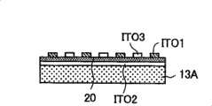
另外,透明基板100A具有玻璃基板10A,在玻璃基板10A的液晶层LC一侧,从玻璃基板10A向液晶层LC依次形成绝缘膜12、层间绝缘膜13A、作为对置电极发挥作用的透明电极ITO2、涂敷型绝缘膜20、像素电极ITO1、以及定向膜15A。进而,在透明基板100A的外侧形成偏光板11A。In addition, the
另外,绝缘膜12由底膜12A、栅极绝缘膜12B、层间绝缘膜12C、以及层间绝缘膜12D构成。In addition, the insulating
返回到图1,D是图像线(也称作漏极线、源极线),G是扫描线(也称作栅极线),SH1~SH4是通孔(也称作接触孔(contact holes)),1是反射电极,2是栅极电极,3是半导体层,4是源极电极(将图像线D称作源极线时,也称作漏极电极)。Returning to Figure 1, D is an image line (also called a drain line, a source line), G is a scanning line (also called a gate line), and SH1-SH4 are through holes (also called contact holes). )), 1 is a reflective electrode, 2 is a gate electrode, 3 is a semiconductor layer, and 4 is a source electrode (when the image line D is called a source line, it is also called a drain electrode).
在此,反射电极1例如是下层钼(Mo)1a和上层铝(Al)1b的两层结构。Here, the
图3是表示图1的等效电路的图,图3的电容元件CLC是液晶电容,电容元件Cst是由夹着涂敷型绝缘膜20形成的像素电极ITO1、和作为对置电极发挥作用的透明电极ITO2形成的保持电容(也称作存储电容)。Fig. 3 is the figure showing the equivalent circuit of Fig. 1, and the capacitive element C LC of Fig. 3 is a liquid crystal capacitor, and the capacitive element C st is formed by the pixel electrode ITO1 that sandwiches the coating
在实际的液晶显示板中,如果图1所示的等效电路例如是使用于移动电话的彩色显示的液晶显示板,就配置成子像素数为240×320×3的矩阵状。本实施例的液晶显示装置的驱动方法,与IPS方式的液晶显示装置的驱动方法相同,所以,省略驱动方法的说明。In an actual liquid crystal display panel, if the equivalent circuit shown in FIG. 1 is a liquid crystal display panel used for color display in a mobile phone, for example, the number of sub-pixels is arranged in a matrix of 240×320×3. The driving method of the liquid crystal display device of this embodiment is the same as the driving method of the IPS type liquid crystal display device, and therefore description of the driving method will be omitted.
本实施例的液晶显示板是半透射型的液晶显示板,形成反射电极1的区域构成反射型液晶显示板,除此之外的部分构成透射型液晶显示板。The liquid crystal display panel of this embodiment is a transflective liquid crystal display panel, the region where the
以下,对图1所示的薄膜晶体管的部分结构进行说明。Hereinafter, a partial structure of the thin film transistor shown in FIG. 1 will be described.
图4是表示沿着图1所示的B-B’切割线的透明基板100A一侧的剖面结构的剖面图。在图4、以及后述的图5A~图5C、图6A~图6B、图7、图9、图13、图14中,省略偏向板11A的图示。Fig. 4 is a cross-sectional view showing a cross-sectional structure of the
如图4所示,在形成于玻璃基板10A的、例如由SiN和SiO2的层压膜构成的底膜12A上,形成半导体层3。半导体层3由非晶硅膜或多晶硅膜构成。As shown in FIG. 4 , the
在该半导体膜3上,形成例如由SiO2构成的栅极绝缘膜12B,在该栅极绝缘膜12B上,形成栅极电极2。On this
在栅极电极2上,形成例如由SiO2和SiN等构成的层间绝缘膜12C,在该层间绝缘膜12C上,形成图像线D和源极电极4。并且,半导体层3经由通孔SH1连接在图像线D上,进而,经由通孔SH2连接在源极电极4。On the
另外,在图像线D和源极电极4上,形成由SiO2和SiN等构成的层间绝缘膜12D,在该层间绝缘膜12D上,形成例如由丙稀树脂等构成的层间绝缘膜13A。In addition, on the image line D and the
在此,在源极电极4上,通孔SH3形成在层间绝缘膜12D和层间绝缘膜13A上。Here, on
在本实施例中,该通孔SH3内也形成有涂敷型绝缘膜20。在此,在通孔SH3内所形成的涂敷型绝缘膜20上形成通孔SH4,通过该通孔SH4内所形成的透明导电膜(例如,ITO:Indium-Tin-Oxide)将像素电极ITO1电连接在源极电极4上。In this embodiment, the coating
这样,像素电极ITO1与像素所形成的有源元件电连接。并且,经由用扫描线G驱动的有源元件,将图像信号从图像线D写入到像素电极ITO1。In this way, the pixel electrode ITO1 is electrically connected to the active element formed by the pixel. And, an image signal is written from the image line D to the pixel electrode ITO1 via the active element driven by the scanning line G. FIG.
以下,对图4所示的涂敷型绝缘膜20的形成方法进行说明。Hereinafter, a method of forming the
图5A~图5C是用于说明图4所示的涂敷型绝缘膜的形成方法的一例的图。5A to 5C are views for explaining an example of a method of forming the coating-type insulating film shown in FIG. 4 .
首先,如图5A所示,利用通常的方法,在玻璃基板10A上形成底膜12A、半导体膜3、栅极绝缘膜12B、栅极电极2、层间绝缘膜12C、图像线D、源极电极4、层间绝缘膜12D、以及层间绝缘膜13A,在源极电极4上,通孔SH3形成在层间绝缘膜12D和层间绝缘膜13A上。进而,形成作为对置电极发挥作用的透明电极ITO2和反射电极1。并且,使涂敷型绝缘材料20a形成厚度例如为2~5μm的膜。层间绝缘膜13A,形成膜厚例如为1.5~3μm的厚度。First, as shown in FIG. 5A, a
接着,如图5B所示,使涂敷型材料20a薄膜化,使得成为例如100~500nm的厚度的膜厚。Next, as shown in FIG. 5B , the coating-
作为进行该薄膜化的方法,在涂敷型绝缘材料20a为感光性材料时,可以不曝光地进行显影,或利用抛光(ashing)使厚度变薄;另外,在涂敷型绝缘材料20a为非感光性材料时,可以利用蚀刻(etching)来进行。As a method of thinning the coating
接着,如图5C所示,形成通孔SH4,形成涂敷型绝缘膜20。Next, as shown in FIG. 5C , via holes SH4 are formed, and a coating
该通孔SH4,在涂敷型绝缘材料20a为感光性材料时,能够通过曝光/显影形成;另外,涂敷型绝缘材料20a为非感光性材料时,用光刻来进行即可。The through hole SH4 can be formed by exposure/development when the
图6A~图6B是用于说明图4所示的涂敷型绝缘膜20的形成方法的其他例子的图。6A to 6B are diagrams for explaining other examples of the formation method of the coating
首先,如图6A所示,利用通常的方法,在玻璃基板10A上形成底膜12A、半导体膜3、栅极绝缘膜12B、栅极电极2、层间绝缘膜12C、图像线D、源极电极4、层间绝缘膜12D、以及层间绝缘膜13A,在源极电极4上,层间绝缘膜12D和层间绝缘膜13A上形成通孔SH3。进而,形成作为对置电极发挥作用的透明电极ITO2和反射电极1。并且,使感光性的涂敷型绝缘材料20a形成厚度例如为2~5μm的厚度的膜。First, as shown in FIG. 6A, a
其次,如图6B所示,利用半曝光技术,通孔SH4的部分(图6B中箭头A的部分)充分曝光,其他部分(图6B中箭头B的部分)半曝光。然后,进行显影,以厚度例如为100~500nm,形成具有通孔SH4的涂敷型绝缘膜20。Secondly, as shown in FIG. 6B , using the half-exposure technique, the part of the through hole SH4 (the part indicated by the arrow A in FIG. 6B ) is fully exposed, and the other part (the part indicated by the arrow B in FIG. 6B ) is half-exposed. Then, development is performed to form a coating-
作为感光性的涂敷型绝缘材料20a,在不曝光地进行显影时,在使用膜厚的膜减少量(膜厚变薄的量)大的情况下,在图6B中,也可以代替半曝光技术而以通常的曝光来显影。As the photosensitive coating-
图7是表示本实施例的液晶显示板的变形例的透明基板100A一侧的剖面结构的剖面图。该图7是表示相当于图1所示的B-B’切割线的部分的剖面结构的剖面图。FIG. 7 is a cross-sectional view showing a cross-sectional structure of a
图7所示的结构,在作为对置电极发挥作用的透明基板100A和反射电极1上,利用CVD法形成绝缘膜23,在其上面形成涂敷型绝缘膜20。In the structure shown in FIG. 7, an insulating
也可以使绝缘膜23形成在涂敷型绝缘膜20和像素电极ITO1之间。The insulating
图13是表示作为涂敷型绝缘膜20的形成方法采用薄薄地涂敷形成涂敷型绝缘材料的情况的图。在作为涂敷型绝缘膜20的形成方法采用薄薄地涂敷形成涂敷型绝缘材料的情况下,如图13A所示,在通孔SH4的区域中,涂敷型绝缘膜20的膜厚变薄,作为对置电极发挥作用的透明电极ITO2和像素电极ITO1有可能发生短路。这样,在薄薄地涂敷形成涂敷型绝缘材料时,在通孔SH4的周围,有可能成为涂敷型绝缘膜20的表面未充分平坦化的状态。为了避免短路问题,只要在通孔SH4的周围不形成对置电极即可。但是,此时存在用于显示的面积减小、开口率降低的问题。另外,存在保持电容减小的问题。FIG. 13 is a diagram showing a case where a coating-type insulating material is formed by thin coating as a method of forming the coating-
对此,在本实施例中,如图4的A所示,在通孔SH4的区域,涂敷型绝缘膜20的膜厚足够厚,因此,表面平坦,覆盖(coverage)良好,作为对置电极发挥作用的透明电极ITO2和像素电极ITO1不会短路。因此,在通孔SH4的附近也可以形成对置电极。On the other hand, in this embodiment, as shown in A of FIG. 4 , in the region of the via hole SH4, the film thickness of the coating
层间绝缘膜13A、涂敷型绝缘材料20a、和涂敷型绝缘膜20的膜厚仅为一例,因此,不限定于例示的范围。当层间绝缘膜13A的膜厚为涂敷型绝缘膜20的膜厚的2倍以上时,如以图13说明的那样,仅薄薄地涂敷涂敷型绝缘材料20a,有可能在台阶部的周围不够平坦,因此,优选的是,通过如图5A~图5C、图6A~图6B所示的工序(process)来形成。The film thicknesses of the
图14是表示在作为对置电极发挥作用的透明电极ITO2和反射电极1上形成由CVD法形成的绝缘膜并使得对置电极和像素电极ITO1之间绝缘的情况的图。FIG. 14 is a diagram showing a state in which an insulating film formed by CVD is formed on the transparent electrode ITO2 functioning as a counter electrode and the
此时,如图14的A所示,不能使由反射电极1引起的凹凸平坦化,因此发生摩擦不充分而产生畴,对比度降低。In this case, as shown in A of FIG. 14 , the unevenness caused by the
但在本实施例中,如图4的B所示,能够吸收反射电极1的台阶,能够使涂敷型绝缘膜20的表面平坦化。由此,能够防止由摩擦不充分产生的畴,能够使对比度提高。However, in this embodiment, as shown in B of FIG. 4 , the level difference of the
在上述专利文献1中,公开了具有平坦化膜210的液晶显示板。但是,在该专利文献中,未公开用涂敷型绝缘膜20来形成保持电容的情况。In the
在本实施例中,像素电极ITO1也可以是如图8所示的、内部具有闭合形状的狭缝30的矩形形状,以取代如图1所示的、具有一部分敞开的形状的狭缝(slit)的梳齿状。无论图1、图8哪种情况,像素电极都是具有线状部分结构。In this embodiment, the pixel electrode ITO1 may also be a rectangular shape with a closed slit 30 inside as shown in FIG. 8 instead of a partially open slit as shown in FIG. 1 . ) in the shape of a comb. No matter which case is shown in FIG. 1 and FIG. 8 , the pixel electrode has a linear partial structure.
图9是表示本实施例的液晶显示板的变形例的透明基板100A一侧的剖面结构的剖面图。该图9是表示相当于B-B’切割线的部分的剖面结构的剖面图。FIG. 9 is a cross-sectional view showing a cross-sectional structure of a
在图9所示的结构中,为了使入射到反射电极1的光进行散射/反射,在反射电极1上形成了凹凸。在这种结构中,也能够消除反射电极1的凹凸,使涂敷型绝缘膜20的表面平坦化。In the structure shown in FIG. 9 , in order to scatter/reflect light incident on the
在图9所示的结构中,省略了对置电极的图示,但在通常的IPS方式的液晶显示板的情况下,形成在透明基板100A一侧,另外,在纵向电场方式(例如TN方式、VA方式等)的液晶显示板的情况下,形成在透明基板100B一侧。另外,在IPS方式的情况下,反射电极1也可以兼作对置电极。In the structure shown in FIG. 9 , the illustration of the counter electrode is omitted, but in the case of a general IPS liquid crystal display panel, it is formed on the
这样,本发明不限定于使用平面状的对置电极的IPS方式的液晶显示板,也可应用于通常IPS方式的液晶显示板或纵向电场方向的液晶显示板。Thus, the present invention is not limited to an IPS liquid crystal display panel using planar counter electrodes, but can also be applied to a normal IPS liquid crystal display panel or a vertical electric field direction liquid crystal display panel.
此时,透明电极ITO2或反射电极1,在与像素电极ITO1之间被用作用于形成保持电容Cst的电极。At this time, the transparent electrode ITO2 or the
在纵向电场方式的液晶显示板的情况下,像素电极ITO1也可以是不具有狭缝的形状,为了使其多畴化,也可以形成狭缝。In the case of a vertical electric field type liquid crystal display panel, the pixel electrode ITO1 may not have a slit shape, or may be formed with slits in order to achieve multi-domain.
图10是表示本发明的实施例的液晶显示板的变形例的一子像素的结构的平面图。10 is a plan view showing the structure of one sub-pixel in a modified example of the liquid crystal display panel according to the embodiment of the present invention.
图11是表示沿着图10所示的A-A’切割线的剖面结构的剖面图。Fig. 11 is a cross-sectional view showing a cross-sectional structure along the cutting line A-A' shown in Fig. 10 .
图10、图11所示的结构是将本发明应用于通常的IPS方式的液晶显示板的情况的结构。The structures shown in FIGS. 10 and 11 are structures in which the present invention is applied to a general IPS type liquid crystal display panel.
在图10、图11中,ITO3表示对置电极。在图11中,透明电极ITO2的下层一侧(玻璃基板10A一侧),省略了层间绝缘膜13A以外的结构的图示。在图10中,透明电极ITO2,也发挥对置电极的作用和形成保持电容的作用。In FIGS. 10 and 11 , ITO3 represents a counter electrode. In FIG. 11 , illustration of structures other than the interlayer insulating
图12是表示本发明的实施例的液晶显示板的变形例的结构的剖面图。该图12是表示相当于图1所示的A-A’切割线的部分的剖面结构的剖面图。12 is a cross-sectional view showing the structure of a modified example of the liquid crystal display panel of the embodiment of the present invention. This FIG. 12 is a cross-sectional view showing a cross-sectional structure of a portion corresponding to the cutting line A-A' shown in FIG. 1 .
图12所示的结构是将本发明应用于纵向电场的液晶显示板的情况的结构。The structure shown in FIG. 12 is a structure in the case of applying the present invention to a liquid crystal display panel in a longitudinal electric field.
在纵向电场的液晶显示板中,对置电极(也称作公共电极)ITO3形成在透明基板100B一侧。另外,透明电极ITO2发挥形成保持电容的作用。也可以与图9的实施例进行组合形成反射电极1。In the longitudinal electric field liquid crystal display panel, the counter electrode (also referred to as a common electrode) ITO3 is formed on the side of the
以上,基于上述实施例,具体说明了由本发明人完成的发明,但本发明不限于上述实施例,当然,在不超出其主旨的范围内可进行各种变更。As mentioned above, the invention made by this inventor was concretely demonstrated based on the said Example, However, this invention is not limited to the said Example, Of course, various changes are possible in the range which does not deviate from the summary.
例如,也可以应用于不是半透射型、而是透射型或反射型的液晶显示装置。在透射型的情况下,可省略反射电极1。在反射型的情况下,只要形成反射电极1即可,以取代透明电极ITO2。For example, it can also be applied to a transmissive or reflective liquid crystal display device instead of a transflective type. In the case of the transmissive type, the
在透射型或半透射型的情况下,也可以在液晶显示板的背面配置未图示的背光源。在反射型的情况下,也可以在液晶显示板的前面(观察者一侧)配置未图示的前光源。In the case of a transmissive type or a semi-transmissive type, a backlight (not shown) may be arranged on the back of the liquid crystal display panel. In the case of the reflective type, a front light source (not shown) may be arranged on the front side (observer side) of the liquid crystal display panel.
另外,本发明不限于液晶显示装置,也可应用于具有有源元件和保持电容的显示装置。In addition, the present invention is not limited to liquid crystal display devices, but can also be applied to display devices having active elements and storage capacitors.
Claims (10)
Applications Claiming Priority (2)
| Application Number | Priority Date | Filing Date | Title |
|---|---|---|---|
| JP2005312165A JP5258156B2 (en) | 2005-10-27 | 2005-10-27 | Liquid crystal display device and manufacturing method thereof |
| JP312165/2005 | 2005-10-27 |
Publications (2)
| Publication Number | Publication Date |
|---|---|
| CN1955803A CN1955803A (en) | 2007-05-02 |
| CN100478755C true CN100478755C (en) | 2009-04-15 |
Family
ID=37995789
Family Applications (1)
| Application Number | Title | Priority Date | Filing Date |
|---|---|---|---|
| CNB2006101427103A Active CN100478755C (en) | 2005-10-27 | 2006-10-26 | Liquid crystal display device |
Country Status (5)
| Country | Link |
|---|---|
| US (1) | US7639331B2 (en) |
| JP (1) | JP5258156B2 (en) |
| KR (1) | KR100880969B1 (en) |
| CN (1) | CN100478755C (en) |
| TW (1) | TWI357529B (en) |
Families Citing this family (24)
| Publication number | Priority date | Publication date | Assignee | Title |
|---|---|---|---|---|
| JP5170985B2 (en) | 2006-06-09 | 2013-03-27 | 株式会社ジャパンディスプレイイースト | Liquid crystal display |
| JP4818839B2 (en) * | 2006-07-19 | 2011-11-16 | 株式会社 日立ディスプレイズ | Liquid crystal display device and manufacturing method thereof |
| JP2009020232A (en) * | 2007-07-11 | 2009-01-29 | Hitachi Displays Ltd | Liquid crystal display |
| US8218116B2 (en) | 2007-08-01 | 2012-07-10 | Sony Corporation | Liquid crystal display panel and manufacturing method thereof |
| JP2009042292A (en) | 2007-08-06 | 2009-02-26 | Hitachi Displays Ltd | Liquid crystal display apparatus |
| JP5235363B2 (en) * | 2007-09-04 | 2013-07-10 | 株式会社ジャパンディスプレイイースト | Liquid crystal display |
| JP5215617B2 (en) * | 2007-09-04 | 2013-06-19 | 株式会社ジャパンディスプレイイースト | Liquid crystal display |
| JP5075583B2 (en) | 2007-11-01 | 2012-11-21 | 株式会社ジャパンディスプレイイースト | Liquid crystal display |
| JP5079462B2 (en) * | 2007-11-19 | 2012-11-21 | 株式会社ジャパンディスプレイウェスト | Liquid crystal device and electronic device |
| JP5352333B2 (en) * | 2009-04-23 | 2013-11-27 | 株式会社ジャパンディスプレイ | Active matrix display device |
| US8633481B2 (en) * | 2010-08-30 | 2014-01-21 | Sharp Kabushiki Kaisha | Semiconductor device and process for production thereof |
| US9239501B2 (en) | 2012-07-26 | 2016-01-19 | Innocom Technology(Shenzhen) Co., Ltd. | Liquid crystal display device |
| CN103869508B (en) * | 2012-12-13 | 2016-08-31 | 京东方科技集团股份有限公司 | Weld pad of array base palte and preparation method thereof and array base palte and liquid crystal indicator |
| CN103984175B (en) * | 2013-02-08 | 2017-03-01 | 瀚宇彩晶股份有限公司 | Semi-transmissive semi-reflective liquid crystal display and manufacturing method thereof |
| KR20150021408A (en) * | 2013-08-20 | 2015-03-02 | 삼성디스플레이 주식회사 | Thin film transistor substrate, fabrication method of the same, and display apparatus |
| TWI511303B (en) * | 2013-08-30 | 2015-12-01 | Ye Xin Technology Consulting Co Ltd | Array substrate of liquid crystal display |
| JP6242121B2 (en) * | 2013-09-02 | 2017-12-06 | 株式会社ジャパンディスプレイ | LIGHT EMITTING DEVICE DISPLAY DEVICE AND LIGHT EMITTING DEVICE DISPLAY DEVICE MANUFACTURING METHOD |
| US9530801B2 (en) * | 2014-01-13 | 2016-12-27 | Apple Inc. | Display circuitry with improved transmittance and reduced coupling capacitance |
| JP2015145907A (en) * | 2014-01-31 | 2015-08-13 | 株式会社ジャパンディスプレイ | Manufacturing method of display device |
| JP2016085308A (en) * | 2014-10-24 | 2016-05-19 | 株式会社ジャパンディスプレイ | Liquid crystal display device and substrate for display device |
| KR102372774B1 (en) * | 2015-03-26 | 2022-03-11 | 삼성디스플레이 주식회사 | Organic light emitting diode display |
| JP6412036B2 (en) * | 2015-12-21 | 2018-10-24 | 株式会社ジャパンディスプレイ | Display device |
| JP6139730B2 (en) * | 2016-03-18 | 2017-05-31 | 株式会社ジャパンディスプレイ | Display device and manufacturing method thereof |
| US10330991B1 (en) * | 2018-05-31 | 2019-06-25 | a.u. Vista Inc. | Liquid crystal display devices with electrode stacks and methods for manufacturing such devices |
Family Cites Families (13)
| Publication number | Priority date | Publication date | Assignee | Title |
|---|---|---|---|---|
| DE69332142T2 (en) * | 1992-12-25 | 2003-03-06 | Sony Corp., Tokio/Tokyo | Active matrix substrate |
| JP3383047B2 (en) | 1992-12-25 | 2003-03-04 | ソニー株式会社 | Active matrix substrate |
| KR100299381B1 (en) * | 1998-08-24 | 2002-06-20 | 박종섭 | Liquid crystal display device having high opening ratio and high transmittance and manufacturing method thereof |
| JP4454713B2 (en) | 1999-03-17 | 2010-04-21 | 株式会社半導体エネルギー研究所 | Semiconductor device and manufacturing method thereof |
| KR100565887B1 (en) * | 1999-06-11 | 2006-03-31 | 마쯔시다덴기산교 가부시키가이샤 | LCD and its manufacturing method |
| JP2001154220A (en) | 1999-11-24 | 2001-06-08 | Sharp Corp | Active matrix substrate and liquid crystal display device using the same |
| TW513600B (en) * | 2000-06-07 | 2002-12-11 | Ind Tech Res Inst | In-plane switching liquid crystal displaying device and method of fabricating the same |
| JP4722319B2 (en) * | 2001-04-26 | 2011-07-13 | 株式会社日立製作所 | Liquid crystal display |
| KR100757786B1 (en) * | 2001-07-27 | 2007-09-11 | 삼성전자주식회사 | Reflective-transmissive liquid crystal display device and manufacturing method thereof |
| KR100820647B1 (en) * | 2001-10-29 | 2008-04-08 | 엘지.필립스 엘시디 주식회사 | Array board for transflective liquid crystal display device and manufacturing method thereof |
| JP4419414B2 (en) * | 2003-03-27 | 2010-02-24 | セイコーエプソン株式会社 | Transflective liquid crystal display device |
| KR100524621B1 (en) * | 2003-05-23 | 2005-10-28 | 엘지.필립스 엘시디 주식회사 | Transflective liquid crystal display device and fabrication method of the same |
| KR100604192B1 (en) * | 2003-12-30 | 2006-07-25 | 엘지.필립스 엘시디 주식회사 | Array board for transverse electric field type liquid crystal display device and manufacturing method thereof |
-
2005
- 2005-10-27 JP JP2005312165A patent/JP5258156B2/en active Active
-
2006
- 2006-10-26 KR KR1020060104242A patent/KR100880969B1/en active IP Right Grant
- 2006-10-26 US US11/586,541 patent/US7639331B2/en active Active
- 2006-10-26 CN CNB2006101427103A patent/CN100478755C/en active Active
- 2006-10-27 TW TW095139879A patent/TWI357529B/en active
Also Published As
| Publication number | Publication date |
|---|---|
| US7639331B2 (en) | 2009-12-29 |
| KR20070045936A (en) | 2007-05-02 |
| TWI357529B (en) | 2012-02-01 |
| US20070097303A1 (en) | 2007-05-03 |
| JP2007121587A (en) | 2007-05-17 |
| KR100880969B1 (en) | 2009-02-03 |
| JP5258156B2 (en) | 2013-08-07 |
| TW200732803A (en) | 2007-09-01 |
| CN1955803A (en) | 2007-05-02 |
Similar Documents
| Publication | Publication Date | Title |
|---|---|---|
| CN100478755C (en) | Liquid crystal display device | |
| CN100443968C (en) | Liquid crystal device and electronic equipment | |
| JP5057324B2 (en) | Liquid crystal device and electronic device | |
| CN101441371A (en) | Liquid crystal device and electronic apparatus | |
| JP2009109821A (en) | Optical element, liquid crystal device and electronic apparatus | |
| JP2003344836A (en) | Transflective liquid crystal device and electronic device using the same | |
| JP5919636B2 (en) | Electro-optical device, electronic apparatus, and method of manufacturing electro-optical device | |
| JP2008111903A (en) | Liquid crystal device and electronic device | |
| JP2004020907A (en) | Liquid crystal display device | |
| JP5948777B2 (en) | Liquid crystal device, method for manufacturing liquid crystal device, and electronic apparatus | |
| JP4764871B2 (en) | Transflective liquid crystal display panel and manufacturing method thereof | |
| JP3763285B2 (en) | Liquid crystal display | |
| JP2003075851A (en) | Liquid crystal display device, method of manufacturing the same, and electronic device | |
| JP2002182238A (en) | Electro-optical device and method of manufacturing the same, substrate device and method of manufacturing the same | |
| KR101603224B1 (en) | Thin film transistor substrate of transflective liquid crystal display and method for fabricating the same | |
| JP4400027B2 (en) | Transflective / reflective electro-optical device and electronic apparatus using the same | |
| JP2008157997A (en) | Liquid crystal device and electronic device | |
| JP5483637B2 (en) | Manufacturing method of liquid crystal display device | |
| JP4858081B2 (en) | Electro-optical device and manufacturing method thereof | |
| JP2002341380A (en) | Electro-optical device and electronic equipment including the same | |
| JP2007219053A (en) | Liquid crystal device and electronic appliance | |
| JP2003195285A (en) | Reflective electro-optical device, electronic apparatus, and method of manufacturing reflective electro-optical device | |
| JP2004045756A (en) | Transflective / reflective electro-optical device and electronic apparatus using the same | |
| JP2024169040A (en) | Electro-optical devices and electronic equipment | |
| JP2015200766A (en) | Microlens array substrate, method for manufacturing microlens array substrate, liquid crystal device, electronic device |
Legal Events
| Date | Code | Title | Description |
|---|---|---|---|
| C06 | Publication | ||
| PB01 | Publication | ||
| C10 | Entry into substantive examination | ||
| SE01 | Entry into force of request for substantive examination | ||
| C14 | Grant of patent or utility model | ||
| GR01 | Patent grant | ||
| C56 | Change in the name or address of the patentee | ||
| CP01 | Change in the name or title of a patent holder |
Address after: Chiba County, Japan Co-patentee after: Panasonic Liquid Crystal Display Co.,Ltd. Patentee after: Hitachi Displays, Ltd. Address before: Chiba County, Japan Co-patentee before: IPS pioneer support society Patentee before: Hitachi Displays, Ltd. Address after: Chiba County, Japan Co-patentee after: IPS Pioneer Support Society Patentee after: Hitachi Displays, Ltd. Address before: Chiba County, Japan Patentee before: Hitachi Displays, Ltd. |
|
| C56 | Change in the name or address of the patentee |
Owner name: JAPAN DISPLAY, INC. Free format text: FORMER NAME: APAN DISPLAY EAST, INC. Owner name: APAN DISPLAY EAST, INC. Free format text: FORMER NAME: HITACHI DISPLAY CO., LTD. |
|
| CP01 | Change in the name or title of a patent holder |
Address after: Chiba County, Japan Patentee after: Japan Display East Inc. Patentee after: Panasonic Liquid Crystal Display Co.,Ltd. Address before: Chiba County, Japan Patentee before: Hitachi Displays, Ltd. Patentee before: Panasonic Liquid Crystal Display Co.,Ltd. |
|
| CP03 | Change of name, title or address |
Address after: Tokyo port xixinqiao Japan three chome 7 No. 1 Patentee after: JAPAN DISPLAY Inc. Patentee after: Panasonic Liquid Crystal Display Co.,Ltd. Address before: Chiba County, Japan Patentee before: Japan Display East Inc. Patentee before: Panasonic Liquid Crystal Display Co.,Ltd. |
|
| EE01 | Entry into force of recordation of patent licensing contract |
Application publication date: 20070502 Assignee: BOE TECHNOLOGY GROUP Co.,Ltd. Assignor: JAPAN DISPLAY Inc.|Panasonic Liquid Crystal Display Co.,Ltd. Contract record no.: 2013990000688 Denomination of invention: Liquid crystal display device Granted publication date: 20090415 License type: Common License Record date: 20131016 |
|
| LICC | Enforcement, change and cancellation of record of contracts on the licence for exploitation of a patent or utility model | ||
| TR01 | Transfer of patent right |
Effective date of registration: 20231213 Address after: Tokyo, Japan Patentee after: JAPAN DISPLAY Inc. Patentee after: PANASONIC INTELLECTUAL PROPERTY CORPORATION OF AMERICA Address before: Tokyo port xixinqiao Japan three chome 7 No. 1 Patentee before: JAPAN DISPLAY Inc. Patentee before: Panasonic Liquid Crystal Display Co.,Ltd. |
|
| TR01 | Transfer of patent right |