CN100477021C - Techniques for fabricating a resistor on a flexible base material - Google Patents
Techniques for fabricating a resistor on a flexible base material Download PDFInfo
- Publication number
- CN100477021C CN100477021C CNB038250748A CN03825074A CN100477021C CN 100477021 C CN100477021 C CN 100477021C CN B038250748 A CNB038250748 A CN B038250748A CN 03825074 A CN03825074 A CN 03825074A CN 100477021 C CN100477021 C CN 100477021C
- Authority
- CN
- China
- Prior art keywords
- layer
- flexible substrate
- semiconductor device
- resistor
- activating area
- Prior art date
- Legal status (The legal status is an assumption and is not a legal conclusion. Google has not performed a legal analysis and makes no representation as to the accuracy of the status listed.)
- Expired - Fee Related
Links
Images


Classifications
-
- H—ELECTRICITY
- H01—ELECTRIC ELEMENTS
- H01C—RESISTORS
- H01C3/00—Non-adjustable metal resistors made of wire or ribbon, e.g. coiled, woven or formed as grids
- H01C3/06—Flexible or folding resistors, whereby such a resistor can be looped or collapsed upon itself
-
- H—ELECTRICITY
- H01—ELECTRIC ELEMENTS
- H01C—RESISTORS
- H01C17/00—Apparatus or processes specially adapted for manufacturing resistors
- H01C17/06—Apparatus or processes specially adapted for manufacturing resistors adapted for coating resistive material on a base
- H01C17/075—Apparatus or processes specially adapted for manufacturing resistors adapted for coating resistive material on a base by thin film techniques
- H01C17/12—Apparatus or processes specially adapted for manufacturing resistors adapted for coating resistive material on a base by thin film techniques by sputtering
-
- B—PERFORMING OPERATIONS; TRANSPORTING
- B29—WORKING OF PLASTICS; WORKING OF SUBSTANCES IN A PLASTIC STATE IN GENERAL
- B29C—SHAPING OR JOINING OF PLASTICS; SHAPING OF MATERIAL IN A PLASTIC STATE, NOT OTHERWISE PROVIDED FOR; AFTER-TREATMENT OF THE SHAPED PRODUCTS, e.g. REPAIRING
- B29C59/00—Surface shaping of articles, e.g. embossing; Apparatus therefor
- B29C59/14—Surface shaping of articles, e.g. embossing; Apparatus therefor by plasma treatment
-
- H—ELECTRICITY
- H01—ELECTRIC ELEMENTS
- H01C—RESISTORS
- H01C7/00—Non-adjustable resistors formed as one or more layers or coatings; Non-adjustable resistors made from powdered conducting material or powdered semi-conducting material with or without insulating material
- H01C7/006—Thin film resistors
-
- H—ELECTRICITY
- H05—ELECTRIC TECHNIQUES NOT OTHERWISE PROVIDED FOR
- H05K—PRINTED CIRCUITS; CASINGS OR CONSTRUCTIONAL DETAILS OF ELECTRIC APPARATUS; MANUFACTURE OF ASSEMBLAGES OF ELECTRICAL COMPONENTS
- H05K1/00—Printed circuits
- H05K1/16—Printed circuits incorporating printed electric components, e.g. printed resistor, capacitor, inductor
- H05K1/167—Printed circuits incorporating printed electric components, e.g. printed resistor, capacitor, inductor incorporating printed resistors
-
- H—ELECTRICITY
- H05—ELECTRIC TECHNIQUES NOT OTHERWISE PROVIDED FOR
- H05K—PRINTED CIRCUITS; CASINGS OR CONSTRUCTIONAL DETAILS OF ELECTRIC APPARATUS; MANUFACTURE OF ASSEMBLAGES OF ELECTRICAL COMPONENTS
- H05K1/00—Printed circuits
- H05K1/02—Details
- H05K1/03—Use of materials for the substrate
- H05K1/0313—Organic insulating material
- H05K1/032—Organic insulating material consisting of one material
- H05K1/0346—Organic insulating material consisting of one material containing N
-
- H—ELECTRICITY
- H05—ELECTRIC TECHNIQUES NOT OTHERWISE PROVIDED FOR
- H05K—PRINTED CIRCUITS; CASINGS OR CONSTRUCTIONAL DETAILS OF ELECTRIC APPARATUS; MANUFACTURE OF ASSEMBLAGES OF ELECTRICAL COMPONENTS
- H05K2201/00—Indexing scheme relating to printed circuits covered by H05K1/00
- H05K2201/01—Dielectrics
- H05K2201/0137—Materials
- H05K2201/0154—Polyimide
-
- H—ELECTRICITY
- H05—ELECTRIC TECHNIQUES NOT OTHERWISE PROVIDED FOR
- H05K—PRINTED CIRCUITS; CASINGS OR CONSTRUCTIONAL DETAILS OF ELECTRIC APPARATUS; MANUFACTURE OF ASSEMBLAGES OF ELECTRICAL COMPONENTS
- H05K2201/00—Indexing scheme relating to printed circuits covered by H05K1/00
- H05K2201/03—Conductive materials
- H05K2201/0302—Properties and characteristics in general
- H05K2201/0317—Thin film conductor layer; Thin film passive component
-
- H—ELECTRICITY
- H05—ELECTRIC TECHNIQUES NOT OTHERWISE PROVIDED FOR
- H05K—PRINTED CIRCUITS; CASINGS OR CONSTRUCTIONAL DETAILS OF ELECTRIC APPARATUS; MANUFACTURE OF ASSEMBLAGES OF ELECTRICAL COMPONENTS
- H05K2203/00—Indexing scheme relating to apparatus or processes for manufacturing printed circuits covered by H05K3/00
- H05K2203/09—Treatments involving charged particles
- H05K2203/095—Plasma, e.g. for treating a substrate to improve adhesion with a conductor or for cleaning holes
-
- H—ELECTRICITY
- H05—ELECTRIC TECHNIQUES NOT OTHERWISE PROVIDED FOR
- H05K—PRINTED CIRCUITS; CASINGS OR CONSTRUCTIONAL DETAILS OF ELECTRIC APPARATUS; MANUFACTURE OF ASSEMBLAGES OF ELECTRICAL COMPONENTS
- H05K2203/00—Indexing scheme relating to apparatus or processes for manufacturing printed circuits covered by H05K3/00
- H05K2203/11—Treatments characterised by their effect, e.g. heating, cooling, roughening
- H05K2203/1136—Conversion of insulating material into conductive material, e.g. by pyrolysis
-
- H—ELECTRICITY
- H05—ELECTRIC TECHNIQUES NOT OTHERWISE PROVIDED FOR
- H05K—PRINTED CIRCUITS; CASINGS OR CONSTRUCTIONAL DETAILS OF ELECTRIC APPARATUS; MANUFACTURE OF ASSEMBLAGES OF ELECTRICAL COMPONENTS
- H05K3/00—Apparatus or processes for manufacturing printed circuits
- H05K3/38—Improvement of the adhesion between the insulating substrate and the metal
- H05K3/381—Improvement of the adhesion between the insulating substrate and the metal by special treatment of the substrate
-
- H—ELECTRICITY
- H05—ELECTRIC TECHNIQUES NOT OTHERWISE PROVIDED FOR
- H05K—PRINTED CIRCUITS; CASINGS OR CONSTRUCTIONAL DETAILS OF ELECTRIC APPARATUS; MANUFACTURE OF ASSEMBLAGES OF ELECTRICAL COMPONENTS
- H05K3/00—Apparatus or processes for manufacturing printed circuits
- H05K3/38—Improvement of the adhesion between the insulating substrate and the metal
- H05K3/388—Improvement of the adhesion between the insulating substrate and the metal by the use of a metallic or inorganic thin film adhesion layer
Landscapes
- Engineering & Computer Science (AREA)
- Microelectronics & Electronic Packaging (AREA)
- Physics & Mathematics (AREA)
- Plasma & Fusion (AREA)
- Electromagnetism (AREA)
- Manufacturing & Machinery (AREA)
- Apparatuses And Processes For Manufacturing Resistors (AREA)
Abstract
A technique for fabricating a resistor on a flexible substrate (10) (28). Specifically, at least a portion of a polyimide substrate (10) (28) is activated by exposure to a ion sputter etch techniques. A metal layer (14) (36) is depositing over the activated portion (12) (34) of the substrate (10) (28), thereby resulting in the formation of a highly resistive metal-carbide region (16) (38). Interconnect layers (18, 20) (40, 42) are deposited over the metal-carbide region (16) (38) and patterned to form terminals (24, 26) (44, 46) at opposite ends of the metal carbide region (l6) (38). The metal-carbide region (16) (38) is patterned to form a resistor between the terminals. Alternatively, only a selected area of the polyimide substrate (10) (28) is activated. The selected area forms the area in which the metal-carbide region (16) (38) is formed. Interconnect layers (18, 20) (40, 42) are disposed over the metal-carbide region (16) (38) and patterned to form terminals (24, 26) (44, 46) at opposite ends of the metal-carbide region (16) (38).
Description
Technical field
The preparation of relate generally to resistor of the present invention, more specifically, high resistance structure that the present invention relates on flexible base material, form and the technology that is used to prepare this structure.
Background technology
Many commerce is used and has been adopted the semiconductor device that is subject to electrostatic discharge effect.A kind of device that semiconductor light-emitting-diode (LED) comes to this.LED is a semiconductor chip, and voltage that its packed response is applied or electric current are with emitted radiation.These LED are used in many commercial application, and are luminous such as automobile, demonstration, safety/emergency and alignment regions.Can use the material of any visible emitting, ultraviolet or infrared radiation to prepare LED.Therefore, the LED device can comprise the material that has the semiconductor layer p-n junction and can launch desirable radiation.For example, the LED device can use any semiconducting compound layer preparation that meets the requirements: III-V semiconducting compound layer, such as GaAs, GaAlAs, GaN, InGaN, GaP etc.; II-VI semiconducting compound layer is such as ZnSe, ZnSSe, CdTe etc.; Or IV-IV semiconducting compound layer, such as SiC.In addition, the LED device also can comprise other layers, such as coating layer, ducting layer and contact layer.
At present, semiconductor device (such as, LED) can prepare on flexible base material (such as, polyimides) the flexible devices array is provided, thereby be used in the various products to adapt with various difformities.For example, led array can prepare on flexible base material to be used for luminous product, such as circular bulb, diffuse luminarie, cylindrical flashlights etc.But, semiconductor device (such as, GaN base LED) for example to the static discharge sensitivity, because their preparations are on the insulation Sapphire Substrate.Therefore, except by the LED, just be not clearly used as the discharge path of static discharge.May produce severe impairment to LED by the LED static discharge, the p-n junction performance of device is reduced.So it will be favourable creating other electrostatic discharging path.
A kind of minimizing semiconductor device (such as, LED) mechanism of static damage possibility is to provide a discharge path for electric-charge-dissipating in conjunction with high value bleeder resistance (bleed resistor).But for the semiconductor device for preparing on flexible base material, preparation resistance may bring some challenge.Usually, be difficult to go up the film resistor of the small-sized high value (scope is 100k ohm-1M ohm) of preparation in flexible base material (such as, polyimides).Normally used resistance film is such as tantalum nitride (TaN
2), the scope of the sheet resistance value of chromaking nickel (NiCr) and chromium silicide (CrSi) is 100-300 ohm-sq rice.For these values, the resistance in 100k ohm-1M ohm scope is generally with the serpentine configuration patterning, and this can cover very large area.For the semiconductor device of preparation on flexible base material, be used for preparing high-resistance thin film resistor large-scale serpentine configuration may and infeasible.In addition, the processing flexible base material (such as, polyimide film) generally need low relatively temperature (<200 ℃), so that this film can keep the globality of structure.Handle the required low temperature of flexible base material and got rid of and use many materials that are used in preparation high resistance measurement in the semiconductor device usually, because these material requires are greater than 200 ℃ treatment temperature.
Summary of the invention
According to an aspect of the present invention, provide a kind of preparation method of resistor, this method comprises the steps: to activate the lip-deep zone of flexible substrate, forms activating area thus; In activating area, form resistive layer; At one or more layers interconnection layer of deposition to the small part resistive layer; And one or more layers interconnection layer of patterning forms the terminal of resistor.
According to another aspect of the present invention, provide a kind of preparation method of resistor, this method comprises the steps: to activate the surface of flexible substrate, forms active layer thus; On the surface of active layer, deposit the first metal layer, form resistive layer thereby in this active layer, produce reaction thus; The one or more interconnection layers of deposition on the first metal layer; Each and the first metal layer etching in one or more interconnection layers up to resistive layer, are formed terminal thus; And resistive layer patternization formed the resistor that is coupled between the terminal.
According to another aspect of the present invention, provide a kind of preparation method of resistor, this method comprises the steps: deposition mas layer on the surface of flexible substrate; In mask layer, form opening, appear the part flexible substrate by opening thus; Activation flexible substrate exposed portions forms activating area thus; Surface removal mask layer from flexible substrate; One or more layers interconnection layer of deposition on the flexible substrate surface; And one or more layers interconnection layer of patterning forms the independently terminal that passes through the mutual electric coupling of activating area mutually.
According to another aspect of the present invention, provide a kind of device, this device comprises: flexible substrate, the resistance region that forms on flexible substrate and have first end and second end, and the conducting terminal that is coupled in first end and second end each.
According to another aspect of the present invention, a kind of device is provided, this device comprises flexible substrate with first side and second side, be coupled to flexible substrate first side and be electrically coupled to flexible substrate second side contact area light-emitting diode (LED) and be formed on resistor on flexible substrate second side, wherein the resistor electric coupling is between each contact area.
Description of drawings
Fig. 1-6A illustrates the viewgraph of cross-section that is used to prepare first exemplary technique of resistor according to of the present invention;
Fig. 7-12A illustrates the viewgraph of cross-section that is used to prepare second exemplary technique of resistor according to of the present invention;
Figure 13 illustrates the cross sectional representation of exemplary light-emitting diode (LED) die array; And
Figure 14 illustrates LED die array shown in Figure 13 and is combined with rear view according to the resistor of present technique.
Embodiment
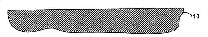
Now, will first exemplary technique that prepare high resistance measurement device (scope is 100k ohm-1M ohm) on flexible base material be described with reference to figure 1-6A.Fig. 1 illustrates and will prepare the flexible substrate material 10 of resistor thereon.Flexible substrate 10 has the thickness of 0.5-3 mil, and comprises the flexiplast sheet that can be bent into intended shape.Can flexible substrate crooked or bending be defined as by the test of standard bending strength method, be no more than 10 at 23 degrees centigrade of following modulus of elasticity, the film of 000PSI or composition.Flexible substrate material 10 is electrical insulating materials, preferably includes the thin polymer film that can adhere to electric conducting material on it.Flexible substrate material 10 is included in modulus of elasticity, thermal coefficient of expansion and the hygral expansion coefficient that makes the change in size minimum during the processing.In order to keep flexible, the thickness of flexible substrate material 10 can minimize.But backing material 10 also has enough rigidity (because thickness or material are formed) and keeps dimensionally stable with the support metal layer and in all subsequently treatment steps.Flexible substrate 10 generally comprises any in the multiple polyimide-based material.For example, flexible substrate material 10 can comprise the Nemours﹠amp by E.I.DuPont De; Co. rolling provides
 Polyimide piece is provided by Kanegafuchi Chem.Indus.Co.
 Polyimide piece, or provide by UBE Indus.Inc.
 Polyimide piece.Although the present technique relate generally to is gone up the preparation resistor in flexible base material (such as, polyimides), exemplary technique described herein also can be implemented on the bigger substrate of the rigidity with polyimide-based top layer.
Beginning, flexible substrate 10 is placed in the vacuum chamber, can implement the physical vapor deposition (PVD) technology therein and activate flexible substrate 10.Surface by activation flexible substrate 10 makes it have more activity, thereby can form carbon bond more easily, as will be described as further below.In order to implement PVD technology, on the substrate carrier in flexible substrate 10 placed cavities, will gas introduction chamber such as argon gas (Ar) in.In order to reduce the pollutant in the chamber and on flexible substrate 10 surfaces, to provide cleaning effect, can apply little back bias voltage (electric charge) to substrate carrier.In conjunction with electrical bias, can use radio frequency (RF) sputter to come advantageously etching and the surface of cleaning flexible substrate 10 exposures.Argon gas (Ar) is imported in the vacuum chamber and ionization is positive charge, by substrate carrier being biased to the field electromotive force different with this argon gas, makes the surface that ar atmo directly clashes into flexible substrate 10 exposures realize etching and cleaning.The depollution thing that gets on from flexible substrate 10 surfaces has improved electrically contacting between flexible substrate 10 zones that expose and the material disposed thereon subsequently, and has improved the adhesiveness to flexible substrate 10 surfaces.
Except removing surface impurity, the ion bombardment on argon (Ar) ion pair flexible substrate 10 surfaces also causes the preferential scission of link of imines carbonyl and forms graphite-like carbon, then " activation " surface of flexible substrate 10 make it can accept to form the carbide bonding thus with the other materials that is imported.Fig. 2 shows the bombardment on argon (Ar) ion pair flexible substrate 10 surfaces.As previously mentioned, surface impurity has been removed in ion bombardment, and has activated the surface of flexible substrate 10.Surface by activation flexible substrate 10 has formed activating area 12 on the surface of flexible substrate 10.As described below, be easy to make up the active region that forms high resistance area by providing with other materials, activating area 12 can be used to form the electric resistance structure of high value.
As shown in Figure 3, after having activated flexible substrate 10, titanium deposition on flexible substrate 10 (Ti) layer 14.This Ti layer 14 can use the PVD technology setting of second type, such as planar magnetic control sputtering.As one of ordinary skill in the understanding, can use low chamber to press and be lower than 200 ℃ cavity temperature and realize magnetron sputtering, these conditions help being prepared on polyimide-based material (such as flexible substrate 10).For example, set Ti layer 14 thickness can be 300 dusts-1000 dust.System such as MRC 603 can be used to realize magnetron sputtering.In one embodiment, the chamber can be set at the pressure of 6 μ and under the power level of 800W, work Ti layer 14 was set in 4 minutes.
When Ti layer 14 was set at flexible substrate 10, the activating area of flexible substrate 10 12 react consumingly with titanium (Ti), the electric charge transfer occurred via the carbonyl of activating area 12.As shown in Figure 3, along with Ti layer 14 coverage rate increase, in the active region 12 of flexible substrate 10, formed thin titanium carbide (Ti-C) layer 16.Ti-C layer 16 is highly ohmic (100k ohm-1M ohm), so can be used in the resistor for preparing high value (100k ohm-1M ohm) on the surface of flexible substrate 10.
As shown in Figure 4, at depositing Ti layer 14 with after forming Ti-C layer 16, can on Ti layer 14, deposit interconnection material.For example, can pass through physical vapor deposition (PVD) technology deposited copper (Cu) inculating crystal layer 18 on Ti layer 14.The thickness of the Cu inculating crystal layer 18 that for example, is deposited can be 3000 dusts.Next, can electroplate Cu inculating crystal layer 18.At last, for example can finish interconnection by PVD technology titanium deposition (Ti) inculating crystal layer 20 on Cu inculating crystal layer 18.Ti inculating crystal layer 20 is that optionally deposit thickness for example can be 1000 dusts.
Next, Ti-C layer 16 is patterned as resistor element with the high resistance zone that between two terminals, couples.In a kind of technology, can use the photoresist patterning techniques.At first, can on Ti inculating crystal layer 20, apply photoresist (not shown) and patterning, in interconnection layer, can appear Ti-C layer 16 zone of underliing by etching opening 22, as shown in Figure 5 so that opening 22 to be provided.As can be understood, can be with the photoresist patterning, make that can implement wet etching or dry etch process to remove each layer in the interconnection with desired pattern.For example, Ti is used hydrofluoric acid (HF) solution, Cu is used iron chloride (FeCl
3) wet chemical etch process can be used to optionally remove zone by the photoresist patterning.Although use the HF solution removal by under Ti layer 14, Ti-C layer 16 is not etched and is kept.Those of ordinary skill in the art will be readily appreciated that, need to deposit, shelter with lithographic technique and make up as shown in Figure 5 structure.Can carry out etching to interconnection layer, the part Ti-C layer 16 that makes opening 22 manifest to underlie.
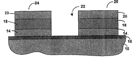
Fig. 5 A illustrates the vertical view of structure shown in Figure 5.As can be understood, Ti-C layer 16 reveals by interconnection layer.The residual surface that is covered by interconnection layer has kept.Therefore, top layer (Ti layer 20) is unique visible other materials in this view.Ti-C layer 16 has formed the resistor that can be coupled to integrated circuit (IC)-components by the processing of other interconnection layers, this will be hereinafter with reference to the accompanying drawings 6 and 6A further specify.
Fig. 6 illustrates and further prepares using Ti-C layer 16 to form resistor.Fig. 6 A illustrates the vertical view of structure shown in Figure 6.Photoresist can be used to the further patterning of interconnection layer so that independently terminal area 24,26 to be provided. Terminal area 24,26 patternings are formed and can be electrically coupled to integrated circuit (IC)-components (such as, high resistance measurement device LED) by terminal area 24,26 to isolate Ti-C layer 16.Therefore, the structure of terminal area 24,26 will be according to application change.In this one exemplary embodiment, patterning forms simple linear resistor, and it is shown by Fig. 6 A well.
Two step etching technics can implement to form the structure with reference to shown in figure 6 and Fig. 6 A.At first, the photoresist patterning is formed the structure of desirable terminal area 24,26.As with reference to the accompanying drawings 5 and the etching technics of 5A explanation, for example interconnection layer is etched into the surface of Ti-C layer 16 by chemical etchant.Those of ordinary skill in the art will be readily appreciated that, need to deposit, shelter with lithographic technique and make up structure shown in Fig. 6 and Fig. 6 A.Although carrying out first etching, one exemplary embodiment of the present invention comes the structure of patterning shown in Fig. 5 and Fig. 5 A, carry out second etching and come the structure of further patterning shown in Fig. 6 and Fig. 6 A, come the etching interconnection layer but can implement single etch step, make the Ti-C layer 16 that underlies reveal.
By after for example wet-etching technology has been removed interconnection layer, can use the Ti-C layer 16 that comes etching to underlie as the dry etch process of plasma etching.For example, can use and O
2The CF that mixes
4Gas is implemented dry plasma.Plasma etching will be removed any zone that resistive Ti-C layer 16 is exposed to gas/pdp body.Therefore, can apply photoresist mask on Ti-C layer 16 area exposed, it will be retained to form resistor.In the present embodiment shown in Fig. 6 and Fig. 6 A, in opening 22, can apply thin bar shaped photoresist, and with its patterning to cover Ti-C layer 16 narrow zone as shown in Figure 6A.Plasma etching is removed Ti-C layer 16 any area exposed.During plasma etching, Ti-C will be removed by the zone that protectiveness photoresist or interconnection layer cover.Therefore, near the flexible substrate 10 that is etched and underlies of the zone terminal area 24,26 to appear.Shown in Fig. 6 and Fig. 6 A, remaining structure has formed the resistance region (bar shaped Ti-C material 16) that is coupling between the terminal area 24,26.Fig. 6 A provides the vertical view of such final structure, wherein, can see the top layer of Ti inculating crystal layer 20 for interconnection, and the remainder of Ti-C layer 16 is coupling between the terminal area 24,26, makes to form resistor on the surface of flexible substrate 10.As previously mentioned, resistor can be patterned and form any desired shape.
Fig. 7-12A illustrates the interchangeable exemplary technique of preparation high resistance measurement device (scope is 100 ohm-1M ohm).Such as will become clear, many preparation processes and material are with as above identical with material with reference to the described step of figure 1-6A.For fear of repetition, some concrete details have been omitted in the following discussion.But the exemplary technique of discussing with reference to figure 7-12A should be understood based on as above describing with reference to the described complete process of figure 1-6A and material.
Beginning please refer to Fig. 7, shows flexible substrate 28.As previously mentioned, flexible substrate 28 generally comprises polyimide-based material.Initial, for example on flexible substrate 28, deposit masking layer (such as, titanium (Ti) layer 30) by physical vapor deposition (PVD) technology.In this one exemplary embodiment, the thickness of the Ti layer 30 that is deposited can be 300 dusts-1000 dust for example.In this one exemplary embodiment, Ti layer 30 will be controlled the zone that flexible substrate 28 will be activated as activation mask, just as will be described as further below.
With reference to figure 8, in Ti layer 30, etch opening 32.Ti layer 30 can use photoresist and optical mask patternization, then for example by implementing to use the wet chemical etch process of hydrofluoric acid (HF) solution with its etching.Opening 32 is patterned as the desired size in zone to be activated.Therefore, opening 32 provides a window to appear part flexible substrate 28.Fig. 8 A is the vertical view of structure shown in Figure 8.Shown in figure 8A, except that appearing by opening 32 (Fig. 8) the zone that is etched of the flexible substrate 28 that underlies, the surface of flexible substrate 28 is covered by Ti layer 30 fully.
Next, as shown in Figure 9, flexible substrate 28 by opening 32 area exposed through high energy argon (Ar) ion bombardment effects with activation flexible substrate 28 area exposed.As previously mentioned, argon (Ar) ion bombardment on flexible substrate 28 surfaces is caused the preferential scission of link of imines carbonyl and forms graphite-like carbon, so formed the activating area 34 that the other materials that can accept and be introduced forms the flexible substrate 28 of carbide bonding.Be easy to make up the active region that forms high resistance area with other materials by providing, activating area 34 can be used to form the electric resistance structure of high value.As can be understood, Ti layer 30 provides the mask that is used for planar magnetic control sputtering (ion bombardment) technology, and the zone that makes flexible substrate 28 be activated only is the zone (that is the zone that appears by opening 32) that is not covered by Ti layer 30.Provide the selectivity opening by patterning Ti layer 30, the shape of resistance region has been determined, has been reduced thus as in the previous examples with reference to figure 6 and the described subsequent step that forms the resistance geometric areas by plasma etching of 6A.In addition, in this one exemplary embodiment, implement Ti layer 30 masking layer is provided.Titanium is used to avoid the pollution in the magnetron sputtering chamber.But, also can use other materials that masking layer is provided.
As shown in figure 10, after forming activating area 34, remove masking layer (Ti layer 30) fully.For example, can implement to use the wet chemical etch process of hydrofluoric acid (HF) solution to come etching Ti layer 30.So remaining structure comprises the flexible substrate 28 of the activating area 34 with patterning.
Next, as shown in figure 11, interconnection layer is arranged on the surface of flexible substrate 28.At first, use is as PVD deposition techniques titanium (Ti) layer 36 of planar magnetic control sputtering.For example, the thickness of set Ti layer 36 can be 300 dusts-1000 dust for example.Because Ti layer 36 is arranged on the flexible substrate 28, activating area 34 react consumingly with titanium (Ti), the electric charge transfer occurs via the carbonyl of activating area 34.As shown in figure 11, along with Ti layer 36 coverage rate increase, in active region 34, formed thin titanium carbide (Ti-C) layer 38.As previously mentioned, Ti-C layer 38 is highly ohmic, so can be used in the resistor for preparing high value (100k ohm-1M ohm) on the surface of flexible substrate 28.
Further as shown in figure 11, at depositing Ti layer 36 with after forming Ti-C layer 38, other interconnection materials can be set on Ti layer 36.For example, can use physical vapor deposition (PVD) technology deposited copper (Cu) inculating crystal layer 40 on Ti layer 36.For example, the thickness of set Cu inculating crystal layer 40 can be 3000 dusts.Next, can electroplate Cu inculating crystal layer 40.At last, for example, can titanium (Ti) inculating crystal layer 42 be set by PVD technology on Cu inculating crystal layer 40 and finish interconnection.Ti inculating crystal layer 42 is that optionally the thickness of setting for example can be 1000 dusts.
Because Ti-C layer 38 has been patterned as useful resistor, only Sheng step forms terminal area by interconnection layer being patterned as desirable pattern exactly.Figure 12 illustrates and forms terminal area 44,46.Figure 12 A illustrates the vertical view of structure shown in Figure 12.Can use photoresist with the interconnection layer patterning so that independently terminal area 44,46 to be provided.After with the photoresist patterning, for example can interconnection layer be etched into the surface of flexible substrate 28 by chemical etchant.As previously mentioned, terminal area 44,46 is patterned to isolate Ti-C layer 38 and forms and can be electrically coupled to integrated circuit (IC)-components (such as, high resistance measurement device LED) by terminal area 44,46.Therefore, the structure of terminal area 44,46 will be according to application change.In this one exemplary embodiment, patterning has formed simple linear resistor, and it is shown by Figure 12 A well.Those of ordinary skill in the art will be readily appreciated that, need to deposit, shelter with lithographic technique and make up structure shown in Figure 12 and Figure 12 A.
As previously mentioned, can be used in many application according to the exemplary high resistance measurement device of present technique preparation on flexible substrate.For example, can on the back side of flexible substrate, form resistance and prevent the infringement of static discharge light-emitting diode (LED) so that the high value bleeder resistor to be provided.Therefore, Figure 13 and Figure 14 illustrate the exemplary embodiment of present technique.
Beginning with reference to Figure 13, illustrates the cross-sectional view of the exemplary led array 48 of preparation on flexible substrate 50.Except led array 48 preparation this fact on the flexible substrate 50, the specific embodiment of the method for this array and this array of preparation is for should be with unimportant.Therefore, the explanation to led array 48 should not be considered to by any way current disclosed structure be limited below, and only means the exemplary use to the illustrated electric resistance structure of this paper.
As previously mentioned, flexible substrate 50 generally includes polyimide-based material, such as
 Use tack coat 54,
 rigid carrier 52 can be attached on the flexible substrate 50.Rigid carrier 52 for example can comprise ceramic material, plastics or macromolecular material that can compression molding.Tack coat 54 for example can comprise anisotropic conductive adhesive.Each rigid carrier 52 comprises led chip 56.Led chip 56 for example can use clad material 58 (such as, epoxy, glass fill epoxy or as the polymeric material of silicones) center on.Each LED structure also comprises lens arrangement 60, and it can comprise radioparent any suitable material to LED, such as layer of polycarbonate.Lens arrangement 60 has improved the light output of led chip 56.
Each rigid carrier 52 also comprises a plurality of feed-through conductive elements, such as being used for led chip 56 is electrically coupled to the electrode 62 of rigid carrier 52 downsides.Electrode 62 is coupled to anisotropic conductive adhesive layer 54.Conductive interconnect paths 64 provides the conductive path by flexible substrate 50.As can be understood, conductive interconnect paths 64 can comprise the path of being filled by electric conducting material.Interconnection path 64 is electrically coupled to the interconnection layer 66 at flexible substrate 50 downsides.Therefore, conductive path is from led chip 56 to electrode 62, through anisotropic conductive adhesive layer 54, through interconnection path 64 and arrive interconnection layer 66 at flexible substrate 50 downsides.These interconnection layers 66 can form the terminal according to the electric resistance structure of the techniques described herein preparation.
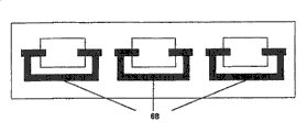
Figure 14 illustrates the rear view for preparing the flexible substrate 50 that bleeder resistance 68 is arranged according to the techniques described herein thereon.As is understood, resistance 68 has advantageously provided the electrical pathways that is used for discharge of electricity.Resistor 68 and terminal area can be prepared as exemplary pattern shown in Figure 14.With resistor 68 patternings with after preparing on flexible substrate 50, can form led array 48 and protection that provides on resistor 68 led chip 56 is provided for it, make its infringement of avoiding static discharge, foregoing such.
Although the present invention can carry out various modifications easily and have other forms, this paper illustrates specific embodiment by way of example by accompanying drawing, and it is had been described in detail.But, should be appreciated that, do not plan to limit the invention to particular forms disclosed.On the contrary, the present invention falls into covering modifications all within the spirit and scope of the invention that claims define, is equal to and replaceable form.For example, although this paper has mentioned the resistor that forms in conjunction with semiconductor LED, these technology can be applied to other LED types equally, such as organic LED.Similarly, can be applied in the luminous field by resistor provided by the present invention and this field outside the Electrical and Electronic circuit in.
Claims (17)
1. one kind prepares method of resistor, and described method comprises the steps:
(a), activation flexible substrate (10) (28) lip-deep zone, form activating area (12) (34) thus;
(b), in described activating area (12) (34), form resistive layer (16) (38), wherein go up depositing metal layers (14) (36) at described activating area (12) (34), thus at described activating area (12) (34) thus in produce to react and form described resistive layer (16) (38);
(c), deposition one or more layers interconnection layer (18,20) (40,42) at least a portion of described resistive layer (16) (38); And
(d), described one or more layers interconnection layer of patterning (18,20) (40,42) forms the terminal (24,26) (44,46) of resistor.
2. method according to claim 1, wherein step (a) comprises the step that ion etching is carried out on described flexible substrate (10) (28) surface.
3. method according to claim 1, wherein step (a) comprises the step in the lip-deep zone of activation polyimide substrate (10) (28).
4. method according to claim 1, wherein the step of depositing metal layers (14) (36) is included in the step that described activating area (12) (34) is gone up deposition titanium layer (14) (36), thus at described activating area (12) (34) thus in produce reaction formation titanium carbide layer (16) (38).
5. method according to claim 1, wherein step (c) is included in the step that goes up copper layer (18) (40) to the described metal level of small part (14) (36).
6. method according to claim 5, wherein step (c) is included in the step that described copper layer (18) (40) is gone up deposition titanium layer (20) (42).
7. semiconductor device comprises:
Flexible substrate;
Be formed on the described flexible substrate and have first end and the resistance region of second end; And
Be coupled in described first end and described second end conducting terminal of each;
Wherein said resistance region is formed in the described activating area of described flexible substrate by activating area and the reaction that is arranged between the metal of this activating area.
8. semiconductor device according to claim 7, wherein said flexible substrate comprises polyimide material.
9. semiconductor device according to claim 7, wherein said resistance region have the resistance of 300k ohm to 1M ohm scope.
10. semiconductor device according to claim 7, wherein said resistance region comprises metal carbides.
11. semiconductor device according to claim 7, wherein said resistance region comprises titanium carbide.
12. semiconductor device according to claim 7, wherein said resistance region forms in the temperature that is lower than 200 ℃.
13. semiconductor device according to claim 7, wherein said resistance region does not comprise serpentine configuration.
14. semiconductor device according to claim 7, each of wherein said conducting terminal comprise first titanium layer.
15. semiconductor device according to claim 14, each of wherein said conducting terminal comprise the copper layer that is arranged on described first titanium layer.
16. semiconductor device according to claim 15, each of wherein said conducting terminal comprise second titanium layer that is arranged on the described copper layer.
17. semiconductor device according to claim 7 comprises each the light-emitting diode that is electrically coupled to described conducting terminal.
Applications Claiming Priority (2)
| Application Number | Priority Date | Filing Date | Title |
|---|---|---|---|
| US10/261,052 | 2002-09-30 | ||
| US10/261,052 US6709944B1 (en) | 2002-09-30 | 2002-09-30 | Techniques for fabricating a resistor on a flexible base material |
Publications (2)
| Publication Number | Publication Date |
|---|---|
| CN1695209A CN1695209A (en) | 2005-11-09 |
| CN100477021C true CN100477021C (en) | 2009-04-08 |
Family
ID=31977937
Family Applications (1)
| Application Number | Title | Priority Date | Filing Date |
|---|---|---|---|
| CNB038250748A Expired - Fee Related CN100477021C (en) | 2002-09-30 | 2003-08-28 | Techniques for fabricating a resistor on a flexible base material |
Country Status (7)
| Country | Link |
|---|---|
| US (2) | US6709944B1 (en) |
| EP (1) | EP1550140A1 (en) |
| JP (1) | JP2006501670A (en) |
| KR (1) | KR20050065565A (en) |
| CN (1) | CN100477021C (en) |
| AU (1) | AU2003268263A1 (en) |
| WO (1) | WO2004032154A1 (en) |
Families Citing this family (47)
| Publication number | Priority date | Publication date | Assignee | Title |
|---|---|---|---|---|
| US20100038121A1 (en) * | 1999-08-27 | 2010-02-18 | Lex Kosowsky | Metal Deposition |
| US7825491B2 (en) * | 2005-11-22 | 2010-11-02 | Shocking Technologies, Inc. | Light-emitting device using voltage switchable dielectric material |
| US20100044079A1 (en) * | 1999-08-27 | 2010-02-25 | Lex Kosowsky | Metal Deposition |
| US20100040896A1 (en) * | 1999-08-27 | 2010-02-18 | Lex Kosowsky | Metal Deposition |
| US20100044080A1 (en) * | 1999-08-27 | 2010-02-25 | Lex Kosowsky | Metal Deposition |
| US20100038119A1 (en) * | 1999-08-27 | 2010-02-18 | Lex Kosowsky | Metal Deposition |
| AU6531600A (en) * | 1999-08-27 | 2001-03-26 | Lex Kosowsky | Current carrying structure using voltage switchable dielectric material |
| US20080035370A1 (en) * | 1999-08-27 | 2008-02-14 | Lex Kosowsky | Device applications for voltage switchable dielectric material having conductive or semi-conductive organic material |
| KR100674824B1 (en) | 2004-12-08 | 2007-01-25 | 삼성전기주식회사 | Manufacturing method of magneto-resistive device |
| EP1750309A3 (en) * | 2005-08-03 | 2009-07-29 | Samsung Electro-mechanics Co., Ltd | Light emitting device having protection element |
| US20100264224A1 (en) * | 2005-11-22 | 2010-10-21 | Lex Kosowsky | Wireless communication device using voltage switchable dielectric material |
| US7923844B2 (en) * | 2005-11-22 | 2011-04-12 | Shocking Technologies, Inc. | Semiconductor devices including voltage switchable materials for over-voltage protection |
| US8222116B2 (en) | 2006-03-03 | 2012-07-17 | Semiconductor Energy Laboratory Co., Ltd. | Method for manufacturing semiconductor device |
| US20080029405A1 (en) * | 2006-07-29 | 2008-02-07 | Lex Kosowsky | Voltage switchable dielectric material having conductive or semi-conductive organic material |
| US7981325B2 (en) * | 2006-07-29 | 2011-07-19 | Shocking Technologies, Inc. | Electronic device for voltage switchable dielectric material having high aspect ratio particles |
| US20080032049A1 (en) * | 2006-07-29 | 2008-02-07 | Lex Kosowsky | Voltage switchable dielectric material having high aspect ratio particles |
| WO2008036423A2 (en) | 2006-09-24 | 2008-03-27 | Shocking Technologies, Inc. | Formulations for voltage switchable dielectric material having a stepped voltage response and methods for making the same |
| US20120119168A9 (en) * | 2006-11-21 | 2012-05-17 | Robert Fleming | Voltage switchable dielectric materials with low band gap polymer binder or composite |
| JP5374063B2 (en) * | 2007-03-28 | 2013-12-25 | 三菱重工業株式会社 | Metal melting crucible and surface treatment method thereof |
| US7793236B2 (en) * | 2007-06-13 | 2010-09-07 | Shocking Technologies, Inc. | System and method for including protective voltage switchable dielectric material in the design or simulation of substrate devices |
| US20100006884A1 (en) * | 2007-08-07 | 2010-01-14 | Epistar Corporation | Light Emitting Device and Manufacturing Method Therof |
| US8206614B2 (en) | 2008-01-18 | 2012-06-26 | Shocking Technologies, Inc. | Voltage switchable dielectric material having bonded particle constituents |
| US8203421B2 (en) * | 2008-04-14 | 2012-06-19 | Shocking Technologies, Inc. | Substrate device or package using embedded layer of voltage switchable dielectric material in a vertical switching configuration |
| US7727808B2 (en) * | 2008-06-13 | 2010-06-01 | General Electric Company | Ultra thin die electronic package |
| US20100047535A1 (en) * | 2008-08-22 | 2010-02-25 | Lex Kosowsky | Core layer structure having voltage switchable dielectric material |
| WO2010033635A1 (en) * | 2008-09-17 | 2010-03-25 | Shocking Technologies, Inc. | Voltage switchable dielectric material containing boron compound |
| US9208931B2 (en) | 2008-09-30 | 2015-12-08 | Littelfuse, Inc. | Voltage switchable dielectric material containing conductor-on-conductor core shelled particles |
| EP2342722A2 (en) * | 2008-09-30 | 2011-07-13 | Shocking Technologies Inc | Voltage switchable dielectric material containing conductive core shelled particles |
| US8362871B2 (en) * | 2008-11-05 | 2013-01-29 | Shocking Technologies, Inc. | Geometric and electric field considerations for including transient protective material in substrate devices |
| US9226391B2 (en) | 2009-01-27 | 2015-12-29 | Littelfuse, Inc. | Substrates having voltage switchable dielectric materials |
| US8272123B2 (en) | 2009-01-27 | 2012-09-25 | Shocking Technologies, Inc. | Substrates having voltage switchable dielectric materials |
| US8399773B2 (en) | 2009-01-27 | 2013-03-19 | Shocking Technologies, Inc. | Substrates having voltage switchable dielectric materials |
| KR101679099B1 (en) | 2009-03-26 | 2016-11-23 | 쇼킹 테크놀로지스 인코포레이티드 | Components having voltage switchable dielectric materials |
| US9053844B2 (en) * | 2009-09-09 | 2015-06-09 | Littelfuse, Inc. | Geometric configuration or alignment of protective material in a gap structure for electrical devices |
| KR101065409B1 (en) * | 2009-11-04 | 2011-09-16 | 삼성모바일디스플레이주식회사 | Organic light emitting diode lighting apparatus |
| US20110198544A1 (en) * | 2010-02-18 | 2011-08-18 | Lex Kosowsky | EMI Voltage Switchable Dielectric Materials Having Nanophase Materials |
| US9224728B2 (en) * | 2010-02-26 | 2015-12-29 | Littelfuse, Inc. | Embedded protection against spurious electrical events |
| US9082622B2 (en) | 2010-02-26 | 2015-07-14 | Littelfuse, Inc. | Circuit elements comprising ferroic materials |
| US9320135B2 (en) * | 2010-02-26 | 2016-04-19 | Littelfuse, Inc. | Electric discharge protection for surface mounted and embedded components |
| CN102324289B (en) * | 2011-05-31 | 2014-05-14 | 四平市吉华高新技术有限公司 | Thick-film resistor board and manufacturing method thereof |
| TWI497535B (en) | 2011-07-28 | 2015-08-21 | Cyntec Co Ltd | Micro-resistive device with soft material layer and manufacture method for the same |
| CN102903467B (en) * | 2011-07-29 | 2016-04-06 | 乾坤科技股份有限公司 | There is micro-resistive element and the manufacture method thereof of flexible material layer |
| DE102012208730A1 (en) * | 2012-05-24 | 2013-11-28 | Osram Opto Semiconductors Gmbh | Optoelectronic component device and method for producing an optoelectronic component device |
| DE102015000380A1 (en) * | 2015-01-13 | 2016-07-14 | Wabco Gmbh | Sensor unit, sensing and evaluation device with such a sensor unit and motor vehicle or trailer with it and method for protecting an evaluation |
| CN111780653B (en) * | 2020-06-09 | 2022-01-07 | 中国电子科技集团公司第四十九研究所 | Carbon film nano conductive material-based resistor and preparation method thereof |
| WO2022182620A1 (en) * | 2021-02-26 | 2022-09-01 | KYOCERA AVX Components Corporation | High frequency and high power thin-film component |
| CN113410382B (en) * | 2021-06-15 | 2022-11-29 | 西安微电子技术研究所 | Chromium-silicon film resistor and preparation method thereof |
Family Cites Families (12)
| Publication number | Priority date | Publication date | Assignee | Title |
|---|---|---|---|---|
| GB1319765A (en) * | 1969-10-15 | 1973-06-06 | Atomic Energy Authority Uk | Resistive elements |
| US3966578A (en) * | 1974-01-17 | 1976-06-29 | Ceramic Magnetics, Inc. | Method of making thin film thermistor |
| US4485297A (en) * | 1980-08-28 | 1984-11-27 | Flexwatt Corporation | Electrical resistance heater |
| US5250388A (en) * | 1988-05-31 | 1993-10-05 | Westinghouse Electric Corp. | Production of highly conductive polymers for electronic circuits |
| US5065502A (en) * | 1988-09-30 | 1991-11-19 | Lucas Duralith Art Corporation | Method for modifying electrical performance characteristics of circuit paths on circuit panels |
| KR900014625A (en) * | 1989-03-20 | 1990-10-24 | 미다 가쓰시게 | Metal / organic polymer synthetic resin composite and preparation method thereof |
| US5340640A (en) * | 1992-03-25 | 1994-08-23 | Molex Incorporated | Conductive ink for use with printed circuit modules |
| JP2816629B2 (en) * | 1992-06-12 | 1998-10-27 | シャープ株式会社 | Light emitting device with built-in resistor |
| US5753523A (en) * | 1994-11-21 | 1998-05-19 | Brewer Science, Inc. | Method for making airbridge from ion-implanted conductive polymers |
| AU6531600A (en) * | 1999-08-27 | 2001-03-26 | Lex Kosowsky | Current carrying structure using voltage switchable dielectric material |
| US6936855B1 (en) * | 2002-01-16 | 2005-08-30 | Shane Harrah | Bendable high flux LED array |
| US6932518B2 (en) * | 2002-03-19 | 2005-08-23 | Finisar Corporation | Circuit board having traces with distinct transmission impedances |
-
2002
- 2002-09-30 US US10/261,052 patent/US6709944B1/en not_active Expired - Lifetime
-
2003
- 2003-08-28 EP EP03749217A patent/EP1550140A1/en not_active Withdrawn
- 2003-08-28 WO PCT/US2003/027112 patent/WO2004032154A1/en active Application Filing
- 2003-08-28 CN CNB038250748A patent/CN100477021C/en not_active Expired - Fee Related
- 2003-08-28 KR KR1020057005388A patent/KR20050065565A/en not_active Application Discontinuation
- 2003-08-28 JP JP2004541496A patent/JP2006501670A/en active Pending
- 2003-08-28 AU AU2003268263A patent/AU2003268263A1/en not_active Abandoned
- 2003-11-18 US US10/716,143 patent/US7158383B2/en not_active Expired - Lifetime
Also Published As
| Publication number | Publication date |
|---|---|
| EP1550140A1 (en) | 2005-07-06 |
| KR20050065565A (en) | 2005-06-29 |
| WO2004032154A1 (en) | 2004-04-15 |
| CN1695209A (en) | 2005-11-09 |
| JP2006501670A (en) | 2006-01-12 |
| US20040114336A1 (en) | 2004-06-17 |
| US7158383B2 (en) | 2007-01-02 |
| AU2003268263A1 (en) | 2004-04-23 |
| US6709944B1 (en) | 2004-03-23 |
| US20040063294A1 (en) | 2004-04-01 |
Similar Documents
| Publication | Publication Date | Title |
|---|---|---|
| CN100477021C (en) | Techniques for fabricating a resistor on a flexible base material | |
| US7629691B2 (en) | Conductor geometry for electronic circuits fabricated on flexible substrates | |
| KR100731244B1 (en) | Method of processing absorbed material and electrostatic absorption method | |
| US20110026187A1 (en) | Conductive Seal Ring Electrostatic Chuck | |
| JPH0779122B2 (en) | Electrostatic chuck with diamond coating | |
| TW200402121A (en) | Method of forming a through-substrate interconnect | |
| US7084067B2 (en) | Removal of copper oxides from integrated interconnects | |
| JP2694668B2 (en) | Substrate holding device | |
| TW497282B (en) | Semiconductor-chip and its production method | |
| CN102460687B (en) | Laminated wiring board | |
| JP4396754B2 (en) | Method for electrically connecting element to wiring and method for manufacturing light emitting element assembly | |
| US20060231919A1 (en) | Passive microwave device and method for producing the same | |
| TW367578B (en) | Manufacturing method for unlanded via | |
| US6993828B2 (en) | Method for manufacturing metal thin film resistor | |
| CN111009489B (en) | Preparation method of metal substrate | |
| US3956820A (en) | Method of manufacturing a semiconductor device having a lead bonded to a surface thereof | |
| JP2002343995A5 (en) | ||
| EP0200237A2 (en) | Process to obtain thin film lines | |
| KR100585032B1 (en) | Electrode of plasma processing apparatus and manufacturing method thereof | |
| KR100975628B1 (en) | Method for manufacturing a thin film flexible thermoelectric module using peeling process | |
| JP2003121466A (en) | Probe unit and its manufacturing method | |
| JP2643004B2 (en) | Hybrid IC substrate | |
| CN114975750A (en) | Display device, processing method and display equipment | |
| Spasos et al. | A novel design for an RF MEMS resistive switch on PCB substrate | |
| TW429526B (en) | Manufacturing method for salicide contact |
Legal Events
| Date | Code | Title | Description |
|---|---|---|---|
| C06 | Publication | ||
| PB01 | Publication | ||
| C10 | Entry into substantive examination | ||
| SE01 | Entry into force of request for substantive examination | ||
| C14 | Grant of patent or utility model | ||
| GR01 | Patent grant | ||
| C17 | Cessation of patent right | ||
| CF01 | Termination of patent right due to non-payment of annual fee |
Granted publication date: 20090408 Termination date: 20090928 |