CN100432974C - Data transfer control device and electronic instrument - Google Patents
Data transfer control device and electronic instrument Download PDFInfo
- Publication number
- CN100432974C CN100432974C CNB2006100653944A CN200610065394A CN100432974C CN 100432974 C CN100432974 C CN 100432974C CN B2006100653944 A CNB2006100653944 A CN B2006100653944A CN 200610065394 A CN200610065394 A CN 200610065394A CN 100432974 C CN100432974 C CN 100432974C
- Authority
- CN
- China
- Prior art keywords
- data
- bag
- perhaps
- transfer controller
- data transfer
- Prior art date
- Legal status (The legal status is an assumption and is not a legal conclusion. Google has not performed a legal analysis and makes no representation as to the accuracy of the status listed.)
- Expired - Fee Related
Links
Images


Classifications
-
- G—PHYSICS
- G06—COMPUTING; CALCULATING OR COUNTING
- G06F—ELECTRIC DIGITAL DATA PROCESSING
- G06F13/00—Interconnection of, or transfer of information or other signals between, memories, input/output devices or central processing units
- G06F13/14—Handling requests for interconnection or transfer
-
- H—ELECTRICITY
- H04—ELECTRIC COMMUNICATION TECHNIQUE
- H04L—TRANSMISSION OF DIGITAL INFORMATION, e.g. TELEGRAPHIC COMMUNICATION
- H04L12/00—Data switching networks
- H04L12/28—Data switching networks characterised by path configuration, e.g. LAN [Local Area Networks] or WAN [Wide Area Networks]
- H04L12/40—Bus networks
- H04L12/40052—High-speed IEEE 1394 serial bus
- H04L12/40117—Interconnection of audio or video/imaging devices
-
- G—PHYSICS
- G06—COMPUTING; CALCULATING OR COUNTING
- G06F—ELECTRIC DIGITAL DATA PROCESSING
- G06F13/00—Interconnection of, or transfer of information or other signals between, memories, input/output devices or central processing units
- G06F13/38—Information transfer, e.g. on bus
-
- G—PHYSICS
- G06—COMPUTING; CALCULATING OR COUNTING
- G06F—ELECTRIC DIGITAL DATA PROCESSING
- G06F13/00—Interconnection of, or transfer of information or other signals between, memories, input/output devices or central processing units
- G06F13/38—Information transfer, e.g. on bus
- G06F13/40—Bus structure
- G06F13/4004—Coupling between buses
- G06F13/4027—Coupling between buses using bus bridges
- G06F13/4045—Coupling between buses using bus bridges where the bus bridge performs an extender function
-
- H—ELECTRICITY
- H04—ELECTRIC COMMUNICATION TECHNIQUE
- H04L—TRANSMISSION OF DIGITAL INFORMATION, e.g. TELEGRAPHIC COMMUNICATION
- H04L69/00—Network arrangements, protocols or services independent of the application payload and not provided for in the other groups of this subclass
- H04L69/22—Parsing or analysis of headers
-
- Y—GENERAL TAGGING OF NEW TECHNOLOGICAL DEVELOPMENTS; GENERAL TAGGING OF CROSS-SECTIONAL TECHNOLOGIES SPANNING OVER SEVERAL SECTIONS OF THE IPC; TECHNICAL SUBJECTS COVERED BY FORMER USPC CROSS-REFERENCE ART COLLECTIONS [XRACs] AND DIGESTS
- Y02—TECHNOLOGIES OR APPLICATIONS FOR MITIGATION OR ADAPTATION AGAINST CLIMATE CHANGE
- Y02D—CLIMATE CHANGE MITIGATION TECHNOLOGIES IN INFORMATION AND COMMUNICATION TECHNOLOGIES [ICT], I.E. INFORMATION AND COMMUNICATION TECHNOLOGIES AIMING AT THE REDUCTION OF THEIR OWN ENERGY USE
- Y02D10/00—Energy efficient computing, e.g. low power processors, power management or thermal management
Abstract
A data transfer control device includes: an interface circuit to which data of which one data unit is K bits is input through an interface bus; and a link controller which generates a packet transmitted through a serial bus. The link controller includes: a data formatter which generates (NI)-byte packed data containing M pieces of (K+L)-bit data obtained by adding L bits of dummy data to the K-bit data, the data formatter generating the packed data in which L and M are variably set corresponding to K; and a packet generation circuit which generates a packet in which the packed data is inserted in a data field.
Description
Technical field
The present invention relates to data transfer controller and electronic equipment.
Background technology
In recent years, as being the interface of purpose to reduce EMI noise etc., (the low-voltage differential signal transmission: Low Voltage Differential Signaling) etc. high speed serial transmission interface attracts tremendous attention as LVDS.In this high speed serial transmission, transmitter circuit utilizes differential wave (Differential Signals) to send serialized data, and acceptor circuit is with the differential amplification of differential wave, thus the realization data transmission.
Conventional cellular phone comprises: first battery limits are provided with the button of importing telephone number and character; Liquid CrystalDisplay), sub-LCD or camera (CCD) second battery limits are provided with main LCD (LCD:; And the bonding pad, connect the hinge of first, second battery limits etc.In this case,, be arranged at first substrate of first battery limits and be arranged at data transmission between second substrate of second battery limits, can reduce quantity, reach better effects by the distribution of bonding pad by utilizing the serial transmission mode of differential wave.
But, various forms are arranged from the camera data of cameras such as CCD or CMOS (camera head) output.Specifically, forms such as YUV 422, YUV 420, RGB 888, RGB 565, RGB 444, RAW 6, RAW 7, RAW 8, RAW 10, RAW 12, JPEG 8 are arranged.At this, YUV 422 and YUV 420 be as 8 data (data unit is 8 data) input, RGB 888 as 24 data, RGB565 as 16, RGB 444 data input as 12.In addition, as 6,7,8,10,12 data input, JPEG 8 imports as 8 data respectively for RAW 6, RAW 7, RAW 8, RAW 10, RAW 12.Thereby when with the camera data subpackage, when being provided with the first battery limits serial transmission of host apparatus, hope can be supported these multiple forms from second battery limits that are provided with camera.
But when with the camera data subpackage of these multiple forms, it is many that the figure place of redundant data will become, and it is big that the volume of transmitted data in the universal serial bus will become.On the other hand, be 0 and corresponding if want to make the figure place of redundant data with above-mentioned multiple form, then will cause the problems such as expansion of circuit scale.
Patent documentation 1: the spy opens the 2001-222249 communique
Summary of the invention
The present invention has overcome above-mentioned technical matters, its purpose be to provide a kind of can be in extensiveization that suppresses circuit, realize the data transfer controller of efficient serial transmission of multiple formatted data and the electronic equipment that comprises this device.
The present invention relates to a kind of data transfer controller, be used for control data transmission, it comprises: interface circuit is transfused to the data that a data unit is K position (K is the integer more than or equal to 2) by interface circuit; Link controller, the bag that generation sends by universal serial bus, described link controller comprises: data formatter, generation contain M (K+L) position (L is the integer more than or equal to 0) data ((N, I, M are the integers more than or equal to the 1) packed data of byte of N * I), data that should (K+L) position are by obtaining the pseudo-data in the additional L position of the described data of K position; The bag generative circuit generates described packed data and is inserted into bag in the data field, and as the bag that sends by described universal serial bus, described data formatter generates the described packed data that described L and M are set changeably according to described K.
According to the present invention, generate the packed data that L and M are set changeably according to K, this packed data contains the M (data of byte of N * I) by (K+L) position that the pseudo-data in the additional L position of the described data of K position are then obtained.And this packed data inserts (setting) in the data field of the bag that sends by universal serial bus.The L of packed data is set changeably by K like this, thereby can reduces the volume of transmitted data in the universal serial bus.In addition, by the M of packed data is set changeably according to K, can suppress extensiveization of circuit.Thereby,, when suppressing circuit scale, can realize the efficient serial transmission of multiple formatted data according to the present invention.
In addition, in the present invention, described data formatter also can generate following packed data: when K=6, I=1, L=0, M=4, N=3, perhaps when K=7, I=1, L-1, M=2, N=2, perhaps when K=8, I=1, L=0, M=2, N=2, perhaps when K=10, I=1, L=2, M=2, N=3, perhaps when K=12, I=1, L=0, M=2, N=3, perhaps when K=16, I=1, L=0, M=1, N=2, perhaps when K=24, I=1, L=0, M=1, N=3.In addition, also can adopt form outside above-mentioned.
In addition, in the present invention, described data formatter also can generate following packed data: when K=6, I=2, L=0, M=8, N=3, perhaps when K=7, I=2, L=1, M=4, N=2, perhaps when K=8, I=2, L=0, M=4, N=2, perhaps when K=10, I=2, L=1, M=3, N=2, perhaps when K=12, I=2, L=0, M=4, N=3, perhaps when K=16, I=2, L=0, M=2, N=2, perhaps when K=24, I=2, L=0, M=2, N=3.In addition, also can adopt form outside above-mentioned.
In addition, in the present invention, also can be N * 8 * I=(K+L) * M.But, the situation of N * 8 * I=(K+L) * invalid exception of M also can be arranged.
In addition, in the present invention, described bag generative circuit also can insert the configuration information that is used to be provided with described M, N in the header of the bag that sends by described universal serial bus.
Thus, can make the format conversion of the packed data that receiver side carried out of bag become simple.
In addition, in the present invention, also can comprise internal register, storage is used to be provided with the configuration information of described M, N, and described data formatter is inserted described pseudo-data according to described configuration information.
Thus, can make the insertion of pseudo-data handle simplification.In addition, data formatter can be judged insertion position of pseudo-data etc. according to count value in the digit counter or the count value in the byte counter.
In addition, the electronic equipment according to the present invention relates to comprises: the above-mentioned data transfer controller that each is put down in writing; And the one or more devices that are connected in described data transfer controller by described interface bus.
In addition, according to the data transfer controller that the present invention relates to, be the data transfer controller of control data transmission, comprise: interface circuit, carry out data transfer controller and handle by the interface that system bus is connected between host apparatus on the data transfer controller; And link controller, the bag that receives by universal serial bus is resolved, with a data unit is that the data of K position (K is the integer more than or equal to 2) output to described interface circuit, wherein, link controller inserts the packed data that described L and M are set changeably according to described K in the data field of the bag that receives by described universal serial bus, this packed data is the (byte (M of N * I) that contains M (K+L) bit data, N, I is the integer more than or equal to 1) data, should (K+L) bit data obtain by the pseudo-data in the additional L position (L is the integer more than or equal to 0) of described data to the K position, described link controller comprises data formatter, described data formatter outputs in the described interface circuit from the described data of described packed data extraction K position.
According to the present invention, to be inserted into according to the packed data that K is provided with L and M changeably in the data field of the bag that receives by universal serial bus, this packed data be contain M (K+L) bit data (byte (M, N, I are the integers more than or equal to the 1) data of N * I), data that should (K+L) position obtain by the described data of K position are added the pseudo-data in L position (L is the integer more than or equal to 0).And, in data formatter this packed data from the data field that is inserted into bag, extract the data of K position out, output in the interface circuit.Thus, by the L of packed data is set changeably according to K, can reduce the volume of transmitted data in the universal serial bus.In addition, by the M of packed data is set changeably according to K, can suppress extensiveization of circuit.Thereby,, when suppressing extensiveization of circuit, can realize the efficient serial transmission of multiple formatted data according to the present invention.
In addition, in the present invention, be inserted into the described packed data of bag, also can be following data: when K=6, I=1, L=0, M=4, N=3, perhaps when K=7, I=1, L=1, M=2, N=2, perhaps when K=8, I=1, L=0, M=2, N=2, perhaps when K=10, I=1, L=2, M=2, N=3, perhaps when K=12, I=1, L=0, M=2, N=3, perhaps when K=16, I=1, L=0, M=1, N=2, perhaps when K=24, I=1, L=0, M=1, N=3.In addition, also can adopt form outside above-mentioned.
In addition, in the present invention, be inserted into the described packed data of bag, also can be following data: when K=6, I=2, L=0, M=8, N=3, perhaps when K=7, I=2, L=1, M=4, N=2, perhaps when K=8, I=2, L=0, M=4, N=2, perhaps when K=10, I=2, L=1, M=3, N=2, perhaps when K=12, I=2, L=0, M=4, N=3, perhaps when K=16, I=2, L=0, M=2, N=2, perhaps when K=24, I=2, L=0, M=2, N=3.In addition, also can adopt form outside above-mentioned.
In addition, in the present invention, also can be N * 8 * I=(K+L) * M.But, the situation of N * 8 * I=(K+L) * invalid exception of M also can be arranged.
In addition, in the present invention, on the header of the bag that receives by described universal serial bus, insertion is used to be provided with the configuration information of described M, N, described link controller comprises the bag parser circuitry, be used to resolve the header of the bag of reception, described configuration information is extracted out from the header of bag, described data formatter is extracted the described data of K position out from described packed data according to described configuration information.
Thus, the processing of extracting the K bit data from packed data out is oversimplified.
In addition, in the present invention, in the header of the bag that receives by described universal serial bus, insertion is used to be provided with the configuration information of described M, N, described link controller comprises the bag parser circuitry, be used to resolve the header of the bag of reception, described configuration information is extracted out from the header of bag, described data formatter is deleted described pseudo-data according to described configuration information.
Thus, can make the deletion of pseudo-data handle simplification.In addition, data formatter can be judged delete position of pseudo-data etc. according to count value in the digit counter or the count value in the byte counter.
In addition, the electronic equipment that the present invention relates to comprises: above-mentioned each described data transfer controller; And the described host apparatus that is connected in described data transfer controller by described system bus.
Description of drawings
Fig. 1 is the data transfer controller of present embodiment and the configuration example synoptic diagram of system thereof.
Fig. 2 is the data transfer controller of present embodiment and the configuration example synoptic diagram of system thereof.
Fig. 3 (A) and Fig. 3 (B) are the key diagrams of comparative example method.
Fig. 4 (A) and Fig. 4 (B) are the key diagrams of comparative example method.
Fig. 5 is the configuration example synoptic diagram of the data transfer controller of present embodiment.
Fig. 6 is the configuration example synoptic diagram of the data transfer controller of present embodiment.
Fig. 7 (A)~Fig. 7 (D) is the waveform example of camera interface signal.
Fig. 8 is the key diagram of the format conversion method of present embodiment.
Fig. 9 is the key diagram of the format conversion method of present embodiment.
Figure 10 (A) and Figure 10 (B) are the key diagrams of the bag that uses in the present embodiment.
Figure 11 (A), Figure 11 (B) and Figure 11 (C) are the key diagrams of present embodiment advantage.
Figure 12 (A), Figure 12 (B) and Figure 12 (C) are the key diagrams of present embodiment advantage.
Figure 13 is the key diagram of the serial transmission of present embodiment.
Figure 14 is the configuration example synoptic diagram of electronic equipment.
Embodiment
Describe optimum embodiment of the present invention below in detail.In addition, the present embodiment that the following describes is not to being documented in the improper qualification of the content of the present invention in the claim scope, and the whole formations that illustrate in the present embodiment are not all to be necessary as solution of the present invention.
1. system constitutes
Fig. 1 is the data transfer controller (data transfer control circuit) of present embodiment and the synoptic diagram of system's configuration example thereof.In the present embodiment, by the host computer side that uses Fig. 1, the data transfer controller 10,30 of target side, realized the bridging functionality between so-called system bus, interface bus.
In addition, the formation that data transfer controller 10,30 is not limited at Fig. 1 can be omitted a part or the connected mode of change between circuit module of the circuit module of Fig. 1, also can append the circuit module different with Fig. 1.For example, also can in host computer side data transfer controller 10, omit the formation of transceiver 20 or in target side data transfer controller 30, omit the formation of transceiver 40.In addition, data transfer controller 30 and display driver 6 or camera 8 (camera head, camera apparatus) also can be made of twin-core sheet (semi-conductor chip), but also can be made of single-chip.Can constitute by single-chip too for host apparatus 5 (system and device) and data transfer controller 10.
Main frame (TX) side data transmission control unit 10 and target (RX) side data transmission control unit 30, the universal serial bus by differential wave (differntial signals) wraps transmission.More particularly, the transmitting-receiving of wrapping of the differential signal line (differntial signal lines) by current drives or driven universal serial bus.
Host computer side data transfer controller 10 comprises interface circuit 92, this interface circuit 92 carry out and host apparatus 5 (CPU, baseband engine, display controller etc.) between interface handle.This interface circuit 92 is connected on the host apparatus 5 by system bus (host bus).System bus can use as the rgb interface bus, or (MicroProcessor Unit: microprocessor unit) interface bus uses, or uses as serial interface bus, or uses as the camera interface bus as MPU.When using as the rgb interface bus, system bus can comprise the signal wire of horizontal-drive signal, vertical synchronizing signal, clock signal, data-signal etc.When using as the MPU interface bus, system bus can comprise the signal wire of data-signal, read signal, write signal, address 0 signal (command identification signal), chip select signal etc.When using as serial interface bus, system bus can comprise the signal wire of serial line interface with chip select signal, read/write signal, address 0 signal, data-signal, clock signal etc.When using as the camera interface bus, system bus can comprise the signal wire of horizontal-drive signal that camera interface uses, vertical synchronizing signal, clock signal, data-signal etc.
Host computer side data transfer controller 10 comprises the link controller 90 (link layer circuit) that carries out link layer process.This link controller 90 generates by universal serial bus (LVDS) and is transferred to bag in the target side data transfer controller 30 (request package, stream wrap etc.), and sends the processing of the bag of generation.Specifically, this link controller 90 starts the transmission affairs, sends the bag that generates to transceiver 20 indications.
Host computer side data transfer controller 10 comprises the transceiver 20 (PHY) that carries out physical layer process etc.This transceiver 20 will be sent in the target side data transfer controller 30 by universal serial bus by the bag of link controller 90 indications.In addition, transceiver 20 also receives the bag from target side data transfer controller 30.At this moment, link controller 90 is resolved the bag that receives, and carries out the processing of link layer (transaction layer).
Target side data transfer controller 30 comprises the transceiver 40 (PHY) that carries out physical layer process etc.This transceiver 40 is by the bag of universal serial bus reception from host computer side data transfer controller 10.In addition, transceiver 40 also sends bag to host computer side data transfer controller 10.At this moment, link controller 100 generates the bag and the indication that will send and sends the bag that generates.
Target side data transfer controller 30 comprises link controller 100 (link layer circuit).This link controller 100 carries out the reception processing from the bag of host computer side data transfer controller 10, resolves the link layer (transaction layer) of the bag of reception and handles.
Target side data transfer controller 30 comprises interface circuit 110, and this interface circuit 110 carries out and drive the display driver 6 and the processing of the interface between camera 8 (broadly being meant one or more devices) of display panel 7 (LCD etc.).This interface circuit 110 generates the various interface signal, outputs on display driver 6 grades by interface bus.In addition, receive the various interface signal by interface bus from camera 8.This interface circuit 110 can comprise rgb interface circuit, MPU interface circuit, serial interface circuit or camera interface circuits (broadly being the interface circuit of the first~the N) etc.
When the system bus of host computer side (host apparatus 5) used as the rgb interface bus, the interface bus of target side (display driver 6) also used as the rgb interface bus.And interface circuit 110 (rgb interface circuit) generation RGB is with interface signal and output to display driver 6 (broadly being device).In addition, when the system bus of host computer side used as the MPU interface bus, the interface bus of target side also used as the MPU interface bus.And interface circuit 110 (MPU interface circuit) generation MPU is with interface signal and output to display driver 6.In addition, when the system bus of host computer side used as the camera interface bus, the interface bus of target side also used as the camera interface bus.And the interface circuit 110 (camera interface circuits) of target side is from camera 8 receiving interface signals.On the other hand, the interface circuit 92 (camera interface circuits) of host computer side generates the camera interface signal and outputs to host apparatus 5.In addition, also can make the interface shape of system bus and interface bus different.
By above-mentioned interface circuit 92,110 is set, realized the bus bridge function between host computer side system bus and target side interface bus in the present embodiment.
That is, when system bus used as the rgb interface bus, the rgb interface signal that utilization is exported host apparatus 5 by the bag transmission of the universal serial bus of differential wave was transferred to target side.And, the interface circuit 110 of target side will with output to display driver 6 from the corresponding rgb interface signal of the rgb interface signal of host computer side.In addition, when system bus used as the MPU interface bus, the MPU interface signal that utilization is exported host apparatus 5 by the bag transmission of the universal serial bus of differential wave was transferred to target side.And, the interface circuit 110 of target side will with output to display driver 6 from the corresponding MPU interface signal of the MPU interface signal of host computer side.
In addition, when system bus uses as the camera interface bus, utilize the bag transmission by the universal serial bus of differential wave, the camera interface signal (data-signal, vertical synchronizing signal, horizontal-drive signal) that camera 8 is exported is transferred to host computer side from target side.And, the interface circuit 92 of host computer side will with output to host apparatus 5 from the corresponding camera interface signal of the camera interface signal of target side.
In addition, in Fig. 1, the data transfer controller 10 that connects host apparatus 5 is as host computer side (TX), and the data transfer controller 30 that connects camera 8 is as target side (RX), but present embodiment is not limited thereto.For example, as shown in Figure 2, also can will connect the data transfer controller 10 of host apparatus 5 as target side (RX) with the data transfer controller 30 that is connected with camera 8 as host computer side (TX).
That is, in the present embodiment, the data transfer controller of host computer side comprises clock signal generating circuit (PLL circuit), the clock signal that generates is outputed to the data transfer controller of target side.And, under the situation of Fig. 1, the data transfer controller 10 of host computer side, the differential clock signal CLK+ that will generate by clock signal generating circuit/-output in the data transfer controller 30 of target side.So, the data transfer controller 30 of target side according to this CLK+/-generate differential gating signal STB+/-.And, the data transfer controller of target side 30 and STB+/-edge (rising edge or negative edge) synchronous, with differential data signal DTI+/-(camera data) output to the data transfer controller 10 of host computer side.
On the other hand, under situation shown in Figure 2, the data transfer controller 30 of host computer side, by clock signal generating circuit generate differential clock signal CLK+/-.And, the data transfer controller of host computer side 30 and CLK+/-the edge synchronous, with differential data signal DTO+/-(camera data) output in the data transfer controller 10 of target side.
In addition, for use DTO+ as differential wave/-, CLK+/-, DTI+/-, STB+/-the serial transmission method, will in Figure 13 described later, be described in detail.
2. the format conversion of camera data
From the camera data of cameras such as CCD or CMOS output, comprise various forms such as YUV422, YUV 420, RGB 888, RGB 565, RGB 444, RAW 6, RAW 7, RAW 8, RAW 10, RAW 12, JPEG 8.And, in these forms, the figure place difference of the data unit of input data, for example 6,7,8,10,12,16,24 (broadly being the K position).
But,, be by being unit with the byte or being that the data of unit (being unit with the I byte broadly) constitute with the word by the bag of universal serial bus transmission.Thereby, for camera data subpackage parallel series transmission, be necessary 6,7,8,10,12,16 or 24 camera data format conversion to being unit with the byte or being the data of unit (is unit with the I byte) with the word.
Fig. 3 (A) and Fig. 3 (B) and Fig. 4 (A) and Fig. 4 (B) show the method for first, second comparative example of realizing such format conversion.Fig. 3 (A)~Fig. 4 (B) is that the data (camera data) as the format conversion object are the examples of the situation of 10 (RAW 10).And, Fig. 3 (A) and Fig. 3 (B) be with these 10 be the data conversion of unit for being the example of the data conditions of unit with the byte, Fig. 4 (A) and Fig. 4 (B) are to be that the data conversion of unit is to be the example of the data conditions of unit (is unit with the word) with 2 bytes with these 10.
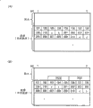
In addition, in Fig. 3 (A) etc., (101) are meant first of first data (10 bit data), and (102) are meant second of first data.In addition, (201) are meant first of second data, and (202) are meant second of second data.Thereby 1~10 of first data is represented in (101)~(110), and 1~10 of second data is represented in (201)~(210).(301)~(310), (401)~(410) etc. too.
Shown in Fig. 3 (A), Fig. 4 (A), in first comparative example, insert not compression (unpacked) format conversion of redundant data.That is, in Fig. 3 (A), (101)~(108) are set to first byte data, and (109), (110) and 6 s' redundant data (*) is set to second byte data.In addition, (201)~(208) are set to the 3rd byte data, and (209), (210) and 6 s' redundant data is set to the 4th byte data.
In first comparative example, all need to transmit 6 redundant data when transmitting two byte datas so at every turn.Thereby the data of at every turn transmitting the VGA picture all must be transmitted the redundant data of 640 * 480 * 6/8/1024=225K byte.For this reason, the volume of transmitted data of universal serial bus (exchange capacity) becomes excessive, and data transmission efficiency is low.
On the other hand, in second comparative example, shown in Fig. 3 (B), Fig. 4 (B), do not insert the format conversion of the compression (packed) of redundant data fully.In this second comparative example, owing to do not insert redundant data, so compare the volume of transmitted data that can reduce universal serial bus with first comparative example.But in this second comparative example, it is big that the circuit scale of data formatter (decoding circuit) or counter becomes, thereby cause the problem of miscellaneousization of extensiveization of data transfer controller or processing.Particularly, when wanting to support described whole multiple form, it is more serious that the problem of miscellaneousization of extensiveization of data transfer controller or processing will become.
3. the configuration example of data transfer controller
Fig. 5, Fig. 6 show the configuration example of the data transfer controller of the present embodiment that addresses the above problem.In addition, also can omit the part of the circuit module of Fig. 5, Fig. 6, or the connected mode between the change circuit module, other circuit modules different also can be appended with Fig. 5, Fig. 6.
Fig. 5 is the configuration example of the data transfer controller 30 of target side (situation of Fig. 2 is a host computer side).In Fig. 5, interface circuit 110 carries out and camera 8 (broadly for device) between interface handle.And in interface circuit 110, a data unit is the data of K position by the interface bus input.In addition, K is the integer more than or equal to 2 (or 6).
Specifically, to the figure place of a data unit of interface circuit 110 input be the camera data CMDAT of 6,7,8,10,12,16 or 24 (below suitably be expressed as 6~24).In addition, also to interface circuit 110 inputs and vertical synchronizing signal, CMVREF, CMHREF that horizontal-drive signal is suitable, and the clock signal C MCLKIN that is used to catch CMDAT.
Fig. 7 (A) and Fig. 7 (B) show CMDAT, the CMVREF when camera data is 8 yuv format, the signal waveform example of CMHREF, CMCLKIN.Shown in Fig. 7 (A), after CMVREF activates (high level), when activating, CMHREF all imports the CMDAT of delegation to interface circuit 110.In addition, shown in Fig. 7 (B), CMDAT can be sampled at for example rising edge of CMCLKIN.The data (camera data) that interface circuit 110 will be sampled like this and catch output to link controller 100.In addition, Fig. 7 (C) and Fig. 7 (D) are the signal waveform example of camera data when being jpeg format.
More particularly, data formatter 300 generate contain M (K+L) bit data (packed data of byte of N * I) should (K+L) bit data obtain by K bit data (is the data of unit with the K position) being appended L position puppet data.In addition, L is the integer more than or equal to 0, and M is the integer more than or equal to 1, and N is the integer of more than or equal to 1 (perhaps 2).In addition, I is the integer more than or equal to 1.
At this moment, in the present embodiment, data formatter 300 generates the packed data that L and M (changing L and M according to K) are set changeably according to K.In addition, data formatter 300 processing of on position, position, inserting pseudo-data according to the configuration information decision that is stored in PCS, PW (M, N) in the internal register 350.
Fig. 8, Fig. 9 show the example of the packed data that is generated by data formatter 300.Fig. 8 be a corresponding byte (8) output generate packed data the time example, Fig. 9 be corresponding two bytes (16) output generate packed data the time example.
In Fig. 8, Fig. 9, DATA represents with the K position to be the data (camera data) of unit input.PW is reduced width (size of packed data).This reduced width PW can be expressed as N * I byte, and PW is the N byte in Fig. 8, and PW is N * 2 bytes (N words) in Fig. 9.In addition, PCS is data number in the compression (number of the K bit data in the packed data), can be expressed as PCS=M.In addition, the figure place (number) of the pseudo-data (redundant data) among Fig. 8, Fig. 9 can be expressed as L.
In Fig. 8, when input data (camera data) are K=6,7,8,10,12,16,24 the time, generate the packed data shown in A1, A2, A3, A4, A5, A6, A7 respectively.In Fig. 9, when the input data are K=6,7,8,10,12,16,24 the time, generate the packed data shown in B 1, B2, B3, B4, B5, B6, B7 respectively.And, in Fig. 8, Fig. 9, the figure place L of pseudo-data, with compression in the suitable M (perhaps suitable N) of data PCS with reduced width PW change according to the variation of the figure place K of input data.In addition, the details for Fig. 8, Fig. 9 will be described later.
Digit counter 310 (pixel counter) carries out the counting of the figure place of data to be handled.Byte counter 312 carries out the counting of the byte number of data to be handled.And, data formatter 300 (pseudo-data insert circuit 304) is according to from the figure place count value of digit counter 310, carry out decoding processing from the byte number count value of byte counter 312, the configuration information etc. that is stored in PCS, PW (M, N) in the internal register 350, and the position, position of pseudo-data is inserted in decision.
Bag generative circuit 320 generates the bag that sends by universal serial bus.Specifically, generate the header of the bag that sends, in conjunction with header and data compilation bag.And the bag of generation is written into bag impact damper 330, is transferred to transceiver 40.In the case, generate the header of bag by header generative circuit 322.
And in the present embodiment, shown in Figure 10 (A), bag generative circuit 320 generates and will be inserted (settings) bag in the data field by the packed data that data formatter 300 generates, as the bag by the universal serial bus transmission.Figure 10 (A) be will the input data figure place be the example of the packed data shown in A4 K=10, Fig. 8 when being inserted in the data field.
In addition, in the data field of bag, a packed data can be only inserted, also a plurality of packed datas can be inserted.In addition, the data width that Figure 10 (A) shows bag is the example of the situation of 1 byte, but the data width of bag also can be more than or equal to 2 bytes (I byte).When the data width of bag is made as 1 byte, can be unit output packed data to bag generative circuit 320 with 1 byte (8) from data formatter 300.At this moment, with the packed data that uses shown in A1~A7 of Fig. 8.On the other hand, when the data width of bag is made as 2 bytes, can be unit output packed data to bag generative circuit 320 with 2 bytes (16) from data formatter 300.At this moment, with the packed data that uses shown in B1~B7 of Fig. 9.
In addition, shown in Figure 10 (B), bag generative circuit 320 also can insert the configuration information that is used to be provided with PCS, PW (M, N) on the header of bag.Specifically, the header of bag is provided with the territory of data number PCS in the compression and the territory of reduced width PW.And, in these PCS territories, PW territory, insert the configuration information of PCS and the configuration information of PW.For example, under the A1 of Fig. 8 situation, the configuration information of PCS=4, PW=24 is inserted in PCS territory, the PW territory.Under the situation of A2,, be inserted in PCS territory, the PW territory the configuration information of PCS=2, PW=16.
In addition, be inserted into the above-mentioned configuration information in the header of bag, need not is the value itself of data number PCS and/or reduced width PW in the compression, so long as the information of (specifying) M, N that can be provided with at least gets final product.For example, can not be the value of PW itself, but (perhaps the value of N * I) be used as configuration information with N.Perhaps, replace N that L is used as configuration information, also can specify N by M and L.
Fig. 6 is the configuration example of the data transfer controller 10 of host computer side (being target side under the situation of Fig. 2).As shown in Figure 6, the link controller 90 that comprises data transfer controller 10 comprises data formatter 200, digit counter 210, byte counter 212, bag impact damper 230, bag parser circuitry 240 and internal register 250.In addition, also can be the formation of having omitted a part in these.
For example, bag parser circuitry 240 is resolved the bag type field of header, judges the type (request package, response packet, affirmation bag) of the bag that receives etc.In addition, resolve the synchronizing signal code domain of header, judge whether the bag that receives comprises the synchronizing signal code that generates synchronizing signal (vertical synchronizing signal, horizontal-drive signal) to interface circuit 92 indications.
For example in Fig. 5, when camera 8 output vertical synchronizing signal CMVREF, bag generative circuit 320 generates the bag that comprises the synchronizing signal code, and this synchronizing signal code indication generates vertical synchronizing signal.In addition, when camera 8 output horizontal-drive signal CMHREF, generate the bag that comprises the synchronizing signal code, this synchronizing signal code indication generates horizontal-drive signal.And the bag of generation transmits by universal serial bus.The bag that the 240 parsing transmission of bag parser circuitry come when detecting the code of vertical synchronizing signal, generates, exports vertical synchronizing signal SCMVREF to interface circuit 92 indications.In addition, when detecting the code of horizontal-drive signal, indication generates, output horizontal-drive signal SCMHREF.Thus, realized bus bridge function between interface bus and system bus.
In addition, bag parser circuitry 240 is resolved the header of the bag that receives, the configuration information of extracting PCS, PW (M, N) out.Specifically, shown in Figure 10 (B),, extract the information of these PCS, PW out when the PCS territory, when the PW territory is provided with PCS, PW.
Shown in Figure 10 (A) and Figure 10 (B), in the data field of the bag that receives by universal serial bus, be inserted with packed data.This packed data be contain M (K+L) bit data (data of byte of N * I) should (K+L) bit data obtain by the pseudo-data to the additional L position of K bit data.And this packed data is the data that L and M (perhaps N) are set changeably according to K.
And data formatter 200 (link controller 90) is extracted the data (camera data) of K position (6~24) out from this packed data, output to interface circuit 92.In addition, data formatter 200 is deleted the processing of pseudo-data from the position, position according to the configuration information decision that is stored in PCS, PW (M, N) the internal register 250.
For example, when the packed data shown in the A1 of Fig. 8 is inserted in the data field, data formatter 200 is extracted data (11)~(16), (21)~(26), (31)~(36), (41)~(46) of K=6 position out from packed data, output to interface circuit 92 successively.Similarly, when the packed data shown in the A2 that is inserted with Fig. 8, A3, A4, A5, A6, the A7, extract K=7,8,10,12,16,24 data respectively out, output to interface circuit 92 successively.In addition, when the packed data shown in the B2 that is inserted with Fig. 9, B3, B4, B5, B6, the B7, extract K=7,8,10,12,16,24 data respectively out, output to interface circuit 92 successively.
K position (6~24) data (camera data) that interface circuit 92 receives from data formatter 200.And, these data are outputed to host apparatus 5 as SCMDAT.And, at this moment, will output to host apparatus 5 with vertical synchronizing signal SCMVREF, horizontal-drive signal SCMHREF, the clock signal SCMCLKIN of Fig. 7 (A)~Fig. 7 (D) same waveform as.Thus, can carry out the Regeneration Treatment of CMDAT, CMVREF, CMHREF etc. from camera 8 output.
4. format conversion method
Describe the format conversion method of present embodiment below in detail.For example, in the A 1 of Fig. 8, the camera data form of input is RAW 6, data (11)~(16), (21)~(26), (31)~(36), (41)~(46) of input K=6 position.In addition, (11) are meant first of first data (6 bit data), and (12) are meant second of first data.In addition, (21) are meant first of second data, and (22) are meant second of second data.In addition, (*) is pseudo-data (redundant datas).
And, shown in the A1 of Fig. 8, when figure place K=6, be set to data number PCS=4 in reduced width PW=24, the compression.In addition, the figure place of pseudo-data becomes L=0.Thereby generation this moment contains packed data data, PW=24 position (N=3) of 6 (the K+L positions) of PCS=4 (M).
In addition, in the A2 of Fig. 8, the form of camera data is RAW 7, data (11)~(17), (21)~(27) of input K=7 position.And, when K=7, be set to PW=16, PCS=2 like this.In addition, the figure place of pseudo-data is L=1.Thereby, generate this moment 8 (K+L position) data containing PCS=2 (M), PW=16 position (N=2) packed data.
In addition, under the A2 of Fig. 8 situation, under the situation of count value=8 of count value=1 of byte counter, digit counter and situation, can insert pseudo-data in count value=8 of count value=2 of byte counter, digit counter.
In addition, in the A3 of Fig. 8, the form of camera data is YUV 422, YUV420, RAW 8 or JPEG 8, data (11)~(18), (21)~(28) of input K=8 position.And, when K=8, be set to pW=16, PCS=2 like this.In addition, the figure place of pseudo-data is L=0.Thereby, at this moment, generate the packed data 8 (K+L position) data, PW=16 position (N=2) that contains PCS=2 (M).
In addition, under the A4 of Fig. 8 situation,, can insert pseudo-data in count value=3 of count value=2 of byte counter, digit counter, 4 situation, under count value=7 of count value=3 of byte counter, digit counter, 8 situation.
In addition, in the A4 of Fig. 8, the form of camera data is RAW 10, data (101)~(110), (201)~(210) of input K=10 position.And, when K=10, PW=24, PCS=2 are set like this.In addition, the figure place of pseudo-data is L=2.Thereby, at this moment, generate contain PCS=2 (M) 12 (K+L position) data, PW=24 position (N=3 byte) packed data.The situation of A5~A7 of Fig. 8, B1~B7 of Fig. 9 generates packed data similarly.
In first comparative example shown in Fig. 3 (A), Fig. 4 (A), the figure place of redundant data is many.Therefore, there is the big problem of data transmission quantitative change in the universal serial bus.On the other hand, in second comparative example of Fig. 3 (B), Fig. 4 (B), do not have redundant data, when still wanting to support the camera data of full format, have the problem of extensiveization of data formatter sum counter.
To this, in the method for present embodiment, though there is redundant data, its figure place is far fewer than first comparative example.Thereby, can not strengthen the volume of transmitted data in the universal serial bus significantly, and can make the data transmission high efficiency.In addition, as Fig. 8, shown in Figure 9, when wanting to support the camera data of full format, the circuit scale of data formatter sum counter second comparative example that also is far from is so big.
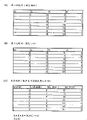
Then, use Figure 11 (A)~Figure 12 (C) that the advantage of comparing the present embodiment method with first, second comparative example is described.Figure 11 (A)~(C) is the bag width (highway width) that is provided with the packed data of Fig. 8 example when being 8 (I=1), and Figure 12 (A)~(C) is the bag width that is provided with the packed data of Fig. 9 example when being 16 (I=2).
And in Figure 11 (A)~Figure 12 (C), N is the byte number or the number of words of packed data, and L is the figure place of redundant data (pseudo-data).In addition, K is the figure place of input data, and M is the number that (K+L) bit data is arranged in the packed data.
In order to carry out format conversion, need count Figure 11 (A)~N, M of Figure 12 (C), the counter of K (byte counter, digit counter etc.) respectively.At this, identical for K condition in first, second comparative example and present embodiment.Thereby the counting counter of N, M and multipath transmission and decoding influence circuit scale from the circuit of the count value of counter etc.Thereby,, need make N * M as far as possible little in order to cut down circuit scale.In addition, the number of combinations of N/M is equivalent to the circuit number.
On the other hand, in order to reduce the volume of transmitted data of universal serial bus, be necessary to make the figure place L of redundant data to reduce.
Thereby,, preferably can realize minimizing of the minimizing of N * M, L simultaneously for the reduction that realizes volume of transmitted data simultaneously and the small-scaleization of circuit.
This point is fixed M in first comparative example of Figure 11 (A), Figure 12 (A), makes M=1.Thereby N * M (circuit scale) can diminish.For example, when calculating the summation of N * M, in Figure 11 (A) 12 points, in Figure 12 (A) 8 points.
But in this first comparative example, the figure place L of redundant data (volume of transmitted data) will become big.For example, when calculating the summation of L, in Figure 11 (A), be 13, in Figure 12 (A), be 45, become very big.
In addition, in second comparative example of Figure 11 (B), Figure 12 (B), L is fixed, make L=0.Thereby L (volume of transmitted data) can diminish.For example, when calculating the total of L, in Figure 11 (B), Figure 12 (B), it all is 0.
But, in this second comparative example, because N and M are big, so N * M (circuit scale) will become big.For example, when calculating the summation of N * M, in Figure 11 (B) 100 points, in Figure 12 (B), be 197 points, become very big.
Relative therewith, in the method for the present embodiment of Figure 11 (C), Figure 12 (C), L, M are set changeably according to K.That is, make L, M become suitable value according to K.
More particularly, in Figure 11 of I=1 (C), generate following packed data:
(1) when K=6, L=0, M=4, N=3
(2) when K=7, L=1, M=2, N=2
(3) when K=8, L=0, M=2, N=2
(4) when K=10, L=2, M=2, N=3
(5) when K=12, L=0, M=2, N=3
(6) when K=16, L=0, M=1, N=2 or
(7) when K=24, L=0, M=1, N=3.
In addition, in Figure 12 of I=2 (C), generate following packed data:
(11) when K=6, I=2, L=0, M=8, N=3
(12) when K=7, I=2, L=1, M=4, N=2
(13) when K=8, I=2, L=0, M=4, N=2
(14) when K=10, I=2, L=1, M=3, N=2
(15) when K=12, I=2, L=0, M=4, N=3
(16) when K=16, I=2, L=0, M=2, N=2 or
(17) when K=24, I=2, L=0, M=2, N=3.
At this moment, in the method for present embodiment, formula N * 8 * I=(K+L) * M sets up.For example, in Figure 11 of I=1 (C), formula N * 8=(K+L) * M sets up.In addition, in Figure 12 of I=2 (C), formula N * 8 * 2=(K+L) * M sets up.But the situation (situations of above-mentioned (14)) of having only the K=10 of Figure 12 (C) is an exception.
In addition, even can not satisfy the whole of above-mentioned (1)~(7), (11)~(17), also can only generate the packed data of a part that satisfies (1)~(7), (11)~(17).That is, also can only support a part of form of YUV 422, YUV 420, RGB 888, RGB565, RGB 444, RAW 6, RAW 7, RAW 8, RAW 10, RAW 12, JPEG8.
According to the method for above-mentioned present embodiment, as from Figure 11 (C), Figure 12 (C) can be clear and definite, N * M (circuit scale) can be reduced to less than second comparative example.For example, when calculating the summation of N * M, in Figure 11 (C) 37 points, in Figure 12 (C) 68 points.Thereby, be that 100 points, 197 second comparative example are compared with the summation of N * M, can fully reduce circuit scale.
In addition, in the method for present embodiment, the figure place of redundant data is lacked than first comparative example, and therefore, L (volume of transmitted data) also can reduce.For example, when calculating the summation of L, in Figure 11 (C) 3 points, 2 points in Figure 12 (C).Thereby, be that 13,45 first comparative example is compared with the summation of L, can fully reduce volume of transmitted data.
Thus, according to the method for present embodiment, can realize minimizing of N * M and minimizing of L simultaneously.Thereby, can not increase circuit scale significantly, can realize the serial transmission efficiently of multiple formatted data.
5. based on the data transfer mode of differential wave
Use Figure 13 that the serial transmission method of present embodiment is described below.In Figure 13, DTO+, DTO-are the data (OUT data) that host computer side (data transfer controller 10) outputs to target side (data transfer controller 30).CLK+, CLK-are the clock signals that host computer side offers target side.Host computer side and CLK+/-edge (for example is a rising edge.Also can be negative edge) synchronously, output DTO+/-.Thereby, target side can use CLK+/-sample and catch DTO+/-.Also have, in Figure 13, the clock signal clk that the target side basis is supplied with from host computer side+/-action.That is, CLK+/-become the clock signal of system of target side.Therefore, PLL (Phase Locked Loop) circuit 12 (broadly being meant clock signal generating circuit) is arranged on host computer side, is not arranged on target side.
DTI+, DTI-are the data (IN data) that target side outputs to host computer side.STB+, STB-are the gating signals (broadly being clock signal) that target side is supplied with host computer side.The CLK+ that the target side basis is supplied with from host computer side/-generation STB+/-and output.And, target side and STB+/-the edge (for example be rising edge.Also can be negative edge) synchronously, output DTI+/-.Thereby, host computer side can use STB+/-sample and catch DTI+/-.
DTO+/-, CLK+/-, DTI+/-, STB+/-each signal is that transmitter circuit (drive circuit) sends by for example current drives (perhaps driven) differential signal line corresponding with each signal of these signals (Differential Signal Lines).In addition, in order to realize more transmission at a high speed, also can be provided with DTO+ more than or equal to two couples/-, DTI+/-each differential signal line.
The transceiver 20 of host computer side comprises: OUT transmission is transmitted with (broadly be clock signal transmit use) acceptor circuit 28 with (broadly be data transmission with) acceptor circuit 26, gating with transmitter circuit 24, IN transmission with (broadly be data transmission with) transmitter circuit 22 and clock signal transmission.The transceiver 40 of target side comprises: the OUT transmission is transmitted with acceptor circuit 44, IN with acceptor circuit 42 and clock signal and is transmitted with transmitter circuit 46 and gating transmission transmitter circuit 48.In addition, also can be the formation that does not comprise the part of these circuit modules.
OUT transmission with transmitter circuit 22 and clock signal transmission with transmitter circuit 24 respectively by current drives DTO+/-, CLK+/-differential signal line, send DTO+/-, CLK+/-.OUT transmission with acceptor circuit 42 and clock signal transmission with acceptor circuit 44 respectively basis flow through DTO+/-, CLK+/-the electric current of differential signal line carry out the current/voltage conversion and the comparison process (differential processing and amplifying) of the differential voltage signal (first, second voltage signal) that carries out obtaining by electric current, voltage transformation, thereby reception DTO+/-, CLK+/-.
IN transmission with transmitter circuit 46 and clock signal transmission with transmitter circuit 48 respectively by current drives DTI+/-, STB+/-differential signal line, send DTI+/-, STB+/-.IN transmission with acceptor circuit 26 and gating transmission with acceptor circuit 28 respectively basis flow through DTI+/-, STB+/-the electric current of differential signal line carry out the current/voltage conversion and the comparison process (differential processing and amplifying) of the differential voltage signal (first, second voltage signal) that carries out obtaining by the current/voltage conversion, thereby reception DTI+/-, STB+/-.
6. electronic equipment
Figure 14 represents the configuration example of the electronic equipment of present embodiment.This electronic equipment comprises the data transfer controller 502,512,514,520,530 that illustrates in the present embodiment.In addition, comprise baseband engine 500 (broadly being communicator), application engine 510 (broadly being processor), camera 540 (broadly being camera head) or LCD 550 (broadly being display device).In addition, also can be the formation of omitting these a part.According to this formation, can realize portable phone that has camera-enabled and LCD (Liquid Crystal Dispaly) Presentation Function etc.But the electronic equipment of present embodiment is not limited to portable phone, can also be applied to various electronic equipments such as digital camera, PDA, electronic notebook, electronic dictionary or portable type information terminal.
As shown in figure 14, at the data transfer controller 502 that is arranged on the host computer side on the baseband engine 500 and be arranged between the data transfer controller 512 of the target side on the application engine 510 (graphics engine), carry out the serial transmission that illustrates in the present embodiment.In addition, between data transfer controller 514 that is arranged on the host computer side on the application engine 510 and the data transfer controller 520 that comprises camera interface circuits 522 or and comprise between the data transfer controller 530 of LCD interface circuit 532, also can carry out the serial transmission that illustrates in the present embodiment.In addition, also can realize baseband engine 500 and application engine 510 by identical hardware (CPU etc.).
According to the formation of Figure 14, compare with existing electronic equipment, can reduce the EMI noise.In addition, by small-scaleization, energy-conservationization of realization data transfer controller, thus further energy-conservationization of realization electronic equipment.In addition, when electronic equipment is portable phone, the signal wire that leads to the bonding pad (hinge area) of portable phone serial signal line can be made as, the summary of installing can be realized.
In addition, describe present embodiment as mentioned above in detail, but can not break away from a plurality of distortion of entity according to novel point of the present invention and effect, those skilled in the art can be apparent.Thereby such variation all is included in protection scope of the present invention.For example, in instructions or accompanying drawing, at least once the term that occurs together with different terms of broad sense or synonym (device, I byte etc.) more (camera, display device, 8/16 etc.) at random can enough be replaced as different terms with it at instructions or accompanying drawing.
In addition, the formation of data transfer controller or electronic equipment or action also are not limited to formation or the action that illustrates in the present embodiment, can carry out various distortion and implement.In addition, format conversion method is also unqualified in the method for explanations such as Fig. 8, Figure 12 (C).For example, K is not limited to 6,7,8,10,12,16,24 yet, and I is not limited to 1,2 yet.In addition, also can use method of the present invention in the format conversion outside the camera data.
Description of reference numerals
5: host apparatus 6: display driver
7: display floater 8: camera
10: data transfer controller (host computer side) 20: transceiver
30: data transfer controller (target side) 40: transceiver
90,100: link controller 92,110: interface circuit
200: data formatter 202: data buffer
204: pseudo-data deletion circuit 210: digit counter
212: byte counter 230: the bag buffer
240: bag parser circuitry 242: header sampling circuit
250: internal register 252:PCS register
254:PW register 300: data formatter
302: data buffer 304: pseudo-data insertion circuit
310: digit counter 312: byte counter
320: bag generative circuit 322: header generative circuit
330: bag impact damper 350: internal register
352:PCS register 354:PW register
Claims (14)
1. a data transfer controller is used for control data transmission, it is characterized in that, comprising:
Interface circuit, being transfused to a data unit by interface bus is the data of K position, wherein, K is the integer more than or equal to 2; And
Link controller is used to generate the bag that sends by universal serial bus,
Wherein, described link controller comprises:
Data formatter, be used for generating contain M (K+L) bit data (the byte packed data of N * I), described (K+L) bit data are by obtaining the pseudo-data in the additional L position of the described data of K position, wherein, M, N, I are the integers more than or equal to 1, and L is the integer more than or equal to 0; And
The bag generative circuit is used for generating the bag that data field is inserted with described packed data, as the bag that sends by described universal serial bus,
Described data formatter generates the described packed data that described L and M are set changeably according to described K.
2. data transfer controller according to claim 1 is characterized in that:
Described data formatter generates following packed data:
When K=6, I=1, L=0, M=4, N=3, perhaps
When K=7, I=1, L=1, M=2, N=2, perhaps
When K=8, I=1, L=0, M=2, N=2, perhaps
When K=10, I=1, L=2, M=2, N=3, perhaps
When K=12, I=1, L=0, M=2, N=3, perhaps
When K=16, I=1, L=0, M=1, N=2, perhaps
When K=24, I=1, L=0, M=1, N=3.
3. data transfer controller according to claim 1 is characterized in that:
Described data formatter generates following packed data:
When K=6, I=2, L=0, M=8, N=3, perhaps
When K=7, I=2, L=1, M=4, N=2, perhaps
When K=8, I=2, L=0, M=4, N=2, perhaps
When K=10, I=2, L=1, M=3, N=2, perhaps
When K=12, I=2, L=0, M=4, N=3, perhaps
When K=16, I=2, L=0, M=2, N=2, perhaps
When K=24, I=2, L=0, M=2, N=3.
4. data transfer controller according to claim 1 is characterized in that:
N×8×I=(K+L)×M
5. according to each described data transfer controller in the claim 1 to 4, it is characterized in that:
Described bag generative circuit inserts the configuration information that is used to be provided with described M, N in the header of the bag that sends by described universal serial bus.
6. according to each described data transfer controller in the claim 1 to 4, it is characterized in that, also comprise:
Internal register, storage is used to be provided with the configuration information of described M, N,
Wherein, described data formatter is inserted described pseudo-data according to described configuration information.
7. an electronic equipment is characterized in that, comprising:
Each described data transfer controller in the claim 1 to 4; And
The one or more devices that are connected with described data transfer controller by described interface bus.
8. a data transfer controller is used for control data transmission, it is characterized in that, comprising:
Interface circuit carries out data transfer controller and handles by the interface that system bus is connected between the host apparatus on the data transfer controller; And link controller, the bag that receives by universal serial bus to be resolved, the data that are the K position with a data unit output to described interface circuit, and wherein, K is the integer more than or equal to 2,
In the data field of the bag that receives by described universal serial bus, be inserted with (the data of byte of N * I) that contain M (K+L) bit data, it is described that (N * I) data of byte are the packed datas that described L and M are set changeably according to described K, wherein, the data of described (K+L) position are by obtaining the pseudo-data in the additional L position of the described data of K position, M, N, I are the integers more than or equal to 1, L is the integer more than or equal to 0
Described link controller comprises data formatter, and described data formatter is extracted the described data of K position out from described packed data, output in the described interface circuit.
9. data transfer controller according to claim 8 is characterized in that:
The described packed data that is inserted into bag is following data:
When K=6, I=1, L=0, M=4, N=3, perhaps
When K=7, I=1, L=1, M=2, N=2, perhaps
When K=8, I=1, L=0, M=2, N=2, perhaps
When K=10, I=1, L=2, M=2, N=3, perhaps
When K=12, I=1, L=0, M=2, N=3, perhaps
When K=16, I=1, L=0, M=1, N=2, perhaps
When K=24, I=1, L=0, M=1, N=3.
10. data transfer controller according to claim 8 is characterized in that:
The described packed data that is inserted into bag is following data:
When K=6, I=2, L=0, M=8, N=3, perhaps
When K=7, I=2, L=1, M=4, N=2, perhaps
When K=8, I=2, L=0, M=4, N=2, perhaps
When K=10, I=2, L=1, M=3, N=2, perhaps
When K=12, I=2, L=0, M=4, N=3, perhaps
When K=16, I=2, L=0, M=2, N=2, perhaps
When K=24, I=2, L=0, M=2, N=3.
11. data transfer controller according to claim 8 is characterized in that:
N×8×I=(K+L)×M
12. each described data transfer controller in 11 according to Claim 8 is characterized in that:
In the header of the bag that receives by described universal serial bus, be inserted with the configuration information that is used to be provided with described M, N,
Described link controller comprises the bag parser circuitry, and described bag parser circuitry is resolved the header of the bag that receives, and extracts described configuration information out from the header of bag,
Described data formatter is extracted the described data of K position out according to described configuration information from described packed data.
13. each described data transfer controller in 11 according to Claim 8 is characterized in that:
In the header of the bag that receives by described universal serial bus, be inserted with the configuration information that is used to be provided with described M, N,
Described link controller comprises the bag parser circuitry, and described bag parser circuitry is resolved the header of the bag that receives, and extracts described configuration information out from the header of bag,
Described data formatter is deleted described pseudo-data according to described configuration information.
14. an electronic equipment is characterized in that, comprising:
Each described data transfer controller in the claim 8 to 11; And
Be connected in described host apparatus on the described data transfer controller by described system bus.
Applications Claiming Priority (3)
| Application Number | Priority Date | Filing Date | Title |
|---|---|---|---|
| JP2005-086187 | 2005-03-24 | ||
| JP2005086187 | 2005-03-24 | ||
| JP2005086187A JP4207912B2 (en) | 2005-03-24 | 2005-03-24 | Data transfer control device and electronic device |
Publications (2)
| Publication Number | Publication Date |
|---|---|
| CN1838101A CN1838101A (en) | 2006-09-27 |
| CN100432974C true CN100432974C (en) | 2008-11-12 |
Family
ID=36741429
Family Applications (1)
| Application Number | Title | Priority Date | Filing Date |
|---|---|---|---|
| CNB2006100653944A Expired - Fee Related CN100432974C (en) | 2005-03-24 | 2006-03-23 | Data transfer control device and electronic instrument |
Country Status (7)
| Country | Link |
|---|---|
| US (1) | US7693086B2 (en) |
| EP (1) | EP1705577B1 (en) |
| JP (1) | JP4207912B2 (en) |
| KR (1) | KR100799399B1 (en) |
| CN (1) | CN100432974C (en) |
| DE (1) | DE602006001229D1 (en) |
| TW (1) | TWI322378B (en) |
Families Citing this family (21)
| Publication number | Priority date | Publication date | Assignee | Title |
|---|---|---|---|---|
| JP4075898B2 (en) * | 2005-03-23 | 2008-04-16 | セイコーエプソン株式会社 | Data transfer control device and electronic device |
| JP4186940B2 (en) | 2005-03-23 | 2008-11-26 | セイコーエプソン株式会社 | Data transfer control device and electronic device |
| JP2006268260A (en) * | 2005-03-23 | 2006-10-05 | Seiko Epson Corp | Data transfer controller and electronic equipment |
| JP4479703B2 (en) * | 2006-08-29 | 2010-06-09 | ブラザー工業株式会社 | Communication system and management device |
| JP4305481B2 (en) * | 2006-08-29 | 2009-07-29 | ブラザー工業株式会社 | Communication system, management device and information processing device |
| EP1988713A1 (en) * | 2007-04-30 | 2008-11-05 | STMicroelectronics (Research & Development) Limited | Image processing apparatus and method using padding data |
| JP5403995B2 (en) | 2007-12-10 | 2014-01-29 | キヤノン株式会社 | Signal transmission system and signal conversion circuit |
| WO2009075372A1 (en) * | 2007-12-10 | 2009-06-18 | Canon Kabushiki Kaisha | Signal transmission system and signal conversion circuit |
| CN103620573B (en) | 2011-04-06 | 2018-06-19 | 罗伯特·博世有限公司 | For matching the method and apparatus of the data transmission security in serial bus system |
| RU2620989C2 (en) * | 2011-04-06 | 2017-05-30 | Роберт Бош Гмбх | Method and apparatus for increasing throughput capacity in data transmission in serial bus system |
| WO2012146631A1 (en) | 2011-04-26 | 2012-11-01 | Robert Bosch Gmbh | Method and device for serial data transmission which is adapted to memory sizes |
| EP2726999B1 (en) | 2011-06-29 | 2015-09-09 | Robert Bosch GmbH | Method and device for serial data transmission having a flexible message size and a variable bit length |
| JPWO2013124915A1 (en) | 2012-02-24 | 2015-05-21 | パナソニックIpマネジメント株式会社 | Slave device, master device, and communication system |
| US9372692B2 (en) * | 2012-12-29 | 2016-06-21 | Intel Corporation | Methods, apparatus, instructions, and logic to provide permute controls with leading zero count functionality |
| JP5853211B2 (en) * | 2013-01-25 | 2016-02-09 | パナソニックIpマネジメント株式会社 | Bus interface device, relay device, and bus system including them |
| JP6398241B2 (en) | 2014-03-20 | 2018-10-03 | 富士ゼロックス株式会社 | Packet generating apparatus and program |
| CN105139812B (en) * | 2014-05-27 | 2018-01-30 | 奇景光电股份有限公司 | Data transmit and method of reseptance and data transmission system |
| CN105704063B (en) * | 2014-11-28 | 2018-09-07 | 奇点新源国际技术开发(北京)有限公司 | Information transferring method and device applied to car-mounted terminal |
| EP3419005A1 (en) * | 2017-06-22 | 2018-12-26 | Gemalto Sa | Computing device processing expanded data |
| US11436010B2 (en) | 2017-06-30 | 2022-09-06 | Intel Corporation | Method and apparatus for vectorizing indirect update loops |
| CN111061671B (en) * | 2019-12-13 | 2021-08-17 | 上海灵动微电子股份有限公司 | SPI transmission control method, sending equipment and receiving equipment |
Citations (7)
| Publication number | Priority date | Publication date | Assignee | Title |
|---|---|---|---|---|
| CN1296347A (en) * | 1999-01-26 | 2001-05-23 | 三星电子株式会社 | TDM multibus synchronous circuit and protocol, and operation method |
| CN1310531A (en) * | 2000-02-23 | 2001-08-29 | 华为技术有限公司 | Error detection method for high speed data transmission |
| CN1316698A (en) * | 2001-06-01 | 2001-10-10 | 北京四方同创保护与控制设备有限公司 | Software interface method for datal link layer in generalized asynchronous serial communication protocol. |
| US20020059488A1 (en) * | 2000-10-31 | 2002-05-16 | Seiko Epson Corporation | Data transfer control device and electronic instrument |
| EP1389761A2 (en) * | 2002-08-05 | 2004-02-18 | Seiko Epson Corporation | Data transfer control system, program and data transfer control method |
| US20040059965A1 (en) * | 2002-08-06 | 2004-03-25 | Network Equipment Technologies, Inc. | Synchronous serial data communication bus |
| US20040225810A1 (en) * | 2000-06-12 | 2004-11-11 | Shinji Hiratsuka | Serial bus data control device |
Family Cites Families (16)
| Publication number | Priority date | Publication date | Assignee | Title |
|---|---|---|---|---|
| JP2869092B2 (en) * | 1989-08-21 | 1999-03-10 | 日本電信電話株式会社 | Fixed length packetization method |
| US5694143A (en) * | 1994-06-02 | 1997-12-02 | Accelerix Limited | Single chip frame buffer and graphics accelerator |
| JP3622451B2 (en) * | 1997-10-03 | 2005-02-23 | ソニー株式会社 | Data processing apparatus, data processing method, and recording medium |
| JPH11161466A (en) * | 1997-11-27 | 1999-06-18 | Ricoh Co Ltd | Data transfer controller |
| US6157972A (en) * | 1997-12-05 | 2000-12-05 | Texas Instruments Incorporated | Apparatus and method for processing packetized information over a serial bus |
| JP3540154B2 (en) * | 1998-05-20 | 2004-07-07 | 三菱電機株式会社 | Multiplexing transmission device and multiplexing transmission method |
| JP4058888B2 (en) * | 1999-11-29 | 2008-03-12 | セイコーエプソン株式会社 | RAM built-in driver and display unit and electronic device using the same |
| JP2003141059A (en) * | 2001-11-02 | 2003-05-16 | Sony Corp | Information processor and method, storage medium and program |
| JP2003272359A (en) * | 2002-03-15 | 2003-09-26 | Canon Inc | Method for editing video data |
| JP3844072B2 (en) * | 2002-07-25 | 2006-11-08 | セイコーエプソン株式会社 | Semiconductor integrated circuit device, microcomputer and electronic device |
| JP2004110876A (en) * | 2002-09-13 | 2004-04-08 | Canon Inc | Coding rate controlling method of video data |
| JP2004139431A (en) * | 2002-10-18 | 2004-05-13 | Seiko Epson Corp | Method and device for controlling data transfer and display device |
| JP2004310963A (en) * | 2003-04-10 | 2004-11-04 | Canon Inc | Information recording method and its device |
| JP4186940B2 (en) | 2005-03-23 | 2008-11-26 | セイコーエプソン株式会社 | Data transfer control device and electronic device |
| JP2006268260A (en) | 2005-03-23 | 2006-10-05 | Seiko Epson Corp | Data transfer controller and electronic equipment |
| JP4075898B2 (en) | 2005-03-23 | 2008-04-16 | セイコーエプソン株式会社 | Data transfer control device and electronic device |
-
2005
- 2005-03-24 JP JP2005086187A patent/JP4207912B2/en not_active Expired - Fee Related
-
2006
- 2006-03-20 US US11/378,234 patent/US7693086B2/en not_active Expired - Fee Related
- 2006-03-22 TW TW95109755A patent/TWI322378B/en not_active IP Right Cessation
- 2006-03-23 CN CNB2006100653944A patent/CN100432974C/en not_active Expired - Fee Related
- 2006-03-23 KR KR20060026444A patent/KR100799399B1/en not_active IP Right Cessation
- 2006-03-23 DE DE200660001229 patent/DE602006001229D1/en active Active
- 2006-03-23 EP EP20060005956 patent/EP1705577B1/en not_active Expired - Fee Related
Patent Citations (7)
| Publication number | Priority date | Publication date | Assignee | Title |
|---|---|---|---|---|
| CN1296347A (en) * | 1999-01-26 | 2001-05-23 | 三星电子株式会社 | TDM multibus synchronous circuit and protocol, and operation method |
| CN1310531A (en) * | 2000-02-23 | 2001-08-29 | 华为技术有限公司 | Error detection method for high speed data transmission |
| US20040225810A1 (en) * | 2000-06-12 | 2004-11-11 | Shinji Hiratsuka | Serial bus data control device |
| US20020059488A1 (en) * | 2000-10-31 | 2002-05-16 | Seiko Epson Corporation | Data transfer control device and electronic instrument |
| CN1316698A (en) * | 2001-06-01 | 2001-10-10 | 北京四方同创保护与控制设备有限公司 | Software interface method for datal link layer in generalized asynchronous serial communication protocol. |
| EP1389761A2 (en) * | 2002-08-05 | 2004-02-18 | Seiko Epson Corporation | Data transfer control system, program and data transfer control method |
| US20040059965A1 (en) * | 2002-08-06 | 2004-03-25 | Network Equipment Technologies, Inc. | Synchronous serial data communication bus |
Also Published As
| Publication number | Publication date |
|---|---|
| KR100799399B1 (en) | 2008-01-30 |
| EP1705577A1 (en) | 2006-09-27 |
| TW200707282A (en) | 2007-02-16 |
| EP1705577B1 (en) | 2008-05-21 |
| DE602006001229D1 (en) | 2008-07-03 |
| US20060215703A1 (en) | 2006-09-28 |
| JP4207912B2 (en) | 2009-01-14 |
| US7693086B2 (en) | 2010-04-06 |
| JP2006268483A (en) | 2006-10-05 |
| KR20060103168A (en) | 2006-09-28 |
| TWI322378B (en) | 2010-03-21 |
| CN1838101A (en) | 2006-09-27 |
Similar Documents
| Publication | Publication Date | Title |
|---|---|---|
| CN100432974C (en) | Data transfer control device and electronic instrument | |
| CN100386718C (en) | Data transfer control device and electronic instrument | |
| KR101497001B1 (en) | Graphics multi-media ic and method of its operation | |
| JP3786120B2 (en) | Data transfer control device and electronic device | |
| US8127056B2 (en) | Data transfer control device including a switch circuit that switches write destination of received packets | |
| JPWO2008053858A1 (en) | Interface device and electronic device | |
| JP3835459B2 (en) | Data transfer control device and electronic device | |
| TW201319819A (en) | Method, computer readable medium and computing device for performing data transfers for serial ATA connections using data transfer rate throttling | |
| US20050201157A1 (en) | Data transfer control device and electronic instrument | |
| US7620762B2 (en) | Data transfer control device and electronic instrument | |
| US11902612B2 (en) | Video input port | |
| JP4924560B2 (en) | Data transfer control device and electronic device | |
| JP3780419B2 (en) | Data transfer control device and electronic device | |
| TW202306365A (en) | Method for data processing of frame receiving of an interconnection protocol and storage device | |
| JP4725541B2 (en) | Data transfer control device and electronic device | |
| JP4661810B2 (en) | Data transfer control device and electronic device | |
| US20240121326A1 (en) | Operation method for an electronic device and an electronic device capable of performing an advanced line coding | |
| JP2004234348A (en) | Data transfer control circuit, electronic device and data transfer control method |
Legal Events
| Date | Code | Title | Description |
|---|---|---|---|
| C06 | Publication | ||
| PB01 | Publication | ||
| C10 | Entry into substantive examination | ||
| SE01 | Entry into force of request for substantive examination | ||
| C14 | Grant of patent or utility model | ||
| GR01 | Patent grant | ||
| C17 | Cessation of patent right | ||
| CF01 | Termination of patent right due to non-payment of annual fee |
Granted publication date: 20081112 Termination date: 20130323 |