CN100423216C - Method for forming suspended transmission line structures in back end of line processing - Google Patents
Method for forming suspended transmission line structures in back end of line processing Download PDFInfo
- Publication number
- CN100423216C CN100423216C CNB2005800134522A CN200580013452A CN100423216C CN 100423216 C CN100423216 C CN 100423216C CN B2005800134522 A CNB2005800134522 A CN B2005800134522A CN 200580013452 A CN200580013452 A CN 200580013452A CN 100423216 C CN100423216 C CN 100423216C
- Authority
- CN
- China
- Prior art keywords
- transmission line
- signal transmssion
- line structure
- structure according
- dielectric layer
- Prior art date
- Legal status (The legal status is an assumption and is not a legal conclusion. Google has not performed a legal analysis and makes no representation as to the accuracy of the status listed.)
- Expired - Fee Related
Links
- 230000005540 biological transmission Effects 0.000 title claims abstract description 60
- 238000000034 method Methods 0.000 title abstract description 37
- 238000012545 processing Methods 0.000 title description 4
- 239000000463 material Substances 0.000 claims abstract description 57
- 238000001465 metallisation Methods 0.000 claims abstract description 21
- 239000004065 semiconductor Substances 0.000 claims abstract description 13
- 239000010410 layer Substances 0.000 claims description 46
- 239000004020 conductor Substances 0.000 claims description 17
- 239000011229 interlayer Substances 0.000 claims description 16
- 239000007769 metal material Substances 0.000 claims description 4
- 238000001020 plasma etching Methods 0.000 claims description 3
- 239000003989 dielectric material Substances 0.000 abstract description 10
- 230000008054 signal transmission Effects 0.000 abstract 4
- 230000008569 process Effects 0.000 description 16
- 229910052751 metal Inorganic materials 0.000 description 11
- 239000002184 metal Substances 0.000 description 11
- 230000004888 barrier function Effects 0.000 description 9
- 230000015572 biosynthetic process Effects 0.000 description 8
- 238000005530 etching Methods 0.000 description 7
- 238000007789 sealing Methods 0.000 description 6
- 238000000151 deposition Methods 0.000 description 5
- 230000008021 deposition Effects 0.000 description 5
- 238000005538 encapsulation Methods 0.000 description 5
- 238000005516 engineering process Methods 0.000 description 5
- 238000004519 manufacturing process Methods 0.000 description 5
- 239000011159 matrix material Substances 0.000 description 5
- 229910004298 SiO 2 Inorganic materials 0.000 description 4
- QVGXLLKOCUKJST-UHFFFAOYSA-N atomic oxygen Chemical compound [O] QVGXLLKOCUKJST-UHFFFAOYSA-N 0.000 description 4
- 229910052760 oxygen Inorganic materials 0.000 description 4
- 239000001301 oxygen Substances 0.000 description 4
- 229920000636 poly(norbornene) polymer Polymers 0.000 description 4
- RYGMFSIKBFXOCR-UHFFFAOYSA-N Copper Chemical compound [Cu] RYGMFSIKBFXOCR-UHFFFAOYSA-N 0.000 description 3
- XUIMIQQOPSSXEZ-UHFFFAOYSA-N Silicon Chemical compound [Si] XUIMIQQOPSSXEZ-UHFFFAOYSA-N 0.000 description 3
- 229910052802 copper Inorganic materials 0.000 description 3
- 239000010949 copper Substances 0.000 description 3
- 238000013461 design Methods 0.000 description 3
- 229910003460 diamond Inorganic materials 0.000 description 3
- 239000010432 diamond Substances 0.000 description 3
- 239000007789 gas Substances 0.000 description 3
- 229920000642 polymer Polymers 0.000 description 3
- 239000010703 silicon Substances 0.000 description 3
- 229910052710 silicon Inorganic materials 0.000 description 3
- FYGHSUNMUKGBRK-UHFFFAOYSA-N 1,2,3-trimethylbenzene Chemical compound CC1=CC=CC(C)=C1C FYGHSUNMUKGBRK-UHFFFAOYSA-N 0.000 description 2
- OKTJSMMVPCPJKN-UHFFFAOYSA-N Carbon Chemical compound [C] OKTJSMMVPCPJKN-UHFFFAOYSA-N 0.000 description 2
- MHAJPDPJQMAIIY-UHFFFAOYSA-N Hydrogen peroxide Chemical compound OO MHAJPDPJQMAIIY-UHFFFAOYSA-N 0.000 description 2
- 239000004642 Polyimide Substances 0.000 description 2
- VYPSYNLAJGMNEJ-UHFFFAOYSA-N Silicium dioxide Chemical compound O=[Si]=O VYPSYNLAJGMNEJ-UHFFFAOYSA-N 0.000 description 2
- 230000008901 benefit Effects 0.000 description 2
- 229910052799 carbon Inorganic materials 0.000 description 2
- 230000008878 coupling Effects 0.000 description 2
- 238000010168 coupling process Methods 0.000 description 2
- 238000005859 coupling reaction Methods 0.000 description 2
- 230000005611 electricity Effects 0.000 description 2
- 239000010931 gold Substances 0.000 description 2
- 229910002804 graphite Inorganic materials 0.000 description 2
- 239000010439 graphite Substances 0.000 description 2
- 239000000203 mixture Substances 0.000 description 2
- 229920003223 poly(pyromellitimide-1,4-diphenyl ether) Polymers 0.000 description 2
- 229920001721 polyimide Polymers 0.000 description 2
- 230000007261 regionalization Effects 0.000 description 2
- 229910052715 tantalum Inorganic materials 0.000 description 2
- GUVRBAGPIYLISA-UHFFFAOYSA-N tantalum atom Chemical compound [Ta] GUVRBAGPIYLISA-UHFFFAOYSA-N 0.000 description 2
- MZLGASXMSKOWSE-UHFFFAOYSA-N tantalum nitride Chemical compound [Ta]#N MZLGASXMSKOWSE-UHFFFAOYSA-N 0.000 description 2
- YEJRWHAVMIAJKC-UHFFFAOYSA-N 4-Butyrolactone Chemical compound O=C1CCCO1 YEJRWHAVMIAJKC-UHFFFAOYSA-N 0.000 description 1
- QTBSBXVTEAMEQO-UHFFFAOYSA-M Acetate Chemical compound CC([O-])=O QTBSBXVTEAMEQO-UHFFFAOYSA-M 0.000 description 1
- UFHFLCQGNIYNRP-UHFFFAOYSA-N Hydrogen Chemical compound [H][H] UFHFLCQGNIYNRP-UHFFFAOYSA-N 0.000 description 1
- 229910052581 Si3N4 Inorganic materials 0.000 description 1
- 229910000577 Silicon-germanium Inorganic materials 0.000 description 1
- FEBFYWHXKVOHDI-UHFFFAOYSA-N [Co].[P][W] Chemical compound [Co].[P][W] FEBFYWHXKVOHDI-UHFFFAOYSA-N 0.000 description 1
- 239000000956 alloy Substances 0.000 description 1
- 229910045601 alloy Inorganic materials 0.000 description 1
- 239000004411 aluminium Substances 0.000 description 1
- 229910052782 aluminium Inorganic materials 0.000 description 1
- XAGFODPZIPBFFR-UHFFFAOYSA-N aluminium Chemical compound [Al] XAGFODPZIPBFFR-UHFFFAOYSA-N 0.000 description 1
- 229910003481 amorphous carbon Inorganic materials 0.000 description 1
- 238000013459 approach Methods 0.000 description 1
- 125000004429 atom Chemical group 0.000 description 1
- 150000001721 carbon Chemical group 0.000 description 1
- 239000011248 coating agent Substances 0.000 description 1
- 238000000576 coating method Methods 0.000 description 1
- 239000012141 concentrate Substances 0.000 description 1
- 238000005260 corrosion Methods 0.000 description 1
- 230000007797 corrosion Effects 0.000 description 1
- 230000002950 deficient Effects 0.000 description 1
- 230000001934 delay Effects 0.000 description 1
- 238000009792 diffusion process Methods 0.000 description 1
- 238000007599 discharging Methods 0.000 description 1
- 230000009977 dual effect Effects 0.000 description 1
- 238000007772 electroless plating Methods 0.000 description 1
- 238000009713 electroplating Methods 0.000 description 1
- 230000005496 eutectics Effects 0.000 description 1
- 238000011049 filling Methods 0.000 description 1
- 229920002313 fluoropolymer Polymers 0.000 description 1
- 239000004811 fluoropolymer Substances 0.000 description 1
- 239000011521 glass Substances 0.000 description 1
- PCHJSUWPFVWCPO-UHFFFAOYSA-N gold Chemical compound [Au] PCHJSUWPFVWCPO-UHFFFAOYSA-N 0.000 description 1
- 229910052737 gold Inorganic materials 0.000 description 1
- 238000000227 grinding Methods 0.000 description 1
- 229910052739 hydrogen Inorganic materials 0.000 description 1
- 239000001257 hydrogen Substances 0.000 description 1
- 229910044991 metal oxide Inorganic materials 0.000 description 1
- 150000004706 metal oxides Chemical class 0.000 description 1
- 238000004377 microelectronic Methods 0.000 description 1
- 238000012986 modification Methods 0.000 description 1
- 230000004048 modification Effects 0.000 description 1
- 150000004767 nitrides Chemical class 0.000 description 1
- 239000011368 organic material Substances 0.000 description 1
- 230000003647 oxidation Effects 0.000 description 1
- 238000007254 oxidation reaction Methods 0.000 description 1
- 230000003071 parasitic effect Effects 0.000 description 1
- 238000000206 photolithography Methods 0.000 description 1
- 229920002120 photoresistant polymer Polymers 0.000 description 1
- 238000007747 plating Methods 0.000 description 1
- 230000001681 protective effect Effects 0.000 description 1
- 230000009467 reduction Effects 0.000 description 1
- 239000011347 resin Substances 0.000 description 1
- 229920005989 resin Polymers 0.000 description 1
- 238000000926 separation method Methods 0.000 description 1
- 238000004904 shortening Methods 0.000 description 1
- 235000012239 silicon dioxide Nutrition 0.000 description 1
- 239000000377 silicon dioxide Substances 0.000 description 1
- HQVNEWCFYHHQES-UHFFFAOYSA-N silicon nitride Chemical compound N12[Si]34N5[Si]62N3[Si]51N64 HQVNEWCFYHHQES-UHFFFAOYSA-N 0.000 description 1
- 239000000126 substance Substances 0.000 description 1
- 239000000758 substrate Substances 0.000 description 1
- 238000012360 testing method Methods 0.000 description 1
- 238000005979 thermal decomposition reaction Methods 0.000 description 1
- 238000007669 thermal treatment Methods 0.000 description 1
- WFKWXMTUELFFGS-UHFFFAOYSA-N tungsten Chemical compound [W] WFKWXMTUELFFGS-UHFFFAOYSA-N 0.000 description 1
- 229910052721 tungsten Inorganic materials 0.000 description 1
- 239000010937 tungsten Substances 0.000 description 1
- XLYOFNOQVPJJNP-UHFFFAOYSA-N water Substances O XLYOFNOQVPJJNP-UHFFFAOYSA-N 0.000 description 1
Images


Classifications
-
- H—ELECTRICITY
- H01—ELECTRIC ELEMENTS
- H01L—SEMICONDUCTOR DEVICES NOT COVERED BY CLASS H10
- H01L27/00—Devices consisting of a plurality of semiconductor or other solid-state components formed in or on a common substrate
- H01L27/02—Devices consisting of a plurality of semiconductor or other solid-state components formed in or on a common substrate including semiconductor components specially adapted for rectifying, oscillating, amplifying or switching and having at least one potential-jump barrier or surface barrier; including integrated passive circuit elements with at least one potential-jump barrier or surface barrier
-
- H—ELECTRICITY
- H01—ELECTRIC ELEMENTS
- H01P—WAVEGUIDES; RESONATORS, LINES, OR OTHER DEVICES OF THE WAVEGUIDE TYPE
- H01P11/00—Apparatus or processes specially adapted for manufacturing waveguides or resonators, lines, or other devices of the waveguide type
- H01P11/001—Manufacturing waveguides or transmission lines of the waveguide type
- H01P11/003—Manufacturing lines with conductors on a substrate, e.g. strip lines, slot lines
-
- H—ELECTRICITY
- H01—ELECTRIC ELEMENTS
- H01L—SEMICONDUCTOR DEVICES NOT COVERED BY CLASS H10
- H01L21/00—Processes or apparatus adapted for the manufacture or treatment of semiconductor or solid state devices or of parts thereof
- H01L21/70—Manufacture or treatment of devices consisting of a plurality of solid state components formed in or on a common substrate or of parts thereof; Manufacture of integrated circuit devices or of parts thereof
- H01L21/71—Manufacture of specific parts of devices defined in group H01L21/70
- H01L21/768—Applying interconnections to be used for carrying current between separate components within a device comprising conductors and dielectrics
- H01L21/76801—Applying interconnections to be used for carrying current between separate components within a device comprising conductors and dielectrics characterised by the formation and the after-treatment of the dielectrics, e.g. smoothing
- H01L21/7682—Applying interconnections to be used for carrying current between separate components within a device comprising conductors and dielectrics characterised by the formation and the after-treatment of the dielectrics, e.g. smoothing the dielectric comprising air gaps
-
- H—ELECTRICITY
- H01—ELECTRIC ELEMENTS
- H01L—SEMICONDUCTOR DEVICES NOT COVERED BY CLASS H10
- H01L21/00—Processes or apparatus adapted for the manufacture or treatment of semiconductor or solid state devices or of parts thereof
- H01L21/70—Manufacture or treatment of devices consisting of a plurality of solid state components formed in or on a common substrate or of parts thereof; Manufacture of integrated circuit devices or of parts thereof
- H01L21/71—Manufacture of specific parts of devices defined in group H01L21/70
- H01L21/768—Applying interconnections to be used for carrying current between separate components within a device comprising conductors and dielectrics
- H01L21/76838—Applying interconnections to be used for carrying current between separate components within a device comprising conductors and dielectrics characterised by the formation and the after-treatment of the conductors
-
- H—ELECTRICITY
- H01—ELECTRIC ELEMENTS
- H01L—SEMICONDUCTOR DEVICES NOT COVERED BY CLASS H10
- H01L23/00—Details of semiconductor or other solid state devices
- H01L23/52—Arrangements for conducting electric current within the device in operation from one component to another, i.e. interconnections, e.g. wires, lead frames
- H01L23/522—Arrangements for conducting electric current within the device in operation from one component to another, i.e. interconnections, e.g. wires, lead frames including external interconnections consisting of a multilayer structure of conductive and insulating layers inseparably formed on the semiconductor body
- H01L23/5222—Capacitive arrangements or effects of, or between wiring layers
- H01L23/5225—Shielding layers formed together with wiring layers
-
- H—ELECTRICITY
- H01—ELECTRIC ELEMENTS
- H01L—SEMICONDUCTOR DEVICES NOT COVERED BY CLASS H10
- H01L2223/00—Details relating to semiconductor or other solid state devices covered by the group H01L23/00
- H01L2223/58—Structural electrical arrangements for semiconductor devices not otherwise provided for
- H01L2223/64—Impedance arrangements
- H01L2223/66—High-frequency adaptations
- H01L2223/6605—High-frequency electrical connections
- H01L2223/6616—Vertical connections, e.g. vias
- H01L2223/6622—Coaxial feed-throughs in active or passive substrates
-
- H—ELECTRICITY
- H01—ELECTRIC ELEMENTS
- H01L—SEMICONDUCTOR DEVICES NOT COVERED BY CLASS H10
- H01L2223/00—Details relating to semiconductor or other solid state devices covered by the group H01L23/00
- H01L2223/58—Structural electrical arrangements for semiconductor devices not otherwise provided for
- H01L2223/64—Impedance arrangements
- H01L2223/66—High-frequency adaptations
- H01L2223/6605—High-frequency electrical connections
- H01L2223/6627—Waveguides, e.g. microstrip line, strip line, coplanar line
-
- H—ELECTRICITY
- H01—ELECTRIC ELEMENTS
- H01L—SEMICONDUCTOR DEVICES NOT COVERED BY CLASS H10
- H01L23/00—Details of semiconductor or other solid state devices
- H01L23/52—Arrangements for conducting electric current within the device in operation from one component to another, i.e. interconnections, e.g. wires, lead frames
- H01L23/522—Arrangements for conducting electric current within the device in operation from one component to another, i.e. interconnections, e.g. wires, lead frames including external interconnections consisting of a multilayer structure of conductive and insulating layers inseparably formed on the semiconductor body
- H01L23/532—Arrangements for conducting electric current within the device in operation from one component to another, i.e. interconnections, e.g. wires, lead frames including external interconnections consisting of a multilayer structure of conductive and insulating layers inseparably formed on the semiconductor body characterised by the materials
- H01L23/53204—Conductive materials
- H01L23/53209—Conductive materials based on metals, e.g. alloys, metal silicides
- H01L23/53228—Conductive materials based on metals, e.g. alloys, metal silicides the principal metal being copper
- H01L23/53238—Additional layers associated with copper layers, e.g. adhesion, barrier, cladding layers
-
- H—ELECTRICITY
- H01—ELECTRIC ELEMENTS
- H01L—SEMICONDUCTOR DEVICES NOT COVERED BY CLASS H10
- H01L2924/00—Indexing scheme for arrangements or methods for connecting or disconnecting semiconductor or solid-state bodies as covered by H01L24/00
- H01L2924/0001—Technical content checked by a classifier
- H01L2924/0002—Not covered by any one of groups H01L24/00, H01L24/00 and H01L2224/00
-
- H—ELECTRICITY
- H01—ELECTRIC ELEMENTS
- H01L—SEMICONDUCTOR DEVICES NOT COVERED BY CLASS H10
- H01L2924/00—Indexing scheme for arrangements or methods for connecting or disconnecting semiconductor or solid-state bodies as covered by H01L24/00
- H01L2924/19—Details of hybrid assemblies other than the semiconductor or other solid state devices to be connected
- H01L2924/1901—Structure
- H01L2924/1903—Structure including wave guides
-
- H—ELECTRICITY
- H01—ELECTRIC ELEMENTS
- H01L—SEMICONDUCTOR DEVICES NOT COVERED BY CLASS H10
- H01L2924/00—Indexing scheme for arrangements or methods for connecting or disconnecting semiconductor or solid-state bodies as covered by H01L24/00
- H01L2924/30—Technical effects
- H01L2924/301—Electrical effects
- H01L2924/3011—Impedance
Abstract
A method for forming a transmission line structure (300) for a semiconductor device includes forming an interlevel dielectric layer over a first metallization level, removing a portion of the interlevel dielectric layer and forming a sacrificial material within one or more voids (308) created by the removal of the portion of the interlevel dielectric layer. A signal transmission line (302) is formed in a second metallization level formed over the interlevel dielectric layer, the signal transmission line (302) being disposed over the sacrificial material. A portion of dielectric material included within the second metallization level is removed so as to expose the sacrificial material, wherein a portion of the sacrificial material is exposed through a plurality of access holes (310) formed through the signal transmission line (302). The sacrificial material is removed so as to create an air gap beneath the signal transmission line (302).
Description
Technical field
The present invention relates generally to semiconductor fabrication process, relate in particular to the method that in handle the line rear end of semiconductor device (BEOL), forms suspended transmission line structure.
Background technology
Semiconductor integrated circuit is made by MOS (metal-oxide semiconductor (MOS)) or by the bipolar transistor at the top planar major surface place that is integrated in silicon usually.Between various transistor, and the electrical interconnection line of some transistor AND gate between the access pin around the chip taked two (or many) " aspect " interconnection line usually, that is, have along the form of the conductor wire of the metallization band forms on two (or a plurality of) substantially flat surfaces that are parallel to each other orientation and insulate by suitable insulating barrier mutually insulated and with the top flat surface of chip.In insulating barrier, according to required circuit interconnection, the place of wanting of what is the need in office is equipped with through-hole interconnection (window).
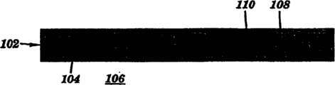
Especially, microstrip structure mainly is used in the not intensive radio frequency of wiring (RF) the CMOS/SiGe chip.In general, microstrip structure is reasonably well kept apart signal and following lossy base material.Shown in Fig. 1 (a), bottom ground plane 14 and the interlayer dielectric material between them (ILD) 16 that typical microstrip transmission line structure 10 comprises signal transmssion line 12, is used to shield.Therefore because shielding 14 and signal transmssion line 12 are manufactured into standard interconnect components, with dielectric material 16 they are sealed.The example of dielectric material comprises like this, for example, and silicon dioxide (SiO
2), SiCOH, SiLK, FSG, USG etc.The scope of the dielectric constant of dielectric material generally from about 2.5 to about 4.1 like this.
On the other hand, co-planar waveguide is used in the higher relatively place of wiring density usually, for example in the CMOS chip, is difficult to set up the place of tangible return path below holding wire.The sole mode of reliable inverse signal is also to use the arrange metal level identical with the metal level of arranging that is used for holding wire.Therefore, as Fig. 1 (b), typical coplanar waveguide transmission line structure 20 comprises signal transmssion line 22 and is in two adjacent shields lines 24 of same wiring aspect with transmission line 22.Coplanar waveguide structure 20 and silicon base 26 fixed distance.The third structure (that is the characteristic that, has little band and coplanar structure) that is called the microstrip transmission line that possesses the side shielding also has been used in the existing transmission line structure.
Shown in Fig. 1 (c), ground plane 34 and the interlayer dielectric material between them 36 that the typical microstrip transmission line structure 30 that exists side to shield comprises signal transmssion line 32, is used to shield.But described in addition shielding also comprises with signal transmssion line 32 and is in shielding conductor 38 on the same wiring layer.Shielding conductor 38 is contiguous with ground plane 34 electricity by the through hole 40 of conductive fill.The same with microstrip structure 10, traditional coplanar elements also fences up with the ILD material.
In each case, use the ILD material can to cause dielectric loss as described above and reduced the Q factor of transmission line in the BEOL interconnection.So, wish to set up the strip line structure that combines with advanced low-k materials, so that improve the performance of transmission line.
Summary of the invention
The shortcoming of above-mentioned prior art and defective overcome by a kind of method that forms the transmission line structure of semiconductor device or relax.In an one exemplary embodiment, this method comprises the interlayer dielectric layer that is formed on first metallization level; Remove a part of interlayer dielectric layer; With forming expendable material by removing in one or more spaces that a part of interlayer dielectric layer forms.Form signal transmssion line in second metallization level that forms on interlayer dielectric layer, signal transmssion line is on the expendable material.Remove a part of dielectric material that is included in second metallization level, so that expendable material is come out, wherein, a part of expendable material is to come out by several tunnel holes of passing signal transmssion line formation.Remove expendable material, so that below signal transmssion line, form air gap.
In another embodiment, the line rear end transmission line structure of semiconductor device comprises the interlayer dielectric layer that is formed on first metallization level; With the one or more spaces that are formed in the interlayer dielectric layer.Form signal transmssion line in second metallization level, this signal transmssion line is on one or more spaces.Signal transmssion line further comprises and passes wherein several tunnel holes that form, and with the passage of removing of the expendable material that is provided for limiting one or more spaces, wherein, one or more spaces limit the air gap below the signal transmssion lines.
In yet another embodiment, line rear end microstrip transmission line structure comprises and is formed on a signal transmssion line on the metallization level and is formed on ground plane on another metallization level.Air gap is between signal transmssion line and the ground plane, and this air gap forms in interlayer dielectric layer.One of signal transmssion line and ground plane further comprise and pass wherein several tunnel holes that form, with the passage of removing of the expendable material that is provided for limiting air gap.
In another embodiment, line rear end coplanar waveguide transmission line structure comprises the signal transmssion line that is formed on first metallization level; With a pair of coplane shielding conductor adjacent in first metallization level with signal transmssion line.Air gap is in below the signal transmssion line, and this air gap forms in interlayer dielectric layer.Signal transmssion line further comprises and passes wherein several tunnel holes that form, with the passage of removing of the expendable material that is provided for limiting air gap.
Description of drawings
The accompanying exemplary drawings of similar elements is numbered in reference with duplicate numbers in several accompanying drawings:
Fig. 1 (a) is the profile of traditional microstrip transmission line structure;
Fig. 1 (b) is the profile of conventional co-planar waveguide line structure;
Fig. 1 (c) is the profile that has traditional microstrip transmission line structure of side shielding;
Fig. 2 (a)-2 (i) be illustration according to embodiments of the invention, form the series of process flow chart of the method for suspended transmission line structure during online rear end (BEOL) handles;
Fig. 2 (j) is the design of the last suspended transmission line structure of formation in Fig. 2 (a)-2 (i) and plane (up and down) figure of mask layout;
Fig. 3 is the profile that contains the microstrip transmission line embodiment of air gap dielectric;
Fig. 4 is the profile that contains the inverted microstrip transmission line embodiment of air gap dielectric;
Fig. 5 contains the not profile of the coplanar transmission embodiment under holding wire of air gap dielectric and ground plane;
Fig. 6 contains air gap dielectric and without any the profile of the coplanar waveguide transmission line embodiment of bottom ground plane;
Fig. 7 (a)-7 (g) be illustration according to embodiments of the invention, seal the series of process flow chart of a kind of possibility method of the suspended transmission line structure as in Fig. 2 (a)-2 (g), forming;
Fig. 8 (a)-8 (d) be illustration according to embodiments of the invention, seal the series of process flow chart of a kind of alternative method of the suspended transmission line structure as in Fig. 2 (a)-2 (g), forming;
Fig. 9 (a)-9 (c) is illustrated in to contain air gap and have bottom and the series of process flow chart of the formation of the strip line transmission line embodiment of top layer ground plane below the holding wire; With
Figure 10 (a)-10 (d) be describe with little band air gap transmission line structure (for example as shown in Figure 3) with have a SiO
2The figure of various analog result that dielectric traditional microstrip structure is compared.
Embodiment
Herein disclosed is the method that forms suspended transmission line structure in the semiconductor processes of online rear end (BEOL), wherein, this Integrated Solution causes the low copper EEOL transmission line structure of dielectric loss.But, should be realized that method embodiment as herein described is not limited to such copper EEOL, can be generalized to other interconnection line that utilizes various materials to make, these materials comprise, for example, aluminium, tungsten, gold etc., but be not limited to these.In one embodiment, this integrated approach causes forming air gap between holding wire and ground plane, so that reduce the interconnection dielectric constant, therefore, is reduced in the value of the extra high capacitive cross-talk of possibility on the microwave frequency.In addition, hereinafter employed term " air gap " may not be confined to have air between holding wire and ground plane, also extends to description or refers to exist any gas phase material or vacuum.
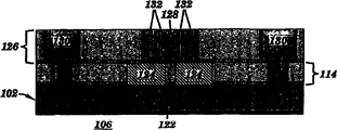
Prevailingly with reference to Fig. 2 (a)-2 (i), Fig. 2 shows illustration according to embodiments of the invention now, forms the series of process flow chart of the method for suspended transmission line structure during online rear end (BEOL) handles.From Fig. 2 (a), form ground plane 102 by single damascene process technique.Especially, gasket material 104 (for example, tantalum nitride/tantalum) is deposited in the opening that is formed in the insulating barrier 106, after this, BEOL metal 108 (for example, copper) is deposited on the gasket material, make it smooth then by (for example) plating, sputter etc.Shown in Fig. 2 (b), after this, fall a part of BEOL metal 108 by etchback, deposit other gasket material and make it the smooth liner part 110 that forms, fully ground plane 102 is sealed.Through so sealing, ground plane 102 just can be resisted the atom diffusion of metal 108, and resists the oxidation that subsequent processing steps hereinafter described causes.
In an one exemplary embodiment, the upper surface of wiring 108 falls in respect to the upper strata of dielectric layer 106. and a kind of method that metal is fallen in is to use the timing Wet-type etching to obtain desired depth.For example, using the solution of being made up of water, acetate and hydrogen peroxide (for example, being respectively the concentration of 3 liters, 15 milliliters and 9 milliliters) reaches about 2.5 minutes and just can obtain about 600 dusts
 To about 800 dusts
 The degree of depth.Then, deposition one
 deck barrier material 110, barrier material 110 is used for copper-clad is sealed, so that protect it during subsequent treatment.A specific embodiment comprises one deck 100
 Thick tantalum adds 400
 Tantalum nitride (TaN).Alternately,
 barrier material 110 also can by dielectric or arbitrarily other suitable metal barrier layer constitute.
Another method of encapsulated metal is the photoresist together with opposite polarity, is used to limit the same mask of conductor, and the surface from the top begins the etching barrier material then, forms the pattern of covering barrier layer 110.Other material that can be used to seal interconnection line comprises can be by electroplating and electroless plating, and cobalt-tungsten-phosphorus (CoWP) and nickel-Jin (Ni-Au) alloy of other method deposition.
Fig. 2 (c) illustration according to coplanar transmission embodiment formation through hole 112 in interlayer dielectric material (ILD) layer 114.ILD layer 114 can comprise, for example, and silicon nitride (Si
3N
4) layer 116, add the thicker SiO that after this forms pattern with photolithography for limited hole
2Layer 118.Subsequently, gasket material and metal material are formed in the opening and being flattened with the known method of prior art, to form the through hole 112 of filling.
With reference to Fig. 2 (d), in ILD layer 114, between through hole 112, form parallel groove 120.Alternately, can keep original nitride layer 116 at the place, bottom of groove 120, so that as discussed above, sealing and protective earthing face.Channel layout is become to form dielectric support 122 between them.Photoengraving pattern formation method in this step can be designed so that supporting member 122 is the continuous tracks along the length of ground plane 102, perhaps, alternately, supporting member is several discrete pillars of arranging along the length of ground plane 102.In other words, are corbelings if wish supporting member 122, so, groove 120 is along the length (that is, seeing toward the inside of figure) mutual " connection " on many positions of ground plane 102.It should further be appreciated that, also supporting member 122 can be configured to the discrete pillar of two or many parallel orbits or two or more series.Then, in Fig. 2 (e), in groove, form expendable material 124 and make it smooth.Expendable material 124 can be, for example, is chosen to subsequently the organic low k dielectric polymer that can be removed selectively with respect to ILD layer and BEOL metal material.
Can be as some exemplary materials of expendable material 124
 Diamond-like-carbon (DLC) and polynorbornene (PNB).
Be the semiconductor dielectric that Dow chemical company makes, can be used on picture Porous
In the various formation of such product.The fluoropolymer resin that this particular dielectric is made up of gamma-butyrolacton, special-purpose B rank polymer and trimethylbenzene.The another kind of material that can be used for this purpose is DLC, and it is the amorphous carbon that comprises coating that wherein a part of carbon atom is bonded together in the mode similar to diamond.The oxidizable material of short of exposure can be removed these materials by being exposed under the oxygen plasma.If have the oxidizable material that will during removing organic material, expose, then can use H
2/ CO
2/ CO/N
2The type plasma is removed technology.Those of ordinary skill in the art can be used for active-ion-etch with these admixture of gas.Polynorbornene is the sacrificial polymer in about 400-500 ℃ of thermal decomposition.Therefore, use simple thermal treatment and just can remove expendable material.
Diamond-like-carbon (DLC) and polynorbornene (PNB).
Be the semiconductor dielectric that Dow chemical company makes, can be used on picture Porous
In the various formation of such product.The fluoropolymer resin that this particular dielectric is made up of gamma-butyrolacton, special-purpose B rank polymer and trimethylbenzene.The another kind of material that can be used for this purpose is DLC, and it is the amorphous carbon that comprises coating that wherein a part of carbon atom is bonded together in the mode similar to diamond.The oxidizable material of short of exposure can be removed these materials by being exposed under the oxygen plasma.If have the oxidizable material that will during removing organic material, expose, then can use H
2/ CO
2/ CO/N
2The type plasma is removed technology.Those of ordinary skill in the art can be used for active-ion-etch with these admixture of gas.Polynorbornene is the sacrificial polymer in about 400-500 ℃ of thermal decomposition.Therefore, use simple thermal treatment and just can remove expendable material.
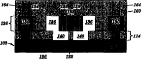
Fig. 2 (f) illustration the formation of signal level metallization structures.As shown in the figure, on ILD layer 114, form another dielectric layer 126, after this limit opening therein, so that form signal transmssion line 128 and coplane shielding conductor 130.But as can be seen, the pattern of signal transmssion line form to be what the mode with several connectors 132 that keep dielectric layer 126 realized.Therefore, when adding liner and metal material for coplane shielding conductor 130 and signal transmssion line 128, gained signal transmssion line metal is not totally continuous along its length.
The same with the situation of ground plane 102, etchback falls to be used for a part of BEOL metal of signal transmssion line 128 and coplane shielding conductor 130, gets ready for forming the last liner 134 of sealing signal level metallization structures in the above.This is presented among Fig. 2 (g).In Fig. 2 (h), realize that another pattern forms step, so that remove a part of dielectric layer 126 adjacent with each side of signal transmssion line 128, thus the space 136 that formation comes out the outward flange of expendable material 124.In addition, also remove the dielectric plugs 132 that after the pattern of signal transmssion line 128 forms, stays now, so that form tunnel holes 138.Shown in Fig. 2 (i), created condition and (for example, passed through O discharging expendable material 124 along being combined into of many Dian Chu space 136 of signal transmssion line and tunnel holes 138
2Plasma etching).
When selected expendable material 124 is
 Or during DLC, discharge selected
 expendable material 124 by being exposed under the oxygen that decomposes above-mentioned material or the hydrogen plasma.Article " corrosion of diamond thin and graphite in the oxygen plasma " (the A.Joshi and R.Nimmagadda that can deliver at A.Joshi and R.Nimmagadda about other details of this technology, " Erosionof diamond films and graphite in oxygen plasma ", Journal of MaterialResearch, Vol.6, No.7, p.1484,1996, published by the MaterialsResearch Society) finds in, for your guidance in this incorporated.For polynorbornene, can heat-treat with the release signal line at 425 ℃.Other details of this release process can be at people's such as Dhananjay Bhusari paper " manufacturing of the air passage structure of microfluid, micro electronmechanical and microelectronic applications " (Dhananjay Bhusari et al, " Fabrication ofAir-Channel Structures for Microfludic; Microelectromechanical; andMicroelectroinic Applications; Journal of MicroelectromechanicalSystems; Vol.10; No.3, p.400,2001) find in, for your guidance in this incorporated.So the transmission line structure of gained comprises two all low-k under signal transmssion line 128 (gas) cracks 140 in ILD layer 114, and in the signals layer with a pair of coplane shielding conductor 130 of signal transmssion line 128 adjacent (by space 136).
Fig. 2 (j) illustration the design of suspended transmission line structure and layout about (plane) figure.In the design of tunnel holes 138, special consideration has been made in the arrangement of aperture, so that create conditions for the reliable propagation of signal.In the embodiment of Fig. 2 (j), realized the layout of tunnel holes and conductor edge quadrature, so that make the current interference minimum.In addition, the size of tunnel holes 138 should be enough big, so that expendable material is fallen by lateral etches, but also should be enough little, so that make the increase minimum of holding wire resistance.
After having discharged expendable material, a kind of possibility method of sealing suspended transmission line structure is that deposition one deck polymide (polyimides) or kapton (polyimides) (not shown) are with complete covering device.Then, make further BEOL if necessary and handle, can make the polymide/kapton layer form pattern it is contacted with the test pad.
Fig. 7 (a)-7 (g) illustration can realize (beginning) and also can be used for describing alternative Processing Example how to seal suspended transmission line structure from the structure that among Fig. 2 (g), forms.In Fig. 7 (b), on signal line structure, deposited dielectric layer 142 (Si preferably
3N
4) and ILD layer 144 (SiO preferably
2).Shown in Fig. 7 (c), utilize photoengraving pattern formation (composition) and etching step above holding wire 128, to form cavity 146.During this cavity of etching, also near holding wire 128 and by the release aperture that is included in the holding wire 128, from cavity zone, remove dielectric material.
Subsequently, in Fig. 7 (d), the other releasable material 148 of usefulness (for example, is used as aforementioned
 Or DLC) fills etching region, make it smooth then.Reuse now and be in following same sacrificial material at first, so that dispose procedure is removed all layers of release material.Fig. 7 (e) illustration composition and etching adding through
 hole 154, another dielectric layer 152 on layer 150 (general designation of layer 142 and 144).Then, shown in Fig. 7 (f), in the final step of Integrated Solution, remove these through holes 154 that are used to provide the passage that arrives releasable material 148.At last, Fig. 7 (g) illustration last encapsulation step, this last encapsulation step relates to the deposition of another dielectric layer 158 of clamping (pinch off) small through hole 154, thereby seals up suspended transmission line structure airtightly.
Referring now to Fig. 8 (a)-8 (d), show another replacement method that begins to seal suspended transmission line structure from Fig. 2 (i), wherein, carrier matrix is used for this encapsulation process.This carrier matrix can comprise Al
2O
3, glass, silicon etc., but do not limit to these.Shown in Fig. 8 (b), deposition interlayer dielectric material 160 (for example, SiO on such carrier matrix 162
2).Then, shown in Fig. 8 (c), utilize as low-temperature bonding, any of many known standard technologies that the eutectic bonding is such combines carrier matrix 162 and suspended transmission line structure.
Then, can utilize any carrier matrix 162 of removing of the many technologies as Wet-type etching, plasma etching, complanation, grinding etc.Shown in Fig. 8 (d), under any circumstance, carrier removal process all should terminate on the ILD layer 160.After this encapsulation process, then can proceed standard BEOL and handle.
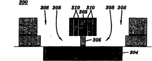
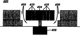
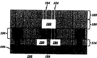
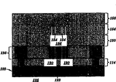
Should be realized that except the coplanar transmission structure with ground plane and air dielectric, said process also is applicable to the transmission line structure that forms other type.For example, Fig. 3 illustration comprise the microstrip transmission line embodiment 300 of the signal transmssion line of sealing 302, the ground plane of sealing 304 and supporting member 306.By to form the space at ILD layer and signal line layer, further form air gap dielectric to above-mentioned similar mode.Equally, signal transmssion line 302 includes and helps discharge expendable material interstitial several tunnel holes 310 on the ILD layer.Fig. 4 illustration inverted microstrip transmission line embodiment 400, wherein, on the metallization level lower, form signal transmssion line 402 than ground plane 404.So, for the space 408 that forms air gap dielectric, replace signal transmssion line 402, at first in ground plane 404, form tunnel holes.
With reference to Fig. 5, Fig. 5 shows another coplanar transmission embodiment 500, wherein, does not form ground plane under signal transmssion line 504. and replace, make coplane shielding conductor 506 electricity separation mutually, but each bar passes through through hole 510 and descends layer line 508 couplings separately.Fig. 6 shows coplanar waveguide structure 600, and wherein, ground plane only comprises two shielding conductors 606 on the layer identical with suspended signal line 604, and is not connected with the underlying metal aspect.
Another embodiment of suspended signal line topology is the strip line transmission line shown in the process chart among Fig. 9 (a)-9 (c).Carrying out further BEOL on the structure that generates when the encapsulation process in being defined in Fig. 8 (a)-8 (d) finishes handles.In Fig. 9 (b), utilize and singly inlay integrated manufacturing via-contact 164, so that electrically contact with two shielding conductors 130.Then, in Fig. 9 (c), utilize and singly inlay integrated manufacturing ground plane 166, still, also can utilize the dual damascene integrating process to make via-contact 164 and ground plane 166.
In comprising the transmission line embodiment of ground plane, should be realized that such ground plane need not to be in just in time below the signal transmssion line layer on the metallization level of (or above).In other words, ground plane can be arranged in, for example, on the several layers below the signal transmssion line, so that variable impedance values is provided.If this structure is also to be the coplanar transmission of feature with the ground plane, so, can make of interconnection line/through hole and the ground plane electric coupling of coplane shielding conductor by multilayer.
At last, Figure 10 (a)-10 (d) has reflected little band air gap transmission line structure (as shown in Figure 3) and has had SiO
2The various analog results that dielectric traditional microstrip structure is compared.As shown in Figure 10 (a) and 10 (b), with SiO
2Dielectric medium structure is compared, and unsettled interconnection line has lower loss in the microwave frequency range of broadness.Specifically, the figure among Figure 10 (a) has drawn and has inserted amplitude (the scattering parameter S of loss
21) and frequency between relation, the relation between attenuation coefficient and the frequency and Figure 10 (b) has drawn.As Figure 10 (c) shown in further, unsettled interconnection structure also has lower parasitic capacitance, and shown in Figure 10 (d), has higher impedance.
Should be realized that above-mentioned transmission line structure embodiment has been owing to formed air gap between holding wire and return path, for decay reduce and condition has been created in the reduction of dielectric loss (it is higher usually on the RF/ microwave frequency).In addition, owing to reducing of effective interconnection dielectric constant, and the shortening of the signal propagation delays that causes thus, reduced capacitive cross-talk voltage.Another advantage is that the signal bandwidth that the expansion of the usable range of characteristic impedance causes increases.The signal that frequency component is different is advanced with different speed in lossy interconnection line, therefore, when using air dielectric, also makes and disperses to have reduced.Another advantage mainly concentrates on the more simple signal modeling of airborne electromagnetic propagation owing to basis.From the viewpoint of structure, the transmission characteristic of air gap configuration still less is subjected to the influence of semiconductor surface situation and bulk substrate properties significantly.
Though by invention has been described with reference to one or several preferred embodiment, those of ordinary skill in the art should be understood that and can do various changes and can substitute element wherein and not depart from scope of the present invention with equivalent.In addition, can make many modifications,, and not depart from base region of the present invention so that make specific situation or material adapt to principle of the present invention.Therefore, we think that the present invention is not limited to as the disclosed specific embodiment of best mode for realizing that the present invention imagines, but the present invention will comprise all embodiment within the scope of the appended claims.
Industrial Applicability A
The present invention affects field of semiconductor devices, especially, comprises the formation of suspended transmission line structure The field of semiconductor devices.
Claims (9)
1. the line rear end transmission line structure (300) of a semiconductor device comprises:
The interlayer dielectric layer that on first metallization level, forms;
The one or more spaces (308) that in described interlayer dielectric layer, form;
The signal transmssion line that in second metallization level, forms (302), described signal transmssion line (302) is on described one or more space (308), described signal transmssion line (302) further comprises and passes wherein several tunnel holes (310) that form, the passage of removing with the expendable material that is provided for limiting described one or more space (308)
Wherein, described one or more space (308) limits the following air gap of described signal transmssion line (302); And
Supporting structure (306) below described signal transmssion line (302), described supporting structure comprises the material from described interlayer dielectric layer.
2. transmission line structure according to claim 1 (300), wherein, described supporting structure further comprises continuous track.
3. transmission line structure according to claim 1 (300), wherein, described supporting structure further comprises several discrete pillars.
4. transmission line structure according to claim 1 (300) further is included in the ground plane (304) that forms in first metallization level, and described ground plane (304) further comprises the line rear end metal material that is encapsulated in fully in the gasket material.
5. transmission line structure according to claim 4 (300) further is included in a pair of coplane shielding conductor adjacent with described signal transmssion line (302) in described second metallization level.
6. transmission line structure according to claim 5 (300) wherein, is also sealed described a pair of coplane shielding conductor and described signal transmssion line (302) with described gasket material fully.
7. transmission line structure according to claim 5 (300) further comprises the through hole that forms that described a pair of coplane shielding conductor is electrically connected with described ground plane in described interlayer dielectric layer.
8. transmission line structure according to claim 1 (300), wherein, described expendable material comprises organic dielectric.
9. transmission line structure according to claim 1 (300), wherein, described expendable material is removed by the dry plasma etching.
Applications Claiming Priority (2)
| Application Number | Priority Date | Filing Date | Title |
|---|---|---|---|
| US10/709,357 | 2004-04-29 | ||
| US10/709,357 US7005371B2 (en) | 2004-04-29 | 2004-04-29 | Method of forming suspended transmission line structures in back end of line processing |
Publications (2)
| Publication Number | Publication Date |
|---|---|
| CN1947234A CN1947234A (en) | 2007-04-11 |
| CN100423216C true CN100423216C (en) | 2008-10-01 |
Family
ID=35187662
Family Applications (1)
| Application Number | Title | Priority Date | Filing Date |
|---|---|---|---|
| CNB2005800134522A Expired - Fee Related CN100423216C (en) | 2004-04-29 | 2005-04-28 | Method for forming suspended transmission line structures in back end of line processing |
Country Status (7)
| Country | Link |
|---|---|
| US (2) | US7005371B2 (en) |
| EP (1) | EP1756862A4 (en) |
| JP (1) | JP4776618B2 (en) |
| KR (1) | KR101006286B1 (en) |
| CN (1) | CN100423216C (en) |
| TW (1) | TWI464840B (en) |
| WO (1) | WO2005112105A1 (en) |
Cited By (1)
| Publication number | Priority date | Publication date | Assignee | Title |
|---|---|---|---|---|
| CN102232104A (en) * | 2009-06-15 | 2011-11-02 | 住友电木株式会社 | Temporarily fixing agent for semiconductor wafer, and process for production of semiconductor device using same |
Families Citing this family (48)
| Publication number | Priority date | Publication date | Assignee | Title |
|---|---|---|---|---|
| JP3563030B2 (en) * | 2000-12-06 | 2004-09-08 | シャープ株式会社 | Method for manufacturing semiconductor device |
| JP2005236107A (en) * | 2004-02-20 | 2005-09-02 | Toshiba Corp | Upper layer metal power supply standard cell, area compression device and circuit optimizing device |
| US7678682B2 (en) * | 2004-11-12 | 2010-03-16 | Axcelis Technologies, Inc. | Ultraviolet assisted pore sealing of porous low k dielectric films |
| FR2885735B1 (en) * | 2005-05-10 | 2007-08-03 | St Microelectronics Sa | INTEGRATED CIRCUIT WAVE GUIDE |
| WO2007054867A2 (en) * | 2005-11-08 | 2007-05-18 | Nxp B.V. | Producing a covered through substrate via using a temporary cap layer |
| DE102006001253B4 (en) * | 2005-12-30 | 2013-02-07 | Advanced Micro Devices, Inc. | A method of forming a metal layer over a patterned dielectric by wet-chemical deposition with an electroless and a power controlled phase |
| EP3104450A3 (en) | 2007-03-20 | 2016-12-28 | Nuvotronics, LLC | Integrated electronic components and methods of formation thereof |
| KR101472134B1 (en) | 2007-03-20 | 2014-12-15 | 누보트로닉스, 엘.엘.씨 | Coaxial transmission line microstructures and methods of formation thereof |
| US8028406B2 (en) * | 2008-04-03 | 2011-10-04 | International Business Machines Corporation | Methods of fabricating coplanar waveguide structures |
| WO2009127914A1 (en) | 2008-04-17 | 2009-10-22 | Freescale Semiconductor, Inc. | Method of sealing an air gap in a layer of a semiconductor structure and semiconductor structure |
| US7919388B2 (en) * | 2008-05-30 | 2011-04-05 | Freescale Semiconductor, Inc. | Methods for fabricating semiconductor devices having reduced gate-drain capacitance |
| US7838389B2 (en) * | 2008-05-30 | 2010-11-23 | Freescale Semiconductor, Inc. | Enclosed void cavity for low dielectric constant insulator |
| US8138036B2 (en) | 2008-08-08 | 2012-03-20 | International Business Machines Corporation | Through silicon via and method of fabricating same |
| US8299566B2 (en) * | 2008-08-08 | 2012-10-30 | International Business Machines Corporation | Through wafer vias and method of making same |
| US8384224B2 (en) | 2008-08-08 | 2013-02-26 | International Business Machines Corporation | Through wafer vias and method of making same |
| US8035198B2 (en) * | 2008-08-08 | 2011-10-11 | International Business Machines Corporation | Through wafer via and method of making same |
| US8164397B2 (en) * | 2009-08-17 | 2012-04-24 | International Business Machines Corporation | Method, structure, and design structure for an impedance-optimized microstrip transmission line for multi-band and ultra-wide band applications |
| JP2011100989A (en) | 2009-10-09 | 2011-05-19 | Renesas Electronics Corp | Semiconductor device |
| US20110123783A1 (en) | 2009-11-23 | 2011-05-26 | David Sherrer | Multilayer build processses and devices thereof |
| US8232618B2 (en) | 2010-08-11 | 2012-07-31 | International Business Machines Corporation | Semiconductor structure having a contact-level air gap within the interlayer dielectrics above a semiconductor device and a method of forming the semiconductor structure using a self-assembly approach |
| US8530347B2 (en) | 2010-10-05 | 2013-09-10 | Freescale Semiconductor, Inc. | Electronic device including interconnects with a cavity therebetween and a process of forming the same |
| US8754338B2 (en) * | 2011-05-28 | 2014-06-17 | Banpil Photonics, Inc. | On-chip interconnects with reduced capacitance and method of afbrication |
| US8643187B1 (en) * | 2011-06-01 | 2014-02-04 | Banpil Photonics, Inc. | On-chip interconnects VIAS and method of fabrication |
| US8866300B1 (en) | 2011-06-05 | 2014-10-21 | Nuvotronics, Llc | Devices and methods for solder flow control in three-dimensional microstructures |
| KR101982887B1 (en) | 2011-07-13 | 2019-05-27 | 누보트로닉스, 인크. | Methods of fabricating electronic and mechanical structures |
| US9570420B2 (en) | 2011-09-29 | 2017-02-14 | Broadcom Corporation | Wireless communicating among vertically arranged integrated circuits (ICs) in a semiconductor package |
| US8508029B2 (en) * | 2011-09-29 | 2013-08-13 | Broadcom Corporation | Semiconductor package including an integrated waveguide |
| US9075105B2 (en) | 2011-09-29 | 2015-07-07 | Broadcom Corporation | Passive probing of various locations in a wireless enabled integrated circuit (IC) |
| US9318785B2 (en) | 2011-09-29 | 2016-04-19 | Broadcom Corporation | Apparatus for reconfiguring an integrated waveguide |
| US8670638B2 (en) | 2011-09-29 | 2014-03-11 | Broadcom Corporation | Signal distribution and radiation in a wireless enabled integrated circuit (IC) using a leaky waveguide |
| US9142497B2 (en) * | 2011-10-05 | 2015-09-22 | Harris Corporation | Method for making electrical structure with air dielectric and related electrical structures |
| US8664743B1 (en) * | 2012-10-31 | 2014-03-04 | Taiwan Semiconductor Manufacturing Company, Ltd. | Air-gap formation in interconnect structures |
| US9306254B1 (en) | 2013-03-15 | 2016-04-05 | Nuvotronics, Inc. | Substrate-free mechanical interconnection of electronic sub-systems using a spring configuration |
| US9306255B1 (en) | 2013-03-15 | 2016-04-05 | Nuvotronics, Inc. | Microstructure including microstructural waveguide elements and/or IC chips that are mechanically interconnected to each other |
| US9564355B2 (en) | 2013-12-09 | 2017-02-07 | Taiwan Semiconductor Manufacturing Company, Ltd. | Interconnect structure for semiconductor devices |
| US10310009B2 (en) | 2014-01-17 | 2019-06-04 | Nuvotronics, Inc | Wafer scale test interface unit and contactors |
| US9385068B2 (en) * | 2014-03-05 | 2016-07-05 | Northrop Grumman Systems Corporation | Stacked interconnect structure and method of making the same |
| KR102190654B1 (en) * | 2014-04-07 | 2020-12-15 | 삼성전자주식회사 | Semiconductor device and method of fabricating the same |
| US9123738B1 (en) | 2014-05-16 | 2015-09-01 | Xilinx, Inc. | Transmission line via structure |
| US10847469B2 (en) | 2016-04-26 | 2020-11-24 | Cubic Corporation | CTE compensation for wafer-level and chip-scale packages and assemblies |
| US10511073B2 (en) | 2014-12-03 | 2019-12-17 | Cubic Corporation | Systems and methods for manufacturing stacked circuits and transmission lines |
| DE102014117977A1 (en) * | 2014-12-05 | 2016-06-09 | GAT Gesellschaft für Antriebstechnik mbH | Stripline for non-contact data transmission with high data rates |
| CN108369923B (en) * | 2015-09-23 | 2023-03-14 | 英特尔公司 | Maskless air gap to prevent via punch-through |
| US9449871B1 (en) | 2015-11-18 | 2016-09-20 | International Business Machines Corporation | Hybrid airgap structure with oxide liner |
| US10622309B2 (en) * | 2017-10-30 | 2020-04-14 | Qorvo Us, Inc. | Transmission line structure with high Q factor and low insertion loss for millimeter wave applications |
| US10319654B1 (en) | 2017-12-01 | 2019-06-11 | Cubic Corporation | Integrated chip scale packages |
| US10534888B2 (en) | 2018-01-03 | 2020-01-14 | International Business Machines Corporation | Hybrid back end of line metallization to balance performance and reliability |
| CN117558707A (en) * | 2023-11-01 | 2024-02-13 | 广芯微电子(广州)股份有限公司 | Three-dimensional metal isolation wiring structure and wiring method for preventing crosstalk |
Citations (5)
| Publication number | Priority date | Publication date | Assignee | Title |
|---|---|---|---|---|
| CN1248064A (en) * | 1998-09-14 | 2000-03-22 | 世大积体电路股份有限公司 | Method of forming shielding wire adjacement to signal wire |
| US6495445B2 (en) * | 1999-07-02 | 2002-12-17 | International Business Machines Corporation | Semi-sacrificial diamond for air dielectric formation |
| US6555467B2 (en) * | 2001-09-28 | 2003-04-29 | Sharp Laboratories Of America, Inc. | Method of making air gaps copper interconnect |
| US6597068B2 (en) * | 2000-05-09 | 2003-07-22 | International Business Machines Corporation | Encapsulated metal structures for semiconductor devices and MIM capacitors including the same |
| US6635506B2 (en) * | 2001-11-07 | 2003-10-21 | International Business Machines Corporation | Method of fabricating micro-electromechanical switches on CMOS compatible substrates |
Family Cites Families (23)
| Publication number | Priority date | Publication date | Assignee | Title |
|---|---|---|---|---|
| US5619061A (en) | 1993-07-27 | 1997-04-08 | Texas Instruments Incorporated | Micromechanical microwave switching |
| EP0915513A1 (en) * | 1997-10-23 | 1999-05-12 | STMicroelectronics S.r.l. | High quality factor, integrated inductor and production method thereof |
| JPH11204637A (en) * | 1998-01-07 | 1999-07-30 | Toshiba Corp | Semiconductor device and manufacture thereof |
| US6175727B1 (en) * | 1998-01-09 | 2001-01-16 | Texas Instruments Israel Ltd. | Suspended printed inductor and LC-type filter constructed therefrom |
| EP0940652B1 (en) * | 1998-03-05 | 2004-12-22 | Nippon Telegraph and Telephone Corporation | Surface shape recognition sensor and method of fabricating the same |
| JP3318865B2 (en) * | 1998-03-05 | 2002-08-26 | 日本電信電話株式会社 | Surface shape recognition sensor and method of manufacturing the same |
| US6025261A (en) * | 1998-04-29 | 2000-02-15 | Micron Technology, Inc. | Method for making high-Q inductive elements |
| KR100308871B1 (en) * | 1998-12-28 | 2001-11-03 | 윤덕용 | coaxial type signal line and fabricating method thereof |
| SE516743C2 (en) * | 1999-06-29 | 2002-02-26 | Ericsson Telefon Ab L M | Microband conductor circuit for loss reduction |
| US6258688B1 (en) * | 2000-03-15 | 2001-07-10 | Taiwan Semiconductor Manufacturing Company | Method to form a high Q inductor |
| SG98398A1 (en) * | 2000-05-25 | 2003-09-19 | Inst Of Microelectronics | Integrated circuit inductor |
| JP3877132B2 (en) * | 2000-11-20 | 2007-02-07 | 富士通株式会社 | Multilayer wiring board and semiconductor device |
| US6534843B2 (en) * | 2001-02-10 | 2003-03-18 | International Business Machines Corporation | High Q inductor with faraday shield and dielectric well buried in substrate |
| US6635306B2 (en) | 2001-06-22 | 2003-10-21 | University Of Cincinnati | Light emissive display with a black or color dielectric layer |
| AU2002360464A1 (en) * | 2001-12-03 | 2003-06-17 | Memgen Corporation | Miniature rf and microwave components and methods for fabricating such components |
| US6943447B2 (en) * | 2002-01-10 | 2005-09-13 | Fujitsu Limited | Thin film multi-layer wiring substrate having a coaxial wiring structure in at least one layer |
| JP3903249B2 (en) * | 2002-02-20 | 2007-04-11 | 富士通株式会社 | Semiconductor integrated circuit device |
| US6747340B2 (en) | 2002-03-15 | 2004-06-08 | Memx, Inc. | Multi-level shielded multi-conductor interconnect bus for MEMS |
| US6903001B2 (en) * | 2002-07-18 | 2005-06-07 | Micron Technology Inc. | Techniques to create low K ILD for BEOL |
| KR100525343B1 (en) * | 2002-08-12 | 2005-11-02 | 학교법인 한국정보통신학원 | Method for fabricating air cavity of 3 dimensional multi-layer rf module |
| JP2004128179A (en) * | 2002-10-02 | 2004-04-22 | Hitachi Cable Ltd | Wiring board and electronic apparatus, as well as manufacturing method of the wiring board |
| WO2004079795A2 (en) * | 2003-03-04 | 2004-09-16 | Rohm And Haas Electronic Materials, L.L.C. | Coaxial waveguide microstructures and methods of formation thereof |
| US6913946B2 (en) * | 2003-06-13 | 2005-07-05 | Aptos Corporation | Method of making an ultimate low dielectric device |
-
2004
- 2004-04-29 US US10/709,357 patent/US7005371B2/en not_active Expired - Fee Related
-
2005
- 2005-04-08 TW TW094111141A patent/TWI464840B/en not_active IP Right Cessation
- 2005-04-28 JP JP2007510982A patent/JP4776618B2/en not_active Expired - Fee Related
- 2005-04-28 CN CNB2005800134522A patent/CN100423216C/en not_active Expired - Fee Related
- 2005-04-28 KR KR1020067020388A patent/KR101006286B1/en not_active IP Right Cessation
- 2005-04-28 EP EP05741890A patent/EP1756862A4/en not_active Withdrawn
- 2005-04-28 WO PCT/US2005/014645 patent/WO2005112105A1/en active Application Filing
- 2005-12-05 US US11/164,765 patent/US7608909B2/en active Active
Patent Citations (5)
| Publication number | Priority date | Publication date | Assignee | Title |
|---|---|---|---|---|
| CN1248064A (en) * | 1998-09-14 | 2000-03-22 | 世大积体电路股份有限公司 | Method of forming shielding wire adjacement to signal wire |
| US6495445B2 (en) * | 1999-07-02 | 2002-12-17 | International Business Machines Corporation | Semi-sacrificial diamond for air dielectric formation |
| US6597068B2 (en) * | 2000-05-09 | 2003-07-22 | International Business Machines Corporation | Encapsulated metal structures for semiconductor devices and MIM capacitors including the same |
| US6555467B2 (en) * | 2001-09-28 | 2003-04-29 | Sharp Laboratories Of America, Inc. | Method of making air gaps copper interconnect |
| US6635506B2 (en) * | 2001-11-07 | 2003-10-21 | International Business Machines Corporation | Method of fabricating micro-electromechanical switches on CMOS compatible substrates |
Cited By (1)
| Publication number | Priority date | Publication date | Assignee | Title |
|---|---|---|---|---|
| CN102232104A (en) * | 2009-06-15 | 2011-11-02 | 住友电木株式会社 | Temporarily fixing agent for semiconductor wafer, and process for production of semiconductor device using same |
Also Published As
| Publication number | Publication date |
|---|---|
| EP1756862A1 (en) | 2007-02-28 |
| JP4776618B2 (en) | 2011-09-21 |
| US20060197119A1 (en) | 2006-09-07 |
| JP2007535825A (en) | 2007-12-06 |
| WO2005112105A1 (en) | 2005-11-24 |
| US7608909B2 (en) | 2009-10-27 |
| CN1947234A (en) | 2007-04-11 |
| EP1756862A4 (en) | 2011-03-02 |
| KR101006286B1 (en) | 2011-01-06 |
| TWI464840B (en) | 2014-12-11 |
| US7005371B2 (en) | 2006-02-28 |
| TW200603368A (en) | 2006-01-16 |
| US20050245063A1 (en) | 2005-11-03 |
| KR20070018899A (en) | 2007-02-14 |
Similar Documents
| Publication | Publication Date | Title |
|---|---|---|
| CN100423216C (en) | Method for forming suspended transmission line structures in back end of line processing | |
| US8563336B2 (en) | Method for forming thin film resistor and terminal bond pad simultaneously | |
| KR100497580B1 (en) | Interconnect structures containing stress adjustment cap layer | |
| US6720245B2 (en) | Method of fabrication and device for electromagnetic-shielding structures in a damascene-based interconnect scheme | |
| US7091611B2 (en) | Multilevel copper interconnects with low-k dielectrics and air gaps | |
| JP5274475B2 (en) | Interconnect structure with improved reliability against electromigration and method of manufacturing the same | |
| US8133810B2 (en) | Structure for metal cap applications | |
| EP3304592B1 (en) | Microwave integrated circuit (mmic) damascene electrical interconnect for microwave energy transmission | |
| US20040061229A1 (en) | Ultra high-speed chip semiconductor integrated circuit interconnect structure and fabrication method using free-space dielectrics | |
| CN101958311B (en) | Semiconductor structure and forming method | |
| WO2011084667A2 (en) | Interconnect structure with a mushroom-shaped oxide capping layer and method for fabricating same | |
| CN106469677B (en) | Interconnection structure and forming method thereof with twin boundary | |
| US20030186535A1 (en) | Method of making semiconductor device using a novel interconnect cladding layer | |
| US9184113B1 (en) | Methods of forming coaxial feedthroughs for 3D integrated circuits | |
| US7196423B2 (en) | Interconnect structure with dielectric barrier and fabrication method thereof | |
| JP2005033164A (en) | Method of forming copper wiring for semiconductor element | |
| TW200512869A (en) | Tungsten-copper interconnect and method for fabricating the same | |
| KR20100026399A (en) | Metal wiring of semiconductor device and method for forming the same | |
| KR100546940B1 (en) | Method of forming copper wiring in semiconductor device | |
| US20060249787A1 (en) | INTERCONNECT STRUCTURE ENCASED WITH HIGH AND LOW k INTERLEVEL DIELECTRICS | |
| US6750544B1 (en) | Metallization system for use in a semiconductor component | |
| KR101029107B1 (en) | Metal wiring of semiconductor device and method for forming the same | |
| KR20050006468A (en) | Method of forming copper wiring in semiconductor device | |
| KR20020055310A (en) | Method of manufacturing a metal wiring in a semiconductor device |
Legal Events
| Date | Code | Title | Description |
|---|---|---|---|
| C06 | Publication | ||
| PB01 | Publication | ||
| C10 | Entry into substantive examination | ||
| SE01 | Entry into force of request for substantive examination | ||
| C14 | Grant of patent or utility model | ||
| GR01 | Patent grant | ||
| C17 | Cessation of patent right | ||
| CF01 | Termination of patent right due to non-payment of annual fee |
Granted publication date: 20081001 Termination date: 20120428 |