CN100389604C - Electronic regulating system of TV. signal tuner - Google Patents
Electronic regulating system of TV. signal tuner Download PDFInfo
- Publication number
- CN100389604C CN100389604C CNB031594786A CN03159478A CN100389604C CN 100389604 C CN100389604 C CN 100389604C CN B031594786 A CNB031594786 A CN B031594786A CN 03159478 A CN03159478 A CN 03159478A CN 100389604 C CN100389604 C CN 100389604C
- Authority
- CN
- China
- Prior art keywords
- signal
- control signal
- unit
- tuning
- tuner
- Prior art date
- Legal status (The legal status is an assumption and is not a legal conclusion. Google has not performed a legal analysis and makes no representation as to the accuracy of the status listed.)
- Expired - Fee Related
Links
Images


Classifications
-
- H—ELECTRICITY
- H04—ELECTRIC COMMUNICATION TECHNIQUE
- H04N—PICTORIAL COMMUNICATION, e.g. TELEVISION
- H04N5/00—Details of television systems
- H04N5/44—Receiver circuitry for the reception of television signals according to analogue transmission standards
- H04N5/50—Tuning indicators; Automatic tuning control
-
- H—ELECTRICITY
- H03—ELECTRONIC CIRCUITRY
- H03J—TUNING RESONANT CIRCUITS; SELECTING RESONANT CIRCUITS
- H03J5/00—Discontinuous tuning; Selecting predetermined frequencies; Selecting frequency bands with or without continuous tuning in one or more of the bands, e.g. push-button tuning, turret tuner
- H03J5/24—Discontinuous tuning; Selecting predetermined frequencies; Selecting frequency bands with or without continuous tuning in one or more of the bands, e.g. push-button tuning, turret tuner with a number of separate pretuned tuning circuits or separate tuning elements selectively brought into circuit, e.g. for waveband selection or for television channel selection
- H03J5/242—Discontinuous tuning; Selecting predetermined frequencies; Selecting frequency bands with or without continuous tuning in one or more of the bands, e.g. push-button tuning, turret tuner with a number of separate pretuned tuning circuits or separate tuning elements selectively brought into circuit, e.g. for waveband selection or for television channel selection used exclusively for band selection
- H03J5/244—Discontinuous tuning; Selecting predetermined frequencies; Selecting frequency bands with or without continuous tuning in one or more of the bands, e.g. push-button tuning, turret tuner with a number of separate pretuned tuning circuits or separate tuning elements selectively brought into circuit, e.g. for waveband selection or for television channel selection used exclusively for band selection using electronic means
Abstract
An electronic alignment system for a television signal tuner utilizes first and second controllers for generating respective first and second control signals for respective first and second signal processing circuits of a signal processing arrangement, with the first and second signal processing circuits having respective first and second tunable elements responsive to the respective first and second control signals. A deviation range of the first control signal is higher than a deviation range of the second control signal.
Description
Technical field
The present invention relates to TV signal tuner, and relate in particular to the electronics Adjustment System (electronic alignment system) of TV signal tuner.
Background technology
If be not all, so also be that most TV signal receiver all comprises the tuner that is used to select particular television signal (channel).The electronics Adjustment System of TV signal tuner has developed into according to selected channel and has utilized voltage signal.To be provided a channel selecting signal for the tuning voltage controller by tuning selected channel in fact.
Up to now, the electronics adjustment always requires the rf tuning circuit of TV signal tuner and the local oscillator circuit of TV signal tuner to operate under same voltage controller/power supply.But the electronics Adjustment System utilizes high voltage transfiguration diode to receive, and utilizes the high voltage that is formed by voltage controller to move rf tuning circuit and local oscillator circuit.
Therefore, will wish to have a kind of electronics Adjustment System that is used for TV signal receiver, it utilizes the low-voltage variable capacitance diode for partial circuit at least.
Therefore, also will wish to have a kind of the have rf tuning circuit of independent control and the electronics Adjustment System of local oscillator circuit.
Summary of the invention
According to the present invention, provide a kind of tuner (tuning arrangement).This tuner comprises: the unit that is used for received RF (RF) signal; The unit that is used for output signal; The unit that is used for processing RF signals, it is coupling in and is used to receive the unit of RF signal and is used between the unit of output signal, and this unit that is used for processing RF signals comprises: be respectively applied for the first module of processing RF signals and be used for Unit second of processing RF signals.The first module and the Unit second that are used for processing RF signals comprise respectively: the first module and the Unit second that are used for tuning RF signal.Described tuner also comprises: be used for first that tuning first module is coupled, as to be used to produce first control signal control unit and be used for second that tuning Unit second is coupled, as to be used to produce second control signal control unit.The deviation range of first control unit is higher than the deviation range of second control unit.
Description of drawings
Fig. 1 is the simplified block diagram according to the digital analog converter system of the principle of theme invention;
Fig. 2 is the block diagram of digital analog converter system that specifically describes Fig. 1 of mode controller block diagram;
Fig. 3 is the expression of digital analog converter system of Fig. 1 of description scheme controller circuitry figure;
Fig. 4 is the optional embodiment of digital analog converter system;
Fig. 5 is that output voltage for the 3 digital bit analog converters that have and do not have mode controller is than the figure of input code;
Fig. 6 is the block diagram that can use the electronics Adjustment System digital analog converter system, that be used for TV signal tuner therein;
Fig. 7 is the exemplary circuit diagram of the electronics Adjustment System of Fig. 6.
Run through each view, corresponding reference symbol represents corresponding part.
Embodiment
In a kind of mode (In one form), tuner with first and second signal processing circuits, particularly for TV signal tuner, utilize first and second controllers to come for first and second signal processing circuits of signal processing apparatus produce separately first and second control signals, described first and second signal processing circuits have response first and second tuned elements of first and second control signals separately.The deviation range of first control signal is higher than the deviation range of second control signal.In a kind of mode, first and second signal processing circuits are in response to different frequency bands.First and second controllers can be first and second voltage controllers, and in a kind of mode, first and second voltage controllers can be tuning controller and digital analog converter.First and second signal processing circuits can be rf tuning circuit and the local oscillator circuit that is used for rf tuning circuit.Radio circuit can be with the part of low-voltage varactor as first tuned element, and it is in the first voltage range that is provided by the low-voltage digital analog converter (deviation range) work down.Local oscillator circuit can be with the part of high voltage varactor as second tuned element, and it is in second voltage range (deviation range) that is provided by phase-locked loop, be higher than first voltage range work down.
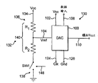
Referring now to accompanying drawing, more specifically,, an aspect, common simplified block diagram by the 130 digital analog converter systems that represent according to the theme invention have been described with reference to Fig. 1.Digital analog converter system 130 comprises: digital analog converter (DAC) 100 and mode controller 132.The DAC of DAC 100 expression any types.DAC 100 is typically integrated circuit (IC), but DAC 100 and nonessential be IC.In addition, although will be appreciated that mode controller 132 is shown as with DAC 100 separates, mode controller 132 can be whole with DAC 100.Therefore, DAC system 130 can be the whole of IC.
According to an aspect of theme invention, mode controller 132 is connected reference voltage input 104 and reference voltage (V
Cc) between.Mode controller 132 has to be shown as and is connected to reference voltage (V
Cc) reference voltage input 134.Mode controller 132 is with two states or mode operation.At a kind of state, mode controller 132 allow DAC 100 in first resolution up to corresponding to reference voltage (V
Cc) down work of maximum output voltage.At second kind of state, mode controller reduces maximum output voltage and (promptly is reduced to V in the resolution that increases DAC 100
CcPercentage).Mode controller 132 also is coupled with ground.
With reference to Fig. 2, described DAC system 130, and shown the various elements of mode controller 132 with the square frame form.Particularly, in a kind of form, mode controller 132 comprises: bleeder circuit/logical one 36 and switch/change-over circuit/logic (switch/switching circuitry/logic) 138.Bleeder circuit/logical one 36 is connected to reference voltage source (V via reference voltage input 134
Cc).Switch/change-over circuit/logical one 38 ground connection, and with two states or mode operation.First state or pattern are off conditions, and second state or pattern are the closed circuit conditions.
Bleeder circuit/logical one 36 is with 38 runnings of switch/change-over circuit/logical one, like this when switch/change-over circuit/logical one 38 at first state when (opening circuit), 36 runnings of bleeder circuit/logical one are to provide the maximum reference voltage (V of a hundred per cent (100%)
Cc) to reference voltage input 104, export 110 analog output voltage as aanalogvoltage in first resolution.Bleeder circuit/logical one 36 is also with 38 runnings of switch/change-over circuit/logical one, like this when switch/change-over circuit/logical one 38 when second state (closed circuit), bleeder circuit/logical one 36 turns round maximum reference voltage (V is provided to provide
Cc) percentage to reference voltage input 104, as the analog output voltage of the aanalogvoltage output 110 of second resolution bigger than first resolution.
Determine that by the circuit of bleeder circuit/logical one 36 offering DAC 100 by bleeder circuit/logical one 36 (offers Voltage Reference input V specifically
Ref104) maximum reference voltage (V
Cc) percentage.Calculate first resolution by following equation:
1/(2
N-1),
And calculate second resolution by following equation:
1/(2
N+1-1)。
From these two equatioies, double resolution as can be seen.In fact, the second resolution in fact twice than first resolution is big slightly, and this depends on the predetermined bit size of the input data bitstream of DAC 100.For example, if DAC 100 is 3 bit DAC, then first resolution is 1/7 (that is, having 7 grades from zero to maximum reference voltage), thereby second resolution is 1/15 (that is, having 15 grades from zero percentage to maximum reference voltage).As described below, the percentage that is provided as the reference voltage (maximum reference voltage) of maximum analog output voltage is determined by circuit component values.This can be called point of adjustment or transfer point.Although will present invention is described about a point of adjustment, can exist many point of adjustment maybe can have a continually varying point of adjustment.
Should be noted that second resolution that this DAC system provides it effectively to be increased.Same, term resolution effective, complete and/or part can be employed the increase with expression resolution.Theme DAC system so provides effective increase of resolution on the part of DAC, DAC structure or DAC system or the percentage range.Rephrase the statement, theme invention is similar to the resolution that half bit is provided on whole working range to DAC, DAC structure or DAC system, or the resolution of a bit is provided in percentage or part working range.
With reference to figure 3, shown that the exemplary circuit diagram of mode controller 132 is described.Specifically, bleeder circuit/logical one 36 is shown as voltage divider 140.In the exemplary embodiment, voltage divider 140 is made up of first resistor R 1 and second resistor R 2.First resistor R 1 is coupled to reference voltage V
CcReference voltage V
CCCan be for example ten (10) to lie prostrate.Second resistor R 2 is coupled to the change-over circuit 138 that comprises switch SW 1 herein.By the switch controlling signal that on thread switching control road 148, provides switch SW1 is controlled.Switch SW 1 is ground connection in turn.Switch controlling signal open and close switch SW 1.
R1/(R1+R2)。
The reference voltage that so offers DAC 100 depends on the value of resistor R 1 and R2.Therefore, when switch SW 1 closure, the maximum analog output voltage depends on the value of R1 and R2.
When R1=R2, the R1+R2 item can be changed into R1+R1, i.e. 2R1.Therefore, equation R1/ (R1+R2) can be rewritten as R1/2R1, but its abbreviation is 1/2.Therefore when R1=R2, the maximum reference voltage or the point of adjustment (with the maximum analog output voltage) that offer DAC 100 are that reference voltage is presented V
Cc1/2 or 50%.As generality, when R1<R2, point of adjustment is less than (<) 1/2V
CcOr 50%V
CcWhen R1>R2, point of adjustment is greater than (>) 1/2V
CcOr 50%V
Cc
With reference to Fig. 4, common optional embodiment by 150 digital analog converter (DAC) systems that represent has been described.In this embodiment, mode controller 132 being shown as may combine with DAC.But, will be appreciated that mode controller 132 can combine with DAC 100 or not combine with DAC 100.Except having first data, DAC 100 exports 1 aanalogvoltage output 110
1, second data export 2 aanalogvoltages output 110
2, and the 3rd data export 3 aanalogvoltages output 110
3Outside, DAC system 150 is to work with DAC system 130 identical modes as mentioned above.Each aanalogvoltage output 110
1, 110
2, 110
3For but digital input code provides separately the aanalogvoltage that equates output (OUT).In addition, 150 pairs of reference voltage working voltages of DAC system V
Cc, DAC 100 is used operating voltage.
Fig. 5 provides the chart 142 of the DAC system with 3 bit DAC, and it shows the function of output voltage as 3 digital bits input data.Output voltage range lies prostrate maximum V from minimum value of zero (0)
Max, wherein, along with digital input code changes to 111, V from 000
MaxCan be and the corresponding free voltage of the reference voltage that offers mode controller 132.When switch SW 1 is in off-state, V
MaxAlso corresponding with the reference voltage that offers DAC 100.In Figure 142, when switch closure and voltage divider 140 work, voltage V
Ref1Corresponding with the percentage of point of adjustment or maximum reference voltage.
In the example of in Figure 142, describing, the analog output voltage when line 144 representation switch SW1 are in open position.For digital input code 000, aanalogvoltage output is 0 volt.Along with digital input code advances to 111, analog output voltage increases to maximum V
Max(be reference voltage 100%).The resolution of line 144 is signable to be " X ".
Analog output voltage when line 146 representation switch SW1 are in the close position.For digital input code 000, aanalogvoltage output is 0 volt.Along with digital input code advances to 111, analog output voltage increases to maximum V
Ref1The percentage of the reference voltage of equation R1/ (R1+R2) (promptly according to).The resolution of line 144 is signable to be " 2X ".The slope of line 146 is less than the slope of line 144 as can be seen, and it shows in zero volt and maximum analog output voltage V
Ref1Between per step or the voltage increment of digital input code (resolution) less than lying prostrate the maximum analog output voltage V from zero
MaxBetween per step or the voltage increment of digital input code (resolution).
Therefore theme DAC system provides the resolution of the conversion of N-bit DAC.Specifically, theme DAC system allows when utilizing existing N-bit DAC or the DAC structure of N bit is provided, and realizes the resolution of N+1 bit on the percentage voltage range of DAC.For example use 3 bits, R2R ladder network DAC provides eight (8) comprising end points discrete trapezoidal point.If need 4 bit resolution DAC, then need the number of ten six (16) individual trapezoidal points.Use the present invention, for specific or given range, 3 bit DAC structures can be used for realizing the performance of 4 bits.
With reference to Fig. 6, the block diagram of exemplary electronic Adjustment System that is used for by TV signal receiver (TV signal) tuners of 200 expressions has been described, wherein can use aforesaid DAC system.But, should be understood that and the nonessential DAC described herein system that in electronics Adjustment System 200, uses.Electronics Adjustment System 200 running is with from RF TV signal source received RF (RF) TV signal (RF signal or input), and an intermediate frequency (IF) output is provided.Specifically, electronics Adjustment System 200 turns round with some frequency bands of the RF TV signal of reception such as VHF (in particular, 2 VHF frequency bands, frequency band 1 and frequency band 2) and UHF TV signal, and according to selected television channel, provides IF TV channel signal.
From receiving the RF signal by the RF signal source that RF input switch or separator provide such as cable TV, antenna etc.The RF signal that receives is input to U/V (UHF/VHF) separator 202, and this separator running is to isolate the UHF frequency band from the VHF frequency band.When selected channel was VHF frequency band TV signal, U/V separator 202 received control signal BSV (frequency band is selected VHF).Control signal BSV is produced by the PLL 222 that shows with PLL (phase-locked loop) IC form herein.Control signal BSV is the voltage that is produced in response to channel selecting signal by PLL 222.
The output of single tuned filter 208 is provided to RF amplifier (amp) 210.210 runnings of RF amplifier are to amplify the RF UHF signal from single tuned filter 208 according to RF AGC (automatic gain control) signal that is produced by TV signal receiver.RF amplifier 210 also turns round and selects signal (BSU) to receive by PLL 222 generations and from the UHF frequency band of PLL 222.The PLL response channel is selected signal and is produced UHF frequency band selection signal BSU.It is the ON/OFF signal of RF amplifier 210 that frequency band is selected signal BSU essence.
The output of RF amplifier 210 is offered double tunning (DT) filter 212.According to an aspect of theme invention, double-tuned filter 212 is worked on five (0-5) volt scope zero.Specifically, double-tuned filter 212 is being worked from the continuous analog voltage of zero to five (0-5) volt.From DAC 224 receive be marked as PRI zero to five vor signals.DAC 224 produces zero to five vor signals (that is continuous analog 0-5 vor signal) PRI in response to channel selecting signal.This PRI voltage signal allows the first of double-tuned filter 212 to carry out tuning to selected channel.Also receive and be marked as the zero of SEC to five vor signals from DAC 224.DAC 224 produces zero to five vor signals (that is continuous analog 0-5 vor signal) SEC in response to channel selecting signal.This SEC voltage signal allows the second portion of double-tuned filter 212 to carry out tuning to selected channel.
The output of double-tuned filter 212 is offered the blender/oscillator 214 that shows with the IC form.Will be appreciated that blender part can separate with oscillator section, but the combining of demonstration.Specifically, the output with double-tuned filter 212 offers blender 228.UHF local oscillator (LO) 226 has the output that is connected to blender 228.UHF LO 226 running to be receiving local oscillator (LO) tuning voltage signals from PLL 222, and produces tuning local oscillator signals.The PLL response channel is selected signal, produces LO tuning voltage signal.LO tuning voltage signal is from zero analog voltage signal to 30 (0-30) volt.UHF LO 226 also provides feedback with the form of LO drive signal to PLL 222.
228 pairs of tuning UHF local oscillator signals from UHF LO 226 of UHF blender combine with the output signal (selected channel) of double-tuned filter 212 or mix.The output of blender 228 is offered double tuned intermediate frequency (IF) filter 234.Double tunning IF filter 234 offers IF amplifier (amp) 236 with its output.Then, will output offers various numerals and the Simulation with I F parts (not shown) or the miscellaneous part of TV signal receiver as IF from the IF signal (selected television channel) of the amplification of IF amplifier 236.
In addition, single tuned filter 216 runnings are to receive by PLL 222 generations and therefore to select signal (BS 1/2) from the frequency band of PLL 222.Frequency band is selected in two VHF frequency bands of signal (BS 1/2) selection.Specifically, frequency band selection signal (BS 1/2) is the ON/OFF voltage signal that derives from channel selecting signal.
The output of single tuned filter 216 is provided to RF amplifier (amp) 218.218 runnings of RF amplifier are to amplify the RF VHF signal from single tuned filter 216 according to RF AGC (automatic gain control) signal that is produced by TV signal receiver.RF amplifier 218 also turns round to receive by PLL 222 generations and therefore to select signal (BSU) from the VHF frequency band of PLL 222.The PLL response channel is selected signal and is produced VHF frequency band selection signal BSV.It is the ON/OFF signal of RF amplifier 218 that frequency band is selected signal BSV essence.
The output of RF amplifier 218 is offered double tunning (DT) filter 220.According to an aspect of theme invention, double-tuned filter 220 is worked on five (0-5) volt scope zero.Specifically, double-tuned filter 220 is being worked from the continuous analog voltage of zero to five (0-5) volt.From DAC 224 receive be marked as PRI zero to five vor signals.DAC 224 produces zero to five vor signals (that is continuous analog 0-5 vor signal) PRI in response to channel selecting signal.This PRI voltage signal allows the first of double-tuned filter 220 to carry out tuning to selected channel.Also receive and be marked as the zero of SEC to five vor signals from DAC 224.DAC 224 produces zero to five vor signals (that is continuous analog 0-5 vor signal) SEC in response to channel selecting signal.This SEC voltage signal allows the second portion of double-tuned filter 220 to carry out tuning to selected channel.
In addition, double-tuned filter 220 runnings are to receive by PLL 222 generations and therefore to select signal (BS 1/2) from the frequency band of PLL 222.This frequency band is selected in two VHF frequency bands of signal (BS 1/2) selection.Specifically, frequency band selection signal (BS 1/2) is the ON/OFF voltage signal that derives from channel selecting signal.This frequency band is selected signal (BS 1/2) and is offered the identical of single tuned filter 216.
The output of double-tuned filter 220 is offered the blender/oscillator 214 that shows with the IC form.Will be appreciated that blender part can separate with oscillator section, but the combining of demonstration.Specifically, the output with double-tuned filter 220 offers blender 232.VHF local oscillator (LO) 230 has the output that is connected to blender 232.VHF LO 230 running to be receiving local oscillator (LO) tuning voltage signals from PLL 222, and produces tuning local oscillator signals.The PLL response channel is selected signal, produces LO tuning voltage signal.LO tuning voltage signal is from zero analog voltage signal to 30 (0-30) volt.VHF LO 230 also provides feedback with the form of LO drive signal to PLL 222.
232 pairs of tuning VHF local oscillator signals from VHF LO 230 of VHF blender combine with the output signal (selected channel) of double-tuned filter 220 or mix.The output of blender 232 is offered double tuned intermediate frequency (IF) filter 234.Double tunning IF filter 234 offers IF amplifier (amp) 236 with its output.Then, will output offers various numerals and the Simulation with I F parts (not shown) or the miscellaneous part of TV signal receiver as IF from the IF signal (selected television channel) of the amplification of IF amplifier 236.
Channel selecting signal is typical, but not necessarily, is produced by the input of the TV signal receiver response user with electronics Adjustment System 220.Channel selecting signal is offered DAC 224 and PLL222.Though considered the mode that other provide channel selecting signal, electronics Adjustment System 200 is shown as utilizes I
2C (or IIC) configuration/protocol.Same, I
2C clock line and I
2The C data wire is shown as and is connected to DAC 224 and PLL 222.To the continuous analog voltage signal of maximum voltage, described maximum voltage is five (5) volts with regard to DAC 224, is 30 (30) volts with regard to PLL 222 from zero (0) for PLL 222 and DAC 224 both generations.
In addition, be described to RF (radio frequency) part is used 5 volts of varactors, LO (local oscillator) part is used 30 volts of varactors, also can use other voltage varactors though should be noted that the electronics Adjustment System or the electronic tuning unit that will provide herein.According to the principle of theme invention, the voltage supply (with varactor) that is used for the RF part is different with the voltage supply (and varactor) that is used for the LO part.This difference preferably is illustrated in the voltage supply of RF part and voltage supply and the varactor that varactor (being the varactor voltage capacity) is lower than the LO part.Thereby, for example, RF part can use ten second of the three ten-day periods of the hot season power supply/varactor, and the LO part can be used 30 volts of power supply/varactors.In addition, power supply and/or varactor voltage can be or can not be each other function.
With reference to Fig. 7, the exemplary circuit diagram of the block diagram of the electronics Adjustment System that is used for Fig. 6 has been described.Will be appreciated that the circuit of Fig. 7 is worked in the mode of describing about Fig. 6.Therefore, only specifically describe some part of circuit 200.At first, by separator 202, RF input (IN) is separated with inductor L0 by capacitor C0 specifically.The UHF part is via capacitor C0 branch, and the VHF part is via inductor L0 branch.Resistor R0 provides increase of charge protection/eliminate and/or alleviates protection.Resistor R0 is coupled to inductor L0 and ground.
As noted above, UHF part 204 has the voltage-controlled single tuned filter 208 of varactor.Single tuned filter 208 comprises and low-voltage (being the 0-5 volt) varactor (variable capacitance diode) VR7 and capacitor C7 series reactor L8 and L9 in parallel.Series reactor L8 and L9 and varactor VR7 in parallel and capacitor C7 be ground connection.By resistor R 4 tuning voltage signal ST is provided to the node between varactor VR7 and the capacitor C7.Single tuned filter 208 changes electrical characteristics according to the voltage that is applied to varactor VR7.Like this, single tuned filter 208 can carry out tuning to specific UHF channel according to input voltage signal ST.
Single tuned filter 208 is via capacitor C9 and 210 couplings of RF amplifier.Amplifier 210 comprises two-door N NMOS N-channel MOS N (MOS) field-effect transistor (FET) T2.A door coupling of capacitor C9 and transistor T 2, and another door of transistor T 2 receives RF AGC signal.The source ground of transistor T 2.Inductor L10 and transistor drain coupling.Inductor L10 and PLL222 coupling are selected (BSU) signal to receive the UHF frequency band in due course.Apply or do not apply the BSU signal and cause amplifier work or do not work, amplifier work whether cause conduction with allow signal by or non-conducting not allow the signal process.RF amplifier 210 is via capacitor C10 and double-tuned filter 212 couplings.
Double-tuned filter 212 comprises the first order (stage) 250, and it is in the mutual conductance relation via each inductor L11 and L12 and the second level 252.The first order 250 comprises low-voltage (0-5 volt) varactor VR8, one end and capacitor C10 coupling, and the other end and capacitor C11 coupling, thus varactor VR8 connects with capacitor C11.Series connection varactor VR8 and capacitor C11 are in parallel with inductor 11.By resistor R 5 tuning voltage signal PR1 is provided to the node between varactor VR8 and the capacitor C11.The first order 250 changes electrical characteristics according to the voltage that is applied to varactor VR8.
Double-tuned filter 212 comprises the second level 252, and it is in the mutual conductance relation via each inductor L11 and L12 and the first order 250.The second level 252 comprises low-voltage (0-5 volt) varactor VR9, one end and inductor L12 coupling, and the other end and capacitor C12 coupling, thus varactor VR9 connects with capacitor C12, and varactor VR9 and capacitor C12 are in parallel with inductor L12.By resistor R 5 tuning voltage signal SEC is provided to the node between varactor VR9 and the capacitor C12.The second level changes electrical characteristics according to the voltage that is applied to varactor VR9.Like this, double-tuned filter 212 can carry out tuning to specific UHF channel according to input voltage signal PRI and SEC.By capacitor C13 the output of double-tuned filter 212 is provided to blender/oscillator IC 214.
As noted above, VHF part 206 has the voltage-controlled single tuned filter 216 of varactor.Single tuned filter 216 comprises inductor L1.Low-voltage (being the 0-5 volt) varactor (variable capacitance diode) VR1 one end and inductor L1 coupling, the other end and capacitor C1 coupling, thus VR1 connects with C1.Series connection varactor VR1 and capacitor C1 and inductor L2 that connects and L3 parallel connection.Capacitor C1 and inductor L3 be ground connection.By resistor R 1 tuning voltage signal ST is provided to the node between varactor VR1 and the capacitor C1.Single tuned filter 216 changes electrical characteristics according to the voltage that is applied to varactor VR1.Like this, single tuned filter 216 can carry out tuning to specific VHF channel according to input voltage signal ST.
Single tuned filter 216 is gone back response band and selected signal BS1, and is tuning with the frequency band that changes single tuned filter 216.Single tuned filter 216 also comprises low-voltage (0-5 volt) the varactor VR2 that connects with capacitor C2.Signal BS1 is applied between varactor VR2 and the capacitor C2.Series connection varactor VR2 and capacitor C2 placement in parallel with inductor L3.
Double-tuned filter 220 comprises the first order 254, its via two components other inductor L4 and L6, and L5 and L7 be in mutual conductance with the second level 256 and concern.The first order 254 comprises low-voltage (0-5 volt) varactor VR3, one end and amplifier 218 couplings, and the other end and capacitor C3 coupling, thus varactor VR3 connects with capacitor C3.Varactor VR3 and the capacitor C3 and inductor L4 that connects and L5 parallel connection of series connection.By resistor R 2 tuning voltage signal PRI is provided to the node between varactor VR3 and the capacitor C3.The first order 254 changes electrical characteristics according to the voltage that is applied to varactor VR3.
The first order 254 of double-tuned filter 220 is gone back response band and selected signal BS1, and is tuning with the frequency band of the first order 254 that changes double-tuned filter 220.The first order 254 also comprises low-voltage (0-5) the varactor VR4 that connects with capacitor C4.Signal BS1 is applied between varactor VR4 and the capacitor C4.Series connection varactor VR4 and capacitor C4 placement in parallel with inductor L5.
Double-tuned filter 220 comprises the second level 256, its via divide other inductor to L4 and L6, and L5 and L7 be in mutual conductance with the first order 254 and concern.The second level 256 comprises low-voltage (0-5 volt) varactor VR6, one end and inductor L6 coupling, and the other end and capacitor C6 coupling, thus varactor VR6 connects with capacitor C6, and varactor VR6 and capacitor C6 are in parallel with inductor L6 and L7.By resistor R 3 tuning voltage signal SEC is provided to the node between varactor VR6 and the capacitor C6.The second level 256 changes electrical characteristics according to the voltage that is applied to varactor VR6.
The second level 256 of double-tuned filter 220 is gone back response band and selected signal BS1, and is tuning with the frequency band of the second level 256 that changes double-tuned filter 220.The second level 256 also comprises low-voltage (0-5 volt) the varactor VR5 that connects with capacitor C5.Signal BS1 is applied between varactor VR5 and the capacitor C5.Series connection varactor VR5 and capacitor C5 placement in parallel with inductor L7.Like this, double-tuned filter 220 can select signal BS1 to carry out tuning to the specific VHF channel of special frequency band according to input voltage signal PRI and SEC and frequency band.By capacitor C7 the output of double-tuned filter 220 is provided to blender/oscillator IC 214.
Blender/oscillator 214 receives BSV or BSU control signal, to select to utilize which local oscillator.In addition, PLL 222 and 214 couplings of blender/oscillator, thus the tuning voltage that will derive from channel selecting signal provides to UHF local oscillator (LO) tuning part 238 and VHF local oscillator (LO) tuning part 240.238 runnings of UHF LO tuning part are to provide tuning according to channel selection.240 runnings of VHF LO tuning part are to provide tuning according to channel selection.
UHF LO tuning part 238 comprises high pressure (0-30 volt) the varactor VR10 that connects with capacitor C14.Series connection varactor VR10 and capacitor C14 placement in parallel with inductor L13.To provide to the node between varactor VR10 and the capacitor C14 from the 0-30 volt harmonic ringing of PLL 222 by resistor R 9.This provides tuning signal for blender/oscillator 214, and is tuning to carry out UHF.
VHF LO tuning part 240 comprises high pressure (0-30 volt) the varactor VR11 that connects with capacitor C15.Series connection varactor VR11 and capacitor C15 and inductor are to L14 and L15 placement in parallel.To provide to the node between varactor VR11 and the capacitor C15 from the 0-30 volt harmonic ringing of PLL 222 by resistor R 10.Inductor is that running selects the frequency band of signal BS1 to select signal circuit with response band to the tap between L14 and the L15.Select signal to provide on frequency band between varactor VR12 and the capacitor C16.This provides tuning signal for blender/oscillator 214, and is tuning to carry out VHF.
As mentioning herein, because the tuning characteristic of variable capacitance diode (varactor), above-mentioned DAC system is preferably in the exemplary electronic Adjustment System that is used for TV signal receiver (TV signal) tuner and uses.Specifically, the tuning characteristic of variable capacitance diode is that it has electric capacity (frequency) variation faster in the low voltage scope.As a result, this changes faster and has strengthened needed resolution (that is, higher resolution).But, in the high voltage scope, described variation slowly many, allow lower resolution.Although can use the DAC of high-resolution, the DAC of high-resolution is more expensive.In addition, more high-resolution DAC will waste resolution down at high voltage (with the frequency in the tuning frequency band).Therefore the DAC of the resolution of this conversion allows to use low resolution DAC and acquisition only to utilize the advantage of high-resolution in the scope of needs.
Although the present invention has been described as having decision design, can in disclosed spirit and scope, have made further modification to the present invention.Therefore the application attempts to utilize universal principle of the present invention to contain any adaptive variation of the present invention and use.In addition, the known or convention of described this area is to be contained in the present invention and within the qualification of accessory claim book.
Claims (19)
1. tuner is characterized in that:
The source of one RF signal;
One signal output point;
Be coupling in the source of described RF signal and the signal processing apparatus between the described signal output point, described signal processing apparatus comprises other first and second signal processing circuit of branch;
Described first and second signal processing circuits comprise other first and second tuned element of branch;
Be coupled to produce first controller of first control signal with described first tuned element;
Be coupled to produce second controller of second control signal with described second tuned element, described second control signal is independent of described first control signal; With
The deviation range of described first control signal is higher than the deviation signal of described second control signal.
2. tuner as claimed in claim 1 is characterized in that: described secondary signal treatment circuit comprises the first band signal treatment circuit and the second frequency band treatment circuit.
3. tuner as claimed in claim 1 is characterized in that: described first signal processing circuit comprises pierce circuit and described secondary signal treatment circuit comprises the RF tuning circuit.
4. tuner as claimed in claim 1 is characterized in that: described first controller comprises phase-locked loop and described second controller comprises digital analog converter.
5. tuner as claimed in claim 1, it is characterized in that: described first tuned element comprises first and second local oscillator circuits and described second tuned element that respond described first control signal and comprises first and second tunable optic filter elements that respond described second control signal.
6. tuner as claimed in claim 5, it is characterized in that: the described first tunable filter element comprises in response to the first single tuning tunable filter of the deviation range of described second control signal and the first double tunning tunable filter, with by selected frequency; Comprise the second single tuning tunable filter and the second double tunning tunable filter with the described second tunable filter element, with by selected frequency in response to the deviation range of described second control signal.
7. tuner as claimed in claim 6, it is characterized in that: each of the first and second single tuning tunable filters comprises the varactor of the described deviation range that responds described second control signal, comprise two varactors with each of the described first and second double tunning tunable filters, each varactor responds the described deviation range of described second control signal respectively.
8. tuner is characterized in that:
Be used to receive the unit of RF signal;
The unit that is used for output signal;
The unit that is used for processing RF signals, it is coupling between described unit that is used to receive the RF signal and the described unit that is used for output signal, and the described unit that is used for processing RF signals comprises a RF signal processing unit that is respectively applied for processing RF signals and the 2nd RF signal processing unit that is used for processing RF signals;
A described RF signal processing unit comprises the first module that is used for tuning RF signal;
Described the 2nd RF signal processing unit comprises the Unit second that is used for tuning RF signal;
Be used for tuning described first module first control unit coupling, that be used to produce first control signal;
Be used for tuning described Unit second second control unit coupling, that be used to produce second control signal, described second control signal is independent of described first control signal;
The deviation range of wherein said second control unit is higher than the deviation signal of described first control unit.
9. tuner as claimed in claim 8 is characterized in that, a described RF signal processing unit that is used for processing RF signals comprises: the unit that is used to handle the unit of first band signal and is used to handle second band signal.
10. tuner as claimed in claim 8 is characterized in that: the described Unit second that is used for processing RF signals comprises mixed cell.
11. tuner as claimed in claim 8 is characterized in that: described second control unit comprises phase-locked loop, and described first control unit comprises digital analog converter.
12. tuner as claimed in claim 8, it is characterized in that: describedly be used for tuning Unit second and comprise and be used to respond described second control signal producing Unit first and second of local oscillator signals, and describedly be used for tuning first module and comprise the Unit first and second that are used for the RF signal is carried out adjustable filtering.
13. tuner as claimed in claim 12, it is characterized in that: the described first single tuning tunable filter unit and the first double tunning tunable filter unit that is used for the described first module that the RF signal carries out adjustable filtering is comprised the described deviation range that responds described first control signal, with by selected frequency; And the described first single tuned filter unit and the second double tunning tunable filter unit that is used for described Unit second that the RF signal carries out adjustable filtering is comprised the described deviation range that responds described first control signal, with by selected frequency.
14. tuner as claimed in claim 13, it is characterized in that: each of the described first and second single tuning tunable filter unit comprises a varactor of the described deviation range that responds described first control signal, and each of the described first and second double tunning tunable filter unit comprises two varactors of the described deviation range that responds described first control signal respectively.
15. the tuning methods in TV signal receiver is characterized in that:
Receive a plurality of RF signals;
Produce first control signal with first deviation range by first controller;
According to the tuning a plurality of RF signals of described first control signal, to obtain one selected in the described RF signal;
Produce second control signal with second deviation range that is higher than first deviation range by second controller, described second control signal is independent of described first control signal;
Produce local oscillator signals according to second control signal; With
Described local oscillator signals is mixed with one that selectes described in the described RF signal, to produce the IF signal.
16. method as claim 15, it is characterized in that the step that is produced first control signal with first deviation range by first controller comprises step: produce first control signal by first controller that comprises digital analog converter with first deviation range.
17. the method as claim 15 is characterized in that, the step that is produced second control signal with second deviation range by second controller comprises step: produced second control signal with second deviation range by second controller that comprises phase-locked loop.
18. method as claim 15, it is characterized in that, according to described first control signal a plurality of RF signals are carried out tuning step and comprise step: according to described first control signal, via the double tunning tunable filter to and the first and second single tuning tunable filters in of selecting in the described RF signal.
19. method as claim 18, it is characterized in that, according to described first control signal, via the double tunning tunable filter to and the first and second single tuning tunable filters in one select one step in the described RF signal to comprise step: according to described first control signal, via two variable capacitance diodes of one variable capacitance diode in the first and second single tuning tunable filters and double tunning tunable filter to selecting in the described RF signal.
Applications Claiming Priority (2)
| Application Number | Priority Date | Filing Date | Title |
|---|---|---|---|
| US10/256,878 US6925291B2 (en) | 2002-09-27 | 2002-09-27 | Electronic alignment system for a television signal tuner |
| US10/256,878 | 2002-09-27 |
Publications (2)
| Publication Number | Publication Date |
|---|---|
| CN1497961A CN1497961A (en) | 2004-05-19 |
| CN100389604C true CN100389604C (en) | 2008-05-21 |
Family
ID=32029379
Family Applications (1)
| Application Number | Title | Priority Date | Filing Date |
|---|---|---|---|
| CNB031594786A Expired - Fee Related CN100389604C (en) | 2002-09-27 | 2003-09-27 | Electronic regulating system of TV. signal tuner |
Country Status (7)
| Country | Link |
|---|---|
| US (1) | US6925291B2 (en) |
| EP (1) | EP1411636B1 (en) |
| JP (2) | JP2004120759A (en) |
| KR (1) | KR101014613B1 (en) |
| CN (1) | CN100389604C (en) |
| MX (1) | MXPA03008707A (en) |
| MY (1) | MY136765A (en) |
Cited By (4)
| Publication number | Priority date | Publication date | Assignee | Title |
|---|---|---|---|---|
| KR101476482B1 (en) * | 2007-08-22 | 2014-12-24 | 이 아이 듀폰 디 네모아 앤드 캄파니 | Flame resistant spun staple yarns made from blends of fibers derived from diamino diphenyl sulfone, low thermal shrinkage fibers, flame resistant fibers, and antitstatic fibers and fabrics and garments made therefrom and methods for making same |
| KR101476483B1 (en) * | 2007-08-22 | 2014-12-24 | 이 아이 듀폰 디 네모아 앤드 캄파니 | Flame resistant spun staple yarns made from blends of fibers derived from diamino diphenyl sulfone and high modulus fibers and fabrics and garments made therefrom and methods for making same |
| KR101476875B1 (en) * | 2007-08-22 | 2014-12-26 | 이 아이 듀폰 디 네모아 앤드 캄파니 | Fibers comprising copolymers containing structures derived from 4.4' diamino diphenyl sulfone and a plurality of acid monomers and methods of making same |
| KR101476874B1 (en) * | 2007-08-22 | 2014-12-26 | 이 아이 듀폰 디 네모아 앤드 캄파니 | Flame resistant spun staple yarns made from blends of fibers derived from diamino diphenyl sulfone and modacrylic fibers and fabrics and garments made therefrom and methods for making same |
Families Citing this family (16)
| Publication number | Priority date | Publication date | Assignee | Title |
|---|---|---|---|---|
| US6925291B2 (en) * | 2002-09-27 | 2005-08-02 | Thomson Licensing S.A. | Electronic alignment system for a television signal tuner |
| US7884886B2 (en) * | 2003-10-27 | 2011-02-08 | Zoran Corporation | Integrated channel filter and method of operation |
| JP3106132U (en) * | 2004-06-23 | 2004-12-16 | アルプス電気株式会社 | Television tuner |
| US7304533B2 (en) * | 2005-04-15 | 2007-12-04 | Microtune (Texas), L.P. | Integrated channel filter using multiple resonant filters and method of operation |
| US7620382B2 (en) * | 2005-06-09 | 2009-11-17 | Alps Electric Co., Ltd. | Frequency converter capable of preventing level of intermediate frequency signal from lowering due to rise in temperature |
| KR100736043B1 (en) * | 2005-08-17 | 2007-07-06 | 삼성전자주식회사 | Tuner and Broadcast signal receiver including the same |
| EP2082482A2 (en) * | 2006-04-19 | 2009-07-29 | Nxp B.V. | Receiver comprising a radiofrequency splitter |
| KR101041504B1 (en) * | 2009-05-18 | 2011-06-16 | (주)티에이치엔 | Device for assembling and testing case of junction box |
| JP4816766B2 (en) * | 2009-06-03 | 2011-11-16 | カシオ計算機株式会社 | Radio wave receiver |
| RU2539880C2 (en) * | 2009-07-13 | 2015-01-27 | Сони Корпорейшн | Receiver |
| CN102859879B (en) * | 2010-05-13 | 2015-03-11 | 华为技术有限公司 | System and method for calibrating output frequency in phase locked loop |
| KR20120133587A (en) * | 2011-05-31 | 2012-12-11 | 삼성전기주식회사 | Terrestrial broadcasting receiver |
| JP2014171058A (en) * | 2013-03-01 | 2014-09-18 | Sony Corp | Receiver |
| US8928820B2 (en) * | 2013-03-13 | 2015-01-06 | Silcon Laboratories Inc. | Television tuner to capture a cable spectrum |
| US8885106B2 (en) | 2013-03-13 | 2014-11-11 | Silicon Laboratories Inc. | Multi-tuner using interpolative dividers |
| US11183974B2 (en) * | 2013-09-12 | 2021-11-23 | Dockon Ag | Logarithmic detector amplifier system in open-loop configuration for use as high sensitivity selective receiver without frequency conversion |
Citations (4)
| Publication number | Priority date | Publication date | Assignee | Title |
|---|---|---|---|---|
| US4481673A (en) * | 1983-03-28 | 1984-11-06 | Rca Corporation | RF Prom tracking for tuners |
| US4760535A (en) * | 1984-02-21 | 1988-07-26 | Telefunken Electronic Gmbh | Control circuit for tuning a high-frequency input circuit |
| US5678211A (en) * | 1992-08-28 | 1997-10-14 | Thomson Consumer Electronics, Inc. | Television tuning apparatus |
| WO2002027924A2 (en) * | 2000-09-25 | 2002-04-04 | Thomson Licensing S.A. | Apparatus and method for optimizing the level of rf signals based upon the information stored on a memory |
Family Cites Families (40)
| Publication number | Priority date | Publication date | Assignee | Title |
|---|---|---|---|---|
| JPS5567248A (en) * | 1978-11-15 | 1980-05-21 | Sanyo Electric Co Ltd | Frequency synthesizerrtype channel selection device |
| DE2902952C2 (en) * | 1979-01-26 | 1986-10-09 | ANT Nachrichtentechnik GmbH, 7150 Backnang | Direct mixing receiving system |
| JPS56141629A (en) * | 1980-04-08 | 1981-11-05 | Sony Corp | Synthesizer receiver |
| JPS5834631A (en) * | 1981-08-24 | 1983-03-01 | Sanyo Electric Co Ltd | Tuner |
| US4418427A (en) | 1982-03-30 | 1983-11-29 | Rca Corporation | Tuning system for a multi-band television receiver |
| US4476583A (en) | 1983-02-28 | 1984-10-09 | Rca Corporation | Electronic tracking for tuners |
| JPS607219A (en) * | 1983-06-27 | 1985-01-16 | Sony Corp | Electronic tuning receiver |
| JPS6166406A (en) * | 1984-09-10 | 1986-04-05 | Matsushita Electric Ind Co Ltd | Television tuner |
| JPS62179679A (en) * | 1986-02-03 | 1987-08-06 | Tokyo Keiki Co Ltd | Apparatus for controlling frequency of pulse radar |
| US4658437A (en) | 1985-03-01 | 1987-04-14 | Rca Corporation | Tuning voltage tracking arrangement |
| JPS61295722A (en) * | 1985-06-25 | 1986-12-26 | Mitsubishi Electric Corp | Gain control system of d/a converter |
| JPS6288415A (en) * | 1985-10-14 | 1987-04-22 | Sony Corp | Receiver |
| JPS62169527A (en) * | 1986-01-21 | 1987-07-25 | Mitsubishi Electric Corp | Digital-analog converter |
| JPS62141227U (en) * | 1986-02-26 | 1987-09-05 | ||
| JPH0432818Y2 (en) * | 1986-08-26 | 1992-08-06 | ||
| US4918532A (en) * | 1987-03-18 | 1990-04-17 | Connor Edward O | FM receiver method and system for weak microwave television signals |
| JPS63229907A (en) * | 1987-03-19 | 1988-09-26 | Sanyo Electric Co Ltd | Automatic tracking adjusting circuit |
| JPH0434576Y2 (en) * | 1987-03-30 | 1992-08-18 | ||
| JP2578951B2 (en) * | 1988-10-31 | 1997-02-05 | 日本電気株式会社 | Antenna tuning control circuit |
| US4996599A (en) | 1989-04-14 | 1991-02-26 | Rca Licensing Corporation | Television tuner oscillator with three point tracking |
| JPH03119829A (en) * | 1989-10-02 | 1991-05-22 | Hitachi Ltd | D/a converter |
| JPH03204205A (en) * | 1989-12-29 | 1991-09-05 | Nec Corp | Integrated circuit device |
| JP2529602Y2 (en) * | 1990-01-06 | 1997-03-19 | 関西日本電気株式会社 | High frequency equipment |
| JPH0470113A (en) * | 1990-07-11 | 1992-03-05 | Hitachi Ltd | Tuner circuit |
| JP2755842B2 (en) * | 1991-08-08 | 1998-05-25 | シャープ株式会社 | Superheterodyne receiver and its adjusting device |
| JPH0556640A (en) * | 1991-08-19 | 1993-03-05 | Sony Corp | Tuning-voltage generating circuit |
| US5428828A (en) | 1992-08-28 | 1995-06-27 | Thomson Consumer Electronics, Inc. | Television receiver tuning circuit |
| JPH06152423A (en) * | 1992-11-13 | 1994-05-31 | Nec Corp | D/a converter |
| JPH07231274A (en) * | 1994-02-21 | 1995-08-29 | Matsushita Electric Ind Co Ltd | Local oscillator circuit |
| US6035185A (en) | 1995-08-17 | 2000-03-07 | Zenith Electronics Corporation | Selective RF circuit with varactor tuned bandpass switched bandpass filters |
| CN1107378C (en) * | 1996-02-23 | 2003-04-30 | 松下通讯工业美国公司 | Method and system for determining integrity of received signal |
| JPH10209897A (en) * | 1997-01-20 | 1998-08-07 | Harada Ind Co Ltd | Variable tuning type antenna system |
| JP3388149B2 (en) * | 1997-07-25 | 2003-03-17 | 株式会社ケンウッド | Radio broadcast receiver |
| JP3612998B2 (en) * | 1998-04-08 | 2005-01-26 | 松下電器産業株式会社 | High frequency equipment |
| DE19904604A1 (en) | 1999-02-05 | 2000-06-15 | Temic Semiconductor Gmbh | Circuit layout and method for adjusting a band filter in a radio receiver has a band filter, a voltage-controlled oscillator, a tuner, a reference oscillator, a phase locked loop (PLL) actuator, an equalizer and a micro-controller. |
| KR100308299B1 (en) * | 1999-06-03 | 2001-10-29 | 구자홍 | Fine tuning adjustment method for digital television |
| JP2002124850A (en) * | 2000-10-17 | 2002-04-26 | Toko Inc | Electronic tuning circuit |
| US20020102957A1 (en) * | 2001-01-29 | 2002-08-01 | Han-Yang Tseng | Radio signal receiving control device and the control method for the same |
| JP2002261298A (en) * | 2001-03-02 | 2002-09-13 | Toko Inc | Variable-capacitance diode device |
| US6925291B2 (en) * | 2002-09-27 | 2005-08-02 | Thomson Licensing S.A. | Electronic alignment system for a television signal tuner |
-
2002
- 2002-09-27 US US10/256,878 patent/US6925291B2/en not_active Expired - Lifetime
-
2003
- 2003-09-25 JP JP2003332604A patent/JP2004120759A/en active Pending
- 2003-09-25 KR KR1020030066639A patent/KR101014613B1/en not_active IP Right Cessation
- 2003-09-25 MX MXPA03008707A patent/MXPA03008707A/en active IP Right Grant
- 2003-09-26 MY MYPI20033678A patent/MY136765A/en unknown
- 2003-09-27 CN CNB031594786A patent/CN100389604C/en not_active Expired - Fee Related
- 2003-09-29 EP EP03292389A patent/EP1411636B1/en not_active Expired - Fee Related
-
2010
- 2010-08-19 JP JP2010183938A patent/JP2010283876A/en active Pending
Patent Citations (4)
| Publication number | Priority date | Publication date | Assignee | Title |
|---|---|---|---|---|
| US4481673A (en) * | 1983-03-28 | 1984-11-06 | Rca Corporation | RF Prom tracking for tuners |
| US4760535A (en) * | 1984-02-21 | 1988-07-26 | Telefunken Electronic Gmbh | Control circuit for tuning a high-frequency input circuit |
| US5678211A (en) * | 1992-08-28 | 1997-10-14 | Thomson Consumer Electronics, Inc. | Television tuning apparatus |
| WO2002027924A2 (en) * | 2000-09-25 | 2002-04-04 | Thomson Licensing S.A. | Apparatus and method for optimizing the level of rf signals based upon the information stored on a memory |
Cited By (4)
| Publication number | Priority date | Publication date | Assignee | Title |
|---|---|---|---|---|
| KR101476482B1 (en) * | 2007-08-22 | 2014-12-24 | 이 아이 듀폰 디 네모아 앤드 캄파니 | Flame resistant spun staple yarns made from blends of fibers derived from diamino diphenyl sulfone, low thermal shrinkage fibers, flame resistant fibers, and antitstatic fibers and fabrics and garments made therefrom and methods for making same |
| KR101476483B1 (en) * | 2007-08-22 | 2014-12-24 | 이 아이 듀폰 디 네모아 앤드 캄파니 | Flame resistant spun staple yarns made from blends of fibers derived from diamino diphenyl sulfone and high modulus fibers and fabrics and garments made therefrom and methods for making same |
| KR101476875B1 (en) * | 2007-08-22 | 2014-12-26 | 이 아이 듀폰 디 네모아 앤드 캄파니 | Fibers comprising copolymers containing structures derived from 4.4' diamino diphenyl sulfone and a plurality of acid monomers and methods of making same |
| KR101476874B1 (en) * | 2007-08-22 | 2014-12-26 | 이 아이 듀폰 디 네모아 앤드 캄파니 | Flame resistant spun staple yarns made from blends of fibers derived from diamino diphenyl sulfone and modacrylic fibers and fabrics and garments made therefrom and methods for making same |
Also Published As
| Publication number | Publication date |
|---|---|
| MY136765A (en) | 2008-11-28 |
| US20040063410A1 (en) | 2004-04-01 |
| US6925291B2 (en) | 2005-08-02 |
| EP1411636A1 (en) | 2004-04-21 |
| CN1497961A (en) | 2004-05-19 |
| EP1411636B1 (en) | 2011-07-27 |
| KR20040027417A (en) | 2004-04-01 |
| JP2004120759A (en) | 2004-04-15 |
| MXPA03008707A (en) | 2004-09-10 |
| KR101014613B1 (en) | 2011-02-16 |
| JP2010283876A (en) | 2010-12-16 |
Similar Documents
| Publication | Publication Date | Title |
|---|---|---|
| CN100389604C (en) | Electronic regulating system of TV. signal tuner | |
| KR910001374B1 (en) | Television tuning system with electronic frequency adjustment apparatus | |
| US7102465B2 (en) | Frequency discrete LC filter bank | |
| US7095454B2 (en) | Broadband single conversion tuner integrated circuits | |
| US7403140B2 (en) | Receiver, digital-analog converter and tuning circuit | |
| US4271529A (en) | Tunable resonant circuits for a multi-band VHF/UHF/CATV tuner | |
| DE102016111432B4 (en) | Multi-stage digital-to-analog converter | |
| JP3264811B2 (en) | Voltage control variable tuning circuit | |
| EP1661243A2 (en) | Broadband integrated digitally tunable filters | |
| KR100304559B1 (en) | Selective rf circuit for double conversion tuner | |
| US6915121B2 (en) | Integrated tunable filter for broadband tuner | |
| JP3250785B2 (en) | TV tuner | |
| US20030207672A1 (en) | Wideband tuning circuit for low-voltage silicon process and method for generating a tuning frequency | |
| JPH0423842B2 (en) | ||
| US7015845B2 (en) | Digital to analog converter system | |
| KR100524509B1 (en) | Television tuner operating under low voltage | |
| MXPA97002782A (en) | Entry circuit for a televis tuner | |
| US7148726B2 (en) | Digital signal buffer circuit | |
| CN101553983A (en) | Active distributed signal splitting apparatus | |
| KR890004670B1 (en) | Convertable uhf generator | |
| KR900011294Y1 (en) | C.a.t.v. tuner | |
| JPH05152985A (en) | Channel selection system for radio receiver |
Legal Events
| Date | Code | Title | Description |
|---|---|---|---|
| C06 | Publication | ||
| PB01 | Publication | ||
| C10 | Entry into substantive examination | ||
| SE01 | Entry into force of request for substantive examination | ||
| C14 | Grant of patent or utility model | ||
| GR01 | Patent grant | ||
| CF01 | Termination of patent right due to non-payment of annual fee |
Granted publication date: 20080521 Termination date: 20170927 |
|
| CF01 | Termination of patent right due to non-payment of annual fee |