CN100367497C - Semiconductor device and method for fabricating the same - Google Patents
Semiconductor device and method for fabricating the same Download PDFInfo
- Publication number
- CN100367497C CN100367497C CNB031476562A CN03147656A CN100367497C CN 100367497 C CN100367497 C CN 100367497C CN B031476562 A CNB031476562 A CN B031476562A CN 03147656 A CN03147656 A CN 03147656A CN 100367497 C CN100367497 C CN 100367497C
- Authority
- CN
- China
- Prior art keywords
- wiring
- drain electrode
- interlayer dielectric
- grid
- semiconductor device
- Prior art date
- Legal status (The legal status is an assumption and is not a legal conclusion. Google has not performed a legal analysis and makes no representation as to the accuracy of the status listed.)
- Expired - Fee Related
Links
Images


Classifications
-
- H—ELECTRICITY
- H01—ELECTRIC ELEMENTS
- H01L—SEMICONDUCTOR DEVICES NOT COVERED BY CLASS H10
- H01L23/00—Details of semiconductor or other solid state devices
- H01L23/58—Structural electrical arrangements for semiconductor devices not otherwise provided for, e.g. in combination with batteries
- H01L23/62—Protection against overvoltage, e.g. fuses, shunts
-
- H—ELECTRICITY
- H01—ELECTRIC ELEMENTS
- H01L—SEMICONDUCTOR DEVICES NOT COVERED BY CLASS H10
- H01L27/00—Devices consisting of a plurality of semiconductor or other solid-state components formed in or on a common substrate
- H01L27/02—Devices consisting of a plurality of semiconductor or other solid-state components formed in or on a common substrate including semiconductor components specially adapted for rectifying, oscillating, amplifying or switching and having at least one potential-jump barrier or surface barrier; including integrated passive circuit elements with at least one potential-jump barrier or surface barrier
- H01L27/0203—Particular design considerations for integrated circuits
- H01L27/0248—Particular design considerations for integrated circuits for electrical or thermal protection, e.g. electrostatic discharge [ESD] protection
- H01L27/0251—Particular design considerations for integrated circuits for electrical or thermal protection, e.g. electrostatic discharge [ESD] protection for MOS devices
- H01L27/0266—Particular design considerations for integrated circuits for electrical or thermal protection, e.g. electrostatic discharge [ESD] protection for MOS devices using field effect transistors as protective elements
-
- H—ELECTRICITY
- H01—ELECTRIC ELEMENTS
- H01L—SEMICONDUCTOR DEVICES NOT COVERED BY CLASS H10
- H01L2924/00—Indexing scheme for arrangements or methods for connecting or disconnecting semiconductor or solid-state bodies as covered by H01L24/00
- H01L2924/0001—Technical content checked by a classifier
- H01L2924/0002—Not covered by any one of groups H01L24/00, H01L24/00 and H01L2224/00
Abstract
In a semiconductor device according to the present invention, an n-type MISFET 12 including a semiconductor substrate 11, a source region 16, a drain region 17 and a gate electrode 19 is provided. On the semiconductor substrate 11, a first interlevel insulating film 13 covering the MISFET 12, a second interlevel insulating film 14 and third interlevel insulating film 15 are provided. On the first interlevel insulating film 13, a first gate interconnect 25 for electrically connecting a gate electrode 19 and the outside, a first drain interconnect for electrically connecting the drain region and the outside are provided so as to face each other with part of a second interlevel insulating film 14 interposed therebetween.
Description
Technical field
The present invention relates to semiconductor device and manufacture method thereof, particularly relate to a kind of for protecting internal circuit to avoid semiconductor device and the manufacture method thereof that electrostatic breakdown uses.
Background technology
At the internal circuit of semiconductor device and the signal transmitting and receiving between the outside, carry out through input/output terminal subpad (pad).This input/output terminal subpad can not only be intended to drive the signal of internal circuit to the internal circuit feed, but also can the outside static that produces suddenly of feed.When the static value of internal circuit feed was big, the element that is arranged in the internal circuit will be destroyed.
In order to make internal circuit avoid electrostatic breakdown, in the inside of semiconductor device, between road and the input/output terminal subpad, electrostatic protection element is being set, or is having the electrostatic discharge protective circuit of electrostatic protection element.As electrostatic protection element commonly used, the parasitic bipolar transistor by source electrode (S)-substrate (B)-drain electrode (D) formation of MISFET is arranged.
Utilize Fig. 9 to tell about the structure of electrostatic protection element below.Fig. 9 is the schematic cross sectional view of the semiconductor device structure that utilizes NPN type parasitic bipolar transistor of expression prior art.
As shown in Figure 9, in the semiconductor device of prior art, internal circuit 81 is being set; Can between the outside of semiconductor device and internal circuit 81, carry out the input/output terminal subpad 82 of signal transmitting and receiving; Electrostatic protection element 83 that be connected, that have N type MISFET structure between internal circuit 81 and input/output terminal subpad 82.Electrostatic protection element 83 has: semiconductor substrate 90; The source area 91 of setting separated from each other in semiconductor substrate 90 and drain region 92; The source electrode 93 that on source area 91, is provided with; The drain electrode 94 that on drain region 92, is provided with; The gate insulating film 95 that on semiconductor substrate 90, is provided with; The gate electrode 96 that on gate insulating film 95, is provided with; The sidewall liner (side wall spacer) 97 that is provided with in the side of gate insulating film 95; And the resistance 98 that is connected with gate electrode 96.
The drain electrode 94 of electrostatic protection element 83 is connecting internal circuit 81 and input/output terminal subpad 82.In addition, source electrode 93, gate electrode 96 and semiconductor substrate 90 are connected with earthing potential 99, thereby all are grounded.Electrostatic protection element 81 is when playing a role as parasitic bipolar transistor, and drain region 92 becomes collector electrode 101, and source area 91 becomes emitter 100, and the zone in the semiconductor substrate 90 between source area 91 and drain region 92 then becomes base stage 102.Semiconductor substrate 90 was as the function of resistance, shown in ideograph when substrate resistance 104 played a role as parasitic bipolar transistor at electrostatic protection element 83.
Below, re-use Fig. 9 the operating principle of electrostatic protection element 83 is made a presentation.From the outside of semiconductor device, negative sense surplus (excess load) voltage that static is caused, when adding to input and output terminal pad 82 outward, electric current is by the direction diffluence of earthing potential 99 to input/output terminal subpad 82, thereby drains static.At this moment because electric current is followed the forward characteristic of the PN junction that is formed by the p type district that is connected with earthing potential 99 in the n type drain region in the semiconductor substrate 90 and the semiconductor substrate 90; so; the reverse superfluous voltage that adds to input and output terminal pad 82 outward is subjected to clamper, thereby internal circuit is carried out superfluous voltage protection.
On the other hand, when the superfluous voltage of forward was applied on the input/output terminal subpad 82, the pattern of electrostatic protection element 83 just switched to bipolar transistor by MISFET.Its concrete action is described in detail in detail below.When superfluous voltage was applied on the drain electrode 94 by input/output terminal subpad 82, electric current flowed to earthing potential 99 by drain electrode 94, semiconductor substrate 90 and source electrode 93, thus release electrostatic.Along with the rising of the applied voltage of drain electrode 94, that end in N type MISFET drain region 92, the collision ion increases all the more, thereby substrate current 103 is increased gradually, after substrate current 103 flows to substrate resistance 104, will produce voltage drop.Under the effect of this voltage drop, the current potential of base stage 102 will rise.After base potential rose to a certain degree, parasitic bipolar transistor will conducting, and big electric current just flows to emitter 100 (source area 91) by collector electrode 101 (drain region 92).Drain electrode applied voltage when this pattern by MISFET is switched to the pattern of bipolar transistor is called trigger voltage.
Figure 10 is the curve chart that the relation of the magnitude of voltage of characteristic and current value is returned in the expression sudden turn of events.Flow to the electric current of electrostatic protection element 83, follow the sudden turn of events shown in Figure 10 and return characteristic, so the voltage on the drain electrode 94 is limited in below the trigger voltage.Usually because of the puncture voltage of trigger voltage, so can make internal circuit not be subjected to the destruction of superfluous voltage less than internal circuit element.
In addition, resistance 98 shown in Figure 9 has the effect that reduces trigger voltage.Its principle is: the drain region 92 of MISFET, and end common and gate electrode 96 is overlapping, so, between gate-to-drain, just exist electric capacity.Under the state that forms this electric capacity, when the superfluous voltage of the forward of generation of static electricity imposed on the drain electrode 94, the charging and discharging currents that is produced by electric capacity will pass through gate electrode 96 and resistance 98, flows to earthing potential 99 from drain electrode 94 rapidly.Like this, on resistance 98, will produce voltage drop, thereby the current potential of gate electrode 96 is risen.After the current potential of gate electrode 96 rises, the electric current that flows between the drain electrode-source electrode is increased, thereby produce more collision ion.Like this, substrate current 103 increases, and the voltage drop that substrate resistance 104 causes increases thereupon, and therefore base potential rises, thereby makes the easy conducting of parasitic bipolar transistor.In sum, resistance 98 is set after, can at the superfluous voltage of the forward that is applied in generation of static electricity at that moment trigger voltage be descended.
[patent documentation 1]
Te Kaiping 3-73567 communique.
Yet, in the semiconductor device of prior art, exist following problems.
In general MISFET, in order to suppress to inject the deterioration of the gate insulating film that causes after the hot carrier, profile of impurities is designed to make the variation form slowly of the electric field of that end of drain electrode.Therefore, less by the substrate current that the collision ion causes, the voltage drop that substrate resistance is caused is also little, and trigger voltage is higher, causes parasitic bipolar transistor to be difficult for conducting.
Then, recent internal circuit has been thinned to below the 3nm with the grid electrode insulating film of MISFET, and the grid disintegration voltage also drops to below 10 volts.
So if under the trigger voltage condition with higher, when being applied in the superfluous voltage of forward that static causes, internal circuit will bear voltage more than the disintegration voltage with MISFET grid electrode insulating film, thereby the grid electrode insulating film is damaged.
Summary of the invention
, the objective of the invention is to for this reason, return the technology of the trigger voltage in the characteristic, a kind of semiconductor device and manufacture method thereof of high electrostatic protection ability is provided by adopting effective reduction sudden turn of events.
Semiconductor device of the present invention is characterized in that: comprising: semiconductor layer; The source area that in described semiconductor layer, is provided with; In described semiconductor layer with described source area from the drain region that is provided with; The grid electrode insulating film that on described semiconductor layer, is provided with; The gate electrode that on described grid electrode insulating film, is provided with; The 1st interlayer dielectric of the described gate electrode of covering that on described semiconductor layer, is provided with; On described the 1st interlayer dielectric, be provided with, and the 1st grid wiring that is electrically connected with described gate electrode; On described the 1st interlayer dielectric, be provided with, and the 1st drain electrode wiring that is electrically connected with described drain region; And on described the 1st interlayer dielectric, be provided with, and cover the 2nd interlayer dielectric of described the 1st grid wiring and described the 1st drain electrode wiring, part in a part in described the 1st drain electrode wiring and described the 1st grid wiring, across the part of described the 2nd interlayer dielectric, extend to ground relatively along the grid width direction.
Like this, owing between the 1st grid wiring and the 1st drain electrode wiring, can keep electric capacity,, make the easy conducting of parasitic bipolar transistor so can reduce trigger voltage.
In addition, semiconductor device of the present invention also is included in the 2nd drain electrode wiring that is electrically connected with described the 1st drain electrode wiring that is provided with on described the 2nd interlayer dielectric, thereby can in the 2nd drain electrode wiring the drain region is connected with the external electric of semiconductor device.
In addition, semiconductor device of the present invention, the thickness of described the 1st drain electrode wiring and described the 1st grid wiring is provided with to such an extent that be thicker than described the 2nd drain electrode wiring, thereby can keeps bigger electric capacity.
In addition, semiconductor device of the present invention in described the 2nd interlayer dielectric, by that a part of material that a part of clamping of the part in described the 1st drain electrode wiring and described the 1st grid wiring, is high dielectric, thereby can keeps bigger electric capacity.
In addition, semiconductor device of the present invention, described high dielectric, preferably silicon nitride.
In addition, semiconductor device of the present invention, also comprise: the 2nd grid wiring that is electrically connected with described the 1st grid wiring is set on described the 2nd interlayer dielectric, with the 3rd interlayer dielectric that on described the 2nd interlayer dielectric, is provided with and covers described the 2nd drain electrode wiring and the 2nd grid wiring, make a part in described the 2nd drain electrode wiring and the part in described the 2nd grid wiring, standing facing each other and extending, so just can keep bigger electric capacity.
In addition, semiconductor device of the present invention in described the 3rd interlayer dielectric, by that a part of material that a part of clamping of the part in described the 2nd drain electrode wiring and described the 2nd grid wiring, is high dielectric, thereby can keeps bigger electric capacity.
In addition, semiconductor device of the present invention, described high dielectric, preferably silicon nitride.
In addition, semiconductor device of the present invention, also comprise: the 1st source wiring be electrically connected with described source area is set on described the 1st interlayer dielectric, makes interval between described the 1st source wiring and described the 1st grid wiring greater than the interval between described the 1st drain electrode wiring and described the 1st grid wiring.Because the interval of the 1st drain electrode wiring and the 1st grid wiring is littler than the prior art, so can more effectively keep electric capacity between the 1st drain electrode wiring and the 1st grid wiring.
In addition, semiconductor device of the present invention, described drain region and internal circuit with the input and output terminal of signal conveys to described internal circuit can be connected, thereby impose on the input/output terminal period of the day from 11 p.m. to 1 a.m at the superfluous voltage that static causes, can prevent that also internal circuit is impaired.
In addition, semiconductor device of the present invention, described gate electrode preferably is connected with resistance.
The manufacture method of semiconductor device of the present invention is characterized in that: comprising: being situated between on semiconductor layer has gate insulating film ground to form the operation (a) of gate electrode; In described semiconductor layer, form the operation (b) of source area and drain region; After described operation (b), above described semiconductor layer, form the operation (c) of the 1st interlayer dielectric again; On described the 1st interlayer dielectric, form the operation (d) of the 1st grid wiring that is electrically connected with described gate electrode; On described the 1st interlayer dielectric, form the 1st drain electrode wiring be electrically connected with described drain region, and a part that makes the 1st drain electrode wiring on the grid width direction relative with the part of described the 1st grid wiring to operation (e); And the operation (f) that on described the 1st interlayer dielectric, forms the 2nd interlayer dielectric that covers described the 1st grid wiring and described the 1st drain electrode wiring.
Like this, utilize the electric capacity that keeps between the 1st grid wiring and the 1st drain electrode wiring, reduce trigger voltage, can produce the semiconductor device that parasitic bipolar transistor is easy to conducting.
In addition, the manufacture method of semiconductor device of the present invention, also comprise: on described the 2nd interlayer dielectric, form the operation (g) of the 2nd drain electrode wiring that is electrically connected with described the 1st drain electrode wiring, thereby can produce the semiconductor device that is connected with the external electric of semiconductor device by the 2nd drain electrode wiring.
In addition, the manufacture method of semiconductor device of the present invention makes the thickness of described the 1st drain electrode wiring and described the 1st grid wiring, greater than the thickness of described the 2nd drain electrode wiring, thereby can keep bigger electric capacity.
In addition, the manufacture method of semiconductor device of the present invention, also comprise: the 2nd grid wiring that on described the 2nd interlayer dielectric, forms and be electrically connected with described the 1st grid wiring, and a part that makes the 2nd grid wiring relative with the part of described the 2nd drain electrode wiring to operation (h), thereby can keep bigger electric capacity.
In addition, the manufacture method of semiconductor device of the present invention, also comprise: in described operation (h) afterwards, on described the 2nd interlayer dielectric, be formed up to a rare part and be the operation (j) of the 3rd interlayer dielectric that constitutes by high dielectric, thereby electric capacity is further increased.
In addition, the manufacture method of semiconductor device of the present invention in described operation (f), constitutes a part in described the 2nd interlayer dielectric with high dielectric, thereby electric capacity is further increased.
In addition, the manufacture method of semiconductor device of the present invention, also comprise: the operation (i) that on described the 1st interlayer dielectric, forms the 1st source wiring that is electrically connected with described source area, make interval between described the 1st source wiring and described the 1st grid wiring greater than the interval between described the 1st drain electrode wiring and described the 1st grid wiring, thereby can produce the 1st source wiring and the interval of the 1st grid wiring semiconductor device narrower than the interval of prior art.
Description of drawings
Fig. 1 is the profile of the layout of expression semiconductor device (a) in embodiment 1, (b)~(d) is the plane graph of expression wiring preparation.
Fig. 2 (a)~(e) is the profile of manufacturing process of the semiconductor device of expression embodiment 1.
Fig. 3 is the profile of structure of the semiconductor device of expression embodiment 2.
Fig. 4 (a)~(e) is the profile of manufacturing process of the semiconductor device of expression embodiment 2.
Fig. 5 is in embodiment 3, and (a) and (b) are plane graphs of expression wiring preparation, (c)~(d) is that expression reaches (B)-(B) section of structure of hatching line along (A)-(A) hatching line.
Fig. 6 (a)~(e) is the profile along (B)-(B) hatching line of manufacturing process of the semiconductor device of expression embodiment 3.
Fig. 7 (a) and (b) are to be illustrated in the semiconductor device of embodiment 4, reach (B)-(B) section of structure of hatching line along (A)-(A) hatching line.
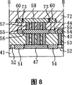
Fig. 8 is the profile of the architecture advances example of expression embodiment 4.
Fig. 9 is the profile of tactic pattern of semiconductor device of the parasitic bipolar transistor that utilizes the NPN type of expression prior art.
Figure 10 is the curve chart that the relation of the magnitude of voltage of characteristic and current value is returned in the expression sudden turn of events.
Among the figure:
11 semiconductor substrates
12N type MISFET
13 the 1st interlayer dielectrics
14 the 2nd interlayer dielectrics
15 the 3rd interlayer dielectrics
16 source areas
17 drain regions
18 gate insulating films
19 gate electrodes
20 sidewalls
21 element separation
22 protection distances (guard band)
23 the 1st contacts (contact plug)
24 the 1st source wiring
25 the 1st grid wirings
26 the 1st drain electrode wirings
27 the 2nd contacts
28 the 2nd drain electrode wirings
29 electric capacity maintaining parts
30 the 1st grid wirings
31 the 1st drain electrode wirings
32 the 1st source wiring
33 electric capacity maintaining parts
41 semiconductor substrates
42N type MISFET
43 the 1st interlayer dielectrics
44 the 2nd interlayer dielectrics
45 source areas
46 drain regions
49 gate electrodes
52 protection distances
53 the 1st contacts
54 the 1st source wiring
55 the 1st grid wirings
56 the 1st drain electrode wirings
57 the 2nd contacts
58 the 2nd drain electrode wirings
60 the 2nd grid wirings
71 high dielectric dielectric films
72 dielectric films
73 high dielectrics
Embodiment
(embodiment 1)
Below in embodiment 1, be accumulated in electric capacity between the 1st grid wiring and the 1st drain electrode wiring by increase, thereby semiconductor device and manufacture method thereof that trigger voltage is descended are done an explanation.
At first, utilize Fig. 1 (a)~(d), the semiconductor device in the present embodiment is done an explanation.Fig. 1 (a) is the profile of the semiconductor device layout among the expression embodiment 1, Fig. 1 (b) is the plane graph of the top layout of expression semiconductor substrate, Fig. 1 (c) is the plane graph that expression is arranged on the wiring preparation on the 1st interlayer dielectric, and Fig. 1 (a) then is the plane graph that expression is arranged on the wiring preparation on the 2nd interlayer dielectric.In addition, the section shown in Fig. 1 (a) is the section of (A)-(A) hatching line among Fig. 1 (b)~(d).In addition, in Fig. 1 (a)~(d), input/output terminal subpad and internal circuit are not shown.
Shown in Fig. 1 (a), in the semiconductor device of present embodiment, in the semiconductor substrate (semiconductor layer) 11; as electrostatic protection element; N type MISFET12 is being set, on semiconductor substrate 11, stacked the 1st interlayer dielectric the 13, the 2nd interlayer dielectric 14 and the 3rd interlayer dielectric 15.
N type MISFET12 is arranged among the component forming region Rr of semiconductor substrate 11.N type MISFET12 comprises: containing concentration is 3.5 * 10
17Cm
-3The semiconductor substrate 11 of impurity; The concentration that contains that is separated from each other setting in semiconductor substrate 11 is 4.0 * 10
20Cm
-3The source electrode 16 and the drain region 17 of N type impurity; The thickness that is provided with on the zone that by source area 16 and drain region 17 clampings in semiconductor substrate 11 is the dielectric film 18 of 7.5nm; The grid length that is provided with on gate insulating film 18 is the gate electrode 19 of 40nm; And the sidewall liner 20 that constitutes by insulant that is provided with in the side of gate electrode 19.The gate electrode 19 of N type MISFET12 and source area 16 by the 1st contact 23 and the 1st grid wiring 25 and the 1st source wiring 24 that are arranged on the 1st interlayer dielectric 13, are connected with external electric.17 of the drain regions of N type MISFET12 pass through the 1st contact the 23, the 1st drain electrode wiring the 26, the 2nd contact 27 and the 2nd drain electrode wiring 28 is connected with external electric.
Shown in Fig. 1 (b), the side of component forming region Rr, the element separation 21 that is made of insulating barrier surrounds.The side of element separation 21, then being contained concentration is 2 * 10
20Cm
-3The protection distance 22 of p type impurity surround.Source area 16 in component forming region Rr, drain region 17, gate electrode 19 and above the protection distance 22 are being provided with the 1st contact 23 that runs through the 1st interlayer dielectric 13 (seeing Fig. 1 (a)).
In Fig. 1 (c), not shown the 1st interlayer dielectric 13.The parts that are arranged on the top of the 1st interlayer dielectric 13 represent with solid line that all the parts that are arranged on the below of the 1st interlayer dielectric 13 then dot.In addition, the thickness of the 1st interlayer dielectric 13 is configured to 480nm.Shown in Fig. 1 (c), gate electrode 19 (seeing Fig. 1 (b)) and thickness are that the 1st grid wiring 25 of 250nm is electrically connected then.The 1st grid wiring 25 is connected with the earthing potential (not shown) by the resistance (not shown).Source area 16 (seeing Fig. 1 (b)) and thickness are that the 1st source wiring 24 of 250nm is electrically connected.After the 1st source wiring 24 extends to the top that is arranged on the 1st contact 23 on the protection distance 22, be connected with the earthing potential (not shown).Drain region 17 (seeing Fig. 1 (b)) and thickness are that the 1st drain electrode wiring 26 of 250nm is electrically connected.On the 1st drain electrode wiring 26, the 2nd contact 27 is being set.
In the semiconductor device of present embodiment, shown in Fig. 1 (c), the 1st grid wiring 25 above gate electrode 19, with the parallel sided of the 1st drain electrode wiring 26 and to be extended.In other words, the 1st grid wiring 25 not only is being provided with in the zone of earthing potential above the 1st contact 23, but also along or be provided with round the side of the 1st drain electrode wiring 26.In addition, the zone with the part of the part of the 1st grid wiring 25 and the 1st drain electrode wiring 26 extends in parallel is called electric capacity maintaining part 29.The capacitance of electric capacity maintaining part 29 depends on the face-off area and the interval of the 1st grid wiring 25 and the 1st drain electrode wiring 26.In other words, increase the face-off area of the 1st grid wiring 25 and the 1st drain electrode wiring 26, perhaps dwindle the interval of the 1st grid wiring 25 and the 1st drain electrode wiring 26, just can increase capacitance.
In the past, grid wiring only was connected with gate contacts usually, and did not extend to the top of gate electrode.From the arrangement angles of wiring, when grid wiring is extended to the top of gate electrode, the same from the interval (distance) of grid wiring to the 1 drain electrode wiring and the 1st source wiring.Different therewith, in the present embodiment, grid wiring has extended to the top of gate electrode 19, and from the interval of the 1st grid wiring 25 to the 1st drain electrode wirings 26 less than interval from the 1st grid wiring 25 to the 1st source wiring 24.Especially with the interval of the 1st grid wiring 25 to the 1st drain electrode wirings 26, during little minimum value (about 0.2 μ m) to the wiring configuration, just can keep bigger capacitance.
In addition, owing to dwindled the interval of the 1st grid wiring 25 and the 1st drain electrode wiring 26, so, both can increase the width of the 1st grid wiring 25, also can increase the width of the 1st drain electrode wiring 26.
In Fig. 1 (d), not shown the 2nd interlayer dielectric 14.The parts that are arranged on the top of the 2nd interlayer dielectric 14 represent with solid line that all the parts that are arranged on the below of the 2nd interlayer dielectric 14 then dot.In addition, the thickness of the 2nd interlayer dielectric 14 is configured to 700nm.The 1st drain electrode wiring 26 (seeing Fig. 1 (c)) and thickness are that the 2nd source wiring 28 of 340nm is electrically connected.28 of the 2nd drain electrode wirings are connected with the internal circuit (not shown) with input/output terminal subpad (not shown).
Below, utilize Fig. 2 (a)~(e) that the manufacturing method for semiconductor device of present embodiment is made a presentation.Fig. 2 (a)~(e) is the profile of manufacturing process of the semiconductor device of expression embodiment 1.
At first, in the operation shown in Fig. 2 (a), adopt the manufacturing process of common N type MISFET, the protection distance 22 that on semiconductor substrate 11, forms element separation 21 and constitute by p type diffused layer.In the component forming region Rr of semiconductor substrate 11, form the N type MISFET12 that constitutes by source area 16, drain region 17, gate insulating film 18, gate electrode 19, sidewall liner 20.
Then, in the operation shown in Fig. 2 (b),, on N type MISFET12, pile up the 1st interlayer dielectric 13 that constitutes by BPSG (Boron-Phospho Silicate Glass) film by methods such as CVD, handle by CMP, make the surface of the 1st interlayer dielectric 13 be tending towards smooth.By photoetch method technology and dry corrosion technology, form the contact hole that runs through the 1st interlayer dielectric 13 again.Then tungsten (W) is inserted contact hole, handle, make it to have an even surface, thereby form the 1st contact 23 by CMP.The 1st contact 23 is configured to arrive source area 16, drain region 17, the state of gate electrode 19 and protection distance 22.
In the operation shown in Fig. 2 (c),, pile up the electrically conductive film that constitutes by wiring materials such as lead again by the method for sputter.On electrically conductive film, make wiring diagram by photoetch method technology and dry corrosion technology again, thereby form the 1st grid wiring the 25, the 1st source wiring 24 and the 1st drain electrode wiring 26 of the configuration mode shown in Fig. 1 (c).At this moment, the part of the part of the 1st grid wiring 25 and the 1st drain electrode wiring 26 becomes electric capacity maintaining part 29.
Then, in the operation shown in Fig. 2 (d),, on the 1st interlayer dielectric 13, pile up FSG (Fluorinated Silicate Glass) film by methods such as CVD, by the CMP method make it to be tending towards smooth after, just form the 2nd interlayer dielectric 14.Then, again by photoetch method technology and dry corrosion technology, form the contact hole that runs through the 2nd interlayer dielectric 14.Then tungsten (W) is inserted contact hole, handles by CMP, make it to be tending towards smooth after, just form the 2nd contact 27.
At last, in the operation shown in Fig. 2 (e), pile up the electrically conductive film that constitutes by wirings such as aluminium by sputter.By photoetch method technology and dry corrosion technology, on electrically conductive film, make wiring diagram again, thereby form the 2nd drain electrode wiring 28 of the sort of configuration mode shown in Fig. 1 (d).Then, by methods such as CVD, on the 2nd layer of dielectric film 14, form the 3rd layer of dielectric film 15 (seeing Fig. 1 (a)) that constitutes by FSG.By above operation, just produce the semiconductor device of present embodiment.
In the present embodiment, the 1st grid wiring 25 has extended to the top of the 1st gate electrode 19, and the 1st grid wiring 25 and 26 of the 1st drain electrode wirings maintain narrow spacing parallel arranging and form.Like this, the electric capacity between the grid-leakage just semiconductor device than prior art is big, so can reduce trigger voltage.Below, its reason is set forth.
The drain region 17 of N type MISFET12 is overlapping with the end of gate electrode 19, so exist electric capacity between grid-leakage.Under the state that has formed electric capacity, when the forward surplus voltage by generation of static electricity, when being applied on the drain region 17, the charging and discharging currents that electric capacity produces will flow to the earthing potential (not shown) rapidly by gate electrode 19.At this moment, thus charging and discharging currents flows to the current potential that makes gate electrode 19 in the resistance shown in Figure 9 98 to rise.In the semiconductor device of present embodiment, because the capacity ratio between grid-leakage was big in the past, so the current potential rising De Genggao of gate electrode 19, the electric current that flows through between grid-leakage is also bigger, thereby has quickened the activity of collision ion.Like this, because substrate current 103 shown in Figure 9 increases, so the current potential of base current 102 rises easily, trigger voltage descends, and makes the easy conducting of parasitic bipolar transistor.
In sum, in the present invention, by the electric capacity between the grid-leakage that strengthens N type MISFET12, it is lower than the prior art to make the sudden turn of events return the trigger voltage of characteristic, thus can prevent that bigger static from imposing on internal circuit the time to its infringement that causes.
(embodiment 2)
Fig. 3 is the profile of structure of the semiconductor device of expression embodiment 2.In the semiconductor device of present embodiment, with the difference of embodiment 1 be the 1st grid wiring 30 and the 1st drain electrode wiring 31, its Film Thickness Ratio prior art thick.Like this, the thickness of the 1st grid wiring 30 and the 1st drain electrode wiring 31, also thick than the 2nd drain electrode wiring 28.And in the semiconductor device of prior art, be connected with external electric in order to make minute sized element (MISFET), it is thick to be provided with than the 1st drain electrode wiring the thickness of the 2nd drain electrode wiring.In addition, the thickness of the 1st grid wiring 30 of present embodiment and the 1st drain electrode wiring 31 is the best with 500nm~700nm.At this moment, neither can influence other layer, can keep bigger electric capacity again.
The plane figure of present embodiment, so the same with shown in Fig. 1 (b)~(d) among the embodiment 1 is diagram and introduce and all omitted.
Below, utilize Fig. 4 (a)~(e) that the manufacture method of the semiconductor device of present embodiment is made a presentation.Fig. 4 (a)~(e) is the profile of manufacturing process of the semiconductor device of expression embodiment 2.Because the semiconductor device plane preparing mode of present embodiment is the same with embodiment 1, so also will consult Fig. 1 (b)~(d).
At first, in the operation shown in Fig. 4 (a), adopt the manufacturing process of common MISFET, the protection distance 22 that on semiconductor substrate 11, forms element separation 21 and constitute by p type diffused layer.Forming the N type MISFET12 that formation is made of source area 16, drain region 17, gate insulating film 18 and gate electrode 19, side wall surface liner 20 on the region R r on the element of semiconductor substrate 11.
Then, in the operation shown in Fig. 4 (b),, pile up the 1st interlayer dielectric 13 that constitutes by BPSG at N type MISFET12 by methods such as CVD.Handle by CMP again, make the 1st interlayer dielectric 13 surfaces be tending towards smooth,, form the contact hole that runs through the 1st interlayer dielectric 13 again by photoetch method technology and dry corrosion technology.Then, (W) inserts in the contact hole with tungsten, adopts CMP to handle and makes it to have an even surface, thereby form the 1st contact 23.As the 1st contact 23, be arranged to arrive source area 16, drain region 17, gate electrode 19 and protection distance 22.
Follow, in the operation shown in Fig. 4 (c), piling up the thickness that is made of wiring materials such as aluminium by the method for sputter is the electrically conductive film of 500nm again.Adopt photoetch method technology and dry corrosion technology again, on electrically conductive film, make wiring diagram, thereby produce the 1st grid wiring the 30, the 1st source wiring 32 and the 1st drain electrode wiring 31 of the sort of planar configuration pattern shown in Fig. 1 (c).At this moment, the part of the part of the 1st grid wiring 30 and the 1st drain electrode wiring 31 becomes electric capacity maintaining part 33.In electric capacity maintaining part 33, the area that the side of the 1st grid wiring 30 and the 1st drain electrode wiring 31 stands facing each other mutually is bigger than embodiment's 1.
In addition, in the operation shown in Fig. 4 (d), the 1st grid wiring the 30, the 1st source wiring 32 and the 1st drain electrode wiring 31 are mapped on same electrically conductive film and are formed.So the 1st source wiring 32 also can be thicker than originally.
In the operation shown in Fig. 4 (d), methods such as employing CVD are piled up fsg film on the 1st interlayer dielectric 13, and make it to be tending towards smooth by the CMP method, form the 2nd interlayer dielectric 14.Then, form the contact hole that runs through the 2nd interlayer dielectric 14 by photoetch method technology and dry corrosion technology.Then, (W) inserts in the contact hole with tungsten, and makes it smooth by the CMP method, thereby forms the 2nd contact 27.
At last, in the operation shown in Fig. 4 (e), piling up the thickness that is made of wiring materials such as aluminium by the method for sputter is the electrically conductive film of 340nm.Adopt photoetch method technology and dry corrosion technology again, on electrically conductive film, make wiring diagram, thereby form the 2nd drain electrode wiring 28 with the sort of plane figure pattern shown in Fig. 1 (d).Then, adopt method such as CVD on the 2nd interlayer dielectric 14, to form the 3rd interlayer dielectric 15 (seeing Fig. 3 (a)) that constitutes by FSG.By above operation, just can produce the semiconductor device of present embodiment.
In the present embodiment, can obtain the effect identical with embodiment 1.Further will serve as the thickness of the electrically conductive film of the 1st drain electrode wiring 31 in the present embodiment, do to such an extent that serve as the thickness (being about 250nm) of the electrically conductive film of the 2nd drain electrode wiring 31 in the semiconductor device greater than prior art and serve as the thickness (being about 340nm) of the electrically conductive film of the 2nd drain electrode wiring 31.Just can make electric capacity between grid-leakage greater than embodiment 1, thereby can reduce the trigger voltage that characteristic is returned in the sudden turn of events more effectively.
(embodiment 3)
Embodiment 3 is in the wiring of embodiment 1, adds the wiring of embodiment 2, thereby keeps the electric capacity between grid-leakage.Below this embodiment is made a presentation.
At first, utilize Fig. 5 (a)~(d) that the semiconductor device of present embodiment is made a presentation.The semiconductor device of present embodiment is being provided with the 1st interlayer dielectric the 43, the 2nd interlayer dielectric 44 and the 3rd interlayer dielectric 45 on the semiconductor substrate 41 with N type MISFET42.In this semiconductor device, Fig. 5 (a) is the plane graph that expression is arranged on the wiring preparation on the 1st interlayer dielectric, Fig. 5 (b) is the plane graph that expression is arranged on the wiring preparation on the 2nd interlayer dielectric, Fig. 5 (c) is the profile of expression along the structure of (A)-(A) hatching line of semiconductor device, and Fig. 5 (d) is along the profile of the structure of (B)-(B) hatching line that intersects vertically with (A)-(A) hatching line in the expression semiconductor device.In addition, at Fig. 5 (a)~(d) input/output terminal subpad and internal circuit are not shown.
Embodiment 3 with the difference of embodiment 1 is: the 1st grid wiring 55 is connected with the 2nd grid wiring 60 by the 2nd contact 57, and the 2nd grid wiring 60 is parallel and approaching with the 2nd drain electrode wiring 58.Below, narrate its concrete structure, but the structure identical with embodiment 1 told about no longer then.
Shown in Fig. 5 (a), (see Fig. 5 (c)) forming thickness on the 1st interlayer dielectric 43 is the 1st source wiring the 54, the 1st grid wiring 55 and the 1st drain electrode wiring 56 of 250nm.The 1st source wiring 54 extends to the top that is arranged on the 1st contact 53 on the protection distance 52 from the top of source area 46 (seeing Fig. 5 (c)), is connected with the earthing potential (not shown).The 1st grid wiring 55 is arranged on the top of gate electrode 49 (seeing Fig. 5 (c)), is connected with the earthing potential (not shown) by the resistance (not shown).The 1st drain electrode wiring 56 is arranged on the top of source area 47 (seeing Fig. 5 (c)), and its side is surrounded by the 1st grid wiring 55.
Shown in Fig. 5 (b), on the 2nd interlayer dielectric 44, the 2nd drain electrode wiring 58 and the 2nd grid wiring 60 are being set.The former cladding element forms district Rr and extends to the length direction of grid; The latter then extends along the side surface direction of the 2nd drain electrode wiring.
The gate electrode 49 that is provided with on semiconductor substrate 41 shown in Fig. 5 (c), is connected with the 1st grid wiring 55 by the 1st contact 53.55 of the 1st grid wirings are connected with the 2nd grid wiring 60 by the 2nd contact 57 shown in Fig. 5 (d).
The source area 46 that is provided with in semiconductor substrate 41 then shown in Fig. 5 (c), is connected with the 1st source wiring 54 by the 1st contact 53.
The drain region 47 that is provided with in semiconductor substrate 41 then shown in Fig. 5 (c), by the 1st contact the 53, the 1st drain electrode wiring 56 and the 2nd contact 57, is connected with the 2nd drain electrode wiring 58.
Below, utilize Fig. 6 (a)~(e) that the manufacture method of the semiconductor device of present embodiment is illustrated.Fig. 6 (a)~(e) is the profile along (B)-(B) hatching line of manufacturing process of the semiconductor device of expression embodiment 3.
At first, in the operation shown in Fig. 6 (a), adopt the manufacturing process of common N type MISFET, the protection distance 52 that on semiconductor substrate 41, forms element separation 51 and constitute by p type diffused layer.Forming the N type MISFET12 (seeing Fig. 5 (c)) that comprises drain region 47 on the formation region R r on the element of semiconductor substrate 41.
Then, in the operation shown in Fig. 6 (b), adopt methods such as CVD, on semiconductor substrate 41, pile up the 1st interlayer dielectric 43 that constitutes by bpsg film, handle by CMP again, make the 1st interlayer dielectric 43 surfaces be tending towards smooth.By photoetch method technology and dry corrosion technology, form the contact hole that runs through the 1st interlayer dielectric 43 again.Then, (W) inserts in the contact hole with tungsten, adopts CMP to handle and makes it to have an even surface, thereby form the 1st contact 53.The 1st contact 53 is configured to arrive the source area 46 shown in Fig. 5 (c), drain region 47, gate electrode 49 and protection distance 52.
Follow again, in the operation shown in Fig. 6 (c), pile up the electrically conductive film that constitutes by wiring materials such as aluminium by the method for sputter.Adopt photoetch method technology and dry corrosion technology again, on electrically conductive film, make wiring diagram, thereby produce the 1st grid wiring the 55, the 1st source wiring 54 and the 1st drain electrode wiring 56 of the sort of planar configuration pattern shown in Fig. 5 (a).
Then in the operation shown in Fig. 6 (d), methods such as employing CVD are piled up fsg film on the 1st interlayer dielectric 43, and make it to be tending towards smooth by the CMP method, form the 2nd interlayer dielectric 44.Then, form the contact hole that runs through the 2nd interlayer dielectric 44 by photoetch method technology and dry corrosion technology.Then, tungsten is inserted in the contact hole, and made it smooth, thereby form the 2nd contact 57 by the CMP method.The 2nd contact 57 is arranged to arrive the 1st grid wiring 55 and the 1st drain electrode wiring 56.
At last, in the operation shown in Fig. 6 (e), pile up the electrically conductive film that constitutes by wiring materials such as aluminium by the method for sputter.Adopt photoetch method technology and dry corrosion technology again, on electrically conductive film, make wiring diagram, thereby form the 2nd grid wiring 60 and the 2nd drain electrode wiring 58 with the sort of plane figure pattern shown in Fig. 5 (b).By above operation, just can produce the semiconductor device of present embodiment.
In the present embodiment, can not only between the 1st grid wiring 55 and the 1st drain electrode wiring 56, keep electric capacity, and can also between the 2nd grid wiring 60 and the 2nd drain electrode wiring 58, keep electric capacity.So can effectively reduce the trigger voltage that characteristic is returned in the sudden turn of events more.Like this, just can prevent that big static is applied to the problem that produces on the internal circuit.
(embodiment 4)
Among the embodiment 4 embodiment 3 some improvement have been done.Below this is made a presentation.
The planar configuration of the semiconductor device wiring of present embodiment, the same with the layout of embodiment 3, so no longer illustrate and illustrate.To its section structure, then utilize Fig. 7 (a) and (b) to be illustrated.
Fig. 7 (a) and (b) are along the profile of the structure of (A)-(A) hatching line (B)-(B) hatching line (seeing Fig. 5 (a) and (b)) in the semiconductor device of expression embodiment 4.
The difference of present embodiment and embodiment 3 shown in Fig. 7 (a) and (b), is the dielectric film as the 3rd layer, is provided with high dielectric dielectric film 71.High dielectric dielectric film 71 is filled between the wiring of the 2nd grid wiring 60 and the 2nd drain electrode wiring 58.Here, so-called high dielectric is meant that dielectric constant is the material more than 5, when for example using silicon nitride film, can not hinder other zones and keeps higher electric capacity.
Fig. 8 is the profile of the architecture advances example of expression embodiment 4.Just as shown in the drawing, by the zone that the 2nd grid wiring 60 and 58 clampings of the 2nd drain electrode wiring, high dielectric 73 in filling.The dielectric film 72 that covers the 2nd grid wiring the 60, the 2nd drain electrode wiring 58 and high dielectric 73 also can be set.
Below, the operation of the high dielectric 73 of formation shown in Figure 8 is done an explanation.At first on the 2nd interlayer dielectric 44, form high dielectric film, to cover the 2nd grid wiring 60 and the 2nd drain electrode wiring 58.Then carry out anisotropic corrosion, thereby make high dielectric 73 remain in the zone of the intensive setting of wiring layer, i.e. the zone that by the 2nd grid wiring 60 and 58 clampings of the 2nd drain electrode wiring, and on the side of the 2nd grid wiring 60 and the 2nd drain electrode wiring 58.
In embodiment 4, bigger electric capacity can be kept, between the 2nd grid wiring 60 and the 2nd drain electrode wiring 58 so can effectively reduce the trigger voltage that characteristic is returned in the sudden turn of events more.
In addition, high dielectric 73 shown in Figure 8 also can be arranged between the 1st drain electrode wiring 56 and the 1st grid wiring 55.
Semiconductor device of the present invention is characterized in that: the cloth with the electric capacity between increasing grid-leakage The line configuration, and use high dielectric substance to serve as the dielectric film in landfill wiring gap. Like this, made by static The superfluous voltage that becomes is applied to the moment of drain region, under the effect of the electric capacity between grid-leakage, Big current convertor is crossed the resistance that is connected with gate electrode. So, compare with the device of prior art, by The voltage drop that resistance causes is bigger, and grid potential rises De Genggao, and the electric current that flows through between drain-source also Increase. So the collision ion is more active, the substrate current that flows into substrate resistance also increases thereupon, Thereby the voltage drop that substrate resistance is caused increases, and base potential rises. Finally can make trigger voltage Descend, the easy conducting of parasitic bipolar transistor protects internal circuit not to be subjected to static damage more reliably.
Claims (18)
1. a semiconductor device is characterized in that: comprising: semiconductor layer;
The source area that in described semiconductor layer, is provided with;
In described semiconductor layer with described source area from the drain region that is provided with;
The grid electrode insulating film that on described semiconductor layer, is provided with;
The gate electrode that on described grid electrode insulating film, is provided with;
The 1st interlayer dielectric of the described gate electrode of covering that on described semiconductor layer, is provided with;
On described the 1st interlayer dielectric, be provided with, and the 1st grid wiring that is electrically connected with described gate electrode;
On described the 1st interlayer dielectric, be provided with, and the 1st drain electrode wiring that is electrically connected with described drain region; And
On described the 1st interlayer dielectric, be provided with, and cover the 2nd interlayer dielectric of described the 1st grid wiring and described the 1st drain electrode wiring,
Part in a part in described the 1st drain electrode wiring and described the 1st grid wiring across the part of described the 2nd interlayer dielectric, is extended to ground relatively along the grid width direction.
2. semiconductor device as claimed in claim 1 is characterized in that: also have the 2nd drain electrode wiring, the 2nd drain electrode wiring is arranged on described the 2nd interlayer dielectric, and is electrically connected with described the 1st drain electrode wiring.
3. semiconductor device as claimed in claim 2 is characterized in that: the thickness of described the 1st drain electrode wiring and described the 1st grid wiring, described the 2nd drain electrode wiring of ratio of setting thick.
4. as claim 2 or 3 described semiconductor devices, it is characterized in that: by the material of the part of a part of clamping in the part in described the 1st drain electrode wiring and described the 1st grid wiring, be high dielectric in described the 2nd interlayer dielectric.
5. semiconductor device as claimed in claim 4 is characterized in that: described high dielectric is a silicon nitride.
6. semiconductor device as claimed in claim 2 is characterized in that: also comprise: on described the 2nd interlayer dielectric, is provided with, and the 2nd grid wiring that is electrically connected with described the 1st grid wiring; With
On described the 2nd interlayer dielectric, be provided with, and cover the 3rd interlayer dielectric of described the 2nd grid wiring and described the 2nd drain electrode wiring,
Part in described the 2nd drain electrode wiring is relative with the part in described the 2nd grid wiring extends to ground.
7. semiconductor device as claimed in claim 6 is characterized in that: in described the 3rd interlayer dielectric, by the material of the part of a part of clamping in the part in described the 2nd drain electrode wiring and described the 2nd grid wiring, be high dielectric.
8. semiconductor device as claimed in claim 7 is characterized in that: described high dielectric is a silicon nitride.
9. semiconductor device as claimed in claim 1 is characterized in that: also comprise: on described the 1st interlayer dielectric, is provided with, and the 1st source wiring that is electrically connected with described source area,
Interval between described the 1st source wiring and described the 1st grid wiring is wideer than the interval between described the 1st drain electrode wiring and described the 1st grid wiring.
10. semiconductor device as claimed in claim 1 is characterized in that: described drain region is electrically connected with internal circuit and the input and output terminal that signal can be input to described internal circuit.
11. semiconductor device as claimed in claim 1 is characterized in that: described gate electrode is electrically connected with resistance.
12. the manufacture method of a semiconductor device is characterized in that: comprising: being situated between on semiconductor layer has gate insulating film ground to form the operation a of gate electrode;
In described semiconductor layer, form the operation b of source area and drain region;
Behind described operation b, above described semiconductor layer, form the operation c of the 1st interlayer dielectric again;
On described the 1st interlayer dielectric, form the operation d of the 1st grid wiring that is electrically connected with described gate electrode;
On described the 1st interlayer dielectric, form the 1st drain electrode wiring be electrically connected with described drain region, and a part that makes the 1st drain electrode wiring on the grid width direction relative with the part of described the 1st grid wiring to operation e; And
On described the 1st interlayer dielectric, form the operation f of the 2nd interlayer dielectric that covers described the 1st grid wiring and described the 1st drain electrode wiring.
13. the manufacture method of semiconductor device as claimed in claim 12 is characterized in that: also comprise: the operation g that on described the 2nd interlayer dielectric, forms the 2nd drain electrode wiring that is electrically connected with described the 1st drain electrode wiring.
14. the manufacture method of semiconductor device as claimed in claim 13 is characterized in that: make the thickness of described the 1st drain electrode wiring and described the 1st grid wiring, thicker than the thickness of described the 2nd drain electrode wiring.
15. manufacture method as claim 13 or 14 described semiconductor devices, it is characterized in that: also comprise: on described the 2nd interlayer dielectric, form the 2nd grid wiring be electrically connected with described the 1st grid wiring, and make the part of the 2nd grid wiring relative with the part of described the 2nd drain electrode wiring to operation h.
16. the manufacture method of semiconductor device as claimed in claim 15 is characterized in that: also comprise: after above-mentioned operation h, on described the 2nd interlayer dielectric, be formed up to a rare part again and be the operation j of the 3rd interlayer dielectric that constitutes by high dielectric.
17. the manufacture method of semiconductor device as claimed in claim 12 is characterized in that: in described operation f, the part of described the 2nd interlayer dielectric forms with high dielectric.
18. the manufacture method of semiconductor device as claimed in claim 12 is characterized in that: also comprise: on described the 1st interlayer dielectric, form the operation i of the 1st source wiring that is electrically connected with described source area,
The interval between described the 1st drain electrode and described the 1st grid wiring is wider than at interval between described the 1st source wiring and the 1st grid wiring.
Applications Claiming Priority (2)
| Application Number | Priority Date | Filing Date | Title |
|---|---|---|---|
| JP2003038113 | 2003-02-17 | ||
| JP2003038113A JP3779278B2 (en) | 2003-02-17 | 2003-02-17 | Semiconductor device and manufacturing method thereof |
Publications (2)
| Publication Number | Publication Date |
|---|---|
| CN1523671A CN1523671A (en) | 2004-08-25 |
| CN100367497C true CN100367497C (en) | 2008-02-06 |
Family
ID=32709281
Family Applications (1)
| Application Number | Title | Priority Date | Filing Date |
|---|---|---|---|
| CNB031476562A Expired - Fee Related CN100367497C (en) | 2003-02-17 | 2003-07-15 | Semiconductor device and method for fabricating the same |
Country Status (3)
| Country | Link |
|---|---|
| US (1) | US6768201B1 (en) |
| JP (1) | JP3779278B2 (en) |
| CN (1) | CN100367497C (en) |
Families Citing this family (3)
| Publication number | Priority date | Publication date | Assignee | Title |
|---|---|---|---|---|
| JP2007273689A (en) * | 2006-03-31 | 2007-10-18 | Denso Corp | Semiconductor device |
| ITTO20060329A1 (en) | 2006-05-05 | 2007-11-06 | St Microelectronics Srl | SEMICONDUCTOR DEVICE WITH VERTICAL CURRENT FLOW AND LOW SUBSTRATE RESISTANCE AND PROCESS OF MANUFACTURE OF THIS DEVICE |
| JP2010080622A (en) * | 2008-09-25 | 2010-04-08 | Panasonic Corp | Semiconductor integrated circuit |
Citations (2)
| Publication number | Priority date | Publication date | Assignee | Title |
|---|---|---|---|---|
| JP2000022080A (en) * | 1998-07-02 | 2000-01-21 | Oki Electric Ind Co Ltd | Semiconductor device |
| JP2003007844A (en) * | 2001-04-09 | 2003-01-10 | Seiko Instruments Inc | Semiconductor device |
Family Cites Families (3)
| Publication number | Priority date | Publication date | Assignee | Title |
|---|---|---|---|---|
| JP2555890B2 (en) | 1989-08-14 | 1996-11-20 | 日本電気株式会社 | Input protection device for semiconductor integrated circuit |
| TW322632B (en) * | 1996-10-14 | 1997-12-11 | Vanguard Int Semiconduct Corp | Electrostatic discharge protection device for integrated circuit input/output port |
| US6388289B1 (en) * | 1999-01-28 | 2002-05-14 | Oki Electric Industry Co., Ltd. | Semiconductor device having electrostatic discharge protection circuit |
-
2003
- 2003-02-17 JP JP2003038113A patent/JP3779278B2/en not_active Expired - Fee Related
- 2003-07-15 CN CNB031476562A patent/CN100367497C/en not_active Expired - Fee Related
- 2003-07-15 US US10/618,730 patent/US6768201B1/en not_active Expired - Fee Related
Patent Citations (2)
| Publication number | Priority date | Publication date | Assignee | Title |
|---|---|---|---|---|
| JP2000022080A (en) * | 1998-07-02 | 2000-01-21 | Oki Electric Ind Co Ltd | Semiconductor device |
| JP2003007844A (en) * | 2001-04-09 | 2003-01-10 | Seiko Instruments Inc | Semiconductor device |
Also Published As
| Publication number | Publication date |
|---|---|
| CN1523671A (en) | 2004-08-25 |
| JP3779278B2 (en) | 2006-05-24 |
| JP2004247661A (en) | 2004-09-02 |
| US6768201B1 (en) | 2004-07-27 |
Similar Documents
| Publication | Publication Date | Title |
|---|---|---|
| US10541327B2 (en) | Semiconductor device comprising a trench structure | |
| EP1697995B1 (en) | Trench gate field effect devices | |
| US9947648B2 (en) | Semiconductor device including a diode at least partly arranged in a trench | |
| CN100459130C (en) | Semiconductor structure and application, especially for over-voltage | |
| US7511357B2 (en) | Trenched MOSFETs with improved gate-drain (GD) clamp diodes | |
| US20170373158A1 (en) | Circuit configuration and manufacturing processes for vertical transient voltage suppressor (tvs) and emi filter | |
| US20100314716A1 (en) | Circuit configuration and manufacturing processes for vertical transient voltage suppressor (TVS) and EMI filter | |
| US9368621B1 (en) | Power semiconductor device having low on-state resistance | |
| EP0567341B1 (en) | Power device with isolated gate pad region | |
| JP2003133559A (en) | Semiconductor device and layout method thereof | |
| US20150041949A1 (en) | Shallow Trench Isolation Area Having Buried Capacitor | |
| US20070176239A1 (en) | Trenched MOSFETS with improved ESD protection capability | |
| US11600540B2 (en) | Semiconductor device | |
| WO2011087925A1 (en) | Bond pad with integrated transient over-voltage protection | |
| US4821089A (en) | Protection of IGFET integrated circuits from electrostatic discharge | |
| US5841182A (en) | Capacitor structure in a bonded wafer and method of fabrication | |
| US11158713B2 (en) | Semiconductor device | |
| CN212750896U (en) | Device for preventing discharge and electronic device | |
| CN100367497C (en) | Semiconductor device and method for fabricating the same | |
| US6392276B1 (en) | Device for protecting an SOI structure | |
| JP4487556B2 (en) | Semiconductor device | |
| US6479871B2 (en) | Electrostatic discharge (ESD) latch-up protective circuit for an integrated circuit | |
| US20220375929A1 (en) | Semiconductor die with a vertical transistor device | |
| US11508841B2 (en) | Semiconductor device | |
| US11424358B2 (en) | Semiconductor device with sensor for crack detection |
Legal Events
| Date | Code | Title | Description |
|---|---|---|---|
| C06 | Publication | ||
| PB01 | Publication | ||
| C10 | Entry into substantive examination | ||
| SE01 | Entry into force of request for substantive examination | ||
| C14 | Grant of patent or utility model | ||
| GR01 | Patent grant | ||
| C17 | Cessation of patent right | ||
| CF01 | Termination of patent right due to non-payment of annual fee |
Granted publication date: 20080206 Termination date: 20110715 |