BR112020013056B1 - WIRELESS CHARGER COIL SET - Google Patents
WIRELESS CHARGER COIL SET Download PDFInfo
- Publication number
- BR112020013056B1 BR112020013056B1 BR112020013056-7A BR112020013056A BR112020013056B1 BR 112020013056 B1 BR112020013056 B1 BR 112020013056B1 BR 112020013056 A BR112020013056 A BR 112020013056A BR 112020013056 B1 BR112020013056 B1 BR 112020013056B1
- Authority
- BR
- Brazil
- Prior art keywords
- coil
- trace
- wireless charger
- film
- opening
- Prior art date
Links
- 239000000853 adhesive Substances 0.000 claims description 37
- 230000001070 adhesive effect Effects 0.000 claims description 37
- 239000010410 layer Substances 0.000 description 13
- 238000004519 manufacturing process Methods 0.000 description 13
- 238000012546 transfer Methods 0.000 description 12
- 229910000859 α-Fe Inorganic materials 0.000 description 11
- 239000000463 material Substances 0.000 description 10
- 229910052751 metal Inorganic materials 0.000 description 10
- 239000002184 metal Substances 0.000 description 10
- RYGMFSIKBFXOCR-UHFFFAOYSA-N Copper Chemical compound [Cu] RYGMFSIKBFXOCR-UHFFFAOYSA-N 0.000 description 9
- 229910000881 Cu alloy Inorganic materials 0.000 description 9
- 239000004820 Pressure-sensitive adhesive Substances 0.000 description 8
- 229910052802 copper Inorganic materials 0.000 description 8
- 239000010949 copper Substances 0.000 description 8
- 238000000034 method Methods 0.000 description 8
- 239000012790 adhesive layer Substances 0.000 description 7
- 229910052782 aluminium Inorganic materials 0.000 description 6
- XAGFODPZIPBFFR-UHFFFAOYSA-N aluminium Chemical compound [Al] XAGFODPZIPBFFR-UHFFFAOYSA-N 0.000 description 6
- 239000000758 substrate Substances 0.000 description 6
- 229910000838 Al alloy Inorganic materials 0.000 description 5
- 239000000945 filler Substances 0.000 description 5
- 238000004804 winding Methods 0.000 description 5
- 229920002799 BoPET Polymers 0.000 description 4
- 238000005452 bending Methods 0.000 description 4
- 238000010586 diagram Methods 0.000 description 4
- 230000001939 inductive effect Effects 0.000 description 4
- 239000004033 plastic Substances 0.000 description 4
- 229920003023 plastic Polymers 0.000 description 4
- 238000012545 processing Methods 0.000 description 4
- 238000005476 soldering Methods 0.000 description 4
- 229920000139 polyethylene terephthalate Polymers 0.000 description 3
- 239000005020 polyethylene terephthalate Substances 0.000 description 3
- 229910045601 alloy Inorganic materials 0.000 description 2
- 239000000956 alloy Substances 0.000 description 2
- 238000005219 brazing Methods 0.000 description 2
- 238000004891 communication Methods 0.000 description 2
- 239000004020 conductor Substances 0.000 description 2
- 238000006073 displacement reaction Methods 0.000 description 2
- 230000005674 electromagnetic induction Effects 0.000 description 2
- 238000005516 engineering process Methods 0.000 description 2
- 239000003292 glue Substances 0.000 description 2
- 230000001965 increasing effect Effects 0.000 description 2
- 230000006698 induction Effects 0.000 description 2
- 239000011810 insulating material Substances 0.000 description 2
- 239000002650 laminated plastic Substances 0.000 description 2
- 238000012986 modification Methods 0.000 description 2
- 230000004048 modification Effects 0.000 description 2
- 239000011241 protective layer Substances 0.000 description 2
- 239000002313 adhesive film Substances 0.000 description 1
- 230000008901 benefit Effects 0.000 description 1
- 230000015556 catabolic process Effects 0.000 description 1
- 230000008859 change Effects 0.000 description 1
- 230000006835 compression Effects 0.000 description 1
- 238000007906 compression Methods 0.000 description 1
- 238000010276 construction Methods 0.000 description 1
- 230000008878 coupling Effects 0.000 description 1
- 238000010168 coupling process Methods 0.000 description 1
- 238000005859 coupling reaction Methods 0.000 description 1
- 238000006731 degradation reaction Methods 0.000 description 1
- 238000009429 electrical wiring Methods 0.000 description 1
- 239000006260 foam Substances 0.000 description 1
- 239000011888 foil Substances 0.000 description 1
- PCHJSUWPFVWCPO-UHFFFAOYSA-N gold Chemical compound [Au] PCHJSUWPFVWCPO-UHFFFAOYSA-N 0.000 description 1
- 239000010931 gold Substances 0.000 description 1
- 229910052737 gold Inorganic materials 0.000 description 1
- 238000009413 insulation Methods 0.000 description 1
- 239000012212 insulator Substances 0.000 description 1
- 239000002985 plastic film Substances 0.000 description 1
- 229920006255 plastic film Polymers 0.000 description 1
- -1 polyethylene terephthalate Polymers 0.000 description 1
- 230000008569 process Effects 0.000 description 1
- 238000010963 scalable process Methods 0.000 description 1
- 230000035939 shock Effects 0.000 description 1
- 239000002893 slag Substances 0.000 description 1
- 229910000679 solder Inorganic materials 0.000 description 1
- 239000003381 stabilizer Substances 0.000 description 1
- 238000003466 welding Methods 0.000 description 1
Images


Classifications
-
- H—ELECTRICITY
- H02—GENERATION; CONVERSION OR DISTRIBUTION OF ELECTRIC POWER
- H02J—CIRCUIT ARRANGEMENTS OR SYSTEMS FOR SUPPLYING OR DISTRIBUTING ELECTRIC POWER; SYSTEMS FOR STORING ELECTRIC ENERGY
- H02J50/00—Circuit arrangements or systems for wireless supply or distribution of electric power
- H02J50/10—Circuit arrangements or systems for wireless supply or distribution of electric power using inductive coupling
- H02J50/12—Circuit arrangements or systems for wireless supply or distribution of electric power using inductive coupling of the resonant type
-
- H—ELECTRICITY
- H01—ELECTRIC ELEMENTS
- H01F—MAGNETS; INDUCTANCES; TRANSFORMERS; SELECTION OF MATERIALS FOR THEIR MAGNETIC PROPERTIES
- H01F27/00—Details of transformers or inductances, in general
- H01F27/28—Coils; Windings; Conductive connections
- H01F27/2847—Sheets; Strips
-
- H—ELECTRICITY
- H01—ELECTRIC ELEMENTS
- H01F—MAGNETS; INDUCTANCES; TRANSFORMERS; SELECTION OF MATERIALS FOR THEIR MAGNETIC PROPERTIES
- H01F27/00—Details of transformers or inductances, in general
- H01F27/28—Coils; Windings; Conductive connections
-
- H—ELECTRICITY
- H01—ELECTRIC ELEMENTS
- H01F—MAGNETS; INDUCTANCES; TRANSFORMERS; SELECTION OF MATERIALS FOR THEIR MAGNETIC PROPERTIES
- H01F27/00—Details of transformers or inductances, in general
- H01F27/28—Coils; Windings; Conductive connections
- H01F27/2847—Sheets; Strips
- H01F27/2852—Construction of conductive connections, of leads
-
- H—ELECTRICITY
- H01—ELECTRIC ELEMENTS
- H01F—MAGNETS; INDUCTANCES; TRANSFORMERS; SELECTION OF MATERIALS FOR THEIR MAGNETIC PROPERTIES
- H01F27/00—Details of transformers or inductances, in general
- H01F27/28—Coils; Windings; Conductive connections
- H01F27/2871—Pancake coils
-
- H—ELECTRICITY
- H01—ELECTRIC ELEMENTS
- H01F—MAGNETS; INDUCTANCES; TRANSFORMERS; SELECTION OF MATERIALS FOR THEIR MAGNETIC PROPERTIES
- H01F27/00—Details of transformers or inductances, in general
- H01F27/34—Special means for preventing or reducing unwanted electric or magnetic effects, e.g. no-load losses, reactive currents, harmonics, oscillations, leakage fields
- H01F27/36—Electric or magnetic shields or screens
- H01F27/366—Electric or magnetic shields or screens made of ferromagnetic material
-
- H—ELECTRICITY
- H01—ELECTRIC ELEMENTS
- H01F—MAGNETS; INDUCTANCES; TRANSFORMERS; SELECTION OF MATERIALS FOR THEIR MAGNETIC PROPERTIES
- H01F38/00—Adaptations of transformers or inductances for specific applications or functions
- H01F38/14—Inductive couplings
-
- H—ELECTRICITY
- H01—ELECTRIC ELEMENTS
- H01F—MAGNETS; INDUCTANCES; TRANSFORMERS; SELECTION OF MATERIALS FOR THEIR MAGNETIC PROPERTIES
- H01F41/00—Apparatus or processes specially adapted for manufacturing or assembling magnets, inductances or transformers; Apparatus or processes specially adapted for manufacturing materials characterised by their magnetic properties
- H01F41/02—Apparatus or processes specially adapted for manufacturing or assembling magnets, inductances or transformers; Apparatus or processes specially adapted for manufacturing materials characterised by their magnetic properties for manufacturing cores, coils, or magnets
- H01F41/04—Apparatus or processes specially adapted for manufacturing or assembling magnets, inductances or transformers; Apparatus or processes specially adapted for manufacturing materials characterised by their magnetic properties for manufacturing cores, coils, or magnets for manufacturing coils
- H01F41/06—Coil winding
- H01F41/061—Winding flat conductive wires or sheets
-
- H—ELECTRICITY
- H01—ELECTRIC ELEMENTS
- H01F—MAGNETS; INDUCTANCES; TRANSFORMERS; SELECTION OF MATERIALS FOR THEIR MAGNETIC PROPERTIES
- H01F41/00—Apparatus or processes specially adapted for manufacturing or assembling magnets, inductances or transformers; Apparatus or processes specially adapted for manufacturing materials characterised by their magnetic properties
- H01F41/02—Apparatus or processes specially adapted for manufacturing or assembling magnets, inductances or transformers; Apparatus or processes specially adapted for manufacturing materials characterised by their magnetic properties for manufacturing cores, coils, or magnets
- H01F41/04—Apparatus or processes specially adapted for manufacturing or assembling magnets, inductances or transformers; Apparatus or processes specially adapted for manufacturing materials characterised by their magnetic properties for manufacturing cores, coils, or magnets for manufacturing coils
- H01F41/06—Coil winding
- H01F41/071—Winding coils of special form
- H01F41/074—Winding flat coils
-
- H—ELECTRICITY
- H01—ELECTRIC ELEMENTS
- H01F—MAGNETS; INDUCTANCES; TRANSFORMERS; SELECTION OF MATERIALS FOR THEIR MAGNETIC PROPERTIES
- H01F41/00—Apparatus or processes specially adapted for manufacturing or assembling magnets, inductances or transformers; Apparatus or processes specially adapted for manufacturing materials characterised by their magnetic properties
- H01F41/02—Apparatus or processes specially adapted for manufacturing or assembling magnets, inductances or transformers; Apparatus or processes specially adapted for manufacturing materials characterised by their magnetic properties for manufacturing cores, coils, or magnets
- H01F41/04—Apparatus or processes specially adapted for manufacturing or assembling magnets, inductances or transformers; Apparatus or processes specially adapted for manufacturing materials characterised by their magnetic properties for manufacturing cores, coils, or magnets for manufacturing coils
- H01F41/10—Connecting leads to windings
-
- H—ELECTRICITY
- H01—ELECTRIC ELEMENTS
- H01F—MAGNETS; INDUCTANCES; TRANSFORMERS; SELECTION OF MATERIALS FOR THEIR MAGNETIC PROPERTIES
- H01F41/00—Apparatus or processes specially adapted for manufacturing or assembling magnets, inductances or transformers; Apparatus or processes specially adapted for manufacturing materials characterised by their magnetic properties
- H01F41/02—Apparatus or processes specially adapted for manufacturing or assembling magnets, inductances or transformers; Apparatus or processes specially adapted for manufacturing materials characterised by their magnetic properties for manufacturing cores, coils, or magnets
- H01F41/04—Apparatus or processes specially adapted for manufacturing or assembling magnets, inductances or transformers; Apparatus or processes specially adapted for manufacturing materials characterised by their magnetic properties for manufacturing cores, coils, or magnets for manufacturing coils
- H01F41/12—Insulating of windings
-
- H—ELECTRICITY
- H01—ELECTRIC ELEMENTS
- H01F—MAGNETS; INDUCTANCES; TRANSFORMERS; SELECTION OF MATERIALS FOR THEIR MAGNETIC PROPERTIES
- H01F5/00—Coils
-
- H—ELECTRICITY
- H02—GENERATION; CONVERSION OR DISTRIBUTION OF ELECTRIC POWER
- H02J—CIRCUIT ARRANGEMENTS OR SYSTEMS FOR SUPPLYING OR DISTRIBUTING ELECTRIC POWER; SYSTEMS FOR STORING ELECTRIC ENERGY
- H02J50/00—Circuit arrangements or systems for wireless supply or distribution of electric power
- H02J50/005—Mechanical details of housing or structure aiming to accommodate the power transfer means, e.g. mechanical integration of coils, antennas or transducers into emitting or receiving devices
-
- H—ELECTRICITY
- H02—GENERATION; CONVERSION OR DISTRIBUTION OF ELECTRIC POWER
- H02J—CIRCUIT ARRANGEMENTS OR SYSTEMS FOR SUPPLYING OR DISTRIBUTING ELECTRIC POWER; SYSTEMS FOR STORING ELECTRIC ENERGY
- H02J50/00—Circuit arrangements or systems for wireless supply or distribution of electric power
- H02J50/70—Circuit arrangements or systems for wireless supply or distribution of electric power involving the reduction of electric, magnetic or electromagnetic leakage fields
-
- H—ELECTRICITY
- H02—GENERATION; CONVERSION OR DISTRIBUTION OF ELECTRIC POWER
- H02J—CIRCUIT ARRANGEMENTS OR SYSTEMS FOR SUPPLYING OR DISTRIBUTING ELECTRIC POWER; SYSTEMS FOR STORING ELECTRIC ENERGY
- H02J7/00—Circuit arrangements for charging or depolarising batteries or for supplying loads from batteries
- H02J7/0042—Circuit arrangements for charging or depolarising batteries or for supplying loads from batteries characterised by the mechanical construction
-
- H—ELECTRICITY
- H04—ELECTRIC COMMUNICATION TECHNIQUE
- H04B—TRANSMISSION
- H04B5/00—Near-field transmission systems, e.g. inductive or capacitive transmission systems
- H04B5/20—Near-field transmission systems, e.g. inductive or capacitive transmission systems characterised by the transmission technique; characterised by the transmission medium
- H04B5/24—Inductive coupling
- H04B5/26—Inductive coupling using coils
- H04B5/263—Multiple coils at either side
-
- H—ELECTRICITY
- H04—ELECTRIC COMMUNICATION TECHNIQUE
- H04B—TRANSMISSION
- H04B5/00—Near-field transmission systems, e.g. inductive or capacitive transmission systems
- H04B5/70—Near-field transmission systems, e.g. inductive or capacitive transmission systems specially adapted for specific purposes
- H04B5/79—Near-field transmission systems, e.g. inductive or capacitive transmission systems specially adapted for specific purposes for data transfer in combination with power transfer
-
- H—ELECTRICITY
- H01—ELECTRIC ELEMENTS
- H01F—MAGNETS; INDUCTANCES; TRANSFORMERS; SELECTION OF MATERIALS FOR THEIR MAGNETIC PROPERTIES
- H01F27/00—Details of transformers or inductances, in general
- H01F27/34—Special means for preventing or reducing unwanted electric or magnetic effects, e.g. no-load losses, reactive currents, harmonics, oscillations, leakage fields
- H01F27/36—Electric or magnetic shields or screens
-
- H—ELECTRICITY
- H02—GENERATION; CONVERSION OR DISTRIBUTION OF ELECTRIC POWER
- H02J—CIRCUIT ARRANGEMENTS OR SYSTEMS FOR SUPPLYING OR DISTRIBUTING ELECTRIC POWER; SYSTEMS FOR STORING ELECTRIC ENERGY
- H02J50/00—Circuit arrangements or systems for wireless supply or distribution of electric power
- H02J50/10—Circuit arrangements or systems for wireless supply or distribution of electric power using inductive coupling
-
- Y—GENERAL TAGGING OF NEW TECHNOLOGICAL DEVELOPMENTS; GENERAL TAGGING OF CROSS-SECTIONAL TECHNOLOGIES SPANNING OVER SEVERAL SECTIONS OF THE IPC; TECHNICAL SUBJECTS COVERED BY FORMER USPC CROSS-REFERENCE ART COLLECTIONS [XRACs] AND DIGESTS
- Y10—TECHNICAL SUBJECTS COVERED BY FORMER USPC
- Y10T—TECHNICAL SUBJECTS COVERED BY FORMER US CLASSIFICATION
- Y10T29/00—Metal working
- Y10T29/49—Method of mechanical manufacture
- Y10T29/49002—Electrical device making
- Y10T29/4902—Electromagnet, transformer or inductor
Landscapes
- Engineering & Computer Science (AREA)
- Power Engineering (AREA)
- Computer Networks & Wireless Communication (AREA)
- Manufacturing & Machinery (AREA)
- Signal Processing (AREA)
- Physics & Mathematics (AREA)
- Electromagnetism (AREA)
- Coils Or Transformers For Communication (AREA)
- Charge And Discharge Circuits For Batteries Or The Like (AREA)
Abstract
bobina de carregador sem fio. a presente invenção refere-se a um conjunto de bobina de carregamento sem fio compreende uma primeira bobina estampada tendo um primeiro traço, uma segunda bobina estampada tendo um segundo traço, e uma película tendo um primeiro lado e um segundo lado. a primeira bobina estampada é aderida ao primeiro lado do filme e a segunda bobina estampada é aderida ao segundo lado do filme. pelo menos uma primeira porção do primeiro traço da primeira bobina estampada e pelo menos uma primeira porção do segundo traço da segunda bobina estampada é eletricamente conectada.wireless charger coil. The present invention relates to a wireless charging coil assembly comprising a first embossed coil having a first trace, a second embossed coil having a second trace, and a film having a first side and a second side. the first drawn coil is adhered to the first side of the film and the second drawn coil is adhered to the second side of the film. at least a first portion of the first trace of the first drawn coil and at least a first portion of the second trace of the second drawn coil are electrically connected.
Description
[001] O presente pedido é um Pedido de Continuação em Parte do, e reivindica prioridade ao, Pedido de Patente Não Provisório dos Estados Unidos N° 14/705,398, depositado em 6 de maio de 2015, que é um Pedido de Continuação do, e reivindica prioridade ao, Pedido de Patente Não Provisório dos Estados Unidos N° 14/553,617, depositado em 25 de novembro de 2014, e expedido como a Patente dos Estados Unidos N° 9,490,656 em 8 de novembro de 2016, que reivindica prioridade ao Pedido de Patente Provisório dos Estados Unidos N° 61/908,573 depositado em 25 de novembro de 2013, ao Pedido de Patente Provisório dos Estados Unidos N° 62/004,587 depositado em 29 de maio de 2014, e ao Pedido de Patente Provisório dos Estados Unidos N° 62/077,721, depositado em 10 de novembro de 2014, e que é também um Pedido de Continuação em Parte do, e reivindica prioridade ao, Pedido de Patente Não Provisório dos Estados Unidos N° 14/470,381, depositado em 27 de agosto de 2014, que reivindica o benefício do Pedido de Patente Provisório dos Estados Unidos N° 61/908,573 depositado em 25 de novembro de 2013, e do Pedido de Patente Provisório dos Estados Unidos N° 62/004,587 depositado em 29 de maio de 2014, cujos documentos são expressamente incorporados em sua totalidade ao presente documento a título de referência.[001] The present application is a Continuation Application in Part of, and claims priority to, United States Non-Provisional Patent Application No. 14/705,398, filed May 6, 2015, which is a Continuation Application, and claims priority to, United States Non-Provisional Patent Application No. 14/553,617, filed November 25, 2014, and issued as United States Patent No. 9,490,656 on November 8, 2016, which claims priority to the Application US Interim Patent Application No. 61/908,573 filed November 25, 2013, US Interim Patent Application No. 62/004,587 filed May 29, 2014, and US Interim Patent Application No. No. 62/077,721, filed November 10, 2014, and which is also a Continuation Application in Part of, and claims priority to, United States Non-Provisional Patent Application No. 14/470,381, filed August 27, 2014, which claims the benefit of the Order of and United States Provisional Patent No. 61/908,573 filed on November 25, 2013, and United States Provisional Patent Application No. 62/004,587 filed on May 29, 2014, the documents of which are expressly incorporated in their entirety into the this document as a reference.
[002] A presente invenção refere-se a uma bobina de carregador sem fio e a métodos de fabricação da mesma. Em termos mais específicos, a presente invenção se refere a uma bobina de carregador sem fio conectada em série, enrolada em paralelo bifilar.[002] The present invention relates to a wireless charger coil and methods of manufacturing the same. In more specific terms, the present invention relates to a series-connected, parallel-wound bifilar wireless charger coil.
[003] Transferência de energia sem fio é a transferência de energia elétrica de uma estação base (energia de transferência) para um dispositivo móvel (energia de consumo) através de indução eletromagnética (energia indutiva) e/ou de um método de frequência ressonante. A transferência de energia sem fio está se tornando cada vez mais popular nos dispositivos móveis, particularmente nos smartfones. Um padrão popular para a tecnologia de carregamento por indução é o padrão de interface Qi desenvolvido pelo Wireless Power Consortium, que possui vários protocolos a fim de permitir a transferência sem fio de energia elétrica entre dispositivos eletrônicos. Outros padrões podem fazer uso de indução eletromagnética ou frequência ressonante para os dispositivos de carregador sem fio. Um dispositivo móvel (ou qualquer outro dispositivo eletrônico) deve atender a certos requisitos e padrões de desempenho de modo a se tornar compatível com o padrão Qi.[003] Wireless power transfer is the transfer of electrical power from a base station (transfer power) to a mobile device (consumer power) through electromagnetic induction (inductive power) and/or a resonant frequency method. Wireless power transfer is becoming increasingly popular on mobile devices, particularly smartphones. A popular standard for induction charging technology is the Qi interface standard developed by the Wireless Power Consortium, which has various protocols to allow wireless transfer of electrical energy between electronic devices. Other standards may make use of electromagnetic induction or resonant frequency for wireless charging devices. A mobile device (or any other electronic device) must meet certain requirements and performance standards in order to become Qi-compliant.
[004] Os consumidores, de modo geral, desejam que seus dispositivos móveis sejam finos e pequenos, mas também potentes e eficientes, objetivos esses muitas vezes contrários. Em termos mais específicos, as bobinas de carregador devem variar a espessura de um material no sentido de baixar sua resistência e aumentar sua eficiência. Além disso, a maximização desses objetivos poderá levar a limitações de desempenho e fabricação.[004] Consumers, in general, want their mobile devices to be thin and small, but also powerful and efficient, goals that are often contrary. In more specific terms, charger coils must vary the thickness of a material in order to lower its strength and increase its efficiency. In addition, maximizing these goals could lead to performance and manufacturing limitations.
[005] Seria desejável, portanto, mas ainda não desenvolvido, um dispositivo de bobina de carregador sem fio mais fino e mais eficaz para uma transferência de energia sem fio entre dispositivos eletrônicos.[005] A thinner and more effective wireless charger coil device for wireless power transfer between electronic devices would therefore be desirable, but not yet developed.
[006] A presente invenção se refere a bobinas de carregador sem fio e a métodos de produção das mesmas. Em termos mais específicos, a presente invenção se refere a uma bobina de carregador sem fio conectada em série, enrolada em paralelo, bifilar e plana. A bobina tem uma espessura fina (por exemplo, um perfil baixo), uma densidade aumentada (por exemplo, um alto fator de enchimento), e maior eficiência (por exemplo, uma resistência menor) que as bobinas de carregador sem fio convencionais.[006] The present invention relates to wireless charger coils and methods of producing the same. In more specific terms, the present invention relates to a series-connected, parallel-wound, bifilar and flat wireless charger coil. The coil has a thinner thickness (eg, a low profile), an increased density (eg, a high fill factor), and greater efficiency (eg, a lower resistance) than conventional wireless charger coils.
[007] As características da presente invenção acima apresentadas tornar-se-ão aparentes a partir da seção Descrição Detalhada a seguir, tomada em conjunto com os desenhos em anexo, nos quais:[007] The features of the present invention presented above will become apparent from the Detailed Description section below, taken in conjunction with the attached drawings, in which:
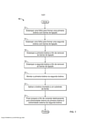
[008] Figura 1 é um diagrama que mostra as etapas de processamento para a fabricação de uma bobina de carregador sem fio;[008] Figure 1 is a diagram showing the processing steps for manufacturing a wireless charger coil;
[009] Figura 2 é uma vista esquemática de uma primeira bobina estampada com barras de ligação;[009] Figure 2 is a schematic view of a first stamped coil with connecting bars;
[0010] Figura 3 é uma vista esquemática de uma segunda bobina estampada com barras de ligação;[0010] Figure 3 is a schematic view of a second coil stamped with connecting bars;
[0011] Figura 4 é uma vista esquemática de uma bobina montada depois de as barras de ligação da primeira e segunda bobinas estampadas serem removidas;[0011] Figure 4 is a schematic view of an assembled coil after the tie bars of the first and second stamped coils are removed;
[0012] Figura 5 é uma vista esquemática da bobina de carregador sem fio montada com jumpers fixados;[0012] Figure 5 is a schematic view of the wireless charger coil assembled with jumpers attached;
[0013] Figura 6 é uma vista ampliada da porção A da Figura 5;[0013] Figure 6 is an enlarged view of portion A of Figure 5;
[0014] Figura 7 é uma vista esquemática de um conjunto de componentes elétricos incluindo uma bobina de carregador sem fio e uma antena NFC (de comunicação de campo próximo);[0014] Figure 7 is a schematic view of a set of electrical components including a wireless charger coil and an NFC (near field communication) antenna;
[0015] Figura 8 é uma vista esquemática de uma bobina de carregador sem fio montada com bobinas bifilares planas;[0015] Figure 8 is a schematic view of a wireless charger coil assembled with flat bifilar coils;
[0016] Figura 9 é uma vista em seção transversal de uma porção da bobina de carregador sem fio da Figura 8;[0016] Figure 9 is a cross-sectional view of a portion of the wireless charger coil of Figure 8;
[0017] Figura 10 é uma vista esquemática de uma bobina de carregador sem fio montada com bobinas bifilares empilhadas;[0017] Figure 10 is a schematic view of a wireless charger coil assembled with stacked bifilar coils;
[0018] Figura 11 é uma vista em seção transversal de uma porção da bobina de carregador sem fio da Figura 10;[0018] Figure 11 is a cross-sectional view of a portion of the wireless charger coil of Figure 10;
[0019] Figura 12 é uma vista em perspectiva de um conjunto de componentes elétricos;[0019] Figure 12 is a perspective view of a set of electrical components;
[0020] Figura 13 é uma vista explodida do conjunto de componentes elétricos da Figura 12;[0020] Figure 13 is an exploded view of the set of electrical components of Figure 12;
[0021] Figura 14 é uma vista em perspectiva de uma bobina ressonante;[0021] Figure 14 is a perspective view of a resonant coil;
[0022] Figura 15 é uma vista em perspectiva de um conjunto de bobinas ressonantes;[0022] Figure 15 is a perspective view of a set of resonant coils;
[0023] Figura 16 é uma vista em perspectiva de uma bobina ressonante estampada dobrada;[0023] Figure 16 is a perspective view of a folded stamped resonant coil;
[0024] Figura 17 é uma vista em perspectiva da bobina da Figura 16 parcialmente aberta;[0024] Figure 17 is a perspective view of the coil of Figure 16 partially opened;
[0025] Figura 18 é uma vista em perspectiva da bobina da Figura 16 totalmente aberta;[0025] Figure 18 is a perspective view of the coil of Figure 16 fully open;
[0026] Figura 19 é uma vista explodida de um conjunto de componentes elétricos em perfil baixo; e[0026] Figure 19 is an exploded view of a set of electrical components in low profile; and
[0027] Figura 20 é uma vista em perspectiva do material de enchimento da Figura 19;[0027] Figure 20 is a perspective view of the filler of Figure 19;
[0028] Figura 21 é um diagrama que mostra as etapas de processamento para a fabricação de uma bobina de carregador sem fio com adesivo;[0028] Figure 21 is a diagram showing the processing steps for manufacturing a wireless charger coil with adhesive;
[0029] Figura 22 é uma vista em seção transversal parcial de uma primeira bobina estampada quando aplicada a um primeiro laminado;[0029] Figure 22 is a partial cross-sectional view of a first stamped coil when applied to a first laminate;
[0030] Figura 23 é uma vista em seção transversal parcial de uma bobina montada posicionada entre um primeiro e segundo laminados;[0030] Figure 23 is a partial cross-sectional view of an assembled coil positioned between a first and second laminate;
[0031] Figura 24 é uma vista em seção transversal parcial de uma bobina montada;[0031] Figure 24 is a partial cross-sectional view of an assembled coil;
[0032] Figura 25 é uma vista de topo parcial da bobina montada da Figura 24;[0032] Figure 25 is a partial top view of the assembled coil of Figure 24;
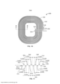
[0033] Figura 26 é uma vista de topo de uma bobina montada da presente invenção;[0033] Figure 26 is a top view of an assembled coil of the present invention;
[0034] Figura 27 é uma vista em perspectiva do conjunto de bobinas de carregador sem fio;[0034] Figure 27 is a perspective view of the wireless charger coil assembly;
[0035] Figura 28 é uma vista frontal do conjunto de bobinas de carregador sem fio da Figura 27;[0035] Figure 28 is a front view of the wireless charger coil assembly of Figure 27;
[0036] Figura 29 é uma vista lateral do conjunto de bobinas de carregador sem fio da Figura 27;[0036] Figure 29 is a side view of the wireless charger coil assembly of Figure 27;
[0037] Figura 30 é uma vista ampliada da Área 30-30 da Figura 29;[0037] Figure 30 is an enlarged view of Area 30-30 of Figure 29;
[0038] Figura 31 é uma vista explodida do conjunto de bobinas de carregador sem fio da Figura 27;[0038] Figure 31 is an exploded view of the wireless charger coil assembly of Figure 27;
[0039] Figura 32 é uma vista frontal de uma bobina do conjunto de bobinas de carregador sem fio da Figura 27; e[0039] Figure 32 is a front view of a coil of the wireless charger coil assembly of Figure 27; and
[0040] Figura 33 é uma vista frontal de um filme do conjunto de bobinas de carregador sem fio da Figura 27.[0040] Figure 33 is a front view of a film of the wireless charger reel assembly of Figure 27.
[0041] A presente invenção se refere a uma bobina de carregador sem fio e a métodos de produção da mesma. Tal como descrito em mais detalhe abaixo com relação às Figuras 1 a 7, a bobina de carregador sem fio estampada metálica compreende uma série de traços paralelos conectados de uma maneira bifilar. Em outras palavras, a bobina de carregador sem fio inclui uma primeira e uma segunda bobinas paralelas, estreitamente espaçadas, e conectadas em série de tal modo que a primeira e a segunda bobinas tenham correntes paralelas. A primeira e a segunda bobinas podem ser empilhadas ou conectadas planas ou conectadas em série e/ou paralelas a fim de atender a exigências de desempenho (por exemplo, requisitos elétricos, requisitos de energia, etc.). A bobina de carregador sem fio poderá ser usada em qualquer dispositivo energizado à bateria, particularmente em dispositivos móveis (por exemplo, smartfones, computadores do tipo tablet, relógios, etc.). A bobina de carregador sem fio pode ser produzida de modo a ser compatível com o padrão Qi, mas também poderá ser ajustada de modo a atender a qualquer outro protocolo de transferência sem fio. Uma bobina de carregador sem fio com uma quantidade maior de material condutivo, tal como cobre, pode ser posicionada dentro de um determinado espaço ao variar (por exemplo, aumentando) a espessura da bobina, o que aumentará a disponibilidade de energia. Em comparação com outras bobinas de carregador sem fio, as bobinas de carregador sem fio descritas no presente documento exibem uma maior efetividade de acoplamento magnético (por exemplo, uma maior força de campo magnético) e, desta maneira, transmitir energia com mais eficiência.[0041] The present invention relates to a wireless charger coil and methods of producing the same. As described in more detail below with respect to Figures 1 to 7, the metallic stamped wireless charger coil comprises a series of parallel traces connected in a bifilar fashion. In other words, the wireless charger coil includes first and second closely spaced parallel coils and connected in series such that the first and second coils carry parallel currents. The first and second coils can be stacked or connected flat or connected in series and/or parallel to meet performance requirements (eg electrical requirements, power requirements, etc.). The wireless charger coil can be used in any battery-powered device, particularly mobile devices (eg smartphones, tablet computers, watches, etc.). The wireless charger coil can be produced to conform to the Qi standard, but it can also be adjusted to meet any other wireless transfer protocol. A wireless charger coil with a larger amount of conductive material, such as copper, can be positioned within a certain space by varying (eg, increasing) the thickness of the coil, which will increase power availability. As compared to other wireless charger coils, the wireless charger coils described herein exhibit greater magnetic coupling effectiveness (eg, greater magnetic field strength) and thus transmit power more efficiently.
[0042] A Figura 1 é um diagrama que mostra as etapas de processamento 10 para a fabricação de uma bobina de carregador sem fio da presente invenção. De acordo com a etapa 12, uma folha de metal é estampada de modo a formar uma primeira bobina com barras de ligação. A folha de metal poderá ser qualquer uma dentre uma variedade de materiais adequados para uma transferência de energia sem fio (por exemplo, cobre, liga de cobre, alumínio, liga de alumínio, etc.). De acordo com a etapa 14, uma folha de metal (por exemplo, a mesma folha de metal ou uma folha de metal diferente) é estampada de modo a formar uma segunda bobina com barras de ligação. De acordo com a etapa 16, a primeira bobina é estampada a fim de remover as barras de ligação. De acordo com a etapa 18, a segunda bobina é estampada a fim de remover as barras de ligação. De acordo com a etapa 20, a primeira e a segunda bobinas são montadas juntas. De acordo com a etapa 22, a bobina montada é aplicada a um substrato de ferrite. De acordo com a etapa 24, jumpers (por exemplo, cabos) são fixados de modo a conectar eletricamente uma primeira e uma segunda bobinas em série (por exemplo, uma extremidade interna da primeira bobina é eletricamente conectada à extremidade externa da segunda bobina através de um jumper).[0042] Figure 1 is a diagram showing 10 processing steps for manufacturing a wireless charger coil of the present invention. According to step 12, a sheet of metal is stamped to form a first coil with connecting bars. The metal foil may be any of a variety of materials suitable for wireless energy transfer (e.g. copper, copper alloy, aluminum, aluminum alloy, etc.). According to step 14, a sheet of metal (e.g. the same sheet of metal or a different sheet of metal) is stamped to form a second coil with connecting bars. According to step 16, the first coil is stamped in order to remove the tie bars. According to step 18, the second coil is stamped in order to remove the tie bars. According to step 20, the first and second coils are assembled together. According to step 22, the assembled coil is applied to a ferrite substrate. According to step 24, jumpers (e.g. cables) are fixed to electrically connect a first and a second coil in series (e.g. an inner end of the first coil is electrically connected to the outer end of the second coil via a jumper).
[0043] As etapas acima descritas poderão ser trocadas, consolidadas, ou totalmente omitidas. Por exemplo, as bobinas podem ser estampadas sem primeiramente formar as barras de ligação, e/ou a primeira e a segunda bobinas poderão ser aplicadas diretamente ao ferrite (sem que tenham sido primeiramente montadas), etc. Além disso, a bobina poderá ser gravada ou usinada fotoquimicamente, ao invés de estampada, ou poderá ainda feita por meio de qualquer outro processo de fabricação adequado.[0043] The steps described above may be exchanged, consolidated, or omitted entirely. For example, coils can be stamped without first forming the tie bars, and/or the first and second coils can be applied directly to the ferrite (without first being assembled), etc. In addition, the coil may be photochemically engraved or machined, rather than stamped, or made using any other suitable manufacturing process.
[0044] A Figura 2 é uma vista de uma primeira bobina estampada 30 com barras de ligação. A primeira bobina 30 pode ser um traço em espiral de modo geral retangular planar 31, embora o traço 31 possa ter qualquer outro formato (por exemplo, uma espiral circular planar). As dimensões da bobina 30 podem variar dependendo da aplicação da bobina 30 (por exemplo, tal quando usada nos dispositivos móveis, nos dispositivos vestíveis, nos automóveis, etc.). A bobina 30 pode ser de qualquer espessura adequada, tal como entre 0,003 polegada e 0,020 polegada, etc., mas poderá ser mais grossa para aplicações de maior força. A bobina 30 pode ser de quaisquer dimensões gerais adequadas, tal como entre 0,25 polegada e 4 polegadas de largura e/ou entre 0,25 polegada e 4 polegadas de altura. O traço 31 poderá também ser quaisquer dimensões adequadas. Por exemplo, o traço 31 poderá ter entre 0,005 polegada e 0,250 polegada de largura. As dimensões poderão variar dependendo das necessidades físicas ou de desempenho do dispositivo móvel (por exemplo, uma requerida frequência). A bobina 30 pode ser feita de qualquer material adequado para uma transferência de energia sem fio, tal como, por exemplo, cobre, liga de cobre, alumínio, liga de alumínio, liga de cobre temperado (por exemplo, C110), etc.[0044] Figure 2 is a view of a first stamped
[0045] O traço 31 da bobina 30 dá voltas em torno de um centro qualquer número de vezes (por exemplo, 5, 10, etc.), de tal modo a atender quaisquer necessidades de energia indutiva ou ressonante. O traço 31 faz uma espiral de modo a formar uma porção interna 32 no centro da bobina 30. Como resultado, a bobina 30 terá uma extremidade interna 34 e uma extremidade externa 36. Os espaços 38 entre os traços 31 são configurados de modo a ser grandes o suficiente (por exemplo, de 0,0285 polegada) para acomodar a segunda bobina estampada (descrita em mais detalhe abaixo). As barras de ligação 40 podem ser posicionadas em uma pluralidade de locais ao longo desses espaços 38 de modo a manter a forma geral da bobina 30 (por exemplo, impedir o desenrolamento ou a deformação da forma), tal como durante o transporte da bobina 30 entre locais ou entre estações. A extremidade externa 36 pode se estender para fora em um ângulo, tal como, um ângulo de modo geral de noventa graus. A extremidade interna 34 e a extremidade externa 36 podem ser dispostas na direção do mesmo lado da bobina 30, mas poderão também ser dispostas em qualquer uma dentre uma variedade de posições na bobina 30.[0045]
[0046] A Figura 3 é uma vista de uma segunda bobina estampada 50 com barras de ligação. A segunda bobina 50 compartilha a maior parte das características e aspectos da primeira bobina tal como mostrada na Figura 2. A segunda bobina 50 pode ser um traço em espiral de modo geral retangular planar 51, embora o traço 51 possa ser de qualquer formato adequado (por exemplo, uma espiral circular planar). As dimensões da bobina 50 podem variar dependendo da aplicação da bobina 50 (por exemplo, tal como usada nos dispositivos móveis, nos dispositivos vestíveis, nos automóveis, etc.). A bobina 50 pode ser de qualquer espessura adequada, tal como entre 0,003 polegada e 0,020 polegada, etc., mas poderá também ser mais grossa para aplicações de maior força. A bobina 50 poderá ser de quaisquer dimensões gerais adequadas, tais como entre 0,25 polegada e 4 polegadas de largura e/ou entre 0,25 polegada e 4 polegadas de altura. O traço 51 pode ser também de quaisquer dimensões adequadas. Por exemplo, o traço 51 poderá ter entre 0,005 polegada e 0,250 polegada de largura. As dimensões podem variar dependendo das necessidades físicas ou de desempenho do dispositivo móvel (por exemplo, uma requerida frequência). A bobina 50 pode ser feita de qualquer material adequado para uma transferência de energia sem fio, tal como, por exemplo, cobre, liga de cobre, alumínio, liga de alumínio, liga de cobre temperado (por exemplo, C110), etc.[0046] Figure 3 is a view of a second stamped
[0047] O traço 51 da bobina 50 dá voltas ao redor de um centro qualquer número de vezes (por exemplo, 5, 10, etc.), de tal modo a atender quaisquer necessidades de energia indutiva ou ressonante. O traço 51 faz uma espiral de modo a formar uma porção interna 52 no centro da bobina 50. Como resultado, a bobina 50 terá uma extremidade interna 54 e uma extremidade externa 56. Os espaços 58 entre os traços 51 são configurados de modo a ser grandes o suficiente (por exemplo, de 0,0285 polegada) para acomodar a primeira bobina estampada 30 (acima descrita). As barras de ligação 60 podem ser posicionadas em uma pluralidade de locais ao longo desses espaços 58 de modo a manter a forma geral da bobina 50 (por exemplo, impedir o desenrolamento ou a deformação da forma), tal como durante o transporte da bobina 50 entre locais ou entre estações. A extremidade externa 56 não se estende para fora tal como a primeira bobina 30 (mas poderia). A extremidade interna 54 e a extremidade externa 56 podem ser dispostas na direção do mesmo lado da bobina 50, mas poderão também ser dispostas em qualquer uma dentre uma variedade de posições na bobina 50.[0047]
[0048] A Figura 4 é uma vista de uma bobina montada 170 depois de as barras de ligação da primeira e segunda bobinas estampadas 130, 150 serem removidas. Tal como mostrado, a primeira e a segunda bobinas 130, 150 se encaixam uma na outra. Em termos mais específicos, a primeira bobina 130 se encaixa no espaço formado entre os traços 151 da segunda bobina 150, e, em contrapartida, a segunda bobina 150 se encaixa no espaço formado entre os traços 131 da primeira bobina 130. No entanto, quando montadas, haverá pequenas aberturas entre os traços 131 da primeira bobina 130 e os traços 151 da segunda bobina 150 (por exemplo, de 0,003 polegada, 0,004 polegada, etc.), tal como descrito abaixo em mais detalhe. Como resultado, em conjunto a primeira e a segunda bobinas 130, 150 formarão uma espiral paralela planar. Também tal como mostrado, a extremidade interna 134 da primeira bobina 130 fica adjacente à extremidade interna 154 da segunda bobina 150, e a extremidade externa 136 da primeira bobina 130 fica adjacente à extremidade externa 156 da segunda bobina 150. No entanto, as extremidades poderão ficar a qualquer distância relativa uma da outra. Esse método de estampagem pode apresentar uma variação de largura de espaço médio de pelo menos aproximadamente 0,003 polegada para a bobina montada 170. A variância máxima e mínima dependerá das dimensões da bobina montada 170 (por exemplo, sua altura e largura gerais).[0048] Figure 4 is a view of an assembled
[0049] As tolerâncias limitadas e o formato em seção transversal retangular dos traços 130, 131 poderão resultar em uma razão de enchimento (de, por exemplo, 85 %) maior que a das atuais bobinas industriais (de, por exemplo, 65 %), tais como as bobinas enroladas, as bobinas gravadas, etc. Por exemplo, o formato em seção transversal retangular obtido a partir de uma estampagem (vide Figura 9 abaixo) provê uma razão de enchimento potencialmente maior que no formato em seção transversal circular de um fio redondo (por exemplo, um fio de cobre redondo). Em termos mais específicos, um fio redondo isolado de um diâmetro de 0,010 polegada (um fio de um diâmetro de 0,009 polegada com um isolamento de 0,0005 polegada) poderá prover uma razão de enchimento de 65 %, em comparação com uma bobina estampada com uma seção transversal retangular de 0,006 polegada de espessura e uma abertura de espaçamento de 0,003 polegada. Além disso, a bobina de carregador sem fio 170 pode operar em temperaturas ambientes mais elevadas do que outros fios industriais atuais (por exemplo, o fio Litz), e não é suscetível à degradação por vibração, choque, ou calor. Isso se deve em parte ao fato de a bobina de carregador sem fio 170 ser feita de um único condutor monolítico (e não, por exemplo, de um fio de multifilamentos). Esse poderá ser comparado aos filamentos individuais de um fio Litz, que tem um material de isolamento que separa cada um dos filamentos de fio individuais que não conseguem suportar altas temperaturas.[0049] The limited tolerances and rectangular cross-sectional shape of
[0050] A Figura 5 é uma vista da bobina de carregador sem fio montada 270 com jumpers fixados. Embora não mostrado, um jumper poderá ser fixado à primeira extremidade externa 236. Tal como mostrado, a extremidade interna 234 da primeira bobina 230 é eletricamente conectada à extremidade externa 256 da segunda bobina 250 por meio de um primeiro jumper 274. Essas extremidades 234, 256 ficam relativamente próximas uma à outra, e dispostas no mesmo lado da bobina 270 de modo a permitir um jumper curto 274. Um segundo jumper 276, nesse caso, será usado a fim de conectar a extremidade interna 254 da segunda bobina ao circuito do dispositivo móvel. A extremidade externa 236 e a extremidade interna 254 ficam relativamente próximas e dispostas na direção do mesmo lado da bobina 270 a fim de prover um jumper curto 276 e facilitar a fiação elétrica no dispositivo eletrônico. O resultado será um par de bobinas paralelas, proximamente espaçadas 230, 250 conectadas em série de tal modo que o primeiro e o segundo traços 230, 250 tenham correntes paralelas (por exemplo, as correntes de cada traço ficam no mesmo sentido horário ou anti-horário).[0050] Figure 5 is a view of the assembled
[0051] Quando totalmente montada com os demais componentes do dispositivo eletrônico, a porção interna 272 da bobina montada 270 fica isolada (por exemplo, por um plástico ou cola) de modo a garantir um desempenho apropriado. A bobina de carregador sem fio montada 270 poderá ter qualquer número de enrolamentos, dependendo das exigências elétricas. A bobina de carregador sem fio 270 pode ser usada em qualquer dispositivo que funciona à bateria, tal como os smartfones. A bobina montada 270 poderá ser de quaisquer dimensões gerais adequadas (por exemplo, uma largura de 1,142 polegadas e uma altura de 1,457 polegadas, etc.). O comprimento da bobina poderá ser de qualquer também adequado (por exemplo, de 48,459 polegadas).[0051] When fully assembled with the other components of the electronic device, the
[0052] A Figura 6 é uma vista ampliada da porção A da Figura 5. Tal como mostrado, existem aberturas muito pequenas 278 (por exemplo, vãos) entre os traços 231 da primeira bobina 230 e os traços 251 da segunda bobina 250 (por exemplo, de 0,003 polegada, 0,004 polegada, etc.), embora possam existir aberturas maiores 280 nos cantos de modo a incorporar as curvas dos traços 231, 251 (por exemplo, de tal modo que o aumento da abertura seja alternado). Essas tolerâncias limitadas poderão resultar em uma razão de enchimento maior que a dos atuais métodos industriais.[0052] Figure 6 is an enlarged view of portion A of Figure 5. As shown, there are very small openings 278 (e.g. gaps) between
[0053] A bobina de carregador sem fio montada 270 pode prover resistência (ohms) de corrente contínua (DC), resistência de corrente alternada (AC), e/ou razões de resistência de corrente AC/DC em uma quantidade de diferentes valores dependendo das dimensões da bobina de carregador 270 e do(s) material (materiais) usado(s) na construção da bobina de carregador. Os valores podem ser ajustados de modo a alcançar altas razões de corrente AC/DC a fim de atender os padrões de indução. As dimensões da bobina podem variar de modo a obter uma variação de resistência dependendo das requeridas características de desempenho. Por exemplo, para uma resistência de 0,232 ohms usando uma liga de C110, os traços 230, 250 poderão ter uma seção transversal de 0,0001234 polegada quadrada (por exemplo, uma espessura de 0,005 polegada e uma largura de 0,0246 polegada, ou uma espessura de 0,004 polegada e uma largura de 0,0308 polegada, etc.), e para uma resistência de 0,300 ohms usando uma liga de C110, os traços 230, 250 poderão ter uma seção transversal de 0,0000953 polegada quadrada (por exemplo, uma espessura de 0,005 polegada e uma largura de 0,019 polegada, ou uma espessura de 0,004 polegada e uma largura de 0,0238 polegada, etc.). A bobina de carregador sem fio estampada 270 poderá ter uma alta espessura de traço e/ou uma alta razão de aspecto high geral em comparação com outros métodos industriais atuais (por exemplo, as bobinas gravadas na placa de circuito impresso (PCB)).[0053] Mounted
[0054] A Figura 7 é uma vista de um conjunto de componentes elétricos 390 incluindo uma bobina de carregador sem fio 370. Em termos mais específicos, a bobina de carregador sem fio 370 é fixada a um substrato de ferrite 392 e em conjunto com uma antena de comunicação de campo próximo (NFC) 394 dotada de pás de contato. A bobina de carregador sem fio 370 e a antena NFC 394 podem ter pás de contato (por exemplo, douradas) a fim de conectar a bobina de carregador sem fio 370 e a antena NFC 394 ao circuito do dispositivo móvel. O conjunto compreende um primeiro jumper 374, um segundo jumper 376, e um terceiro jumper 377 que conectam as várias extremidades da bobina 370, tal como explicado em mais detalhe acima. Poderá ter um filme (por exemplo, um plástico transparente) sobre a bobina de carregador sem fio 370 e a antena NFC 394, com os jumpers 374, 376, 377 no topo do filme e atravessando o filme apenas nos pontos de conexão. Isso impedirá o curto acidental de qualquer uma das conexões elétricas da bobina 370. De maneira alternativa, os jumpers 374, 376, 377 poderão ficar isolados de tal maneira que um filme não seja necessário. A fim de minimizar espaço, a bobina de carregador sem fio 370 fica dentro da antena NFC 394 com os jumpers 376, 377 que se estendem para fora da antena NFC 394. No entanto, a bobina de carregador sem fio 370 e os jumpers 376, 377 poderão também ser colocados em qualquer local com relação à antena NFC 394.[0054] Figure 7 is a view of an assembly of
[0055] A espessura total do conjunto pode variar dependendo de várias necessidades e exigências potenciais. Por exemplo, os jumpers podem ser de 0,05 a 0,08 mm de espessura, o filme pode ser de 0,03 mm de espessura, a antena NFC 394 e a bobina 370 podem ser de 0,08 mm de espessura, e o ferrite 392 pode ser de 0,2 mm de espessura para uma espessura total de bobina de carregador sem fio de aproximadamente 0,36 mm.[0055] The total thickness of the assembly may vary depending on various needs and potential requirements. For example, the jumpers can be 0.05 to 0.08 mm thick, the film can be 0.03 mm thick, the
[0056] A Figura 8 é uma vista esquemática de uma bobina de carregador sem fio montada 470 com bobinas bifilares planas. Tal como acima descrito, a bobina de carregador sem fio 470 inclui uma primeira bobina 430 (por exemplo, um traço) e uma segunda bobina 450 (por exemplo, um traço). A bobina montada 470 é fabricada e opera da maneira acima apresentada com relação às Figuras 1 a 7. A primeira bobina 430 e a segunda bobina 450 podem ter qualquer espessura desejada, de tal modo a atender a diferentes exigências de energia. A primeira bobina 430 e a segunda bobina 450 podem ser conectadas em série ou em paralelo.[0056] Figure 8 is a schematic view of an assembled
[0057] A largura da primeira e/ou da segunda bobina 430, 450 pode variar ao longo do comprimento da bobina no sentido de otimizar o desempenho da bobina de carregador sem fio montada 470. De maneira alternativa, a espessura da primeira e da segunda bobinas 430, 450 pode mudar ao longo do comprimento da bobina. Por exemplo, a largura (e/ou espessura) da primeira bobina 430 pode aumentar (ou se estreitar) gradualmente de uma primeira extremidade 434 em direção ao meio da bobina 430, e a largura (e/ou espessura) poderá também gradualmente se estreitar (ou aumentar) do meio para a segunda extremidade 436 da bobina 430 (por exemplo, uma bobina espiral de um tipo larga-estreita-larga), deste modo variando toda a área em seção transversal. Qualquer variação de largura (por exemplo, em seção transversal) ou espessura poderá ser usada, e/ou essas dimensões poderão ser mantidas constantes ao longo de porções da bobina, de acordo com as desejadas características de desempenho.[0057] The width of the first and/or
[0058] Além disso, ou de maneira alternativa, os espaços entre os enrolamentos da bobina poderão variar no sentido de otimizar o desempenho da bobina de carregador sem fio 470. Por exemplo, a largura da abertura entre os traços poderá ser maior em direção ao lado de fora da primeira bobina 430 e mais estreita em direção ao lado de dentro da primeira bobina 430 (ou o contrário). De maneira similar, a distância entre a primeira bobina 430 e a segunda bobina 450 na bobina montada 470 poderá também variar no sentido de otimizar desempenho. Além disso, a geometria das bordas da bobina poderá variar (por exemplo, recortada, acastelada, etc.), de tal modo a reduzir correntes parasitas.[0058] In addition, or alternatively, the spaces between the coil windings may be varied in order to optimize the performance of the 470 Wireless Charger Coil. For example, the width of the gap between the traces may be wider towards the outside of the
[0059] A Figura 9 é uma vista em seção transversal de uma porção da bobina de carregador sem fio da Figura 8. A primeira bobina 430 compreende seções 414-424 e a segunda bobina 450 compreende seções 402-412. Tal como mostrado, a seção transversal da primeira bobina 430 se torna gradualmente mais larga e depois mais estreita de uma primeira extremidade para uma segunda extremidade da primeira bobina 430. Como resultado, as seções 414 e 424 são as mais estreitas (de, por exemplo, 0,025 polegada), seguidas das seções 404 e 422 (de, por exemplo, 0,030 polegada), e as seções 418 e 420 são as mais largas (de, por exemplo, 0,035 polegada). Da mesma forma, a seção transversal da segunda bobina 450 se torna gradualmente mais larga e depois mais estreita de uma primeira extremidade para uma segunda extremidade da segunda bobina 450. Como resultado, as seções 402 e 412 são as mais estreitas, e as seções 406 e 408 são as mais largas. Alterações nas dimensões da seção transversal antena poderão também ser feitas de diversas maneiras.[0059] Figure 9 is a cross-sectional view of a portion of the wireless charger coil of Figure 8. The
[0060] A Figura 10 é uma vista esquemática de uma bobina de carregador sem fio montada 570 com bobinas bifilares empilhadas. Tal como acima descrito, a bobina de carregador sem fio 570 inclui uma primeira bobina 530 e uma segunda bobina 550. A bobina montada 570 é fabricada e opera da maneira acima descrita com relação às Figuras 1 a 7, bem como tal como ilustrada nas Figuras 8 e 9, com exceção do fato de que a primeira e a segunda bobinas 530, 550 serem empilhadas ao invés de serem planas. A primeira bobina 530 inclui uma primeira extremidade 534 e uma segunda extremidade 536, e a segunda bobina 550 inclui uma primeira extremidade 554 e uma segunda extremidade 556. Além disso, uma variação na inclinação ou desvio (por exemplo, a distância de empilhamento) da primeira bobina 530 com relação à segunda bobina 550 poderá afetar o desempenho da bobina de carregador sem fio 570. A primeira bobina 530 e a segunda bobina 550 podem ser conectadas em série ou em paralelo.[0060] Figure 10 is a schematic view of an assembled
[0061] A Figura 11 é uma vista em seção transversal de uma porção da bobina de carregador sem fio da Figura 10. Essa bobina 570 é similar à das Figuras 8 e 9, incluindo uma primeira bobina 530 com seções 514 - 524 e uma segunda bobina 550 com seções 502 - 512, com exceção do fato de que a primeira e a segunda bobinas 530, 550 são empilhadas ao invés de planas.[0061] Figure 11 is a cross-sectional view of a portion of the wireless charger coil of Figure 10. This
[0062] As Figuras 12 e 13 são vistas que mostram um conjunto de componentes elétricos 690. Em termos mais específicos, a Figura 12 é uma vista em perspectiva de um conjunto de componentes elétricos 690. O conjunto de componentes elétricos 690 compreende um escudo de ferrite 692, uma camada de adesivo sensível à pressão (PSA) 602 posicionada sobre o escudo de ferrite 692, uma bobina montada 670 (por exemplo, uma bobina bifilar) posicionada entre as mesmas, e jumpers 674, 676 posicionados sobre a camada de adesivo PSA 602.[0062] Figures 12 and 13 are views showing an assembly of
[0063] A Figura 13 é uma vista explodida do conjunto de componentes elétricos 690 da Figura 12. A bobina bifilar 670 inclui uma primeira bobina 630 tendo uma extremidade interna 634 e uma extremidade externa 636 interconectada a uma segunda bobina 650 tendo uma extremidade interna 654 e uma extremidade externa 656. As extremidades internas e externas ficam no mesmo lado da bobina montada 670 a fim de facilitar seu uso e montagem (por exemplo, minimizar a distância para a conexão elétrica das extremidades).[0063] Figure 13 is an exploded view of the
[0064] O escudo de ferrite 692 inclui um primeiro furo 696 e um segundo furo 698 posicionados de modo a se correlacionarem com a colocação da extremidade interna 634 da primeira bobina 630 e da extremidade interna 654 da segunda bobina 650 (por exemplo, quando a bobina 670 é colocada sobre o escudo de ferrite 692). Embora os furos 696, 698 sejam mostrados como circulares, aberturas de qualquer formato e tamanho poderão ser feitas (por exemplo, uma abertura retangular, etc.). Esses furos 696, 698 facilitam a montagem e a soldagem do conjunto de componentes elétricos 690.[0064] The
[0065] A camada de adesivo PSA 602 e o escudo de ferrite 692 têm tamanhos similares entre si, e, embora mostrados como retangulares, tanto a camada como o escudo poderão ser de qualquer formato (por exemplo, circulares). A camada de adesivo PSA assegura a colocação relativa da bobina montada 670 no escudo de ferrite 692. A camada de PSA 602 pode ter adesivo em um ou em ambos os lados, e poderá incluir uma área de filme de politereftalato de etileno (PET) 604 livre de adesivo em um ou em ambos os lados. A área de filme de PET 604 facilita a montagem e soldagem do conjunto de componentes elétricos 690.[0065] The PSA
[0066] A camada de adesivo PSA 602 inclui um primeiro furo 606 e um segundo furo 608 na área de filme de PET 604 que se correlacionam em posição à colocação da extremidade interna 634 da primeira bobina 630 e da extremidade interna 654 da segunda bobina 650 (bem como ao primeiro furo 696 e ao segundo furo 698 do substrato de ferrite 692). Embora os furos 606, 608 sejam mostrados como circulares, aberturas de qualquer formato e tamanho poderão ser usadas (por exemplo, uma abertura retangular). Os furos 606, 608 provêem acesso através da camada de adesivo PSA 602 a fim de conectar eletricamente os jumpers 674, 676 às extremidades internas 634, 654 da bobina montada 670. A área de filme de PET 604 facilita a fixação dos jumpers 674, 676 no conjunto 690.[0066] The PSA
[0067] A Figura 14 é uma vista em perspectiva de uma bobina ressonante 730. A bobina ressonante 730 pode ser um traço em espiral de modo geral retangular planar 731, embora o traço 731 possa ter qualquer formato adequado. A bobina ressonante 730 inclui uma extremidade interna 734 e uma extremidade externa 736. O traço 731 é estampado sobre uma tira ou folha de metal (por exemplo, de cobre, alumínio, etc.). As dimensões da bobina 730 podem variar dependendo da aplicação da bobina 730. A bobina 730 poderá ser de qualquer espessura adequada, e de quaisquer dimensões gerais adequadas. O traço 731 poderá ser também de quaisquer dimensões adequadas. As dimensões podem variar de acordo com as exigências físicas e de desempenho. A bobina 730 pode ser feita de qualquer material adequado para uma transferência de energia sem fio, como, por exemplo, cobre, liga de cobre, alumínio, liga de alumínio, liga de cobre temperado (por exemplo, C110), etc. As aberturas entre os enrolamentos do traço 731 são maiores para uma bobina ressonante do que para outros tipos de bobinas indutivas devido às exigências de desempenho.[0067] Figure 14 is a perspective view of a
[0068] Uma estampagem provê um processo escalável a uma produção de alto volume com alta eficiência. O traço estampado 731 não é suscetível a desenrolamento e poderá permitir um traço mais grosso. Isso é vantajoso em comparação com outras tecnologias existentes. Por exemplo, enrolar um fio (por exemplo, de cobre) em um padrão específico sobre uma superfície é uma tarefa difícil e o fio enrolado pode se desenrolar. Além disso, o cobre gravado é caro e pode ficar limitado a uma espessura máxima (de, por exemplo, 0,004 polegada).[0068] A stamping provides a scalable process to high volume production with high efficiency.
[0069] O traço 731 da bobina ressonante 730 inclui um primeiro lado 737 e um segundo lado 739 deslocado do primeiro lado 737 por meio das porções anguladas 741 do traço 731. As porções anguladas 741 ficam alinhadas uma com relação à outra (por exemplo, ocorrem ao longo da linha B-B), e anguladas na mesma direção. Em outras palavras, as porções anguladas 741 são todas anguladas na direção de um lado em particular da bobina 730 (por exemplo, na direção de um lado da linha A-A), de tal modo que uma primeira porção 737 (por exemplo, a porção superior) da bobina 730 fique deslocada com relação a uma segunda porção 739 (por exemplo, a porção inferior) da bobina 730.[0069] The
[0070] A Figura 15 é uma vista em perspectiva de um conjunto de bobinas ressonantes 790, incluindo a primeira bobina ressonante 730 da Figura 14. O conjunto de bobinas ressonantes 790 inclui uma primeira bobina 730 e uma segunda bobina 750, as quais são idênticas uma à outra (o que minimiza custos de fabricação). O conjunto de bobinas ressonantes 790 pode ser laminado de tal modo que a primeira bobina 730 e a segunda bobina 750 sejam laminadas em um filme 702 (por exemplo, um filme de PET), tal como por meio de um adesivo (por exemplo, ativado por calor, sensível à pressão, etc.) de modo a prover mais estabilidade nas operações a jusante. A primeira bobina 730 pode ser aderida a um lado do filme 702 e a segunda bobina 750 pode ser aderida ao lado oposto do filme 702.[0070] Figure 15 is a perspective view of a
[0071] A primeira bobina 730 inclui uma extremidade externa 736 e uma extremidade interna 734, e a segunda bobina 750 inclui uma extremidade externa 756 e uma extremidade interna 754. A primeira bobina 730 e a segunda bobina 750 podem ser exatamente do mesmo tamanho e forma, com exceção do fato de que a segunda bobina 750 gira 180 graus em torno da linha D-D. Desta maneira, o traço 731 da primeira bobina 730 ficará posicionado entre a abertura formada pelos enrolamentos do traço 751 da segunda bobina 750 (ou vice versa), com exceção das porções anguladas de cada bobina ao longo da linha D-D, na qual os traços se cruzam entre si. A extremidade interna 734 da primeira bobina 730 pode ser adjacente à (ou ficar em conexão elétrica com a) extremidade interna 754 da segunda bobina 750, e a extremidade externa 736 da primeira bobina 730 pode ficar adjacente à extremidade externa 756 da segunda bobina 750.[0071] The
[0072] As Figuras 16 a 18 são vistas de uma bobina ressonante estampada 870. A Figura 16 é uma vista em perspectiva de uma bobina ressonante estampada dobrada 870. A bobina 870 compreende uma folha de conector 871, um primeiro conjunto de traços 831 de uma primeira porção de bobina 830 com suas extremidades conectadas a uma borda da folha de conector 871 nos pontos de conexão 873, e um segundo conjunto de traços 851 de uma segunda porção de bobina 850 com suas extremidades conectadas à mesma borda da folha de conector 871 nos pontos de conexão 873. A fim de criar a bobina ressonante estampada 870, uma (única) folha de metal é estampada de modo a formar o primeiro conjunto de traços 831 e o segundo conjunto de traços 851 (por exemplo, de tal modo que os arcos de cada traço do primeiro e segundo conjuntos de traços 831, 851 fiquem orientados na mesma direção). As extremidades do primeiro e segundo conjuntos de traços 831, 851 são, em seguida, conectadas à mesma borda da folha de conector 871 (por exemplo, um material isolante). A folha de conector 871 facilita a fiação dos conjuntos de traços 831, 851 um ao outro, bem como facilita a conexão da bobina ressonante estampada 870 ao circuito eletrônico. As extremidades do primeiro e segundo conjuntos de traços 831, 851 são, em seguida, cabeados um ao outro, tal como por meio do uso de uma série de jumpers e/ou traços. Por exemplo, os jumpers e/ou traços podem ficar na folha de conector 871 ou poderão trabalhar paralelos à folha de conector (ou perpendicular ao primeiro e segundo conjuntos de traços 831, 851).[0072] Figures 16 to 18 are views of a stamped
[0073] A Figura 17 é uma vista em perspectiva da bobina 870 da Figura 16 parcialmente aberta. Tal como mostrado, o primeiro conjunto de traços 831 da primeira porção de bobina 830 é curvado nos pontos de conexão 873. A Figura 18 é uma vista em perspectiva da bobina 870 da Figura 16 totalmente aberta. Tal como mostrado, o primeiro conjunto de traços 831 da primeira porção de bobina 830 continua a se curvar nos pontos de conexão 873 até que a primeira porção de bobina 830 fique planar à segunda porção de bobina 850. O curvamento dos traços poderá resultar na quebra da superfície externa dos mesmos, em cujo caso, uma solda ultrassônica poderá ser usada no sentido de garantir uma condutividade elétrica. De maneira alternativa, o primeiro e o segundo conjuntos de traços 831, 851 podem se conectar às bordas opostas da folha de conector 871, de tal modo que um encurvamento não se torne necessário. Uma estampagem (e encurvamento), desta maneira, reduzirá a quantidade de escória gerada e, por conseguinte, uma maior utilização de material.[0073] Figure 17 is a perspective view of the
[0074] A Figura 19 é uma vista explodida de um conjunto de componentes elétricos em perfil baixo 990. Em termos mais específicos, o conjunto de componentes elétricos em perfil baixo 990 compreende um substrato 992 (por exemplo, a camada de PET), uma camada de material de enchimento 933 (por exemplo, borracha, espuma, durômetro, etc.), uma bobina 930 (por exemplo, uma bobina ressonante), e uma camada de proteção 902. A camada de proteção 902 poderá ser parcialmente translúcida e poderá compreender uma aba (por exemplo, para aplicação ou remoção).[0074] Figure 19 is an exploded view of a low-profile
[0075] A Figura 20 é uma vista em perspectiva do material de enchimento 933 da Figura 19. O material de enchimento 933 compreende ranhuras 935 que correspondem em tamanho e formato à bobina 930. Desta maneira, a bobina 930 é encaixada no material de enchimento 933, o que impedirá que o formato da bobina possa se curvar e/ou sofrer deformação. Tal montagem facilita o manuseio da bobina 930 em operações subsequentes.[0075] Figure 20 is a perspective view of the
[0076] A Figura 21 é um diagrama que mostra as etapas de processamento 1000 para a fabricação de uma bobina de carregador sem fio com um adesivo (por exemplo, cola). De acordo com a etapa 1002, uma folha de metal é estampada de modo a formar uma primeira bobina com barras de ligação. De acordo com a etapa 1004, uma folha de metal é estampada de modo a formar uma segunda bobina com barras de ligação. De acordo com a etapa 1006, uma primeira bobina é aplicada a um primeiro laminado (por exemplo, plástico substrato, filme Transilwrap) com uma camada de adesivo de modo a aderir o mesmo. De acordo com a etapa 1008, uma segunda bobina é aplicada a um segundo laminado (por exemplo, plástico, substrato, filme Transilwrap) com uma camada de adesivo de modo a aderir o mesmo. De acordo com a etapa 1010, a primeira bobina é estampada a fim de remover as barras de ligação. De acordo com a etapa 1012, a segunda bobina é estampada a fim de remover as barras de ligação. Por conseguinte, a primeira bobina e a segunda bobina são fixadas no lugar como resultado da camada de adesivo sobre o laminado plástico. De acordo com a etapa 1014, a primeira bobina com o laminado aderido à mesma é montada na segunda bobina com o laminado aderido à mesma. Em termos mais específicos, tal como acima descrito, a primeira bobina com um traço em espiral se encaixa no espaço formado entre um traço de uma segunda bobina, e, em contrapartida, a segunda bobina se encaixa no espaço formado entre os traços da primeira bobina, desta maneira formando uma bobina montada. Como resultado, a bobina montada é posicionada entre (por exemplo, intercalada entre) o primeiro laminado e o segundo laminado.[0076] Figure 21 is a diagram showing 1000 processing steps for manufacturing a wireless charger coil with an adhesive (eg glue). According to
[0077] De acordo com a etapa 1016, uma prensa de calor é aplicada à bobina montada a fim de deslocar e definir a camada de adesivo dos primeiro e segundo laminados. Em termos mais específicos, o calor aplicado deve ser forte o suficiente para fundir o adesivo (por exemplo, maior que 104,44°C a 121,11°C (220°F a 250°F)), porém não suficiente para fundir o laminado de plástico. A pressão aplicada empurra a primeira bobina em direção ao segundo laminado, de tal modo que o adesivo do segundo laminado posicionado entre os traços da segunda bobina se desloque e seja forçado entre os espaços entre o primeiro traço da primeira bobina e o segundo traço da segunda bobina. A compressão da primeira e segunda bobinas juntas (por exemplo, com calor e/ou pressão) faz migrar o adesivo para os espaços entre os traços (por exemplo, de modo a isolar os mesmos um do outro). Essa compressão cobre ou reveste os traços da primeira bobina e da segunda bobina, e liga a primeira bobina à segunda bobina. A pressão, o calor, e a duração podem variar dependendo do tempo de ciclo desejado para a fabricação da bobina montada. Deve-se notar que tal processo poderá resultar em um desvio planar da primeira bobina da segunda bobina quando montadas juntas.[0077] According to
[0078] A Figura 22 é uma vista em seção transversal parcial de uma primeira bobina estampada 1130 quando aplicada a um primeiro laminado 1123. O primeiro laminado 1123 inclui uma camada de adesivo 1127 aplicada a uma superfície do mesmo. Quando a primeira bobina estampada 1130 é aplicada ao primeiro laminado 1123, uma certa quantidade do adesivo 1127 é deslocada para os lados, de tal modo que o adesivo deslocado 1127 se acumule contra os lados do traço 1131 da primeira bobina estampada 1130. Por conseguinte, o adesivo 1127 nos lados do e sob o traço 1131 da primeira bobina estampada 1130 impedirá que o traço 1131 se mova com relação ao primeiro laminado 1123.[0078] Figure 22 is a partial cross-sectional view of a first
[0079] A Figura 23 é uma vista em seção transversal parcial de uma bobina montada posicionada entre um primeiro laminado 1123 e um segundo laminado 1125. Tal como acima descrito, quando montada, a primeira bobina 1130 com um primeiro traço 1131 se encaixa no espaço formado entre um segundo traço 1151 de uma segunda bobina 1150, e, em contrapartida, a segunda bobina 1150 se encaixa no espaço formado entre o primeiro traço 1131 da primeira bobina 1130, desta maneira formando uma bobina montada 1170. Como resultado, a bobina montada 1170 fica posicionada entre (por exemplo, intercalada entre) o primeiro laminado 1123 e o segundo laminado 1125. Isso faz com que o primeiro adesivo 1127 se desloque entre o primeiro traço 1131 da primeira bobina 1130, e desloque o segundo adesivo 1129 entre o segundo traço 1151 da segunda bobina 1150.[0079] Figure 23 is a partial cross-sectional view of an assembled coil positioned between a
[0080] Quando a primeira e a segunda camadas de adesivo 1127, 1129 são definidas (por exemplo, por pressão e/ou calor), o adesivo irá cobrir a superfície dos traços 1131, 1151 (por exemplo, por soldagem), e atuará como um isolante e estabilizador para os traços 1131, 1151. Em outras palavras, a primeira e a segunda bobinas 1130, 1150 são ligadas entre si. Isso impedirá um movimento relativo dos traços 1131, 1151, o que impedirá que a primeira bobina estampada 1130 contate a segunda bobina estampada 1150 e avarie a bobina montada 1170. Como um exemplo, a primeira e segunda bobinas estampadas 1130, 1150 podem ser, cada qual, de 0,0125 polegada de espessura, e cada camada de adesivo 1127, 1129 poderá ter uma espessura de 0,0055 polegada, para uma espessura total de 0,0225 polegada. Depois de uma pressão e/ou calor ser aplicada, a espessura total poderá ser de 0,0205 polegada, com um deslocamento total do adesivo de 0,002 polegada.[0080] When the first and second layers of adhesive 1127, 1129 are set (e.g. by pressure and/or heat), the adhesive will cover the surface of
[0081] As Figuras 24 e 25 são vistas parciais de uma bobina montada 1170. Em termos mais específicos, a Figura 24 é uma vista em seção transversal parcial de uma bobina montada 1170, e a Figura 25 é uma vista de topo parcial da bobina montada 1170 da Figura 24. A bobina montada 1170 compreende (tal como acima descrito) uma primeira bobina 1130 com um traço em espiral 1131, que se encaixa no espaço formado entre um traço 1151 de uma segunda bobina 1150, e, em contrapartida, a segunda bobina 1150 se encaixa no espaço formado entre os traços 1131 da primeira bobina 1130. Por conseguinte, a primeira e a segunda bobinas 1130, 1150 formam uma espiral planar paralela.[0081] Figures 24 and 25 are partial views of an assembled
[0082] Tal como acima descrito, um primeiro laminado 1123 (por exemplo, um filme Transilwrap) com uma primeira camada de adesivo é aplicado à primeira bobina estampada 1130, e um segundo laminado 1125 (por exemplo, um filme Transilwrap) com uma segunda camada de adesivo é aplicado à segunda bobina estampada 1150. Como resultado, a primeira e a segunda bobinas estampadas 1130, 1150 ficam posicionadas entre o primeiro e o segundo laminados 1123, 1125. Quando a primeira e a segunda bobinas 1130, 1150 são montadas uma na outra, o adesivo 1127 (de cor preta, para fins de clareza) é deslocado a fim de encher os espaços entre o primeiro e o segundo traços 1131, 1151.[0082] As described above, a first laminate 1123 (e.g., a Transilwrap film) with a first layer of adhesive is applied to the first
[0083] A Figura 25 mostra o deslocamento do adesivo 1127 quando a primeira bobina 1130 e a segunda bobina 1150 são montadas. Em termos mais específicos, o adesivo 1127 (de cor preta para fins de clareza) é mostrado entre o primeiro traço 1131 e o segundo traço 1151. Além disso, tal como no exemplo mostrado em particular, uma pressão maior é exercida sobre o primeiro e segundo traços do lado esquerdo 1131a, 1151a, do que sobre os traços do lado direito 1131b, 1151b. Como resultado, uma quantidade menor de adesivo 1127 se desloca sobre o lado direito do que sobre o lado esquerdo, desta maneira tornando o traço do lado direito 1151b menos visível que o traço do lado esquerdo 1151a (como resultado do adesivo de cor preta 1127).[0083] Figure 25 shows the displacement of the adhesive 1127 when the
[0084] A Figura 26 é uma vista de topo de uma bobina montada 1270 da presente invenção. Tal como acima descrito, a bobina montada 1270 compreende uma primeira bobina 1230 com um primeiro traço em espiral 1231 tendo uma extremidade interna 1234 e uma extremidade externa 1236, uma segunda bobina 1250 com um segundo traço em espiral 1251 tendo uma extremidade interna 1254 e uma extremidade externa 1256, um primeiro jumper 1277 fixado à extremidade externa 1236 da primeira bobina 1230, um segundo jumper 1274 fixado à extremidade interna 1234 da primeira bobina 1230 e à extremidade externa 1256 da segunda bobina 1250, e um terceiro jumper 1276 fixado à extremidade interna 1254 da segunda bobina 1250. A primeira e segunda bobinas em espiral 1230, 1250 formando uma porção interna 1272.[0084] Figure 26 is a top view of an assembled
[0085] Um laminado 1227 (por exemplo, um filme, um filme adesivo, um filme plástico, etc.) cobre a bobina montada 1270, inclusive a porção interna 1272. Tal como acima explicado, a camada de adesivo do laminado 1227 estabiliza a primeira bobina 1230 e a segunda bobina 1250 e isola as mesmas. Isso impedirá o movimento relativo da primeira e segunda bobinas 1230, 1250 como também impedirá que a primeira e a segunda bobinas 1230, 1250 entre em contato acidentalmente uma com a outra, e avarie a bobina montada 1270.[0085] A laminate 1227 (e.g., a film, an adhesive film, a plastic film, etc.) covers the assembled
[0086] O laminado 1227 poderá definir um ou mais recortes. Em termos mais específicos, o laminado 1227 pode definir um recorte interno 1223 a fim de prover acesso à (por exemplo, expor a) primeira extremidade interna 1234 da primeira bobina 1230 e a segunda extremidade interna 1254 da segunda bobina 1250. O laminado 1227 poderá também definir um recorte externo 1225 a fim de prover acesso à (por exemplo, expor a) primeira extremidade externa 1236 da primeira bobina 1230 e a segunda extremidade externa 1256 da segunda bobina 1250. O primeiro recorte 1223 pode substancialmente se estender a partir da porção interna 1272. A bobina montada 1270 (e a primeira e a segunda bobinas 1230, 1250 da mesma) pode ser de qualquer material e/ou estilo (por exemplo, uma bobina do tipo A6).[0086]
[0087] As Figuras 27 a 33 ilustram um outro conjunto de bobinas de carregador sem fio 1300 da presente invenção. As Figuras 27 a 29 e 31 são, respectivamente, vistas em perspectiva, frontal, lateral, e explodida do conjunto de bobinas de carregador sem fio 1300. A Figura 30 é uma vista ampliada da Área 30-30 da Figura 29. O conjunto de bobinas de carregador sem fio 1300 inclui uma primeira bobina 1302a, uma segunda bobina 1302b, e um filme 1304.[0087] Figures 27 to 33 illustrate another set of
[0088] A Figura 32 é uma vista frontal da primeira e segunda bobinas 1302a, 1302b, as quais podem ser idênticas em estrutura a fim de minimizar custos de fabricação. A primeira e a segunda bobinas 1302a, 1302b incluem, cada uma das mesmas, uma extremidade interna 1306a, 1306b, uma extremidade externa 1308a, 1308b, e um traço 1310a, 1310b que se estende a partir da respectiva extremidade interna 1306a, 1306b para a respectiva extremidade externa 1308a, 1308b. As extremidades internas 1306a, 1306b da primeira e segunda bobinas 1302a, 1302b podem ser as primeiras porções dos respectivos traços 1310a, 1310b, enquanto que as extremidades externas 1308a, 1308b da primeira e segunda bobinas 1302a, 1302b podem ser as segundas porções dos respectivos traços 1310a, 1310b. As extremidades internas 1306a, 1306b podem ser formadas como uma aba mais larga que o traço, enquanto que as extremidades externas 1308a, 1308b podem ser formadas como abas alongadas. No que diz respeito a esse aspecto, as extremidades internas 1306a, 1306b poderão ter qualquer formato adequado, tal como um formato quadrado, enquanto que as extremidades externas 1308a, 1308b poderão ter qualquer formato adequado, tal como um formato retangular. A primeira e a segunda bobinas 1302a, 1302b são estampadas a partir de uma tira ou folha de metal, e podem ser feitas de qualquer material adequado para uma transferência de energia sem fio, tal como, por exemplo, cobre, liga de cobre, alumínio, liga de alumínio, liga de cobre temperado (por exemplo, C110), etc. As dimensões da primeira e a segunda bobinas 1302a, 1302b podem variar dependendo da aplicação do conjunto de bobinas de carregador sem fio 1300. Os traços 1310a, 1310b podem também ser de quaisquer dimensões adequadas dependendo das exigências físicas e de desempenho. A primeira e a segunda bobinas 1302a, 1302b podem ser exatamente do mesmo tamanho e formato, com a segunda bobina 1302b girando 180 graus quando o conjunto de bobinas de carregador sem fio 1300 é formado, tal como descrito em mais detalhe abaixo.[0088] Figure 32 is a front view of the first and
[0089] A Figura 33 é uma vista frontal do filme 1304. O filme 1304 pode ser um filme dielétrico fino que inclui um corpo 1312 que tem um primeiro lado 1314, um segundo lado 1316, uma abertura interna 1318, e uma abertura externa 1320. O primeiro lado e o segundo lado 1314, 1316 podem incluir um adesivo sobre os mesmos, cujo adesivo permitirá que cada primeira e segunda bobinas 1302a, 1302b fiquem presas em um dentre o primeiro lado ou o segundo lado 1314, 1316. A abertura interna 1318 se estende através do corpo 1312, por exemplo, do primeiro lado 1314 para o segundo lado 1316, e é dimensionada e formada de modo a corresponder ao tamanho e formato das extremidades internas 1306a, 1306b da primeira e segunda bobinas 1302a, 1302b. A abertura interna 1318 é posicionada no corpo 1312 de modo a se correlacionar com a colocação das extremidades internas 1306a, 1306b da primeira e segunda bobinas 1302a, 1302b, por exemplo, quando a primeira bobina 1302a é colocada no primeiro lado 1314 do filme 1304 e a segunda bobina 1302b é colocada no segundo lado 1316 do filme 1304. A abertura externa 1320 se estende através do corpo 1312, por exemplo, do primeiro lado 1314 para o segundo lado 1316, e é dimensionada e formada de modo a corresponder ao tamanho e formato das extremidades externas 1308a, 1308b da primeira e segunda bobinas 1302a, 1302b quando as extremidades externas 1308a, 1308b são posicionadas adjacentes uma à outra. Assim sendo, a abertura externa 1320 é posicionada no corpo 1312 de modo a se correlacionar com a colocação das extremidades externas 1308a, 1308b da primeira e segunda bobinas 1302a, 1302b, por exemplo, quando a primeira bobina 1302a é colocada no primeiro lado 1314 do filme 1304 e a segunda bobina 1302b é colocada no segundo lado 1316 do filme 1304. A abertura interna 1318 facilita a montagem e conexão elétrica (por exemplo, através de soldagem, brasagem forte, ligação elétrica, ou outro meio) do conjunto de bobinas de carregador sem fio 1300, e a abertura externa 1320 provê acesso às extremidades externas 1308a, 1308b da primeira e segunda bobinas 1302a, 1302b a partir de ambos os lados 1314, 1316 do filme 1304, por exemplo, as extremidades externas 1308a, 1308b podem ser contatadas por ou conectadas a um outro componente elétrico a partir de um dos ou de ambos os lados 1314, 1316 do filme 1304. Embora a abertura interna 1318 seja mostrada como quadrada, e a abertura externa 1320 seja mostrada como retangular, uma pessoa com conhecimento simples na técnica poderá entender que aberturas de qualquer tamanho e formato poderão ser utilizadas, contanto que as mesmas correspondam de modo geral ao formato das extremidades internas 1306a, 1306b das bobinas 1302a, 1302b (para a abertura interna 1318) e das extremidades externas 1308a, 1308b das bobinas 1302a, 1302b (para a abertura externa 1320).[0089] Figure 33 is a front view of
[0090] Tal como mostrado nas Figuras 27 a 31, o conjunto de bobinas de carregador sem fio 1300 é construído de tal maneira que a primeira bobina 1302a fique aderida ao primeiro lado 1314 do filme 1304, por exemplo, por meio de um adesivo no primeiro lado 1314, e que a segunda bobina 1302b fique aderida ao segundo lado 1316 do filme 1304, por exemplo, por meio de um adesivo no segundo lado 1316, porém girada 180 graus com relação à primeira bobina 1302a. Tal como mostrado nas Figuras 28 e 30, o filme 1312 se estende de modo geral para além da primeira e segunda bobinas 1302a, 1302b. A primeira bobina 1302a é aderida ao filme 1304 com a extremidade interna 1306a da mesma sendo posicionada adjacente à abertura interna 1318 do filme 1304, e com a extremidade externa 1308a da mesma sendo posicionada adjacente à abertura externa 1320 do filme 1304. A segunda bobina 1302b é aderida ao filme 1304 com a extremidade interna 1306b da mesma sendo posicionada adjacente à abertura interna 1318 do filme 1304 sobreposta à extremidade interna 1306a da primeira bobina 1302a, e com a extremidade externa 1308b da mesma sendo posicionada adjacente à abertura externa 1320 do filme 1304 adjacente à extremidade externa 1308a da primeira bobina 1302a. As extremidades internas 1306a, 1306b da primeira e segunda bobinas 1302a, 1302b são presas uma à outra (por exemplo, através de soldagem, brasagem forte, ligação elétrica, ou outro meio) de tal modo que as mesmas fiquem eletricamente conectadas e que a primeira e segunda bobinas 1302a, 1302b formem um único circuito. As extremidades externas 1308a, 1308b da primeira e segunda bobinas 1302a, 1302b são posicionadas adjacentes uma à outra na abertura externa 1320 de tal modo que as mesmas possam ser encaixadas a partir de ambos os lados do conjunto de bobinas de carregador sem fio 1300.[0090] As shown in Figures 27 to 31, the wireless
[0091] Para qualquer uma das modalidades acima descritas, a bobina de carregador sem fio (por exemplo, uma bobina bifilar) poderá ser construída e, em seguida, (por exemplo, em um local e/ou momento diferentes) a primeira e a segunda bobinas da bobina de carregador sem fio, quer sejam empilhadas ou planas, poderão ser eletricamente conectadas uma à outra em série ou em paralelo dependendo dos requisitos elétricos.[0091] For any of the above-described modalities, the wireless charger coil (e.g. a bifilar coil) may be constructed and then (e.g. at a different location and/or time) the first and second coils of the wireless charger coil, whether stacked or flat, can be electrically connected to each other in series or in parallel depending on electrical requirements.
[0092] Tendo, assim, descrito em detalhe o presente sistema e método, deve-se entender que o relatório descritivo acima não tem a intenção de limitar o seu espírito ou âmbito de aplicação. Deve-se entender que as modalidades da presente invenção aqui descritas são tão somente exemplares e que uma pessoa versada na técnica poderá fazer quaisquer variações ou modificações sem se afastar do espírito ou âmbito de aplicação da presente invenção. Todas essas variações e modificações, inclusive aquelas que se encontram descritas acima, foram concebidas de modo a serem incluídas ao âmbito de aplicação da presente invenção.[0092] Having thus described the present system and method in detail, it should be understood that the above descriptive report is not intended to limit its spirit or scope. It should be understood that the embodiments of the present invention described herein are exemplary only and that a person skilled in the art may make any variations or modifications without departing from the spirit or scope of the present invention. All such variations and modifications, including those described above, are designed to be included within the scope of the present invention.
Claims (16)
Applications Claiming Priority (7)
| Application Number | Priority Date | Filing Date | Title |
|---|---|---|---|
| US201361908573P | 2013-11-25 | 2013-11-25 | |
| US201462004587P | 2014-05-29 | 2014-05-29 | |
| US201462077721P | 2014-11-10 | 2014-11-10 | |
| US14/553,617 US9490656B2 (en) | 2013-11-25 | 2014-11-25 | Method of making a wireless charging coil |
| US15/854,197 | 2017-12-26 | ||
| US15/854,197 US10374464B2 (en) | 2013-11-25 | 2017-12-26 | Wireless charging coil |
| PCT/US2018/067197 WO2019133503A1 (en) | 2013-11-25 | 2018-12-21 | Wireless charging coil |
Publications (2)
| Publication Number | Publication Date |
|---|---|
| BR112020013056A2 BR112020013056A2 (en) | 2021-06-22 |
| BR112020013056B1 true BR112020013056B1 (en) | 2021-12-28 |
Family
ID=53182157
Family Applications (1)
| Application Number | Title | Priority Date | Filing Date |
|---|---|---|---|
| BR112020013056-7A BR112020013056B1 (en) | 2013-11-25 | 2018-12-21 | WIRELESS CHARGER COIL SET |
Country Status (7)
| Country | Link |
|---|---|
| US (5) | US9490656B2 (en) |
| EP (1) | EP3732697A4 (en) |
| JP (1) | JP6986636B2 (en) |
| KR (1) | KR102672445B1 (en) |
| CN (2) | CN114512310A (en) |
| BR (1) | BR112020013056B1 (en) |
| WO (1) | WO2019133503A1 (en) |
Families Citing this family (67)
| Publication number | Priority date | Publication date | Assignee | Title |
|---|---|---|---|---|
| US11476566B2 (en) | 2009-03-09 | 2022-10-18 | Nucurrent, Inc. | Multi-layer-multi-turn structure for high efficiency wireless communication |
| WO2013141658A1 (en) | 2012-03-23 | 2013-09-26 | 엘지이노텍 주식회사 | Antenna assembly and method for manufacturing same |
| TWI604480B (en) | 2012-03-23 | 2017-11-01 | Lg伊諾特股份有限公司 | Wireless power receiver and portable terminal comprising the same |
| JP6306288B2 (en) * | 2013-05-13 | 2018-04-04 | 日東電工株式会社 | Coil printed wiring board, power receiving module, battery unit and power receiving communication module |
| US9490656B2 (en) | 2013-11-25 | 2016-11-08 | A.K. Stamping Company, Inc. | Method of making a wireless charging coil |
| US9859052B2 (en) | 2013-11-25 | 2018-01-02 | A.K. Stamping Co., Inc. | Wireless charging coil |
| TW201539855A (en) * | 2014-04-11 | 2015-10-16 | Universal Scient Ind Co Ltd | Handheld device with multiple near field communication reading directions |
| US10333200B2 (en) * | 2015-02-17 | 2019-06-25 | Samsung Electronics Co., Ltd. | Portable device and near field communication chip |
| US10355528B2 (en) * | 2015-05-21 | 2019-07-16 | Aptiv Technologies Limited | Dual coil wireless power transmitter |
| US9991744B2 (en) * | 2015-07-03 | 2018-06-05 | Samsung Electro-Mechanics Co., Ltd. | Wireless power receiving device and apparatus including the same |
| KR101751121B1 (en) | 2015-07-16 | 2017-06-27 | 삼성전기주식회사 | Conductive plate and portable terminal having the same |
| US10658847B2 (en) * | 2015-08-07 | 2020-05-19 | Nucurrent, Inc. | Method of providing a single structure multi mode antenna for wireless power transmission using magnetic field coupling |
| US11205848B2 (en) * | 2015-08-07 | 2021-12-21 | Nucurrent, Inc. | Method of providing a single structure multi mode antenna having a unitary body construction for wireless power transmission using magnetic field coupling |
| US9960628B2 (en) | 2015-08-07 | 2018-05-01 | Nucurrent, Inc. | Single structure multi mode antenna having a single layer structure with coils on opposing sides for wireless power transmission using magnetic field coupling |
| US9941590B2 (en) * | 2015-08-07 | 2018-04-10 | Nucurrent, Inc. | Single structure multi mode antenna for wireless power transmission using magnetic field coupling having magnetic shielding |
| US9960629B2 (en) * | 2015-08-07 | 2018-05-01 | Nucurrent, Inc. | Method of operating a single structure multi mode antenna for wireless power transmission using magnetic field coupling |
| US10636563B2 (en) * | 2015-08-07 | 2020-04-28 | Nucurrent, Inc. | Method of fabricating a single structure multi mode antenna for wireless power transmission using magnetic field coupling |
| US10063100B2 (en) | 2015-08-07 | 2018-08-28 | Nucurrent, Inc. | Electrical system incorporating a single structure multimode antenna for wireless power transmission using magnetic field coupling |
| EP3657519A1 (en) * | 2015-08-07 | 2020-05-27 | NuCurrent, Inc. | Single layer multi mode antenna for wireless power transmission using magnetic field coupling |
| US9948129B2 (en) * | 2015-08-07 | 2018-04-17 | Nucurrent, Inc. | Single structure multi mode antenna for wireless power transmission using magnetic field coupling having an internal switch circuit |
| US9941729B2 (en) * | 2015-08-07 | 2018-04-10 | Nucurrent, Inc. | Single layer multi mode antenna for wireless power transmission using magnetic field coupling |
| US9941743B2 (en) * | 2015-08-07 | 2018-04-10 | Nucurrent, Inc. | Single structure multi mode antenna having a unitary body construction for wireless power transmission using magnetic field coupling |
| US10985465B2 (en) * | 2015-08-19 | 2021-04-20 | Nucurrent, Inc. | Multi-mode wireless antenna configurations |
| KR101967341B1 (en) | 2015-11-05 | 2019-08-13 | 엘지전자 주식회사 | Car Wireless Power Transmitters and Receivers |
| EP3504765A1 (en) | 2016-08-26 | 2019-07-03 | NuCurrent, Inc. | Wireless connector system |
| GB2553842B (en) * | 2016-09-16 | 2021-04-07 | Drayson Tech Europe Ltd | Three dimensional coil and method of making the same for inductive power transfer systems |
| EP3552298A4 (en) | 2016-12-09 | 2020-01-15 | NuCurrent, Inc. | SUBSTRATE WITH CONFIGURATION TO EASIER ENERGY TRANSFER THROUGH METAL THROUGH A MAGNETIC NEAR FIELD COUPLING |
| KR20180084307A (en) * | 2017-01-16 | 2018-07-25 | 엘지이노텍 주식회사 | Coil Device Of Apparatus For Transmitting And Receiving Wireless Power |
| US10903688B2 (en) | 2017-02-13 | 2021-01-26 | Nucurrent, Inc. | Wireless electrical energy transmission system with repeater |
| US11605487B2 (en) * | 2017-04-14 | 2023-03-14 | The Diller Corporation | Laminate with induction coils and charging station device comprising same |
| US11283295B2 (en) | 2017-05-26 | 2022-03-22 | Nucurrent, Inc. | Device orientation independent wireless transmission system |
| JP7056016B2 (en) * | 2017-06-13 | 2022-04-19 | Tdk株式会社 | Coil parts |
| EP3438996B1 (en) * | 2017-08-02 | 2021-09-22 | Ningbo Geely Automobile Research & Development Co., Ltd. | A device for a wireless power transfer system for a vehicle |
| TWD191614S (en) * | 2017-08-04 | 2018-07-11 | 合利億股份有限公司 | Wireless charger coil |
| JP6505820B1 (en) | 2017-12-18 | 2019-04-24 | 昭和電線ケーブルシステム株式会社 | Non-contact power feeder and coil |
| KR102505437B1 (en) * | 2017-12-26 | 2023-03-03 | 삼성전기주식회사 | Wire wound inductor and manufacturing method thereof |
| CN110033931B (en) * | 2018-01-12 | 2021-10-29 | 乾坤科技股份有限公司 | Electronic device and method of making the same |
| WO2019173579A1 (en) * | 2018-03-07 | 2019-09-12 | University Of Tennessee Research Foundation | Series self-resonant coil structure for conducting wireless power transfer |
| CN108565102B (en) * | 2018-03-28 | 2020-08-14 | 华为技术有限公司 | Coil module, wireless charging transmitting device, wireless charging receiving device, wireless charging system and wireless charging terminal |
| WO2019189760A1 (en) * | 2018-03-30 | 2019-10-03 | 大日本印刷株式会社 | Coil and coil pair, power transmission device and power receiving device, and power transmission system |
| CN111937272A (en) | 2018-04-19 | 2020-11-13 | 通用电气公司 | Receiver unit for wireless power transmission system |
| KR102469460B1 (en) | 2018-09-12 | 2022-11-22 | 멀티-파인라인 일렉트로닉스, 인코포레이티드 | balanced symmetrical coil |
| KR102622543B1 (en) * | 2018-09-19 | 2024-01-09 | 주식회사 위츠 | Coil assembly |
| TW202026824A (en) * | 2019-01-07 | 2020-07-16 | 哈帝斯科技股份有限公司 | Wireless charging mousepad structures and processes |
| JP1646786S (en) * | 2019-02-28 | 2019-12-02 | ||
| JP6546711B1 (en) * | 2019-04-10 | 2019-07-17 | 株式会社エスケーエレクトロニクス | Non-contact information carrier |
| CN111835043A (en) * | 2019-04-16 | 2020-10-27 | 致伸科技股份有限公司 | Wireless charging device and its transmitter module and transmitter coil |
| TWI687946B (en) * | 2019-04-16 | 2020-03-11 | 致伸科技股份有限公司 | Wireless charging device and transmitting module and transmitting coil thereof |
| US11380480B2 (en) | 2019-07-10 | 2022-07-05 | Lear Corporation | Strip induction coil for wireless charging of a vehicle battery |
| US11007887B2 (en) | 2019-07-11 | 2021-05-18 | Lear Corporation | Tubular induction coil for wireless charging of a vehicle battery |
| US11271430B2 (en) | 2019-07-19 | 2022-03-08 | Nucurrent, Inc. | Wireless power transfer system with extended wireless charging range |
| US11227712B2 (en) | 2019-07-19 | 2022-01-18 | Nucurrent, Inc. | Preemptive thermal mitigation for wireless power systems |
| US11056922B1 (en) | 2020-01-03 | 2021-07-06 | Nucurrent, Inc. | Wireless power transfer system for simultaneous transfer to multiple devices |
| US11923696B2 (en) | 2020-02-12 | 2024-03-05 | Google Llc | Passive adapter for magnetic inductive wireless charging |
| WO2021171204A1 (en) * | 2020-02-28 | 2021-09-02 | 3M Innovative Properties Company | Antenna for transfer of information or energy |
| US11283303B2 (en) | 2020-07-24 | 2022-03-22 | Nucurrent, Inc. | Area-apportioned wireless power antenna for maximized charging volume |
| US11417461B2 (en) * | 2020-10-29 | 2022-08-16 | Google Llc | Techniques and apparatuses to reduce inductive charging power loss |
| US11876386B2 (en) | 2020-12-22 | 2024-01-16 | Nucurrent, Inc. | Detection of foreign objects in large charging volume applications |
| US11881716B2 (en) | 2020-12-22 | 2024-01-23 | Nucurrent, Inc. | Ruggedized communication for wireless power systems in multi-device environments |
| US11695302B2 (en) | 2021-02-01 | 2023-07-04 | Nucurrent, Inc. | Segmented shielding for wide area wireless power transmitter |
| USD999166S1 (en) * | 2021-04-22 | 2023-09-19 | Fukushima Sic Applied Engineering Inc. | Power transformer |
| USD981958S1 (en) * | 2021-04-23 | 2023-03-28 | Fukushima Sic Applied Engineering Inc. | Coil for power transformer |
| CN113364144A (en) * | 2021-07-05 | 2021-09-07 | 浙江晶日科技股份有限公司 | Coil, wireless charging transmitting and receiving device and mobile terminal |
| KR102408962B1 (en) * | 2022-01-18 | 2022-06-22 | 주식회사 파인테크닉스 | Manufacturing method for wireless charging coil and wireless charging coil manufactured by the same |
| US11831174B2 (en) | 2022-03-01 | 2023-11-28 | Nucurrent, Inc. | Cross talk and interference mitigation in dual wireless power transmitter |
| US12003116B2 (en) | 2022-03-01 | 2024-06-04 | Nucurrent, Inc. | Wireless power transfer system for simultaneous transfer to multiple devices with cross talk and interference mitigation |
| CN117375265B (en) * | 2023-12-07 | 2024-03-26 | 清华大学深圳国际研究生院 | Self-resonant relay coil, wireless power transmission system and wireless charging system |
Family Cites Families (57)
| Publication number | Priority date | Publication date | Assignee | Title |
|---|---|---|---|---|
| US2645385A (en) * | 1949-10-28 | 1953-07-14 | Dearborn Motors Corp | Precision seed planter |
| US3214315A (en) | 1962-03-28 | 1965-10-26 | Burton Solomon | Method for forming stamped electrical circuits |
| US5142767A (en) | 1989-11-15 | 1992-09-01 | Bf Goodrich Company | Method of manufacturing a planar coil construction |
| JPH07220926A (en) * | 1994-02-08 | 1995-08-18 | Tokin Corp | Thin spiral coil part, coil element using said part & current transformer with coil element |
| JPH09213530A (en) | 1996-01-30 | 1997-08-15 | Alps Electric Co Ltd | Plane transformer |
| JPH09326736A (en) | 1996-06-03 | 1997-12-16 | Mitsubishi Electric Corp | Secondary side circuit equipment for wireless transmission/reception system and induction coil for wireless transmission/reception system |
| US5892425A (en) | 1997-04-10 | 1999-04-06 | Virginia Tech Intellectual Properties, Inc. | Interwound center-tapped spiral inductor |
| US5909050A (en) | 1997-09-15 | 1999-06-01 | Microchip Technology Incorporated | Combination inductive coil and integrated circuit semiconductor chip in a single lead frame package and method therefor |
| US6885275B1 (en) | 1998-11-12 | 2005-04-26 | Broadcom Corporation | Multi-track integrated spiral inductor |
| JP3680627B2 (en) * | 1999-04-27 | 2005-08-10 | 富士電機機器制御株式会社 | Noise filter |
| IL136301A (en) | 2000-05-22 | 2005-09-25 | Payton Planar Magnetics Ltd | Method of insulating a planar transformer printed circuit and lead frame windings forms |
| US7370403B1 (en) | 2000-06-06 | 2008-05-13 | Taiwan Semiconductor Manufacturing Co., Ltd. | Method of fabricating a planar spiral inductor structure having an enhanced Q value |
| JP2002353031A (en) * | 2001-03-22 | 2002-12-06 | Tdk Corp | High frequency coil |
| JP3815337B2 (en) | 2002-01-28 | 2006-08-30 | 株式会社デンソーウェーブ | Non-contact IC card |
| JP2004342755A (en) | 2003-05-14 | 2004-12-02 | Shinko Electric Ind Co Ltd | Method of manufacturing plane coil |
| CN1910600B (en) | 2004-01-23 | 2011-12-14 | 株式会社半导体能源研究所 | ID label, ID card, and ID tag |
| JP4842052B2 (en) | 2006-08-28 | 2011-12-21 | 富士通株式会社 | Inductor element and integrated electronic component |
| JP2008159618A (en) | 2006-12-20 | 2008-07-10 | Shinko Electric Ind Co Ltd | Inductor element |
| JP4947637B2 (en) | 2007-01-09 | 2012-06-06 | ソニーモバイルコミュニケーションズ株式会社 | Non-contact power transmission coil, portable terminal and terminal charging device |
| KR100835886B1 (en) | 2007-03-20 | 2008-06-09 | 주식회사 동부하이텍 | Manufacturing method of integrated SMD inductor applying new type of internal coil |
| JP2009088161A (en) * | 2007-09-28 | 2009-04-23 | Fujitsu Media Device Kk | Electronic component |
| JP2009272360A (en) | 2008-05-01 | 2009-11-19 | Panasonic Corp | Inductor and its manufacturing method |
| US20110050164A1 (en) * | 2008-05-07 | 2011-03-03 | Afshin Partovi | System and methods for inductive charging, and improvements and uses thereof |
| ES2603027T3 (en) * | 2008-05-08 | 2017-02-23 | Minipumps, Llc | Methods of manufacturing drug delivery pumps |
| GB0812021D0 (en) * | 2008-07-02 | 2008-08-06 | Amway Europ Ltd | Electromagnetic interference mitigation |
| JP4752879B2 (en) | 2008-07-04 | 2011-08-17 | パナソニック電工株式会社 | Planar coil |
| EP2433347B1 (en) | 2009-05-20 | 2013-10-23 | Koninklijke Philips N.V. | Electronic device having an inductive receiver coil with ultra-thin shielding layer and method |
| JP2011040509A (en) | 2009-08-07 | 2011-02-24 | Imec | Two layer transformer |
| TWI451458B (en) | 2009-08-25 | 2014-09-01 | Access Business Group Int Llc | Flux concentrator and method of making a magnetic flux concentrator |
| JP2011087025A (en) * | 2009-10-14 | 2011-04-28 | Renesas Electronics Corp | Ic card |
| GB2483889A (en) | 2010-09-22 | 2012-03-28 | Tesla Engineering Ltd | Gradient coil sub assemblies |
| FR2965678B1 (en) | 2010-10-01 | 2014-12-12 | Renault Sa | NON-CONTACT CHARGE OF A MOTOR VEHICLE BATTERY. |
| CN103081043A (en) | 2010-10-20 | 2013-05-01 | 雅达电子国际有限公司 | Multi-Winding Magnetic Structure |
| CN103180919B (en) | 2010-10-21 | 2016-05-18 | Tdk株式会社 | Coil component and manufacture method thereof |
| JP4835787B1 (en) | 2010-12-01 | 2011-12-14 | パナソニック株式会社 | Non-contact charging module and non-contact charging device |
| KR101896631B1 (en) | 2010-12-01 | 2018-09-07 | 파나소닉 주식회사 | Non-contact Charging Module and Non-contact Charging Instrument |
| KR101213090B1 (en) | 2011-07-14 | 2012-12-18 | 유한회사 한림포스텍 | Core assembly for wireless power transmission apparatus and wireless power transmission apparatus having the same |
| JP2013078234A (en) | 2011-09-30 | 2013-04-25 | Panasonic Corp | Planar coil, coil module with the same, power reception apparatus for contactless power transmission apparatus with the same, and contactless power transmission apparatus with the same |
| KR101558311B1 (en) | 2011-11-02 | 2015-10-07 | 파나소닉 주식회사 | Non-contact wireless communication coil, transmission coil, and portable wireless terminal |
| JP2013105796A (en) | 2011-11-11 | 2013-05-30 | Toko Inc | Coil device |
| KR101399023B1 (en) | 2011-12-21 | 2014-05-27 | 주식회사 아모센스 | Magnetic Shielding Sheet for Wireless Power Charger, Manufacturing Method thereof, and Receiving Apparatus for Wireless Power Charger Using the Same |
| CN102522181B (en) | 2012-01-04 | 2013-08-14 | 西安电子科技大学 | Planar spiral inductor with wide-narrow-alternatingly line width and space |
| WO2013141658A1 (en) | 2012-03-23 | 2013-09-26 | 엘지이노텍 주식회사 | Antenna assembly and method for manufacturing same |
| KR101339486B1 (en) * | 2012-03-29 | 2013-12-10 | 삼성전기주식회사 | Thin film coil and electronic device having the same |
| US9325187B2 (en) | 2012-05-21 | 2016-04-26 | Lg Electronics Inc. | Structure of transmission and reception unit in wireless charging system |
| KR20140011069A (en) * | 2012-07-17 | 2014-01-28 | 한국전자통신연구원 | Wireless power transfer device |
| US20140184461A1 (en) | 2013-01-01 | 2014-07-03 | Jungmin Kim | Antenna Assembly |
| WO2014179240A1 (en) * | 2013-04-29 | 2014-11-06 | Skyworks Solutions, Inc. | Devices and methods related to low loss impedance transformers for radio-frequency applications |
| KR102081365B1 (en) | 2013-07-23 | 2020-02-25 | 주식회사 위츠 | Coil type unit for wireless power transmission, wireless power transmission device, electronic device and manufacturing method of coil type unit for wireless power transmission |
| US9799448B2 (en) | 2013-10-03 | 2017-10-24 | Power Gold LLC | Inductor, transformer, and method |
| WO2015077782A1 (en) | 2013-11-25 | 2015-05-28 | A.K. Stamping Company, Inc. | Wireless charging coil |
| US9490656B2 (en) | 2013-11-25 | 2016-11-08 | A.K. Stamping Company, Inc. | Method of making a wireless charging coil |
| US9859052B2 (en) | 2013-11-25 | 2018-01-02 | A.K. Stamping Co., Inc. | Wireless charging coil |
| US20160035477A1 (en) * | 2014-08-01 | 2016-02-04 | J Touch Corporation | Thin-film coil component and charging apparatus and method for manufacturing the component |
| US10355528B2 (en) | 2015-05-21 | 2019-07-16 | Aptiv Technologies Limited | Dual coil wireless power transmitter |
| US10985465B2 (en) | 2015-08-19 | 2021-04-20 | Nucurrent, Inc. | Multi-mode wireless antenna configurations |
| KR101901697B1 (en) * | 2016-03-21 | 2018-11-07 | 삼성전기 주식회사 | A manufacturing method for a coil device, and a coil device |
-
2014
- 2014-11-25 US US14/553,617 patent/US9490656B2/en active Active
-
2015
- 2015-05-06 US US14/705,398 patent/US9853483B2/en active Active
-
2017
- 2017-12-26 US US15/854,197 patent/US10374464B2/en active Active
-
2018
- 2018-12-21 EP EP18893445.9A patent/EP3732697A4/en not_active Withdrawn
- 2018-12-21 CN CN202210247111.7A patent/CN114512310A/en active Pending
- 2018-12-21 JP JP2020536097A patent/JP6986636B2/en active Active
- 2018-12-21 CN CN201880090200.7A patent/CN111771251B/en active Active
- 2018-12-21 WO PCT/US2018/067197 patent/WO2019133503A1/en unknown
- 2018-12-21 KR KR1020207021342A patent/KR102672445B1/en active IP Right Grant
- 2018-12-21 BR BR112020013056-7A patent/BR112020013056B1/en not_active IP Right Cessation
-
2019
- 2019-08-06 US US16/533,118 patent/US10886047B2/en active Active
-
2021
- 2021-01-05 US US17/141,599 patent/US11862383B2/en active Active
Also Published As
| Publication number | Publication date |
|---|---|
| WO2019133503A1 (en) | 2019-07-04 |
| US20180138732A1 (en) | 2018-05-17 |
| US9490656B2 (en) | 2016-11-08 |
| US11862383B2 (en) | 2024-01-02 |
| BR112020013056A2 (en) | 2021-06-22 |
| JP6986636B2 (en) | 2021-12-22 |
| CN114512310A (en) | 2022-05-17 |
| US10886047B2 (en) | 2021-01-05 |
| CN111771251A (en) | 2020-10-13 |
| CN111771251B (en) | 2022-04-01 |
| EP3732697A1 (en) | 2020-11-04 |
| US9853483B2 (en) | 2017-12-26 |
| JP2021508949A (en) | 2021-03-11 |
| US20210125760A1 (en) | 2021-04-29 |
| US10374464B2 (en) | 2019-08-06 |
| US20190363581A1 (en) | 2019-11-28 |
| US20150145635A1 (en) | 2015-05-28 |
| EP3732697A4 (en) | 2022-01-26 |
| US20150244203A1 (en) | 2015-08-27 |
| KR20200101440A (en) | 2020-08-27 |
| KR102672445B1 (en) | 2024-06-04 |
Similar Documents
| Publication | Publication Date | Title |
|---|---|---|
| BR112020013056B1 (en) | WIRELESS CHARGER COIL SET | |
| JP6537522B2 (en) | Wireless charging coil | |
| US12142418B2 (en) | Wireless charging coil | |
| US9595383B2 (en) | Wireless charging coil PCB structure | |
| CN103366931A (en) | Thin film coil and electronic device having the same | |
| US20160240305A1 (en) | Coil component | |
| CN101567585A (en) | Coil unit and electronic apparatus using the same | |
| CN105931815A (en) | Planar transformer |
Legal Events
| Date | Code | Title | Description |
|---|---|---|---|
| B09A | Decision: intention to grant [chapter 9.1 patent gazette] | ||
| B16A | Patent or certificate of addition of invention granted [chapter 16.1 patent gazette] |
Free format text: PRAZO DE VALIDADE: 20 (VINTE) ANOS CONTADOS A PARTIR DE 21/12/2018, OBSERVADAS AS CONDICOES LEGAIS. |
|
| B21F | Lapse acc. art. 78, item iv - on non-payment of the annual fees in time |
Free format text: REFERENTE A 6A ANUIDADE. |