WO2016060133A1 - Optical transmitter, active optical cable, and optical transmission method - Google Patents
Optical transmitter, active optical cable, and optical transmission method Download PDFInfo
- Publication number
- WO2016060133A1 WO2016060133A1 PCT/JP2015/078958 JP2015078958W WO2016060133A1 WO 2016060133 A1 WO2016060133 A1 WO 2016060133A1 JP 2015078958 W JP2015078958 W JP 2015078958W WO 2016060133 A1 WO2016060133 A1 WO 2016060133A1
- Authority
- WO
- WIPO (PCT)
- Prior art keywords
- current
- signal
- idle
- magnitude
- driver
- Prior art date
Links
Images


Classifications
-
- H—ELECTRICITY
- H04—ELECTRIC COMMUNICATION TECHNIQUE
- H04B—TRANSMISSION
- H04B10/00—Transmission systems employing electromagnetic waves other than radio-waves, e.g. infrared, visible or ultraviolet light, or employing corpuscular radiation, e.g. quantum communication
- H04B10/50—Transmitters
- H04B10/564—Power control
-
- H—ELECTRICITY
- H01—ELECTRIC ELEMENTS
- H01S—DEVICES USING THE PROCESS OF LIGHT AMPLIFICATION BY STIMULATED EMISSION OF RADIATION [LASER] TO AMPLIFY OR GENERATE LIGHT; DEVICES USING STIMULATED EMISSION OF ELECTROMAGNETIC RADIATION IN WAVE RANGES OTHER THAN OPTICAL
- H01S5/00—Semiconductor lasers
- H01S5/04—Processes or apparatus for excitation, e.g. pumping, e.g. by electron beams
- H01S5/042—Electrical excitation ; Circuits therefor
- H01S5/0427—Electrical excitation ; Circuits therefor for applying modulation to the laser
-
- G—PHYSICS
- G02—OPTICS
- G02B—OPTICAL ELEMENTS, SYSTEMS OR APPARATUS
- G02B6/00—Light guides; Structural details of arrangements comprising light guides and other optical elements, e.g. couplings
- G02B6/24—Coupling light guides
- G02B6/42—Coupling light guides with opto-electronic elements
- G02B6/4292—Coupling light guides with opto-electronic elements the light guide being disconnectable from the opto-electronic element, e.g. mutually self aligning arrangements
-
- H—ELECTRICITY
- H04—ELECTRIC COMMUNICATION TECHNIQUE
- H04B—TRANSMISSION
- H04B10/00—Transmission systems employing electromagnetic waves other than radio-waves, e.g. infrared, visible or ultraviolet light, or employing corpuscular radiation, e.g. quantum communication
- H04B10/50—Transmitters
- H04B10/501—Structural aspects
- H04B10/503—Laser transmitters
- H04B10/504—Laser transmitters using direct modulation
-
- H—ELECTRICITY
- H04—ELECTRIC COMMUNICATION TECHNIQUE
- H04B—TRANSMISSION
- H04B10/00—Transmission systems employing electromagnetic waves other than radio-waves, e.g. infrared, visible or ultraviolet light, or employing corpuscular radiation, e.g. quantum communication
- H04B10/50—Transmitters
- H04B10/501—Structural aspects
- H04B10/503—Laser transmitters
- H04B10/505—Laser transmitters using external modulation
-
- H—ELECTRICITY
- H04—ELECTRIC COMMUNICATION TECHNIQUE
- H04B—TRANSMISSION
- H04B10/00—Transmission systems employing electromagnetic waves other than radio-waves, e.g. infrared, visible or ultraviolet light, or employing corpuscular radiation, e.g. quantum communication
- H04B10/50—Transmitters
- H04B10/516—Details of coding or modulation
- H04B10/54—Intensity modulation
- H04B10/541—Digital intensity or amplitude modulation
-
- H—ELECTRICITY
- H01—ELECTRIC ELEMENTS
- H01S—DEVICES USING THE PROCESS OF LIGHT AMPLIFICATION BY STIMULATED EMISSION OF RADIATION [LASER] TO AMPLIFY OR GENERATE LIGHT; DEVICES USING STIMULATED EMISSION OF ELECTROMAGNETIC RADIATION IN WAVE RANGES OTHER THAN OPTICAL
- H01S5/00—Semiconductor lasers
- H01S5/06—Arrangements for controlling the laser output parameters, e.g. by operating on the active medium
- H01S5/062—Arrangements for controlling the laser output parameters, e.g. by operating on the active medium by varying the potential of the electrodes
- H01S5/06209—Arrangements for controlling the laser output parameters, e.g. by operating on the active medium by varying the potential of the electrodes in single-section lasers
- H01S5/06213—Amplitude modulation
-
- H—ELECTRICITY
- H04—ELECTRIC COMMUNICATION TECHNIQUE
- H04B—TRANSMISSION
- H04B10/00—Transmission systems employing electromagnetic waves other than radio-waves, e.g. infrared, visible or ultraviolet light, or employing corpuscular radiation, e.g. quantum communication
- H04B10/50—Transmitters
- H04B10/501—Structural aspects
- H04B10/503—Laser transmitters
- H04B10/505—Laser transmitters using external modulation
- H04B10/5057—Laser transmitters using external modulation using a feedback signal generated by analysing the optical output
Definitions
- the present invention relates to an optical transmitter and an optical transmission method for converting a data signal into an optical signal and transmitting it.
- the present invention also relates to an active optical cable in which such an optical transmitter is built in a connector.
- serial communication In serial communication according to SAS (Serial Attached SCSI) 2.0, negotiation using an OOB (Out Of Band) signal is performed before starting data transfer.
- the OOB signal has a pattern including a DATA section in which a value (voltage) alternately takes a high level and a low level, and an IDLE section in which the value (voltage) continues to take an intermediate level between the high level and the low level.
- PCIe PCI Express
- the same signal is used for negotiation.
- an IDLE section included in a signal transmitted / received at the time of negotiation is also referred to as an EI section (Electrical Idle).
- the metal cable 101 includes a cable 104 and connectors 102 and 103 provided at both ends of the cable 104.
- the cable 104 accommodates a metal wire 107 as a transmission medium, and the connectors 102 and 103 contain AC coupling capacitors 105 and 106.
- the data signal includes an OOB signal or the like (a signal having a pattern composed of a DATA section and an EI section in PCIe 3.0, etc., the same signal as the OOB signal in SAS 2.0. Even in the same manner, a voltage signal having the same waveform as the data signal input to one connector 102 can be output from the other connector 103.
- the active optical cable 201 includes a cable 204 and connectors 202 and 203 provided at both ends of the cable 204.
- the cable 204 accommodates an optical fiber 211 that is a transmission medium.
- the connector 202 includes an AC coupling capacitor 205, a transmission circuit 206, and an LD (Laser Diode) 207.
- the connector 203 contains a PD (Photo Diode) 208, a receiving circuit 209, and an AC coupling capacitor 210.
- As light-emitting element driving circuits that can be used as the transmission circuit 206 for example, those disclosed in Patent Documents 1 and 2 are known.
- the magnitude of the drive current input to the LD 207 is fixed in the IDLE section in the connector 202, the magnitude of the photocurrent output from the PD 208 in the IDLE section in the connector 203 is indefinite.
- the electro-optical conversion efficiency of the LD 207 and the photo-electric conversion efficiency of the PD 208 can vary due to temperature changes or the like, and the loss of the optical fiber 211 can vary due to bending or the like.
- the IDLE section in which the value of the data signal input to the connector 202 continues to take the intermediate level cannot be correctly specified on the connector 203 side by threshold processing or the like. Therefore, when the data signal input to the connector 202 is an OOB signal or the like, it is difficult to reproduce in the connector 203 a voltage signal having the same waveform as the data signal input to the connector 202.
- the present invention has been made in view of the above problems, and an object of the present invention is an optical transmitter that converts a data signal into an optical signal and transmits the optical signal, and the optical receiver correctly specifies an IDLE section in the data signal. It is possible to realize an optical transmitter that transmits an optical signal. Another object of the present invention is to realize an active optical cable that can be used for serial communication that requires transmission / reception of an OOB signal or the like by using such an optical transmitter.
- Patent Document 3 describes a burst type laser driving circuit used in such a PON system.
- the above problem cannot be solved by using the burst type laser driving circuit described in Patent Document 3. This is because there is no signal corresponding to the BEN signal in serial communication such as SAS 2.0 or PCIe 3.0.
- an optical transmitter is an optical transmitter including a transmission circuit that converts a ternary data signal into a current signal and a light emitting element that converts the current signal into an optical signal.
- the transmission circuit includes an IDLE detection circuit that detects a period in which a value of the data signal is included in a predetermined range between a high level and a low level as an IDLE section, and the IDLE In the section, the value of the current signal is controlled to be equal to or less than a threshold current of the light emitting element.
- an optical transmission method includes a first conversion step for converting a ternary data signal into a current signal and a second conversion step for converting the current signal into an optical signal.
- the first conversion step detects a period in which the value of the data signal is included in a predetermined range between a high level and a low level as an IDLE section.
- an optical transmitter that transmits an optical signal in which an optical receiver can correctly specify an IDLE section in a data signal.
- FIG. 3 is a waveform diagram of a voltage signal in each part of the transmission circuit of FIG. 2.
- FIG. 3 is a waveform diagram of a current signal in each part of the transmission circuit of FIG. 2.
- FIG. 3 is a circuit diagram illustrating a configuration example of an IDLE detection circuit included in the transmission circuit of FIG. 2.
- FIG. 6 is a waveform diagram of a voltage signal in each part of the IDLE detection circuit of FIG. 5.
- FIG. 3 is a circuit diagram illustrating a first configuration example of a modulation driver and an auxiliary driver included in the transmission circuit of FIG.
- FIG. 3 is a circuit diagram illustrating a second configuration example of a modulation driver and an auxiliary driver included in the transmission circuit of FIG. 2.
- FIG. 4 is a circuit diagram illustrating a third configuration example of a modulation driver and an auxiliary driver included in the transmission circuit of FIG. 2.
- FIG. 3 is a circuit diagram illustrating a first configuration example of a bias current source included in the transmission circuit of FIG. 2.
- FIG. 3 is a circuit diagram illustrating a second configuration example of a bias current source included in the transmission circuit of FIG. 2.
- FIG. 3 is a circuit diagram illustrating a first configuration of a compensation current source included in the transmission circuit of FIG. 2.
- FIG. 3 is a circuit diagram illustrating a second configuration of a compensation current source included in the transmission circuit of FIG. 2. It is a block diagram which shows the modification of the transmission circuit of FIG. It is a block diagram which shows the structure of the metal cable which concerns on a prior art.
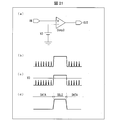
- A is a block diagram which shows the structure of the active optical cable which concerns on a prior art.
- B is a waveform diagram of a data signal input to the connector of the active optical cable.
- (C) is a waveform diagram of an optical signal output from the connector.
- FIG. 6 is a circuit diagram showing a first modification of the IDLE detection circuit shown in FIG. 5.
- FIG. 5 is a circuit diagram showing a first modification of the IDLE detection circuit shown in FIG. 5.
- FIG. 6 is a circuit diagram showing a second modification of the IDLE detection circuit shown in FIG. 5. It is a wave form diagram of the voltage signal in each part of the IDLE detection circuit of FIG.
- FIG. 6 is a circuit diagram showing a third modification of the IDLE detection circuit shown in FIG. 5.
- FIG. 19A is a circuit diagram of an IDLE detection circuit shown in FIG. 5 and a comparator that can be used in place of the low-pass filter included in the IDLE detection circuit shown in FIG. (B) to (d) are waveform diagrams of voltage signals in respective parts of the comparator.
- An active optical cable 1 including an optical transmitter according to an embodiment of the present invention will be described with reference to FIG.
- FIG. 1A is a block diagram showing the configuration of the active optical cable 1.
- the active optical cable 1 includes a cable 4 and a pair of connectors 2 and 3 provided at both ends of the cable 4.
- An optical fiber 11 is accommodated in the cable 4.
- the connector 2 includes an AC coupling capacitor 5, a transmission circuit 6, and an LD (Laser Diode) 7, and functions as an optical transmitter that converts a data signal (voltage signal) into an optical signal and transmits the optical signal.
- the transmission circuit 6 converts a data signal input from the outside (for example, a host device) via the AC coupling capacitor 5 into a current signal. This current signal is supplied to the LD 7.
- the LD 7 converts the current signal supplied from the transmission circuit 6 into an optical signal. This optical signal is transmitted to the connector 3 through the optical fiber 11.
- the transmission circuit 6 is realized as an integrated circuit. Therefore, in FIG. 1A, the transmission circuit 6 is represented as “TX-IC”. However, the transmission circuit 6 is not limited to this, and may be realized as a discrete circuit.
- the AC coupling capacitor 5 may be omitted, and the LD 7 may be replaced with a light emitting element other than the LD, such as a light emitting diode.
- the connector 3 includes a PD (Photo (Diode) 8, a receiving circuit 9, and an AC coupling capacitor 10, and functions as an optical receiver that converts an optical signal into a data signal and outputs the data signal.
- the PD 8 converts the optical signal transmitted from the connector 2 into a current signal. This current signal is supplied to the receiving circuit 9.
- the receiving circuit 9 converts the current signal supplied from the PD 8 into a data signal (voltage signal). This data signal is output to the outside (for example, a host device) via the AC coupling capacitor 10.
- the receiving circuit 9 is realized as an integrated circuit. Therefore, in FIG. 1A, the receiving circuit 9 is represented as “RX-IC”. However, the receiving circuit 9 is not limited to this, and may be realized as a discrete circuit. Further, the AC coupling capacitor 10 may be omitted, and the PD 8 may be replaced with a light receiving element other than the PD such as a phototransistor.
- FIG. 1 is a waveform diagram of a data signal input to the connector 2.
- the data signal input to the connector 2 has a DATA interval in which the value alternately takes a high level and a low level, and an intermediate level between the high level and the low level.
- It is a ternary voltage signal including an IDLE section that continues to be taken.
- the transmission circuit 6 built in the connector 2 includes an IDLE detection circuit 61 (see FIG. 2) for detecting the IDLE section of the data signal, and operates as follows. That is, (1) outside the IDLE section (in the DATA section), the value of the current signal supplied to the LD 7 (the magnitude of the drive current) is controlled to the same logical value as the value of the data signal, and (2) within the IDLE section. The value of the current signal supplied to the LD 7 is controlled to be equal to or less than the threshold current (oscillation start current) of the LD 7 (in this embodiment, 0 [A]).
- FIG. 1 (c) is a waveform diagram of an optical signal output from the connector 2.
- FIG. 1 (c) the optical signal output from the connector 2 alternately takes a high level and a low level outside the IDLE section (in the DATA section), and within the IDLE section, Take off level.
- the off level is a level that is different from the high level and the low level and hardly fluctuates due to external factors.
- the connector 3 can correctly specify the IDLE section of the data signal input to the connector 2 by specifying the period during which the value of the received optical signal is off level.
- the active optical cable 1 may further include a configuration for transmitting an optical signal from the connector 3 side to the connector 2 side in addition to a configuration for transmitting an optical signal from the connector 2 side to the connector 3 side.
- a configuration for transmitting an optical signal from the connector 3 side to the connector 2 side in addition to a configuration for transmitting an optical signal from the connector 2 side to the connector 3 side.
- an AC coupling capacitor 5 ′, a transmission circuit 6 ′, and an LD 7 ′ (not shown) are built in the connector 3
- a PD 8 ′, a reception circuit 9 ′, and an AC coupling capacitor 10 ′ Is built in the connector 2, and (3) the LD 7 'and the PD 8' are connected by an optical fiber 11 '(not shown). Thereby, bidirectional communication becomes possible.
- FIG. 2 is a block diagram illustrating a configuration example of the transmission circuit 6.
- 3A to 3C are waveform diagrams of voltage signals in the respective parts of the transmission circuit 6.
- FIG. 4A to 4F are waveform diagrams of current signals in the respective parts of the transmission circuit 6.
- the transmission circuit 6 includes an IDLE detection circuit 61, a squelch circuit 62, a modulation driver 63, an auxiliary driver 64, a bias current source 65, and a compensation current source 66.
- the IDLE detection circuit 61 detects a section (time zone) in which the value of the data signal is included in a predetermined range between the high level and the low level as an IDLE section. More specifically, a first comparator that identifies a first interval in which the value of the data signal is greater than or equal to the lower limit value of the range, and a second interval in which the value of the data signal is less than or equal to the upper limit value of the range. A second comparator to be identified, and a common portion between the first section and the second section is detected as an IDLE section. The IDLE detection circuit 61 generates an IDLE detection signal indicating an IDLE section.
- the IDLE detection signal generated by the IDLE detection circuit 61 is a voltage signal whose value is at a high level within the IDLE section and whose value is at a low level outside the IDLE section (within the DATA section).
- the waveform of the data signal time change in potential at point Q
- the waveform of the IDLE detection signal time change in potential at point R
- the IDLE detection signal generated by the IDLE detection circuit 61 is input to the squelch circuit 62 and the auxiliary driver 64.
- a configuration example of the IDLE detection circuit 61 will be described later with reference to another drawing.
- the data signal is input to the transmission circuit 6 through the AC coupling capacitor 5. This is why the intermediate level of the data signal shown in FIG. 3A matches the power supply voltage VDD of the transmission circuit 6.
- the squelch circuit 62 identifies the IDLE section with reference to the IDLE detection signal. Further, the squelch circuit 62 corrects the value of the data signal to a low level in the IDLE section. That is, the squelch circuit 62 outputs the low level as the value of the corrected data signal within the IDLE interval, regardless of the value of the data signal before correction, and before the correction, outside the IDLE interval (in the data interval). The data signal value is output as the corrected data signal value.
- the waveform of the data signal before correction is as shown in FIG. 3A and the waveform of the IDLE detection signal is as shown in FIG. 3B
- the waveform of the data signal after correction (the potential at point S) is corrected. (Time change) is as shown in FIG.
- the data signal corrected by the squelch circuit 62 is input to the modulation driver 63.
- the data signal corrected by the squelch circuit 62 is hereinafter referred to as “corrected data signal”.
- the modulation driver 63 modulates the bias current C supplied from the bias current source 65 with the corrected data signal by drawing the modulation current A having a magnitude corresponding to the value of the corrected data signal from the bias current source 65. More specifically, (1) if the value of the corrected data signal is low level, a modulation current A having a predetermined magnitude (IM [A]) is drawn from the bias current source 65, and (2) correction is performed. If the value of the subsequent data signal is high, the modulation current A is stopped. When the waveform of the corrected data signal is as shown in FIG. 3C, the time change in the magnitude of the modulation current A is as shown in FIG. A configuration example of the modulation driver 63 will be described later with reference to another drawing.
- the auxiliary driver 64 identifies the IDLE section with reference to the IDLE detection signal.
- the auxiliary driver 64 draws the auxiliary current B having a predetermined magnitude (IS [A]) from the bias current source 65 in the IDLE section.
- IB is the magnitude of the modulation current A drawn by the modulation driver 63 in the IDLE section
- IB is the magnitude of the bias current C output from the bias current source 65
- (3 ) ⁇ is a positive constant.
- the temporal change in the magnitude of the auxiliary current B is as shown in FIG. 4B. Therefore, the time change in the magnitude of the combined current A + B obtained by combining the modulation current A and the auxiliary current B is as shown in FIG. A configuration example of the auxiliary driver 64 will be described later with reference to another drawing.
- the bias current source 65 outputs a bias current C having a predetermined magnitude (IB [A]).
- the time change of the magnitude of the bias current C is as shown in FIG.
- a part of the bias current C output from the bias current source 65 is drawn into the modulation driver 63 and the auxiliary driver 64 as the modulation current A and the auxiliary current B.
- the remaining part of the bias current C output from the bias current source 65 is supplied as drive current E to the LD 7 via the output terminal OUT. That is, the drive current E obtained by subtracting the auxiliary current B from the difference between the bias current C and the modulation current A is supplied to the LD 7.
- the bias current source 65 can be configured by a DC current source having one end connected to the power supply (voltage VDD) and the other end connected to the output terminal OUT as shown in FIG. 2, for example. Another configuration example of the bias current source 65 will be described later with reference to another drawing.
- the compensation current source 66 compensates for the shortage of the bias current C when the magnitude of the combined current A + B (the modulation current A is IM [A] in the IDLE section) exceeds the bias current C. D is supplied to the auxiliary driver 64.
- the compensation current source 66 When the compensation current source 66 does not exist, the bias current C is insufficient (IM + IS> IB) in the IDLE section, so that the bias current source 65 tries to output a current having a predetermined magnitude IB [A] or more. To do. As a result, a voltage drop at the output terminal OUT occurs, and as a result, the operation of the modulation driver 63 and the auxiliary driver 64 may be hindered.
- the compensation current source 66 can be configured by a diode (diode clamp) having an anode terminal connected to a clamp power supply (voltage Vcramp) and a cathode terminal connected to an output terminal OUT.
- a diode diode clamp
- Vcramp clamp power supply
- cathode terminal connected to an output terminal OUT.
- the LD 7 is quickly turned off at the start point of the IDLE section of the data signal input to the connector 2, and the LD 7 is quickly turned on at the end point of the IDLE section of the data signal input to the connector 2.
- the delay time from the start point / end point of the IDLE section to the turn-off / light-on of the LD 7 is shorter than that in the case where the LD 7 is turned off / light-up by the interruption / break-off of the bias current.
- the magnitude of the drive current E flowing into the LD 7 in the IDLE section can be set to 0 [A]. That is, the LD 7 can be turned off in the IDLE section.
- the auxiliary driver 64 is used to control the drive current E flowing into the LD 7 to 0 [A] in the IDLE section. For this reason, the delay time from the start point / end point of the IDLE section to the turn-off / turn-on of the LD 7 is compared with the case where the turn-off / turn-on of the power supply to the modulation driver 63 and the bias current source 65 is stopped / restarted. Can be shortened.
- the delay time from the start point / end point of the IDLE section to the turn-off / lighting of the LD 7 is 5 n seconds or less. This is 1/6 or less of the delay time (30 nsec or more) when the LD 7 is turned off / on by stopping / resuming the power supply to the modulation driver 63 and the bias current source 65.
- the magnitude of the current flowing out from the LD 7 in the IDLE section may be controlled to be equal to or less than the threshold current (oscillation start current) of the LD 7 and does not need to be controlled to 0 [A]. Even in this case, the LD 7 can be turned off in the IDLE section (including a mode in which the light emission state is set to be low).
- the magnitude IS of the auxiliary current B is set to satisfy IM + IS> IB, but the present invention is not limited to this.
- the drive current E supplied to the LD 7 in the IDLE section is 0 [A]. Further, in this case, since the bias current C is not insufficient in the IDLE section, the compensation current source 66 can be omitted.
- the current signal ⁇ Ib output from the compensator is a differential current signal for canceling the dullness of the rising / falling edge of the current signal ⁇ Ia output from the current driver, and the value of the sum signal ⁇ Ia + ⁇ Ib is specified. It is not for making it zero over a section (for example, an IDLE section).
- the current signal ⁇ I1 output from the error amplifier is a current signal representing the difference between the monitor signal Im and the light emission command signal Isig, and is not for setting the value of the sum signal ⁇ I1 + ⁇ I2 to 0 over a specific section. Absent. Therefore, the semiconductor laser control device described in Patent Document 4 includes the auxiliary driver 64 (provided that the auxiliary current B is drawn from the bias current source 65 to be included in the transmission circuit 6 according to the present embodiment so that the value of the drive current E falls within the IDLE section. It is not provided with a configuration corresponding to 0).
- the IDLE detection circuit 61 can also be realized by a peak hold circuit like the signal detection circuit described in Patent Document 5, for example.
- the reference voltage in the comparator described in Patent Document 5 may be set to a value larger than the intermediate level of the data signal and smaller than the high level of the data signal.
- the response speed of the IDLE detection circuit 61 decreases, and it becomes difficult to achieve the response speed required by standards such as SAS 2.0 and PCIe 3.0.
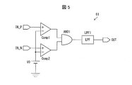
- FIG. 5 is a circuit diagram showing a configuration example of the IDLE detection circuit 61.
- FIG. 6 is a waveform diagram of a voltage signal in each part of the IDLE detection circuit 61 shown in FIG.
- the IDLE detection circuit 61 has a function of detecting a section in which the value of the data signal is included in a predetermined range between the high level and the low level.
- the IDLE detection circuit 61 shown in FIG. 5 implements such a function by the first comparator Comp1, the second comparator Comp2, the AND gate AND1, and the low-pass filter LPF1.
- the data signal is input in the positive phase to the non-inverting input terminal of the first comparator Comp1, and the reference voltage V0 is input to the inverting input terminal of the first comparator Comp1.
- the first comparator Comp1 compares the value of the positive phase data signal with the reference voltage V0, and generates a voltage signal indicating the comparison result.
- the reference voltage V0 is set to the lower limit value of the above range.
- the waveform of the positive phase data signal is as shown in FIG. 6A, and the waveform of the voltage signal generated by the first comparator Comp1 is as shown in FIG. 6B.
- the voltage signal generated by the first comparator Comp1 is input to the AND gate AND1.
- the data signal is input in reverse phase to the non-inverting input terminal of the second comparator Comp2, and the reference voltage V0 is input to the inverting input terminal of the second comparator Comp2.
- the second comparator Comp2 compares the value of the data signal having the opposite phase with the reference voltage V0, and generates a voltage signal indicating the comparison result.
- the waveform of the negative phase data signal is as shown in FIG. 6C, and the waveform of the voltage signal generated by the second comparator Comp2 is as shown in FIG.
- the voltage signal generated by the second comparator Comp2 is input to the AND gate AND1.
- the AND gate AND1 refers to the voltage signal generated by the first comparator Comp1 and the voltage signal generated by the second comparator Comp2, and compares the comparison result of the first comparator Comp1 and the second comparator Comp2. A voltage signal indicating a logical product with the comparison result is generated.
- the waveform of the voltage signal generated by the AND gate AND1 is as shown in FIG.
- the voltage signal generated by the AND gate AND1 is input to the low pass filter LPF1.
- the low-pass filter LPF1 smoothes the voltage signal generated by the AND gate AND1. That is, noise at the time of logic switching included in the voltage signal generated by the AND gate AND1 is removed.
- the waveform of the voltage signal smoothed by the low-pass filter LPF1 is as shown in FIG. That is, the voltage signal smoothed by the low-pass filter LPF1 is a voltage signal whose value is high level within the IDLE section (outside the DATA section) and whose value is low level outside the IDLE section.
- the voltage signal smoothed by the low-pass filter LPF1 is output to the outside (squelch circuit 62 and auxiliary driver 64) as an IDLE detection signal.
- the squelch circuit 62 and the auxiliary driver 64 may be configured to operate with reference to an IDLE detection signal that is at a high level within the IDLE interval, or with reference to an IDLE detection signal that is at a high level outside the IDLE interval. It can also be configured to operate.
- the squelch circuit 62 and the auxiliary driver 64 are configured to operate with reference to the latter IDLE detection signal, for example, the following configuration may be employed. That is, a configuration may be adopted in which the IDLE detection signal output from the IDLE detection circuit 61 is input to the squelch circuit 62 and the auxiliary driver 64 via an inverting amplifier.
- latter stage of AND gate AND1 is employ
- the structure of the IDLE detection circuit 61 is not limited to this. That is, when the operating frequency of the AND gate AND1 is slow and spike noise at the time of logic switching is not included in the voltage signal generated by the AND gate AND1, the AND gate AND1 may be omitted (the first gate described later). (Refer to the modified example).
- a configuration in which each of the positive-phase data signal and the negative-phase data signal is compared with a single reference voltage V0 is employed, but the configuration of the IDLE detection circuit 61 is not limited to this.
- FIG. 7 is a circuit diagram showing a first configuration example of the modulation driver 63 and the auxiliary driver 64.
- the modulation driver 63 can be composed of a pair of transistors (npn transistors) Tr1 and Tr2 and a direct current source DC1.
- the transistor Tr1 has a collector terminal connected to the output point OUT, a base terminal connected to the input point IN1_N, and an emitter terminal connected to the emitter terminal of the transistor Tr2.
- the transistor Tr2 has a collector terminal connected to the power supply (power supply voltage VDD), a base terminal connected to the input point IN1_P, and an emitter terminal connected to the emitter terminal of the transistor Tr1.
- An intermediate point between the emitter terminal of the transistor Tr1 and the emitter terminal of the transistor Tr2 is grounded via the direct current source DC1.
- the current value of the direct current source DC1 can be set from the outside.
- the data signal is input in the positive phase to the input point IN1_P of the modulation driver 63, and the data signal is input in the reverse phase to the input point IN1_N of the modulation driver 63. If the value of the data signal is low level, the modulation driver 63 draws the modulation current A having a predetermined magnitude (IM [A]) from the output point OUT, and (2) the value of the data signal is high level. If there is, the drawing of the modulation current A from the output point OUT is suspended.
- IM [A] a predetermined magnitude
- the auxiliary driver 64 can be composed of a pair of transistors (npn transistors) Tr3 and Tr4 and a direct current source DC2. Since the configuration of the auxiliary driver 64 is the same as that of the modulation driver 63, the description thereof is omitted here.
- the IDLE detection signal is input in reverse phase to the input point IN2_P of the auxiliary driver 64, and the IDLE detection signal is input in positive phase to the input point IN2_N of the auxiliary driver 64.
- the auxiliary driver 64 draws the auxiliary current B having a predetermined magnitude (IS [A]) from the output point OUT, and (2) IDLE. If the value of the detection signal is low level, the modulation current A from the output point OUT is stopped.
- npn transistors are used as the transistors T1 to Tr4 constituting the modulation driver 63 and the auxiliary driver 64, but the present invention is not limited to this. That is, NMOS transistors may be used as the transistors T1 to Tr4 constituting the modulation driver 63 and the auxiliary driver 64.
- FIG. 8 is a circuit diagram showing a second configuration example of the modulation driver 63 and the auxiliary driver 64.
- the modulation driver 63 shown in FIG. 8 has a modulation driver 63 shown in FIG. 7 as a main driver, and a pre-driver that amplifies a data signal is added to the preceding stage.
- the main driver converts the data signal amplified by the pre-driver into a current signal.
- the differential amplifier circuit is a circuit for differentially amplifying data signals, and includes a pair of resistors R1 and R2, a pair of transistors (npn transistors) Tr9 and Tr10, and a direct current source DC7.
- the transistor Tr9 has a collector terminal connected to the power supply (voltage VDD) via the resistor R1, a base terminal connected to the input point IN1_N, and an emitter terminal connected to the emitter terminal of the transistor Tr10.
- the transistor Tr10 has a collector terminal connected to the power supply (voltage VDD) via the resistor R2, a base terminal connected to the input point IN1_P, and an emitter terminal connected to the emitter terminal of the transistor Tr9.
- An intermediate point between the emitter terminal of the transistor Tr9 and the emitter terminal of the transistor Tr10 is grounded via a direct current source DC7.
- the emitter follower circuit is a circuit for making the output impedance of the pre-driver lower than the input impedance of the main driver, and includes a pair of transistors (npn transistors) Tr5 and Tr6 and a pair of direct current sources DC3 and DC4. It is configured.
- the transistor Tr5 has a collector terminal connected to the power supply (voltage VDD), a base terminal connected to one output point of the differential amplifier circuit (collector terminal of the transistor Tr9), and an emitter terminal grounded via the DC current source DC3.
- the emitter voltage of the transistor Tr5 is input to the base terminal of the transistor Tr2 constituting the main driver as a positive-phase data signal.
- the transistor Tr6 has a collector terminal connected to the power supply (voltage VDD), a base terminal connected to the other output point of the differential amplifier circuit (collector terminal of the transistor Tr10), and an emitter terminal connected via the direct current source DC4. Is grounded.
- the emitter voltage of the transistor Tr6 is input to the base terminal of the transistor Tr1 constituting the main driver as a data signal of opposite phase.
- the auxiliary driver 64 shown in FIG. 8 has the auxiliary driver 64 shown in FIG. 7 as a main driver, and a pre-driver that amplifies the IDLE detection signal is added to the preceding stage.
- the main driver converts the IDLE detection signal amplified by the pre-driver into a current signal. Since the configuration of the predriver added to the auxiliary driver 64 is the same as the configuration of the predriver added to the modulation driver 63, the description thereof is omitted here.
- npn transistors are used as the transistors T1 to Tr12 constituting the modulation driver 63 and the auxiliary driver 64, but the present invention is not limited to this. That is, NMOS transistors may be used as T1 to Tr12 constituting the modulation driver 63 and the auxiliary driver 64.
- FIG. 9 is a circuit diagram showing a third configuration example of the modulation driver 63 and the auxiliary driver 64.
- the modulation driver 63 shown in FIG. 9 is obtained by adding a stabilization circuit X1 for stabilizing the output voltage of the pre-driver to the modulation driver 63 shown in FIG.
- the stabilization circuit X1 includes a transistor (PMOS transistor) M1 and a voltage drop amount control circuit that controls the voltage drop amount in the transistor M1 according to the output voltage of the pre-driver.
- the source terminal of the transistor M1 is connected to the power supply (voltage VDD), and the drain terminal of the transistor M1 is connected to the collector terminals of the transistors Tr9 and Tr10 that constitute the differential amplifier circuit of the predriver via resistors R1 and R2. ing.
- the transistor M1 functions as a voltage drop device with a variable voltage drop amount.
- the voltage drop amount control circuit includes a pair of resistors R1 and R2 having the same resistance value and an operational amplifier OP1.
- the resistors R1 and R2 are connected in series between the emitter terminals of the transistors Tr5 and Tr6 constituting the emitter follower circuit of the pre-driver. Further, the voltage at the intermediate point between the resistors R1 and R2 matches the average value of the emitter voltages of the transistors Tr5 and Tr6 (hereinafter referred to as “average emitter voltage”).
- the non-inverting input terminal of the operational amplifier OP1 is connected to the intermediate point between the resistors R1 and R2.
- the average emitter voltage of the transistors Tr5 and Tr6 is input to the non-inverting input terminal of the operational amplifier OP1.
- a predetermined reference voltage V1 is input to the inverting input terminal of the operational amplifier OP1.
- the output terminal of the operational amplifier OP1 is connected to the gate terminal of the transistor M1.
- the stabilization circuit X1 When the output voltage of the pre-driver, that is, the average emitter voltage of the transistors Tr5 and Tr6 exceeds the reference voltage V1, the stabilization circuit X1 operates as follows. That is, the output voltage of the operational amplifier OP1 increases, and as a result, the gate voltage of the transistor M1 increases. As a result, the source-drain resistance of the transistor M1 increases, and as a result, the amount of voltage drop in the transistor M1 increases. As a result, the voltage applied to the pre-driver is reduced, and as a result, the output voltage of the pre-driver is lowered. This operation continues until the average emitter voltage of the transistors Tr5 and Tr6 matches the reference voltage V1.
- the stabilization circuit X1 operates as follows. That is, the output voltage of the operational amplifier OP1 decreases, and as a result, the gate voltage of the transistor M1 increases. As a result, the resistance between the source and drain of the transistor M1 is reduced, and as a result, the amount of voltage drop in the transistor M1 is reduced. As a result, the voltage applied to the pre-driver increases, and as a result, the output voltage of the pre-driver increases. This operation continues until the average emitter voltage of the transistors Tr5 and Tr6 matches the reference voltage V1.
- the output voltage of the predriver varies according to the fluctuation of the power supply voltage of the predriver, in order to prevent the operating conditions of each element constituting the main driver from breaking, strict conditions are imposed on the fluctuation range of the power supply voltage of the predriver. It is necessary to impose. If the stabilization circuit X1 is added, the output voltage of the predriver does not fluctuate according to the fluctuation of the power supply voltage of the predriver, so that it is not necessary to impose strict conditions on the fluctuation range of the power supply voltage of the predriver.
- the auxiliary driver 64 shown in FIG. 9 is obtained by adding a pre-driver stabilization circuit X2 for stabilizing the output voltage of the pre-driver to the auxiliary driver 64 shown in FIG. Since the configuration of the stabilization circuit X2 added to the auxiliary driver 64 is the same as the configuration of the stabilization circuit X1 added to the modulation driver 63, the description thereof is omitted here.
- PMOS transistors are used as the transistors M1 and M2 constituting the stabilization circuits X1 and X2, but the present invention is not limited to this.
- pnp transistors may be used as the transistors constituting the stabilization circuits X1 and X2.
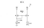
- FIG. 10 is a circuit diagram showing a first configuration example of the bias current source 65.
- the bias current source 65 can be composed of a pair of transistors (PMOS transistors) M3 and M4 and a DC current source DC9.
- the source terminal of the transistor M3 is connected to the power supply (voltage VDD).
- the source terminal of the transistor M4 is connected to the power supply (voltage VDD), and the drain terminal of the transistor M4 is connected to the gate terminal of the transistor M4 and to the gate terminal of the transistor M3. That is, the transistors M3 and M4 form a current mirror circuit having the drain terminal of the transistor M4 as an input point and the drain terminal of the transistor M3 as an output point.
- the sizes of the transistors M3 and M4 are set so that the magnitude of the current C flowing out from the output point of the current mirror circuit is N times the magnitude of the current C ′ flowing out from the input point of the current mirror circuit. ing. Therefore, if a DC current source DC9 that passes the current C ′ of IB / N [A] is connected to the input point of the current mirror circuit, the current C of IB [A] can be extracted from the output point of the current mirror circuit. it can.
- PMOS transistors are used as the transistors M3 and M4 constituting the bias current source 65, but the present invention is not limited to this. That is, pnp transistors may be used as the transistors M3 and M4 constituting the bias current source 65. However, the types of the transistors M3 and M4 are matched. That is, when a PMOS transistor is used as the transistor M3, a PMOS transistor is used as the transistor M4. When a pnp transistor is used as the transistor M3, a pnp transistor is used as the transistor M4.
- FIG. 11 is a circuit diagram showing a second configuration example of the bias current source 65.
- the bias current source 65 can be composed of an operational amplifier OP3, a transistor (PMOS transistor) M5, a pair of resistors R5 and R6, and a direct current source DC10.
- the non-inverting input terminal of the operational amplifier OP3 is connected to the power supply (voltage VDD) via the resistor R6.
- the inverting input terminal of the operational amplifier OP3 is connected to the power supply (voltage VDD) via R5 and to the source terminal of the transistor M5.
- the output terminal of the operational amplifier OP3 is connected to the gate terminal of the transistor M5. That is, the operational amplifier OP3, the transistor M5, and the resistors R5 and R6 constitute a current mirror circuit having the non-inverting input terminal of the operational amplifier OP3 as an input point and the drain terminal of the transistor M5 as an output point.
- a PMOS transistor is used as the transistor M5 constituting the bias current source 65, but the present invention is not limited to this. That is, a pnp transistor may be used as the transistor M5 constituting the bias current source 65.
- the transmission circuit 6 may include (1) only the bias current source 65 configured as shown in FIG. 10, or (2) only the bias current source 65 configured as shown in FIG. (3) Both the bias current source 65 configured as shown in FIG. 10 and the bias current source 65 configured as shown in FIG. 11 are provided, and which bias current source 65 is used. It may be configured to be switchable.
- the use of a bias current source 65 configured as shown in FIG. 10 is suitable for transmission of intermittent signals such as OOB signals defined in SAS 2.0.
- the bias current source 65 configured as shown in FIG. 10 has a tendency that the current ratio tends to fluctuate with respect to the fluctuation of the power supply (voltage VDD), but is resistant to abrupt fluctuation of the bias voltage of the LD 7 and from the IDLE section.
- the use of the bias current source 65 configured as shown in FIG. 11 is suitable for transmission of a continuous signal defined in the InfiniBand standard or the like.
- the bias current source 65 configured as shown in FIG. 11 has a tendency that the current ratio is less likely to fluctuate with respect to the fluctuation of the power supply (voltage VDD), but is weak against the abrupt fluctuation of the bias voltage of the LD7, and the This is because the response time to the transition to the section is long. Therefore, by adopting a configuration in which the bias current source to be used is switched to the one suitable for the type of data signal to be transmitted, the transmission circuit 6 suitable for both intermittent signal transmission and continuous signal transmission can be realized.
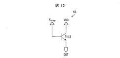
- FIG. 12 is a circuit diagram showing a first configuration example of the compensation current source 66.
- the compensation current source 66 can be configured by a transistor (npn transistor) Tr13.
- the collector terminal of the transistor Tr13 is connected to a power supply (voltage VDD), and the base terminal of the transistor Tr13 is connected to a clamp power supply (voltage Vcramp).
- a Pnpn transistor is used as the transistor Tr13 constituting the compensation current source 66, but the present invention is not limited to this. That is, an NMOS transistor may be used as the transistor Tr13 constituting the compensation current source 66.
- FIG. 13 is a circuit diagram showing a second configuration of the compensation current source 66.
- a compensation current source 66 shown in FIG. 13 is obtained by adding an operational amplifier OP4 to the compensation current source 66 shown in FIG.
- a non-inverting input terminal and an output terminal are directly connected so as to constitute a voltage follower circuit.
- the inverting input terminal of the operational amplifier OP4 is connected to the clamp power supply (voltage Vcramp), and the output terminal of the operational amplifier OP4 is connected to the base terminal of the transistor Tr13.
- the transmission circuit 6 and the LD 7 shown in FIG. 2 can be replaced with the transmission circuit 16 and the LD 17 shown in FIG.
- the LD 7 shown in FIG. 2 is an LD such as a VCSEL (Vertical Cavity Emitting Laser) that can control the amount of light emission by changing the magnitude of the driving current that flows.
- Reference numeral 6 denotes a transmission circuit suitable for such an LD.
- the transmission circuit 6 shown in the figure is not limited to the LD, and any light emitting element can be used as long as the light emission amount can be controlled by changing the magnitude of the inflowing drive current. It can be used as a light source.
- the transmission circuit 16 shown in the figure is a transmission circuit suitable for such an LD.
- the transmission circuit 16 shown in the figure is not limited to the LD, and any light emitting element can be used as long as the light emission amount can be controlled by changing the magnitude of the inflowing drive current. It can be used as a light source.
- FIG. 14 is a block diagram showing a configuration of the transmission circuit 16 according to this modification.
- the transmission circuit 16 includes an IDLE detection circuit 161, a squelch circuit 162, a modulation driver 163, an auxiliary driver 164, a bias current source 165, and a compensation current source 166. I have.
- the functions of the IDLE detection circuit 161 and the squelch circuit 162 included in the transmission circuit 16 according to this modification are the same as the functions of the IDLE detection circuit 61 and the squelch circuit 62 included in the transmission circuit 6 illustrated in FIG. The description is omitted here.
- the function of each of the modulation driver 163, the auxiliary driver 164, the bias current source 165, and the compensation current source 166 included in the transmission circuit 16 according to this modification will be described.
- the modulation driver 163 sucks the modulation current A having a magnitude corresponding to the value of the corrected data signal obtained by the squelch circuit 162. More specifically, (1) if the value of the corrected data signal is high, the modulation current A having a predetermined magnitude (IM [A]) is sucked, and (2) the value of the corrected data signal If is low level, the absorption of the modulation current A is stopped.
- the auxiliary driver 164 specifies the IDLE section with reference to the IDLE detection signal obtained by the IDLE detection circuit 161. Further, the auxiliary driver 164 discharges the auxiliary current B having a predetermined magnitude (IS [A]) in the IDLE section.
- the bias current source 165 sucks a bias current C having a predetermined magnitude (IB [A]).
- the bias current source 165 can be configured by a DC current source having one end connected to the output terminal OUT and the other end grounded, for example, as shown in FIG.
- the compensation current source 166 has a shortage of the bias current C when the difference obtained by subtracting the magnitude of the modulation current A (0 [A] in the IDLE section) from the magnitude of the auxiliary current B exceeds the magnitude of the bias current C.
- the compensation current D is compensated for.
- the compensation current source 166 can be configured by a diode (diode clamp) having an anode terminal connected to the output terminal OUT and a cathode terminal grounded.
- the compensation current source 166 shown in FIG. 14 draws the compensation current D from the output terminal OUT when the anode-cathode voltage of the diode exceeds the threshold voltage Vth, that is, when the voltage at the output terminal OUT exceeds the threshold voltage Vth.
- the modulation driver 163, the auxiliary driver 164, the bias current source 165, the compensation current source 166, and the LD 17 apply the modulation current A to the sum (C + D) of the bias current C and the compensation current D.
- the driving current E (C + D) + AB obtained by subtracting the auxiliary current B is connected so as to flow out of the LD 17.
- the magnitude of the drive current E flowing out from the LD 17 in the IDLE section can be set to 0 [A]. That is, the LD 17 can be turned off in the IDLE section.
- the auxiliary driver 164 is used to control the magnitude of the drive current E flowing out of the LD 17 in the IDLE section to 0 [A]. For this reason, the delay time from the start point / end point of the IDLE section to the turn-off / light-on of the LD 17 can be shortened as compared with the case where the LD 17 is turned off / light-up by blocking / unblocking the bias current.
- this invention is not limited to this. That is, a configuration may be employed in which the magnitude of the drive current E flowing out from the LD 17 in the IDLE section is made equal to or less than the threshold current (oscillation start current) of the LD 17. Even in this case, the LD 17 can be turned off (including a mode in which the light emission state is set) in the IDLE section.
- the LD 17 can be reliably turned off in the IDLE section. This is because the magnitude IS of the auxiliary current B discharged by the auxiliary driver 164 in the IDLE section is set so as to satisfy IS> IB. Moreover, according to the transmission circuit 16 according to the present modification, even if the magnitude IS of the auxiliary current B exceeds the magnitude of the bias current C in the IDLE section, a voltage drop occurs at the output terminal OUT, and the modulation driver 163 and the auxiliary There is no concern of hindering the operation of the driver 164. This is because the shortage of the bias current C is compensated by the compensation current D discharged from the compensation current source 166 when the magnitude IS of the auxiliary current B exceeds the magnitude IB of the bias current C.
- a configuration is adopted in which the magnitude IS of the auxiliary current B sucked by the auxiliary driver 164 in the IDLE section is set so as to satisfy IS> IB.
- FIG. 17 is a circuit diagram showing a configuration of an IDLE detection circuit 61a according to this modification.
- the IDLE detection circuit 61a includes a first comparator Comp1, a second comparator Comp2, and an AND gate AND1 as in the IDLE detection circuit 61 shown in FIG.
- the operating frequency of the AND gate AND1 is set sufficiently low (for example, 1/10 or less of the operating frequency of the comparators Comp1 and Comp2) so that the generated voltage signal does not include spike noise at the time of logic switching. ing.
- the low-pass filter LPF1 for removing spike noise at the time of logic switching is omitted.
- the IDLE detection circuit 61 shown in FIG. 5 and the IDLE detection circuit 61a shown in FIG. 17 compare each of the value of the positive phase data signal and the value of the negative phase data signal with a single reference voltage V0.
- a section included in a range where the signal value is not less than the lower limit value V0 and not more than the upper limit value 2 ⁇ Vcom ⁇ V0 is detected as an IDLE section (Vcom represents a common voltage of the data signal).
- Vcom represents a common voltage of the data signal.
- this method has the common advantage that a single reference voltage source can be used at the cost of not being able to set the lower and upper limits of the range independently.
- the IDLE detection circuit 61a shown in FIG. 17 has the further advantage that the circuit configuration can be simplified compared to the IDLE detection circuit 61a shown in FIG. 5 because the low-pass filter LPF1 is omitted.
- FIG. 18 is a circuit diagram showing a configuration of an IDLE detection circuit 61b according to this modification.
- FIG. 19 is a waveform diagram of a voltage signal in each part of the IDLE detection circuit 61b according to this modification.
- the IDLE detection circuit 61b according to the present modification includes a first comparator Comp1, a second comparator Comp2, an AND gate AND1, and a low-pass filter LPF1, similarly to the IDLE detection circuit 61. .
- the IDLE detection circuit 61b according to this modification is different from the IDLE detection circuit 61 in the following two points.
- the first difference is that the data signal is input in the same phase (in the positive phase in this modification) to each of the non-inverting input terminal of the first comparator Comp1 and the inverting input terminal of the second comparator Comp2. is there. That is, a positive-phase data signal having a waveform illustrated in FIG. 19A is input to each of the two comparators Comp1 and Comp2.
- the second difference is that different reference voltages V0a and V0b are input to the inverting input terminal of the first comparator Comp1 and the non-inverting input terminal of the second comparator Comp2.
- the data signal is input in the positive phase to the non-inverting input terminal of the first comparator Comp1, and the reference voltage V0a is input to the inverting input terminal of the first comparator Comp1.
- the first comparator Comp1 compares the value of the positive-phase data signal with the reference voltage V0a and generates a voltage signal indicating the comparison result.
- the reference voltage V0a is set to a lower limit value of a predetermined range between the high level and the low level of the data signal.
- the waveform of the positive phase data signal is as shown in FIG. 19B, and the waveform of the voltage signal generated by the first comparator Comp1 is as shown in FIG. 19C.
- the voltage signal generated by the first comparator Comp1 is input to the AND gate AND1.
- the data signal is input in the positive phase to the inverting input terminal of the second comparator Comp2, and the reference voltage V0b is input to the non-inverting input terminal of the second comparator Comp2.
- the second comparator Comp2 compares the value of the positive-phase data signal with the reference voltage V0b and generates a voltage signal indicating the comparison result.
- the reference voltage V0b is set to the upper limit value of the above range.
- the waveform of the positive phase data signal is as shown in FIG. 19D, and the waveform of the voltage signal generated by the second comparator Comp2 is as shown in FIG.
- the voltage signal generated by the second comparator Comp2 is input to the AND gate AND1.
- the AND gate AND1 refers to the voltage signal generated by the first comparator Comp1 and the voltage signal generated by the second comparator Comp2, and compares the comparison result of the first comparator Comp1 and the second comparator Comp2. A voltage signal indicating a logical product with the comparison result is generated.
- the waveform of the voltage signal generated by the AND gate AND1 is as shown in FIG.
- the voltage signal generated by the AND gate AND1 is input to the low pass filter LPF1.
- the low-pass filter LPF1 smoothes the voltage signal generated by the AND gate AND1. That is, noise at the time of logic switching included in the voltage signal generated by the AND gate AND1 is removed.
- the waveform of the voltage signal smoothed by the low-pass filter LPF1 is as shown in FIG. That is, the voltage signal smoothed by the low-pass filter LPF1 is a voltage signal whose value is high level within the IDLE section (outside the DATA section) and whose value is low level outside the IDLE section.
- the voltage signal smoothed by the low-pass filter LPF1 is output to the outside (squelch circuit 62 and auxiliary driver 64) as an IDLE detection signal.
- a positive phase data signal is input to each of the non-inverting input terminal of the first comparator Comp1 and the inverting input terminal of the second comparator Comp2, but a reverse phase data signal is input. Also good. Even in this case, it is possible to obtain a voltage signal whose value is at a high level within the IDLE interval and whose value is at a low level outside the IDLE interval.
- the squelch circuit 62 and the auxiliary driver 64 may be configured to operate with reference to an IDLE detection signal that is at a high level within the IDLE interval, or with reference to an IDLE detection signal that is at a high level outside the IDLE interval. It can also be configured to operate.
- the squelch circuit 62 and the auxiliary driver 64 are configured to operate with reference to the latter IDLE detection signal, for example, the following configuration may be employed. That is, a configuration may be adopted in which the IDLE detection signal output from the IDLE detection circuit 61b is input to the squelch circuit 62 and the auxiliary driver 64 via an inverting amplifier.
- FIG. 20 is a circuit diagram showing a configuration of an IDLE detection circuit 61c according to this modification.
- the IDLE detection circuit 61c includes a first comparator Comp1, a second comparator Comp2, and an AND gate AND1 like the IDLE detection circuit 61b shown in FIG.
- the operating frequency of the AND gate AND1 is set sufficiently low (for example, 1/10 or less of the operating frequency of the comparators Comp1 and Comp2) so that the generated voltage signal does not include spike noise at the time of logic switching. ing.
- the low-pass filter LPF1 for removing spike noise at the time of logic switching is omitted.
- the IDLE detection circuit 61b shown in FIG. 18 and the IDLE detection circuit 61c shown in FIG. 20 compare the positive-phase data signal with each of the two reference voltages V0a and V0b, so that the value of the data signal is equal to or higher than the lower limit value V0a.
- a section included in a range that is equal to or lower than the upper limit value V0b is detected as an IDLE section.
- the IDLE interval can be reliably detected regardless of the difference between the intermediate level of the data signal and the common voltage of the data signal.
- This method has the advantage that the lower limit value and the upper limit value of the range can be set independently as a price for not being able to use only one reference voltage source.
- the IDLE detection circuit 61c shown in FIG. 20 has the further advantage that the circuit configuration can be simplified compared to the IDLE detection circuit 61b shown in FIG. 18 because the low-pass filter LPF1 is omitted.
- FIG. 21A is a circuit diagram of a comparator Comp3 that can be replaced with the low-pass filter LPF1
- FIGS. 21B to 13D are waveform diagrams of voltage signals in each part of the comparator Comp3.
- the comparator Comp3 smoothes the voltage signal generated by the AND gate AND1 similarly to the low-pass filter LPF1. That is, it has a function of removing noise at the time of logic switching included in the voltage signal generated by the AND gate AND1.
- a voltage signal generated by the AND gate AND1 and having a waveform as shown in FIG. 21B is input to the non-inverting input terminal of the comparator Comp3.
- This voltage signal includes noise at the time of logic switching.
- the reference voltage V3 is input to the inverting input terminal of the third comparator Comp3.
- the comparator Comp3 compares the voltage signal generated by the AND gate AND1 with the reference voltage V3, and generates a voltage signal indicating the comparison result.
- the reference voltage V3 is set to be lower than the output voltage of the AND gate AND1 at the high level and higher than the noise peak voltage at the time of logic switching.
- the voltage signal generated by the comparator Comp3 is as shown in FIG. That is, the output signal of the comparator Comp3 is a voltage signal whose value becomes high level within the IDLE interval (outside the DATA interval) and becomes low level outside the IDLE interval, like the output signal of the low pass filter LPF1.
- the optical transmitter according to the present embodiment is an optical transmitter including a transmission circuit that converts a data signal into a current signal and a light-emitting element that converts the current signal into an optical signal.
- the circuit includes an IDLE detection circuit that detects a period in which a value of the data signal is included in a predetermined range between a high level and a low level as an IDLE section, and the current signal is detected in the IDLE section. Is controlled to be equal to or lower than the threshold current of the light emitting element.
- the optical transmission method is an optical transmission method including a first conversion step of converting a data signal into a current signal and a second conversion step of converting the current signal into an optical signal,
- the first conversion step includes a detection step of detecting a period in which a value of the data signal is included in a predetermined range between a high level and a low level as an IDLE interval, and the current in the IDLE interval.
- a control step of controlling the value of the signal to be equal to or less than the threshold current of the light emitting element.
- the light emitting element in the IDLE section of the data signal input to the transmitter (period in which the value of the data signal input to the transmitter continues to take an intermediate level between high level and low level),
- the light emitting element can be turned off. That is, in the IDLE section of the data signal input to the transmitter, the optical signal value (light intensity) output from the transmitter is set to a high level (the optical signal value when the data signal value is high level). Value) and low level (value of the optical signal when the value of the data signal is low level), and can be set to an off level that does not fluctuate due to external factors. For this reason, the receiver can correctly specify the IDLE section of the data signal input to the optical transmitter by specifying the period during which the value of the optical signal output from the optical transmitter is off level. it can.
- “turning off the light emitting element” includes a mode of “making the light emitting element in a slightly light emitting state”.
- the IDLE detection circuit compares the value of the data signal with the upper limit value of the range, and compares the value of the data signal with the lower limit value of the range.
- a second comparator an AND gate that takes a logical product of the output of the first comparator and the output of the second comparator, and a low-pass filter that smoothes the output of the AND gate. preferable.
- the IDLE area of the data signal input into the said transmitter can be pinpointed correctly, and the IDLE detection signal which has an edge in the start point and end point of the specified IDLE area is produced
- the transmission circuit includes a modulation driver that sucks a modulation current according to the data signal, and an auxiliary driver that sucks or discharges an auxiliary current in the IDLE section, and the light emitting element Is a light emitting element in which a driving current obtained by subtracting the auxiliary current from the difference or sum of the bias current and the modulation current flows in or out, and the magnitude of the auxiliary current is the magnitude of the driving current in the IDLE section. It is preferably set to be equal to or lower than the threshold current of the light emitting element.
- the auxiliary driver sucks the auxiliary current in the IDLE section.
- the magnitude of the auxiliary current is preferably set such that the sum of the magnitude of the modulation current in the IDLE is equal to or greater than the magnitude of the bias current.
- the light emitting element is immediately turned off at the start point of the IDLE section of the data signal input to the transmitter, and the light emission is promptly performed at the end point of the IDLE section of the data signal input to the transmitter.
- the element can be lit.
- the delay time from the start point / end point of the IDLE section to the extinction / lighting-on of the light-emitting element is shorter than the case where the light-emitting element is extinguished / lighted by cutoff / release of the bias current.
- the magnitude of the auxiliary current is set so that the sum of the magnitude of the modulation current in the IDLE section is larger than the magnitude of the bias current.
- the circuit includes a compensation current source that supplies a compensation current to the auxiliary driver that compensates for the shortage of the bias current when the sum of the magnitude of the modulation current and the magnitude of the auxiliary current exceeds the magnitude of the bias current. Furthermore, it is preferable to provide.
- the compensation current source When the compensation current source is not present, the bias current is insufficient in the IDLE section, and thus the operation of the modulation driver and the auxiliary driver may be hindered by a voltage drop at the output terminal of the transmission circuit. .
- the compensation current compensates for this shortage in the IDLE section, so that the voltage drop at the output terminal of the transmission circuit does not hinder the operation of the modulation driver and the auxiliary driver. .
- the modulation driver includes a pre-driver that amplifies the data signal and a main driver that converts the data signal amplified by the pre-driver into the current signal. Is preferred.
- the amplitude of the data signal input to the main driver (the potential difference between the high level and the low level) is set to a predetermined level. It may be necessary to do so.
- the amplitude of the data signal input to the main driver can be set to a predetermined value by the pre-driver. Therefore, the amplitude of the current signal output from the main driver can be set to a predetermined level without distorting the current signal.
- the amplitude (light intensity difference between the high level and the low level) can be set to a predetermined magnitude without distorting the optical signal output from the light emitting element.
- the modulation driver includes a voltage drop inserted between a power source and the pre-driver, and a voltage of the voltage drop according to the magnitude of the output voltage of the pre-driver. It is preferable to further include a control circuit that controls the descending amount.
- the auxiliary driver includes a predriver that amplifies the IDLE detection signal indicating the IDLE section, and a main driver that converts the IDLE detection signal amplified by the predriver into the current signal. It is preferable to comprise.
- the magnitude of the drawn current can be set to a predetermined value.
- the auxiliary driver includes a voltage drop inserted between a power source and the pre-driver, and a voltage of the voltage drop according to the magnitude of the output voltage of the pre-driver. It is preferable to further include a control circuit that controls the descending amount.
- the bias current source that generates the bias current is connected to a first current mirror circuit configured by a pair of transistors and an input point of the first current mirror circuit.
- the optical transmitter includes a first current mirror circuit configured by a pair of transistors, and a first DC current source connected to an input point of the first current mirror circuit.
- the first bias current source is used as the bias current source, and the data signal to be transmitted is a continuous signal.
- the first bias current source is suitable for both continuous signal transmission and intermittent signal transmission such as an OOB signal because it does not hinder the operation even if the voltage at the output point fluctuates.
- the second bias current source is not suitable for transmission of intermittent signals, but the fluctuation of the output bias current can be made smaller than that of the first bias current source. Therefore, according to the above configuration, it is possible to transmit both intermittent signals and continuous signals, and it is possible to further suppress fluctuations in the output bias current when transmitting continuous signals.
- the compensation current source has an anode terminal connected to the clamp power supply and a diode, a base terminal connected to the clamp power supply, or a gate terminal connected to the clamp power supply. It is preferable to include an NMOS transistor.
- the compensation current source can be output with a simple configuration.
- the compensation current source includes a voltage follower circuit connected to a clamp power supply, and an npn transistor whose base terminal is connected to the clamp power supply via the voltage follower circuit, or It is preferable to include an NMOS transistor whose gate terminal is connected to the clamp power source via a voltage follower circuit.
- the compensation current source can be output with a simple configuration.
- the transmission circuit includes a modulation driver that sucks a modulation current according to the data signal, and an auxiliary driver that sucks or discharges an auxiliary current in the IDLE section, and the light emitting element Is a light emitting element in which a driving current obtained by subtracting the auxiliary current from the difference or sum of the bias current and the modulation current flows in or out, and the magnitude of the auxiliary current is the magnitude of the driving current in the IDLE section. It is preferably set to be equal to or lower than the threshold current of the light emitting element.
- the auxiliary driver discharges the auxiliary current in the IDLE section.
- the magnitude of the auxiliary current is preferably set to be equal to or greater than the magnitude of the bias current.
- the light emitting element is immediately turned off at the start point of the IDLE section of the data signal input to the transmitter, and the light emission is promptly performed at the end point of the IDLE section of the data signal input to the transmitter.
- the element can be lit.
- the delay time from the start point / end point of the IDLE section to the extinction / lighting-on of the light-emitting element is shorter than the case where the light-emitting element is extinguished / lighted by cutoff / release of the bias current.
- the magnitude of the auxiliary current is set to be larger than the magnitude of the bias current, and the transmitter circuit determines the modulation current from the magnitude of the auxiliary current. It is preferable to further include a compensation current source for discharging a compensation current that compensates for the shortage of the bias current when the difference obtained by subtracting the magnitude exceeds the magnitude of the bias current.
- the compensation current source When the compensation current source is not present, the bias current is insufficient in the IDLE section, and thus the operation of the modulation driver and the auxiliary driver may be hindered by a voltage drop at the output terminal of the transmission circuit. .
- the compensation current compensates for this shortage in the IDLE section, so that the voltage drop at the output terminal of the transmission circuit does not hinder the operation of the modulation driver and the auxiliary driver. .
- an active optical cable in which the optical transmitter is built in a connector is also included in the category of this embodiment.
- the IDLE detection circuit includes a first comparator that identifies a first section in which the value of the data signal is equal to or higher than the lower limit value of the range, and the value of the data signal is the value of the data signal. It is preferable that a second comparator for specifying a second section that is equal to or lower than the upper limit value of the range is provided, and that a common portion between the first section and the second section is detected as an IDLE section.
- the start point and end point of the IDLE area of the data signal input into the said transmitter can be pinpointed correctly, and the IDLE detection signal which has an edge in the start point and end point of the specified IDLE area can be produced
- the first comparator identifies the first section by comparing the value of the data signal with a reference voltage
- the second comparator includes the data signal. It is preferable that the second section is specified by comparing the value of the negative-phase signal with the reference voltage.
- only one reference voltage source can be used. Note that the above configuration is suitable when the data signal is provided in a differential signal system because the IDLE section of the data signal is specified using the normal phase and reverse phase data signals.
- the first comparator identifies the first interval by comparing the value of the data signal with a first reference voltage
- the second comparator Preferably, the second interval is identified by comparing the value of the data signal with a second reference voltage.
- the lower limit value and the upper limit value of the range can be set independently. Note that the above configuration is suitable for the case where the data signal is provided in a single-ended manner because the IDLE section of the data signal is specified using a normal phase or reverse phase data signal.
- the IDLE detection circuit further includes an AND gate that takes a logical product of the output of the first comparator and the output of the second comparator.
- the IDLE detection signal which has an edge in the start point of the specified IDLE area, and an end point can be produced
- the IDLE detection circuit further includes a low-pass filter that smoothes the output of the AND gate.
- spike noise at the time of logic switching that may be included in the IDLE detection signal generated by the AND data can be removed.
- the IDLE detection circuit further includes a comparator that smoothes the output of the AND gate.
- spike noise at the time of logic switching that may be included in the IDLE detection signal generated by the AND data can be removed.
- the control for reducing the drive current supplied to the light emitting element in the IDLE section to be equal to or lower than the threshold current is realized using the auxiliary driver, but the present invention is not limited to this.
- the present invention is not limited to this.
- the drive current supplied to the light emitting element can be controlled to be equal to or less than the threshold current.
- An optical transmitter that performs such control in the IDLE section is also included in the scope of the present invention.
- the present invention can be suitably used for an optical transmitter that transmits a data signal including an OOB pattern or the like.
- the present invention contributes to the realization of an optical transmitter conforming to a communication standard premised on the use of a metal cable such as SAS 2.0 or PCIe 3.0.
Abstract
Description
本発明の一実施形態に係る光送信器を備えたアクティブ光ケーブル1について、図1を参照して説明する。 [Active optical cable]
An active
上述した送信回路6について、図2~図4を参照して説明する。図2は、送信回路6の構成例を示すブロック図である。図3の(a)~(c)は、送信回路6の各部における電圧信号の波形図である。図4の(a)~(f)は、送信回路6の各部における電流信号の波形図である。 [Transmission circuit]
The
上述したIDLE検出回路61の構成例について、図5~図6を参照して説明する。図5は、IDLE検出回路61の構成例を示す回路図である。図6は、図5に示すIDLE検出回路61の各部における電圧信号の波形図である。 [Configuration example of IDLE detection circuit]
A configuration example of the
上述した変調ドライバ63及び補助ドライバ64の構成例について、図7~図9を参照して説明する。 [Configuration example of modulation driver and auxiliary driver]
Configuration examples of the
上述したバイアス電流源65の構成例について、図10~図11を参照して説明する。 [Configuration example of bias current source]
A configuration example of the bias
上述した補償電流源66の構成例について、図12~図13を参照して説明する。 [Configuration example of compensation current source]
A configuration example of the compensation
本実施形態に係るアクティブ光ケーブル1においては、図2に示す送信回路6及びLD7を、図14に示す送信回路16及びLD17に置き換えることが可能である。 [Modified example of transmission circuit and LD]
In the active
図5に示すIDLE検出回路61の第1の変形例について、図17を参照して説明する。図17は、本変形例に係るIDLE検出回路61aの構成を示す回路図である。 [First Modification of IDLE Detection Circuit]
A first modification of the
図5に示すIDLE検出回路61の第2の変形例について、図18及び図19を参照して説明する。図18は、本変形例に係るIDLE検出回路61bの構成を示す回路図である。図19は、本変形例に係るIDLE検出回路61bの各部における電圧信号の波形図である。 [Second Modification of IDLE Detection Circuit]
A second modification of the
図5に示すIDLE検出回路61の第3の変形例について、図20を参照して説明する。図20は、本変形例に係るIDLE検出回路61cの構成を示す回路図である。 [Third Modification of IDLE Detection Circuit]
A third modification of the
なお、図5に図示したIDLE検出回路61及び図18に図示したIDLE検出回路61bが備えているローパスフィルタLPF1は、コンパレータに置き換えることが可能である。図21の(a)は、ローパスフィルタLPF1と置換可能なコンパレータComp3の回路図であり、(b)~(d)は、コンパレータComp3の各部における電圧信号の波形図である。 [Additional Notes on IDLE Detection Circuit]
The low-pass filter LPF1 provided in the
以上のように、本実施形態に係る光送信器は、データ信号を電流信号に変換する送信回路と上記電流信号を光信号に変換する発光素子とを備えた光送信器であって、上記送信回路は、上記データ信号の値がハイレベルとローレベルとの間の予め定められたレンジに含まれている期間をIDLE区間として検出するIDLE検出回路を備えており、上記IDLE区間において上記電流信号の値を上記発光素子の閾値電流以下に制御する、ことを特徴とする。 [Summary]
As described above, the optical transmitter according to the present embodiment is an optical transmitter including a transmission circuit that converts a data signal into a current signal and a light-emitting element that converts the current signal into an optical signal. The circuit includes an IDLE detection circuit that detects a period in which a value of the data signal is included in a predetermined range between a high level and a low level as an IDLE section, and the current signal is detected in the IDLE section. Is controlled to be equal to or lower than the threshold current of the light emitting element.
本発明は上述した実施形態に限定されるものではなく、請求項に示した範囲で種々の変更が可能である。すなわち、請求項に示した範囲で適宜変更した技術的手段を組み合わせて得られる実施形態についても本発明の技術的範囲に含まれる。 [Additional Notes]
The present invention is not limited to the above-described embodiments, and various modifications can be made within the scope shown in the claims. That is, embodiments obtained by combining technical means appropriately modified within the scope of the claims are also included in the technical scope of the present invention.
2 コネクタ
3 コネクタ
4 ケーブル
5 AC結合用コンデンサ
6 送信回路
7 LD
8 PD
9 受信回路
10 AC結合用コンデンサ
11 光ファイバ
61 IDLE検出回路
62 スケルチ回路
63 変調ドライバ
64 補助ドライバ
65 バイアス電流源
66 補償電流源
A 変調電流
B 補助電流
C バイアス電流
D 補償電流
E 駆動電流 1
8 PD
9 Receiving
Claims (20)
- 3値のデータ信号を電流信号に変換する送信回路と上記電流信号を光信号に変換する発光素子とを備えた光送信器であって、
上記送信回路は、上記データ信号の値がハイレベルとローレベルとの間の予め定められたレンジに含まれている期間をIDLE区間として検出するIDLE検出回路を備えており、上記IDLE区間において上記電流信号の値を上記発光素子の閾値電流以下に制御する、
ことを特徴とする光送信器。 An optical transmitter comprising a transmission circuit that converts a ternary data signal into a current signal and a light emitting element that converts the current signal into an optical signal,
The transmission circuit includes an IDLE detection circuit that detects a period in which a value of the data signal is included in a predetermined range between a high level and a low level as an IDLE section. In the IDLE section, the transmission circuit includes the IDLE detection circuit. Controlling the value of the current signal below the threshold current of the light emitting element;
An optical transmitter characterized by that. - 上記IDLE検出回路は、上記データ信号の値が上記レンジの下限値以上となる第1の区間を特定する第1のコンパレータと、上記データ信号の値が上記レンジの上限値以下となる第2の区間を特定する第2のコンパレータとを備えており、上記第1の区間と上記第2の区間との共通部分をIDLE区間として検出する、
ことを特徴とする請求項1に記載の光送信器。 The IDLE detection circuit includes: a first comparator that identifies a first section in which the value of the data signal is equal to or greater than a lower limit value of the range; A second comparator for specifying a section, and detecting a common part of the first section and the second section as an IDLE section.
The optical transmitter according to claim 1. - 上記第1のコンパレータは、上記データ信号の値を基準電圧と比較することによって、上記第1の区間を特定し、
上記第2のコンパレータは、上記データ信号の逆相信号の値を上記基準電圧と比較することによって、上記第2の区間を特定する、
ことを特徴とする請求項2に記載の光送信器。 The first comparator identifies the first interval by comparing the value of the data signal with a reference voltage,
The second comparator identifies the second interval by comparing the value of the reverse phase signal of the data signal with the reference voltage.
The optical transmitter according to claim 2. - 上記第1のコンパレータは、上記データ信号の値を第1の基準電圧と比較することによって、上記第1の区間を特定し、
上記第2のコンパレータは、上記データ信号の値を第2の基準電圧と比較することによって、上記第2の区間を特定する、
ことを特徴とする請求項2に記載の光送信器。 The first comparator identifies the first interval by comparing the value of the data signal with a first reference voltage;
The second comparator identifies the second interval by comparing the value of the data signal with a second reference voltage;
The optical transmitter according to claim 2. - 上記IDLE検出回路は、上記第1のコンパレータの出力と上記第2のコンパレータの出力との論理積を取るANDゲートを更に備えている、
ことを特徴とする請求項2~4の何れか1項に記載の光送信器。 The IDLE detection circuit further includes an AND gate that calculates a logical product of the output of the first comparator and the output of the second comparator.
The optical transmitter according to any one of claims 2 to 4, wherein: - 上記IDLE検出回路は、上記ANDゲートの出力を平滑化するローパスフィルタを更に備えている、
ことを特徴とする請求項5に記載の光送信器。 The IDLE detection circuit further includes a low-pass filter for smoothing the output of the AND gate.
The optical transmitter according to claim 5. - 上記IDLE検出回路は、上記ANDゲートの出力を平滑化するコンパレータを更に備えている、
ことを特徴とする請求項5に記載の光送信器。 The IDLE detection circuit further includes a comparator for smoothing the output of the AND gate.
The optical transmitter according to claim 5. - 上記送信回路は、上記データ信号に応じた変調電流を吸い込む変調ドライバと、上記IDLE区間において補助電流を吸い込む又は吐き出す補助ドライバとを備えており、
上記発光素子は、バイアス電流と上記変調電流との差又は和から上記補助電流を引いた駆動電流が流入又は流出する発光素子であり、
上記補助電流の大きさは、上記IDLE区間における駆動電流の大きさが上記発光素子の閾値電流以下になるように設定されている、
ことを特徴とする請求項1~7の何れか1項に記載の光送信器。 The transmission circuit includes a modulation driver that sucks a modulation current according to the data signal, and an auxiliary driver that sucks or discharges an auxiliary current in the IDLE section.
The light emitting element is a light emitting element in which a driving current obtained by subtracting the auxiliary current from the difference or sum of the bias current and the modulation current flows in or out,
The magnitude of the auxiliary current is set so that the magnitude of the drive current in the IDLE section is equal to or less than the threshold current of the light emitting element.
The optical transmitter according to any one of claims 1 to 7, characterized in that: - 上記補助ドライバは、上記IDLE区間において上記補助電流を吸い込むものであり、
上記発光素子は、上記バイアス電流と上記変調電流との差から上記補助電流を引いた上記駆動電流が流入する発光素子であり、
上記補助電流の大きさは、上記IDLEにおける上記変調電流の大きさとの和が上記バイアス電流の大きさ以上になるように設定されている、
ことを特徴とする請求項8に記載の光送信器。 The auxiliary driver sucks the auxiliary current in the IDLE section.
The light emitting element is a light emitting element into which the drive current, which is obtained by subtracting the auxiliary current from the difference between the bias current and the modulation current, flows.
The magnitude of the auxiliary current is set so that the sum of the magnitude of the modulation current in the IDLE is greater than or equal to the magnitude of the bias current.
The optical transmitter according to claim 8. - 上記補助電流の大きさは、上記IDLE区間での上記変調電流の大きさとの和が上記バイアス電流の大きさよりも大きくなるように設定されており、
上記送信回路は、上記変調電流の大きさと上記補助電流の大きさとの和が上記バイアス電流の大きさを上回ったときに、上記バイアス電流の不足を補う補償電流を上記補助ドライバに供給する補償電流源を更に備えている、
ことを特徴とする請求項9に記載の光送信器。 The magnitude of the auxiliary current is set so that the sum of the magnitude of the modulation current in the IDLE section is greater than the magnitude of the bias current,
When the sum of the magnitude of the modulation current and the magnitude of the auxiliary current exceeds the magnitude of the bias current, the transmission circuit supplies a compensation current for compensating the shortage of the bias current to the auxiliary driver. Further equipped with a source,
The optical transmitter according to claim 9. - 上記補助ドライバは、上記IDLE区間を示すIDLE検出信号を増幅するプリドライバと、上記プリドライバにより増幅されたIDLE検出信号を上記電流信号に変換するメインドライバとを備えている、
ことを特徴とする請求項9又は10に記載の光送信器。 The auxiliary driver includes a pre-driver that amplifies an IDLE detection signal indicating the IDLE section, and a main driver that converts the IDLE detection signal amplified by the pre-driver into the current signal.
The optical transmitter according to claim 9 or 10. - 上記補助ドライバは、電源と上記プリドライバとの間に挿入された電圧降下器と、上記プリドライバの出力電圧の大きさに応じて上記電圧降下器の電圧降下量を制御する制御回路とを更に備えている、
ことを特徴とする請求項11に記載の光送信器。 The auxiliary driver further includes a voltage drop inserted between a power source and the pre-driver, and a control circuit for controlling the voltage drop amount of the voltage drop according to the output voltage of the pre-driver. Have
The optical transmitter according to claim 11. - 上記バイアス電流を生成するバイアス電流源として、1対のトランジスタにより構成された第1のカレントミラー回路と、上記第1のカレントミラー回路の入力点に接続された第1の直流電流源とを備えた第1のバイアス電流源、又は、オペアンプとトランジスタと1対の抵抗により構成された第2のカレントミラー回路と、上記第2のカレントミラー回路の入力点に接続された第2の直流電流源とを備えた第2のバイアス電流源を備えている、ことを特徴とする請求項9~12の何れか1項に記載の光送信器。 As a bias current source for generating the bias current, a first current mirror circuit configured by a pair of transistors and a first DC current source connected to an input point of the first current mirror circuit are provided. The first bias current source, or the second current mirror circuit composed of an operational amplifier, a transistor and a pair of resistors, and the second DC current source connected to the input point of the second current mirror circuit The optical transmitter according to any one of claims 9 to 12, further comprising a second bias current source including:
- 1対のトランジスタにより構成された第1のカレントミラー回路と、上記第1のカレントミラー回路の入力点に接続された第1の直流電流源とを備えた第1のバイアス電流源、及び、オペアンプとトランジスタと1対の抵抗により構成された第2のカレントミラー回路と、上記第2のカレントミラー回路の入力点に接続された第2の直流電流源とを備えた第2のバイアス電流源の両方を備えており、
送信するデータ信号が間欠信号であるときには、上記第1のバイアス電流源を上記バイアス電流を生成するバイアス電流源として使用し、送信するデータ信号が連続信号であるときには、上記第2のバイアス電流源を上記バイアス電流を生成するバイアス電流源として使用する、
ことを特徴とする請求項9~12の何れか1項に記載の光送信器。 A first bias current source including a first current mirror circuit configured by a pair of transistors and a first DC current source connected to an input point of the first current mirror circuit; and an operational amplifier And a second current mirror circuit comprising a transistor and a pair of resistors, and a second DC current source connected to the input point of the second current mirror circuit. Has both,
When the data signal to be transmitted is an intermittent signal, the first bias current source is used as a bias current source for generating the bias current. When the data signal to be transmitted is a continuous signal, the second bias current source is used. Is used as a bias current source for generating the bias current,
The optical transmitter according to any one of claims 9 to 12, wherein: - 上記補償電流源は、アノード端子がクランプ電源に接続されダイオード、ベース端子が上記クランプ電源に接続されたnpnトランジスタ、又は、ゲート端子が上記クランプ電源に接続されたNMOSトランジスタを備えている、
ことを特徴とする請求項10に記載の光送信器。 The compensation current source includes an npn transistor having an anode terminal connected to the clamp power supply and a diode, a base terminal connected to the clamp power supply, or an NMOS transistor having a gate terminal connected to the clamp power supply.
The optical transmitter according to claim 10. - 上記補償電流源は、クランプ電源に接続されたボルテージフォロワ回路と、上記ボルテージフォロワ回路を介してベース端子が上記クランプ電源に接続されたnpnトランジスタ、又は、上記ボルテージフォロワ回路を介してゲート端子が上記クランプ電源に接続されたNMOSトランジスタとを備えている、
ことを特徴とする請求項10に記載の光送信器。 The compensation current source includes a voltage follower circuit connected to a clamp power source, an npn transistor whose base terminal is connected to the clamp power source via the voltage follower circuit, or a gate terminal via the voltage follower circuit. An NMOS transistor connected to a clamp power supply,
The optical transmitter according to claim 10. - 上記補助ドライバは、上記IDLE区間において上記補助電流を吐き出すものであり、
上記発光素子は、上記バイアス電流と上記変調電流との和から上記補助電流を引いた上記駆動電流が流出する発光素子であり、
上記補助電流の大きさは、上記バイアス電流の大きさ以上に設定されている、
ことを特徴とする請求項8に記載の光送信器。 The auxiliary driver discharges the auxiliary current in the IDLE section.
The light emitting element is a light emitting element from which the driving current obtained by subtracting the auxiliary current from the sum of the bias current and the modulation current flows out,
The magnitude of the auxiliary current is set to be equal to or greater than the magnitude of the bias current;
The optical transmitter according to claim 8. - 上記補助電流の大きさは、上記バイアス電流の大きさよりも大きくなるように設定されており、
上記送信回路は、上記補助電流の大きさが上記バイアス電流の大きさを上回ったときに、上記バイアス電流の不足を補う補償電流を吐き出す補償電流源を更に備えている、
ことを特徴とする請求項17に記載の光送信器。 The magnitude of the auxiliary current is set to be larger than the magnitude of the bias current,
The transmission circuit further includes a compensation current source for discharging a compensation current to compensate for the shortage of the bias current when the magnitude of the auxiliary current exceeds the magnitude of the bias current.
The optical transmitter according to claim 17. - 光ファイバを収容したケーブルと、上記ケーブルの両端に設けられた1対のコネクタとを備えたアクティブ光ケーブルであって、
上記1対のコネクタの一方又は両方が請求項1~18の何れか1項に記載の光送信器を備えている、
ことを特徴とするアクティブ光ケーブル。 An active optical cable comprising a cable containing an optical fiber and a pair of connectors provided at both ends of the cable,
One or both of the pair of connectors includes the optical transmitter according to any one of claims 1 to 18.
An active optical cable characterized by that. - 3値のデータ信号を電流信号に変換する第1の変換工程と、発光素子を用いて上記電流信号を光信号に変換する第2の変換工程とを含んだ光送信方法であって、
上記第1の変換工程は、上記データ信号の値がハイレベルとローレベルとの間の予め定められたレンジに含まれている期間をIDLE区間として検出する検出工程と、上記IDLE区間において上記電流信号の値を上記発光素子の閾値電流以下に制御する制御工程とを含んでいる、
ことを特徴とする光送信方法。 An optical transmission method including a first conversion step of converting a ternary data signal into a current signal, and a second conversion step of converting the current signal into an optical signal using a light emitting element,
The first conversion step includes a detection step of detecting a period in which a value of the data signal is included in a predetermined range between a high level and a low level as an IDLE interval, and the current in the IDLE interval. A control step of controlling the value of the signal to be equal to or lower than the threshold current of the light emitting element,
An optical transmission method.
Priority Applications (7)
| Application Number | Priority Date | Filing Date | Title |
|---|---|---|---|
| EP15851587.4A EP3208897B1 (en) | 2014-10-15 | 2015-10-13 | Optical transmitter, active optical cable, and optical transmission method |
| CN201580055626.5A CN106797106A (en) | 2014-10-15 | 2015-10-13 | Optical transmitter, active optical cable and light transmitting method |
| JP2016517586A JP6190048B2 (en) | 2014-10-15 | 2015-10-13 | Optical transmitter, active optical cable, and optical transmission method |
| IL251593A IL251593A0 (en) | 2014-10-15 | 2017-04-05 | Optical transmitter, active optical cable, and optical transmission method |
| US15/487,764 US10097278B2 (en) | 2014-10-15 | 2017-04-14 | Optical transmitter, active optical cable, and optical transmission method |
| IL256676A IL256676A (en) | 2014-10-15 | 2017-12-31 | Optical transmitter, active optical cable, and optical transmission method |
| US15/883,279 US10122469B2 (en) | 2014-10-15 | 2018-01-30 | Optical transmitter, active optical cable, and optical transmission method |
Applications Claiming Priority (2)
| Application Number | Priority Date | Filing Date | Title |
|---|---|---|---|
| JP2014-211226 | 2014-10-15 | ||
| JP2014211226 | 2014-10-15 |
Related Child Applications (1)
| Application Number | Title | Priority Date | Filing Date |
|---|---|---|---|
| US15/487,764 Continuation US10097278B2 (en) | 2014-10-15 | 2017-04-14 | Optical transmitter, active optical cable, and optical transmission method |
Publications (1)
| Publication Number | Publication Date |
|---|---|
| WO2016060133A1 true WO2016060133A1 (en) | 2016-04-21 |
Family
ID=55746677
Family Applications (1)
| Application Number | Title | Priority Date | Filing Date |
|---|---|---|---|
| PCT/JP2015/078958 WO2016060133A1 (en) | 2014-10-15 | 2015-10-13 | Optical transmitter, active optical cable, and optical transmission method |
Country Status (6)
| Country | Link |
|---|---|
| US (2) | US10097278B2 (en) |
| EP (2) | EP3208897B1 (en) |
| JP (2) | JP6190048B2 (en) |
| CN (2) | CN106797106A (en) |
| IL (2) | IL251593A0 (en) |
| WO (1) | WO2016060133A1 (en) |
Cited By (2)
| Publication number | Priority date | Publication date | Assignee | Title |
|---|---|---|---|---|
| JPWO2016060134A1 (en) * | 2014-10-15 | 2017-04-27 | 株式会社フジクラ | Optical transmitter, active optical cable, ONU, and optical transmission method |
| US10097278B2 (en) | 2014-10-15 | 2018-10-09 | Fujikura Ltd. | Optical transmitter, active optical cable, and optical transmission method |
Families Citing this family (8)
| Publication number | Priority date | Publication date | Assignee | Title |
|---|---|---|---|---|
| US10247893B1 (en) * | 2017-11-21 | 2019-04-02 | Corning Optical Communications Wireless Ltd | Optical connector assemblies and optical cable assemblies with supplemental input voltage |
| KR102423938B1 (en) * | 2018-04-02 | 2022-07-25 | 한국전자통신연구원 | Optical network unit for optical transmission in burst mode |
| WO2019226306A1 (en) * | 2018-05-21 | 2019-11-28 | Google Llc | Burst mode laser driving circuit |
| CN112166535B (en) * | 2018-05-21 | 2024-01-16 | 谷歌有限责任公司 | Wavelength drift suppression for burst mode tunable EML transmitters |
| CN109038212B (en) * | 2018-08-20 | 2020-05-22 | 光梓信息科技(上海)有限公司 | Mixed-mode laser driving circuit and light emitting system |
| CN110190507A (en) * | 2019-07-05 | 2019-08-30 | 苏州全视智能光电有限公司 | A kind of low-power laser and its driving circuit |
| US11509751B2 (en) * | 2020-12-23 | 2022-11-22 | Dell Products L.P. | Self-describing system using single-source/multi-destination cable |
| CN113541812B (en) * | 2021-07-15 | 2022-06-14 | 苏州大学 | Wireless optical communication data transmission device and method |
Citations (9)
| Publication number | Priority date | Publication date | Assignee | Title |
|---|---|---|---|---|
| JPS62203436A (en) * | 1986-02-24 | 1987-09-08 | ゼネラル・エレクトリック・カンパニイ | Bent point bias controller |
| JPH0593066U (en) * | 1992-05-20 | 1993-12-17 | 株式会社ケンウッド | Laser modulation circuit |
| JPH06302883A (en) * | 1993-04-16 | 1994-10-28 | Fuji Xerox Co Ltd | Driving device for semiconductor laser |
| JPH1070329A (en) * | 1996-08-26 | 1998-03-10 | Mitsubishi Electric Corp | Laser diode-driving device |
| JP2002305556A (en) * | 2001-02-02 | 2002-10-18 | Matsushita Electric Ind Co Ltd | Driver circuit and data communication device |
| JP2004249591A (en) * | 2003-02-20 | 2004-09-09 | Canon Inc | Exposure device and its laser power correction method |
| JP2008034460A (en) * | 2006-07-26 | 2008-02-14 | Mitsumi Electric Co Ltd | Laser driver |
| JP2008198983A (en) * | 2007-01-15 | 2008-08-28 | Canon Inc | Light-emitting element driving circuit |
| JP2013153087A (en) * | 2012-01-25 | 2013-08-08 | Fujikura Ltd | Dc coupling type laser drive circuit and driving method for semiconductor laser element |
Family Cites Families (49)
| Publication number | Priority date | Publication date | Assignee | Title |
|---|---|---|---|---|
| US4347498A (en) * | 1979-11-21 | 1982-08-31 | International Business Machines Corporation | Method and means for demand accessing and broadcast transmission among ports in a distributed star network |
| JPH01166582A (en) * | 1987-12-22 | 1989-06-30 | Sumitomo Electric Ind Ltd | Laser driving circuit |
| JPH0286341A (en) * | 1988-09-22 | 1990-03-27 | Sumitomo Electric Ind Ltd | Laser driving circuit for burst signal |
| JPH0292031A (en) * | 1988-09-28 | 1990-03-30 | Sumitomo Electric Ind Ltd | Optical transmitter circuit |
| JP2550447B2 (en) | 1991-05-16 | 1996-11-06 | 富士通株式会社 | Laser diode control method |
| JP3175132B2 (en) * | 1992-11-27 | 2001-06-11 | 住友電気工業株式会社 | Optical transmitter |
| JP3418268B2 (en) | 1995-02-17 | 2003-06-16 | 株式会社リコー | Semiconductor laser controller |
| JPH0951305A (en) * | 1995-08-03 | 1997-02-18 | Furukawa Electric Co Ltd:The | Light transmitter for signal transmission |
| US6044095A (en) | 1996-10-30 | 2000-03-28 | Matsushita Electric Industrial Co., Ltd. | Light emitting device drive circuit |
| JP4028919B2 (en) | 1996-10-30 | 2008-01-09 | 松下電器産業株式会社 | Light emitting element drive circuit |
| JPH11122177A (en) * | 1997-10-17 | 1999-04-30 | Fujitsu Ltd | Monitor control signal transmitter and its method |
| DE69820393T2 (en) | 1997-10-28 | 2004-10-07 | Broadband Royalty Corp | Optical transmitter for noise pulse reduction in a fiber optic connection |
| US6317236B1 (en) * | 1998-09-24 | 2001-11-13 | Cisco Photonics Italy, S.R.L. | Method and apparatus for transmitting an internet protocol (IP) packet within a fiber optic network |
| WO2000025458A1 (en) * | 1998-10-23 | 2000-05-04 | Fujitsu Limited | Optical transmission device |
| JP3944327B2 (en) | 1999-02-12 | 2007-07-11 | 東芝電子エンジニアリング株式会社 | Light emitting element drive circuit |
| JP2001358400A (en) | 2000-06-14 | 2001-12-26 | Nippon Soken Inc | Laser diode driving control device |
| DE10065838C2 (en) * | 2000-12-29 | 2003-06-26 | Infineon Technologies Ag | Electronic driver circuit for a directly modulated semiconductor laser |
| US7016423B2 (en) * | 2001-02-02 | 2006-03-21 | Matsushita Electric Industrial Co., Ltd. | Driver circuit and data communication device |
| US20030025957A1 (en) | 2001-07-24 | 2003-02-06 | Anthony Jayakumar | Low cost, all electronic and unobtrusive method of implementing a wavelength supervisory channel for the control and management of individual and multiple wavelengths in an optical communication system |
| US6917639B2 (en) | 2001-08-09 | 2005-07-12 | Ricoh Company, Ltd. | Laser driver circuit |
| JP2003087194A (en) * | 2001-09-10 | 2003-03-20 | Photonixnet Corp | Optical transmitter-receiver and communication transmission medium converter |
| US20050226490A1 (en) * | 2002-01-29 | 2005-10-13 | Phillips Brian S | Method and apparatus for improved vision detector image capture and analysis |
| JP4092634B2 (en) * | 2002-10-18 | 2008-05-28 | 富士通株式会社 | Wavelength converter |
| JP4066979B2 (en) * | 2004-06-03 | 2008-03-26 | セイコーエプソン株式会社 | Light emitting element driving circuit, communication apparatus, and light emitting element driving method |
| JP4625284B2 (en) * | 2004-07-20 | 2011-02-02 | 株式会社日立製作所 | Optical transmission equipment |
| US20060069930A1 (en) * | 2004-09-30 | 2006-03-30 | Seagate Technology Llc | Bus architecture with reduced power mode during an access time |
| US7853154B2 (en) * | 2006-01-13 | 2010-12-14 | Mindspeed Technologies, Inc. | Bias circuit for burst-mode/TDM systems with power save feature |
| JP2008098206A (en) | 2006-10-05 | 2008-04-24 | Toshiba Corp | Light emitting element drive circuit |
| US7902906B2 (en) | 2007-01-15 | 2011-03-08 | Canon Kabushiki Kaisha | Driving circuit of driving light-emitting device |
| JP4341708B2 (en) * | 2007-08-13 | 2009-10-07 | オムロン株式会社 | Semiconductor laser driving device, semiconductor laser driving method, optical transmission device, optical wiring module, and electronic apparatus |
| US7698585B2 (en) * | 2008-07-10 | 2010-04-13 | International Business Machines Corporation | Apparatus, system, and method for reducing idle power in a power supply |
| JP5213894B2 (en) | 2010-02-26 | 2013-06-19 | 日本電信電話株式会社 | Burst laser drive circuit |
| JP2011216843A (en) | 2010-03-16 | 2011-10-27 | Ricoh Co Ltd | Semiconductor laser driving unit, and image forming apparatus including the same |
| JP5327883B2 (en) * | 2010-03-18 | 2013-10-30 | 日本電信電話株式会社 | Gate circuit and laser drive circuit |
| JP5391122B2 (en) * | 2010-03-26 | 2014-01-15 | 株式会社豊田中央研究所 | Optical communication system |
| JP2012104582A (en) * | 2010-11-09 | 2012-05-31 | Sumitomo Electric Ind Ltd | Laser diode drive circuit |
| JP2012146041A (en) * | 2011-01-11 | 2012-08-02 | Hitachi Ltd | Computer device and signal transmission method |
| CN104054266B (en) | 2011-10-25 | 2016-11-23 | 中国科学院空间科学与应用研究中心 | A kind of time resolution single photon or pole low light level multiplanar imaging spectroscopic system and method |
| WO2013110038A1 (en) | 2012-01-20 | 2013-07-25 | Osram Sylvania Inc. | Auxiliary power supply for ac powered electronics |
| JP5811955B2 (en) | 2012-06-05 | 2015-11-11 | 住友電気工業株式会社 | Burst signal receiving apparatus and method, PON station apparatus, PON system |
| JP5803895B2 (en) * | 2012-12-26 | 2015-11-04 | 株式会社デンソー | Transmission equipment |
| WO2014194459A1 (en) | 2013-06-03 | 2014-12-11 | 华为技术有限公司 | Method for inhibiting pcie noise output through optical fiber communication, device thereof and communication nodes |
| CN103688478B (en) * | 2013-06-03 | 2015-10-07 | 华为技术有限公司 | PCIe is suppressed to walk the method for optical fiber communication output noise, device and communication node |
| EP3208939B1 (en) * | 2014-10-15 | 2018-09-26 | Fujikura Ltd. | Optical receiver, active optical cable, and control method for optical receiver |
| EP3208897B1 (en) | 2014-10-15 | 2019-05-15 | Fujikura, Ltd. | Optical transmitter, active optical cable, and optical transmission method |
| JP6190072B2 (en) * | 2014-10-15 | 2017-08-30 | 株式会社フジクラ | Optical transmitter, active optical cable, ONU, and optical transmission method |
| JP6054434B2 (en) * | 2015-01-13 | 2016-12-27 | 株式会社東芝 | Amplifier circuit |
| JP6049824B1 (en) * | 2015-08-17 | 2016-12-21 | 株式会社東芝 | Amplifier circuit |
| JP6046288B1 (en) | 2016-01-14 | 2016-12-14 | 株式会社東芝 | Current output circuit and optical transmitter |
-
2015
- 2015-10-13 EP EP15851587.4A patent/EP3208897B1/en not_active Not-in-force
- 2015-10-13 JP JP2016517586A patent/JP6190048B2/en not_active Expired - Fee Related
- 2015-10-13 EP EP18152910.8A patent/EP3333989A1/en not_active Withdrawn
- 2015-10-13 CN CN201580055626.5A patent/CN106797106A/en active Pending
- 2015-10-13 WO PCT/JP2015/078958 patent/WO2016060133A1/en active Application Filing
- 2015-10-13 CN CN201810077109.3A patent/CN108199258A/en active Pending
-
2017
- 2017-04-05 IL IL251593A patent/IL251593A0/en unknown
- 2017-04-14 US US15/487,764 patent/US10097278B2/en not_active Expired - Fee Related
- 2017-06-29 JP JP2017128054A patent/JP6212670B1/en not_active Expired - Fee Related
- 2017-12-31 IL IL256676A patent/IL256676A/en unknown
-
2018
- 2018-01-30 US US15/883,279 patent/US10122469B2/en not_active Expired - Fee Related
Patent Citations (9)
| Publication number | Priority date | Publication date | Assignee | Title |
|---|---|---|---|---|
| JPS62203436A (en) * | 1986-02-24 | 1987-09-08 | ゼネラル・エレクトリック・カンパニイ | Bent point bias controller |
| JPH0593066U (en) * | 1992-05-20 | 1993-12-17 | 株式会社ケンウッド | Laser modulation circuit |
| JPH06302883A (en) * | 1993-04-16 | 1994-10-28 | Fuji Xerox Co Ltd | Driving device for semiconductor laser |
| JPH1070329A (en) * | 1996-08-26 | 1998-03-10 | Mitsubishi Electric Corp | Laser diode-driving device |
| JP2002305556A (en) * | 2001-02-02 | 2002-10-18 | Matsushita Electric Ind Co Ltd | Driver circuit and data communication device |
| JP2004249591A (en) * | 2003-02-20 | 2004-09-09 | Canon Inc | Exposure device and its laser power correction method |
| JP2008034460A (en) * | 2006-07-26 | 2008-02-14 | Mitsumi Electric Co Ltd | Laser driver |
| JP2008198983A (en) * | 2007-01-15 | 2008-08-28 | Canon Inc | Light-emitting element driving circuit |
| JP2013153087A (en) * | 2012-01-25 | 2013-08-08 | Fujikura Ltd | Dc coupling type laser drive circuit and driving method for semiconductor laser element |
Non-Patent Citations (1)
| Title |
|---|
| See also references of EP3208897A4 * |
Cited By (3)
| Publication number | Priority date | Publication date | Assignee | Title |
|---|---|---|---|---|
| JPWO2016060134A1 (en) * | 2014-10-15 | 2017-04-27 | 株式会社フジクラ | Optical transmitter, active optical cable, ONU, and optical transmission method |
| US10097278B2 (en) | 2014-10-15 | 2018-10-09 | Fujikura Ltd. | Optical transmitter, active optical cable, and optical transmission method |
| US10122469B2 (en) | 2014-10-15 | 2018-11-06 | Fujikura Ltd. | Optical transmitter, active optical cable, and optical transmission method |
Also Published As
| Publication number | Publication date |
|---|---|
| EP3333989A1 (en) | 2018-06-13 |
| IL251593A0 (en) | 2017-06-29 |
| US10122469B2 (en) | 2018-11-06 |
| JP6212670B1 (en) | 2017-10-11 |
| JP6190048B2 (en) | 2017-08-30 |
| US10097278B2 (en) | 2018-10-09 |
| EP3208897A4 (en) | 2017-11-01 |
| IL256676A (en) | 2018-02-28 |
| JPWO2016060133A1 (en) | 2017-04-27 |
| EP3208897A1 (en) | 2017-08-23 |
| US20180159633A1 (en) | 2018-06-07 |
| US20170222726A1 (en) | 2017-08-03 |
| CN106797106A (en) | 2017-05-31 |
| CN108199258A (en) | 2018-06-22 |
| EP3208897B1 (en) | 2019-05-15 |
| JP2017208838A (en) | 2017-11-24 |
Similar Documents
| Publication | Publication Date | Title |
|---|---|---|
| JP6212670B1 (en) | Active optical cable | |
| US6941080B2 (en) | Method and apparatus for directly modulating a laser diode using multi-stage driver circuitry | |
| US8958445B2 (en) | DC-coupled laser drive circuit and method for driving laser diode device | |
| JP5138990B2 (en) | Preamplifier and optical receiver | |
| US6559997B1 (en) | Optical transmitter and optical transmitting apparatus using the same | |
| EP2249492A1 (en) | Modulation method, modulation program, recording medium, modulation device, and light transmitter | |
| JP2010093353A (en) | Optical receiver | |
| JP4527409B2 (en) | Power saving method for optical fiber device and laser system and method for adjusting threshold level for signal detection | |
| JP2012104582A (en) | Laser diode drive circuit | |
| JP6190072B2 (en) | Optical transmitter, active optical cable, ONU, and optical transmission method | |
| JP5213894B2 (en) | Burst laser drive circuit | |
| WO2015107729A1 (en) | Drive circuit and customer-side device | |
| KR100882882B1 (en) | Control device and method for apc and amp at the same time and diriving divice and method using thereof | |
| JP2001274754A (en) | Optical transmitter and optical transmission system | |
| JP5096507B2 (en) | Amplitude limiting amplifier circuit and optical receiver | |
| JPH11298075A (en) | Laser diode drive circuit | |
| JP2710974B2 (en) | Optical transmitter | |
| JP2009194138A (en) | Semiconductor-laser driving device, method, optical module and optical transmitter | |
| JP2000232418A (en) | Optical burst transmission-reception circuit | |
| JP2004165918A (en) | Optical transmitter | |
| JPS6220391A (en) | Light-output stabilizing circuit | |
| JPH11354866A (en) | Optical transmitter | |
| JPH08125616A (en) | Optical communication equipment | |
| JPH08307357A (en) | Automatic output control circuit | |
| JP2000031576A (en) | Laser driver for burst signal transmission |
Legal Events
| Date | Code | Title | Description |
|---|---|---|---|
| ENP | Entry into the national phase |
Ref document number: 2016517586 Country of ref document: JP Kind code of ref document: A |
|
| 121 | Ep: the epo has been informed by wipo that ep was designated in this application |
Ref document number: 15851587 Country of ref document: EP Kind code of ref document: A1 |
|
| WWE | Wipo information: entry into national phase |
Ref document number: 251593 Country of ref document: IL |
|
| NENP | Non-entry into the national phase |
Ref country code: DE |
|
| REEP | Request for entry into the european phase |
Ref document number: 2015851587 Country of ref document: EP |