WO2016006272A1 - Position indicator, position detection device, and input control method for position detection device - Google Patents
Position indicator, position detection device, and input control method for position detection device Download PDFInfo
- Publication number
- WO2016006272A1 WO2016006272A1 PCT/JP2015/056900 JP2015056900W WO2016006272A1 WO 2016006272 A1 WO2016006272 A1 WO 2016006272A1 JP 2015056900 W JP2015056900 W JP 2015056900W WO 2016006272 A1 WO2016006272 A1 WO 2016006272A1
- Authority
- WO
- WIPO (PCT)
- Prior art keywords
- position indicator
- sensor
- output signal
- detection
- signal
- Prior art date
Links
Images


Classifications
-
- G—PHYSICS
- G06—COMPUTING; CALCULATING OR COUNTING
- G06F—ELECTRIC DIGITAL DATA PROCESSING
- G06F3/00—Input arrangements for transferring data to be processed into a form capable of being handled by the computer; Output arrangements for transferring data from processing unit to output unit, e.g. interface arrangements
- G06F3/01—Input arrangements or combined input and output arrangements for interaction between user and computer
- G06F3/03—Arrangements for converting the position or the displacement of a member into a coded form
- G06F3/041—Digitisers, e.g. for touch screens or touch pads, characterised by the transducing means
- G06F3/046—Digitisers, e.g. for touch screens or touch pads, characterised by the transducing means by electromagnetic means
-
- G—PHYSICS
- G06—COMPUTING; CALCULATING OR COUNTING
- G06F—ELECTRIC DIGITAL DATA PROCESSING
- G06F3/00—Input arrangements for transferring data to be processed into a form capable of being handled by the computer; Output arrangements for transferring data from processing unit to output unit, e.g. interface arrangements
- G06F3/01—Input arrangements or combined input and output arrangements for interaction between user and computer
- G06F3/03—Arrangements for converting the position or the displacement of a member into a coded form
- G06F3/033—Pointing devices displaced or positioned by the user, e.g. mice, trackballs, pens or joysticks; Accessories therefor
- G06F3/0354—Pointing devices displaced or positioned by the user, e.g. mice, trackballs, pens or joysticks; Accessories therefor with detection of 2D relative movements between the device, or an operating part thereof, and a plane or surface, e.g. 2D mice, trackballs, pens or pucks
- G06F3/03545—Pens or stylus
-
- G—PHYSICS
- G06—COMPUTING; CALCULATING OR COUNTING
- G06F—ELECTRIC DIGITAL DATA PROCESSING
- G06F3/00—Input arrangements for transferring data to be processed into a form capable of being handled by the computer; Output arrangements for transferring data from processing unit to output unit, e.g. interface arrangements
- G06F3/01—Input arrangements or combined input and output arrangements for interaction between user and computer
- G06F3/03—Arrangements for converting the position or the displacement of a member into a coded form
- G06F3/041—Digitisers, e.g. for touch screens or touch pads, characterised by the transducing means
- G06F3/0416—Control or interface arrangements specially adapted for digitisers
- G06F3/04162—Control or interface arrangements specially adapted for digitisers for exchanging data with external devices, e.g. smart pens, via the digitiser sensing hardware
-
- G—PHYSICS
- G06—COMPUTING; CALCULATING OR COUNTING
- G06F—ELECTRIC DIGITAL DATA PROCESSING
- G06F3/00—Input arrangements for transferring data to be processed into a form capable of being handled by the computer; Output arrangements for transferring data from processing unit to output unit, e.g. interface arrangements
- G06F3/01—Input arrangements or combined input and output arrangements for interaction between user and computer
- G06F3/03—Arrangements for converting the position or the displacement of a member into a coded form
- G06F3/041—Digitisers, e.g. for touch screens or touch pads, characterised by the transducing means
- G06F3/044—Digitisers, e.g. for touch screens or touch pads, characterised by the transducing means by capacitive means
- G06F3/0441—Digitisers, e.g. for touch screens or touch pads, characterised by the transducing means by capacitive means using active external devices, e.g. active pens, for receiving changes in electrical potential transmitted by the digitiser, e.g. tablet driving signals
-
- G—PHYSICS
- G06—COMPUTING; CALCULATING OR COUNTING
- G06F—ELECTRIC DIGITAL DATA PROCESSING
- G06F3/00—Input arrangements for transferring data to be processed into a form capable of being handled by the computer; Output arrangements for transferring data from processing unit to output unit, e.g. interface arrangements
- G06F3/01—Input arrangements or combined input and output arrangements for interaction between user and computer
- G06F3/03—Arrangements for converting the position or the displacement of a member into a coded form
- G06F3/041—Digitisers, e.g. for touch screens or touch pads, characterised by the transducing means
- G06F3/044—Digitisers, e.g. for touch screens or touch pads, characterised by the transducing means by capacitive means
- G06F3/0442—Digitisers, e.g. for touch screens or touch pads, characterised by the transducing means by capacitive means using active external devices, e.g. active pens, for transmitting changes in electrical potential to be received by the digitiser
-
- G—PHYSICS
- G06—COMPUTING; CALCULATING OR COUNTING
- G06F—ELECTRIC DIGITAL DATA PROCESSING
- G06F3/00—Input arrangements for transferring data to be processed into a form capable of being handled by the computer; Output arrangements for transferring data from processing unit to output unit, e.g. interface arrangements
- G06F3/01—Input arrangements or combined input and output arrangements for interaction between user and computer
- G06F3/03—Arrangements for converting the position or the displacement of a member into a coded form
- G06F3/041—Digitisers, e.g. for touch screens or touch pads, characterised by the transducing means
- G06F3/044—Digitisers, e.g. for touch screens or touch pads, characterised by the transducing means by capacitive means
- G06F3/0445—Digitisers, e.g. for touch screens or touch pads, characterised by the transducing means by capacitive means using two or more layers of sensing electrodes, e.g. using two layers of electrodes separated by a dielectric layer
-
- G—PHYSICS
- G06—COMPUTING; CALCULATING OR COUNTING
- G06F—ELECTRIC DIGITAL DATA PROCESSING
- G06F3/00—Input arrangements for transferring data to be processed into a form capable of being handled by the computer; Output arrangements for transferring data from processing unit to output unit, e.g. interface arrangements
- G06F3/01—Input arrangements or combined input and output arrangements for interaction between user and computer
- G06F3/03—Arrangements for converting the position or the displacement of a member into a coded form
- G06F3/041—Digitisers, e.g. for touch screens or touch pads, characterised by the transducing means
- G06F3/044—Digitisers, e.g. for touch screens or touch pads, characterised by the transducing means by capacitive means
- G06F3/0446—Digitisers, e.g. for touch screens or touch pads, characterised by the transducing means by capacitive means using a grid-like structure of electrodes in at least two directions, e.g. using row and column electrodes
-
- G—PHYSICS
- G06—COMPUTING; CALCULATING OR COUNTING
- G06F—ELECTRIC DIGITAL DATA PROCESSING
- G06F2203/00—Indexing scheme relating to G06F3/00 - G06F3/048
- G06F2203/041—Indexing scheme relating to G06F3/041 - G06F3/045
- G06F2203/04106—Multi-sensing digitiser, i.e. digitiser using at least two different sensing technologies simultaneously or alternatively, e.g. for detecting pen and finger, for saving power or for improving position detection
Definitions
- the present invention relates to a position detection device, a position indicator, and an input control method used in the position detection device that constitute an input device of an electronic device such as a tablet PC (Personal Computer).
- an electromagnetic induction type input device as one of input devices for inputting information to an electronic device such as a tablet PC.
- This input device includes a pen-shaped position indicator and a position detection device having an operation region (operation surface) for receiving a pointing operation using the position indicator and an input of characters, drawings, and the like.
- the position indicator includes a resonance circuit (tuning circuit) including a coil and a capacitor, and is a reflection that resonates with a signal transmitted from a position detection device provided with a loop coil. Send a signal.
- a reflected signal from the position indicator is received by the loop coil, and the position indicated by the position indicator is detected.
- Patent Document 1 also discloses that a resonance circuit is provided at both ends of a pen-type position indicator, and information for writing is transmitted on the one hand and information for erasing written information is transmitted on the other hand. Has been.
- Patent Document 2 relates to a position indicator of an electromagnetic induction type input device. Like the position indicator described in Patent Document 1, writing is possible at one end and writing can be erased at the other end. An invention of a position indicator is disclosed. In the case of the position indicator described in Patent Document 2, the phase of the reflected signal transmitted from both ends of the position indicator is reversed so as not to narrow the use area of the phase of the transmission signal according to the writing pressure. Is disclosed. In Patent Document 3, coils are provided at both ends of the position indicator, and an oscillation circuit that supplies signals of different frequencies is connected to the coils at both ends, and writing is possible at one end and writing at the other end. An invention relating to a position indicator that enables erasure is disclosed. The position indicator described in Patent Document 3 is also used for an electromagnetic induction type position detection device.
- a position detection device that enables both detailed instruction input using a position indicator and simple instruction input using a user's finger as an indicator. The thing with is becoming provided.
- a position detection device has a configuration in which an electromagnetic induction type sensor and a capacitance type sensor are stacked.
- Examples of electromagnetic induction type sensors include those disclosed in Patent Documents 1 to 3 described above.
- some capacitive sensors include, for example, electrodes formed in a predetermined pattern on a transparent substrate or a transparent film (transparent conductive film).
- the indicator is detected by detecting a change in the capacitance (electrostatic coupling) state between the indicator and the electrode when the indicator such as a finger approaches. It is possible to specify the position on the operation surface of the sensor that is close (contacted).
- a position detection device having both an electromagnetic induction type sensor and a capacitance type sensor, it is common to use each of them separately to enable input of information.
- this invention makes it possible to input various information more appropriately using a configuration having two sensors in a position detection device including two sensors having different detection methods. For the purpose.
- the input device of the invention is: An input device comprising a position indicator and a position detection device that receives input of information using the position indicator,
- the position detection device includes: A first sensor; A second sensor having a detection method different from that of the first sensor, which is superimposed on the first sensor; First detection means for detecting the presence of at least a position indicator based on an output from the first sensor; Second detection means for detecting at least the presence of a position indicator based on the output from the second sensor; A case where an output signal is supplied from one of the first and second detection means and an output signal is supplied from one of the first and second detection means; Control means for changing the processing content according to the output signal when the output signal is supplied from both of the detection means,
- the position indicator is A substantially cylindrical housing; At both ends of the housing, first indication means for enabling at least the presence of the position indicator to be detected by the first sensor, A second end for enabling at least the presence of the position indicator to be detected by the second sensor when the one end is brought
- the position detection device receives the output signal from either the first detection device or the second detection device by the control device, and the output signal from both.
- the processing content corresponding to the output signal can be changed depending on whether the supply is received.
- the position indicator includes a substantially cylindrical casing, and the casing includes first and second indicating means.
- the first instruction means is for enabling at least the presence of the position indicator to be detected by the first sensor of the position detection device.
- the second instruction means is provided at one end of the housing, and when the one end is brought close to the position detection device, at least the position indicator of the position indicator is provided by the second sensor of the position detection device. This is to make the presence detectable.
- the position detection device when the presence of the position indicator is detected only by the first sensor, the end of the position indicator on which the second indication means is not provided is directed toward the position detection device. Can be detected.
- the position detection device when the presence of the position indicator is detected by both the first sensor and the second sensor, the end of the position indicator provided with the second indicating means is positioned. It can be detected that it is directed toward the detection device.
- the position detection device can perform different processes for the information input process performed through the position indicator depending on which end of the position indicator is directed. For example, when the end of the position indicator that is not provided with the second indicating means of the position indicator is directed toward the position detection device, the locus can be input and the second indicating means is provided. It is possible to erase the input trajectory when the end of is directed.
- trajectory means a point, a line, or a figure composed mainly of these that is input to an electronic device.
- the operation for inputting the trajectory includes not only operations for hitting a dot and drawing a line, but also various gestures such as a tap operation for selecting an icon and a button and a flick operation for page feed, for example. Operations are also included.
- the electronic device in this example is a tablet PC or a high-function mobile phone terminal provided with a display device such as an LCD (Liquid Crystal Display), for example, an electronic device main body 1 on which a position detection device is mounted, and a pen-shaped position indicator. It consists of two.
- LCD Liquid Crystal Display
- the electronic device main body 1 is configured by laminating (overlapping) an LCD, two position detection sensors having different detection methods, a motherboard, and the like between a housing 1A and a front panel 1F.
- two position detection sensors having different detection methods are one of an electromagnetic induction type position detection sensor and the other of a capacitance type position detection sensor.
- the front panel 1F is provided with an opening 1FW.
- the opening 1FW is set to have the same size as the display area of the LCD display screen and the operation area that receives input by the user using the position indicator 2 or the like. Therefore, in the following, in the electronic device main body 1, an operation region (operation surface) corresponding to the opening 1FW of the front panel 1F is also referred to as an operation region 1FW. Further, the electronic device main body 1 is provided with a storage portion 11 for storing a pen-type position indicator 2 described later, and the position indicator 2 according to the present invention is stored in the storage portion 11.
- the position indicator 2 is used when inputting information through an electromagnetic induction type position detection sensor and erasing information input through an electromagnetic induction type position detection sensor. If necessary, the user takes out the pen-type position indicator 2 stored in the storage unit 11 and performs a position indicating operation on the operation area 1FW.
- the position indicator 2 is suitable for use when inputting detailed information such as inputting a figure or a picture.
- the electronic device main body 1 is equipped with a capacitance type position detection sensor. When the user touches the finger of the hand on the operation area 1FW, drawing, input of handwritten characters, icons, and display are performed. Operations such as button selection can be performed.
- an operation for inputting characters or selecting an icon or the like with the position indicator 2 or the user's finger is simply referred to as an “operation”.
- the position indicator 2 on the operation area 1FW of the electronic device main body 1 the position operated by the position indicator 2 and the writing pressure are detected by an electromagnetic induction type position detection sensor provided inside the electronic apparatus main body 1, and the display and the like of the electronic apparatus main body 1 are controlled accordingly.
- the circuit microcomputer controls display processing on the display screen of the LCD.
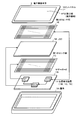
- FIG. 2 is an exploded perspective view for explaining a configuration example of the electronic device main body 1 configured by using the position detection device of the present invention.
- a mother board 1 ⁇ / b> B, a first sensor unit 1 ⁇ / b> C, an LCD 1 ⁇ / b> D, and a second sensor unit 1 ⁇ / b> E are stacked (superposed) in order from the housing 1 ⁇ / b> A side.
- the front panel 1F is formed by sealing the housing 1A.
- the LCD 1D has a display screen on the front panel 1F side.
- the motherboard 1B and the first sensor unit 1C are disposed below the LCD 1D, that is, on the side opposite to the display screen of the LCD 1D, and the second sensor unit 1E is disposed on the display screen side of the LCD 1D. Be placed.
- the first sensor unit 1C is an electromagnetic induction type position detection sensor
- the second sensor unit 1E is a capacitance type position detection sensor.
- the motherboard 1B, the first sensor unit 1C, and the second sensor unit 1E constitute the position detection device 1X of this embodiment.
- the first sensor unit 1C and the second sensor unit 1E have at least a detection area (not shown) in which both sensors can detect the position indicator 2 or a finger of a hand as a display area (not shown) of the display screen of the LCD 1D.
- the position on the operation area of the first sensor unit 1C, the position on the display screen of the LCD 1D, and the position on the operation area of the second sensor unit 1E are overlapped. It corresponds to one to one. Since the second sensor unit 1E is disposed at a position facing the display screen side of the LCD 1D, a transparent substrate is used.
- the front panel 1F is provided with an opening 1FW, and the display screen of the LCD 1D can be viewed from the opening 1FW via the second sensor 1E.
- a protective plate (not shown) such as transparent glass is disposed in the opening 1FW of the front panel 1F.
- the opening 1FW portion is operated by the position indicator 2 or the finger of the user's hand, and the operation of the indicated position is accepted through the first sensor unit 1C or the second sensor unit 1E. It also functions as an operation area 1FW.
- the motherboard 1B is provided with a control circuit CT1 for the first sensor unit 1C and a control circuit CT2 for the second sensor unit.
- the control circuit CT1 controls the first sensor unit 1C and detects the position and writing pressure operated by the user's position indicator 2 based on the output signal from the first sensor unit 1C. 1 function as a detection means.
- the control circuit CT2 controls the second sensor unit 1E, and detects a position where an operation with a finger of the user's hand or the like is performed based on an output signal from the second sensor unit 1E. Functions as a means.
- the motherboard 1B is provided with a display control circuit CT3 for performing display control on the LCD 1D based on output signals from the control circuits CT1 and CT2.
- the motherboard 1B is provided with various circuits such as a communication circuit.
- a so-called magnetic path plate may be provided between the motherboard 1B and the first sensor unit 1C.
- the magnetic path plate forms a magnetic path for the electromagnetic induction signal (alternating magnetic field) generated by each loop coil of the loop coil group provided in the first sensor unit 1C.
- the detection sensitivity of the indication position by the position indicator 2 can be improved by preventing the divergence of the magnetic flux generated by each loop coil.
- the magnetic path plate has a function of preventing radiation of the electromagnetic induction signal to the outside of the position detection device.
- the first sensor unit 1C is configured by stacking an X-axis direction loop coil group 111 and a Y-axis direction loop coil group 112.
- Each of the loop coil groups 111 and 112 is composed of, for example, 40 or more rectangular loop coils.
- the loop coils constituting the loop coil groups 111 and 112 are arranged so as to overlap each other at regular intervals.
- the first sensor unit 1C including the loop coil groups 111 and 112 includes a reception amplifier AP, an oscillation circuit unit 120, a position detection circuit unit 130, a writing pressure detection circuit unit 140, and a processing through a selection circuit 113 and a switch circuit SW.
- a control circuit CT1 including the control unit 150 is connected.
- An X-axis direction loop coil group 111 and a Y-axis direction loop coil group 112 are connected to the selection circuit 113.
- the selection circuit 113 selects an arbitrary loop coil from the two loop coil groups 111 and 112 under the control of the processing control unit 150 described later.
- the oscillation circuit unit 120 includes an oscillator 121 and a current driver 122.
- the oscillator 121 generates an AC signal having a frequency f0 and supplies the AC signal to a current driver 122 and a synchronous detector 141 of a writing pressure detection circuit unit 140 described later.
- the current driver 122 converts the AC signal supplied from the oscillator 121 into a current and sends the current to the switch circuit SW.
- the switch circuit SW switches the connection destination (transmission side terminal T, reception side terminal R) to which the loop coil selected by the selection circuit 113 is connected under the control of the processing control unit 150 described later.
- a current driver 122 is connected to the transmission side terminal T, and a reception amplifier AP is connected to the reception side terminal R.
- the induced voltage (reception signal) generated in the loop coil selected by the selection circuit 113 is sent to the reception amplifier AP via the selection circuit 113 and the switch circuit SW.
- the reception amplifier AP amplifies the induced voltage supplied from the loop coil and sends it to the detector 131 of the position detection circuit unit 130 and the synchronous detector 141 of the writing pressure detection circuit unit 140.
- the detector 131 of the position detection circuit unit 130 detects the induced voltage generated in the loop coil, that is, the received signal, and sends it to the low-pass filter 132.
- the low-pass filter 132 has a cutoff frequency sufficiently lower than the frequency f 0, converts the output signal of the detector 131 into a DC signal, and sends it to the sample hold circuit 133.
- the sample hold circuit 133 holds a voltage value at a predetermined timing of the output signal of the low-pass filter 132, specifically, a predetermined timing during the reception period, and sends it to an A / D (Analog-to-Digital) conversion circuit 134. .
- the A / D conversion circuit 134 converts the analog output of the sample hold circuit 133 into a digital signal and sends it to the processing control unit 150.
- the synchronous detector 141 of the writing pressure detection circuit unit 140 synchronously detects the output signal of the reception amplifier AP with an AC signal from the oscillator 121, and outputs a signal having a level corresponding to the phase difference between them to the low-pass filter 142.
- the low-pass filter 142 has a cutoff frequency sufficiently lower than the frequency f 0, converts the output signal of the synchronous detector 141 into a DC signal, and sends it to the sample hold circuit 143.
- the sample hold circuit 143 holds a voltage value at a predetermined timing of the output signal of the low-pass filter 142 and sends it to an A / D (Analog-to-Digital) conversion circuit 144.
- the A / D conversion circuit 144 converts the analog output of the sample hold circuit 143 into a digital signal and sends it to the processing control unit 150.
- the process control unit 150 controls each unit of the control circuit CT1 of the first sensor unit 1C. That is, the processing control unit 150 controls the selection of the loop coil in the selection circuit 113, the switching of the switch circuit SW, and the timing of the sample hold circuits 133 and 143. Based on the input signals from the A / D conversion circuits 134 and 144, the processing control unit 150 outputs signals (electromagnetic induction signals) from the X-axis direction loop coil group 111 and the Y-axis direction loop coil group 112 with a certain transmission duration. Send it.
- signals electromagnet induction signals
- An induced voltage is generated in each loop coil of the X-axis direction loop coil group 111 and the Y-axis direction loop coil group 112 by a signal transmitted from the position indicator 2.
- the processing control unit 150 calculates the coordinate value of the indicated position of the position indicator 2 in the X-axis direction and the Y-axis direction based on the voltage value of the induced voltage generated in each loop coil. Further, the processing control unit 150 detects the writing pressure based on the phase difference between the transmitted signal and the received signal.
- an electromagnetic induction type position detection sensor is realized by the first sensor unit 1C and the control circuit CT1 of this embodiment.
- the second sensor unit 1E is a so-called cross-point type capacitance (electrostatic coupling) type indication position detection sensor.
- a control circuit CT2 including a signal supply circuit 170, a signal reception circuit 180, and a control processing circuit 190 is connected to the second sensor unit 1E.
- the second sensor unit 1E is formed by laminating a transmission conductor group 161, an insulating layer, and a reception conductor group 162 in order from the lower layer side.
- the transmission conductor group 161 includes a plurality of linear transmission conductors 161X 1 , 161X 2 ,..., 161X m extending in the Y-axis direction and arranged in parallel with a predetermined interval therebetween.
- the reception conductor group 162 includes a plurality of linear reception conductors 162Y 1 , 162Y 2 extending in a direction intersecting the transmission conductors 161X 1 , 161X 2 ,..., 161X m (X-axis direction in FIG. 4). ,..., 161Y n are arranged in parallel with a predetermined distance from each other.
- a signal supply circuit 170 including a transmission signal supply circuit 171 and a clock generation circuit 172 is connected to the transmission conductor group 161.
- a signal receiving circuit 180 including an amplifier circuit 181, an A / D conversion circuit 182, and a pointing position detection circuit 183 is connected to the reception conductor group 162. These signal supply circuit 170 and signal reception circuit 180 are controlled by a control processing circuit 190.
- Different predetermined signals are supplied from the transmission signal supply circuit 171 to the second sensor unit 1E.
- This predetermined signal is supplied to each of the transmission conductors 161X 1 , 161X 2 ,..., 161X m at a timing according to the control of the control processing circuit 190 and the clock signal from the clock generation circuit 172.
- the transmission signal supply circuit 171 supplies a signal having a different frequency for each transmission conductor, or generates and supplies a signal whose phase is shifted for each transmission conductor from a signal of a predetermined coding pattern, A signal with a different code pattern is supplied for each transmission conductor.
- the current flowing through the indicator changes the current flowing through the cross point.
- indicated by the indicator can be detected now by detecting the cross point where an electric current changes.
- signals received by the reception conductors 162Y 1 , 162Y 2 ,..., 162Y n are amplified by the amplification circuit 181 and converted into digital signals by the A / D conversion circuit 182.
- the designated position detection circuit 183 is supplied.
- the designated position detection circuit 183 is supplied to each of the transmission conductors 161X 1 , 161X 2 ,..., 161X m with respect to the digital signal supplied from the A / D conversion circuit 182 under the control of the control processing circuit 190.
- By performing arithmetic processing according to a predetermined signal a current change at each cross point is detected.
- the transmission conductors 161x 1 from the transmission signal supplying circuit 171, 161x 2, ..., when the signal of the frequency multiplexing method is used as a signal supplied to each of 161x m is an instruction position detecting circuit 183
- each transmission conductors 161x 1 from the transmission signal supplying circuit 171, 161X 2, ... by performing the synchronous detection operation using the signals having the same frequency as the signal supplied to 161x m, detects a signal of a frequency of interest.
- the indicated position detection circuit 183 operates in accordance with the control of the control processing circuit 190 and detects the position indicated by the indicator.
- the designated position detection circuit 183 operates according to the control of the control processing circuit 190, and detects the designated position by the indicator based on the calculated correlation calculation value.
- the second sensor unit 1E has a configuration in which a plurality of cross points are provided.
- the detected position can be detected (multi-point detection).
- the invention of the cross-point type electrostatic coupling type indicator detection device using the frequency multiplexing method is disclosed in Japanese Patent Application Laid-Open No. 2011-3035, and the cross-point type electrostatic coupling using the phase shift method is disclosed.
- An invention relating to the indicator detection device of the type is disclosed in Japanese Patent Application Laid-Open No. 2011-3036.
- An invention of a cross-point type electrostatic coupling type indicator detection device using a code multiplexing method is disclosed in Japanese Patent Application Laid-Open No. 2011-128982.
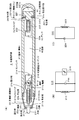
- FIG. 5 (A) shows the entire configuration of the position indicator 2 formed in a pen shape, and the housing 21 and the like shown by hatching are cut into the rear side and the front side and the front side. Is shown, and the internal structure is visible.
- 5B and 5C show an equivalent circuit of a circuit portion formed at the end portion of the position indicator 2.
- the position indicator 2 includes a housing 21 formed of a conductive material (conductor) such as aluminum.
- the casing 21 is a cylindrical member having a hollow portion 21a, and an opening 21b is formed on one end side in the longitudinal direction.
- One end side of the casing 21 provided with the opening 21b is formed of a non-conductive material (insulator) such as ABS resin, for example, and has a frustoconical tip 22 having an opening 22a and a hollow portion 22b. Is provided.
- the distal end portion 22 has a diameter that decreases toward the end portion 22c, and the position indicator 2 is formed in a pen shape by the distal end portion 22 and the housing 21.
- a convex portion 22 d is formed at the end portion 22 c of the distal end portion 22 so as to protrude toward the inside of the opening 22 a of the distal end portion 22.
- the core body 211 Since the core body 211 is used in contact with the operation area 1FW of the electronic apparatus main body 1, it is formed of a non-conductive synthetic resin such as polyacetal resin (Duracon) in consideration of resistance to friction. Yes. As shown in FIG. 5 (A), the core 211 is formed so as to protrude in a direction intersecting the axial direction of the pointing portion 211a and a bar-shaped pointing portion 211a having a hemispherical tip. The locking portion 211b is locked to the convex portion 22d, and the shaft portion 211c is formed to extend from the locking portion 211b in the direction opposite to the pointing portion 211a. The core body 211 is disposed inside the housing 21 such that the instruction part 211a protrudes from the opening part 22a of the distal end part 22.
- a non-conductive synthetic resin such as polyacetal resin (Duracon) in consideration of resistance to friction.
- the core 211 is inserted into a cylindrical ferrite core 212 in which the shaft portion 211 c is disposed inside the housing 21, and the writing pressure at which the end portion 221 d of the shaft portion 211 c is provided in the housing 21. It arrange
- the core body 211 slides toward the tip portion 22 side by the weight of the core body 211 and the repulsive force of the variable capacitor 215. At this time, the core 211 has the locking portion 211b locked to the convex portion 22d of the distal end portion 22 so that the core 211 protrudes excessively or the core 211 comes out of the housing 21. There is no such thing.
- a coil 213 is wound around the ferrite core 212.
- a capacitor 214 and a variable capacitor 215 are connected to the coil 213 in parallel.
- the coil 213, the capacitor 214, and the variable capacitor 215 form a resonance circuit 210 shown in FIG. 5B on one end side of the housing 21, and the transmission signal from the first sensor unit 1 ⁇ / b> C described above is formed.
- a resonating reflected signal (resonant signal) is generated and transmitted to the first sensor unit 1C.
- the resonance circuit 210 shown in FIG. 5B includes a variable capacitor 215 whose capacitance value changes in accordance with the pressing force applied to the core body 211. Therefore, the electrostatic capacitance of the variable capacitor 215 A reflected signal reflecting the change in capacitance is generated and transmitted toward the first sensor unit 1C.
- the first sensor unit 1C and its control circuit CT1 detect the position where the reflected signal is received and the change in the reflected signal caused by the change in capacitance (for example, a minute change in the frequency of the reflected signal). The indicated position and writing pressure on the sensor unit 1C can be detected.
- a cap holding portion 23 is provided on the other end side of the casing 21 so as to protrude in the axial direction of the casing 21.
- the cap holding portion 23 is provided with an engagement receiving portion 23 a formed so as to be recessed in the radial direction of the housing 21.
- maintenance part 23 is formed with an electroconductive material similarly to the housing
- the cap holding part 23 formed separately from the housing 21 can be adhered to the housing 21 by welding or the like.
- the cap holding part 23 is covered with a cap 221 made of, for example, conductive rubber (conductive rubber).
- the cap 221 is an elastic body having a hemispherical tip and an opening 221a formed at the rear end.
- the cap 221 has a hollow portion 221b and an engaging portion formed so as to protrude in the radial direction of the cap 221. 221c.
- the cap 221 is attached to the housing 21 by the cap holding portion 23 being inserted into the hollow portion 221b from the opening 221a side, and the engagement portion 221c and the engagement receiving portion 23a of the cap holding portion 23 being engaged. It is done.
- the cap 221 is elastically deformed when pressed against the operation region 1FW, and the contact portion with the operation region 1FW is widened, so that detection of the position instruction by the second sensor can be facilitated more reliably. It is configured.
- a mounting portion 24 formed so as to protrude from the other end side of the housing 21 to the one end side is provided inside the housing 21, and the mounting portion 24 has a cylindrical shape.
- the ferrite core 222 is provided.
- the ferrite core 222 is a ferrite core similar to the ferrite core 212 provided on one end side, and is attached to the inside of the housing 21 by the attachment portion 24 being inserted into the cylindrical hole.
- a coil 223 is wound around the ferrite core 222.
- a capacitor 224 is connected in parallel to the coil 223.
- the resonance circuit 220 is configured by the coil 223 and the capacitor 224.
- the resonance circuit 220 shown in FIG. 5C generates a reflected signal that resonates with the transmission signal from the first sensor unit 1C described above, and can transmit the reflected signal toward the first sensor unit 1C. Yes.
- a cap 221 formed of conductive rubber is attached to the other end side of the position indicator 2, so that the indicated position can be detected by the second sensor unit 1E.
- the resonance circuit 220 including the coil 223 and the capacitor 224 has a configuration in which the indicated position can be detected also by the first sensor unit 1C. That is, the position indicated by using the side where the cap 221 of the position indicator 2 is provided is configured to be detectable by both the first sensor unit 1C and the second sensor unit 1E.
- the resonance frequency of the resonance circuit 210 provided on the core body 211 side and the resonance frequency of the resonance circuit 220 provided on the cap 221 side may be set to the same frequency.
- the resonance circuit 210 and the resonance circuit 220 do not necessarily need to be set to the same resonance frequency, and the resonance circuit 210 and the resonance circuit 220 can be set to different resonance frequencies.
- the electronic device main body 1 is equipped with a position detection device 1X having a first sensor unit 1C of an electromagnetic induction type and a second sensor unit 1E of an electrostatic induction type.
- the core 211 side of the position indicator 2 has a configuration in which the indicated position can be detected only by the first sensor unit 1C of the electromagnetic induction method, and the cap 221 side of the position indicator 2 has an electromagnetic induction. Since the position instructed by both the first sensor unit 1C of the system and the second sensor unit 1E of the electrostatic induction system can be detected, the operation by the position indicator 2 uses the core 211 side. In the case of using the cap 221 side, different information can be input. Specifically, the core 211 side of the position indicator 2 is used for inputting a locus, and the cap 221 side of the position indicator 2 is used for deleting the input locus.
- FIG. 6A shows the case of using the locus input function
- FIG. 6B shows the case of using the input locus erasing function (eraser function).
- 6A and 6B for the electronic device main body 1, the LCD 1D, the first sensor unit 1C provided across the LCD 1D, and the second sensor unit are shown.
- a portion related to the position detection apparatus 1X including 1E and control circuits CT1, CT2, and CT3 is shown.
- the reflected signal from the position indicator 2 is received by the loop coil in the vicinity of the position indicator 2, and the loop coil of the first sensor unit 1C is received. Inductive voltage is generated.
- the control circuit CT1 for the first sensor unit 1C detects (calculates) the coordinate value of the indicated position by the position indicator 2 based on the level of the voltage value of the induced voltage generated in each loop coil, and the position indicator 2 The pen pressure is detected based on the phase difference between the signal transmitted to the position indicator 2 and the reflected signal received from the position indicator 2.
- the control circuit CT1 supplies the detected indication position and writing pressure to the control circuit CT3 for display and the like.
- the display control circuit CT3 when an output signal is generated from the control circuit CT1 for the first sensor unit 1C and no output signal is generated from the control circuit CT2 for the second sensor unit 1E, the display control circuit CT3 is used. Is determined to be a trajectory input instruction. In this case, the display control circuit CT3 displays a trajectory of the thickness corresponding to the writing pressure at the indicated position in accordance with the indication position and the writing pressure from the control circuit for the first sensor unit 1C. Processing to be displayed on the part.
- the reflected signal from the position indicator 2 is received by the loop coil near the position indicator 2, and an induced voltage is generated in the loop coil of the first sensor unit 1C.
- the control circuit CT1 for the first sensor unit 1C detects (calculates) the coordinate value of the indicated position by the position indicator 2 based on the level of the voltage value of the induced voltage generated in each loop coil. Since there is no variable pressure capacitor for detecting the pen pressure on the second end side of the position indicator 2, the pen pressure cannot be detected.
- the control circuit CT1 supplies a signal indicating the detected indicated position to the display control circuit CT3.
- the housing 21, the cap holding part 23, and the cap 221 are all conductors (conductive members).
- the cap 221 of the position indicator 2 held in the user's hand is brought into contact with the operation area 1FW of the electronic device main body 1, whereby the position where the cap 221 is placed on the second sensor unit 1E.
- the current at the crossing point changes as the current is shunted through the position indicator 2.
- the control circuit CT2 for the second sensor unit 1E detects the cross point where the current is changing, thereby detecting the second indicated by the position indicator 2.
- the position on the sensor unit 1E can be detected.
- the control circuit CT2 supplies an output signal indicating the detected designated position (position information) to the display control circuit CT3.
- the control circuit for display and the like CT3 determines that it is an instruction to delete the already input locus.
- the display control circuit CT3 performs a process of erasing the locus existing at the designated position on the LCD 1D in accordance with the position information from the control circuit CT2 for the second sensor unit 1E.
- a locus such as a point or a line can be input, and a detailed diagram can be input. Fine drawing information can be input.
- the target portion of the already input locus can be deleted. Therefore, the target operation can be performed on the electronic device main body 1 without taking time and effort to switch the locus input mode and the locus erasing mode on the electronic device main body 1.
- the position indicator 2 is provided with a resonance circuit having a different resonance frequency at each of both ends, as in a conventional pen-type position indicator, or in a resonance circuit provided at each of both ends, There is no need to take action such as reversing. Also, no pen pressure detection means such as a variable capacitor is provided at each end of the pen-type position indicator. The means for detecting the writing pressure may be provided only on the side of the core body 211 used for inputting the locus. As a result, the configuration of the position indicator 2 can be simplified as compared with the conventional position indicator.
- the position detection device 1X mounted on the electronic device main body 1 as in the case of using a conventional position indicator, which end portion of the position indicator is directed to the own device is received. There is no need to perform processing such as discrimination from the frequency of the signal. That is, in the case of the position detection device 1X of this embodiment, whether the locus is input according to the presence or absence of the output signals from the first control circuit CT1 and the second control circuit CT2. It is possible to appropriately determine whether the input locus is to be deleted. Therefore, it is necessary to perform complicated processing such as whether to input the locus or to delete the input locus based on discrimination of the frequency of the reflected signal from the position indicator. It can be realized without.
- the resonance circuits 210 and 220 mounted on the position indicator 2 are provided. Since it is not detected, the operation of the user is detected only by the second sensor unit 1E, and the operation is not detected by the first sensor unit 1C. Therefore, in this case, the display control circuit CT3 can accept the input of the locus based on the output signal from the control circuit CT2 for the second sensor unit 1E. That is, it is possible to accept an operation on an icon or a display button corresponding to the designated position and to execute a process corresponding to the selected icon or display button.
- FIG. 7 is a flowchart for explaining processing executed by the display control circuit CT3 shown in FIGS.
- the process of the flowchart shown in FIG. 7 is a process that is always executed by the display control circuit CT3 when the electronic apparatus main body 1 is powered on.
- the display control circuit CT3 first determines whether or not there is an output signal from the control circuit CT1 for the first sensor unit 1C (step S101). When it is determined in step S101 that there is an output signal from the control circuit CT1 (in the case of Y in step S101), the display control circuit CT3 outputs from the control circuit CT2 for the second sensor unit 1E. It is determined whether or not there is a signal (step S102).
- step S102 it is determined in step S102 that there is an output signal from the control circuit CT2 (in the case of Y in step S102).
- the display control circuit CT3 uses the cap 221 side of the position indicator 2 to the electronic device main body 1. It is determined that an instruction is input.
- the display control circuit CT3 determines that the operation being performed on the electronic device main body 1 is an instruction to erase the input locus. Then, the display control circuit CT3 of this embodiment performs an erasing process of the locus displayed (drawn) at the designated position (designated position) based on the output signal from the second sensor unit 1E. (Step S103). Thereafter, the display control circuit CT3 repeats the processing from step S101.
- the cap 221 on the second end side of the position indicator 2 is made of conductive rubber, and the area in contact with the operation region 1FW is also somewhat wide. For this reason, it is not necessary to detect the writing pressure or the like, and it is possible to easily specify the erasing range (already input locus) desired by the user. Moreover, even if the locus remains unerased, the intended locus can be erased by performing another operation using the second end side (cap 221 side) of the position indicator 2.
- the display control circuit CT3 determines that there is no output signal from the control circuit CT2 (in the case of N in step S102). In this case, since only the output signal from the control circuit CT1 is supplied, the display control circuit CT3 uses the core 211 side of the position indicator 2 to operate the electronic device main body 1. It is determined that it is being performed. For this reason, the display control circuit CT3 determines that the operation being performed on the electronic device main body 1 is an input of the locus, and the locus input process based on the output signal from the first sensor unit 1C. Is performed (step S104). Thereafter, the display control circuit CT3 repeats the processing from step S101.
- step S101 when it is determined in step S101 that the output signal from the control circuit CT1 is not present (N in step S101), the display control circuit CT3 controls the second sensor unit 1E. It is determined whether or not there is an output signal from the circuit CT2 (step S105). In the determination process in step S105, it is assumed that the display control circuit CT3 determines that there is an output signal from the control circuit CT2 (in the case of Y in step S105). In this case, since only the output signal from the control circuit CT2 is supplied, the display control circuit CT3 does not use the position indicator 2 but the user's hand finger or a capacitance type device, for example. It is determined that an operation is performed on the electronic device main body 1 with the dedicated pen (position indicator) for the sensor.
- the display control circuit CT3 determines that the operation being performed on the electronic device main body 1 is an input of the locus, and the locus input process based on the output signal from the second sensor unit 1E. Is performed (step S106). In this case, in addition to execution of processing according to selection of an icon or a display button, drawing using a finger or a dedicated pen for a capacitive sensor can be performed. Thereafter, the display control circuit CT3 repeats the processing from step S101.
- step S105 it is determined that there is no output signal from the control circuit CT2 (in the case of N in step S105). In this case, since no output signal is supplied from either the control circuit CT1 or the control circuit CT2, the display control circuit CT3 determines that the operation area 1FW of the electronic device body 1 is not operated. The The display control circuit CT3 does not perform display control and repeats the processing from step S101.
- the function related to the operation can be automatically switched depending on how the position indicator 2 is used. That is, when an operation is performed using the core 211 side of the position indicator 2, a locus input process is performed, and when an operation is performed using the cap 221 side of the position indicator 2, It is possible to delete the input locus. In this case, the user does not switch the input mode for the position detection device 1X. Also, both the operation using the position indicator 2 and the operation on the first sensor unit 1C of the capacitance type using the finger of the user's hand can be appropriately received and processed.
- a position indicator 2A which is a modification of the position indicator 2, will be described with reference to FIG.
- parts that are configured in the same manner as the position indicator 2 shown in FIG. 5 are given the same reference numerals, and descriptions thereof are omitted.
- the position indicator 2 has a configuration in which the resonance circuit 210 is provided on the core body 211 side and the resonance circuit 220 is provided on the cap 221 side.
- the configuration of the position indicator of the present invention is not limited to this.
- the resonance circuit 210 provided on the core 211 side generates a sufficiently strong magnetic field when the cap 221 side is used in contact with the operation region 1FW. In this case, it is not necessary to provide a resonance circuit on the cap 221 side.
- the position indicated by the position indicator 2A can be detected by the second sensor unit 1E of the electronic device main body 1 through the position indicator 2A. Further, the reflected signal generated by the resonance circuit 210 mounted on the position indicator 2A can be detected by the first sensor unit 1C of the electronic device main body 1.
- the cap 221 side of the position indicator 2A is used in contact with the operation region 1FW of the electronic device body 1, the resonance circuit 210 of the position indicator 2A and the first sensor unit 1C of the electronic device body 1 are used. And the distance will be longer. For this reason, it is difficult to specify the position instructed in a narrow range on the first sensor unit 1C as in the case of inputting the trajectory using the core 211 side of the position indicator 2A. However, since a sufficiently strong magnetic field is generated, it can be detected that the position indicator 2A is positioned on the first sensor unit 1C.
- the cap 221 side of the position indicator 2A in which no resonance circuit is provided on the cap 221 side is used in contact with the operation area 1FW of the electronic device body 1, the first sensor unit 1C and By detecting the position indicated by the position indicator 2A in both the second sensor unit 1E, as in the case described with reference to FIG. The locus can be erased.
- the position indicator 2A shown in FIG. 8 when the operation is performed by bringing the core 211 side of the position indicator 2A shown in FIG. 8 into contact with the operation area 1FW of the electronic device main body 1, the position indicator is only used in the first sensor unit 1C. The indicated position by 2A can be detected. Therefore, when the operation is performed by bringing the core 211 side of the position indicator 2A into contact with the operation region 1FW of the electronic device main body 1, the locus is the same as in the case described with reference to FIG. Can be input. In the case of the position indicator 2A shown in FIG. 8, the configuration can be further simplified as compared with the position indicator 2 described with reference to FIG.
- the 1st sensor part 1C mounted in the electronic device main body 1 of embodiment mentioned above is an electromagnetic induction type sensor.
- a signal is transmitted from the first sensor unit 1C of the electronic device main body 1, and the reflection signal (resonance signal) generated by the resonance circuits 210 and 220 of the position indicator 2 according to the signal. Is received by the first sensor unit 1C.
- the position indicator itself includes a signal generation circuit that generates the same signal as the reflected signal, the first sensor unit 1C can be configured not to transmit a signal to the position indicator.
- a position indicator 2B which is a modification of the position indicator 2, will be described with reference to FIG.
- the position indicator 2B of this example the position indicator 2B itself includes a signal generation circuit 230, and the signal generation circuit 230 is connected to both the resonance circuit 210 and the resonance circuit 220.
- the signal generation circuit 230 includes a power supply circuit including an oscillator and a battery that generate a signal having a predetermined frequency. Except for the point that the signal generation circuit 230 is provided, the other parts are configured in the same manner as the position indicator 2 of the embodiment described above with reference to FIG. For this reason, in the position indicator 2B of FIG. 9, the same reference numerals are assigned to the same components as those of the position indicator 2 shown in FIG.
- the position indicator 2B of this example is also used by bringing the core 211 side into contact with the operation region 1FW of the electronic device main body 1.
- the locus can be input through the first sensor unit 1C.
- the position indicator 2B is detected only by the first sensor unit 1C.
- the cap 221 side of the position indicator 2B is used in contact with the operation area 1FW of the electronic device main body 1, the first sensor unit 1C and the second sensor unit are used. Since it is detected by both 1E and 1E, the locus already input can be deleted as in the case of using the position indicator 2 of the embodiment described above.
- the current driver 122 and the switch circuit SW corresponding to the first sensor unit 1C and the control circuit CT1 shown in FIG. 3 are not provided.
- the contents of control by the processing control unit 150 can be simplified.
- the cap 221 side of the position indicators 2, 2A, 2B is designated by contacting the position on the operation area 1FW corresponding to the display position of the portion for which the attribute of the locus already input is to be changed. Then, by using the cap 221 side of the position indicators 2, 2A, 2B, for example, by performing a tap operation on the specified portion, the line type of the trajectory is changed sequentially or the thickness of the trajectory is changed according to the tap operation. Or change the color of the trajectory.
- the electronic device main body 1 it is also possible to select in the electronic device main body 1 what to change the trajectory attributes first.
- the trajectory attribute is set to “thin dotted line”. Then, using the second end side (cap 221 side) of the position indicators 2, 2A, 2B, when the part for which the attribute of the already input locus is to be changed is designated, the locus portion is selected immediately. Can be changed to an attribute.
- the second sensor unit 1E is of the electrostatic capacity type.
- the capacitive position detection sensor can be operated using a so-called stylus pen with a conductive rubber or conductive cloth at the tip.
- the cap 221 side of the position indicator 2 is used in contact with the operation area 1FW.
- the reflected signal from the resonance circuit 220 of the position indicator 2 is received by the first sensor unit 1C, and the position indicator 2 is detected by the first sensor unit 1C.
- the second sensor unit 1E is electrically connected to the user having the position indicator 2 through the casing 21, the cap holding part 23, and the cap 221 of the position indicator 2, whereby the second sensor.
- the position indicator 2 is also detected in the part 1E.
- the display control circuit CT3 indicates a position where the position where the position indicator 2 is detected through the first sensor unit 1C and the position where the position indicator 2 is detected through the second sensor unit 1E overlap. The position is recognized as instructed by the user, and an input of a locus is accepted.
- the locus is appropriately input even if the user's palm is in contact with the operation area 1FW. Yes. That is, for example, when the palm contacts the operation area 1FW, the first sensor unit 1C cannot detect the contact position even though the second sensor unit 1E can detect the contact position. This is because it can be controlled not to accept as an appropriate input.
- the combined use of the first and second sensor units 1C and 1E can reduce the on-load of contact detection for the operation area 1FW such as the position indicator 2.
- the position indicator 2A described with reference to FIG. 8 when used, the same operation can be basically performed. However, since the position indicator 2A includes only the resonance circuit 210, the resonance indicator 210 It is necessary that the position indicated by the transmission signal does not reach the contact portion of the palm.
- the second sensor unit 1E has been described as a capacitive type. Accordingly, the second sensor unit 1E can use a surface-type capacitive position detection sensor in addition to a projection-type capacitive position detection sensor. That is, as the second sensor unit 1E, various capacitance type position detection sensors can be used.
- the first sensor unit 1C can also use various electromagnetic induction type position detection sensors.
- a resistive film type position detection sensor or a surface acoustic wave type position detection sensor may be used as the second sensor unit 1E.
- the input device including the position detection device and the position indicator according to the present invention is applied to a tablet PC or a high-function mobile phone terminal having a display device such as an LCD will be described as an example.
- the present invention can also be applied to an input device such as a so-called digitizer that does not include a display device that is connected to an electronic device such as a personal computer.
- the function of the first sensor in the claims is realized by the first sensor unit 1C, and the second sensor is realized by the second sensor unit 1E. Further, the function of the first indicating means in the claims is realized by the resonance circuits 210 and 220 of the position indicator, and the second indicating means is realized mainly by the cap 221 of the position indicator.
- the function of the first detection means in the claims is realized by the control circuit CT1
- the function of the second detection means is realized by the control circuit CT2
- the function of the control means is realized by the display control circuit CT3. ing.
- the processing executed by the display control circuit CT3 shown in FIG. 7 corresponds to the input control method of the position detection apparatus according to the present invention.
- 7 is an input control program corresponding to the input control method of the position detection apparatus according to the present invention, and is executed by the display control circuit CT3. Program.
Landscapes
- Engineering & Computer Science (AREA)
- General Engineering & Computer Science (AREA)
- Theoretical Computer Science (AREA)
- Physics & Mathematics (AREA)
- Human Computer Interaction (AREA)
- General Physics & Mathematics (AREA)
- Electromagnetism (AREA)
- Position Input By Displaying (AREA)
- User Interface Of Digital Computer (AREA)
Abstract
Description
位置指示器と当該位置指示器を用いた情報の入力を受け付ける位置検出装置とからなる入力装置であって、
前記位置検出装置は、
第1のセンサと、
前記第1のセンサに対して重畳配置され、前記第1のセンサとは異なる検出方式の第2のセンサと、
前記第1のセンサからの出力に基づいて、少なくとも位置指示器の存在を検出する第1の検出手段と、
前記第2のセンサからの出力に基づいて、少なくとも位置指示器の存在を検出する第2の検出手段と、
前記第1、第2の検出手段からの出力信号の供給を受けて、前記第1、第2の検出手段のいずれか一方から出力信号の供給を受けている場合と、前記第1、第2の検出手段の両方から出力信号の供給を受けている場合とで、当該出力信号に応じた処理内容を変える制御手段と、
を備え、
前記位置指示器は、
略筒状の筐体と、
前記筐体の両方の端部には、それぞれ前記第1のセンサにより少なくとも当該位置指示器の存在を検出可能にするための第1の指示手段と、
前記筐体の一方の端部には、当該一方の端部を前記位置検出装置に接触させた場合に、前記第2のセンサにより少なくとも当該位置指示器の存在を検出可能にするための第2の指示手段と
を備えることを特徴とする。 In order to solve the above problems, the input device of the invention according to this application is:
An input device comprising a position indicator and a position detection device that receives input of information using the position indicator,
The position detection device includes:
A first sensor;
A second sensor having a detection method different from that of the first sensor, which is superimposed on the first sensor;
First detection means for detecting the presence of at least a position indicator based on an output from the first sensor;
Second detection means for detecting at least the presence of a position indicator based on the output from the second sensor;
A case where an output signal is supplied from one of the first and second detection means and an output signal is supplied from one of the first and second detection means; Control means for changing the processing content according to the output signal when the output signal is supplied from both of the detection means,
With
The position indicator is
A substantially cylindrical housing;
At both ends of the housing, first indication means for enabling at least the presence of the position indicator to be detected by the first sensor,
A second end for enabling at least the presence of the position indicator to be detected by the second sensor when the one end is brought into contact with the position detection device. And an instruction means.
この発明に係る位置検出装置と位置指示器とからなる入力装置が搭載されて構成された電子機器の一例を、図1を参照して説明する。この例の電子機器は、例えばLCD(Liquid Crystal Display)などの表示装置を備えるタブレットPCや高機能携帯電話端末であり、位置検出装置が搭載された電子機器本体1と、ペン形状の位置指示器2とからなる。 [Specific examples of electronic devices]
An example of an electronic apparatus having an input device including a position detection device and a position indicator according to the present invention will be described with reference to FIG. The electronic device in this example is a tablet PC or a high-function mobile phone terminal provided with a display device such as an LCD (Liquid Crystal Display), for example, an electronic device
この発明の位置検出装置が用いられる電子機器本体1の構成例について、図2を参照して説明する。図2は、この発明の位置検出装置が用いられて構成された電子機器本体1の構成例を説明するための分解斜視図である。電子機器本体1は、筐体1Aの内部に、筐体1A側から順に、マザーボード1Bと、第1のセンサ部1Cと、LCD1Dと、第2のセンサ部1Eとが積層配置(重畳配置)され、フロントパネル1Fが筐体1Aを封止して形成される。 [Configuration Example of Electronic Device Body 1]
A configuration example of the electronic device
電子機器本体1に搭載される電磁誘導方式の第1のセンサ部1Cとその制御回路CT1の構成例について、図3を参照して説明する。第1のセンサ部1Cは、X軸方向ループコイル群111と、Y軸方向ループコイル群112とを積層させて設けることにより構成されている。各ループコイル群111,112は、例えば、それぞれ40本以上の矩形のループコイルからなっている。各ループコイル群111,112を構成する各ループコイルは、等間隔に並んで順次重なり合うように配置されている。 [Configuration Example of
A configuration example of the electromagnetic induction
電子機器本体1に搭載される静電容量方式の第2のセンサ部1Eとその制御回路CT2の構成例について、図4を参照して説明する。第2のセンサ部1Eは、いわゆるクロスポイント型静電容量(静電結合)方式の指示位置検出センサである。当該第2のセンサ部1Eには、信号供給回路170と信号受信回路180と制御処理回路190とからなる制御回路CT2が接続されている。 [Configuration Example of Second Sensor Unit 1E and Control Circuit CT2]
A configuration example of the capacitance type second sensor unit 1E mounted on the
この実施の形態の位置指示器2の構成例について、図5を参照して説明する。ここで、図5(A)はペン形状に形成される位置指示器2の全体構成を示すものであり、斜線を付して示した筐体21等は後側と前側とに切断して前側を取り除き、内部構造が視認できるようにした状態を示している。図5(B)、(C)は位置指示器2の端部部分に形成される回路部の等価回路を示している。 [Configuration Example of Position Indicator 2]
A configuration example of the
上述した構成を有する電子機器本体1と位置指示器2との具体的な利用態様について説明する。電子機器本体1には、電磁誘導方式の第1のセンサ部1Cと静電誘導方式の第2のセンサ部1Eとを有する位置検出装置1Xが搭載されている。また、位置指示器2の芯体211側は、電磁誘導方式の第1のセンサ部1Cでのみ、指示した位置の検出可能な構成を有し、位置指示器2のキャップ221側は、電磁誘導方式の第1のセンサ部1Cと静電誘導方式の第2のセンサ部1Eとの両方で指示した位置の検出可能な構成を有するので、位置指示器2による操作は、芯体211側を用いる場合とキャップ221側を用いる場合とでは、異なる情報の入力ができる。具体的には、位置指示器2の芯体211側は軌跡の入力用に用いられ、位置指示器2のキャップ221側は入力した軌跡の消去用に用いられる。 [Usage of
Specific usage modes of the electronic apparatus
電子機器本体1に対して、点や線などの軌跡を入力しようとする場合には、図6(A)に示すように、位置指示器2の芯体211の指示部211aを電子機器本体1の操作領域1FWに接触させる。そして、目的とする点や線を描くように位置指示器2を当該操作領域1FW上で移動させる。この場合、位置指示器2のコイル213とコンデンサ214と可変容量コンデンサ215とからなる共振回路210が機能し、第1のセンサ部1Cから送信されてくる送信信号に共振して反射信号を発生させ、これを第1のセンサ部1Cに送信する。 [Track input function]
When a locus such as a point or a line is to be input to the electronic device
電子機器本体1に対して、入力された軌跡を消去しようとする場合には、図6(B)に示すように、位置指示器2のキャップ221を電子機器本体1の操作領域1FW上の消去したい軌跡の表示位置に接触させることにより行う。そして、消去したい軌跡部分をなぞるように位置指示器2を当該操作領域1FW上で移動させる。この場合、位置指示器2のコイル223とコンデンサ224とからなる共振回路220が機能し、第1のセンサ部1Cから送信されてくる信号に共振して反射信号を発生し、この反射信号が第1のセンサ部1Cに送信される。 [Track erase function]
When it is intended to delete the input locus for the electronic device
次に、この実施の形態の電子機器本体1に搭載されている表示等制御回路CT3で行われる処理についてまとめる。図7は、図2、図6に示した表示等制御回路CT3が実行する処理を説明するためのフローチャートである。図7に示すフローチャートの処理は、電子機器本体1に電源が投入されている場合において、表示等制御回路CT3により常時実行されている処理である。 [Summary of Operation of Display Control Circuit CT3]
Next, the processing performed by the display control circuit CT3 mounted on the electronic device
位置指示器2の変形例である位置指示器2Aについて、図8を用いて説明する。なお、図8に示した位置指示器2Aおいて、図5に示した位置指示器2と同様に構成される部分には、同じ参照符号を付し、その部分の説明は省略する。 [
A
上述した実施の形態の電子機器本体1に搭載されている第1のセンサ部1Cは、電磁誘導方式のセンサである。そして、上述した実施の形態では、電子機器本体1の第1のセンサ部1Cから信号を送信し、当該信号に応じて位置指示器2の共振回路210、220が発生させる反射信号(共振信号)を第1のセンサ部1Cで受信する構成になっていた。しかし、位置指示器自体がこの反射信号と同じ信号を発生させる信号発生回路を備えていれば、第1のセンサ部1Cから位置指示器に対し信号を送信しない構成とすることができる。 [
The
なお、上述した実施の形態では、位置指示器2、2A、2Bの芯体211側を操作領域1FW上に接触させたときには、電磁誘導方式の第1のセンサ部1Cでのみ位置指示器が検出できることを利用して軌跡の入力処理を行うにした。また、位置指示器2、2A、2Bのキャップ221側を操作領域1FW上に接触させたときには、電磁誘導方式の第1のセンサ部1Cと静電容量方式の第2のセンサ部1Eとの両方で位置指示器が検出できることを利用して軌跡の消去処理を行うようにした。しかし、いずれのセンサにより検出されたかにより実行される処理は、これらに限るものではない。以下に、位置指示器2、2A、2Bを用いた情報の入力に関する他の利用態様について説明する。 [Other usage modes]
In the above-described embodiment, when the
位置指示器2、2A、2Bを用いて、軌跡の入力と、軌跡の属性の変更とを行うようにすることができる。例えば、位置指示器2、2A、2Bの芯体211側を操作領域1FW上に接触させて使用したときには、第1のセンサ部1Cでのみ指示位置が検出できる。この場合には、上述した実施の形態の場合と同様に軌跡の入力処理を行えるようにする。そして、位置指示器2、2A、2Bのキャップ221側を電子機器本体1の操作領域1FW上に接触させて使用したときには、第1のセンサ部1Cと第2のセンサ部1Eとの両方で指示位置を検出できる。この場合には、入力済みの軌跡の線種、線の太さ、色など、軌跡に対する属性の変更を行うようにする。 [Track input and attribute change for track]
By using the
また、第1のセンサ部1Cを通じて軌跡の入力を行うと共に、第2のセンサ部1Eを通じて適切に軌跡の入力を行うようにすることもできる。すなわち、上述した実施の形態では、第2のセンサ部1Eは静電容量方式のものである。静電容量方式の位置検出センサに対しては、先端に導電性のゴムや導電性の布を用いたいわゆるスタイラスペンを用いて操作を行うことができる。 [Track input using different sensor units]
Further, it is possible to input the trajectory through the
なお、上述した実施の形態において、第2のセンサ部1Eは静電容量方式のものとして説明した。したがって、第2のセンサ部1Eは、投影型の静電容量方式の位置検出センサの他、表面型の静電容量方式の位置検出センサを用いることができる。すなわち、第2のセンサ部1Eとしては、静電容量方式の種々の位置検出センサを用いることができる。また、第1のセンサ部1Cも、電磁誘導方式の種々の位置検出センサを用いることができる。 [Other variations]
In the above-described embodiment, the second sensor unit 1E has been described as a capacitive type. Accordingly, the second sensor unit 1E can use a surface-type capacitive position detection sensor in addition to a projection-type capacitive position detection sensor. That is, as the second sensor unit 1E, various capacitance type position detection sensors can be used. The
請求項における第1のセンサの機能は、第1のセンサ部1Cが実現し、第2のセンサは、第2のセンサ部1Eが実現している。また、請求項における第1の指示手段の機能は、位置指示器の共振回路210、220が実現し、第2の指示手段は、位置指示器の主にキャップ221が実現している。 [Others]
The function of the first sensor in the claims is realized by the
Claims (12)
- 検出方式の異なる第1及び第2のセンサを重畳配置して構成され、電子機器に接続または内蔵される位置検出装置に用いられる位置指示器であって、
略筒状の筐体と、
前記筐体の両方の端部には、それぞれ前記第1のセンサにより少なくとも当該位置指示器の存在を検出可能にするための第1の指示手段と、
前記筐体の一方の端部には、当該一方の端部を前記位置検出装置に接触させた場合に、前記第2のセンサにより少なくとも当該位置指示器の存在を検出可能にするための第2の指示手段と
を設けたことを特徴とする位置指示器。 A position indicator used in a position detection device configured by overlappingly arranging first and second sensors having different detection methods, connected to or incorporated in an electronic device,
A substantially cylindrical housing;
At both ends of the housing, first indication means for enabling at least the presence of the position indicator to be detected by the first sensor,
A second end for enabling at least the presence of the position indicator to be detected by the second sensor when the one end is brought into contact with the position detection device. A position indicator characterized by comprising: - 前記第1の指示手段は、前記筐体の一方の端部に加えられた圧力を検出するための検出手段を備えている、
ことを特徴とする請求項1に記載の位置指示器。 The first indicating means includes a detecting means for detecting a pressure applied to one end of the casing.
The position indicator according to claim 1. - 前記第1のセンサは、電磁誘導方式により前記位置指示器による操作を検出するためのセンサであり、
前記第1の指示手段は、前記第1のセンサに対し信号を供給するためのコイルを含む、
ことを特徴とする請求項2に記載の位置指示器。 The first sensor is a sensor for detecting an operation by the position indicator by an electromagnetic induction method,
The first indicating means includes a coil for supplying a signal to the first sensor,
The position indicator according to claim 2. - 前記コイルから前記信号を発生させるための信号発生手段を更に備え、
前記コイルは、前記信号発生手段から供給される信号に応じて前記信号を送出する、
ことを特徴とする請求項3に記載の位置指示器。 A signal generating means for generating the signal from the coil;
The coil sends out the signal in response to a signal supplied from the signal generating means.
The position indicator according to claim 3. - 前記第2のセンサは、静電容量方式により前記位置指示器による操作を検出するためのセンサであり、
前記第1の指示手段には、前記コイルにより前記信号の送信と前記第1のセンサからの信号の受信とを行う共振回路が形成されており、
前記第2の指示手段は、前記筐体の前記一方の端部に設けられた導電性部材を含む、
ことを特徴とする請求項4に記載の位置指示器。 The second sensor is a sensor for detecting an operation by the position indicator by a capacitance method,
In the first instruction means, a resonance circuit that performs transmission of the signal and reception of a signal from the first sensor by the coil is formed,
The second instruction means includes a conductive member provided at the one end of the housing.
The position indicator according to claim 4. - 前記第1の指示手段の前記コイルは、前記筐体の両方の端部のそれぞれに別個に設けられていることを特徴とする請求項2、請求項3、請求項4または請求項5のいずれかに記載の位置指示器。 6. The coil according to claim 2, 3, 4 or 5, wherein the coil of the first indicating means is provided separately at each of both ends of the casing. A position indicator according to crab.
- 2つの検出方式によりペン形状に形成された位置指示器に指示された位置を検出する位置検出装置であって、
前記2つの検出方式のうちの一方の検出方式により前記位置指示器による操作を検出するための第1のセンサと、
前記第1のセンサに対して重畳配置され、前記第1のセンサとは異なる他方の検出方式により前記位置指示器による操作を検出するための第2のセンサと、
前記第1のセンサからの出力信号に基づいて、少なくとも位置指示器の存在を検出する第1の検出手段と、
前記第2のセンサからの出力信号に基づいて、少なくとも位置指示器の存在を検出する第2の検出手段と、
前記第1、第2の検出手段からの出力信号の供給を受けて、前記出力信号に応じた処理を実行する制御手段と、を備え、
前記制御手段は、前記第1、第2の検出手段のうちの一方から 出力信号の供給を受けている場合と、前記第1、第2の検出手段の両方から出力信号の供給を受けている場合とで、当該出力信号に応じた処理内容を変える、
ことを特徴とする位置検出装置。 A position detection device that detects a position indicated by a position indicator formed in a pen shape by two detection methods,
A first sensor for detecting an operation by the position indicator by one of the two detection methods;
A second sensor arranged to overlap with the first sensor and for detecting an operation by the position indicator by another detection method different from the first sensor;
First detection means for detecting the presence of at least a position indicator based on an output signal from the first sensor;
Second detection means for detecting at least the presence of a position indicator based on an output signal from the second sensor;
Control means for receiving a supply of output signals from the first and second detection means and executing processing according to the output signals;
The control means receives an output signal from one of the first and second detection means and receives an output signal from both the first and second detection means. Depending on the case, change the processing content according to the output signal,
A position detecting device characterized by that. - 前記制御手段は、
前記第1、第2の検出手段のいずれか一方から出力信号の供給を受けている場合には、当該出力信号を、前記指示された位置に応じた軌跡の入力の操作として処理し、
前記第1、第2の検出手段の両方から出力信号の供給を受けている場合には、前記第1、第2の検出手段のいずれか一方の出力信号に基づいて前記指示された位置に応じた軌跡の入力の操作として処理するとともに、他方の出力信号を前記指示された位置に応じた前記軌跡についての属性に関する情報の入力として処理することを特徴とする請求項6に記載の位置検出装置。 The control means includes
When an output signal is supplied from one of the first and second detection means, the output signal is processed as an operation of inputting a locus according to the instructed position,
When the output signal is supplied from both the first and second detection means, the output position is determined based on the output signal of one of the first and second detection means. 7. The position detecting apparatus according to claim 6, wherein the position detection device is processed as an operation of inputting a trajectory, and the other output signal is processed as an input of information regarding an attribute of the trajectory according to the instructed position. . - 前記制御手段は、前記属性として、入力された前記軌跡についての消去の入力の操作として処理することを特徴とする請求項7に記載の位置検出装置。 The position detection apparatus according to claim 7, wherein the control unit processes the input as an erasure input operation as the attribute.
- 前記第1及び第2のセンサは、表示装置の表示面に対して積層されて電子機器に内蔵されている、ことを特徴とする請求項7に記載の位置検出装置。 The position detecting device according to claim 7, wherein the first and second sensors are stacked on a display surface of the display device and are built in an electronic device.
- 検出方式の異なる第1及び第2のセンサを重畳配置して構成され、電子機器に接続または内蔵される位置検出装置の前記第1及び第2のセンサからの出力信号の供給を受ける制御手段で用いられる制御方法であって、
前記第1、第2の検出手段のいずれか一方から出力信号の供給を受けている場合には、当該出力信号を、指示位置に応じた軌跡の入力の操作として処理する軌跡処理工程と、
前記第1、第2の検出手段の両方から出力信号の供給を受けている場合には、前記第1、第2の検出手段のいずれか一方の出力信号を、入力された前記軌跡についての属性に関する情報の入力として処理する属性処理工程と
を有することを特徴とする位置検出装置の入力制御方法。 Control means for receiving supply of output signals from the first and second sensors of a position detection device connected to or built in an electronic device, which is configured by superimposing first and second sensors having different detection methods. A control method used,
A trajectory processing step of processing the output signal as an input operation of a trajectory in accordance with the indicated position when an output signal is supplied from one of the first and second detection means;
When the output signal is supplied from both the first and second detection means, the output signal of one of the first and second detection means is set as an attribute of the input trajectory. An input processing method for a position detection apparatus, comprising: an attribute processing step for processing as an input of information regarding the position detection device. - 位置指示器と当該位置指示器を用いた情報の入力を受け付ける位置検出装置とからなる入力装置であって、
前記位置検出装置は、
第1のセンサと、
前記第1のセンサに対して重畳配置され、前記第1のセンサとは異なる検出方式の第2のセンサと、
前記第1のセンサからの出力に基づいて、少なくとも位置指示器の存在を検出する第1の検出手段と、
前記第2のセンサからの出力に基づいて、少なくとも位置指示器の存在を検出する第2の検出手段と、
前記第1、第2の検出手段からの出力信号の供給を受けて、前記第1、第2の検出手段のいずれか一方から出力信号の供給を受けている場合と、前記第1、第2の検出手段の両方から出力信号の供給を受けている場合とで、当該出力信号に応じた処理内容を変える制御手段と、
を備え、
前記位置指示器は、
略筒状の筐体と、
前記筐体の両方の端部には、それぞれ前記第1のセンサにより少なくとも当該位置指示器の存在を検出可能にするための第1の指示手段と、
前記筐体の一方の端部には、当該一方の端部を前記位置検出装置に接触させた場合に、前記第2のセンサにより少なくとも当該位置指示器の存在を検出可能にするための第2の指示手段と
を備えることを特徴とする入力装置。 An input device comprising a position indicator and a position detection device that receives input of information using the position indicator,
The position detection device includes:
A first sensor;
A second sensor having a detection method different from that of the first sensor, which is superimposed on the first sensor;
First detection means for detecting the presence of at least a position indicator based on an output from the first sensor;
Second detection means for detecting at least the presence of a position indicator based on the output from the second sensor;
A case where an output signal is supplied from one of the first and second detection means and an output signal is supplied from one of the first and second detection means; Control means for changing the processing content according to the output signal when the output signal is supplied from both of the detection means,
With
The position indicator is
A substantially cylindrical housing;
At both ends of the housing, first indication means for enabling at least the presence of the position indicator to be detected by the first sensor,
A second end for enabling at least the presence of the position indicator to be detected by the second sensor when the one end is brought into contact with the position detection device. An input device comprising:
Priority Applications (4)
| Application Number | Priority Date | Filing Date | Title |
|---|---|---|---|
| EP15818483.8A EP3168717A4 (en) | 2014-07-11 | 2015-03-10 | Position indicator, position detection device, and input control method for position detection device |
| CN201580032840.9A CN106462263B (en) | 2014-07-11 | 2015-03-10 | Position indicator, position detection device, and input control method for position detection device |
| JP2016532454A JP6544775B2 (en) | 2014-07-11 | 2015-03-10 | Position indicator, position detection device, input control method for position detection device, and input device |
| US15/379,369 US10073558B2 (en) | 2014-07-11 | 2016-12-14 | Position indicator, position detecting device, and input control method of position detecting device |
Applications Claiming Priority (2)
| Application Number | Priority Date | Filing Date | Title |
|---|---|---|---|
| JP2014143455 | 2014-07-11 | ||
| JP2014-143455 | 2014-07-11 |
Related Child Applications (1)
| Application Number | Title | Priority Date | Filing Date |
|---|---|---|---|
| US15/379,369 Continuation US10073558B2 (en) | 2014-07-11 | 2016-12-14 | Position indicator, position detecting device, and input control method of position detecting device |
Publications (1)
| Publication Number | Publication Date |
|---|---|
| WO2016006272A1 true WO2016006272A1 (en) | 2016-01-14 |
Family
ID=55063920
Family Applications (1)
| Application Number | Title | Priority Date | Filing Date |
|---|---|---|---|
| PCT/JP2015/056900 WO2016006272A1 (en) | 2014-07-11 | 2015-03-10 | Position indicator, position detection device, and input control method for position detection device |
Country Status (5)
| Country | Link |
|---|---|
| US (1) | US10073558B2 (en) |
| EP (1) | EP3168717A4 (en) |
| JP (1) | JP6544775B2 (en) |
| CN (1) | CN106462263B (en) |
| WO (1) | WO2016006272A1 (en) |
Cited By (13)
| Publication number | Priority date | Publication date | Assignee | Title |
|---|---|---|---|---|
| WO2017077382A1 (en) | 2015-11-06 | 2017-05-11 | Orionis Biosciences Nv | Bi-functional chimeric proteins and uses thereof |
| WO2017134302A2 (en) | 2016-02-05 | 2017-08-10 | Orionis Biosciences Nv | Targeted therapeutic agents and uses thereof |
| JP2017157174A (en) * | 2016-03-04 | 2017-09-07 | 大日本印刷株式会社 | Writing board and display system |
| JP2017157176A (en) * | 2016-03-04 | 2017-09-07 | 大日本印刷株式会社 | Writing board system |
| WO2017194782A2 (en) | 2016-05-13 | 2017-11-16 | Orionis Biosciences Nv | Therapeutic targeting of non-cellular structures |
| WO2017194783A1 (en) | 2016-05-13 | 2017-11-16 | Orionis Biosciences Nv | Targeted mutant interferon-beta and uses thereof |
| WO2018077893A1 (en) | 2016-10-24 | 2018-05-03 | Orionis Biosciences Nv | Targeted mutant interferon-gamma and uses thereof |
| WO2018144999A1 (en) | 2017-02-06 | 2018-08-09 | Orionis Biosciences, Inc. | Targeted engineered interferon and uses thereof |
| WO2018141964A1 (en) | 2017-02-06 | 2018-08-09 | Orionis Biosciences Nv | Targeted chimeric proteins and uses thereof |
| WO2018158993A1 (en) * | 2017-03-03 | 2018-09-07 | 株式会社ワコム | Pointing device and writing information processing device |
| JP2018185699A (en) * | 2017-04-27 | 2018-11-22 | レノボ・シンガポール・プライベート・リミテッド | Input-output device, control method, and electronic device |
| JP2019516141A (en) * | 2016-04-28 | 2019-06-13 | グァンドン ゾンファ タッチ コントロール テクノロジー カンパニー リミテッド | Truth handwriting touch pen and touch device |
| US11896643B2 (en) | 2018-02-05 | 2024-02-13 | Orionis Biosciences, Inc. | Fibroblast binding agents and use thereof |
Families Citing this family (12)
| Publication number | Priority date | Publication date | Assignee | Title |
|---|---|---|---|---|
| CN107463288B (en) * | 2017-05-26 | 2021-01-26 | 深圳市合众力拓科技有限公司 | Digital input system and implementation method |
| JP6937191B2 (en) * | 2017-08-22 | 2021-09-22 | 株式会社ワコム | Position detection sensor and position detection device |
| CN110162194A (en) * | 2018-02-14 | 2019-08-23 | 株式会社和冠 | The electronic circuit and electronic pen of electronic pen |
| KR102475260B1 (en) * | 2018-08-08 | 2022-12-07 | 삼성전자주식회사 | Electronic device having electronic pen and method for controlling communication connection between electronic device and electronic pen |
| WO2020095710A1 (en) * | 2018-11-09 | 2020-05-14 | 株式会社ワコム | Electronic erasing tool and written information processing system |
| JPWO2020202761A1 (en) * | 2019-04-03 | 2020-10-08 | ||
| JPWO2021014701A1 (en) * | 2019-07-19 | 2021-01-28 | ||
| US10908750B1 (en) * | 2019-11-26 | 2021-02-02 | Synaptics Incorporated | Minimizing latency for resonant input object detection and classification |
| JP7482706B2 (en) * | 2020-07-08 | 2024-05-14 | 株式会社ワコム | Method performed by a stylus and sensor controller, stylus and sensor controller |
| JPWO2022050015A1 (en) * | 2020-09-04 | 2022-03-10 | ||
| JPWO2022123885A1 (en) * | 2020-12-10 | 2022-06-16 | ||
| KR20230016732A (en) | 2021-07-26 | 2023-02-03 | 삼성디스플레이 주식회사 | Electronic device |
Citations (3)
| Publication number | Priority date | Publication date | Assignee | Title |
|---|---|---|---|---|
| JPH08314636A (en) * | 1995-05-03 | 1996-11-29 | Hewlett Packard Co <Hp> | Image erasure method and stylus-type electronic writing system |
| JPH10171579A (en) * | 1996-12-13 | 1998-06-26 | Mitsubishi Pencil Co Ltd | Input pen for electrostatic capacity type coordinate input pad |
| JP2007249670A (en) * | 2006-03-16 | 2007-09-27 | Wacom Co Ltd | Position indicator, position detector and computer |
Family Cites Families (8)
| Publication number | Priority date | Publication date | Assignee | Title |
|---|---|---|---|---|
| JPH0235512A (en) | 1988-07-25 | 1990-02-06 | Wacom Co Ltd | Position indicator |
| JP3414517B2 (en) | 1994-08-26 | 2003-06-09 | 株式会社ワコム | Position indicator and coordinate input device using the same |
| US20070146351A1 (en) * | 2005-12-12 | 2007-06-28 | Yuji Katsurahira | Position input device and computer system |
| JP5396167B2 (en) | 2009-06-18 | 2014-01-22 | 株式会社ワコム | Indicator detection apparatus and indicator detection method |
| JP5295008B2 (en) | 2009-06-18 | 2013-09-18 | 株式会社ワコム | Indicator detection device |
| JP5295090B2 (en) | 2009-12-18 | 2013-09-18 | 株式会社ワコム | Indicator detection device |
| KR101995403B1 (en) * | 2012-09-14 | 2019-07-02 | 삼성전자 주식회사 | Stylus pen, electroinic device and method for processing input using it |
| KR101429925B1 (en) * | 2012-11-13 | 2014-08-13 | 엘지디스플레이 주식회사 | Input System |
-
2015
- 2015-03-10 JP JP2016532454A patent/JP6544775B2/en active Active
- 2015-03-10 CN CN201580032840.9A patent/CN106462263B/en active Active
- 2015-03-10 WO PCT/JP2015/056900 patent/WO2016006272A1/en active Application Filing
- 2015-03-10 EP EP15818483.8A patent/EP3168717A4/en not_active Withdrawn
-
2016
- 2016-12-14 US US15/379,369 patent/US10073558B2/en active Active
Patent Citations (3)
| Publication number | Priority date | Publication date | Assignee | Title |
|---|---|---|---|---|
| JPH08314636A (en) * | 1995-05-03 | 1996-11-29 | Hewlett Packard Co <Hp> | Image erasure method and stylus-type electronic writing system |
| JPH10171579A (en) * | 1996-12-13 | 1998-06-26 | Mitsubishi Pencil Co Ltd | Input pen for electrostatic capacity type coordinate input pad |
| JP2007249670A (en) * | 2006-03-16 | 2007-09-27 | Wacom Co Ltd | Position indicator, position detector and computer |
Non-Patent Citations (1)
| Title |
|---|
| See also references of EP3168717A4 * |
Cited By (23)
| Publication number | Priority date | Publication date | Assignee | Title |
|---|---|---|---|---|
| WO2017077382A1 (en) | 2015-11-06 | 2017-05-11 | Orionis Biosciences Nv | Bi-functional chimeric proteins and uses thereof |
| WO2017134302A2 (en) | 2016-02-05 | 2017-08-10 | Orionis Biosciences Nv | Targeted therapeutic agents and uses thereof |
| WO2017134305A1 (en) | 2016-02-05 | 2017-08-10 | Orionis Biosciences Nv | Bispecific signaling agents and uses thereof |
| EP3998281A1 (en) | 2016-02-05 | 2022-05-18 | Orionis Biosciences BV | Cd8 binding agents |
| EP3909978A1 (en) | 2016-02-05 | 2021-11-17 | Orionis Biosciences BV | Clec9a binding agents and use thereof |
| EP4059957A1 (en) | 2016-02-05 | 2022-09-21 | Orionis Biosciences BV | Bispecific signaling agents and uses thereof |
| JP2017157174A (en) * | 2016-03-04 | 2017-09-07 | 大日本印刷株式会社 | Writing board and display system |
| JP2017157176A (en) * | 2016-03-04 | 2017-09-07 | 大日本印刷株式会社 | Writing board system |
| JP2019516141A (en) * | 2016-04-28 | 2019-06-13 | グァンドン ゾンファ タッチ コントロール テクノロジー カンパニー リミテッド | Truth handwriting touch pen and touch device |
| WO2017194783A1 (en) | 2016-05-13 | 2017-11-16 | Orionis Biosciences Nv | Targeted mutant interferon-beta and uses thereof |
| WO2017194782A2 (en) | 2016-05-13 | 2017-11-16 | Orionis Biosciences Nv | Therapeutic targeting of non-cellular structures |
| WO2018077893A1 (en) | 2016-10-24 | 2018-05-03 | Orionis Biosciences Nv | Targeted mutant interferon-gamma and uses thereof |
| WO2018141964A1 (en) | 2017-02-06 | 2018-08-09 | Orionis Biosciences Nv | Targeted chimeric proteins and uses thereof |
| WO2018144999A1 (en) | 2017-02-06 | 2018-08-09 | Orionis Biosciences, Inc. | Targeted engineered interferon and uses thereof |
| WO2018158993A1 (en) * | 2017-03-03 | 2018-09-07 | 株式会社ワコム | Pointing device and writing information processing device |
| JPWO2018158993A1 (en) * | 2017-03-03 | 2019-12-26 | 株式会社ワコム | Position indicator and writing information processing device |
| EP3579088A4 (en) * | 2017-03-03 | 2020-07-22 | Wacom Co., Ltd. | Pointing device and writing information processing device |
| US10963115B2 (en) * | 2017-03-03 | 2021-03-30 | Wacom Co., Ltd. | Position indicator and writing information processing apparatus |
| KR102293320B1 (en) * | 2017-03-03 | 2021-08-25 | 가부시키가이샤 와코무 | Position indicator and handwriting information processing device |
| US20190384425A1 (en) * | 2017-03-03 | 2019-12-19 | Wacom Co., Ltd. | Position indicator and writing information processing apparatus |
| KR20190125372A (en) * | 2017-03-03 | 2019-11-06 | 가부시키가이샤 와코무 | Position indicator and handwriting processing unit |
| JP2018185699A (en) * | 2017-04-27 | 2018-11-22 | レノボ・シンガポール・プライベート・リミテッド | Input-output device, control method, and electronic device |
| US11896643B2 (en) | 2018-02-05 | 2024-02-13 | Orionis Biosciences, Inc. | Fibroblast binding agents and use thereof |
Also Published As
| Publication number | Publication date |
|---|---|
| JP6544775B2 (en) | 2019-07-17 |
| CN106462263B (en) | 2020-07-17 |
| EP3168717A1 (en) | 2017-05-17 |
| JPWO2016006272A1 (en) | 2017-04-27 |
| EP3168717A4 (en) | 2018-03-14 |
| US10073558B2 (en) | 2018-09-11 |
| CN106462263A (en) | 2017-02-22 |
| US20170097724A1 (en) | 2017-04-06 |
Similar Documents
| Publication | Publication Date | Title |
|---|---|---|
| WO2016006272A1 (en) | Position indicator, position detection device, and input control method for position detection device | |
| JP6862072B2 (en) | Indicator detector and its signal processing method | |
| JP6249486B2 (en) | Drawing device | |
| US10324544B2 (en) | Hand-written information process apparatus, hand-written information processing method and hand-written information processing program | |
| JP6472196B2 (en) | Sensor signal processing circuit and sensor signal processing method | |
| EP2752737B1 (en) | Portable device control method using an electric pen and portable device thereof | |
| TWI557627B (en) | Input apparatus | |
| US20140247238A1 (en) | System and method for dual mode stylus detection | |
| KR20110074652A (en) | Pointing member, position detection apparatus and position detection method | |
| US20210055808A1 (en) | Input apparatus | |
| US20110181507A1 (en) | Touch-surface with mouse-over functionality | |
| JP2015032010A (en) | Digitizer pen | |
| KR102131776B1 (en) | Input device and electronic device including the same | |
| KR20150054488A (en) | Digitizer and Method for detecting device having difference resonance frequency thereof | |
| CN215867789U (en) | Telescopic electronic pen | |
| KR102348410B1 (en) | Electromagnetic pen | |
| JP6162852B2 (en) | Position detection sensor | |
| KR20150135848A (en) | Electronic pen with erasing function | |
| KR20150050916A (en) | Digitizer and Method for detecting max voltage location thereof |
Legal Events
| Date | Code | Title | Description |
|---|---|---|---|
| 121 | Ep: the epo has been informed by wipo that ep was designated in this application |
Ref document number: 15818483 Country of ref document: EP Kind code of ref document: A1 |
|
| ENP | Entry into the national phase |
Ref document number: 2016532454 Country of ref document: JP Kind code of ref document: A |
|
| NENP | Non-entry into the national phase |
Ref country code: DE |
|
| REEP | Request for entry into the european phase |
Ref document number: 2015818483 Country of ref document: EP |
|
| WWE | Wipo information: entry into national phase |
Ref document number: 2015818483 Country of ref document: EP |