WO2014112199A1 - Biomolecule measuring device - Google Patents
Biomolecule measuring device Download PDFInfo
- Publication number
- WO2014112199A1 WO2014112199A1 PCT/JP2013/081014 JP2013081014W WO2014112199A1 WO 2014112199 A1 WO2014112199 A1 WO 2014112199A1 JP 2013081014 W JP2013081014 W JP 2013081014W WO 2014112199 A1 WO2014112199 A1 WO 2014112199A1
- Authority
- WO
- WIPO (PCT)
- Prior art keywords
- reagent
- measuring device
- biomolecule
- biomolecule measuring
- isfet
- Prior art date
Links
Images


Classifications
-
- G—PHYSICS
- G01—MEASURING; TESTING
- G01N—INVESTIGATING OR ANALYSING MATERIALS BY DETERMINING THEIR CHEMICAL OR PHYSICAL PROPERTIES
- G01N27/00—Investigating or analysing materials by the use of electric, electrochemical, or magnetic means
- G01N27/26—Investigating or analysing materials by the use of electric, electrochemical, or magnetic means by investigating electrochemical variables; by using electrolysis or electrophoresis
- G01N27/403—Cells and electrode assemblies
- G01N27/414—Ion-sensitive or chemical field-effect transistors, i.e. ISFETS or CHEMFETS
- G01N27/4145—Ion-sensitive or chemical field-effect transistors, i.e. ISFETS or CHEMFETS specially adapted for biomolecules, e.g. gate electrode with immobilised receptors
Definitions
- the present invention relates to a biomolecule measuring apparatus.
- Patent Document 1 describes a DNA sequencer that determines the base sequence of deoxyribonucleic acid (DNA) at low cost and at high speed using a pH sensor array produced using semiconductor technology. Since the semiconductor sensor quantifies the reaction of the target biological material based on the strength of the electric signal, a conventional expensive fluorescent reagent is unnecessary, which is advantageous in terms of cost. In addition, sensors of millions to over 1 billion can be integrated by microfabrication technology of semiconductors, and measurement can be performed by operating each sensor in parallel, so that the measurement throughput is easily improved.
- DNA deoxyribonucleic acid
- ISFET ion sensitive field effect transistor
- the ISFET is a device that measures the interfacial potential induced on the ion-sensitive film. Therefore, if charges other than those derived from ions to be measured are present in the device, it causes measurement errors.
- plasma processing and ion implantation are performed at the time of manufacturing the device, there is a problem that charges are easily accumulated in the device.
- Non-Patent Document 1 described below describes that charges are accumulated particularly in an ion sensitive film, a protective film, an electrode interface, a floating electrode, and a gate oxide film.
- Non-Patent Document 2 describes that the threshold value of ISFET is offset by about ⁇ 10 V due to such charge accumulation.
- Drift is a phenomenon that occurs because charges are trapped in the ion-sensitive film due to a chemical reaction between the ion-sensitive film and the reagent solution during measurement.
- Non-Patent Document 3 describes that although the drift amount greatly depends on the device manufacturing method and structure, the threshold value of the transistor shifts at a rate of approximately 10 mV / hour.
- Patent Document 1 As described above, the offset and drift of the threshold value of the transistor due to the trapped charge cause measurement errors and need to be reduced.
- Patent Document 1 described below discloses a method of applying energy to the charge by irradiating ultraviolet rays and extracting the charge to the outside of the device.
- Non-Patent Document 4 describes that irradiation with ultraviolet rays requires a long time such as 10 hours, for example.
- Non-Patent Document 1 describes that the threshold change due to the trapped charge can be reduced by hot electron injection.
- Another problem when using the ISFET for biomolecule measurement is that the ISFET outputs a signal even when the ion concentration changes due to the exchange of the reagent solution.
- a signal resulting from solution exchange so-called background, is superimposed on a signal resulting from a change in concentration of ions to be measured.
- an ISFET using Ta 2 O 5 as an ion-sensitive membrane has high selectivity and sensitivity for hydrogen ions, and is widely used including the pH sensor array of Patent Document 1 described above.
- Non-patent document 5 describes that the character that reacts and outputs a signal.
- Patent Document 2 A method for estimating the background by calculating the signal value of the ISFET in the reaction vessel containing no biomolecule is shown in Patent Document 2 below.
- Non-Patent Document 1 discusses injection of hot electrons into a single ISFET as a method for reducing the influence of trapped charges.
- No investigation has been made on a method suitable for a biological sample measuring apparatus in which a plurality of ISFETs are arranged in an array.
- hot electron injection works only on the side of raising the threshold.
- the present invention has been made in view of the problems as described above, and provides a biomolecule measuring apparatus capable of effectively reducing measurement noise generated when a biomolecule sample is measured using a semiconductor sensor. For the purpose.
- the biomolecule measuring apparatus generates a trigger for reacting the reagent and the sample after starting to send the reagent onto the semiconductor sensor for detecting the ion concentration.
- the biomolecule measuring apparatus can effectively reduce measurement noise that occurs when measuring a biomolecule sample using a semiconductor sensor that detects ion concentration.
- FIG. 2 is a diagram illustrating a configuration of an ISFET array 304.
- FIG. It is a signal waveform diagram which shows the example of a background process. It is a figure which illustrates the waveform of the measurement signal obtained from ISFET114. It is a figure which illustrates a drain current-reference electrode voltage characteristic.
- 1 is a functional block diagram of a biomolecule measuring apparatus according to Embodiment 1.
- FIG. It is a figure explaining the structure and extension reaction of DNA.
- 5 is a flowchart for explaining processing for determining a DNA sequence by the biomolecule measuring apparatus according to the first embodiment. It is the side view which represented one cell typically.
- FIG. 4 is a circuit diagram showing a configuration example of an ISFET array 304, a selection circuit 305, and a readout circuit 309 in the ISFET array chip 1002.
- FIG. FIG. 10 is a signal waveform obtained by reading the threshold fluctuation of one ISFET 114 when the flowchart of FIG. 7 is implemented by the circuit of FIG. 9. It is the ISFET array 304 which mounted the heater wiring by the semiconductor process, and its sectional drawing. It is a figure which shows a time-dependent change of a background signal waveform and its differential value.
- 5 is a diagram showing a configuration example in the case where the background is removed by using a part of the ISFET 114 on the ISFET array chip 1002.
- FIG. 14 is a circuit diagram including a read circuit 1106 for reading a signal output from a cell 1105 shown in FIG. 13.
- FIG. 6 is a circuit diagram in which one cell on an ISFET array chip 1002 provided in the biomolecule measuring apparatus according to Embodiment 2 and its peripheral circuit are extracted. It is a flowchart explaining the process in which the biomolecule measuring device which concerns on Embodiment 2 determines a DNA sequence.
- 16 is a signal waveform obtained by reading out the threshold fluctuation of one ISFET 114 when the flowchart of FIG. 16 is implemented by the circuit of FIG. It is a functional block diagram of the biomolecule measuring apparatus which concerns on Embodiment 3.
- 3 is a side sectional view of a well 703.
- FIG. 10 is a diagram showing an internal structure of a structure 1108.
- FIG. 1 is a diagram showing a configuration of an ISFET array 304 described later.
- FIG. 1 (a) is a side sectional view of three ISFETs 114 and reaction vessels (hereinafter referred to as wells) 111 to 113 in the ISFET array 304.
- FIG. 1 (b) is a sectional view taken along the line AA ′ in FIG. Equivalent to.
- FIG. 1B is a top view of the ISFET array 304. Note that wiring to each transistor is omitted.
- FIG. 2 is a signal waveform diagram showing an example of background processing.
- the background can be calculated by subtracting the waveform 118 measured in the empty well 112 from the waveform 117 measured in the well 111. This is because, since the DNA 115 to be measured does not exist in the empty well 112, only the background generated by purely injecting the reagent solution 108 is measured. However, since the ISFET 114 has characteristic variations, the background waveform 119 of the well 111 and the waveform 118 obtained in the empty well 112 do not exactly match. As a result, the signal waveform 120 obtained by the above-described difference processing is obtained by adding an error to the target signal component.
- Patent Document 2 In order to reduce the influence of variations in the characteristics of the ISFET 114, in Patent Document 2, a measurement waveform obtained from a plurality of empty wells 112 in the vicinity of the well 111 is averaged to estimate the background. However, since the wells 111 themselves have characteristic variations, even if the measurement waveforms obtained from the plurality of empty wells 112 are averaged, errors due to the individual wells 111 remain. There is also a problem that the amount of calculation for the estimation process increases.
- positive charges 800 and negative charges 801 are trapped on the structure of the ISFET 114 at the stage of manufacturing the chip, and the amounts differ depending on the ISFET 114, which causes the transistor threshold value in the ISFET 114 to be offset.
- the trapped locations are mainly the surface of the ion sensitive film 100, the interface between the ion sensitive film 100 and the protective film 101, the floating gate 102, and the gate oxide film 104.
- the transistor threshold of each ISFET 114 is offset depending on the type and amount of trapped charge.
- FIG. 3 is a diagram illustrating the waveform of the measurement signal obtained from the ISFET 114.
- FIG. 3A shows the signal waveform of each ISFET 114 acquired by a DNA sequencer having a plurality of ISFETs 114 overwritten. As shown in FIG. 3A, an offset is observed between the signal waveforms obtained from the ISFETs 114.
- FIG. 3B shows a waveform 200 from which one of these waveforms has an offset removed, and a signal waveform 201 finally obtained by the background processing described above.
- the theoretical voltage fluctuation due to the fluctuation of the hydrogen ion concentration can be obtained from the Nernst equation, and is approximately 59 mV / pH at 25 ° C. In an actual ISFET, it is slightly lower than this, and is about several tens of mV per pH. When this is measured with an accuracy of 1 mV, A / D conversion accuracy of 14 to 15 bits is required to record all waveform data offset within a range of ⁇ 10 V. Since the waveform fluctuation due to pH change is in units of several seconds, if measurement is performed for 5 seconds at a sampling rate of 100 Hz, the amount of data output by one ISFET 114 for one measurement is approximately 1 kbyte.
- the data amount to be finally output is 100 Gbytes, and if a plurality of times of measurement data is stored, the data amount becomes enormous.
- the data amount can be reduced by nearly 30%.
- the drift offset and background of the ISFET be reduced in advance on the device before data processing, or removed by simple calculation processing.
- an ISFET is used as a semiconductor sensor, and a DNA sequencer that determines the DNA sequence as a biomolecule measuring device is shown as an example.
- ISFET can detect various ions by appropriately selecting an ion sensitive membrane, for example, the present invention can be applied to a device that measures biomolecules in which sodium ions or potassium ions change. Yes.
- components having the same function are denoted by the same reference symbols throughout the drawings for describing the embodiment, and the repetitive description thereof will be omitted.
- the ISFET array 304 has a plurality of wells 703 arranged two-dimensionally, and the ion sensitive film 100 of the ISFET 114 is arranged at the bottom of each well 703.
- the well 703 is a hole having a size of about 100 nm to several ⁇ m per side formed by a semiconductor process.
- beads 702 to which a biomolecule 115 to be measured is attached are loaded into each well 703.
- the DNA to be measured is replicated by a method such as emulsion PCR, and the number of DNA on the bead 702 is increased. The amount (details will be described later in FIG. 6) increases, and detection becomes easier.
- the ISFET 114 generally includes an ion sensitive film 100, a protective film 101, a floating gate 102, a gate electrode 103, a gate oxide film 104, a drain 105, a source 106, a silicon substrate 107, and a substrate contact 110.
- the floating gate 102 and the gate electrode 103 are not provided, and the protective film 101 and the ion sensitive film 100 are directly laminated on the gate oxide film 104.
- the ISFET 114 and one well 703 formed immediately above the ISFET 114 may be collectively referred to as a cell 116.
- the sensitive membrane 100 When measuring ions generated from the biomolecule 115, the sensitive membrane 100 is brought into contact with the reagent solution 108, and the reference electrode 109 is immersed in the reagent solution 108. In this state, when a voltage VREF is applied to the reference electrode 109, a channel is induced between the drain 105 and the source 106 through capacitive coupling among the ion sensitive film 100, the protective film 101, and the gate oxide film 104, and the ISFET 114 A drain current-reference electrode voltage characteristic is obtained according to the characteristic.
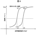
- FIG. 4 is a diagram illustrating drain current-reference electrode voltage characteristics.
- an interface potential is generated between the ion sensitive film 100 and the reagent solution 108, and the effective voltage applied to the gate electrode 103 changes. Since the magnitude of the interface potential depends on the ion concentration, for example, when the ion concentration of the solution 108 changes from C1 to C2, it seems that the transistor threshold value of the ISFET 114 changes from V1 to V2. From this change in threshold value, the ion concentration of the solution 108 can be measured.
- FIG. 5 is a functional block diagram of the biomolecule measuring apparatus according to the first embodiment.
- the biomolecule 115 to be measured is attached to the beads 702 and loaded onto the ISFET array 304.
- Reagents necessary for the ion reaction of the biomolecule 115 are delivered from the reagent container 301 by the liquid delivery device 303 and react with the biomolecule 115 on the ISFET array chip 1002.
- the ISFET array chip 1002 detects changes in the concentration of ions generated by this reaction.
- the waste liquid after the reaction is collected by a waste liquid container 310.
- the liquid feeding device 303 can be realized by using a plurality of common liquid feeding pumps, for example.
- an inert gas such as nitrogen or argon is injected into the reagent container 301 while adjusting the pressure via a valve prepared for each reagent container 301, and the reagent is pushed out of the reagent container 301 by the gas pressure. It can also be realized.
- the controller 312 adjusts the liquid feeding timing and the liquid feeding amount of the liquid feeding pump of the liquid feeding device 303 and the operation state of the ISFET array chip 1002 according to the pre-programmed experiment sequence and the data acquired by the data processing device 311. Control, control of the data processing device 311, voltage control of a reference electrode provided on any of the reagent flow paths 302, 313, and 314 or the ISFET chip 1002 are performed. Furthermore, the controller 312 controls the heater 308 similarly provided on the ISFET array chip 1002 and the cooling device 300 for cooling the reagent solution based on the measurement value of the temperature sensor 307 provided on the ISFET array chip 1002.
- the data processing device 311 acquires and analyzes data indicating the measurement result output from the ISFET array chip 1002.
- the data processing device 311 can be configured by an interface board equipped with a general A / D converter and a computer.
- the selection circuit 305 and the reading circuit 309 will be described later.
- FIG. 6 is a diagram for explaining the structure of DNA and the elongation reaction.
- FIG. 6A is a diagram schematically showing single-stranded DNA.
- four bases bind to a chain composed of phosphate and deoxyribose to form a complex three-dimensional structure, but here, for simplicity, the chain composed of phosphate and deoxyribose is linear. It is represented by 404, and four types of bases, that is, adenine is represented by A (400), thymine is represented by T (401), cytosine is represented by C (402), and guanine is represented by symbols such as G (403).
- FIG. 6B is a diagram schematically showing a DNA elongation reaction.
- a state where a primer 406 made of TAG is bound to a single strand 405 of ATCG is shown.
- dNTP deoxyribonucleotide triphosphate
- dCTP cytosine
- DNA polymerase which is an extension enzyme not shown in the figure
- a method for determining a DNA sequence by detecting hydrogen ions 408 is as follows. First, a primer 406 is bound to an unknown single-stranded DNA 405 whose sequence is to be determined. In this state, four types of reagents, dCTP, dTTP, dATP, and dGTP, are sequentially injected, and the hydrogen ion concentration when each reagent is injected is measured. For example, if hydrogen ions are generated when dATP is injected, it can be seen that the beginning of the original single-stranded DNA 405 excluding the portion to which the primer 406 is bound is the complementary base of A, that is, T. By repeating the reagent injection and the hydrogen ion concentration measurement, the DNA sequence can be determined in order.
- FIG. 7 is a flowchart for explaining a process in which the biomolecule measuring apparatus according to the first embodiment determines a DNA sequence. Hereinafter, each step of FIG. 7 will be described.
- Steps S600 to S601 When the beads 702 are completely loaded in the cell, the ISFET array chip 1002 is set in the apparatus. The reagent dNTP and the washing solution used for the reaction are cooled in advance using a cooling device 300 to a temperature sufficiently lower than the optimum temperature of the DNA polymerase.
- the controller 312 selects the reagent dNTP by a predetermined procedure (S600), and the liquid delivery device 303 injects the reagent solution 108 into the cell on the ISFET array chip 1002 (S601). At this stage, since the temperature of dNTP is low and the DNA polymerase hardly works, the extension reaction hardly occurs.
- Steps S602 to S604 The controller 312 activates the DNA polymerase by heating the well 703 and the reagent solution 108 in the well 703 using the heater 308 on the chip as a trigger for inducing an extension reaction (S602).
- the ISFET 114 measures the extension signal induced by the operation of the heater 308 (S603).
- the controller 312 injects a low-temperature cleaning solution by the liquid feeding device 303 to wash away unreacted dNTP and reaction product hydrogen ions and diphosphate, and at the same time, the cooling device The chip is cooled by 300 (S604).
- Steps S605 to S609 After the cleaning is completed, the controller 312 selects the next dNTP (S605 to S609), returns to step S601, and repeats the same processing.
- the expanded signal measured by the ISFET 114 in the process of repetition is converted into a digital signal by an A / D converter provided in the data processing device 311 and accumulated as measurement data in a storage device provided in the data processing device 311.
- the data processor 311 can specify the DNA structure according to the sequence obtained as a result of the repetition.
- FIG. 8 is a side view schematically showing one cell, and shows that the DNA 115 is fixed on the ISFET 114.
- the structure from the ion sensitive film 100 of the ISFET 114 to the gate electrode 103 is collectively shown by a rectangle 704.
- Washed away the hydrogen ion is a component or a reaction product of a dNTP solution is injected cleaning liquid in the cell at time T 604 followed is filled with washing liquid, returning to the same state as the time T 0. Moreover, by injecting the cleaning solution, the ISFET 114 is cooled to a low temperature lower than the optimum temperature of the DNA polymerase.
- FIG. 9 is a circuit diagram showing a configuration example of the ISFET array 304, the selection circuit 305, and the readout circuit 309 in the ISFET array chip 1002.
- the selection circuit 305 is configured by a general n-bit decoder and driver, and activates one of 2 ⁇ n row selection lines WL based on n row addresses given from the controller 312.
- the ISFET array 304 is a two-dimensional array of selection transistors for selecting the ISFET 114 and the ISFET 114 at the intersection of the row selection line WL and the data line DLA.
- Each cell 2303 includes two selection transistors 1200 and 1201 and an ISFET 114.
- Each cell is connected to a row selection line WLk, a source line SLk, and data lines DLAk, DLBk.
- the selection transistors are turned on in all the cells connected to the WLj, and all the ISFETs 114 on the same WLj are respectively connected to the source line SL and the data line. Connected to DLA.
- FIG. 9 shows an example in which all transistors are NMOSs, of course, all of them may be composed of PMOSs. In this case, the logic of the row selection line WL is inverted.
- the source line SLk, the data lines DLAk, and DLBk are connected to the k-th amplifier 2302-k in the read circuit 309.
- This amplifier comprises two general constant current sources 1700 and 1704, two amplifiers 1701 and 1702, and an output amplifier 1703 and a transistor 1705. Next, the operation of each amplifier when reading the signal from the ISFET 114 will be described.
- Constant current sources 1700 and 1703 draw a constant current to ground.
- the amplifiers 1701 and 1702 are amplifiers having a voltage follower configuration with an amplification factor of 1, and can be realized by a general differential amplifier circuit. These amplifiers generate a constant voltage VAB determined by the transistor 1705 and the constant current Id flowing through the constant current source 1704 between DLAk and DLBk. According to such a configuration, the source / drain voltage Vds of the selected ISFET in the ISFET array is fixed at a substantially constant value VAB, and the drain current is fixed at a constant current Id determined by the constant current source 1700.
- the drain current Id, the gate-source voltage Vgs, and the source-drain voltage Vds satisfy the following formula 1.
- ⁇ is a constant peculiar to ISFET 114
- Vth is a transistor threshold value of ISFET 114.
- Id ⁇ ⁇ (Vgs ⁇ Vth) ⁇ 1 / 2 ⁇ Vds ⁇ ⁇ Vds (Formula 1)
- Id ⁇ ⁇ (Vgs ′ ⁇ (Vth + ⁇ Vth)) ⁇ 1 ⁇ 2 ⁇ Vds ⁇ ⁇ Vds (Formula 2)
- Equation 3 if the gate voltage, that is, the voltage of the reference electrode 109 is fixed, the threshold fluctuation of the ISFET 114 is output as the fluctuation of the source potential. Since Vds is constant, the change in the source potential becomes the change in the drain potential, and as a result, ⁇ Vth is output from the amplifier output terminal Ok. However, since offset and background are superimposed on ⁇ Vth, as shown in FIG. 10 described later, the decompressed signal and these noises are temporally separated by the flowchart of FIG. 7, and only the decompressed signal is read accurately. Plan.
- one of the plurality of ISFETs 114 is selected by the selection circuit 305 and the output is read by the read circuit 309.
- An output pin may be provided for each ISFET 114.
- an A / D converter may be mounted on the ISFET array chip 1002, and the output of the ISFET 114 may be converted into digital data before being output. In this case, since the communication path from the ISFET array chip 1002 to the data processing device 311 is digitized, resistance to interference noise on the path is improved.
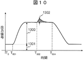
- FIG. 10 is a signal waveform obtained by reading the threshold fluctuation of one ISFET 114 when the flowchart of FIG. 7 is implemented by the circuit of FIG.
- a signal in which the waveform component 1301 and the background component 1300 resulting from drift and offset are superimposed is output from the ISFET 114.
- the rate of change of signal gradually decreases and approaches a certain value.
- the reagent solution 108 is heated by the heater 308 to activate the DNA polymerase.
- a trigger is generated so that the change in the background component 1300 and the extension signal are generated. 1302 can be separated in time.
- the expansion does not include these noises.
- a signal waveform can be easily obtained.
- the background estimation process using a plurality of empty wells described in Patent Document 2 is not necessary, and the process can be greatly reduced. Further, since the subtraction process is performed using the measured value of the ISFET 114 itself that measures the expansion signal 1302, it is not affected by the characteristic variation of the ISFET 114.
- the cell is cooled using the cleaning solution and dNTP, and the cell is heated using the heater 308 on the chip to induce the extension reaction.
- the method for controlling the temperature is not limited to this. Absent.
- a cooling mechanism such as a Peltier device may be brought into contact with the ISFET array chip 1002 to cool the chip.
- a generally used heater may be brought into contact with the ISFET array chip 1002 to heat the chip.
- FIG. 11 is a cross-sectional view of an ISFET array 304 on which heater wiring is mounted by a semiconductor process. Since the structure below the ion sensitive film 100 is the same as that shown in FIG. A wiring 900 is formed between the columns of the wells 703 by a semiconductor process, and a current is passed to generate Joule heat to heat the cells. According to this configuration, since the heat source is in the vicinity of the well 703, the temperature in the well 703 can be increased at high speed.
- the temperature of the reagent solution 108 after heating is close to the optimum temperature at which the DNA polymerase works most effectively.
- the optimum temperature greatly depends on the type of DNA polymerase. For example, when the DNA polymerase is Klenow Fragment, the temperature is around 37 ° C., and when it is Taq DNA polymerase, the temperature is 70 to 75 ° C. Further, if the temperature is too high, the enzyme may be denatured and deactivated, so it is necessary to prevent overheating. Therefore, a current is passed through the wiring 900 for a predetermined time to heat it, or a temperature sensor 307 is provided on the ISFET array chip 1002, and the heater 308 is monitored while monitoring the temperature so as to be close to the optimum temperature. It is good to control.
- the DNA elongation reaction is induced by heating from a low temperature to the optimal temperature of the DNA polymerase.
- the elongation reaction is induced by cooling from a temperature higher than the optimal temperature to the optimal temperature. Also good.
- Trigger for inducing elongation reaction is not limited to temperature.
- the photoresponsive nucleotide described in JP2009-126789A is used as the reagent solution 108
- UV irradiation with a wavelength of 366 nm can be used as an extension reaction trigger.
- the UV light source having a wavelength of 366 nm for example, a commercially available LED can be used.
- the reagent solution 108 may be divided into a buffer solution that does not induce an extension reaction and a dNTP reagent, and the dNTP reagent may be injected after the cell is first filled with the buffer solution. In this case, injection of dNTP reagent acts as a trigger.
- the function unit that generates a trigger for inducing an elongation reaction corresponds to a “trigger generation unit”.
- the timing T 602 for inducing the extension reaction can be determined as follows.
- One method is to measure the time T SAT from the time when the dNTP solution is injected until the change in the background signal becomes sufficiently small by experiment, and trigger the extension reaction when T SAT has elapsed from T 601.
- the controller 312 is programmed so that it can be applied.
- the background signal waveform is observed and the time when the change is stopped is automatically detected. This will be described with reference to FIG.
- FIG. 12 is a diagram showing the change over time of the background signal waveform and its differential value.
- Controller 312 differentiates the background signal waveform, may be employed time falls below the threshold value is preset as T 602. In this case, the extension reaction is started immediately when the amount of change in the background signal falls below the target value, and the time required for the measurement flow can be shortened.
- the differentiation of the signal waveform can be realized by a general differentiation circuit composed of an inverting amplifier, a capacitive element, and a resistance element.
- the threshold determination can be performed by a general voltage comparison circuit. Alternatively, waveform differentiation and threshold determination can be performed by software on the data processing device 311.
- FIG. 13 is a diagram showing a configuration example when the background is removed using a part of the ISFETs 114 on the ISFET array chip 1002. It is not always necessary to detect the background using all the ISFETs 114, and the background can also be detected using only the ISFETs 114 arranged on the downstream side in the direction in which the reagent solution 108 flows.
- T 602 may be determined based on a background waveform of one or more ISFETs 114 located closer to the reagent outlet 1104 than the reagent inlet 1103, that is, downstream of the solution flow. This is because if the change in the background waveform is settled on the downstream side, it can be determined that the solution exchange of the entire ISFET array chip 1002 has been completed. As shown in FIG. 13A, it is assumed that the dNTP solution 1101 is inserted from the reagent inlet 1103 and the cleaning liquid 1102 and dNTP solution are discharged from the reagent outlet 1104 to the cell filled with the cleaning liquid 1102.
- T 602 may be determined based on a background waveform of one or more ISFETs 114 located closer to the reagent outlet 1104 than the reagent inlet 1103, that is, downstream of the solution flow. This is because if the change in the background waveform is settled on the downstream side, it can be determined that the solution exchange of the entire ISFET array chip 1002 has been completed. As
- a dedicated cell 1105 for measuring the background may be provided downstream of the ISFET array chip 1002.
- a circuit for reading the background from the cell 1105 is preferably provided separately from the reading circuit 309.
- FIG. 14 is a circuit diagram including a read circuit 1106 for reading a signal output from the cell 1105 shown in FIG.
- the read circuit 1106 is a dedicated circuit independent of the read circuit 309.
- Other circuit configurations are the same as those in FIG.
- the circuit configuration shown in FIG. 14 eliminates the need to operate the selection circuit 305 of the ISFET array and the readout circuit 309 composed of a large number of constant current sources when measuring the background, thereby further reducing power consumption. it can.
- the reagent solution is heated by the heater 308 or other means after the liquid feeding device 303 starts sending the reagent solution 108, preferably after the delivery is finished. Generate a trigger to react 108.
- the decompressed signal 1302 and the background are separated in time, and only the decompressed signal 1302 can be easily extracted.
- the biomolecule measuring apparatus includes a circuit that fixes the drain current of the ISFET 114 to Id and fixes the source / drain voltage Vds to VAB. Thereby, as shown in Expression 3, only the threshold change ⁇ Vth of the ISFET 114 can be taken out from the output terminal Ok.
- the biomolecule measuring apparatus can subtract the drift / offset component 1301 and the background component 1300 detected by each ISFET 114 using only the signal output by each ISFET 114. Thereby, the amount of calculation for detecting a background can be suppressed. Furthermore, since the range of the data value is narrowed by suppressing the offset range, the conversion accuracy and data amount of the A / D converter can be suppressed.
- FIG. 15 is a circuit diagram excerpting one cell and its peripheral circuit on the ISFET array chip 1002 included in the biomolecule measuring device according to the second embodiment. Although not shown, there are actually a plurality of row selection lines WL, source lines SL, and data lines DLA and DLB as in FIG. For the ISFET 114, only the ion sensitive film 100 and the floating gate 102 are schematically shown, and the protective film 101 is omitted.
- the floating gate 102 is connected to a constant voltage source (for example, ground) via the transistor 1500.
- This constant voltage source fixes the potential of the gate input 102 of the ISFET 114, and does not necessarily have to be ground.
- the transistor 1500 is controlled by the drive signal ⁇ generated by the controller 312 and turns on / off the connection between the floating gate 102 and the constant voltage source.
- Other configurations are the same as those of the first embodiment.
- FIG. 16 is a flowchart for explaining a process in which the biomolecule measuring apparatus according to the second embodiment determines a DNA sequence. Hereinafter, each step of FIG. 16 will be described.
- Steps S1600 to S1601 These steps are the same as steps S600 to S601 in FIG. After step S1601, a background 1300 and a drift / offset component 1301 are detected as shown in FIG.
- Step S1602 The controller 312 applies a Hi signal as the drive signal ⁇ for the transistor 1500.
- the transistor 1500 When the transistor 1500 is turned on, the potential of the floating gate 102 is fixed to the ground. As a result, the background 1300 and the drift / offset component 1301 are reset. After these noises are reset, the controller 312 returns the transistor 1500 to OFF.
- the signal waveform detected by the ISFET 114 in this step is shown again in FIG.
- Steps S1603 to S1610 These steps are the same as steps S602 to S609 in FIG. After step S1610, the process returns to step S1601 and the same processing is repeated.
- FIG. 17 is a signal waveform obtained by reading the threshold fluctuation of one ISFET 114 when the flowchart of FIG. 16 is implemented by the circuit of FIG.
- ISFET114 detects background 1300 and the drift offset component 1301.
- the controller 312 performs step S1602 at time T 1602
- signal ISFET114 detects is reset to the signal reference point 1303. It is desirable that the time when the transistor 1500 is turned on is between the time when the background 1300 is stabilized and the time when the extension reaction trigger is supplied.
- the output signal of the ISFET 114 does not include the drift / offset component 1301 and the background component 1300, but only the expanded signal 1302. This eliminates the need for the data processing device 311 to perform the process of subtracting these noises, and can further reduce the processing load.
- the peak value of the signal output from the ISFET array chip 1002 can be kept low, the dynamic range required by the A / D converter can be reduced. Furthermore, since the amount of data is reduced, a data storage area can be saved.
- FIG. 17B shows a modification of the drive signal ⁇ .
- the drive signal ⁇ may be set to Hi when the dNTP solution is injected and washed, and the drive signal ⁇ may be set to Lo only when the extension signal 1302 is measured.
- the output value of the ISFET 114 is fixed at the signal reference point 1303 except when the expanded signal 1302 is measured, and a steep signal change can be eliminated, so that noise can be further reduced.
- the transistor 1500 is OFF when the extension signal 1302 is acquired.
- the transistor 1500 is driven before reaching the optimum temperature.
- the signal ⁇ may be Lo.
- the drive signal ⁇ may be set to Lo after the UV irradiation is completed for a certain time. Thereby, it is possible to reduce the influence that the output of the ISFET 114 is modulated by the high energy light of the UV light source.
- the biomolecule measuring apparatus includes the transistor 1500 that turns on / off the connection between the floating gate 102 and the constant voltage source, and the transistor 1500 is measured before the extension signal 1302 is measured. Turn on to reset noise. Thereby, the process of subtracting the noise component becomes unnecessary, and the calculation load of the data processing device 311 can be reduced. In addition, the dynamic range and data amount of the A / D converter can be kept small.
- the extension reaction trigger is output after the noise is reset using the transistor 1500 and the extension signal 1302 is measured.
- the transistor 1500 is used.
- the drift / offset component 1301 can be canceled.
- the temperature sensor 307, the heater 308, and the cooling device 300 are not necessary, and the system configuration can be simplified.
- the driving procedure of the biomolecule measuring apparatus is the same as that shown in FIG. 16 except for step S1603.
- FIG. 18 is a functional block diagram of the biomolecule measuring apparatus according to the third embodiment.
- the biomolecule measuring apparatus according to the third embodiment includes an excess solution removing apparatus 315 in addition to the configuration described in the second embodiment. Since the other configuration is the same as that of the second embodiment, the following description will focus on the differences.
- the surplus solution removing device 315 is a device that removes the reagent solution existing outside the well 703, and is controlled by the controller 312.
- the surplus solution removing device 315 can be configured by, for example, a pump for feeding a medium 1107 described later with reference to FIG. 19 into the cell.
- the medium 1107 is supplied via the reagent solution channel 316.
- FIG. 19 is a side sectional view of the well 703.
- the operation of the excess solution removing device 315 will be described with reference to FIG.
- the liquid feeding device 303 injects the dNTP solution 1101 from the reagent inlet 1103 into the cell filled with the cleaning liquid 1102, and discharges the cleaning liquid 1102 from the reagent outlet 1104.
- the surplus solution removing device 315 injects the medium 1107 into the cell from the reagent inlet 1103 and discharges the excess dNTP solution 1101 outside the well 703 from the reagent outlet 1104.
- the heater 308 heats the cell under the state shown in FIG. 19C, hydrogen ions 408 are generated.
- FIG. 20 is a flowchart for explaining a process in which the biomolecule measuring apparatus according to the third embodiment determines a DNA sequence. Hereinafter, each step of FIG. 20 will be described.
- Step S1900 to S1902 These steps are the same as steps S1600 to S1602 in FIG. However, in consideration of the points returned from steps S1910 to S1913, step S1901 for setting the drive signal ⁇ to Hi is performed first. In step S1902, since the transistor 1500 is ON, the drift / offset component 1301 and the background component 1300 are reset.
- the controller 312 drives the surplus solution removing device 315 to discharge the surplus dNTP solution 1101 outside the well 703 from the reagent discharge port 1104 as shown in FIG.
- a medium 1107 that is not mixed with the dNTP solution 1101 and has a lighter specific gravity than the dNTP solution 1101.
- air, an inert gas such as nitrogen or argon, and oil are suitable.
- Steps S1904 to S1913 These steps are the same as steps S1603 to S1610 in FIG. However, in this flowchart, since the drive signal ⁇ is set to Hi in step S1901 outside the loop, the drive signal ⁇ is set to Lo in steps S1904 and S1907 before and after the extension reaction trigger in order to match with this. It was decided to switch to Hi.
- the surplus solution removing device 315 separates the wells 703 while the DNA elongation reaction takes place, so that the hydrogen ions 408 can be prevented from propagating between the wells 703. That is, crosstalk between adjacent wells can be prevented. Further, since the dNTP solution 1101 exists only in the well 703, the generated hydrogen ions 408 diffuse out of the well 703 or disappear due to the buffer effect of the solution outside the well 703. Can be prevented from decaying. As a result, it is possible to expect an effect of increasing the peak value of the expanded signal 1302 and improving the duration of the signal.
- each well 703 is separated by removing the excess dNTP solution 1101, the conduction state between the reference electrode 109 and the dNTP solution 1101 in the well 703 may deteriorate.
- the reference electrode 109 may be provided individually in the well 703.
- the substrate surface of the ISFET array chip 1002 may be coated with a material having water repellency with respect to the dNTP solution 1101.
- the water repellency of the coating material is sufficient if it can promote the removal of excess dNTP solution 1101.
- it is possible to impart water repellency with commercially available fluorine-based coating agents such as Teflon (registered trademark, DuPont) and Cytop (registered trademark, Asahi Glass).
- Teflon registered trademark, DuPont
- Cytop registered trademark, Asahi Glass
- FIG. 21 is a diagram showing another configuration example for separating the wells 703.
- each well 703 instead of removing the excess dNTP solution 1101 with the medium 1107, each well 703 is covered with a structure 1108. Thereby, each well 703 can be separated without adding the medium 1107.
- FIG. 22 is a diagram showing the internal structure of the structure 1108. As shown in FIG. 22, the solution in the well 703 can be heated more quickly by adding a heater 1110 on the structure 1108 side. Further, a reference electrode 1109 may be provided on the structure 1108 side and connected to another circuit portion through wirings 1111 and 1112. Further, the surface of the structure 1108 may be coated with a material having water repellency with respect to the dNTP solution 1101. Thereby, the possibility that the excess dNTP solution 1101 remains on the substrate surface without being removed can be further reduced.
- the biomolecule measuring apparatus separates each well 703 and prevents signal components from interfering with each other between adjacent wells 703 due to crosstalk. As a result, the signal quality of the ISFET 114 can be improved.
- the present invention is not limited to the above-described embodiment, and includes various modifications.
- the above embodiment has been described in detail for easy understanding of the present invention, and is not necessarily limited to the one having all the configurations described.
- a part of the configuration of one embodiment can be replaced with the configuration of another embodiment.
- the configuration of another embodiment can be added to the configuration of a certain embodiment. Further, with respect to a part of the configuration of each embodiment, another configuration can be added, deleted, or replaced.
- Embodiments 1 to 3 an example of measuring the reaction of sample DNA immobilized on beads 702 has been shown.
- DNA is immobilized on well 703 whose surface is chemically modified. May be. This can reduce the possibility of the beads 702 and sample DNA being washed away when the solution is exchanged.
- the present invention is not limited to a measurement apparatus that specifies the structure of a DNA sample, but can be applied to a general measurement apparatus that detects ions generated by a reaction between a biomolecule sample and a reagent.
- a measurement apparatus that specifies the structure of a DNA sample
- a general measurement apparatus that detects ions generated by a reaction between a biomolecule sample and a reagent.
- an ISFET has been described as an example of a semiconductor sensor that detects ions, other semiconductor sensors may be used as long as they have the same function.
Abstract
Description
図1は、後述するISFETアレイ304の構成を示す図である。図1(a)は、ISFETアレイ304のなかの3つのISFET114と反応槽(以下、ウェルと呼ぶ)111~113の側断面図であり、図1(b)のA-A’線断面図に相当する。図1(b)は、ISFETアレイ304の上面図である。なお、各トランジスタへの配線は省略してある。 <Prior art issues: Measurement error>
FIG. 1 is a diagram showing a configuration of an
図1に示す通り、チップを製造した段階でISFET114の構造上に正電荷800や負電荷801がトラップされ、その量はISFET114ごとに異なり、これがISFET114内のトランジスタ閾値がオフセットする原因となる。トラップされる場所は、主にイオン感応膜100の表面、イオン感応膜100と保護膜101との間の界面、フローティングゲート102、ゲート酸化膜104である。各ISFET114のトランジスタ閾値は、トラップされた電荷の種類と量に依存してオフセットする。 <Prior art issues: data volume>
As shown in FIG. 1,
以下、図面を用いて本発明の実施形態を説明する。ここでは半導体センサとしてISFETを用い、生体分子計測装置としてDNAの配列を決定するDNAシーケンサを例として示すが、本発明の適用先はDNAシーケンサに限定されるものではなく、生体分子の反応生成物を電気的に計測するシステムに広く適用することができる。ISFETはイオン感応膜を適切に選択することによって種々のイオンを検出することができるので、例えばナトリウムイオンやカリウムイオンが変化するような生体分子を測定する装置に対して本発明を適用することができ。なお、実施形態を説明するための全図において、同一の部材には原則として同一の符号を付し、その繰り返しの説明は省略する。 <
Hereinafter, embodiments of the present invention will be described with reference to the drawings. Here, an ISFET is used as a semiconductor sensor, and a DNA sequencer that determines the DNA sequence as a biomolecule measuring device is shown as an example. Can be widely applied to systems that electrically measure the current. Since ISFET can detect various ions by appropriately selecting an ion sensitive membrane, for example, the present invention can be applied to a device that measures biomolecules in which sodium ions or potassium ions change. Yes. Note that components having the same function are denoted by the same reference symbols throughout the drawings for describing the embodiment, and the repetitive description thereof will be omitted.
ビーズ702をセルに装填し終えた段階でISFETアレイチップ1002を装置にセットする。反応に用いる試薬dNTPと洗浄液は、あらかじめ冷却装置300を用いて、DNAポリメラーゼの至適温度より十分低い温度に冷却しておく。測定を開始すると、コントローラ312はあらかじめ決められた手順で試薬dNTPを選択し(S600)、送液装置303は試薬溶液108をISFETアレイチップ1002上のセルに注入する(S601)。この段階では、dNTPの温度が低くDNAポリメラーゼがほとんど働かないため、伸長反応はほぼ起こらない。 (FIG. 7: Steps S600 to S601)
When the
コントローラ312は、伸長反応を誘起するトリガとして、チップ上のヒータ308を用いてウェル703とウェル703内の試薬溶液108を加熱し、DNAポリメラーゼを活性化させる(S602)。ISFET114は、ヒータ308の動作によって誘起された伸長信号を測定する(S603)。伸長信号を測定し終えた段階で、コントローラ312は送液装置303によって低温の洗浄液を注入し、反応しなかったdNTPと、反応生成物である水素イオン、2リン酸を洗い流すと同時に、冷却装置300によりチップを冷却する(S604)。 (FIG. 7: Steps S602 to S604)
The
コントローラ312は、洗浄が終わった後、次のdNTPを選択し(S605~S609)、ステップS601に戻って同様の処理を繰り返す。繰り返しの過程においてISFET114が測定した伸長信号は、データ処理装置311が備えるA/D変換器によってデジタル信号に変換され、データ処理装置311が備える記憶装置内に測定データとして蓄積される。データ処理装置311は、繰り返しの結果得られる配列にしたがって、DNAの構造を特定することができる。 (FIG. 7: Steps S605 to S609)
After the cleaning is completed, the
Id=β{(Vgs-Vth)-1/2×Vds}×Vds (式1) Constant
Id = β {(Vgs−Vth) −1 / 2 × Vds} × Vds (Formula 1)
Id=β{(Vgs’-(Vth+ΔVth))-1/2×Vds}×Vds (式2) Assuming that the threshold value of
Id = β {(Vgs ′ − (Vth + ΔVth)) − ½ × Vds} × Vds (Formula 2)
Vgs’-Vgs=ΔVth (式3) Since Id is not 0, the following formula 3 is obtained by dividing (formula 1) by (formula 2).
Vgs′−Vgs = ΔVth (Formula 3)
以上の説明においては、洗浄液とdNTPを用いてセルを冷却し、チップ上のヒータ308を用いてセルを加熱して伸長反応を誘起する例を示したが、温度を制御する手法はこれに限らない。例えば、ペルチェ素子などの冷却機構をISFETアレイチップ1002に接触させてチップを冷却してもよい。また、一般的に使われるヒータをISFETアレイチップ1002に接触させてチップを加熱してもよい。ただし、伸長反応を誘起する加熱に関しては、なるべく急峻に温度を変化させることが望ましい。なぜなら、温度が緩やかに上昇すると、ビーズ702上の複製DNAの伸長反応が同時に起こらず、伸長信号ピークがなだらかになるからである。 <Embodiment 1: Modification>
In the above description, the cell is cooled using the cleaning solution and dNTP, and the cell is heated using the
以上のように、本実施形態1に係る生体分子計測装置は、送液装置303が試薬溶液108を送出し始めた後、好適には送出し終えた後に、ヒータ308またはその他の手段によって試薬溶液108を反応させるトリガを生成する。これにより、図10に示すように伸長信号1302とバックグラウンドを時間的に分離し、伸長信号1302のみを容易に取り出すことができる。 <Embodiment 1: Summary>
As described above, in the biomolecule measuring apparatus according to the first embodiment, the reagent solution is heated by the
実施形態1においては、ISFET114が検出した信号波形からドリフト・オフセット成分1301とバックグラウンド1300を演算によって差し引き、伸長信号1302のみを取り出すことを説明した。本発明の実施形態2では、ドリフト・オフセット成分1301とバックグラウンド1300を差し引く別の構成例について説明する。 <
In the first embodiment, it has been described that the drift / offset
これらのステップは、図7におけるステップS600~S601と同様である。ステップS1601の後、後述する図17に示すようにバックグラウンド1300とドリフト・オフセット成分1301が検出される。 (FIG. 16: Steps S1600 to S1601)
These steps are the same as steps S600 to S601 in FIG. After step S1601, a
コントローラ312は、トランジスタ1500に対する駆動信号φとして、Hi信号を印加する。トランジスタ1500がONになると、フローティングゲート102の電位がグラウンドに固定される。これにより、バックグラウンド1300とドリフト・オフセット成分1301がリセットされる。コントローラ312は、これらノイズがリセットされた後、トランジスタ1500をOFFに戻す。本ステップにおいてISFET114が検出する信号波形は、後述の図17で改めて示す。 (FIG. 16: Step S1602)
The
これらのステップは、図7におけるステップS602~S609と同様である。ステップS1610の次は、ステップS1601に戻って同様の処理を繰り返す。 (FIG. 16: Steps S1603 to S1610)
These steps are the same as steps S602 to S609 in FIG. After step S1610, the process returns to step S1601 and the same processing is repeated.
以上のように、本実施形態2に係る生体分子計測装置は、フローティングゲート102と定電圧源との間の接続をON/OFFするトランジスタ1500を備え、伸長信号1302を測定する前にトランジスタ1500をONしてノイズをリセットする。これにより、ノイズ成分を差し引く処理が不要になり、データ処理装置311の演算負荷を軽減することができる。また、A/Dコンバータのダイナミックレンジやデータ量を小さく抑えることができる。 <Embodiment 2: Summary>
As described above, the biomolecule measuring apparatus according to the second embodiment includes the
実施形態1~2においては、ドリフト・オフセット成分1301とバックグラウンド成分1300を除去することによってISFET114の信号品質を改善する構成例について説明した。本発明の実施形態3では、他の手段によってISFET114の信号品質を改善する構成例について説明する。 <Embodiment 3>
In the first and second embodiments, the configuration example in which the signal quality of the
これらのステップは、図16におけるステップS1600~S1602と同様である。ただし、ステップS1910~S1913から戻ってくる箇所を考慮して、駆動信号φをHiにするステップS1901を先に実施することとした。ステップS1902においてはトランジスタ1500がONになっているため、ドリフト・オフセット成分1301とバックグラウンド成分1300はリセットされている。 (FIG. 20: Steps S1900 to S1902)
These steps are the same as steps S1600 to S1602 in FIG. However, in consideration of the points returned from steps S1910 to S1913, step S1901 for setting the drive signal φ to Hi is performed first. In step S1902, since the
コントローラ312は、余剰溶液除去装置315を駆動し、図19(b)に示すように、ウェル703外にある余剰なdNTP溶液1101を試薬排出口1104から排出する。ウェル703の中にのみdNTP溶液1101を残すためには、媒質1107はdNTP溶液1101と混ざらず、かつdNTP溶液1101より比重の軽いものを用いることが望ましい。例えば空気、窒素やアルゴンなどの不活性ガス、油が好適である。 (FIG. 20: Step S1903)
The
これらのステップは、図16のステップS1603~S1610と同様である。ただし本フローチャートにおいては、ループ外のステップS1901で駆動信号φをHiにセットしているので、これと整合を取るため、伸長反応トリガの前後であるステップS1904とS1907においてそれぞれ駆動信号φをLoとHiに切り替えることとした。 (FIG. 20: Steps S1904 to S1913)
These steps are the same as steps S1603 to S1610 in FIG. However, in this flowchart, since the drive signal φ is set to Hi in step S1901 outside the loop, the drive signal φ is set to Lo in steps S1904 and S1907 before and after the extension reaction trigger in order to match with this. It was decided to switch to Hi.
図21は、各ウェル703を分離する別構成例を示す図である。図21において、媒質1107によって余剰なdNTP溶液1101を除去することに代えて、構造物1108を用いて各ウェル703に蓋をする。これにより、媒質1107を追加することなく各ウェル703を分離することができる。 <Embodiment 3: Modification>
FIG. 21 is a diagram showing another configuration example for separating the
以上のように、本実施形態3に係る生体分子計測装置は、各ウェル703を分離し、隣接するウェル703間でクロストークにより信号成分が干渉することを防ぐ。これによりISFET114の信号品質を向上させることができる。 <Embodiment 3: Summary>
As described above, the biomolecule measuring apparatus according to the third embodiment separates each well 703 and prevents signal components from interfering with each other between
101 保護膜
102 フローティングゲート
103 ゲート電極
104 ゲート酸化膜
105 ドレイン
106 ソース
107 シリコン基板
108 試薬溶液
109、1109 参照電極
110 基板コンタクト
111、112、113、703 ウェル
114 ISFET
115 DNA
116 セル
300 冷却装置
301 試薬容器
302、313、314、316 試薬溶液流路
303 送液装置
304 ISFETアレイ
305 選択回路
307 温度センサ
308、1110 ヒータ
309 読み出し回路
310 廃液容器
311 データ処理装置
312 コントローラ
315 余剰溶液除去装置
1002 ISFETアレイチップ
1003、1701、1702、2302 アンプ
1101 dNTP溶液
1102 洗浄液
1103 試薬注入口
1104 試薬排出口
1105 バックグラウンド測定用セル
1106 読み出し回路
1107 媒質
1108 構造物
1111、1112 配線
1200、1201 選択トランジスタ
1300 バックグラウンド成分
1301 ドリフト・オフセット成分
1302 伸長反応に由来する成分
1303 信号基準点
1500 トランジスタ
1700、1703、1704 定電流源
1705 トランジスタ
2303 セル
DLA、DLA1、DLAk、DLB、DLB1、DLBk データ線
O1、O2、Ok アンプ出力端子
SL、SL1、SL2、SLk ソース線 100 Ion
115 DNA
116
Claims (15)
- 生体分子試料と化学反応してイオンを生成させる試薬を送出する送液装置と、
前記イオンの濃度を測定する半導体センサと、
前記化学反応を誘起する物理環境を生じさせるトリガ生成部と、
前記送液装置と前記トリガ生成部の動作を制御するコントローラと、
前記半導体センサの測定結果に基づき前記生体分子試料の構成を特定する処理装置と、
を備え、
前記コントローラは、
前記送液装置が前記半導体センサ上に配置された前記生体分子試料上に前記試薬を送出し始めた後に、前記トリガ生成部が前記物理環境を生じさせるように、前記送液装置と前記トリガ生成部を制御する
ことを特徴とする生体分子計測装置。 A liquid delivery device that delivers a reagent that chemically reacts with a biomolecule sample to generate ions;
A semiconductor sensor for measuring the concentration of the ions;
A trigger generating unit for generating a physical environment for inducing the chemical reaction;
A controller for controlling the operation of the liquid feeding device and the trigger generation unit;
A processing device for identifying the configuration of the biomolecule sample based on the measurement result of the semiconductor sensor;
With
The controller is
The liquid supply device and the trigger generation so that the trigger generation unit generates the physical environment after the liquid supply device starts to deliver the reagent onto the biomolecule sample disposed on the semiconductor sensor. The biomolecule measuring device characterized by controlling a part. - 前記コントローラは、
前記送液装置が前記試薬を送出し終えた後に、前記トリガ生成部が前記物理環境を生じさせるように、前記送液装置と前記トリガ生成部を制御し、
複数種類の前記試薬を入れ替えながら前記試薬を送出する動作と前記物理環境を生じさせる動作を、前記送液装置と前記トリガ生成部に繰り返し実施させ、
前記処理装置は、
前記繰り返しの過程において得られる前記半導体センサの各測定結果に基づき、前記生体分子試料の構成を特定する
ことを特徴とする請求項1記載の生体分子計測装置。 The controller is
After the liquid delivery device has finished delivering the reagent, the liquid delivery device and the trigger generation unit are controlled so that the trigger generation unit generates the physical environment,
The liquid feeding device and the trigger generating unit repeatedly perform the operation of sending out the reagent while exchanging a plurality of types of the reagent and the operation of generating the physical environment,
The processor is
The biomolecule measuring device according to claim 1, wherein the configuration of the biomolecule sample is specified based on each measurement result of the semiconductor sensor obtained in the repetition process. - 前記半導体センサは、前記測定結果を電気信号として出力するドレイン端子を有するトランジスタを備え、
前記生体分子計測装置は、前記トランジスタのドレイン電流と前記トランジスタのソース-ドレイン間電圧をそれぞれ一定に維持する回路を備え、
前記処理装置は、前記送液装置が前記試薬を送出し終えてから前記トリガ生成部が前記物理環境を生じさせるまでにおける前記測定結果を、前記トリガ生成部が前記物理環境を生じさせた以降における前記測定結果から差し引く差分演算を実施することにより、前記試薬に起因して生じるノイズを前記測定結果から除去する
ことを特徴とする請求項2記載の生体分子計測装置。 The semiconductor sensor includes a transistor having a drain terminal that outputs the measurement result as an electrical signal,
The biomolecule measuring device includes a circuit that maintains the drain current of the transistor and the source-drain voltage of the transistor constant,
The processing apparatus is configured to display the measurement result from when the liquid delivery device finishes delivering the reagent until the trigger generation unit generates the physical environment, after the trigger generation unit generates the physical environment. The biomolecule measuring device according to claim 2, wherein noise generated due to the reagent is removed from the measurement result by performing a difference calculation to be subtracted from the measurement result. - 前記生体分子計測装置は、アレイ状に配置された複数の前記半導体センサを備え、
前記処理装置は、各前記半導体センサの前記測定結果のみを前記半導体センサ毎にそれぞれ用いることにより、前記半導体センサ毎に前記差分演算を実施する
ことを特徴とする請求項3記載の生体分子計測装置。 The biomolecule measuring device comprises a plurality of the semiconductor sensors arranged in an array,
The biomolecule measuring device according to claim 3, wherein the processing device performs the difference calculation for each of the semiconductor sensors by using only the measurement result of each of the semiconductor sensors for each of the semiconductor sensors. . - 前記生体分子計測装置は、前記送液装置が前記試薬を送出する方向の上流側と下流側にそれぞれ配置された前記半導体センサを備え、
前記回路は、前記下流側に配置された前記半導体センサが備える前記トランジスタのドレイン電流とソース-ドレイン間電圧をそれぞれ一定に維持し、
前記処理装置は、前記下流側に配置された前記半導体センサの測定結果を用いて、前記試薬に起因して生じるノイズを各前記半導体センサの測定結果から除去する
ことを特徴とする請求項3記載の生体分子計測装置。 The biomolecule measuring device includes the semiconductor sensors respectively disposed on the upstream side and the downstream side in the direction in which the liquid feeding device delivers the reagent,
The circuit maintains a constant drain current and a source-drain voltage of the transistor included in the semiconductor sensor disposed on the downstream side,
The said processing apparatus removes the noise which originates in the said reagent from the measurement result of each said semiconductor sensor using the measurement result of the said semiconductor sensor arrange | positioned in the said downstream. Biomolecule measuring device. - 前記処理装置は、前記半導体センサの測定結果の時間微分を計算し、
前記コントローラは、前記時間微分の計算値が所定閾値以下になった時点で、前記トリガ生成部が前記物理環境を生じさせるように、前記トリガ生成部を制御する
ことを特徴とする請求項2記載の生体分子計測装置。 The processing device calculates a time derivative of the measurement result of the semiconductor sensor,
The said controller controls the said trigger production | generation part so that the said trigger production | generation part produces the said physical environment, when the calculated value of the said time differentiation becomes below a predetermined threshold value. Biomolecule measuring device. - 前記トリガ生成部は、前記試薬の温度を制御するか、または紫外線を前記試薬に照射することにより、前記物理環境を生じさせる
ことを特徴とする請求項1記載の生体分子計測装置。 The biomolecule measuring device according to claim 1, wherein the trigger generation unit generates the physical environment by controlling the temperature of the reagent or irradiating the reagent with ultraviolet rays. - 前記送液装置は、前記化学反応を生じないバッファ溶液を送出した後、前記化学反応を生じさせる試薬を送出する
ことを特徴とする請求項1記載の生体分子計測装置。 The biomolecule measuring device according to claim 1, wherein the liquid delivery device delivers a reagent that causes the chemical reaction after delivering a buffer solution that does not cause the chemical reaction. - 前記半導体センサは、
前記測定結果を電気信号として出力するドレイン端子を有するトランジスタを備え、
前記生体分子計測装置は、
前記トランジスタのゲート電極に固定電圧を提供する電圧源と、
前記電圧源と前記トランジスタのゲート電極との間の接続をON/OFF切替するスイッチング素子と、
を備え、
前記コントローラは、
前記スイッチング素子をONして前記電圧源と前記トランジスタのゲート電極の間を接続した後に、前記トリガ生成部に前記物理環境を生成させ、
前記処理装置は、
前記試薬に起因して生じるノイズを前記測定結果から除去することなく、前記生体分子試料の構成を特定する
ことを特徴とする請求項2記載の生体分子計測装置。 The semiconductor sensor is
A transistor having a drain terminal for outputting the measurement result as an electrical signal;
The biomolecule measuring device is
A voltage source for providing a fixed voltage to the gate electrode of the transistor;
A switching element for switching ON / OFF the connection between the voltage source and the gate electrode of the transistor;
With
The controller is
After turning on the switching element and connecting between the voltage source and the gate electrode of the transistor, the trigger generation unit generates the physical environment,
The processor is
The biomolecule measuring device according to claim 2, wherein the configuration of the biomolecule sample is specified without removing noise caused by the reagent from the measurement result. - 前記生体分子計測装置は、前記試薬を収容する凹部を備え、
前記半導体センサは、前記凹部の底部に接続されており、
前記生体分子計測装置はさらに、前記凹部の外に存在する余分な前記試薬を除去する除去装置を備える
ことを特徴とする請求項2記載の生体分子計測装置。 The biomolecule measuring device includes a recess for storing the reagent,
The semiconductor sensor is connected to the bottom of the recess,
The biomolecule measuring apparatus according to claim 2, further comprising a removing device that removes the extra reagent existing outside the concave portion. - 前記生体分子計測装置は、前記試薬を収容する凹部を備え、
前記半導体センサは、前記凹部の底部に接続されており、
前記生体分子計測装置はさらに、前記凹部の外に存在する余分な前記試薬を除去する除去装置を備え、
前記コントローラは、
前記除去装置が余分な前記試薬を除去した後に、前記スイッチング素子をOFFして前記電圧源と前記トランジスタのゲート電極の間を切断し、さらにその後に前記トリガ生成部に前記物理環境を生成させる
ことを特徴とする請求項9記載の生体分子計測装置。 The biomolecule measuring device includes a recess for storing the reagent,
The semiconductor sensor is connected to the bottom of the recess,
The biomolecule measuring device further includes a removing device for removing the excess reagent existing outside the concave portion,
The controller is
After the removal device removes the excess reagent, the switching element is turned off to disconnect between the voltage source and the gate electrode of the transistor, and then the trigger generation unit generates the physical environment. The biomolecule measuring device according to claim 9. - 前記生体分子計測装置は、前記凹部が形成された基板を備え、
前記基板の表面は、前記試薬に対して撥水性を有する材料によって被覆されている
ことを特徴とする請求項10記載の生体分子計測装置。 The biomolecule measuring device includes a substrate on which the concave portion is formed,
The biomolecule measuring device according to claim 10, wherein the surface of the substrate is coated with a material having water repellency with respect to the reagent. - 前記生体分子計測装置は、前記試薬を収容する凹部を備え、
前記半導体センサは、前記凹部の底部に接続されており、
前記生体分子計測装置はさらに、前記凹部を封止する蓋部を備える
ことを特徴とする請求項2記載の生体分子計測装置。 The biomolecule measuring device includes a recess for storing the reagent,
The semiconductor sensor is connected to the bottom of the recess,
The biomolecule measuring device according to claim 2, further comprising a lid portion that seals the concave portion. - 前記トリガ生成部は、前記蓋部に取り付けられており、前記凹部内に収容されている前記試薬に前記化学反応を誘起させるように、前記物理環境を生じさせる
ことを特徴とする請求項13記載の生体分子計測装置。 The said trigger production | generation part is attached to the said cover part, The said physical environment is produced so that the said chemical reaction may be induced in the said reagent accommodated in the said recessed part. Biomolecule measuring device. - 前記半導体センサは、
前記イオンによって界面電位が変動するイオン感応膜と、
前記界面電位の変動によって生じる電気信号を前記測定結果として出力するトランジスタと、
を備えるイオン感応トランジスタとして構成されている
ことを特徴とする請求項1記載の生体分子計測装置。 The semiconductor sensor is
An ion-sensitive membrane whose interface potential varies with the ions;
A transistor that outputs an electrical signal generated by the fluctuation of the interface potential as the measurement result;
The biomolecule measuring device according to claim 1, wherein the device is configured as an ion sensitive transistor.
Priority Applications (4)
| Application Number | Priority Date | Filing Date | Title |
|---|---|---|---|
| EP13871321.9A EP2947453B1 (en) | 2013-01-17 | 2013-11-18 | Biomolecule measuring device |
| CN201380069342.2A CN104884948B (en) | 2013-01-17 | 2013-11-18 | Biomolecule measurement apparatus |
| US14/759,596 US10451584B2 (en) | 2013-01-17 | 2013-11-18 | Biomolecule measuring device |
| JP2014557340A JP6030153B2 (en) | 2013-01-17 | 2013-11-18 | Biomolecule measuring device |
Applications Claiming Priority (2)
| Application Number | Priority Date | Filing Date | Title |
|---|---|---|---|
| JP2013-006391 | 2013-01-17 | ||
| JP2013006391 | 2013-01-17 |
Publications (1)
| Publication Number | Publication Date |
|---|---|
| WO2014112199A1 true WO2014112199A1 (en) | 2014-07-24 |
Family
ID=51209311
Family Applications (1)
| Application Number | Title | Priority Date | Filing Date |
|---|---|---|---|
| PCT/JP2013/081014 WO2014112199A1 (en) | 2013-01-17 | 2013-11-18 | Biomolecule measuring device |
Country Status (5)
| Country | Link |
|---|---|
| US (1) | US10451584B2 (en) |
| EP (1) | EP2947453B1 (en) |
| JP (1) | JP6030153B2 (en) |
| CN (1) | CN104884948B (en) |
| WO (1) | WO2014112199A1 (en) |
Cited By (9)
| Publication number | Priority date | Publication date | Assignee | Title |
|---|---|---|---|---|
| EP3268496A4 (en) * | 2015-03-09 | 2018-09-05 | Agilome, Inc. | Graphene fet devices, systems, and methods of using the same for sequencing nucleic acids |
| US10429342B2 (en) | 2014-12-18 | 2019-10-01 | Edico Genome Corporation | Chemically-sensitive field effect transistor |
| US10429381B2 (en) | 2014-12-18 | 2019-10-01 | Agilome, Inc. | Chemically-sensitive field effect transistors, systems, and methods for manufacturing and using the same |
| US10494670B2 (en) | 2014-12-18 | 2019-12-03 | Agilome, Inc. | Graphene FET devices, systems, and methods of using the same for sequencing nucleic acids |
| US10607989B2 (en) | 2014-12-18 | 2020-03-31 | Nanomedical Diagnostics, Inc. | Graphene FET devices, systems, and methods of using the same for sequencing nucleic acids |
| US10811539B2 (en) | 2016-05-16 | 2020-10-20 | Nanomedical Diagnostics, Inc. | Graphene FET devices, systems, and methods of using the same for sequencing nucleic acids |
| JP2022500055A (en) * | 2018-09-13 | 2022-01-04 | 連 俊龍Chun−Lung LIEN | Nucleotide sequencing devices, chips and methods of sequencing analysis |
| US11782057B2 (en) | 2014-12-18 | 2023-10-10 | Cardea Bio, Inc. | Ic with graphene fet sensor array patterned in layers above circuitry formed in a silicon based cmos wafer |
| US11921112B2 (en) | 2014-12-18 | 2024-03-05 | Paragraf Usa Inc. | Chemically-sensitive field effect transistors, systems, and methods for manufacturing and using the same |
Families Citing this family (5)
| Publication number | Priority date | Publication date | Assignee | Title |
|---|---|---|---|---|
| US10768173B1 (en) * | 2019-09-06 | 2020-09-08 | Element Biosciences, Inc. | Multivalent binding composition for nucleic acid analysis |
| US11293897B2 (en) * | 2018-11-30 | 2022-04-05 | Taiwan Semiconductor Manufacturing Company, Ltd. | High sensitivity ISFET sensor |
| CN109652287B (en) * | 2019-01-03 | 2021-04-30 | 京东方科技集团股份有限公司 | Micro-control substrate, manufacturing method thereof and micro-fluidic chip |
| CN110358681A (en) * | 2019-07-09 | 2019-10-22 | 成都万众壹芯生物科技有限公司 | A kind of portable PCR device |
| US11287422B2 (en) | 2019-09-23 | 2022-03-29 | Element Biosciences, Inc. | Multivalent binding composition for nucleic acid analysis |
Citations (7)
| Publication number | Priority date | Publication date | Assignee | Title |
|---|---|---|---|---|
| JP2009126789A (en) | 2007-11-19 | 2009-06-11 | Japan Advanced Institute Of Science & Technology Hokuriku | Photo-responding base having triazole skeleton |
| JP2010513869A (en) | 2006-12-14 | 2010-04-30 | イオン トーレント システムズ インコーポレーテッド | Method and apparatus for analyte measurement using large-scale FET arrays |
| JP2010519914A (en) * | 2007-03-02 | 2010-06-10 | ディ・エヌ・エイ・エレクトロニクス・リミテッド | QPCR using solid phase pH detection |
| WO2012027391A1 (en) * | 2010-08-23 | 2012-03-01 | Life Technologies Corporation | Temperature control of chemical detection system |
| JP2012506557A (en) * | 2008-10-22 | 2012-03-15 | ライフ テクノロジーズ コーポレーション | Integrated sensor arrays for biological and chemical analysis |
| US20120172241A1 (en) | 2010-12-30 | 2012-07-05 | Life Technologies Corporation | Models for analyzing data from sequencing-by-synthesis operations |
| JP2012528329A (en) * | 2009-05-29 | 2012-11-12 | ライフ テクノロジーズ コーポレーション | Apparatus and method for conducting electrochemical reactions |
Family Cites Families (13)
| Publication number | Priority date | Publication date | Assignee | Title |
|---|---|---|---|---|
| AU2907092A (en) * | 1991-10-21 | 1993-05-21 | James W. Holm-Kennedy | Method and device for biochemical sensing |
| GB0105831D0 (en) | 2001-03-09 | 2001-04-25 | Toumaz Technology Ltd | Method for dna sequencing utilising enzyme linked field effect transistors |
| WO2003052097A1 (en) * | 2001-12-19 | 2003-06-26 | Hitachi High-Technologies Corporation | Potentiometric dna microarray, process for producing the same and method of analyzing nucleic acid |
| JP3903183B2 (en) * | 2004-02-03 | 2007-04-11 | 独立行政法人物質・材料研究機構 | Gene detection field effect device and gene polymorphism analysis method using the same |
| US8349167B2 (en) * | 2006-12-14 | 2013-01-08 | Life Technologies Corporation | Methods and apparatus for detecting molecular interactions using FET arrays |
| US8262900B2 (en) * | 2006-12-14 | 2012-09-11 | Life Technologies Corporation | Methods and apparatus for measuring analytes using large scale FET arrays |
| EP2251435B1 (en) * | 2007-03-02 | 2013-10-16 | DNA Electronics Ltd | Sensing apparatus for monitoring nucleic acid amplification, using an ion-sensitive field effect transistor (ISFET) for pH sensing |
| WO2009006445A2 (en) * | 2007-06-29 | 2009-01-08 | Applied Biosystems | Systems and methods for electronic detection with nanofets |
| GB2461026B (en) | 2008-06-16 | 2011-03-09 | Plc Diagnostics Inc | System and method for nucleic acids sequencing by phased synthesis |
| US20100301398A1 (en) | 2009-05-29 | 2010-12-02 | Ion Torrent Systems Incorporated | Methods and apparatus for measuring analytes |
| US20100137143A1 (en) * | 2008-10-22 | 2010-06-03 | Ion Torrent Systems Incorporated | Methods and apparatus for measuring analytes |
| GB2483402B (en) * | 2009-06-04 | 2014-04-09 | Lockheed Corp | Multiple-sample microfluidic chip for DNA analysis |
| US10241075B2 (en) * | 2010-12-30 | 2019-03-26 | Life Technologies Corporation | Methods, systems, and computer readable media for nucleic acid sequencing |
-
2013
- 2013-11-18 WO PCT/JP2013/081014 patent/WO2014112199A1/en active Application Filing
- 2013-11-18 EP EP13871321.9A patent/EP2947453B1/en active Active
- 2013-11-18 JP JP2014557340A patent/JP6030153B2/en active Active
- 2013-11-18 CN CN201380069342.2A patent/CN104884948B/en active Active
- 2013-11-18 US US14/759,596 patent/US10451584B2/en active Active
Patent Citations (7)
| Publication number | Priority date | Publication date | Assignee | Title |
|---|---|---|---|---|
| JP2010513869A (en) | 2006-12-14 | 2010-04-30 | イオン トーレント システムズ インコーポレーテッド | Method and apparatus for analyte measurement using large-scale FET arrays |
| JP2010519914A (en) * | 2007-03-02 | 2010-06-10 | ディ・エヌ・エイ・エレクトロニクス・リミテッド | QPCR using solid phase pH detection |
| JP2009126789A (en) | 2007-11-19 | 2009-06-11 | Japan Advanced Institute Of Science & Technology Hokuriku | Photo-responding base having triazole skeleton |
| JP2012506557A (en) * | 2008-10-22 | 2012-03-15 | ライフ テクノロジーズ コーポレーション | Integrated sensor arrays for biological and chemical analysis |
| JP2012528329A (en) * | 2009-05-29 | 2012-11-12 | ライフ テクノロジーズ コーポレーション | Apparatus and method for conducting electrochemical reactions |
| WO2012027391A1 (en) * | 2010-08-23 | 2012-03-01 | Life Technologies Corporation | Temperature control of chemical detection system |
| US20120172241A1 (en) | 2010-12-30 | 2012-07-05 | Life Technologies Corporation | Models for analyzing data from sequencing-by-synthesis operations |
Non-Patent Citations (5)
| Title |
|---|
| GEORGIOU, ELECTRONICS LETT., October 2009 (2009-10-01) |
| HAMMOND, IEEE SENSORS, December 2004 (2004-12-01) |
| KERKHOF, SENSORS AND ACTUATORS B, 1994 |
| LIU, IEEE TRANS. ELEC. DEV, December 2011 (2011-12-01) |
| MILGREW, IEEE ELEC. DEV., April 2008 (2008-04-01) |
Cited By (12)
| Publication number | Priority date | Publication date | Assignee | Title |
|---|---|---|---|---|
| US10429342B2 (en) | 2014-12-18 | 2019-10-01 | Edico Genome Corporation | Chemically-sensitive field effect transistor |
| US10429381B2 (en) | 2014-12-18 | 2019-10-01 | Agilome, Inc. | Chemically-sensitive field effect transistors, systems, and methods for manufacturing and using the same |
| US10494670B2 (en) | 2014-12-18 | 2019-12-03 | Agilome, Inc. | Graphene FET devices, systems, and methods of using the same for sequencing nucleic acids |
| US10607989B2 (en) | 2014-12-18 | 2020-03-31 | Nanomedical Diagnostics, Inc. | Graphene FET devices, systems, and methods of using the same for sequencing nucleic acids |
| US11536722B2 (en) | 2014-12-18 | 2022-12-27 | Cardea Bio, Inc. | Chemically-sensitive field effect transistors, systems, and methods for manufacturing and using the same |
| US11732296B2 (en) | 2014-12-18 | 2023-08-22 | Cardea Bio, Inc. | Two-dimensional channel FET devices, systems, and methods of using the same for sequencing nucleic acids |
| US11782057B2 (en) | 2014-12-18 | 2023-10-10 | Cardea Bio, Inc. | Ic with graphene fet sensor array patterned in layers above circuitry formed in a silicon based cmos wafer |
| US11921112B2 (en) | 2014-12-18 | 2024-03-05 | Paragraf Usa Inc. | Chemically-sensitive field effect transistors, systems, and methods for manufacturing and using the same |
| EP3268496A4 (en) * | 2015-03-09 | 2018-09-05 | Agilome, Inc. | Graphene fet devices, systems, and methods of using the same for sequencing nucleic acids |
| US10811539B2 (en) | 2016-05-16 | 2020-10-20 | Nanomedical Diagnostics, Inc. | Graphene FET devices, systems, and methods of using the same for sequencing nucleic acids |
| JP2022500055A (en) * | 2018-09-13 | 2022-01-04 | 連 俊龍Chun−Lung LIEN | Nucleotide sequencing devices, chips and methods of sequencing analysis |
| JP7171901B2 (en) | 2018-09-13 | 2022-11-15 | 俊龍 連 | Nucleotide sequencing elements, chips and methods of sequencing analysis |
Also Published As
| Publication number | Publication date |
|---|---|
| CN104884948A (en) | 2015-09-02 |
| CN104884948B (en) | 2018-01-09 |
| EP2947453B1 (en) | 2018-09-05 |
| JP6030153B2 (en) | 2016-11-24 |
| EP2947453A1 (en) | 2015-11-25 |
| US10451584B2 (en) | 2019-10-22 |
| JPWO2014112199A1 (en) | 2017-01-19 |
| US20150362458A1 (en) | 2015-12-17 |
| EP2947453A4 (en) | 2016-08-24 |
Similar Documents
| Publication | Publication Date | Title |
|---|---|---|
| JP6030153B2 (en) | Biomolecule measuring device | |
| US20230101252A1 (en) | Apparatus and methods for performing electrochemical reactions | |
| JP4353958B2 (en) | DNA measuring apparatus and DNA measuring method | |
| JP2020073910A (en) | Ion-sensing charge-accumulation circuits and methods | |
| JP5932915B2 (en) | Integrated sensor arrays for biological and chemical analysis | |
| JP5913323B2 (en) | Matched pair transistor circuit | |
| TWI684004B (en) | Methods and apparatus for measuring analytes using large scale fet arrays | |
| EP2008717B1 (en) | Reaction device with accurate temperature control | |
| JP6247064B2 (en) | Biomolecule measuring device | |
| JP2014115125A (en) | Biological molecule measuring device, and biological molecule measuring method | |
| US20140243214A1 (en) | Fet array substrate, analysis system and method | |
| JP2004007572A (en) | Electronic apparatus, its drive method, and drive method for electronic circuit | |
| JP2015210233A (en) | Massively parallel biomolecule detection method and apparatus | |
| CN105593675B (en) | Biomolecule measuring device | |
| JP2007255906A (en) | Electrode type solution measuring method and electrode type solution measuring instrument | |
| TWI834132B (en) | Sensing chip with fluid device | |
| JP2009254258A (en) | Heat control matrix device and reaction treatment device | |
| TW202300907A (en) | Sensing chip with fluid device | |
| CN115508426A (en) | Sensing chip with fluidic device |
Legal Events
| Date | Code | Title | Description |
|---|---|---|---|
| 121 | Ep: the epo has been informed by wipo that ep was designated in this application |
Ref document number: 13871321 Country of ref document: EP Kind code of ref document: A1 |
|
| ENP | Entry into the national phase |
Ref document number: 2014557340 Country of ref document: JP Kind code of ref document: A |
|
| WWE | Wipo information: entry into national phase |
Ref document number: 2013871321 Country of ref document: EP |
|
| WWE | Wipo information: entry into national phase |
Ref document number: 14759596 Country of ref document: US |
|
| NENP | Non-entry into the national phase |
Ref country code: DE |