WO2013065245A1 - Non-contact wireless communication coil, transmission coil, and portable wireless terminal - Google Patents
Non-contact wireless communication coil, transmission coil, and portable wireless terminal Download PDFInfo
- Publication number
- WO2013065245A1 WO2013065245A1 PCT/JP2012/006644 JP2012006644W WO2013065245A1 WO 2013065245 A1 WO2013065245 A1 WO 2013065245A1 JP 2012006644 W JP2012006644 W JP 2012006644W WO 2013065245 A1 WO2013065245 A1 WO 2013065245A1
- Authority
- WO
- WIPO (PCT)
- Prior art keywords
- coil
- magnetic body
- wireless communication
- magnetic
- contact
- Prior art date
Links
- 238000004891 communication Methods 0.000 title claims abstract description 224
- 230000005540 biological transmission Effects 0.000 title claims abstract description 177
- 239000000758 substrate Substances 0.000 claims abstract description 64
- 230000035699 permeability Effects 0.000 claims abstract description 55
- 230000002093 peripheral effect Effects 0.000 claims description 39
- 230000001105 regulatory effect Effects 0.000 claims description 7
- 239000002184 metal Substances 0.000 claims description 4
- 229910052751 metal Inorganic materials 0.000 claims description 4
- 238000010586 diagram Methods 0.000 description 65
- 230000008878 coupling Effects 0.000 description 58
- 238000010168 coupling process Methods 0.000 description 58
- 238000005859 coupling reaction Methods 0.000 description 58
- 230000000052 comparative effect Effects 0.000 description 41
- 239000003990 capacitor Substances 0.000 description 30
- 230000015556 catabolic process Effects 0.000 description 27
- 238000006731 degradation reaction Methods 0.000 description 27
- 230000006866 deterioration Effects 0.000 description 25
- 125000006850 spacer group Chemical group 0.000 description 24
- 239000004020 conductor Substances 0.000 description 22
- 238000005259 measurement Methods 0.000 description 17
- 238000004804 winding Methods 0.000 description 11
- 230000007423 decrease Effects 0.000 description 9
- 239000000463 material Substances 0.000 description 8
- 238000011156 evaluation Methods 0.000 description 7
- 239000011521 glass Substances 0.000 description 7
- 229910000859 α-Fe Inorganic materials 0.000 description 6
- 239000004593 Epoxy Substances 0.000 description 5
- 238000000034 method Methods 0.000 description 5
- RYGMFSIKBFXOCR-UHFFFAOYSA-N Copper Chemical compound [Cu] RYGMFSIKBFXOCR-UHFFFAOYSA-N 0.000 description 4
- 238000004519 manufacturing process Methods 0.000 description 4
- 239000000203 mixture Substances 0.000 description 4
- 230000004048 modification Effects 0.000 description 4
- 238000012986 modification Methods 0.000 description 4
- 230000009467 reduction Effects 0.000 description 4
- XECAHXYUAAWDEL-UHFFFAOYSA-N acrylonitrile butadiene styrene Chemical compound C=CC=C.C=CC#N.C=CC1=CC=CC=C1 XECAHXYUAAWDEL-UHFFFAOYSA-N 0.000 description 3
- 229920000122 acrylonitrile butadiene styrene Polymers 0.000 description 3
- 239000004676 acrylonitrile butadiene styrene Substances 0.000 description 3
- 230000008859 change Effects 0.000 description 3
- 229910052802 copper Inorganic materials 0.000 description 3
- 239000010949 copper Substances 0.000 description 3
- 229920005989 resin Polymers 0.000 description 3
- 239000011347 resin Substances 0.000 description 3
- PPBRXRYQALVLMV-UHFFFAOYSA-N Styrene Chemical compound C=CC1=CC=CC=C1 PPBRXRYQALVLMV-UHFFFAOYSA-N 0.000 description 2
- 238000006073 displacement reaction Methods 0.000 description 2
- 239000003822 epoxy resin Substances 0.000 description 2
- 229920000647 polyepoxide Polymers 0.000 description 2
- 238000005452 bending Methods 0.000 description 1
- 239000000470 constituent Substances 0.000 description 1
- 239000011889 copper foil Substances 0.000 description 1
- 230000003247 decreasing effect Effects 0.000 description 1
- 230000000694 effects Effects 0.000 description 1
- 230000005674 electromagnetic induction Effects 0.000 description 1
- 238000009774 resonance method Methods 0.000 description 1
- 238000004088 simulation Methods 0.000 description 1
- 230000001629 suppression Effects 0.000 description 1
Images


Classifications
-
- H—ELECTRICITY
- H01—ELECTRIC ELEMENTS
- H01F—MAGNETS; INDUCTANCES; TRANSFORMERS; SELECTION OF MATERIALS FOR THEIR MAGNETIC PROPERTIES
- H01F38/00—Adaptations of transformers or inductances for specific applications or functions
- H01F38/14—Inductive couplings
-
- H—ELECTRICITY
- H01—ELECTRIC ELEMENTS
- H01Q—ANTENNAS, i.e. RADIO AERIALS
- H01Q1/00—Details of, or arrangements associated with, antennas
- H01Q1/12—Supports; Mounting means
- H01Q1/22—Supports; Mounting means by structural association with other equipment or articles
- H01Q1/2208—Supports; Mounting means by structural association with other equipment or articles associated with components used in interrogation type services, i.e. in systems for information exchange between an interrogator/reader and a tag/transponder, e.g. in Radio Frequency Identification [RFID] systems
- H01Q1/2225—Supports; Mounting means by structural association with other equipment or articles associated with components used in interrogation type services, i.e. in systems for information exchange between an interrogator/reader and a tag/transponder, e.g. in Radio Frequency Identification [RFID] systems used in active tags, i.e. provided with its own power source or in passive tags, i.e. deriving power from RF signal
-
- H—ELECTRICITY
- H01—ELECTRIC ELEMENTS
- H01Q—ANTENNAS, i.e. RADIO AERIALS
- H01Q1/00—Details of, or arrangements associated with, antennas
- H01Q1/12—Supports; Mounting means
- H01Q1/22—Supports; Mounting means by structural association with other equipment or articles
- H01Q1/24—Supports; Mounting means by structural association with other equipment or articles with receiving set
- H01Q1/241—Supports; Mounting means by structural association with other equipment or articles with receiving set used in mobile communications, e.g. GSM
- H01Q1/242—Supports; Mounting means by structural association with other equipment or articles with receiving set used in mobile communications, e.g. GSM specially adapted for hand-held use
- H01Q1/243—Supports; Mounting means by structural association with other equipment or articles with receiving set used in mobile communications, e.g. GSM specially adapted for hand-held use with built-in antennas
-
- H—ELECTRICITY
- H01—ELECTRIC ELEMENTS
- H01Q—ANTENNAS, i.e. RADIO AERIALS
- H01Q1/00—Details of, or arrangements associated with, antennas
- H01Q1/12—Supports; Mounting means
- H01Q1/22—Supports; Mounting means by structural association with other equipment or articles
- H01Q1/24—Supports; Mounting means by structural association with other equipment or articles with receiving set
- H01Q1/248—Supports; Mounting means by structural association with other equipment or articles with receiving set provided with an AC/DC converting device, e.g. rectennas
-
- H—ELECTRICITY
- H01—ELECTRIC ELEMENTS
- H01Q—ANTENNAS, i.e. RADIO AERIALS
- H01Q1/00—Details of, or arrangements associated with, antennas
- H01Q1/36—Structural form of radiating elements, e.g. cone, spiral, umbrella; Particular materials used therewith
- H01Q1/38—Structural form of radiating elements, e.g. cone, spiral, umbrella; Particular materials used therewith formed by a conductive layer on an insulating support
-
- H—ELECTRICITY
- H01—ELECTRIC ELEMENTS
- H01Q—ANTENNAS, i.e. RADIO AERIALS
- H01Q1/00—Details of, or arrangements associated with, antennas
- H01Q1/52—Means for reducing coupling between antennas; Means for reducing coupling between an antenna and another structure
- H01Q1/521—Means for reducing coupling between antennas; Means for reducing coupling between an antenna and another structure reducing the coupling between adjacent antennas
-
- H—ELECTRICITY
- H01—ELECTRIC ELEMENTS
- H01Q—ANTENNAS, i.e. RADIO AERIALS
- H01Q21/00—Antenna arrays or systems
- H01Q21/28—Combinations of substantially independent non-interacting antenna units or systems
-
- H—ELECTRICITY
- H01—ELECTRIC ELEMENTS
- H01Q—ANTENNAS, i.e. RADIO AERIALS
- H01Q5/00—Arrangements for simultaneous operation of antennas on two or more different wavebands, e.g. dual-band or multi-band arrangements
- H01Q5/40—Imbricated or interleaved structures; Combined or electromagnetically coupled arrangements, e.g. comprising two or more non-connected fed radiating elements
-
- H—ELECTRICITY
- H01—ELECTRIC ELEMENTS
- H01Q—ANTENNAS, i.e. RADIO AERIALS
- H01Q7/00—Loop antennas with a substantially uniform current distribution around the loop and having a directional radiation pattern in a plane perpendicular to the plane of the loop
-
- H—ELECTRICITY
- H01—ELECTRIC ELEMENTS
- H01Q—ANTENNAS, i.e. RADIO AERIALS
- H01Q7/00—Loop antennas with a substantially uniform current distribution around the loop and having a directional radiation pattern in a plane perpendicular to the plane of the loop
- H01Q7/06—Loop antennas with a substantially uniform current distribution around the loop and having a directional radiation pattern in a plane perpendicular to the plane of the loop with core of ferromagnetic material
-
- H—ELECTRICITY
- H02—GENERATION; CONVERSION OR DISTRIBUTION OF ELECTRIC POWER
- H02J—CIRCUIT ARRANGEMENTS OR SYSTEMS FOR SUPPLYING OR DISTRIBUTING ELECTRIC POWER; SYSTEMS FOR STORING ELECTRIC ENERGY
- H02J50/00—Circuit arrangements or systems for wireless supply or distribution of electric power
- H02J50/005—Mechanical details of housing or structure aiming to accommodate the power transfer means, e.g. mechanical integration of coils, antennas or transducers into emitting or receiving devices
-
- H—ELECTRICITY
- H02—GENERATION; CONVERSION OR DISTRIBUTION OF ELECTRIC POWER
- H02J—CIRCUIT ARRANGEMENTS OR SYSTEMS FOR SUPPLYING OR DISTRIBUTING ELECTRIC POWER; SYSTEMS FOR STORING ELECTRIC ENERGY
- H02J50/00—Circuit arrangements or systems for wireless supply or distribution of electric power
- H02J50/10—Circuit arrangements or systems for wireless supply or distribution of electric power using inductive coupling
- H02J50/12—Circuit arrangements or systems for wireless supply or distribution of electric power using inductive coupling of the resonant type
-
- H—ELECTRICITY
- H02—GENERATION; CONVERSION OR DISTRIBUTION OF ELECTRIC POWER
- H02J—CIRCUIT ARRANGEMENTS OR SYSTEMS FOR SUPPLYING OR DISTRIBUTING ELECTRIC POWER; SYSTEMS FOR STORING ELECTRIC ENERGY
- H02J50/00—Circuit arrangements or systems for wireless supply or distribution of electric power
- H02J50/20—Circuit arrangements or systems for wireless supply or distribution of electric power using microwaves or radio frequency waves
-
- H—ELECTRICITY
- H02—GENERATION; CONVERSION OR DISTRIBUTION OF ELECTRIC POWER
- H02J—CIRCUIT ARRANGEMENTS OR SYSTEMS FOR SUPPLYING OR DISTRIBUTING ELECTRIC POWER; SYSTEMS FOR STORING ELECTRIC ENERGY
- H02J50/00—Circuit arrangements or systems for wireless supply or distribution of electric power
- H02J50/70—Circuit arrangements or systems for wireless supply or distribution of electric power involving the reduction of electric, magnetic or electromagnetic leakage fields
-
- H—ELECTRICITY
- H02—GENERATION; CONVERSION OR DISTRIBUTION OF ELECTRIC POWER
- H02J—CIRCUIT ARRANGEMENTS OR SYSTEMS FOR SUPPLYING OR DISTRIBUTING ELECTRIC POWER; SYSTEMS FOR STORING ELECTRIC ENERGY
- H02J50/00—Circuit arrangements or systems for wireless supply or distribution of electric power
- H02J50/80—Circuit arrangements or systems for wireless supply or distribution of electric power involving the exchange of data, concerning supply or distribution of electric power, between transmitting devices and receiving devices
-
- H—ELECTRICITY
- H02—GENERATION; CONVERSION OR DISTRIBUTION OF ELECTRIC POWER
- H02J—CIRCUIT ARRANGEMENTS OR SYSTEMS FOR SUPPLYING OR DISTRIBUTING ELECTRIC POWER; SYSTEMS FOR STORING ELECTRIC ENERGY
- H02J7/00—Circuit arrangements for charging or depolarising batteries or for supplying loads from batteries
- H02J7/00032—Circuit arrangements for charging or depolarising batteries or for supplying loads from batteries characterised by data exchange
- H02J7/00034—Charger exchanging data with an electronic device, i.e. telephone, whose internal battery is under charge
-
- H—ELECTRICITY
- H04—ELECTRIC COMMUNICATION TECHNIQUE
- H04B—TRANSMISSION
- H04B5/00—Near-field transmission systems, e.g. inductive or capacitive transmission systems
- H04B5/20—Near-field transmission systems, e.g. inductive or capacitive transmission systems characterised by the transmission technique; characterised by the transmission medium
- H04B5/24—Inductive coupling
- H04B5/26—Inductive coupling using coils
- H04B5/263—Multiple coils at either side
-
- H—ELECTRICITY
- H04—ELECTRIC COMMUNICATION TECHNIQUE
- H04B—TRANSMISSION
- H04B5/00—Near-field transmission systems, e.g. inductive or capacitive transmission systems
- H04B5/40—Near-field transmission systems, e.g. inductive or capacitive transmission systems characterised by components specially adapted for near-field transmission
- H04B5/48—Transceivers
-
- H—ELECTRICITY
- H04—ELECTRIC COMMUNICATION TECHNIQUE
- H04B—TRANSMISSION
- H04B5/00—Near-field transmission systems, e.g. inductive or capacitive transmission systems
- H04B5/70—Near-field transmission systems, e.g. inductive or capacitive transmission systems specially adapted for specific purposes
- H04B5/72—Near-field transmission systems, e.g. inductive or capacitive transmission systems specially adapted for specific purposes for local intradevice communication
-
- H—ELECTRICITY
- H04—ELECTRIC COMMUNICATION TECHNIQUE
- H04B—TRANSMISSION
- H04B5/00—Near-field transmission systems, e.g. inductive or capacitive transmission systems
- H04B5/70—Near-field transmission systems, e.g. inductive or capacitive transmission systems specially adapted for specific purposes
- H04B5/79—Near-field transmission systems, e.g. inductive or capacitive transmission systems specially adapted for specific purposes for data transfer in combination with power transfer
Definitions
- the present invention relates to a coil for contactless wireless communication capable of contactless power transmission and contactless wireless communication, and a portable wireless terminal equipped with the coil.
- portable wireless terminals such as mobile phone terminals and smartphones are widely equipped with non-contact wireless communication (so-called RFID (Radio Frequency Identification)) such as NFC (Near Field Communication) including FeliCa (registered trademark).
- RFID Radio Frequency Identification
- NFC Near Field Communication
- FeliCa registered trademark
- Non-contact power transmission methods include an electromagnetic induction method, a magnetic field resonance method, and the like, and a method that performs power transmission with a coil on a power feeding side and a coil on a power receiving side facing each other is the mainstream.
- a charging coil integrated with a battery pack is the mainstream. For this reason, when it is going to make a battery pack thin for further thickness reduction of a terminal, there exists a big subject that battery capacity decreases. On the other hand, when the charging coil is configured separately from the battery pack, coexistence with the non-contact wireless communication coil becomes a problem in the portable wireless terminal equipped with the above-described non-contact wireless communication function.
- the contactless wireless communication coil and the contactless power transmission coil coexist.
- a first coil that forms a power wave antenna and a second coil that forms a data wave antenna form a double ring.
- An arranged wireless card is disclosed. With this configuration, the first coil and the second coil are less likely to be covered with fingers of a hand holding the wireless card, and the reception status of both coils can be made substantially the same.
- the present invention has been made in view of the above circumstances, and its purpose is to suppress the performance deterioration of each coil when a plurality of coils such as a non-contact wireless communication coil and a non-contact power transmission coil coexist. However, it is to be realized in a space-saving manner.
- the present invention includes a first coil, a second coil, a first magnetic body, and a second magnetic body, and in the thickness direction of the coil, the first magnetic body, the first coil, and the second magnetic body.
- a contactless wireless communication coil is provided in which the body and the second coil are stacked in this order and at least a part of the first coil and the second coil overlap each other.
- the present invention includes the above-described coil for non-contact wireless communication, wherein the magnetic permeability of the first magnetic body is higher than the magnetic permeability of the second magnetic body.
- the present invention also includes the above-described contactless wireless communication coil, wherein the resonance frequency of the first coil is lower than the resonance frequency of the second coil.
- the present invention includes the above-described non-contact wireless communication coil in which at least a part of the second coil is overlapped near the outer periphery of the first coil.
- the present invention includes the above-described non-contact wireless communication coil in which at least a part of the second coil is located outside the first coil.
- the present invention includes the above-mentioned contactless wireless communication coil, wherein the first coil is for contactless power transmission and the second coil is for contactless wireless communication.
- the present invention provides a portable wireless terminal equipped with any one of the above-described non-contact wireless communication coils.
- the present invention is a transmission coil, which is a first coil, a second coil, a first magnetic body having a predetermined permeability, and a second having a permeability different from the predetermined permeability of the first magnetic body.
- a magnetic body, and in the thickness direction of the coil the first coil is disposed on the surface of the first magnetic body, and the second coil is disposed on the surface of the second magnetic body.
- the second magnetic body is disposed on the outer periphery of the first magnetic body, the first boundary surface between the first coil and the first magnetic body, the second coil, and the second magnetic body.
- the second boundary surface is substantially the same plane, or the second boundary surface is an upper portion in the thickness direction of the coil than the first boundary surface.
- the present invention is the above transmission coil, wherein the first boundary surface and the second boundary surface are substantially the same plane, or the second boundary surface is in the thickness direction of the coil from the first boundary surface.
- the thickness of the second magnetic body is set with respect to the thickness of the first magnetic body so as to be an upper part.
- this invention is said transmission coil, Comprising:
- the said 2nd magnetic body in the thickness direction of the said coil is provided in the surface on the opposite side to the surface where the said 2nd coil is arrange
- a position regulating member that regulates the position of the first boundary surface and the second boundary surface are substantially flush with each other, or the second boundary surface is above the first boundary surface in the thickness direction of the coil.
- the present invention includes the transmission coil described above, wherein the magnetic permeability of the first magnetic body is higher than the magnetic permeability of the second magnetic body.
- the present invention includes the transmission coil described above, wherein the resonance frequency of the first coil is lower than the resonance frequency of the second coil.
- the present invention includes the transmission coil described above, wherein the first coil is for non-contact power transmission and the second coil is for non-contact wireless communication.
- the present invention is a portable wireless terminal equipped with any one of the above transmission coils.
- the present invention is a transmission coil, which is a first coil, a second coil, a first magnetic body having a predetermined permeability, and a second having a permeability different from the predetermined permeability of the first magnetic body.
- a magnetic body wherein the first coil is disposed on a surface of the first magnetic body, and the second magnetic body is disposed on a surface of the first magnetic body and outside the first coil.
- the second coil is disposed on the surface of the second magnetic body.
- the present invention includes the transmission coil described above, wherein the magnetic permeability of the first magnetic body is higher than the magnetic permeability of the second magnetic body.
- the present invention includes the transmission coil described above, wherein the resonance frequency of the first coil is lower than the resonance frequency of the second coil.
- the present invention further includes a guide portion that is the above-described transmission coil and guides the distance between the first coil and the second coil to be equal to or greater than a predetermined interval.
- the present invention includes the transmission coil described above, wherein the guide portion is formed on a peripheral portion of the second magnetic body on the first coil side.
- the present invention further includes a transmission coil as described above, wherein the transmission coil is further disposed on the outside of the first coil, and the second coil is formed as a predetermined metal pattern. And formed on the peripheral edge of the substrate on the first coil side.
- the present invention includes the transmission coil described above, wherein the first coil is for non-contact power transmission and the second coil is for non-contact wireless communication.
- the present invention is a portable wireless terminal equipped with any one of the above transmission coils.
- the present invention when a plurality of coils such as a non-contact wireless communication coil and a non-contact power transmission coil coexist, it can be realized in a space-saving manner while suppressing performance deterioration of each coil. .
- the thickness of the housing is reduced while suppressing performance deterioration of each coil. Can be realized easily.
- the present invention when a plurality of coils such as a non-contact wireless communication coil and a non-contact power transmission coil coexist, it is possible to easily manufacture in a space-saving manner while suppressing performance deterioration of each coil. Can do.
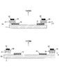
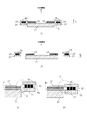
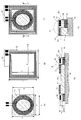
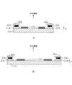
- FIG. 1A is a cross-sectional view taken along the line AA ′ in FIG. 1
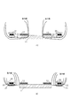
- FIG. (A) and (B) are diagrams showing the magnetic field distribution of the coil unit at the position of the cross section along the line AA ′ of FIG. 1 (position of FIG. 2 (A)).
- (A) and (B) are diagrams showing the magnetic field distribution of the coil unit at the position of the cross section along the line BB ′ of FIG. 1 (position of FIG. 2 (B)).
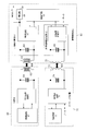
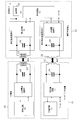
- FIG. 1 is a block diagram showing a configuration of a portable wireless terminal equipped with a coil unit of the present embodiment, a charger as an external device, and a reader / writer device.
- (A)-(D) are figures which show the dimension of the coil unit of the Example based on this invention.
- (A), (B) is a figure which shows the result of having measured the power transmission efficiency at the time of non-contact power transmission, and the maximum communication distance at the time of non-contact wireless communication as a performance of the coil unit of the Example which concerns on this invention.
- 8A and 8B are diagrams illustrating a configuration of a coil unit according to a second embodiment of the present invention, in which FIG. 8A is a plan view of the coil unit, FIG.
- FIG. 8B is a cross-sectional view taken along line AA ′ in FIG. ) Is a cross-sectional view taken along the line BB ′ of FIG. 9A and 9B are diagrams illustrating a configuration of a coil unit according to a third embodiment of the present invention, in which FIG. 9A is a plan view of the coil unit, FIG. 9B is a cross-sectional view taken along line AA ′ in FIG. ) Is a cross-sectional view taken along line BB ′ of FIG. (A) and (B) are modifications in which the inner diameter and the outer shape of the first coil and the second coil are the same.
- (A) to (E) are modifications in which the arrangement of both coils is changed when the first coil is an elliptical ring and the second coil is a square ring.
- (A) to (E) are modified examples in which the arrangement of the two coils is changed when the first coil is a square round ring and the second coil is a square ring.
- It is a figure which shows the structure of the coil unit of a comparative example (A) is a top view of a coil unit, (B) is the sectional view on the AA 'line of FIG. 13 (A). A top view showing composition of a coil unit concerning a 4th embodiment. Sectional view of coil unit of fourth embodiment, (A) sectional view taken along line AA 'in FIG.
- FIG. 15 (A) A diagram showing the magnetic field distribution of the coil unit during the operation of the first coil at the position of the cross section along line AA ′ of FIG. 14 (position of FIG. 15A), (B) AA of FIG. The figure which shows the magnetic field distribution of the coil unit at the time of operation
- FIG. 15B 15B
- 1 is a block diagram showing a configuration of a portable wireless terminal equipped with a coil unit of the present embodiment, a charger as an external device, and a reader / writer device.
- FIG. 19C The figure explaining the change of the communication performance of the 2nd coil 22 when the position of the 2nd magnetic body 21 varies in the thickness direction of a coil
- (D) the position of the second magnetic body 21 is the thickness of the coil.
- the figure which shows the comparison result of each communication performance of the 2nd coil 22 in the state which varies in the direction where communication performance becomes high in the direction, and the state where communication performance becomes low The figure which shows the structure of the coil unit which concerns on 6th Embodiment, (A) The top view which shows the structure of a coil unit, (B) And (C) Sectional drawing in the AA 'line of FIG. 26 (A) The figure which shows the structure of the coil unit which concerns on Example 1 at the time of arrange
- FIG. 7 is a diagram showing an example of dimensions, (C) a plan view of the coil unit according to the first embodiment, (D) a cross-sectional view taken along the line AA ′ in FIG. 27 (C), and (E) a region g in FIG. Enlarged view of The figure which shows the structure of the coil unit which concerns on Example 2 in case the thickness of 21 C of 2nd magnetic bodies is substantially equal to the thickness of the 1st magnetic body 11, (A) and (B) The dimension of the coil unit which concerns on Example 2 (C) A plan view of the coil unit according to the second embodiment, (D) a sectional view taken along the line AA ′ in FIG. 28 (C), (E) an area h in FIG. 28 (D).
- FIG. 32A A diagram showing the magnetic field distribution of the coil unit during the operation of the first coil at the position of the cross section along line AA ′ of FIG. 31 (position of FIG. 32A), (B) AA of FIG. 'A diagram showing the magnetic field distribution of the coil unit at the time of operation of the second coil at the position of the cross section (position of FIG. 32A).
- FIG. 1 is a block diagram showing a configuration of a portable wireless terminal equipped with a coil unit of the present embodiment, a charger as an external device, and a reader / writer device.
- A The figure which shows an example of the dimension of the coil unit which concerns on an Example
- C The top view of the coil unit which concerns on an Example
- D The cross section in the AA 'line of FIG.36
- Figure (A) The figure which shows the result of having measured the power transmission efficiency at the time of non-contact power transmission as performance of the coil unit which concerns on an Example,
- (B) The maximum at the time of non-contact wireless communication as performance of the coil unit which concerns on an Example The figure which shows the result of measuring the communication distance
- A The figure which shows an example of the dimension of the coil unit which concerns on a comparative example
- C The top view of the coil unit which concerns on a comparative example
- D The cross section in the AA 'line of FIG
- FIG. 40 (A) Cross-sectional view taken along line AA ′ in FIG. 40, (B) Cross-sectional view taken along line BB ′ in FIG. The figure explaining the space
- FIG. 1 Figure (A) Table showing measurement results under conditions a and b, (B) Graph showing measurement results under conditions a and b (A)-(C) Cross-sectional view explaining the flow of assembly of the coil unit
- C Plan view of the coil unit according to Embodiment 1
- D Sectional view taken along the line AA ′ in FIG.
- FIGS. 19A and 19B are diagrams showing other examples of the shapes of various guide members.
- a coil unit having a contactless wireless communication coil and a contactless power transmission coil, and the coil unit are mounted.
- wireless terminal is shown.
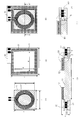
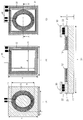
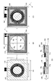
- FIG. 1 is a plan view showing the configuration of the coil unit according to the first embodiment of the present invention.
- 2 is a cross-sectional view of the coil unit according to the first embodiment.
- FIG. 2A is a cross-sectional view taken along the line AA ′ in FIG. 1
- FIG. 2B is a cross-sectional view taken along the line BB ′ in FIG. It is.
- the coil unit of the present embodiment includes a first magnetic body 11, a first coil 12 that functions as a contactless power transmission coil, a second magnetic body 21, and a second coil 22 that functions as a contactless wireless communication coil.
- the first magnetic body 11 is provided corresponding to the first coil 12, and the second magnetic body 21 is provided corresponding to the second coil 22.
- the first magnetic body 11 is formed in a rectangular plate shape, and the first coil 12 is disposed on one surface of the plate surface.
- the first magnetic body 11 is made of a material having a magnetic permeability higher than 1, such as ferrite.
- ⁇ r1 200 to 2000 is used.
- the first coil 12 is constituted by a coil in which a conductor winding is wound in an elliptical ring shape, and receives power supplied from an external charger as a charging coil.
- the resonance frequency f1 of the first coil 12 is a frequency obtained by adjusting the resonance frequency of the first coil 12 using a capacitor or the like connected in parallel or in series with the first coil 12, and is, for example, about f1 ⁇ 100 kHz.
- the second magnetic body 21 is formed in a square annular plate shape, and the substrate 30 on which the second coil 22 is mounted is disposed on one surface of the plate surface.
- the second magnetic body 21 is made of a material having a magnetic permeability higher than 1, such as ferrite.
- ⁇ r2 10 to 300 is used.
- the second coil 22 is formed of a coil that is wound in a square ring shape with a conductor wiring pattern formed on a substrate 30 formed of a glass epoxy substrate or the like.
- the second coil 22 is a coil for non-contact wireless communication and transmits / receives data to / from an external device such as a reader / writer device.
- the resonance frequency f2 of the second coil 22 is a frequency obtained by adjusting the resonance frequency of the second coil 22 using a capacitor or the like connected in parallel or in series with the second coil 22, for example, about f2 ⁇ 13.56 MHz. .
- a first terminal 31 for the first coil 12 and a second terminal 32 for the second coil 22 are formed on one end of the substrate 30 by a conductor wiring pattern.
- the first terminal 31 is connected to the first coil 12 via a wiring
- the second terminal 32 is connected to the second coil 22 by a wiring pattern of the substrate 30.
- the substrate 30 and the second coil 22 are stacked in this order.
- the housing is positioned further in the direction of arrow H than the second coil 22, and the coil unit is housed and provided in the housing. Therefore, when viewed from the external device side, that is, from the inner wall of the casing of the portable wireless terminal, the second coil 22, the substrate 30, the second magnetic body 21, the first coil 12, and the first magnetic body 11 are stacked in this order. .
- a configuration in which a plurality of magnetic bodies and a plurality of coils are laminated can suppress performance deterioration due to electromagnetic coupling between the two coils, and can secure the performance of each coil while reducing the coil layout area. Can be realized.
- the first coil 12 and the second coil 22 may be overlapped all over, but preferably have a region where at least a portion does not overlap. That is, it is preferable to arrange the first coil 12 and the second coil 22 in a state where at least a part of the first coil 12 and the second coil 22 overlap with each other. In the example of illustration, it arrange
- the first coil 12 has an oval shape and the second coil 22 has a rectangular shape, the four coil portions of the second coil 22 are non-overlapping regions. Located on the outside. With such a configuration, electromagnetic coupling between both coils can be reduced.
- the relationship between the resonance frequencies of the first coil 12 and the second coil 22 is such that the resonance frequency of the first coil 12 is lower than the resonance frequency of the second coil 22 (f1 ⁇ f2).
- the relationship between the permeability of the first magnetic body 11 and the second magnetic body 21 is such that the permeability of the first magnetic body 11 is higher than the permeability of the second magnetic body 21 (relative permeability ⁇ r1> ⁇ r2). It is preferable to do this.
- FIG. 3 is a diagram showing the magnetic field distribution of the coil unit at the position of the cross section along the line AA ′ of FIG. 1 (position of FIG. 2A).
- FIG. 3A is a diagram when the first coil 12 is in operation.
- 3 (B) shows the operation time of the second coil 22, respectively.
- 4 is a diagram showing the magnetic field distribution of the coil unit at the position of the cross section along the line BB ′ of FIG. 1 (position of FIG. 2B).
- FIG. 4A is a diagram when the first coil 12 is in operation. 4 (B) shows the operation time of the second coil 22, respectively.
- the magnetic lines of force pass through the first magnetic body 11 in the vicinity of the first coil 12.
- a magnetic field is generated so as to enter the space.
- the influence of the magnetic field from the first coil 12 to the second coil 22 is small.
- the second coil 22 is operated, that is, during data transmission of non-contact wireless communication, as shown in FIGS. 3 (B) and 4 (B)
- the magnetic lines of force are generated near the second coil 22 in the second magnetic body.
- a magnetic field is generated so as to pass through 21 and exit into space. In this case, the influence of the magnetic field from the second coil 22 to the first coil 12 is small.
- the laminated first coil 12 and second coil 22 have non-overlapping regions, so that electromagnetic coupling between the coils is reduced.
- electromagnetic coupling can be made sufficiently small in the four corner regions of the coil where the coils do not overlap as shown in FIGS. 4 (A) and 4 (B).
- FIG. 5 is a block diagram showing the configuration of a portable wireless terminal equipped with the coil unit of this embodiment, a charger as an external device, and a reader / writer device.
- the portable wireless terminal 50 includes a first coil 12 for charging and a second coil 22 for non-contact wireless communication.
- the first coil 12 is connected to the contactless charging unit 51
- the second coil 22 is connected to the contactless wireless communication unit 52.
- a capacitor 54 is connected in parallel to the first coil 12, and further connected to a rectifier circuit 55 of the non-contact charging unit 51.
- a capacitor 56 is connected in parallel to the second coil 22, and further connected to the modulation / demodulation circuit 57 of the non-contact wireless communication unit 52.
- the non-contact charging unit 51 and the non-contact wireless communication unit 52 are connected to the control circuit 53, and the operation of each unit is controlled by the control circuit 53.
- the charger 60 includes a non-contact power transmission coil 63.
- a capacitor 64 is connected in parallel to the non-contact power transmission coil 63, and is further connected to an AC power supply circuit 61.
- the AC power supply circuit 61 is connected to the control circuit 62, and the output of AC power for charging is controlled by the control circuit 62.
- the reader / writer device 70 includes a non-contact wireless communication coil 73.
- a capacitor 74 is connected in parallel to the non-contact wireless communication coil 73 and further connected to the modulation / demodulation circuit 71.
- the modulation / demodulation circuit 71 is connected to the control circuit 72, and the control circuit 72 controls the data modulation and demodulation operations by non-contact wireless communication.
- the non-contact power transmission coil 63 of the charger 60 and the first coil 12 of the portable wireless terminal 50 are arranged close to each other and faced to each other.
- the non-contact power transmission coil 63 and the first coil 12 are electromagnetically coupled, and charging power is transmitted in a non-contact manner through both coils.
- the AC power generated and output by the AC power supply circuit 61 is transmitted from the non-contact power transmission coil 63 to the first coil 12 and is received by the portable radio terminal 50.
- the transmitted AC power is rectified by the rectifier circuit 55 and converted into DC power, and the DC output is supplied to the battery unit 58 for charging. Note that it is also possible to supply a direct current output to a circuit in the portable wireless terminal 50 to serve as an operating power source for each unit.
- the non-contact wireless communication coil 73 of the reader / writer device 70 and the second coil 22 of the portable wireless terminal 50 are arranged close to each other so as to face each other. Data is transmitted / received to / from the wireless terminal 50.
- the non-contact wireless communication coil 73 and the second coil 22 are electromagnetically coupled, and data transmission of non-contact wireless communication is performed via both coils.
- Data transmitted from the reader / writer device 70 to the portable wireless terminal 50 is modulated by the modulation / demodulation circuit 71, transmitted from the non-contact wireless communication coil 73 to the second coil 22, and received by the portable wireless terminal 50.
- the transmitted data is demodulated by the modem circuit 57 of the portable radio terminal 50.
- Data transmitted from the portable wireless terminal 50 to the reader / writer device 70 is modulated by the modulation / demodulation circuit 57, transmitted from the second coil 22 to the non-contact wireless communication coil 73, and received by the reader / writer device 70.
- the transmitted data is demodulated by the modulation / demodulation circuit 71 of the reader / writer device 70. In this way, using the contactless wireless communication function of the portable wireless terminal 50, data can be written to and read from the reader / writer device 70 to the portable wireless terminal 50 by contactless wireless communication.
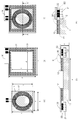
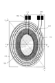
- FIG. 6 is a diagram showing dimensions of the coil unit of the embodiment. 6A shows only the first coil 12, FIG. 6B shows only the second coil 22, and FIG. 6C shows a coil unit in which the first coil 12 and the second coil 22 are stacked and combined (see FIG. 6). 1) and FIG. 6D each show a cross section of the coil unit shown in FIG.
- the long side a 48 mm
- the short side b 32 mm of the first magnetic body 11
- the outer diameter c 41 mm in the longitudinal direction of the first coil 12
- the outer diameter d 30 mm in the short direction
- the second magnetic body The long side e of the 21 and the second coil 22 is 41 mm
- the short side f 31 mm
- the thickness g of the coil unit in which these are laminated 1.5 mm.
- the outer peripheral dimensions of the two coils are substantially the same and overlap, and there is a region where the two coils do not overlap on the inner peripheral side.
- the first coil 12 is elliptical and the second coil 22 is rectangular, the four corners of the second coil 22 are regions that do not overlap.
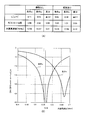
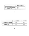
- FIG. 7 is a diagram showing the results of measuring the power transmission efficiency during contactless power transmission and the maximum communication distance during contactless wireless communication as the performance of the coil unit of the embodiment shown in FIG.
- FIG. 7A shows the measurement result of the power transmission efficiency
- FIG. 7B shows the measurement result of the maximum communication distance.
- the power transmission efficiency is not the transmission efficiency of only the coil, but the efficiency of the entire charging system including the AC power supply circuit of the charger as shown in FIG. 5 to the DC output of the portable wireless terminal.
- the power transmission efficiency was 40.3 [%]. In the state where the first coil 12 and the second coil 22 shown in FIG. 6C coexist, the power transmission efficiency was 40.4 [%]. In this case, two coils are stacked and coexisted, and even if the second coil 22 is disposed on the external device side of the first coil 12, performance degradation due to electromagnetic coupling does not occur in non-contact power transmission. .
- the maximum communication distance was 126 [mm], and the insensitive area (Null area) did not occur. Further, in the state where the first coil 12 and the second coil 22 shown in FIG. 6C coexist, the maximum communication distance is 127 [mm], and no dead area (Null area) is generated. In this case, two coils are stacked and coexisted, and even if the first coil 12 is disposed in the vicinity of the second coil 22, performance degradation due to electromagnetic coupling does not occur in non-contact wireless communication.
- the present embodiment when a plurality of coils of the first coil 12 and the second coil 22 coexist, electromagnetic coupling between the coils can be reduced, and performance degradation due to electromagnetic coupling can be suppressed. Further, by arranging a plurality of coils in a stacked manner, the arrangement area can be reduced, and a coil with little performance deterioration can be realized in a space-saving manner. For this reason, in the portable wireless terminal equipped with the coil unit including the coil for contactless wireless communication according to the present embodiment, it is possible to suppress performance degradation during both contactless power transmission and contactless wireless communication while achieving downsizing. The desired performance can be obtained with a space-saving coil unit.
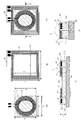
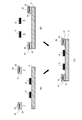
- FIG. 8A and 8B are diagrams showing the configuration of the coil unit according to the second embodiment of the present invention.
- FIG. 8A is a plan view of the coil unit
- FIG. 8B is an AA view of FIG.
- FIG. 8C is a cross-sectional view taken along the line BB ′ of FIG. 8A.
- symbol is attached
- the second embodiment is an example in which the shape of the first coil in the first embodiment is changed.
- 11 A of 1st magnetic bodies are formed in the square plate shape similarly to 1st Embodiment.
- the first coil 12 ⁇ / b> A is configured by a coil in which a conductor winding is wound in an annular shape with a square round shape.
- the second magnetic body 21A and the second coil 22A have substantially the same configuration as that of the first embodiment. That is, the second magnetic body 21A is formed in a square annular plate shape, and the second coil 22A is wound in a square annular shape by a conductor wiring pattern formed on a substrate 30A such as a glass epoxy substrate. Consists of coils.
- the first magnetic body 11A and the first magnetic body 11A are arranged in the arrow H direction from the lower side in the coil thickness direction (vertical direction in FIGS. 8B and 8C).
- the coil 12A, the second magnetic body 21A, the substrate 30A, and the second coil 22A are stacked in this order.
- the second coil 22A, the substrate 30A, the second magnetic body 21A, the first coil 12A, and the first magnetic body 11A are stacked in this order.
- the first coil 12A and the second coil 22A are arranged in a state where at least a part of the first coil 12A and the second coil 22A are overlapped so as to have a region that does not overlap the part. At this time, it arrange
- the electromagnetic coupling between the two coils can be reduced, and performance degradation due to the electromagnetic coupling can be suppressed.
- the two coils can be stacked and arranged to reduce the size.
- FIG. 9A and 9B are diagrams showing the configuration of a coil unit according to the third embodiment of the present invention.
- FIG. 9A is a plan view of the coil unit
- FIG. 9B is an AA view of FIG. 9A.
- FIG. 9C is a sectional view taken along the line BB ′ of FIG. 9A.
- symbol is attached
- the third embodiment is an example in which the shape of the second coil in the first embodiment is changed.
- the first magnetic body 11B and the first coil 12B have substantially the same configuration as in the first embodiment. That is, the first magnetic body 11B is formed in a rectangular plate shape, and the first coil 12B is configured by a coil formed by winding a conductor winding in an elliptical ring shape.
- the second magnetic body 21B is formed in an elliptical annular plate shape, and the second coil 22B is a coil that is wound in an elliptical shape by a conductor wiring pattern formed on a substrate 30B such as a glass epoxy substrate. Composed.
- the first magnetic body 11B and the first magnetic body 11B are arranged in the arrow H direction from the lower side in the coil thickness direction (vertical direction in FIGS. 9B and 9C).
- the coil 12B, the second magnetic body 21B, the substrate 30B, and the second coil 22B are stacked in this order.
- the second coil 22B, the substrate 30B, the second magnetic body 21B, the first coil 12B, and the first magnetic body 11B are stacked in this order.
- the first coil 12B and the second coil 22B are arranged in a state where at least a part of the first coil 12B and the second coil 22B are overlapped so as to have a region that does not overlap the part. At this time, it arrange
- the electromagnetic coupling between the two coils can be reduced, and performance degradation due to the electromagnetic coupling can be suppressed.
- the two coils can be stacked and arranged to reduce the size.
- FIG. 10 shows an example in which the inner diameter and the outer shape of the first coil and the second coil are the same.
- an elliptical annular first coil 12C and a square annular second coil 22C are stacked.
- a rectangular first round coil 12D and a rectangular second coil 22D are stacked and arranged.
- the first coil and the second coil are almost completely overlapped.
- FIG. 2 by providing a second magnetic body corresponding to the second coil between the first coil and the second coil. , Performance degradation due to electromagnetic coupling can be reduced.
- FIG. 11 shows an example in which the arrangement of both coils is changed when the first coil is an elliptical ring and the second coil is a square ring as in FIG.
- an elliptical annular first coil 12E and a rectangular annular second coil 22E are arranged so as to overlap each other on the outer peripheral sides of both sides in the coil longitudinal direction.
- an elliptical annular first coil 12F and a rectangular annular second coil 22F are arranged so as to overlap each other on the outer peripheral side of both sides in the coil lateral direction.
- an elliptical annular first coil 12G and a rectangular annular second coil 22G are arranged on the outer peripheral side of two adjacent sides.
- an elliptical annular first coil 12H and a rectangular annular second coil 22H are arranged on the outer peripheral side of one side.
- an elliptical annular first coil 12I and a rectangular annular second coil 22I are arranged on the outer peripheral side of three sides.
- a part of the outer periphery of the first coil overlaps with the second coil, but the second magnetic body corresponding to the second coil as shown in FIG.
- FIG. 12 shows an example in which the arrangement of the two coils is changed when the first coil is formed in a square round shape and the second coil is formed in a square shape as in FIG.
- a square-rounded annular first coil 12J and a rectangular-annular second coil 22J are arranged so as to overlap each other on the outer peripheral sides of both ends in the coil longitudinal direction.
- a square-rounded annular first coil 12K and a square-annular second coil 22K are arranged so as to overlap each other on the outer peripheral sides of both ends in the coil lateral direction.
- annular first coil 12L having a rounded rectangular shape and a square annular second coil 22L are arranged so as to overlap each other on the outer peripheral side of two adjacent sides.
- annular first coil 12M having a rounded rectangular shape and a square annular second coil 22M are arranged so as to overlap each other on the outer peripheral side of one side.
- a rectangular square-round annular first coil 12N and a rectangular annular second coil 22N are arranged on the outer peripheral side of three sides.
- a part of the outer periphery of the first coil overlaps the second coil, but corresponds to the second coil as shown in FIGS.
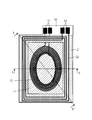
- FIG. 13A and 13B are diagrams showing the configuration of a coil unit according to a comparative example.
- FIG. 13A is a plan view of the coil unit
- FIG. 13B is a cross-sectional view taken along line AA ′ of FIG.
- the coil unit of the comparative example includes a first magnetic body 511, a first coil 512 that functions as a non-contact power transmission coil, and a second coil 522 that functions as a non-contact wireless communication coil.
- the first magnetic body 511 is formed in a rectangular plate shape, and the first coil 512 and the second coil 522 are disposed on one surface of the plate surface.
- the first coil 512 is constituted by a coil in which a conductor winding is wound in an elliptical ring shape, and receives power supplied from an external charger as a charging coil.
- the second coil 522 is formed of a coil that is wound in an elliptical ring shape by a conductor wiring pattern formed on a substrate 530 formed of a glass epoxy substrate or the like.
- the second coil 522 is a coil for non-contact wireless communication and transmits / receives data to / from an external device such as a reader / writer device.
- the second coil 522 is disposed on the outer peripheral side of the first coil 512, and the first coil 512 and the second coil 522 are positioned on substantially the same plane without overlapping.
- a first terminal 531 for the first coil 512 and a second terminal 532 for the second coil 522 are formed by a conductor wiring pattern.
- the first terminal 531 is connected to the first coil 512 through wiring
- the second terminal 532 is connected to the second coil 522 through a wiring pattern of the substrate 530.
- the first coil 512 and the second coil 522 are arranged without being stacked, and the second magnetic body is not provided. Therefore, the first coil 512 and the second coil 522 When close to each other, the electromagnetic coupling between both coils increases, and the performance is deteriorated due to the influence. For example, it has been confirmed that the maximum communication distance of non-contact wireless communication is deteriorated to 117 [mm]. It is difficult to improve the maximum communication distance of non-contact wireless communication using the coil unit.
- the second coil 522 outside the first coil 512 and arranging the two coils so as not to overlap the arrangement area of the coil increases, and the radio communication terminal mounting the coil unit becomes large. Become.
- the two coils are arranged so as to form a double ring, so that the arrangement area of the coils increases.
- performance degradation is expected due to electromagnetic coupling between the coils.
- performance such as power transmission efficiency and communication distance deteriorates due to electromagnetic coupling between the coils.
- the fourth to sixth embodiments have been made in view of the above-described conventional circumstances, and a plurality of coils such as a non-contact wireless communication coil and a non-contact power transmission coil coexist in the housing.
- a transmission coil and a portable wireless terminal that can easily achieve a reduction in the thickness of the casing while suppressing performance deterioration of each coil will be described.
- a transmission coil having a non-contact wireless communication coil and a non-contact power transmission coil is used as an example of a transmission coil according to the present invention and a portable wireless terminal equipped with the transmission coil.
- a transmission coil having a non-contact wireless communication coil and a non-contact power transmission coil is used as an example of a transmission coil according to the present invention and a portable wireless terminal equipped with the transmission coil.
- wireless terminal which mounts this coil unit and this coil unit is shown.
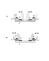
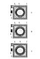
- FIG. 14 is a plan view showing a configuration of a coil unit according to the fourth embodiment.
- FIG. 15 is a cross-sectional view of the coil unit of the fourth embodiment.
- FIG. 15A is a cross-sectional view taken along the line AA ′ of FIG.
- FIG. 15B is a cross-sectional view taken along the line BB ′ in FIG.
- FIG. 15C is an enlarged view of an example of a region C in FIG.
- FIG. 15D is an enlarged view of another example of the region C in FIG.
- the direction of arrow H in FIG. 15A represents the direction of the inner wall side of the back casing of the portable wireless terminal in which the coil unit of this embodiment is mounted, and the direction opposite to arrow H in FIG.
- the direction inside the housing of the wireless terminal that is, the direction on the front casing side is represented.
- coil thickness direction the direction of arrow H or the direction opposite to arrow H
- coil surface direction the direction orthogonal to the coil thickness direction
- the coil unit of this embodiment includes a first magnetic body 11 having a predetermined magnetic permeability, a first coil 12 functioning as a non-contact power transmission coil, and a magnetic permeability different from the predetermined magnetic permeability of the first magnetic body 11. And a second coil 22 functioning as a non-contact wireless communication coil.
- the first magnetic body 11 is provided corresponding to the first coil 12
- the second magnetic body 21 is provided corresponding to the second coil 22.
- the first magnetic body 11 is formed in a rectangular plate shape, the first coil 12 is disposed on one surface of the plate surface (the inner wall side of the back casing of the portable wireless terminal), and the other plate surface (the portable wireless terminal).
- a battery pack, a shield case (not shown), or the like is disposed on the surface of the inside of the housing.
- the first magnetic body 11 is configured using a material having a magnetic permeability higher than 1, such as ferrite.
- the first coil 12 is configured using a coil in which a conductor winding is wound in an elliptical ring shape, and receives power supplied (transmitted) from an external charger as a charging coil.
- the resonance frequency f1 of the first coil 12 is a frequency adjusted using a capacitor or the like connected in parallel or in series with the first coil 12, and is, for example, about f1 ⁇ 100 kHz.
- the outer diameter of the first magnetic body 11 and the outer diameter of the first coil 12 are substantially the same.
- the second magnetic body 21 is formed in a square annular plate shape, and is opposite to the arrow H in FIG. 15A of the substrate 30 on one surface of the plate (the inner wall side of the back casing of the portable wireless terminal).
- a second coil 22 mounted on the direction side (inside the casing of the portable wireless terminal) is disposed.
- the second magnetic body 21 has a spacer (not shown) formed in a plate shape of a square environment on the other side of the plate surface (inside the casing of the portable wireless terminal).
- One of the plate surfaces of the spacer (the inner wall side of the rear case of the portable wireless terminal) and the other plate surface of the second magnetic body 21 (the inner side of the case of the portable wireless terminal) are in contact.
- the spacer is disposed so that the other surface (inside the casing of the portable wireless terminal) of the first magnetic body 11 and the other surface of the spacer (inside the casing of the portable wireless terminal) are flush. Is done.
- the second magnetic body 21 is arranged such that the entire plate surface is located outside the outer peripheral portion of the first magnetic body 11 in the coil surface direction.
- the second magnetic body 21 is configured using a material having a magnetic permeability higher than 1, such as ferrite.
- ⁇ r2 10 to 300 is used.
- the second boundary surface B2 between the second magnetic body 21 and the second coil 22 is a coil thickness direction from the first boundary surface B1 between the first magnetic body 11 and the first coil 12. In particular in the direction of the arrow H (see FIG. 15C).
- the first boundary surface B1 between the first magnetic body 11 and the first coil 12 and the second boundary surface B2 between the second magnetic body 21 and the second coil 22 may be substantially the same plane ( (See FIG. 15D).
- the second coil 22 is wound in a square ring shape by a conductor wiring pattern formed on the surface of the substrate 30 on the side opposite to the arrow H in FIG. 15A (inside the casing of the portable wireless terminal). It is comprised using the coil which consists of.
- the second coil 22 is a non-contact wireless communication coil and transmits / receives data to / from an external device such as a reader / writer device.
- the resonance frequency f2 of the second coil 22 is a frequency adjusted using a capacitor or the like connected in parallel or in series with the second coil 22, and is, for example, about f2 ⁇ 13.56 MHz.
- the outer diameter of the second magnetic body 21 and the outer diameter of the second coil 22 are substantially the same.
- the substrate 30 is formed by using, for example, a glass epoxy resin or a flexible printed circuit board, and is formed of, for example, an ABS (AcrylonitrilerylButadiene Styrene) resin on the surface in the direction of arrow H in FIG.
- a rear housing is arranged.
- a pair of first terminals 31 for the first coil 12 and a pair of second terminals 32 for the second coil 22 are formed at one end of the substrate 30 by a conductor wiring pattern.
- the first terminal 31 is connected to the first coil 12 through a wiring pattern
- the second terminal 32 is connected to the second coil 22 through the wiring pattern of the substrate 30.
- FIGS. 15A to 15D show wiring patterns from the first terminal 31 and the second terminal 32 to the first coil 12 and the second coil 22 in order to avoid complication of the drawings. Is omitted.
- the coil unit of the present embodiment has a second boundary surface in the coil thickness direction (vertical direction in FIG. 2) from the lower side of FIG. 15 to the arrow H direction (the direction of the inner wall side of the back casing of the portable wireless terminal).
- the first magnetic body 11 and the second magnetic body 21 are arranged such that B2 is above the first boundary surface B1 (in the direction indicated by the arrow H in FIG. 15) or substantially in the same plane, and on the surface of the first magnetic body 11
- the 1st coil 12 is laminated
- the second coil 22 and the substrate are arranged in the arrow H direction (the direction of the inner wall side of the back casing of the portable wireless terminal) from the lower side of FIG. Laminated in the order of 30.
- the rear casing of the portable wireless terminal is positioned further in the direction of arrow H from the substrate 30, and the coil unit is housed and provided in the casing. Therefore, when viewed from the external device side, that is, from the inner wall side of the back casing of the portable wireless terminal, the substrate 30, the second coil 22, and the second magnetic body 21 are stacked in this order, and the second boundary surface B2 is the first boundary surface B2.
- the second magnetic body 21 and the first magnetic body 11 are arranged so as to be above the boundary surface B1 (in the direction of arrow H in FIG. 15) or substantially on the same plane, and the first coil 12 and the first magnetic body 11 are stacked in this order. Arranged.
- the first coil 12 and the second coil 22 are preferably arranged so as not to overlap in the thickness direction of the coil.
- the first coil 12 has an oval shape and the second coil 22 has a rectangular shape, the four coil portions of the second coil 22 are non-overlapping regions. Located on the outside. With such a configuration, electromagnetic coupling between both coils can be reduced.
- the first coil 12 is a coil in which the conductor winding is wound in an elliptical ring shape, but the conductor winding is wound in a square ring shape having bending radii at four corners. May be.
- the relationship between the resonance frequencies of the first coil 12 and the second coil 22 is such that the resonance frequency of the first coil 12 is lower than the resonance frequency of the second coil 22 (f1 ⁇ f2).
- the relationship between the magnetic permeability of the first magnetic body 11 and the second magnetic body 21 is such that the permeability of the first magnetic body 11 is higher than the permeability of the second magnetic body 21 (relative magnetic permeability ⁇ r1> ⁇ r2). Is preferable.
- FIG. 16A is a diagram showing the magnetic field distribution of the coil unit at the time of operation of the first coil 12 at the position of the cross section along the line AA ′ of FIG. 14 (position of FIG. 15A).
- FIG. 16B is a diagram showing the magnetic field distribution of the coil unit at the time of the operation of the second coil 22 at the position of the cross section along line AA ′ of FIG. 14 (position of FIG. 15A).
- FIG. 17A is a diagram showing the magnetic field distribution of the coil unit at the time of the operation of the first coil 12 at the position of the cross section along line BB ′ of FIG. 14 (position of FIG. 15B).
- FIG. 15A is a diagram showing the magnetic field distribution of the coil unit at the time of the operation of the first coil 12 at the position of the cross section along line BB ′ of FIG. 14 (position of FIG. 15B).
- 17B is a diagram showing the magnetic field distribution of the coil unit at the time of the operation of the second coil 22 at the position of the cross section along line BB ′ of FIG. 14 (position of FIG. 15B). 16 and 17, the illustration of the spacer is omitted for the sake of simplicity.
- the magnetic lines of force pass through the first magnetic body 11 in the vicinity of the first coil 12.
- a magnetic field is generated so as to enter the space. In this case, the influence of the magnetic field from the first coil 12 to the second coil 22 is small.
- the magnetic lines of force are generated near the second coil 22 in the second magnetic body.
- a magnetic field is generated so as to pass through 21 and exit into space. In this case, the influence of the magnetic field from the second coil 22 to the first coil 12 is small.
- the coil unit of the present embodiment has a region where the first coil 12 and the second coil 22 do not overlap, electromagnetic coupling between the coils is reduced.
- electromagnetic coupling can be made sufficiently small in the four corner regions of the coil where the two coils do not overlap as shown in FIGS.
- FIG. 18 is a block diagram showing a configuration of a portable wireless terminal equipped with the coil unit of the present embodiment, a charger as an external device, and a reader / writer device.
- the portable wireless terminal 50 includes a first coil 12 for charging and a second coil 22 for non-contact wireless communication.
- the first coil 12 is connected to the contactless charging unit 51, and the second coil 22 is connected to the contactless wireless communication unit 52.
- the first coil 12 is connected in parallel with the capacitor 54, and further connected to the rectifier circuit 55 of the non-contact charging unit 51.
- the second coil 22 is connected in parallel with the capacitor 56 and further connected to the modulation / demodulation circuit 57 of the non-contact wireless communication unit 52.
- the non-contact charging unit 51 and the non-contact wireless communication unit 52 are connected to a control circuit 53, and the operation of each unit is controlled by the control circuit 53.
- the charger 60 includes a non-contact power transmission coil 63.
- the non-contact power transmission coil 63 is connected in parallel with the capacitor 64 and further connected to the AC power supply circuit 61.
- the AC power supply circuit 61 is connected to the control circuit 62, and the output of AC power for charging is controlled by the control circuit 62.
- the reader / writer device 70 includes a non-contact wireless communication coil 73.
- the non-contact wireless communication coil 73 is connected in parallel with the capacitor 74 and further connected to the modulation / demodulation circuit 71.
- the modulation / demodulation circuit 71 is connected to the control circuit 72, and the control circuit 72 controls the data modulation and demodulation operations by non-contact wireless communication.
- the non-contact power transmission coil 63 of the charger 60 and the first coil 12 of the portable wireless terminal 50 are disposed close to each other and faced to each other. Power is supplied from 60 to the portable wireless terminal 50. At this time, the non-contact power transmission coil 63 and the first coil 12 are electromagnetically coupled, and charging power is transmitted in a non-contact manner through both coils.
- the AC power generated and output in the AC power supply circuit 61 is transmitted from the non-contact power transmission coil 63 to the first coil 12 and is received by the portable radio terminal 50.
- the transmitted AC power is rectified by the rectifier circuit 55 and converted into DC power, and the DC output is supplied to the battery unit 58 for charging. Note that it is also possible to supply a direct current output to a circuit in the portable wireless terminal 50 to serve as an operating power source for each unit.
- the non-contact wireless communication coil 73 of the reader / writer device 70 and the second coil 22 of the portable wireless terminal 50 are arranged close to each other so as to face each other. Data is transmitted to and received from the wireless terminal 50.
- the non-contact wireless communication coil 73 and the second coil 22 are electromagnetically coupled, and data transmission of non-contact wireless communication is performed via both coils.
- Data transmitted from the reader / writer device 70 to the portable wireless terminal 50 is modulated by the modulation / demodulation circuit 71, transmitted from the non-contact wireless communication coil 73 to the second coil 22, and received by the portable wireless terminal 50.
- the transmitted data is demodulated in the modulation / demodulation circuit 57 of the portable radio terminal 50.
- Data transmitted from the portable wireless terminal 50 to the reader / writer device 70 is modulated by the modulation / demodulation circuit 57, transmitted from the second coil 22 to the non-contact wireless communication coil 73, and received by the reader / writer device 70.
- the transmitted data is demodulated by the modulation / demodulation circuit 71 of the reader / writer device 70. In this way, using the contactless wireless communication function of the portable wireless terminal 50, data can be written to and read from the reader / writer device 70 to the portable wireless terminal 50 by contactless wireless communication.
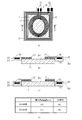
- FIG. 19A and 19B are diagrams illustrating an example of dimensions of the coil unit according to the embodiment.
- FIG. 19C is a plan view of the coil unit according to the embodiment.
- FIG. 19D is a cross-sectional view taken along line AA ′ in FIG.
- FIG. 19E is an enlarged view of a region D in FIG. 19A shows only the first coil 12 laminated on the surface of the first magnetic body 11, and
- FIG. 19B shows only the second coil 22 laminated on the surface of the second magnetic body 21
- 19 (C) is a coil unit in which the first coil 12 and the second coil 22 are combined and coexisted
- FIG. 19 (D) is the coil unit shown in FIG. 19 (C).
- FIG. 19E is an enlarged view of the first boundary surface B1 and the second boundary surface B2 in FIG. 19D, with a cross section (illustration of the spacer provided so as to contact the second magnetic body 21 is omitted). Respectively.
- the coil unit according to the example is formed so that the first boundary surface B1 and the second boundary surface B2 are substantially on the same plane.
- the outer peripheral dimensions of the first magnetic body 11 and the first coil 12 and the outer peripheral dimensions of the second magnetic body 21 and the second coil 22 are substantially coincident with each other, and the first coil 12 and the second coil overlap. 22 is provided so as not to overlap.
- the distance between the first coil 12 and the second coil 22 is large at the four corners of the second coil 22.
- FIG. 20A is a diagram illustrating a result of measuring the power transmission efficiency during non-contact power transmission as the performance of the coil unit according to the example.
- FIG. 20B is a diagram illustrating a result of measuring a maximum communication distance during non-contact wireless communication as the performance of the coil unit according to the example.
- the efficiency of the entire charging system including the direct current input of the AC power supply circuit of the charger as shown in FIG. 18 to the direct current output of the portable wireless terminal as shown in FIG.
- the power transmission efficiency was 38.2 [%]. In the state where the first coil 12 and the second coil 22 shown in FIG. 19D coexist, the power transmission efficiency was 38.1 [%]. In this case, it can be seen that the two coils coexist, and even if the second coil 22 is disposed outside the first coil 12, performance degradation due to electromagnetic coupling does not occur in non-contact power transmission.
- the maximum communication distance was 141 [mm], and no dead area (Null area) occurred. Further, in the state where the first coil 12 and the second coil 22 shown in FIG. 19D coexist, the maximum communication distance is 128 [mm], and no dead area (Null area) is generated. In this case, two coils coexist, and if the first coil 12 is disposed in the vicinity of the second coil 22, performance degradation due to electromagnetic coupling occurs in non-contact wireless communication, but compared to a comparative example described later. It can be seen that the absolute value of the maximum communication distance is large.
- FIGS. 21A and 21B are diagrams illustrating an example of dimensions of a coil unit according to a comparative example.
- FIG. 21C is a plan view of a coil unit according to a comparative example.
- FIG. 21D is a cross-sectional view taken along line AA ′ in FIG.
- FIG. 21E is an enlarged view of a region E in FIG. 21A shows only the first coil 12 laminated on the surface of the first magnetic body 11, and FIG.
- FIG. 21B shows only the second coil 22 laminated on the surface of the second magnetic body 21
- 21 (C) is a coil unit in which the first coil 12 and the second coil 22 are combined and coexisted
- FIG. 21 (D) is the coil unit shown in FIG. 21 (C).
- the cross section, FIG. 21E shows enlarged views of the first boundary surface B1 and the second boundary surface B2 of FIG. 21D, respectively.
- the first coil 12 and the second coil 22 are provided so as not to overlap.
- the distance between the first coil 12 and the second coil 22 is large at the four corners of the second coil 22.
- FIG. 22 (A) is a diagram showing the results of measuring the power transmission efficiency during non-contact power transmission as the performance of the coil unit according to the comparative example.
- FIG. 22B is a diagram illustrating a result of measuring the maximum communication distance during non-contact wireless communication as the performance of the coil unit according to the comparative example.
- the power transmission efficiency the efficiency of the entire charging system including the direct current input of the AC power supply circuit of the charger as shown in FIG. 18 to the direct current output of the portable wireless terminal as shown in FIG.
- the power transmission efficiency was 38.1 [%]. In the state where the first coil 12 and the second coil 22 shown in FIG. 21D coexist, the power transmission efficiency was 38.0 [%]. In this case, it turns out that there is no big difference regarding the power transmission performance in the coil unit which concerns on an Example, and the coil unit which concerns on a comparative example.
- the second magnetic body In the state of the second coil 22 alone in which the first coil 12 is removed from FIG. 21D, the second magnetic body is not provided and the second coil 22 is in close contact with the first magnetic body. Although it remained at 130 [mm], the dead area (Null area) did not occur. In the state where the first coil 12 and the second coil 22 shown in FIG. 21D coexist, the maximum communication distance is 117 [mm], and no dead area (Null area) is generated. In this case, two coils coexist, and the maximum communication distance is deteriorated due to electromagnetic coupling between the coils.
- the coil unit provides the second magnetic body 21 corresponding to the second coil 22 outside the first magnetic body 11 corresponding to the first coil 12, and the first coil 12 and the first magnetic body.
- 11 and the second boundary surface B2 between the second coil 22 and the second magnetic body 21 are substantially the same plane, or the second boundary surface B2 is thicker than the first boundary surface B1.
- the present embodiment when a plurality of coils of the first coil 12 and the second coil 22 coexist in the housing, electromagnetic coupling between the coils can be reduced, and performance degradation due to electromagnetic coupling can be suppressed. .
- the coils close to each other in such a configuration in which a plurality of magnetic bodies are arranged in parallel to the coil, it is possible to provide a coil with little performance deterioration, and to easily realize a reduction in the thickness of the casing. Can do.
- both the contactless power transmission and the contactless wireless communication are performed while downsizing the portable wireless terminal. It is possible to obtain desired performance (power transmission performance, communication performance) by using a coil unit that can suppress performance degradation and can easily reduce the thickness of the casing of the portable wireless terminal.
- FIG. 23 is a plan view showing a configuration of a coil unit according to the fifth embodiment.
- FIG. 24A is a cross-sectional view taken along the line AA ′ of FIG.
- FIG. 24B is a cross-sectional view taken along the line BB ′ in FIG.
- 24A and 24B illustrate the wiring patterns from the first terminal 31 and the second terminal 32 to the first coil 12 and the second coil 22 in order to avoid complication of the drawings. Is omitted.
- the fifth embodiment is an example in which the shapes of the second magnetic body 21 and the second coil 22 in the fourth embodiment are changed.
- 11 A of 1st magnetic bodies and 12 A of 1st coils are the structures substantially the same as 4th Embodiment. That is, the first magnetic body 11A is formed in a rectangular plate shape, and the first coil 12A is configured by using a coil in which a conductor winding is wound in an elliptical ring shape.
- the second magnetic body 21A is formed in an elliptical annular plate shape, and the second coil 22A is wound in an elliptical shape by a conductor wiring pattern formed on the surface of the substrate 30A in the direction opposite to the arrow H in FIG. It is comprised using the coil formed.
- the coil unit of the present embodiment has an arrow H direction (portable radio) from the lower side of FIG. 24 in the coil thickness direction (vertical direction in FIGS. 24A and 24B).
- the first magnetic body 11A and the second magnetic body are arranged such that the second boundary surface B2 is above the first boundary surface B1 (in the direction of the arrow in FIG. 15) or substantially in the same plane (in the direction of the inner wall side of the rear casing of the terminal).
- 21A, and the first coil 12A is stacked on the surface of the first magnetic body 11A.
- the second coil 22A the substrate, from the lower side in FIG. Laminated in the order of 30A.
- the substrate 30A, the second coil 22A, and the second magnetic body 21A are stacked in this order, and the second boundary surface B2 is the first boundary surface.
- the first magnetic body 11A and the second magnetic body 21A are arranged so as to be above B1 (in the direction of the arrow in FIG. 24) or substantially on the same plane, and further, the first coil 12A and the first magnetic body 11A are stacked in this order. Be placed.
- the first coil 12A and the second coil 22A are arranged so as not to overlap in the thickness direction of the coil.
- FIG. 25 is a diagram illustrating a change in communication performance of the second coil 22 when the position of the second magnetic body 21 varies in the thickness direction of the coil.
- FIG. 25A is a plan view showing the configuration of the coil unit of the fourth embodiment.
- FIG. 25B is a cross-sectional view taken along line AA ′ in FIG.
- FIG. 25C is a cross-sectional view taken along line AA ′ in FIG.
- FIG. 25D shows the second coil 22 in a state where the position of the second magnetic body 21 varies in the direction in which the communication performance increases in the coil thickness direction and in a state in which the communication performance decreases. It is a figure which shows the comparison result of each communication performance.
- the reference numerals of the respective parts of the coil unit will be described using the same reference numerals as those of the coil unit of the fourth embodiment.
- FIG. 25B shows a case where the first boundary surface B1 and the second boundary surface B2 are substantially the same plane in the coil surface direction.
- the second boundary surface B2 is located below the first boundary surface B1 in the coil surface direction, and the bottom surface (lower surface) of the first magnetic body 11 and the bottom surface of the second magnetic body 21.
- (lower surface) is substantially in the same plane in the surface direction of the coil is shown.
- the bottom surfaces (lower surfaces) of the first magnetic body 11 and the second magnetic body 21 are in contact with flat surfaces of other members (not shown).
- FIG. 26 is a diagram showing a configuration of a coil unit according to the sixth embodiment.
- FIG. 26A is a plan view showing the configuration of the coil unit. Since the first magnetic body 11, the first coil 12, the second coil 22, and the substrate 30 constituting the present embodiment are the same as those of the coil unit of the first embodiment, the description thereof will be omitted by using the same reference numerals.
- the second magnetic bodies 21B and 21C are formed in a square plate shape, similarly to the second magnetic body 21 of the first embodiment.
- FIGS. 26B and 26C are cross-sectional views taken along the line AA ′ of FIG.
- the arrangement of the second magnetic body 21B is devised so that the position of the second magnetic body 21B does not vary in the direction in which the communication performance decreases in the thickness direction of the coil.
- a spacer 25 as a position regulating member for regulating the position of the second magnetic body 21B is disposed so as to contact the bottom surface (lower surface) of the second magnetic body 21B.
- the bottom surface (lower surface) of the first magnetic body 11 and the bottom surface (lower surface) of the spacer 25 abut against the surface of the other member 40.
- the position of the second magnetic body 21B does not vary in the direction in which the communication performance decreases in the thickness direction of the coil, but is fixed on the surface of the other member 40, and the second boundary surface B2 is fixed to the first boundary surface B1. It is not lower in the coil surface direction.
- the other member 40 is, for example, a battery pack, a shield case, an inner wall of the housing, or the like.
- the spacer 25 is formed in the shape of a square annular plate like the second magnetic body 21B.
- the shape of the spacer 25 is not limited to a square annular plate configuration as long as the position of the second magnetic body 21B can be regulated. For example, only the four corners of the bottom surface (lower surface) of the second magnetic body 21B are used. It may be in the form of a block as arranged in
- the spacer 25 may be formed of metal, resin, substrate (glass epoxy substrate, flexible substrate) or the like, and the material is not particularly limited.
- the thickness of the second magnetic body 21C in the thickness direction of the coil is set to be equal to or greater than the thickness of the first magnetic body 11B instead of arranging the spacer 25.
- the position of the second magnetic body 21B does not vary in the direction in which the communication performance decreases in the thickness direction of the coil, but is fixed on the surface of the other member 40, and the second boundary surface B2 is fixed to the first boundary surface B1. It is not lower in the coil surface direction.
- FIG. 27 is a diagram illustrating a configuration of the coil unit in the case where the spacer 25 is disposed so as to be in contact with the bottom surface (lower surface) of the second magnetic body 21B as the first embodiment.
- 27A and 27B are diagrams illustrating an example of dimensions of the coil unit according to the first embodiment.
- FIG. 27C is a plan view of the coil unit according to the first embodiment.
- FIG. 27D is a cross-sectional view taken along line AA ′ in FIG.
- FIG. 27E is an enlarged view of a region g in FIG.
- FIG. 27A shows the first coil 12 laminated on the surface of the first magnetic body 11
- FIG. 27B shows the second coil 22 laminated on the surface of the second magnetic body 21B.
- the description of the substrate 30 is omitted because it is the same as FIG.
- FIG. 27C is a coil unit according to the first embodiment in which the first coil 12 and the second coil 22 are combined and coexisted
- FIG. 27D is an AA of the coil unit shown in FIG. A cross-sectional view taken along the line ′
- FIG. 27E shows an enlarged view of the first boundary surface B1 and the second boundary surface B2 of FIG.
- the coil unit according to the first embodiment is formed so that the first boundary surface B1 and the second boundary surface B2 are substantially in the same plane.
- the coil unit thickness e was set to 0.8 mm.
- the outer peripheral dimensions of the first magnetic body 11 and the first coil 12 and the outer peripheral dimensions of the second magnetic body 21B and the second coil 22 are substantially coincident with each other, and the first coil 12 and the second coil overlap. 22 is provided so as not to overlap.
- the first coil 12 is circular and the second coil 22 is square, the distance between the first coil 12 and the second coil 22 is large at the four corners of the second coil 22.
- the bottom surface (lower surface) of the second magnetic body 21B in order to prevent the position of the second magnetic body 21B from varying in the direction in which the communication performance is lowered in the thickness direction of the coil, the bottom surface (lower surface) of the second magnetic body 21B.
- a spacer 25 for restricting the position of the second magnetic body 21B is disposed so as to abut.
- the bottom surface (lower surface) of the first magnetic body 11 and the bottom surface (lower surface) of the spacer 25 become a uniform plane, and other members 40 (for example, a battery pack, a shield case, an inner wall of the housing, etc.) that face each other. The surface is in contact with the surface.
- FIG. 28 is a diagram illustrating a configuration of the coil unit according to the second embodiment when the thickness of the second magnetic body 21C is substantially equal to the thickness of the first magnetic body 11.
- 28A and 28B are diagrams illustrating an example of dimensions of the coil unit according to the second embodiment.
- FIG. 28C is a plan view of the coil unit according to the second embodiment.
- FIG. 28D is a cross-sectional view taken along line AA ′ in FIG.
- FIG. 28E is an enlarged view of a region h in FIG.
- the dimensions of the coil unit according to Example 2 are the same as the dimensions of the coil unit according to Example 1 described above except that the spacer 25 is omitted and the thickness of the second magnetic body is different. Therefore, the description of FIGS. 28A to 28C is omitted.
- FIG. 28D is a cross-sectional view of the coil unit according to the second embodiment shown in FIG. 28C
- FIG. 28E is a region h of FIG. 28D, that is, the first boundary surface B1 and the second boundary surface.
- the enlarged view with B2 is shown, respectively.
- the thickness of the second magnetic body 21C is substantially equal to the thickness of the first magnetic body 11. Therefore, the bottom surface (lower surface) of the second magnetic body 21C and the bottom surface (lower surface) of the first magnetic body 11 are a uniform plane, and other members 40 (for example, a battery pack, a shield case, an inner wall of the housing, etc.) that face each other. ) In contact with the flat surface.
- other members 40 for example, a battery pack, a shield case, an inner wall of the housing, etc.
- FIG. 29 is a diagram showing the results of measuring the power transmission efficiency during non-contact power transmission and the maximum communication distance during non-contact wireless communication as the performance of each coil unit according to the first and second embodiments.
- FIG. 29A shows the measurement result of power transmission efficiency.
- FIG. 29B shows the measurement result of the maximum communication distance.
- the power transmission efficiency the efficiency of the entire charging system including the direct current input of the AC power supply circuit of the charger as shown in FIG. 18 to the direct current output of the portable wireless terminal as shown in FIG.
- the power transmission efficiency that is, the charging efficiency by the first coil 12 is 38.1 [%]. there were.
- the charging efficiency by the first coil 12 is 38.2 [%] and 38.1 [%], respectively. there were. Thus, it can be seen that there is no difference in power transmission efficiency between the coil units.
- the maximum communication distance is 128 [mm], and a dead area (Null area) is generated. There wasn't.
- the maximum communication distance by the second coil 22 is 128 [mm], respectively, and a dead area (Null area) ) Did not occur.
- the second boundary surface B2 is positioned below the first boundary surface B1 in the thickness direction of the coil due to variations in the position of the second magnetic body. The maximum communication distance was 117 [mm].
- the spacer 25 is interposed so as to contact the bottom surface (lower surface) of the second magnetic body 21B, or the thickness of the second magnetic body 21C is made to be the first magnetic body.
- the thickness By setting the thickness to 11 or more, the positions of the second magnetic bodies 21B and 21C in the coil thickness direction are restricted.
- the coil unit of this embodiment can suppress that the position of the second magnetic body varies in the direction in which the communication performance decreases in the thickness direction of the coil, and the communication performance (for example, the maximum communication distance) of the second coil. ) Can be stabilized.
- FIG. 30 is a cross-sectional view showing the configuration of the coil unit when the surface of the other member 40 is not a flat surface.
- FIG. 30A and 30B show that the surface 40A1 on the second magnetic body 21B side of the surface of the other member 40A is higher in the thickness direction of the coil than the surface 40A2 on the first magnetic body 11B side. Sectional drawing in the case of being located is shown.
- the sum of the height of the step m of the other member 40A, the thickness of the spacer 25, and the thickness of the second magnetic body 21B is set to be equal to or greater than the thickness of the first magnetic body 11B.
- the sum of the height of the step m of the other member 40A and the thickness of the second magnetic body 21C is set to be equal to or greater than the thickness of the first magnetic body 11B.
- FIGS. 30C and 30D the surface 40A3 on the second magnetic body 21C side in the surface of the other member 40B is compared with the surface 40A4 on the first magnetic body 11C side in the thickness direction of the coil. Sectional drawing in the case of being located below is shown.
- the sum of the thickness of the spacer 25 and the thickness of the second magnetic body 21C is equal to or greater than the sum of the thickness of the first magnetic body 11C and the height of the step n of the other member 40B.
- the thickness of the second magnetic body 21C is configured to be equal to or greater than the sum of the thickness of the first magnetic body 11C and the height of the step n of the other member 40B.
- the second boundary surface B2 is the second boundary surface B2 in consideration of the level difference of the surface of the other member 40.
- the coil shape may be any shape such as a quadrangle, a circle, and an ellipse, and is not particularly limited.
- the spacer 25 is disposed when the thickness of the second magnetic body 21 is equal to or less than the thickness of the first magnetic body 11, but the thickness of the second magnetic body 21 is the first thickness. Even if the thickness is equal to or greater than the thickness of the first magnetic body 11, a spacer may be disposed below the second magnetic body 21. Similarly, the communication performance of the second coil 22 can be stabilized.
- the coil unit is described as being arranged in the vertical direction in order to make the description easy to understand.
- the coil unit may be arranged in an arbitrary direction such as a horizontal direction.
- the two coils are arranged so as to form a double ring, so that the arrangement area of the coils increases.
- performance degradation is expected due to electromagnetic coupling between the coils.
- performance such as power transmission efficiency and communication distance deteriorates due to electromagnetic coupling between the coils.
- Patent Document 1 does not mention simplification of the manufacturing process of the wireless card when two coils are used.
- Mobile wireless terminals including the above-described contactless charging function and contactless wireless communication function are likely to be widely used in the future.
- the performance deterioration of the two coils is suppressed and simplified. It is considered that the arrangement of each coil so that it can be manufactured is required.
- a transmission coil having a non-contact wireless communication coil and a non-contact power transmission coil is used as an example of a transmission coil according to the present invention and a portable wireless terminal equipped with the transmission coil.
- a transmission coil having a non-contact wireless communication coil and a non-contact power transmission coil is used as an example of a transmission coil according to the present invention and a portable wireless terminal equipped with the transmission coil.
- wireless terminal which mounts this coil unit and this coil unit is shown.
- FIG. 31 is a plan view showing a configuration of a coil unit according to the seventh embodiment.
- FIG. 32 is a cross-sectional view of the coil unit of the seventh embodiment.
- FIG. 32A is a cross-sectional view taken along the line AA ′ of FIG.
- FIG. 32B is a cross-sectional view taken along the line BB ′ of FIG.
- the direction of arrow H in FIG. 32A represents the direction of the inner wall side of the back casing of the portable wireless terminal on which the coil unit of this embodiment is mounted, and the direction opposite to arrow H in FIG. This represents the direction inside the housing of the wireless terminal, that is, the direction of the front casing.
- the coil unit of this embodiment includes a first magnetic body 11 having a predetermined magnetic permeability, a first coil 12 functioning as a non-contact power transmission coil, and a magnetic permeability different from the predetermined magnetic permeability of the first magnetic body 11. And a second coil 22 functioning as a non-contact wireless communication coil.
- the first magnetic body 11 is provided corresponding to the first coil 12
- the second magnetic body 21 is provided corresponding to the second coil 22.
- the first magnetic body 11 is formed in a rectangular plate shape, the first coil 12 is disposed on one surface of the plate surface (the inner wall side of the back casing of the portable wireless terminal), and the other plate surface (the portable wireless terminal).
- a battery pack, a shield case (not shown), or the like is disposed on the surface of the inside of the housing.
- the first magnetic body 11 is configured using a material having a magnetic permeability higher than 1, such as ferrite.
- the first coil 12 is configured using a coil in which a conductor winding is wound in an elliptical ring shape, and receives power supplied (transmitted) from an external charger as a charging coil.
- the resonance frequency f1 of the first coil 12 is a frequency adjusted using a capacitor or the like connected in parallel or in series with the first coil 12, and is, for example, about f1 ⁇ 100 kHz.
- the second magnetic body 21 is formed in a rectangular annular plate shape, and one of the plate surfaces (inside the casing of the portable wireless terminal) is one of the plate surfaces of the first magnetic body 11 (inner wall of the rear casing of the portable wireless terminal). It is arranged so as to abut on the surface of the side. Further, the second magnetic body 21 is placed on the other side of the plate surface (the inner wall side of the rear casing of the portable wireless terminal) on the opposite side of the arrow 30 in FIG. A second coil 22 mounted on the inside of the housing is disposed. Furthermore, the entire surface of the second magnetic body 21 is disposed outside the outer peripheral portion of the first coil 12, and the outer diameter of the second magnetic body 21 and the outer diameter of the first magnetic body 11 are substantially the same. is there.
- the second coil 22 is wound in a square ring shape by a conductor wiring pattern formed on the surface of the substrate 30 on the side opposite to the arrow H in FIG. 32 (A) (inside the casing of the portable wireless terminal). It is comprised using the coil which consists of.
- the second coil 22 is a non-contact wireless communication coil and transmits / receives data to / from an external device such as a reader / writer device.
- the resonance frequency f2 of the second coil 22 is a frequency adjusted using a capacitor or the like connected in parallel or in series with the second coil 22, and is, for example, about f2 ⁇ 13.56 MHz.
- the substrate 30 is formed using, for example, a glass epoxy resin, and a rear housing of a portable wireless terminal formed of, for example, ABS (Acrylonitrile Butadiene Styrene) resin on the surface in the direction of arrow H in FIG. Be placed.
- a pair of first terminals 31 for the first coil 12 and a pair of second terminals 32 for the second coil 22 are formed at one end of the substrate 30 by a conductor wiring pattern.
- the first terminal 31 is connected to the first coil 12 through a wiring pattern
- the second terminal 32 is connected to the second coil 22 through the wiring pattern of the substrate 30.
- FIGS. 32A and 32B the wiring patterns from the first terminal 31 and the second terminal 32 to the first coil 12 and the second coil 22 are shown in order to avoid complication of the drawing. Is omitted.
- the coil unit of the present embodiment includes a first magnetic body in the thickness direction of the coil (vertical direction in FIG. 32) from the lower side of FIG. 32 in the direction of arrow H (direction on the inner wall side of the back casing of the portable wireless terminal). 11.
- the first coil 12 and the second magnetic body 21 are laminated on the surface of the first magnetic body 11.
- the second coil 22 and the substrate are arranged in the arrow H direction (the direction of the inner wall side of the back casing of the portable wireless terminal) from the lower side of FIG. Laminated in the order of 30.
- the rear casing of the portable radio terminal is positioned in the direction of arrow H further than the second coil 22 and the coil unit is housed and provided in the casing. Therefore, when viewed from the external device side, that is, the inner wall side of the back casing of the portable wireless terminal, the substrate 30, the second coil 22, the second magnetic body 21, the first coil 12, and the first magnetic body 11 are laminated in this order. Be placed.
- the first coil 12 and the second coil 22 are preferably arranged so as not to overlap in the thickness direction of the coil.
- the four coil portions of the second coil 22 are non-overlapping regions. Located on the outside. With such a configuration, electromagnetic coupling between both coils can be reduced.
- the relationship between the resonance frequencies of the first coil 12 and the second coil 22 is such that the resonance frequency of the first coil 12 is lower than the resonance frequency of the second coil 22 (f1 ⁇ f2).
- the relationship between the magnetic permeability of the first magnetic body 11 and the second magnetic body 21 is such that the permeability of the first magnetic body 11 is higher than the permeability of the second magnetic body 21 (relative magnetic permeability ⁇ r1> ⁇ r2). Is preferable.
- FIG. 33A is a diagram showing the magnetic field distribution of the coil unit at the time of operation of the first coil 12 at the position of the cross section along line AA ′ of FIG. 31 (position of FIG. 32A).
- FIG. 33B is a diagram showing the magnetic field distribution of the coil unit at the time of operation of the second coil 22 at the position of the cross section along line AA ′ of FIG. 31 (position of FIG. 32A).
- 34A is a diagram showing the magnetic field distribution of the coil unit at the time of the operation of the first coil 12 at the position of the cross section along the line BB ′ of FIG. 31 (position of FIG. 32B).
- FIG. 34B is a diagram showing the magnetic field distribution of the coil unit at the time of operation of the second coil 22 at the position of the cross section along the line BB ′ of FIG. 31 (position of FIG. 32B).
- the lines of magnetic force pass through the first magnetic body 11 in the vicinity of the first coil 12.
- a magnetic field is generated so as to enter the space. In this case, the influence of the magnetic field from the first coil 12 to the second coil 22 is small.
- the magnetic lines of force are generated near the second coil 22 in the second magnetic body.
- a magnetic field is generated so as to pass through 21 and exit into space. In this case, the influence of the magnetic field from the second coil 22 to the first coil 12 is small.
- the coil unit of the present embodiment has a region where the first coil 12 and the second coil 22 do not overlap, electromagnetic coupling between the coils is reduced.
- the electromagnetic coupling can be made sufficiently small in the four corner regions of the coil where the coils do not overlap as shown in FIGS. 34 (A) and 34 (B).
- FIG. 35 is a block diagram showing a configuration of a portable wireless terminal equipped with the coil unit of the present embodiment, a charger as an external device, and a reader / writer device.
- the portable wireless terminal 50 includes a first coil 12 for charging and a second coil 22 for non-contact wireless communication.
- the first coil 12 is connected to the contactless charging unit 51, and the second coil 22 is connected to the contactless wireless communication unit 52.
- the first coil 12 is connected in parallel with the capacitor 54, and further connected to the rectifier circuit 55 of the non-contact charging unit 51.
- the second coil 22 is connected in parallel with the capacitor 56 and further connected to the modulation / demodulation circuit 57 of the non-contact wireless communication unit 52.
- the non-contact charging unit 51 and the non-contact wireless communication unit 52 are connected to a control circuit 53, and the operation of each unit is controlled by the control circuit 53.
- the charger 60 includes a non-contact power transmission coil 63.
- the non-contact power transmission coil 63 is connected in parallel with the capacitor 64 and further connected to the AC power supply circuit 61.
- the AC power supply circuit 61 is connected to the control circuit 62, and the output of AC power for charging is controlled by the control circuit 62.
- the reader / writer device 70 includes a non-contact wireless communication coil 73.
- the non-contact wireless communication coil 73 is connected in parallel with the capacitor 74 and further connected to the modulation / demodulation circuit 71.
- the modulation / demodulation circuit 71 is connected to the control circuit 72, and the control circuit 72 controls the data modulation and demodulation operations by non-contact wireless communication.
- the non-contact power transmission coil 63 of the charger 60 and the first coil 12 of the portable wireless terminal 50 are disposed close to each other and faced to each other. Power is supplied from 60 to the portable wireless terminal 50. At this time, the non-contact power transmission coil 63 and the first coil 12 are electromagnetically coupled, and charging power is transmitted in a non-contact manner through both coils.
- the AC power generated and output in the AC power supply circuit 61 is transmitted from the non-contact power transmission coil 63 to the first coil 12 and is received by the portable radio terminal 50.
- the transmitted AC power is rectified by the rectifier circuit 55 and converted into DC power, and the DC output is supplied to the battery unit 58 for charging. Note that it is also possible to supply a direct current output to a circuit in the portable wireless terminal 50 to serve as an operating power source for each unit.
- the non-contact wireless communication coil 73 of the reader / writer device 70 and the second coil 22 of the portable wireless terminal 50 are arranged close to each other so as to face each other. Data is transmitted to and received from the wireless terminal 50.
- the non-contact wireless communication coil 73 and the second coil 22 are electromagnetically coupled, and data transmission of non-contact wireless communication is performed via both coils.
- Data transmitted from the reader / writer device 70 to the portable wireless terminal 50 is modulated by the modulation / demodulation circuit 71, transmitted from the non-contact wireless communication coil 73 to the second coil 22, and received by the portable wireless terminal 50.
- the transmitted data is demodulated in the modulation / demodulation circuit 57 of the portable radio terminal 50.
- Data transmitted from the portable wireless terminal 50 to the reader / writer device 70 is modulated by the modulation / demodulation circuit 57, transmitted from the second coil 22 to the non-contact wireless communication coil 73, and received by the reader / writer device 70.
- the transmitted data is demodulated by the modulation / demodulation circuit 71 of the reader / writer device 70. In this way, using the contactless wireless communication function of the portable wireless terminal 50, data can be written to and read from the reader / writer device 70 to the portable wireless terminal 50 by contactless wireless communication.
- FIG. 36A and 36B are diagrams illustrating an example of dimensions of the coil unit according to the embodiment.
- FIG. 36C is a plan view of the coil unit according to the embodiment.
- FIG. 36D is a cross-sectional view taken along line AA ′ in FIG. 36 (A) shows only the first coil 12 laminated on the surface of the first magnetic body 11,
- FIG. 36 (B) shows only the second coil 22 laminated on the surface of the second magnetic body 21,
- FIG. 36C shows a coil unit in which the first coil 12 and the second coil 22 are combined and coexisted, and
- FIG. 36D shows a cross section of the coil unit shown in FIG.
- a square with one side d 30 mm was cut out, and the thickness e of the coil unit was set to 1.0 mm.
- the outer peripheral dimensions of the first magnetic body 11 and the second magnetic body 21 are substantially matched and overlapped, and the first coil 12 and the second coil 22 are provided so as not to overlap.
- the distance between the first coil 12 and the second coil 22 is large at the four corners of the second coil 22.
- FIG. 37 (A) is a diagram showing the results of measuring the power transmission efficiency during non-contact power transmission as the performance of the coil unit according to the example.
- FIG. 37B is a diagram illustrating a result of measuring the maximum communication distance during non-contact wireless communication as the performance of the coil unit according to the example.
- the power transmission efficiency the efficiency of the entire charging system including the DC power input of the charger AC power supply circuit to the DC power output of the portable wireless terminal as shown in FIG.
- FIGS. 38A and 38B are diagrams illustrating an example of dimensions of the coil unit according to the comparative example.
- FIG. 38C is a plan view of a coil unit according to a comparative example.
- FIG. 38D is a cross-sectional view taken along line AA ′ in FIG. 38A shows only the first coil 12 laminated on the surface of the first magnetic body 11, and
- FIG. 38B shows only the second coil 22 in the state where the second magnetic body 21 is not provided.
- 38C shows a coil unit in which the first coil 12 and the second coil 22 are combined and coexisted
- FIG. 38D shows a cross section of the coil unit shown in FIG. 38C.
- the first coil 12 and the second coil 22 are provided so as not to overlap.
- the distance between the first coil 12 and the second coil 22 is large at the four corners of the second coil 22.
- FIG. 39 (A) is a diagram showing the results of measuring the power transmission efficiency during non-contact power transmission as the performance of the coil unit according to the comparative example.
- FIG. 39B is a diagram illustrating a result of measuring the maximum communication distance during non-contact wireless communication as the performance of the coil unit according to the comparative example.
- the power transmission efficiency the efficiency of the entire charging system including the DC power input of the charger AC power supply circuit to the DC power output of the portable wireless terminal as shown in FIG.
- the power transmission efficiency was 39.1 [%]. Moreover, in the state where the first coil 12 and the second coil 22 shown in FIG. 38D coexist, the power transmission efficiency was 38.8 [%]. In this case, it turns out that there is no big difference regarding the power transmission performance in the coil unit which concerns on an Example, and the coil unit which concerns on a comparative example.
- the second magnetic body In the state of the second coil 22 alone in which the first coil 12 is removed from FIG. 38D, the second magnetic body is not provided and the second coil 22 is in close contact with the first magnetic body. Although it remained at 131 [mm], a dead area (Null area) did not occur. In the state where the first coil 12 and the second coil 22 shown in FIG. 38D coexist, the maximum communication distance is 117 [mm], and no insensitive area (Null area) is generated. In this case, since the two coils coexist and the second magnetic body 21 is not provided corresponding to the second coil 22, the maximum communication distance is further deteriorated due to electromagnetic coupling between the coils.
- the coil unit provides the second magnetic body 21 corresponding to the second coil on the surface of the first magnetic body 11 and outside the first coil 12, thereby enabling non-contact wireless communication. Generation of electromagnetic coupling can be suppressed and the maximum communication distance can be improved.
- the present embodiment when a plurality of coils of the first coil 12 and the second coil 22 coexist, electromagnetic coupling between the coils can be reduced, and performance degradation due to electromagnetic coupling can be suppressed.
- the arrangement area can be reduced, and a coil with little performance deterioration can be easily manufactured in a small space. For this reason, in the portable wireless terminal equipped with the coil unit including the coil for contactless wireless communication according to the present embodiment, it is possible to suppress performance degradation during both contactless power transmission and contactless wireless communication while achieving downsizing.
- the desired performance power transmission performance, communication performance
- FIG. 40 is a plan view showing a configuration of a coil unit according to the eighth embodiment.
- FIG. 41A is a cross-sectional view taken along the line AA ′ in FIG.
- FIG. 41B is a cross-sectional view taken along the line BB ′ of FIG.
- 41A and 41B the same components as those in the seventh embodiment shown in FIGS. 31 and 32 are denoted by the same reference numerals, and the description thereof is omitted.
- 41A and 41B, the wiring patterns from the first terminal 31 and the second terminal 32 to the first coil 12 and the second coil 22 are shown in order to avoid complication of the drawing. Is omitted.
- the eighth embodiment is an example in which the shapes of the second magnetic body 21 and the second coil 22 in the seventh embodiment are changed.
- 11 A of 1st magnetic bodies and 12 A of 1st coils are the structures substantially the same as 7th Embodiment. That is, the first magnetic body 11A is formed in a rectangular plate shape, and the first coil 12A is configured by using a coil in which a conductor winding is wound in an elliptical ring shape.
- the second magnetic body 21A is formed in an elliptical annular plate shape, and the second coil 22A is wound in an elliptical shape by a conductor wiring pattern formed on the surface of the substrate 30A in the direction opposite to the arrow H in FIG. It is comprised using the coil formed.
- the coil unit of the present embodiment has an arrow H direction (portable wireless) from the lower side of FIG. 41 in the coil thickness direction (vertical direction in FIGS. 41A and 41B).
- the first coil 12A and the second magnetic body 21A are stacked on the surface of the first magnetic body 11A and the first magnetic body 11A (in the direction of the inner wall side of the back casing of the terminal). Further, on the surface of the second magnetic body 21A, in the thickness direction of the coil, the second coil 22A, the substrate, from the lower side of FIG. Laminated in the order of 30A.
- the substrate 30A, the second coil 22A, the second magnetic body 21A, the first coil 12A, and the first magnetic body 11A are stacked in this order.
- the first coil 12A and the second coil 22A are arranged so as not to overlap in the thickness direction of the coil.
- FIG. 42 is a diagram for explaining an interval between the first coil 12 and the second coil 22.
- the reference numerals of the respective parts of the coil unit will be described using the same reference numerals as in the seventh embodiment.
- FIG. 42 (A) is a plan view showing the configuration of the coil unit.
- FIG. 42B is an enlarged view of the region g in FIG. 42A, and the interval between the first coil 12 and the second coil 22 is appropriate.
- FIG. 42C is an enlarged view of the region g in FIG. 42A, in which a positional deviation occurs so that the distance between the first coil 12 and the second coil is narrowed.
- the distance between the left end part of the second magnetic body 21 on which the second coil 22 is arranged and the right end part of the first coil 12 is 1.20 mm.
- the distance between the upper end of the second magnetic body 21 on which the second coil 22 is arranged and the lower end of the first coil 12 is 1.08 mm.
- the distance between the left end portion of the second magnetic body 21 on which the second coil 22 is disposed and the right end portion of the first coil 12 is 0.01 mm.
- the distance between the upper end of the second magnetic body 21 on which the second coil 22 is arranged and the lower end of the first coil 12 is 0.01 mm.
- FIG. 43A is a table showing measurement results under conditions a and b.
- FIG. 43B is a graph showing measurement results under conditions a and b. This measurement was performed in both cases where the coil unit was placed on a copper plate and when it was not placed.
- the table shown in FIG. 43A represents measured values of inductance (L value), resistance value (R value), and resonance frequency.
- the graph shown in FIG. 43B represents a change in resonance frequency in the case where there is no copper plate.
- the horizontal axis indicates the frequency
- the vertical axis in FIG. 43 indicates the S parameter / S21 characteristic indicating the pass characteristic.
- the resonance frequency in condition b is 13.66 (13 in contrast to the original resonance frequency of 13.56 MHz in condition a in both cases with and without a copper plate. .67) MHz, which is a value shifted by about 100 kHz.
- the resonance frequency shifts due to the positional shift between the second coil and the first coil. For this reason, the performance of the coil unit, that is, the power transmission efficiency during non-contact power transmission and the maximum communication distance during non-contact wireless communication are deteriorated.
- (Ninth embodiment) Therefore, in the ninth embodiment, when the coil unit is assembled, positional displacement is prevented from occurring between the second coil and the first coil. That is, in the ninth embodiment, when assembling the coil unit, the interval between the first coil and the second coil is configured to be equal to or greater than a predetermined interval to prevent performance deterioration due to the positional deviation of each coil. An example of the coil unit will be described.
- 44A to 44C are cross-sectional views for explaining the assembly flow of the coil unit.
- 44A is an example of the first step of assembling the coil unit
- FIG. 44B is another example of the first step of assembling the coil unit
- FIG. 44C is an assembly of the coil unit. Indicates the completion time.
- a partial coil unit is prepared in which the second coil 22 formed as a copper foil pattern (metal pattern) on the substrate 30 is attached to the second magnetic body 21. Keep it.
- the first coil 12 is pasted on the surface of the first magnetic body 11, and the partial coil unit is moved to the outside of the first coil 12. 1 Affix on the magnetic body 11.
- the second coil unit is first pasted on the first magnetic body 11, and the second coil unit is positioned inside the partial coil unit.
- One coil 12 is pasted on the first magnetic body 11.
- the distance (interval) between the first coil 12 and the second coil 22 arranged on the first magnetic body 11 is as follows. It is necessary to perform positioning so as not to affect the power transmission performance and the wireless communication performance of the coil unit, that is, at a predetermined interval or more.
- a guide member for guiding the first coil 12 or the partial coil unit is formed on the second magnetic body 21 or the substrate 30, and the distance between the first coil and the second coil when the coil unit is assembled. (Interval) was set to be equal to or greater than a predetermined interval.
- FIG. 45 is a diagram illustrating the configuration of the coil unit according to the first embodiment when the second magnetic body 21B is also used as the guide member 21g.
- 45A and 45B are diagrams illustrating an example of dimensions of the coil unit according to the first embodiment.
- FIG. 45C is a plan view of the coil unit according to the first embodiment.
- FIG. 45D is a cross-sectional view taken along line AA ′ in FIG.
- the outer peripheral dimension of the first coil 12B and the inner peripheral dimension of the second coil 22B substantially coincide with each other, and the first coil 12B and the second coil 22B overlap on the surface of the first magnetic body 11B.
- the first coil 12B and the second coil 22B do not overlap in the coil thickness direction.
- the distance (interval) between the first coil 12B and the second coil 22B is large at the four corners of the second coil 22B.
- the second magnetic body 21B also serves as the guide member 21g. That is, the guide member 21g as a guide portion is formed on the inner peripheral edge of the second magnetic body 21B.
- the inner hole of the second magnetic body 21B is formed in a circular shape instead of a square shape, and arc-shaped portions protruding from the four corners corresponding to the outer corners of the second magnetic body 21B itself toward the center inner side (FIG. 45 (B )) Corresponds to the guide member 21g.
- the guide member 21g guides the first coil 12B to the position inside the hole of the second magnetic body 21B, or the hole of the second magnetic body 21B to the position outside the first coil 12B. By guiding in a fixed manner, no displacement occurs in the distance (interval) between the first coil 12B and the second coil 22B.
- the guide member 21g is formed in the peripheral part inside the 2nd magnetic body 21B (1st coil 12B side), the coil unit which concerns on Example 1 is substantially the same thickness as the 1st coil 12B.
- it is possible to regulate the positional deviation of the distance (interval) between the first coil 12B and the second coil 22B, and the positioning of the first coil 12B and the second coil 22B can be executed accurately.
- FIG. 46 is a diagram showing the configuration of the coil unit according to the second embodiment when both the second magnetic body 21B and the substrate 30C are used as the guide members 21g and 30g, respectively.
- 46A and 46B are diagrams illustrating an example of dimensions of the coil unit according to the second embodiment.
- FIG. 46C is a plan view of the coil unit according to the second embodiment.
- FIG. 46D is a cross-sectional view taken along line AA ′ in FIG.
- the coil unit thickness e was set to 1.0 mm.
- the guide member 21g is formed on the inner peripheral edge of the second magnetic body 21B, and the guide member is also formed on the inner peripheral edge of the substrate 30C. 30 g is formed.
- the hole on the inner side of the substrate 30C is formed in a circular shape like the second magnetic body 21B, and arc-shaped portions protruding from the four corners corresponding to the outer corners of the second magnetic body 21B itself to the center inner direction are guide members. It corresponds to 30g.
- the guide members 30g and 21g guide the first coil 12B to the position inside the hole of the second magnetic body 21B, or the hole of the second magnetic body 21B outside the first coil 12B. By guiding the position fixedly, no positional deviation occurs in the distance (interval) between the first coil 12B and the second coil 22B.
- the function as the guide member can be achieved without forming the guide member 21g inside the second magnetic body 21B. It is filled. However, in this case, it is desirable that the lower surface of the substrate 30C is positioned below the upper surface of the first coil 12B, and accurate positioning of the distance (interval) between the first coil 12B and the second coil 22B is achieved. It becomes possible.
- the guide member can be easily molded, and the guide member can be easily formed into various shapes.
- FIG. 47 is a diagram showing a configuration of a coil unit according to a comparative example when no guide member is provided.
- 47A and 47B are diagrams illustrating an example of dimensions of the coil unit according to the comparative example.
- FIG. 47C is a plan view of a coil unit according to a comparative example.
- FIG. 47D is a cross-sectional view taken along line AA ′ in FIG.
- the coil unit thickness e was set to 1.0 mm.
- this comparative example is the same as the example of the seventh embodiment (see FIGS. 36A to 36D), the same reference numerals are used.
- FIG. 48 is a diagram showing measurement results of the performance of the coil units according to Examples 1 and 2.
- FIG. 48A is a diagram illustrating a measurement result of power transmission efficiency during non-contact power transmission.
- FIG. 48B is a diagram illustrating a measurement result of the maximum communication distance during contactless wireless communication.
- the power transmission efficiency is not the efficiency of the coil (first coil) alone, but the efficiency of the entire charging system including the DC input of the AC power supply circuit of the charger as shown in FIG. 35 to the DC output of the portable wireless terminal. was measured.
- the power transmission efficiency was 38.2 [%].
- the power transmission efficiency was 38.1 [%].
- the maximum communication distance is 130 [mm], and no insensitive area (Null area) was generated.
- the maximum communication distance by the second coil 22B was 131 [mm], and no dead area (Null area) occurred.
- the difference of the maximum communication distance did not arise.
- the resonance frequencies of the coil units according to Examples 1 and 2 of the ninth embodiment are 13.56 MHz, as in the example of the seventh embodiment. There was no difference in resonance frequency between them. Similarly, there was no difference between the inductance (L value) and the resistance value (R value).
- the coil unit of the ninth embodiment when the coil unit is assembled, the distance (interval) between the first coil and the second coil is fixed by the guide member so that the first coil or the second coil is fixed. Since the arrangement position of the coil is regulated, there is no positional deviation between the first coil and the second coil, and the interval between the first coil and the second coil is equal to or greater than a predetermined interval. Thereby, when performing the wireless communication by the second coil, the coil unit according to the present embodiment can suppress deterioration of communication performance, in particular, a significant shift in the resonance frequency.
- 49 (A) to 49 (C) are diagrams showing examples of the shapes of various guide members.
- 50D to 50F are diagrams showing other examples of the shapes of various guide members following FIGS. 49A to 49C.
- the guide member may be formed on either the substrate or the second magnetic body.
- 49 and 50 show various shapes of the guide member when the guide member is formed on the second magnetic body, for example.
- FIG. 49A shows the structure of the guide member in the coil unit shown in FIG. 45 described above. That is, in FIG. 49A, the guide member 21g protruding from the four corners corresponding to the outer corners of the second magnetic body 21B itself is formed inside the second magnetic body 21B. In the guide member 21g, a peripheral edge portion of the guide member 21g facing the first coil 12B is formed in an arc shape so as to follow the shape of the first coil 12B having a circular shape.
- the guide members 21g are formed for all the four corners corresponding to the outer corners of the second magnetic body 21B itself, but the coil unit is assembled as long as it is formed at least in one place. It can function as a guide.
- the guide member 21h protruding from the four corners corresponding to the outer corners of the second magnetic body 21B itself inside the second magnetic body 21B faces the first coil 12B.
- the peripheral edge is formed in a straight line.
- the guide member 21h is formed at all four corners corresponding to the outer corners of the second magnetic body 21B itself, but the coil unit is assembled as long as it is formed at least in one place. It can function as a guide.
- a quadrangular (for example, square or rectangular) guide member 21i is provided in the center inward direction at the four corners corresponding to the outer corners of the second magnetic body 21B itself inside the second magnetic body 21B. It is formed to protrude. Further, one corner of each guide member 21i is close to the first coil 12B.
- the guide members 21i are formed at all of the four inner corners of the second magnetic body 21B. However, as long as the guide members 21i are formed at least in one place, the guide members 21i can function as guides when assembling the coil unit. Is possible.
- the convex guide member 21j protrudes to the position of the substantially middle point of each peripheral edge (each side) where the square hole is formed inside the second magnetic body 21B. ing.
- the tip of each guide member 21j is close to the first coil 12B.
- the guide member 21j is formed on all four sides forming the inner peripheral edge of the second magnetic body 21B.
- the coil unit is assembled. It is possible to function as a guide.
- FIG. 50E shows a case where the shape of the first coil 12C is a rounded square.
- guide members 21k are formed protruding from the four corners corresponding to the outer corners of the second magnetic body 21B itself toward the center inner side.
- the inner peripheral edge of the guide member 21k is formed in a substantially arc shape so as to follow the rounded shape of the first coil 12C.
- the guide members 21k are formed at all four corners corresponding to the outer corners of the second magnetic body 21B itself, but the coil unit is assembled as long as it is formed at least in one place. It can function as a guide.
- FIG. 50 (F) shows a case where the shape of the first coil 12C is a rounded rectangle, as in the case of FIG. 50 (E).
- the peripheral portion of the lower right corner on the inner side of the second magnetic body 21B is formed on a substantially arc so as to follow the rounded shape of the first coil 12C, and is formed in a convex shape on both sides thereof. Is formed so as to protrude toward the center inner side of the second magnetic body 21B.
- the guide member 21l may be formed at two or more corners.
- the guide member is shown as being formed as a part of the second magnetic body or substrate, but is separate from the second magnetic body or substrate.
- the material may be the same or different.
- a new member is added to the coil unit, but a guide member having an arbitrary shape can be easily provided without changing the shape of the second magnetic body or the substrate.
- the coil shape may be any shape such as a quadrangle, a circle, and an ellipse, and is not particularly limited.
- the coil unit is described as being arranged in the vertical direction for easy understanding, but it may be arranged in an arbitrary direction such as a horizontal direction. .
- the present invention has an effect that when a plurality of coils such as a non-contact wireless communication coil and a non-contact power transmission coil coexist, it can be realized in a space-saving manner while suppressing performance deterioration of each coil.
- a non-contact wireless communication coil capable of non-contact wireless communication such as a mobile phone terminal and a smartphone, and a mobile wireless terminal equipped with the coil.
- the present invention makes it possible to easily manufacture in a space-saving manner while suppressing performance deterioration of each coil when a plurality of coils such as a non-contact wireless communication coil and a non-contact power transmission coil coexist.
- a non-contact radio communication coil capable of non-contact radio communication such as a mobile phone terminal and a smartphone, and a mobile radio terminal equipped with the coil.
- Japanese Patent Application No. 2011-241255 Japanese patent application filed on November 15, 2011 (Japanese Patent Application No. 2011-249841), and November 29, 2011.
- Japanese patent application filed Japanese patent application filed (Japanese Patent Application No. 2011-260677), Japanese patent application filed on July 6, 2012 (Japanese Patent Application No. 2012-152664), and Japanese patent application filed on July 10, 2012 (Japanese Patent Application No. 2012-154861) The contents of which are incorporated herein by reference.
Landscapes
- Engineering & Computer Science (AREA)
- Computer Networks & Wireless Communication (AREA)
- Power Engineering (AREA)
- Signal Processing (AREA)
- Physics & Mathematics (AREA)
- Electromagnetism (AREA)
- Charge And Discharge Circuits For Batteries Or The Like (AREA)
- Near-Field Transmission Systems (AREA)
- Telephone Set Structure (AREA)
Abstract
Description
上記構成により、複数のコイルを共存させる場合に、コイル間の電磁結合を低減でき、電磁結合による性能劣化が抑制される。また、複数のコイルを積層して配置することで、配置面積を削減でき、性能劣化の少ないコイルを省スペースで実現可能となる。 The present invention includes a first coil, a second coil, a first magnetic body, and a second magnetic body, and in the thickness direction of the coil, the first magnetic body, the first coil, and the second magnetic body. A contactless wireless communication coil is provided in which the body and the second coil are stacked in this order and at least a part of the first coil and the second coil overlap each other.
With the above configuration, when a plurality of coils coexist, electromagnetic coupling between the coils can be reduced, and performance degradation due to electromagnetic coupling is suppressed. Further, by arranging a plurality of coils in a stacked manner, the arrangement area can be reduced, and a coil with little performance deterioration can be realized in a space-saving manner.
また、本発明は、上記の非接触無線通信用コイルであって、前記第1コイルの共振周波数が前記第2コイルの共振周波数よりも低いものを含む。
また、本発明は、上記の非接触無線通信用コイルであって、前記第1コイルの外周寄りで前記第2コイルの少なくとも一部が重なった状態であるものを含む。
また、本発明は、上記の非接触無線通信用コイルであって、前記第2コイルの少なくとも一部が前記第1コイルの外側に位置しているものを含む。
また、本発明は、上記の非接触無線通信用コイルであって、前記第1コイルが非接触電力伝送用であり、前記第2コイルが非接触無線通信用であるものを含む。 Further, the present invention includes the above-described coil for non-contact wireless communication, wherein the magnetic permeability of the first magnetic body is higher than the magnetic permeability of the second magnetic body.
The present invention also includes the above-described contactless wireless communication coil, wherein the resonance frequency of the first coil is lower than the resonance frequency of the second coil.
Further, the present invention includes the above-described non-contact wireless communication coil in which at least a part of the second coil is overlapped near the outer periphery of the first coil.
In addition, the present invention includes the above-described non-contact wireless communication coil in which at least a part of the second coil is located outside the first coil.
Further, the present invention includes the above-mentioned contactless wireless communication coil, wherein the first coil is for contactless power transmission and the second coil is for contactless wireless communication.
図1は本発明の第1の実施形態に係るコイルユニットの構成を示す平面図である。図2は第1の実施形態のコイルユニットの断面図であり、図2(A)は図1のA-A′線断面図、図2(B)は図1のB-B′線断面図である。 (First embodiment)
FIG. 1 is a plan view showing the configuration of the coil unit according to the first embodiment of the present invention. 2 is a cross-sectional view of the coil unit according to the first embodiment. FIG. 2A is a cross-sectional view taken along the line AA ′ in FIG. 1, and FIG. 2B is a cross-sectional view taken along the line BB ′ in FIG. It is.
なお、図6(C)の状態から、第2磁性体21を取り除いた状態では、コイル間の電磁結合により最大通信距離が120[mm]に劣化することを確認しており、第2コイルに対応する第2磁性体21を第1コイルとの間に設けることにより、非接触無線通信において電磁結合の発生を抑制でき、最大通信距離を向上できる。 In the state of the
In addition, in the state which removed the 2nd
図8は本発明の第2の実施形態に係るコイルユニットの構成を示す図であり、図8(A)はコイルユニットの平面図、図8(B)は図8(A)のA-A′線断面図、図8(C)は図8(A)のB-B′線断面図である。なお、図1及び図2に示した第1の実施形態と同様の構成要素については同一符号を付して説明を省略する。 (Second Embodiment)
8A and 8B are diagrams showing the configuration of the coil unit according to the second embodiment of the present invention. FIG. 8A is a plan view of the coil unit, and FIG. 8B is an AA view of FIG. FIG. 8C is a cross-sectional view taken along the line BB ′ of FIG. 8A. In addition, the same code | symbol is attached | subjected about the component similar to 1st Embodiment shown in FIG.1 and FIG.2, and description is abbreviate | omitted.
図9は本発明の第3の実施形態に係るコイルユニットの構成を示す図であり、図9(A)はコイルユニットの平面図、図9(B)は図9(A)のA-A′線断面図、図9(C)は図9(A)のB-B′線断面図である。なお、図1及び図2に示した第1の実施形態と同様の構成要素については同一符号を付して説明を省略する。 (Third embodiment)
9A and 9B are diagrams showing the configuration of a coil unit according to the third embodiment of the present invention. FIG. 9A is a plan view of the coil unit, and FIG. 9B is an AA view of FIG. 9A. FIG. 9C is a sectional view taken along the line BB ′ of FIG. 9A. In addition, the same code | symbol is attached | subjected about the component similar to 1st Embodiment shown in FIG.1 and FIG.2, and description is abbreviate | omitted.
以下に、第1コイルと第2コイルの配置を変更した変形例をいくつか示す。 (Modification)
Below, some modifications which changed arrangement of the 1st coil and the 2nd coil are shown.
また、第1コイルと第2コイルとが重ならない辺が多いほど、コイル全体の配置面積が大きくなる一方で、コイル間の電磁結合による特性劣化をより軽減できる。 In this case as well, as in the first embodiment, a part of the outer periphery of the first coil overlaps with the second coil, but the second magnetic body corresponding to the second coil as shown in FIG. By providing between the first coil and the first coil, performance degradation due to electromagnetic coupling can be reduced.
In addition, the more the sides where the first coil and the second coil do not overlap, the larger the arrangement area of the entire coil, while the characteristic deterioration due to electromagnetic coupling between the coils can be further reduced.
また、第1コイルと第2コイルとが重ならない辺が多いほど、コイル全体の配置面積が大きくなる一方で、コイル間の電磁結合による特性劣化をより軽減できる。 Also in this case, as in the first and second embodiments, a part of the outer periphery of the first coil overlaps the second coil, but corresponds to the second coil as shown in FIGS. By providing the second magnetic body to be interposed between the first coil and the first coil, it is possible to reduce performance deterioration due to electromagnetic coupling.
In addition, the more the sides where the first coil and the second coil do not overlap, the larger the arrangement area of the entire coil, while the characteristic deterioration due to electromagnetic coupling between the coils can be further reduced.
図13は比較例のコイルユニットの構成を示す図であり、図13(A)はコイルユニットの平面図、図13(B)は図13(A)のA-A′線断面図である。 (Comparative example)
13A and 13B are diagrams showing the configuration of a coil unit according to a comparative example. FIG. 13A is a plan view of the coil unit, and FIG. 13B is a cross-sectional view taken along line AA ′ of FIG.
上記の特許文献1の構成では、2つのコイルを2重の輪となるように配設しているため、コイルの配置面積が大きくなる。また、各コイルの性能を考慮せずに複数のコイルを単純に併設しただけでは、コイル間の電磁結合によって性能劣化が予想される。特に、コイルを搭載する端末を小型化するために複数のコイルを近接して配置させた場合、コイル間の電磁結合によって電力伝送効率、通信距離などの性能が劣化する。 (Background to the fourth to sixth embodiments)
In the configuration of
図14は、第4の実施形態に係るコイルユニットの構成を示す平面図である。図15は、第4の実施形態のコイルユニットの断面図である。図15(A)は、図14のA-A′線における断面図である。図15(B)は、図14のB-B′線における断面図である。図15(C)は、図15(A)の領域Cの一例の拡大図である。図15(D)は、図15(A)の領域Cの他の一例の拡大図である。なお、図15(A)の矢印Hの方向は本実施形態のコイルユニットが搭載される携帯無線端末の背面筺体の内壁側の方向を表し、同図の矢印Hと反対側の方向は同携帯無線端末の筺体内部側の方向、すなわち表面筐体側の方向を表す。 (Fourth embodiment)
FIG. 14 is a plan view showing a configuration of a coil unit according to the fourth embodiment. FIG. 15 is a cross-sectional view of the coil unit of the fourth embodiment. FIG. 15A is a cross-sectional view taken along the line AA ′ of FIG. FIG. 15B is a cross-sectional view taken along the line BB ′ in FIG. FIG. 15C is an enlarged view of an example of a region C in FIG. FIG. 15D is an enlarged view of another example of the region C in FIG. Note that the direction of arrow H in FIG. 15A represents the direction of the inner wall side of the back casing of the portable wireless terminal in which the coil unit of this embodiment is mounted, and the direction opposite to arrow H in FIG. The direction inside the housing of the wireless terminal, that is, the direction on the front casing side is represented.
次に、本実施形態のコイルユニットの性能について、実際に作製した評価サンプルを用いて測定した実施例を示す。図19(A)及び(B)は、実施例に係るコイルユニットの寸法の一例を示す図である。図19(C)は、実施例に係るコイルユニットの平面図である。図19(D)は、図19(C)のA-A´線における断面図である。図19(E)は、図19(D)の領域Dの拡大図である。すなわち、図19(A)は第1磁性体11の面上に積層された第1コイル12のみ、図19(B)は第2磁性体21の面上に積層された第2コイル22のみ(基板30の説明は省略)、図19(C)は第1コイル12と第2コイル22とを組み合わせて共存させたコイルユニット、図19(D)は図19(C)で示したコイルユニットの断面(第2磁性体21に当接するように設けられているスペーサの図示は省略)、図19(E)は図19(D)の第1境界面B1と第2境界面B2との拡大図をそれぞれ示している。実施例に係るコイルユニットは、図19(E)に示すように、第1境界面B1と第2境界面B2とが略同一平面となるように形成されている。 (Example of coil unit)
Next, the Example which measured about the performance of the coil unit of this embodiment using the actually produced evaluation sample is shown. 19A and 19B are diagrams illustrating an example of dimensions of the coil unit according to the embodiment. FIG. 19C is a plan view of the coil unit according to the embodiment. FIG. 19D is a cross-sectional view taken along line AA ′ in FIG. FIG. 19E is an enlarged view of a region D in FIG. 19A shows only the
次に、本実施形態のコイルユニットの性能と対比するための比較例に係るコイルユニットの評価サンプルを用いて測定した比較例を示す。図21(A)及び(B)は、比較例に係るコイルユニットの寸法の一例を示す図である。図21(C)は、比較例に係るコイルユニットの平面図である。図21(D)は、図21(C)のA-A´線における断面図である。図21(E)は、図21(D)の領域Eの拡大図である。すなわち、図21(A)は第1磁性体11の面上に積層された第1コイル12のみ、図21(B)は第2磁性体21の面上に積層された第2コイル22のみ(基板30の説明は省略)、図21(C)は第1コイル12と第2コイル22とを組み合わせて共存させたコイルユニット、図21(D)は図21(C)で示したコイルユニットの断面、図21(E)は図21(D)の第1境界面B1と第2境界面B2との拡大図をそれぞれ示している。比較例に係るコイルユニットは、図21(E)に示すように、第2境界面B2が第1境界面よりコイルの厚さ方向(図2の上下方向)においてf(=0.2mm)ほど下部に位置している。 (Comparison example of coil unit)
Next, the comparative example measured using the evaluation sample of the coil unit which concerns on the comparative example for comparing with the performance of the coil unit of this embodiment is shown. FIGS. 21A and 21B are diagrams illustrating an example of dimensions of a coil unit according to a comparative example. FIG. 21C is a plan view of a coil unit according to a comparative example. FIG. 21D is a cross-sectional view taken along line AA ′ in FIG. FIG. 21E is an enlarged view of a region E in FIG. 21A shows only the
図23は、第5の実施形態に係るコイルユニットの構成を示す平面図である。図24(A)は、図23のA-A′線における断面図である。図24(B)は、図23のB-B′線における断面図である。なお、図23及び図24(A),(B)の説明では、図14及び図15に示した第4の実施形態と同様の構成要素については同一符号を付して説明を省略する。なお、図24(A),(B)には、図面の複雑化を避けるために、第1端子31、第2端子32から第1コイル12、第2コイル22へのそれぞれの配線パターンの図示を省略している。 (Fifth embodiment)
FIG. 23 is a plan view showing a configuration of a coil unit according to the fifth embodiment. FIG. 24A is a cross-sectional view taken along the line AA ′ of FIG. FIG. 24B is a cross-sectional view taken along the line BB ′ in FIG. In the description of FIGS. 23 and 24A and 24B, the same components as those in the fourth embodiment shown in FIGS. 14 and 15 are denoted by the same reference numerals, and the description thereof is omitted. 24A and 24B illustrate the wiring patterns from the
図25は、第2磁性体21の位置がコイルの厚さ方向でばらついた場合における第2コイル22の通信性能の変化を説明する図である。図25(A)は、第4の実施形態のコイルユニットの構成を示す平面図である。図25(B)は、図19(C)のA-A′線における断面図である。図25(C)は、図21(C)のA-A′線における断面図である。図25(D)は、第2磁性体21の位置がコイルの厚さ方向において通信性能が高くなる方向にばらついている状態と通信性能が低くなる方向にばらついている状態とにおける第2コイル22の各通信性能の比較結果を示す図である。以下、コイルユニットの各部の符号を第4の実施形態のコイルユニットと同じ符号を用いて説明する。 (Background to the sixth embodiment)
FIG. 25 is a diagram illustrating a change in communication performance of the
そこで、第6の実施形態では、例えば携帯無線端末の製造時等に第2磁性体の位置がコイルの厚さ方向において通信性能が低くなる方向にばらつく可能性があることを考慮し、第2コイルの通信性能が低くなる方向にバラツキが生じないように第2磁性体の位置ずれを抑えるコイルユニットの例を説明する。 (Sixth embodiment)
Therefore, in the sixth embodiment, considering that the position of the second magnetic body may vary in the direction in which the communication performance decreases in the thickness direction of the coil, for example, during the manufacture of the portable wireless terminal, the second An example of a coil unit that suppresses the positional deviation of the second magnetic body so as not to cause variations in the direction in which the coil communication performance decreases will be described.
次に、第6の実施形態のコイルユニットの性能について、実際に作製した評価サンプルを用いて測定した2つの実施例(実施例1、2)を示す。図27は、実施例1として第2磁性体21Bの底面(下面)に当接するようにスペーサ25を配置した場合のコイルユニットの構成を示す図である。図27(A)及び(B)は、実施例1に係るコイルユニットの寸法の一例を示す図である。図27(C)は、実施例1に係るコイルユニットの平面図である。図27(D)は、図27(C)のA-A´線における断面図である。図27(E)は、図27(D)の領域gの拡大図である。 (Example of coil unit)
Next, two examples (Examples 1 and 2) in which the performance of the coil unit according to the sixth embodiment was measured using an actually produced evaluation sample will be described. FIG. 27 is a diagram illustrating a configuration of the coil unit in the case where the
上記の特許文献1の構成では、2つのコイルを2重の輪となるように配設しているため、コイルの配置面積が大きくなる。また、各コイルの性能を考慮せずに複数のコイルを単純に併設しただけでは、コイル間の電磁結合によって性能劣化が予想される。特に、コイルを搭載する端末を小型化するために複数のコイルを近接して配置させた場合、コイル間の電磁結合によって電力伝送効率、通信距離などの性能が劣化する。 (Background to the seventh to ninth embodiments)
In the configuration of
図31は、第7の実施形態に係るコイルユニットの構成を示す平面図である。図32は、第7の実施形態のコイルユニットの断面図である。図32(A)は、図31のA-A′線における断面図である。図32(B)は、図31のB-B′線における断面図である。なお、図32(A)の矢印Hの方向は本実施形態のコイルユニットが搭載される携帯無線端末の背面筺体の内壁側の方向を表し、同図の矢印Hと反対側の方向は同携帯無線端末の筺体内部側、すなわち表面筐体側の方向を表す。 (Seventh embodiment)
FIG. 31 is a plan view showing a configuration of a coil unit according to the seventh embodiment. FIG. 32 is a cross-sectional view of the coil unit of the seventh embodiment. FIG. 32A is a cross-sectional view taken along the line AA ′ of FIG. FIG. 32B is a cross-sectional view taken along the line BB ′ of FIG. The direction of arrow H in FIG. 32A represents the direction of the inner wall side of the back casing of the portable wireless terminal on which the coil unit of this embodiment is mounted, and the direction opposite to arrow H in FIG. This represents the direction inside the housing of the wireless terminal, that is, the direction of the front casing.
次に、本実施形態のコイルユニットの性能について、実際に作製した評価サンプルを用いて測定した実施例を示す。図36(A)及び(B)は、実施例に係るコイルユニットの寸法の一例を示す図である。図36(C)は、実施例に係るコイルユニットの平面図である。図36(D)は、図36(C)のA-A´線における断面図である。即ち、図36(A)は第1磁性体11の面上に積層された第1コイル12のみ、図36(B)は第2磁性体21の面上に積層された第2コイル22のみ、図36(C)は第1コイル12と第2コイル22とを組み合わせて共存させたコイルユニット、図36(D)は図36(C)で示したコイルユニットの断面をそれぞれ示している。 (Example of coil unit)
Next, the Example which measured about the performance of the coil unit of this embodiment using the actually produced evaluation sample is shown. 36A and 36B are diagrams illustrating an example of dimensions of the coil unit according to the embodiment. FIG. 36C is a plan view of the coil unit according to the embodiment. FIG. 36D is a cross-sectional view taken along line AA ′ in FIG. 36 (A) shows only the
次に、本実施形態のコイルユニットの性能と対比するための比較例に係るコイルユニットの評価サンプルを用いて測定した比較例を示す。図38(A)及び(B)は、比較例に係るコイルユニットの寸法の一例を示す図である。図38(C)は、比較例に係るコイルユニットの平面図である。図38(D)は、図38(C)のA-A´線における断面図である。即ち、図38(A)は第1磁性体11の面上に積層された第1コイル12のみ、図38(B)は第2磁性体21が配設されていない状態における第2コイル22のみ、図38(C)は第1コイル12と第2コイル22とを組み合わせて共存させたコイルユニット、図38(D)は図38(C)で示したコイルユニットの断面をそれぞれ示している。 (Comparison example of coil unit)
Next, the comparative example measured using the evaluation sample of the coil unit which concerns on the comparative example for comparing with the performance of the coil unit of this embodiment is shown. FIGS. 38A and 38B are diagrams illustrating an example of dimensions of the coil unit according to the comparative example. FIG. 38C is a plan view of a coil unit according to a comparative example. FIG. 38D is a cross-sectional view taken along line AA ′ in FIG. 38A shows only the
図40は、第8の実施形態に係るコイルユニットの構成を示す平面図である。図41(A)は、図40のA-A′線における断面図である。図41(B)は、図40のB-B′線における断面図である。なお、図40及び図41(A),(B)の説明では、図31及び図32に示した第7の実施形態と同様の構成要素については同一符号を付して説明を省略する。なお、図41(A),(B)には、図面の複雑化を避けるために、第1端子31、第2端子32から第1コイル12、第2コイル22へのそれぞれの配線パターンの図示を省略している。 (Eighth embodiment)
FIG. 40 is a plan view showing a configuration of a coil unit according to the eighth embodiment. FIG. 41A is a cross-sectional view taken along the line AA ′ in FIG. FIG. 41B is a cross-sectional view taken along the line BB ′ of FIG. In the description of FIGS. 40 and 41A and 41B, the same components as those in the seventh embodiment shown in FIGS. 31 and 32 are denoted by the same reference numerals, and the description thereof is omitted. 41A and 41B, the wiring patterns from the
次に、第1コイルと第2コイルとの間で位置ずれが生じた場合、即ち第1コイルと第2コイルとの間の距離(間隔)が狭くなるようにずれた場合にコイルユニットの性能が劣化することを、図42及び図43を参照して説明する。 (Background to the ninth embodiment)
Next, when the position shift occurs between the first coil and the second coil, that is, when the distance (interval) between the first coil and the second coil is decreased, the performance of the coil unit. It will be described with reference to FIG. 42 and FIG.
そこで、第9の実施形態では、コイルユニットを組み立てる際、第2コイルと第1コイルとの間で位置ずれが生じないようにする。即ち、第9の実施形態では、コイルユニットを組み立てる際に、第1コイルと第2コイルとの間の間隔を所定の間隔以上となるように構成し、各コイルの位置ずれによる性能劣化を防ぐコイルユニットの例を説明する。 (Ninth embodiment)
Therefore, in the ninth embodiment, when the coil unit is assembled, positional displacement is prevented from occurring between the second coil and the first coil. That is, in the ninth embodiment, when assembling the coil unit, the interval between the first coil and the second coil is configured to be equal to or greater than a predetermined interval to prevent performance deterioration due to the positional deviation of each coil. An example of the coil unit will be described.
12、12A~12N 第1コイル
21、21A、21B、21C 第2磁性体
21g、21h、21i、21j、21k、21l ガイド部材
22、22A~22N 第2コイル
25 スペーサ
30、30A、30B、30C 基板
31 第1端子
32 第2端子
50 携帯無線端末
51 非接触充電部
52 非接触無線通信部
53 制御回路
55 整流回路
57 変復調回路
58 電池
60 充電器
61 交流電源回路
62 制御回路
63 非接触電力伝送用コイル
70 リーダ/ライタ装置
71 変復調回路
72 制御回路
73 非接触無線通信用コイル 11, 11A, 11B First
Claims (21)
- 第1コイルと、
第2コイルと、
第1磁性体と、
第2磁性体とを備え、
コイルの厚さ方向において、
前記第1磁性体、前記第1コイル、前記第2磁性体、前記第2コイルの順に積層して配置され、
前記第1コイルと前記第2コイルの少なくとも一部が重なった状態である非接触無線通信用コイル。 A first coil;
A second coil;
A first magnetic body;
A second magnetic body,
In the thickness direction of the coil,
The first magnetic body, the first coil, the second magnetic body, and the second coil are stacked in this order,
A coil for non-contact wireless communication in which at least a part of the first coil and the second coil overlap each other. - 請求項1に記載の非接触無線通信用コイルであって、
前記第1磁性体の透磁率が前記第2磁性体の透磁率よりも高い非接触無線通信用コイル。 The coil for contactless wireless communication according to claim 1,
The coil for non-contact radio | wireless communication whose magnetic permeability of a said 1st magnetic body is higher than the magnetic permeability of a said 2nd magnetic body. - 請求項1または2に記載の非接触無線通信用コイルであって、
前記第1コイルの共振周波数が前記第2コイルの共振周波数よりも低い非接触無線通信用コイル。 The coil for contactless wireless communication according to claim 1 or 2,
The non-contact wireless communication coil, wherein the resonance frequency of the first coil is lower than the resonance frequency of the second coil. - 請求項1から3のいずれか一項に記載の非接触無線通信用コイルであって、
前記第1コイルの外周寄りで前記第2コイルの少なくとも一部が重なった状態である非接触無線通信用コイル。 The contactless wireless communication coil according to any one of claims 1 to 3,
A coil for non-contact wireless communication in which at least a part of the second coil overlaps near the outer periphery of the first coil. - 請求項1から4のいずれか一項に記載の非接触無線通信用コイルであって、
前記第2コイルの少なくとも一部が前記第1コイルの外側に位置している非接触無線通信用コイル。 The contactless wireless communication coil according to any one of claims 1 to 4,
A coil for non-contact wireless communication, wherein at least a part of the second coil is located outside the first coil. - 請求項1から5のいずれか一項に記載の非接触無線通信用コイルであって、
前記第1コイルが非接触電力伝送用であり、前記第2コイルが非接触無線通信用である非接触無線通信用コイル。 The contactless wireless communication coil according to any one of claims 1 to 5,
The contactless wireless communication coil, wherein the first coil is for contactless power transmission and the second coil is for contactless wireless communication. - 請求項1から6のいずれか一項に記載の非接触無線通信用コイルを搭載した携帯無線端末。 A portable wireless terminal equipped with the non-contact wireless communication coil according to any one of claims 1 to 6.
- 第1コイルと、
第2コイルと、
所定の透磁率を有する第1磁性体と、
前記第1磁性体の所定の透磁率と異なる透磁率を有する第2磁性体と、を備え、
コイルの厚さ方向において、前記第1磁性体の面上に前記第1コイルを配置すると共に、前記第2磁性体の面上に前記第2コイルを配置し、
コイルの面方向において、前記第1磁性体の外周に前記第2磁性体を配置し、
前記第1コイルと前記第1磁性体との第1境界面と、前記第2コイルと前記第2磁性体との第2境界面とは、略同一平面、又は前記第2境界面が前記第1境界面より前記コイルの厚さ方向において上部となる伝送コイル。 A first coil;
A second coil;
A first magnetic body having a predetermined magnetic permeability;
A second magnetic body having a magnetic permeability different from the predetermined magnetic permeability of the first magnetic body,
In the thickness direction of the coil, the first coil is disposed on the surface of the first magnetic body, and the second coil is disposed on the surface of the second magnetic body.
In the surface direction of the coil, the second magnetic body is disposed on the outer periphery of the first magnetic body,
The first boundary surface between the first coil and the first magnetic body and the second boundary surface between the second coil and the second magnetic body are substantially the same plane, or the second boundary surface is the first boundary surface. The transmission coil which becomes an upper part in the thickness direction of the said coil from one boundary surface. - 請求項8に記載の伝送コイルであって、
前記第1境界面と前記第2境界面とが略同一平面、又は前記第2境界面が前記第1境界面より前記コイルの厚さ方向において上部となるように、前記第1磁性体の厚さに対する前記第2磁性体の厚さが設定される伝送コイル。 The transmission coil according to claim 8,
The thickness of the first magnetic body is such that the first boundary surface and the second boundary surface are substantially the same plane, or the second boundary surface is above the first boundary surface in the thickness direction of the coil. A transmission coil in which the thickness of the second magnetic body with respect to the thickness is set. - 請求項8又は9に記載の伝送コイルであって、
前記第2磁性体の、前記第2コイルが配置された面とは反対側の面に、前記コイルの厚さ方向における前記第2磁性体の位置を規制する位置規制部材を配置し、
前記第1境界面と前記第2境界面とが略同一平面、又は前記第2境界面が前記第1境界面より前記コイルの厚さ方向において上部となるように前記位置規制部材の厚さが設定される伝送コイル。 The transmission coil according to claim 8 or 9,
A position regulating member for regulating the position of the second magnetic body in the thickness direction of the coil is disposed on the surface of the second magnetic body opposite to the surface on which the second coil is disposed.
The thickness of the position restricting member is such that the first boundary surface and the second boundary surface are substantially the same plane, or the second boundary surface is above the first boundary surface in the thickness direction of the coil. Transmission coil set. - 請求項8~10のうちいずれか一項に記載の伝送コイルであって、
前記第1磁性体の透磁率が前記第2磁性体の透磁率よりも高い伝送コイル。 The transmission coil according to any one of claims 8 to 10,
A transmission coil in which the magnetic permeability of the first magnetic body is higher than the magnetic permeability of the second magnetic body. - 請求項8~11のうちいずれか一項に記載の伝送コイルであって、
前記第1コイルの共振周波数が前記第2コイルの共振周波数よりも低い伝送コイル。 The transmission coil according to any one of claims 8 to 11,
A transmission coil in which a resonance frequency of the first coil is lower than a resonance frequency of the second coil. - 請求項8~12のうちいずれか一項に記載の伝送コイルであって、
前記第1コイルが非接触電力伝送用であり、前記第2コイルが非接触無線通信用である伝送コイル。 The transmission coil according to any one of claims 8 to 12,
A transmission coil in which the first coil is for contactless power transmission and the second coil is for contactless wireless communication. - 第1コイルと、
第2コイルと、
所定の透磁率を有する第1磁性体と、
前記第1磁性体の所定の透磁率と異なる透磁率を有する第2磁性体と、を備え、
前記第1磁性体の面上に前記第1コイルを配置し、
前記第1磁性体の面上であって前記第1コイルの外側に前記第2磁性体を配置し、
前記第2磁性体の面上に前記第2コイルを配置した伝送コイル。 A first coil;
A second coil;
A first magnetic body having a predetermined magnetic permeability;
A second magnetic body having a magnetic permeability different from the predetermined magnetic permeability of the first magnetic body,
Disposing the first coil on the surface of the first magnetic body;
Disposing the second magnetic body on the surface of the first magnetic body and outside the first coil;
A transmission coil in which the second coil is disposed on a surface of the second magnetic body. - 請求項14に記載の伝送コイルであって、
前記第1磁性体の透磁率が前記第2磁性体の透磁率よりも高い伝送コイル。 The transmission coil according to claim 14,
A transmission coil in which the magnetic permeability of the first magnetic body is higher than the magnetic permeability of the second magnetic body. - 請求項14又は15に記載の伝送コイルであって、
前記第1コイルの共振周波数が前記第2コイルの共振周波数よりも低い伝送コイル。 The transmission coil according to claim 14 or 15,
A transmission coil in which a resonance frequency of the first coil is lower than a resonance frequency of the second coil. - 請求項14~16のうちいずれか一項に記載の伝送コイルであって、
前記第1コイルと前記第2コイルとの距離が所定の間隔以上となるように案内するガイド部と、を更に備える伝送コイル。 The transmission coil according to any one of claims 14 to 16,
A transmission coil further comprising: a guide portion that guides the first coil and the second coil such that a distance between the first coil and the second coil is equal to or greater than a predetermined distance. - 請求項17に記載の伝送コイルであって、
前記ガイド部は、前記第2磁性体の、前記第1コイル側の周縁部に形成された伝送コイル。 The transmission coil according to claim 17,
The guide portion is a transmission coil formed on a peripheral portion of the second magnetic body on the first coil side. - 請求項17又は18に記載の伝送コイルであって、
前記第1コイルの外側に配置され、前記第2コイルが所定の金属パターンとして形成された基板と、を更に備え、
前記ガイド部は、更に、前記基板の前記第1コイル側の周縁部に形成された伝送コイル。 The transmission coil according to claim 17 or 18,
A substrate disposed outside the first coil, wherein the second coil is formed as a predetermined metal pattern, and
The guide portion is a transmission coil formed on a peripheral portion of the substrate on the first coil side. - 請求項14~19のうちいずれか一項に記載の伝送コイルであって、
前記第1コイルが非接触電力伝送用であり、前記第2コイルが非接触無線通信用である伝送コイル。 The transmission coil according to any one of claims 14 to 19,
A transmission coil in which the first coil is for contactless power transmission and the second coil is for contactless wireless communication. - 請求項8~20のうちいずれか一項に記載の伝送コイルを搭載した携帯無線端末。 A portable radio terminal equipped with the transmission coil according to any one of claims 8 to 20.
Priority Applications (8)
| Application Number | Priority Date | Filing Date | Title |
|---|---|---|---|
| US14/236,025 US9607757B2 (en) | 2011-11-02 | 2012-10-17 | Non-contact wireless communication coil, transmission coil, and portable wireless terminal |
| CN201280053655.4A CN103918192A (en) | 2011-11-02 | 2012-10-17 | Non-contact wireless communication coil, transmission coil, and portable wireless terminal |
| EP12846180.3A EP2775632A4 (en) | 2011-11-02 | 2012-10-17 | Non-contact wireless communication coil, transmission coil, and portable wireless terminal |
| KR1020147009494A KR101558311B1 (en) | 2011-11-02 | 2012-10-17 | Non-contact wireless communication coil, transmission coil, and portable wireless terminal |
| US15/091,375 US9634515B2 (en) | 2011-11-02 | 2016-04-05 | Non-contact wireless communication coil, transmission coil, and portable wireless terminal |
| US15/235,885 US9941048B2 (en) | 2011-11-02 | 2016-08-12 | Non-contact wireless communication coil, transmission coil, and portable wireless terminal |
| US15/898,045 US10204734B2 (en) | 2011-11-02 | 2018-02-15 | Electronic device including non-contact charging module and near field communication antenna |
| US16/227,696 US20190122816A1 (en) | 2011-11-02 | 2018-12-20 | Electronic device including non-contact charging module and near field communication antenna |
Applications Claiming Priority (11)
| Application Number | Priority Date | Filing Date | Title |
|---|---|---|---|
| JP2011241255A JP5288653B2 (en) | 2011-11-02 | 2011-11-02 | Non-contact wireless communication coil and portable wireless terminal |
| JP2011-241255 | 2011-11-02 | ||
| JP2011249841 | 2011-11-15 | ||
| JP2011-249841 | 2011-11-15 | ||
| JP2011260677 | 2011-11-29 | ||
| JP2011-260677 | 2011-11-29 | ||
| JP2012-152664 | 2012-07-06 | ||
| JP2012152664A JP2013138404A (en) | 2011-11-29 | 2012-07-06 | Transmission coil and portable wireless terminal |
| JP2012-154861 | 2012-07-10 | ||
| JP2012154861A JP5988146B2 (en) | 2011-11-15 | 2012-07-10 | Transmission coil and portable radio terminal |
| JP2013108008A JP2013219791A (en) | 2011-11-02 | 2013-05-22 | Coil for non-contact wireless communication and portable wireless terminal |
Related Child Applications (2)
| Application Number | Title | Priority Date | Filing Date |
|---|---|---|---|
| US14/236,025 A-371-Of-International US9607757B2 (en) | 2011-11-02 | 2012-10-17 | Non-contact wireless communication coil, transmission coil, and portable wireless terminal |
| US15/091,375 Continuation US9634515B2 (en) | 2011-11-02 | 2016-04-05 | Non-contact wireless communication coil, transmission coil, and portable wireless terminal |
Publications (1)
| Publication Number | Publication Date |
|---|---|
| WO2013065245A1 true WO2013065245A1 (en) | 2013-05-10 |
Family
ID=59309081
Family Applications (1)
| Application Number | Title | Priority Date | Filing Date |
|---|---|---|---|
| PCT/JP2012/006644 WO2013065245A1 (en) | 2011-11-02 | 2012-10-17 | Non-contact wireless communication coil, transmission coil, and portable wireless terminal |
Country Status (6)
| Country | Link |
|---|---|
| US (3) | US9607757B2 (en) |
| EP (1) | EP2775632A4 (en) |
| JP (1) | JP2013219791A (en) |
| KR (1) | KR101558311B1 (en) |
| CN (1) | CN103918192A (en) |
| WO (1) | WO2013065245A1 (en) |
Cited By (18)
| Publication number | Priority date | Publication date | Assignee | Title |
|---|---|---|---|---|
| WO2014191609A1 (en) * | 2013-05-31 | 2014-12-04 | Nokia Corporation | A multi-coil wireless power apparatus |
| DE102013009698A1 (en) * | 2013-06-10 | 2014-12-11 | Giesecke & Devrient Gmbh | Electronic component with antenna |
| WO2015067854A1 (en) * | 2013-11-08 | 2015-05-14 | Nokia Technologies Oy | Arrangement of a communication coil and an induction charging coil |
| WO2015131870A1 (en) * | 2014-03-05 | 2015-09-11 | Witech GmbH | Assembly for inductive energy transfer |
| WO2015170242A1 (en) * | 2014-05-04 | 2015-11-12 | Powermat Technologies Ltd. | Wireless power outlet and inductive coil thereof |
| WO2015175096A1 (en) * | 2014-05-14 | 2015-11-19 | Qualcomm Incorporated | System, method and apparatus for reducing the height of bipolar transmitters and/or receivers in electric vehicle charging |
| WO2015194254A1 (en) * | 2014-06-17 | 2015-12-23 | ソニー株式会社 | Antenna device |
| JP2016163152A (en) * | 2015-02-27 | 2016-09-05 | 株式会社日立製作所 | Radio communication device |
| CN106575880A (en) * | 2014-08-18 | 2017-04-19 | Lg伊诺特有限公司 | Wireless power reception device |
| CN107591616A (en) * | 2016-07-07 | 2018-01-16 | 株式会社Emw | Antenna based on coil-type and forming method thereof |
| EP3270481A1 (en) * | 2014-03-04 | 2018-01-17 | LG Innotek Co., Ltd. | Wireless charging and communication board and wireless charging and communication device |
| CN107968248A (en) * | 2016-10-19 | 2018-04-27 | 三星电子株式会社 | Electronic device including radiation |
| WO2019031814A1 (en) * | 2017-08-11 | 2019-02-14 | 엘지이노텍 주식회사 | Wireless charging apparatus provided with wireless communication coil |
| WO2020066136A1 (en) * | 2018-09-28 | 2020-04-02 | 株式会社村田製作所 | Antenna device and electronic device |
| CN111869236A (en) * | 2018-03-12 | 2020-10-30 | 金东万 | Hybrid movable coil plate and flat-panel speaker using the same |
| US10886047B2 (en) | 2013-11-25 | 2021-01-05 | A.K. Stamping Company, Inc. | Wireless charging coil |
| US11004598B2 (en) | 2013-11-25 | 2021-05-11 | A.K. Stamping Company, Inc. | Wireless charging coil |
| WO2021131128A1 (en) * | 2019-12-23 | 2021-07-01 | 株式会社村田製作所 | Near-field wireless communication device |
Families Citing this family (93)
| Publication number | Priority date | Publication date | Assignee | Title |
|---|---|---|---|---|
| US11476566B2 (en) | 2009-03-09 | 2022-10-18 | Nucurrent, Inc. | Multi-layer-multi-turn structure for high efficiency wireless communication |
| JP2013169122A (en) | 2012-02-17 | 2013-08-29 | Panasonic Corp | Non-contact charge module and portable terminal having the same |
| TWI459418B (en) | 2012-03-23 | 2014-11-01 | Lg伊諾特股份有限公司 | Wireless power receiver and portable terminal comprising the same |
| US9553476B2 (en) * | 2012-03-23 | 2017-01-24 | Lg Innotek Co., Ltd. | Antenna assembly and method for manufacturing same |
| CN102709686A (en) * | 2012-05-14 | 2012-10-03 | 中兴通讯股份有限公司 | Antenna module and mobile terminal device |
| US8905317B1 (en) | 2012-06-07 | 2014-12-09 | Amazon Technologies, Inc. | Co-located passive UHF RFID tag and NFC antenna in compact electronic devices |
| JP6112383B2 (en) * | 2012-06-28 | 2017-04-12 | パナソニックIpマネジメント株式会社 | Mobile device |
| WO2014038265A1 (en) * | 2012-09-05 | 2014-03-13 | ルネサスエレクトロニクス株式会社 | Non-contact charging device, and non-contact power supply system using same |
| JP6034644B2 (en) * | 2012-10-10 | 2016-11-30 | デクセリアルズ株式会社 | Composite coil module and portable device |
| JP5985366B2 (en) * | 2012-11-15 | 2016-09-06 | デクセリアルズ株式会社 | Composite coil module and electronic device |
| GB2512855A (en) * | 2013-04-09 | 2014-10-15 | Bombardier Transp Gmbh | Receiving device for receiving a magnetic field and for producing electric energy by magnetic induction |
| GB2512862A (en) | 2013-04-09 | 2014-10-15 | Bombardier Transp Gmbh | Receiving device with coil of electric line for receiving a magnetic field and for producing electric energy by magnetic induction |
| JP5688549B2 (en) * | 2013-04-10 | 2015-03-25 | パナソニック インテレクチュアル プロパティ コーポレーション オブアメリカPanasonic Intellectual Property Corporation of America | Coil module and electronic device |
| US20140320369A1 (en) * | 2013-04-24 | 2014-10-30 | Broadcom Corporation | Shielding layer for a device having a plurality of antennas |
| CN109687595B (en) * | 2013-05-09 | 2022-01-14 | 泰科电子(上海)有限公司 | Non-contact power supply circuit |
| US9337905B2 (en) * | 2013-07-01 | 2016-05-10 | Texas Instruments Incorporated | Inductive structures with reduced emissions and interference |
| US9197270B2 (en) * | 2013-11-27 | 2015-11-24 | Sony Corporation | Double ring antenna with integrated non-cellular antennas |
| JP6233504B2 (en) | 2014-03-28 | 2017-11-22 | 株式会社村田製作所 | ANTENNA DEVICE AND ELECTRONIC DEVICE |
| EP3130082A4 (en) * | 2014-04-08 | 2017-12-13 | Phitek Systems Limited | Improvement in, or relating to, passenger entertainment systems |
| WO2016010372A1 (en) * | 2014-07-15 | 2016-01-21 | 주식회사 아모텍 | Wireless charging module |
| CN104282991B (en) * | 2014-09-25 | 2017-08-11 | 福建升腾资讯有限公司 | A kind of POS is non-to connect antenna wire method |
| US20160126639A1 (en) * | 2014-10-14 | 2016-05-05 | Samsung Electro-Mechanics Co., Ltd. | Coil structure and wireless power receiving apparatus including the same |
| NO338395B1 (en) * | 2014-11-19 | 2016-08-15 | Geir Olav Gyland | Device and method for wireless transmission of power and communication |
| KR102332621B1 (en) * | 2014-11-21 | 2021-12-01 | 삼성전자주식회사 | Signal Receiving and Transmitting circuit and electronic device including the same |
| KR20160063191A (en) * | 2014-11-26 | 2016-06-03 | 삼성전기주식회사 | Antenna device and Near field communication device including the same |
| KR102257892B1 (en) * | 2014-11-26 | 2021-05-28 | 삼성전자주식회사 | Advanced NFC Antenna and Electronic Device with the same |
| JP6449033B2 (en) | 2015-01-28 | 2019-01-09 | 株式会社スマート | Transmission / reception sensor system, multi-function card, wearable device |
| US10333200B2 (en) * | 2015-02-17 | 2019-06-25 | Samsung Electronics Co., Ltd. | Portable device and near field communication chip |
| CN104682578B (en) * | 2015-03-13 | 2017-07-14 | 喻易强 | The magnetic field equal distribution type radio energy transmission system coupled based on magnetic resonance |
| US9711973B2 (en) * | 2015-04-24 | 2017-07-18 | Motorola Solutions, Inc. | Wireless power transfer using a microwave signal |
| JP6369386B2 (en) * | 2015-04-28 | 2018-08-08 | 株式会社デンソー | Camera device |
| US10355528B2 (en) * | 2015-05-21 | 2019-07-16 | Aptiv Technologies Limited | Dual coil wireless power transmitter |
| WO2016190688A1 (en) * | 2015-05-26 | 2016-12-01 | 주식회사 아모센스 | Wireless power transmission module and portable auxiliary battery including same |
| WO2016205508A1 (en) * | 2015-06-16 | 2016-12-22 | Apple Inc. | Wireless charging station |
| US9941743B2 (en) | 2015-08-07 | 2018-04-10 | Nucurrent, Inc. | Single structure multi mode antenna having a unitary body construction for wireless power transmission using magnetic field coupling |
| US10658847B2 (en) | 2015-08-07 | 2020-05-19 | Nucurrent, Inc. | Method of providing a single structure multi mode antenna for wireless power transmission using magnetic field coupling |
| US9960629B2 (en) | 2015-08-07 | 2018-05-01 | Nucurrent, Inc. | Method of operating a single structure multi mode antenna for wireless power transmission using magnetic field coupling |
| US11205848B2 (en) | 2015-08-07 | 2021-12-21 | Nucurrent, Inc. | Method of providing a single structure multi mode antenna having a unitary body construction for wireless power transmission using magnetic field coupling |
| US9960628B2 (en) | 2015-08-07 | 2018-05-01 | Nucurrent, Inc. | Single structure multi mode antenna having a single layer structure with coils on opposing sides for wireless power transmission using magnetic field coupling |
| US10636563B2 (en) | 2015-08-07 | 2020-04-28 | Nucurrent, Inc. | Method of fabricating a single structure multi mode antenna for wireless power transmission using magnetic field coupling |
| US9941590B2 (en) | 2015-08-07 | 2018-04-10 | Nucurrent, Inc. | Single structure multi mode antenna for wireless power transmission using magnetic field coupling having magnetic shielding |
| US9941729B2 (en) | 2015-08-07 | 2018-04-10 | Nucurrent, Inc. | Single layer multi mode antenna for wireless power transmission using magnetic field coupling |
| US9948129B2 (en) | 2015-08-07 | 2018-04-17 | Nucurrent, Inc. | Single structure multi mode antenna for wireless power transmission using magnetic field coupling having an internal switch circuit |
| US10063100B2 (en) | 2015-08-07 | 2018-08-28 | Nucurrent, Inc. | Electrical system incorporating a single structure multimode antenna for wireless power transmission using magnetic field coupling |
| WO2017031348A1 (en) | 2015-08-19 | 2017-02-23 | Nucurrent, Inc. | Multi-mode wireless antenna configurations |
| JP6231061B2 (en) * | 2015-10-13 | 2017-11-15 | 日本包材株式会社 | Receiving coil unit of non-contact power feeding device and manufacturing method thereof |
| JP6702688B2 (en) * | 2015-10-22 | 2020-06-03 | キヤノン株式会社 | Wireless power transmission system and power receiving device |
| US10090592B2 (en) * | 2015-10-29 | 2018-10-02 | Sonitus Technologies Inc. | Communication device |
| US10923807B2 (en) | 2015-11-05 | 2021-02-16 | Amotech Co., Ltd. | Combo type antenna module |
| JP6600810B2 (en) | 2015-11-24 | 2019-11-06 | パナソニックIpマネジメント株式会社 | Communication equipment with non-contact charging function |
| TWI623951B (en) * | 2016-02-05 | 2018-05-11 | 台灣東電化股份有限公司 | Inductive and resonance dual transmit coils in the wireless power transmission system |
| JP6612657B2 (en) | 2016-03-09 | 2019-11-27 | オムロンオートモーティブエレクトロニクス株式会社 | Coil assembly for non-contact charging |
| CN105958666B (en) * | 2016-06-06 | 2019-10-01 | 南昌大学 | It is a kind of to expand wireless charging electrical pad with multi-load isolation characteristic |
| KR101843267B1 (en) * | 2016-07-07 | 2018-03-28 | 삼성전기주식회사 | Magnetic Sheet and Electronic Device |
| US9922761B2 (en) * | 2016-07-29 | 2018-03-20 | Samsung Electro-Mechanics Co., Ltd. | Magnetic material and device for transmitting data using the same |
| US10916950B2 (en) | 2016-08-26 | 2021-02-09 | Nucurrent, Inc. | Method of making a wireless connector receiver module |
| KR20180038281A (en) * | 2016-10-06 | 2018-04-16 | 엘지이노텍 주식회사 | Coil block for wireless charging and the method of manufacturing the same |
| US10432033B2 (en) | 2016-12-09 | 2019-10-01 | Nucurrent, Inc. | Electronic device having a sidewall configured to facilitate through-metal energy transfer via near field magnetic coupling |
| US11223234B2 (en) | 2017-02-13 | 2022-01-11 | Nucurrent, Inc. | Method of operating a wireless electrical energy transmission base |
| KR102589437B1 (en) | 2017-02-14 | 2023-10-16 | 삼성전자 주식회사 | Electronic device having coil antenna |
| KR20180101070A (en) | 2017-03-03 | 2018-09-12 | 삼성전기주식회사 | Coil module and wireless power transmitter using the same |
| CN110383404B (en) * | 2017-03-10 | 2022-05-17 | 三菱电机工程技术株式会社 | Resonance type coil for power transmission |
| JP6502988B2 (en) * | 2017-03-22 | 2019-04-17 | 株式会社Subaru | Vehicle, non-contact power supply |
| US10511095B2 (en) | 2017-03-24 | 2019-12-17 | Wits Co., Ltd. | Antenna module |
| KR102335846B1 (en) * | 2017-04-17 | 2021-12-07 | 삼성전자주식회사 | Electronic device comprising a plurality of coils |
| US11283296B2 (en) | 2017-05-26 | 2022-03-22 | Nucurrent, Inc. | Crossover inductor coil and assembly for wireless transmission |
| US11309125B2 (en) * | 2017-06-14 | 2022-04-19 | Yazaki Corporation | Power transmission unit and power transmission coil |
| KR20190009936A (en) * | 2017-07-20 | 2019-01-30 | 삼성전기주식회사 | Antenna module and electronic device having the same |
| US10505254B2 (en) * | 2017-07-28 | 2019-12-10 | Stmicroelectronics, Inc. | Antenna design for active load modulation in a near field communication transponder device |
| JP7031243B2 (en) * | 2017-11-16 | 2022-03-08 | 横河電機株式会社 | Antenna module and wireless equipment |
| CN107968492B (en) * | 2017-12-13 | 2020-02-21 | 维沃移动通信有限公司 | Wireless charging device, system, mobile terminal and charging terminal |
| JP7085850B2 (en) * | 2018-02-06 | 2022-06-17 | キヤノン株式会社 | Antenna module and transmission system |
| KR102085646B1 (en) * | 2018-03-05 | 2020-03-06 | 주식회사 아모센스 | wireless power transmission device |
| JP7239274B2 (en) * | 2018-04-27 | 2023-03-14 | 矢崎総業株式会社 | Power transmission communication unit |
| CN112368888B (en) * | 2018-07-06 | 2023-07-11 | 阿莫技术有限公司 | Combined antenna module |
| EP3611820A1 (en) | 2018-08-15 | 2020-02-19 | Koninklijke Philips N.V. | Device and method for wireless power transfer |
| KR102178575B1 (en) * | 2018-08-31 | 2020-11-13 | 주식회사 아모텍 | Combo antenna module |
| US11227712B2 (en) | 2019-07-19 | 2022-01-18 | Nucurrent, Inc. | Preemptive thermal mitigation for wireless power systems |
| US11271430B2 (en) | 2019-07-19 | 2022-03-08 | Nucurrent, Inc. | Wireless power transfer system with extended wireless charging range |
| JP7060167B2 (en) | 2019-09-10 | 2022-04-26 | 株式会社村田製作所 | Electronics |
| JP7419730B2 (en) * | 2019-10-02 | 2024-01-23 | Tdk株式会社 | Coil parts and wireless communication devices equipped with the same |
| US11303011B2 (en) | 2019-11-27 | 2022-04-12 | AQ Corporation | Smartphone antenna in flexible PCB |
| KR20210075550A (en) * | 2019-12-13 | 2021-06-23 | 삼성전자주식회사 | Electronic device comprising coils |
| CN110993626B (en) * | 2019-12-20 | 2022-09-30 | 京东方科技集团股份有限公司 | Array substrate, display panel, display device and wearable equipment |
| US11056922B1 (en) | 2020-01-03 | 2021-07-06 | Nucurrent, Inc. | Wireless power transfer system for simultaneous transfer to multiple devices |
| US11283303B2 (en) | 2020-07-24 | 2022-03-22 | Nucurrent, Inc. | Area-apportioned wireless power antenna for maximized charging volume |
| US11876386B2 (en) | 2020-12-22 | 2024-01-16 | Nucurrent, Inc. | Detection of foreign objects in large charging volume applications |
| US11881716B2 (en) | 2020-12-22 | 2024-01-23 | Nucurrent, Inc. | Ruggedized communication for wireless power systems in multi-device environments |
| US11695302B2 (en) | 2021-02-01 | 2023-07-04 | Nucurrent, Inc. | Segmented shielding for wide area wireless power transmitter |
| JP2022179867A (en) * | 2021-05-24 | 2022-12-06 | Tdk株式会社 | Coil component and wireless power transmission device with the same |
| WO2023283509A1 (en) * | 2021-07-07 | 2023-01-12 | Google Llc | Nfc antenna structure for radiation enhancement |
| US11831174B2 (en) | 2022-03-01 | 2023-11-28 | Nucurrent, Inc. | Cross talk and interference mitigation in dual wireless power transmitter |
| CN117278077A (en) * | 2022-06-14 | 2023-12-22 | 台湾东电化股份有限公司 | Wireless transmission module |
Citations (4)
| Publication number | Priority date | Publication date | Assignee | Title |
|---|---|---|---|---|
| JP2004110854A (en) * | 2003-12-24 | 2004-04-08 | Toshiba Corp | Radio card |
| JP2008125115A (en) * | 2007-12-21 | 2008-05-29 | Toshiba Tec Corp | Composite antenna |
| JP2009182902A (en) * | 2008-01-31 | 2009-08-13 | Nec Corp | Rfid antenna device, rfid tag and mobile electronic terminal with rfid tag function |
| JP2011103694A (en) * | 2008-11-04 | 2011-05-26 | Mitsubishi Electric Corp | Non-contact transmitter and induction heating cooker |
Family Cites Families (143)
| Publication number | Priority date | Publication date | Assignee | Title |
|---|---|---|---|---|
| JPS56170187U (en) | 1980-05-19 | 1981-12-16 | ||
| US5198647A (en) | 1989-11-28 | 1993-03-30 | Mitsubishi Denki Kabushiki Kaisha | Plural-coil non-contact ic card having pot cores and shielding walls |
| JP3065404B2 (en) | 1991-11-18 | 2000-07-17 | シャープ株式会社 | External magnetic field generator |
| JPH07231586A (en) | 1993-09-08 | 1995-08-29 | Tokin Corp | Cordless power station |
| JPH07299150A (en) | 1994-05-02 | 1995-11-14 | Kaageo P-Shingu Res Lab:Kk | Intracorporeal coil for percutaneous charging system for pace maker |
| US6233472B1 (en) | 1995-06-06 | 2001-05-15 | Patient Comfort, L.L.C. | Electrode assembly and method for signaling a monitor |
| JP4280313B2 (en) | 1997-10-16 | 2009-06-17 | 株式会社日立国際電気 | IC card system |
| JPH11265814A (en) | 1998-03-17 | 1999-09-28 | Matsushita Electric Ind Co Ltd | Coil component and electronic equipment using the same |
| JP3253592B2 (en) | 1998-10-27 | 2002-02-04 | 株式会社豊田自動織機 | Transmission side coupler |
| US6803744B1 (en) | 1999-11-01 | 2004-10-12 | Anthony Sabo | Alignment independent and self aligning inductive power transfer system |
| US6396241B1 (en) | 2000-09-18 | 2002-05-28 | General Motors Corporation | Inductive charging system employing a fluid-cooled transformer coil and transmission cable |
| JP2002354713A (en) | 2001-05-24 | 2002-12-06 | Murata Mach Ltd | Impedance converter circuit of noncontact power feeder system |
| JP2003068531A (en) | 2001-06-14 | 2003-03-07 | Koa Corp | Inductor, and method of manufacturing the same |
| JP2003045731A (en) | 2001-07-30 | 2003-02-14 | Nec Tokin Corp | Non-contact power transmission apparatus |
| JP4093533B2 (en) | 2002-02-28 | 2008-06-04 | Fdk株式会社 | Optical attenuator modulator |
| GB2388716B (en) | 2002-05-13 | 2004-10-20 | Splashpower Ltd | Improvements relating to contact-less power transfer |
| GB0210886D0 (en) | 2002-05-13 | 2002-06-19 | Zap Wireless Technologies Ltd | Improvements relating to contact-less power transfer |
| JP2004047701A (en) | 2002-07-11 | 2004-02-12 | Jfe Steel Kk | Planar magnetic element for noncontact charger |
| US7271596B2 (en) | 2002-11-19 | 2007-09-18 | University Of Utah Research Foundation | Method and system for testing a signal path having an operational signal |
| GB0229141D0 (en) | 2002-12-16 | 2003-01-15 | Splashpower Ltd | Improvements relating to contact-less power transfer |
| JP4273314B2 (en) | 2003-08-27 | 2009-06-03 | 三菱マテリアル株式会社 | RFID tag and manufacturing method thereof |
| US6995729B2 (en) | 2004-01-09 | 2006-02-07 | Biosense Webster, Inc. | Transponder with overlapping coil antennas on a common core |
| JP4665447B2 (en) | 2004-07-15 | 2011-04-06 | パナソニック株式会社 | Trance |
| US7924235B2 (en) | 2004-07-28 | 2011-04-12 | Panasonic Corporation | Antenna apparatus employing a ceramic member mounted on a flexible sheet |
| JP4400509B2 (en) | 2005-05-16 | 2010-01-20 | パナソニック株式会社 | CERAMIC SHEET, ANTENNA DEVICE, RADIO COMMUNICATION MEDIUM PROCESSING DEVICE, AND CERAMIC SHEET MANUFACTURING METHOD |
| JP4852829B2 (en) | 2004-07-28 | 2012-01-11 | セイコーエプソン株式会社 | Non-contact power transmission device |
| KR100678268B1 (en) * | 2004-10-20 | 2007-02-02 | 삼성전자주식회사 | Optical image stabilizer for camera lens assembly |
| JP2006126901A (en) | 2004-10-26 | 2006-05-18 | Mitsubishi Materials Corp | Tag and rfid system |
| KR100819604B1 (en) | 2005-07-27 | 2008-04-03 | 엘에스전선 주식회사 | Wireless Charger Decreased in Variation of Charging Efficiency |
| JP4965116B2 (en) | 2005-12-07 | 2012-07-04 | スミダコーポレーション株式会社 | Flexible coil |
| US8283888B2 (en) | 2006-01-12 | 2012-10-09 | Kabushiki Kaisha Toshiba | Power receiver, and electronic apparatus and non-contact charger using same |
| JP2007214754A (en) | 2006-02-08 | 2007-08-23 | Matsushita Electric Ind Co Ltd | Antenna device |
| KR100792308B1 (en) | 2006-01-31 | 2008-01-07 | 엘에스전선 주식회사 | A contact-less power supply, contact-less charger systems and method for charging rechargeable battery cell |
| US7952322B2 (en) | 2006-01-31 | 2011-05-31 | Mojo Mobility, Inc. | Inductive power source and charging system |
| US8169185B2 (en) | 2006-01-31 | 2012-05-01 | Mojo Mobility, Inc. | System and method for inductive charging of portable devices |
| US20070206116A1 (en) | 2006-03-06 | 2007-09-06 | Chou Hsieh C | Camera module |
| WO2007122788A1 (en) | 2006-03-24 | 2007-11-01 | Kabushiki Kaisha Toshiba | Power receiving device, electronic apparatus using same and non-contact charger |
| KR101052961B1 (en) | 2006-03-24 | 2011-07-29 | 도시바 마테리알 가부시키가이샤 | Power reception device, electronic device and non-contact charging device using the same |
| US7948208B2 (en) | 2006-06-01 | 2011-05-24 | Mojo Mobility, Inc. | Power source, charging system, and inductive receiver for mobile devices |
| TW200803123A (en) * | 2006-06-02 | 2008-01-01 | Delta Electronics Inc | Power converter and magnetic structure thereof |
| TW200803129A (en) * | 2006-06-23 | 2008-01-01 | Delta Electronics Inc | Power converter |
| JP2008027015A (en) | 2006-07-19 | 2008-02-07 | Dainippon Printing Co Ltd | Noncontact ic card |
| US20080031606A1 (en) | 2006-08-04 | 2008-02-07 | Motorola, Inc. | Flip grip hinge arrangement for electronic devices |
| EP1895450B1 (en) | 2006-08-31 | 2014-03-05 | Semiconductor Energy Laboratory Co., Ltd. | Semiconductor device and power receiving device |
| US7981528B2 (en) * | 2006-09-05 | 2011-07-19 | Panasonic Corporation | Magnetic sheet with stripe-arranged magnetic grains, RFID magnetic sheet, magnetic shielding sheet and method of manufacturing the same |
| JP4356844B2 (en) | 2006-10-05 | 2009-11-04 | 昭和飛行機工業株式会社 | Non-contact power feeding device |
| US7683572B2 (en) | 2006-11-10 | 2010-03-23 | Sanyo Electric Co., Ltd. | Battery charging cradle and mobile electronic device |
| JP2008135589A (en) | 2006-11-29 | 2008-06-12 | Asuka Electron Kk | Coil for power transmission |
| JP5049018B2 (en) | 2007-01-09 | 2012-10-17 | ソニーモバイルコミュニケーションズ株式会社 | Non-contact charger |
| JP4947637B2 (en) | 2007-01-09 | 2012-06-06 | ソニーモバイルコミュニケーションズ株式会社 | Non-contact power transmission coil, portable terminal and terminal charging device |
| JP4960710B2 (en) | 2007-01-09 | 2012-06-27 | ソニーモバイルコミュニケーションズ株式会社 | Non-contact power transmission coil, portable terminal, terminal charging device, planar coil magnetic layer forming apparatus and magnetic layer forming method |
| JP2008205557A (en) | 2007-02-16 | 2008-09-04 | Matsushita Electric Ind Co Ltd | Antenna device |
| JP4281837B2 (en) | 2007-02-20 | 2009-06-17 | セイコーエプソン株式会社 | COIL UNIT, MANUFACTURING METHOD THEREOF, AND ELECTRONIC DEVICE |
| JP2008206297A (en) | 2007-02-20 | 2008-09-04 | Sony Ericsson Mobilecommunications Japan Inc | Portable terminal |
| JP2008210861A (en) * | 2007-02-23 | 2008-09-11 | Yonezawa Densen Kk | Coil having magnetic shield sheet |
| FR2914800B1 (en) | 2007-04-04 | 2010-09-17 | Jacek Kowalski | NFC MODULE, IN PARTICULAR FOR MOBILE TELEPHONE |
| JP2008294385A (en) | 2007-04-24 | 2008-12-04 | Panasonic Electric Works Co Ltd | Contactless power transmitting device, and manufacturing method of its coil block for electric power receiving |
| JP5266665B2 (en) | 2007-05-16 | 2013-08-21 | セイコーエプソン株式会社 | Electronic equipment, charger and charging system |
| JP5121307B2 (en) | 2007-05-28 | 2013-01-16 | ソニーモバイルコミュニケーションズ株式会社 | Non-contact power transmission coil unit, portable terminal, power transmission device, and non-contact power transmission system |
| JP5118394B2 (en) | 2007-06-20 | 2013-01-16 | パナソニック株式会社 | Non-contact power transmission equipment |
| JP4743173B2 (en) | 2007-06-29 | 2011-08-10 | セイコーエプソン株式会社 | Power transmission control device, power transmission device, non-contact power transmission system, and electronic device |
| JP4420073B2 (en) | 2007-07-11 | 2010-02-24 | セイコーエプソン株式会社 | Coil unit and electronic equipment |
| JP4605192B2 (en) | 2007-07-20 | 2011-01-05 | セイコーエプソン株式会社 | Coil unit and electronic equipment |
| US20090050624A1 (en) | 2007-08-20 | 2009-02-26 | Wendy Rae Ventura | Top-a-plate |
| WO2009025279A1 (en) | 2007-08-21 | 2009-02-26 | Kabushiki Kaisha Toshiba | Noncontact power receiving apparatus, electronic device using noncontact power receiving apparatus and charging system |
| US8212518B2 (en) | 2007-10-15 | 2012-07-03 | Nxp B.V. | Method of controlling a power transfer system and power transfer system |
| US7962186B2 (en) | 2007-10-24 | 2011-06-14 | Nokia Corporation | Method and apparatus for transferring electrical power in an electronic device |
| US9126514B2 (en) | 2007-12-21 | 2015-09-08 | Cynetic Designs Ltd | Vehicle seat inductive charger and data transmitter |
| WO2011091528A1 (en) | 2010-01-27 | 2011-08-04 | Cynetic Designs Ltd. | Modular pocket with inductive power and data |
| JP5303929B2 (en) | 2007-12-25 | 2013-10-02 | カシオ計算機株式会社 | Non-contact power transmission device |
| JP2009200174A (en) | 2008-02-20 | 2009-09-03 | Panasonic Electric Works Co Ltd | Non-contact power transmission apparatus |
| US8766484B2 (en) | 2008-02-22 | 2014-07-01 | Access Business Group International Llc | Magnetic positioning for inductive coupling |
| JP5612489B2 (en) | 2008-03-13 | 2014-10-22 | アクセス ビジネス グループ インターナショナル リミテッド ライアビリティ カンパニー | Inductive charging system having a plurality of primary coils |
| JP5009847B2 (en) | 2008-03-28 | 2012-08-22 | 富士フイルム株式会社 | Stereo image generating apparatus and method, and program |
| JP5398160B2 (en) | 2008-03-31 | 2014-01-29 | パナソニック株式会社 | Electronic device, charger, and electronic device charging system |
| JP5247215B2 (en) | 2008-04-04 | 2013-07-24 | キヤノン株式会社 | COMMUNICATION DEVICE AND ITS CONTROL METHOD |
| US20090284369A1 (en) | 2008-05-13 | 2009-11-19 | Qualcomm Incorporated | Transmit power control for a wireless charging system |
| JP4572953B2 (en) | 2008-05-14 | 2010-11-04 | セイコーエプソン株式会社 | Coil unit and electronic device using the same |
| JP4698702B2 (en) | 2008-05-22 | 2011-06-08 | 三菱電機株式会社 | Electronics |
| JP4752879B2 (en) | 2008-07-04 | 2011-08-17 | パナソニック電工株式会社 | Planar coil |
| JP2010041906A (en) | 2008-07-10 | 2010-02-18 | Nec Tokin Corp | Contactless power transmission apparatus, soft magnetic sheet, and module using the same |
| JP4645698B2 (en) | 2008-08-19 | 2011-03-09 | ソニー株式会社 | Wireless communication device and power receiving device |
| JP2010129692A (en) | 2008-11-26 | 2010-06-10 | Sanken Electric Co Ltd | Inductance part |
| JP4937989B2 (en) | 2008-11-26 | 2012-05-23 | 京セラ株式会社 | Portable electronic devices |
| JP2010128219A (en) | 2008-11-28 | 2010-06-10 | Fujifilm Corp | Image capturing apparatus and method of controlling the same, and program |
| US8624546B2 (en) | 2008-12-12 | 2014-01-07 | Hanrim Postech Co., Ltd. | Non-contact power reception apparatus and jig for fabricating core for non-contact power reception apparatus |
| US8188933B2 (en) | 2008-12-17 | 2012-05-29 | Panasonic Corporation | Antenna unit and mobile terminal therewith |
| CN101771283B (en) | 2008-12-29 | 2012-10-10 | 鸿富锦精密工业(深圳)有限公司 | Charging system |
| JP5424459B2 (en) | 2009-03-05 | 2014-02-26 | パナソニック株式会社 | Electronics |
| JP5282898B2 (en) | 2009-03-13 | 2013-09-04 | 日本電気株式会社 | Antenna device |
| JP2010226929A (en) | 2009-03-25 | 2010-10-07 | Fuji Xerox Co Ltd | Power transmitting apparatus |
| JP5521665B2 (en) | 2009-03-26 | 2014-06-18 | セイコーエプソン株式会社 | Coil unit, power transmission device and power reception device using the same |
| JP5417941B2 (en) | 2009-03-31 | 2014-02-19 | 富士通株式会社 | Power transmission equipment |
| JP5556044B2 (en) | 2009-03-31 | 2014-07-23 | 富士通株式会社 | Wireless power transmission system, wireless power receiving device, and wireless power transmitting device |
| JP5554937B2 (en) | 2009-04-22 | 2014-07-23 | パナソニック株式会社 | Contactless power supply system |
| JP5240050B2 (en) * | 2009-04-27 | 2013-07-17 | 株式会社村田製作所 | Coupling substrate, electromagnetic coupling module, and wireless IC device |
| US9084343B2 (en) | 2009-05-20 | 2015-07-14 | Koninklijke Philips N.V. | Electronic device having an inductive receiver coil with ultra-thin shielding layer and method |
| JP5372610B2 (en) | 2009-06-08 | 2013-12-18 | Necトーキン株式会社 | Non-contact power transmission device |
| JP2010284059A (en) | 2009-06-08 | 2010-12-16 | Nec Tokin Corp | Noncontact power transmission apparatus |
| WO2011001709A1 (en) | 2009-07-03 | 2011-01-06 | 株式会社村田製作所 | Antenna and antenna module |
| JP4705988B2 (en) | 2009-07-17 | 2011-06-22 | 明日香エレクトロン株式会社 | Power transmission and data transmission method and apparatus for USB device |
| JP2009259273A (en) | 2009-07-28 | 2009-11-05 | Smart:Kk | Field improvement system with resonator |
| US20120206307A1 (en) | 2009-07-28 | 2012-08-16 | Sony Chemical & Information Device Corporation | Antenna device and communication device |
| CN102625750B (en) | 2009-08-07 | 2015-04-15 | 奥克兰联合服务有限公司 | Roadway powered electric vehicle system |
| JP4715954B2 (en) | 2009-08-28 | 2011-07-06 | パナソニック株式会社 | Antenna device |
| US9153855B2 (en) | 2009-08-28 | 2015-10-06 | Panasonic Intellectual Property Management Co., Ltd. | Antenna, antenna unit, and communication device using them |
| JP5484843B2 (en) | 2009-09-24 | 2014-05-07 | パナソニック株式会社 | Contactless charging system |
| JP2011072097A (en) | 2009-09-24 | 2011-04-07 | Panasonic Electric Works Co Ltd | Non-contact power transmission device |
| JP2011072116A (en) | 2009-09-25 | 2011-04-07 | Panasonic Electric Works Co Ltd | Noncontact charging system |
| JP5197549B2 (en) | 2009-11-06 | 2013-05-15 | 三菱電機株式会社 | Setting diagnostic system |
| JP2011103533A (en) | 2009-11-10 | 2011-05-26 | Tdk Corp | Booster, rfid system, and wireless communication device |
| JP4669560B1 (en) | 2009-12-11 | 2011-04-13 | エンパイア テクノロジー ディベロップメント エルエルシー | Contactless information management / charging system, mobile communication terminal and contactless information / power transmission unit |
| EP2535906B1 (en) | 2010-02-05 | 2017-11-01 | Hitachi Metals, Ltd. | Magnetic circuit for a non-contact charging device, power supply device, power receiving device, and non-contact charging device |
| JP5018918B2 (en) | 2010-03-17 | 2012-09-05 | パナソニック株式会社 | ANTENNA DEVICE AND PORTABLE TERMINAL DEVICE USING THE SAME |
| JP2011215865A (en) | 2010-03-31 | 2011-10-27 | Sony Corp | Signal processing apparatus and signal processing method |
| JP2012010533A (en) | 2010-06-28 | 2012-01-12 | Murata Mfg Co Ltd | Power transmission system, and power supply device and portable apparatus therefor |
| US9044616B2 (en) | 2010-07-01 | 2015-06-02 | Boston Scientific Neuromodulation Corporation | Charging system for an implantable medical device employing magnetic and electric fields |
| EP2431926B1 (en) * | 2010-09-21 | 2018-05-23 | Inside Secure | NFC card for handheld device |
| JP5542599B2 (en) * | 2010-09-22 | 2014-07-09 | 太陽誘電株式会社 | Common mode noise filter |
| JP5543883B2 (en) * | 2010-09-24 | 2014-07-09 | 太陽誘電株式会社 | Common mode noise filter |
| US20120203620A1 (en) | 2010-11-08 | 2012-08-09 | Douglas Howard Dobyns | Techniques For Wireless Communication Of Proximity Based Marketing |
| JP5418694B2 (en) | 2010-11-29 | 2014-02-19 | 富士通株式会社 | Portable device and power supply system |
| JP4835795B1 (en) | 2011-01-26 | 2011-12-14 | パナソニック株式会社 | Receiving side non-contact charging module and receiving side non-contact charging device |
| JP4835794B1 (en) | 2011-01-26 | 2011-12-14 | パナソニック株式会社 | Receiving side non-contact charging module and receiving side non-contact charging device |
| EP2620961A1 (en) | 2011-01-26 | 2013-07-31 | Panasonic Corporation | Contactless charging module and receiving-side and transmission-side contactless charger using same |
| EP2546844A4 (en) | 2011-01-26 | 2013-04-03 | Panasonic Corp | Contactless charging module and receiving-side and transmission-side contactless charger using same |
| WO2012120896A1 (en) | 2011-03-09 | 2012-09-13 | パナソニック株式会社 | Contactless charging module, contactless charging device, and method of manufacturing contactless charging module |
| JP4962634B1 (en) | 2011-03-09 | 2012-06-27 | パナソニック株式会社 | Method for manufacturing contactless charging module |
| US20120309307A1 (en) | 2011-06-03 | 2012-12-06 | D Amico Nate | Nfc method, arrangement and setup |
| US9306411B2 (en) | 2011-06-14 | 2016-04-05 | Panasonic Intellectual Property Management Co., Ltd. | Electronic device including non-contact charging module |
| JP5549818B2 (en) | 2011-06-15 | 2014-07-16 | Tdk株式会社 | Non-contact transmission device, and battery unit and battery lid unit including the same |
| EP2764604B1 (en) | 2011-08-04 | 2018-07-04 | WiTricity Corporation | Tunable wireless power architectures |
| KR101874641B1 (en) | 2011-08-08 | 2018-07-05 | 삼성전자주식회사 | Portable terminal with wireless charging coil and antenna element in same plane |
| JP5445545B2 (en) | 2011-09-22 | 2014-03-19 | パナソニック株式会社 | Non-contact charging module, non-contact charger and electronic device |
| WO2013084480A1 (en) | 2011-12-07 | 2013-06-13 | パナソニック株式会社 | Non-contact charging module and portable terminal provided with same |
| JP5013019B1 (en) | 2011-12-07 | 2012-08-29 | パナソニック株式会社 | Non-contact charging module and portable terminal equipped with the same |
| TWI565248B (en) | 2012-01-08 | 2017-01-01 | 通路實業集團國際公司 | Interference mitigation for multiple inductive systems |
| US8909139B2 (en) | 2012-01-27 | 2014-12-09 | Blackberry Limited | Mobile wireless communications system including selectively coupled pair of discontinuous NFC circuit segments and related methods |
| JP2013169122A (en) | 2012-02-17 | 2013-08-29 | Panasonic Corp | Non-contact charge module and portable terminal having the same |
| KR101163574B1 (en) | 2012-03-13 | 2012-07-06 | 주식회사 나노맥 | Electromagnetic waves absorber for both radio frequency identification and wireless charging, wireless antenna for both radio frequency identification and wireless charging including the same, and manufacturing method thereof |
| KR101580518B1 (en) | 2012-04-05 | 2015-12-28 | 엘지전자 주식회사 | Antenna and mobile terminal therein |
| US9048959B2 (en) | 2012-09-21 | 2015-06-02 | Nokia Corporation | Method and apparatus for a wireless optical link |
| US9153885B2 (en) | 2012-09-26 | 2015-10-06 | Rosemount Inc. | Field device with improved terminations |
-
2012
- 2012-10-17 KR KR1020147009494A patent/KR101558311B1/en active IP Right Grant
- 2012-10-17 CN CN201280053655.4A patent/CN103918192A/en active Pending
- 2012-10-17 EP EP12846180.3A patent/EP2775632A4/en not_active Withdrawn
- 2012-10-17 US US14/236,025 patent/US9607757B2/en active Active
- 2012-10-17 WO PCT/JP2012/006644 patent/WO2013065245A1/en active Application Filing
-
2013
- 2013-05-22 JP JP2013108008A patent/JP2013219791A/en active Pending
-
2016
- 2016-04-05 US US15/091,375 patent/US9634515B2/en active Active
- 2016-08-12 US US15/235,885 patent/US9941048B2/en active Active
Patent Citations (4)
| Publication number | Priority date | Publication date | Assignee | Title |
|---|---|---|---|---|
| JP2004110854A (en) * | 2003-12-24 | 2004-04-08 | Toshiba Corp | Radio card |
| JP2008125115A (en) * | 2007-12-21 | 2008-05-29 | Toshiba Tec Corp | Composite antenna |
| JP2009182902A (en) * | 2008-01-31 | 2009-08-13 | Nec Corp | Rfid antenna device, rfid tag and mobile electronic terminal with rfid tag function |
| JP2011103694A (en) * | 2008-11-04 | 2011-05-26 | Mitsubishi Electric Corp | Non-contact transmitter and induction heating cooker |
Non-Patent Citations (1)
| Title |
|---|
| See also references of EP2775632A4 * |
Cited By (36)
| Publication number | Priority date | Publication date | Assignee | Title |
|---|---|---|---|---|
| WO2014191609A1 (en) * | 2013-05-31 | 2014-12-04 | Nokia Corporation | A multi-coil wireless power apparatus |
| US10044234B2 (en) | 2013-05-31 | 2018-08-07 | Nokia Technologies Oy | Multi-coil wireless power apparatus |
| DE102013009698A1 (en) * | 2013-06-10 | 2014-12-11 | Giesecke & Devrient Gmbh | Electronic component with antenna |
| WO2015067854A1 (en) * | 2013-11-08 | 2015-05-14 | Nokia Technologies Oy | Arrangement of a communication coil and an induction charging coil |
| US10147538B2 (en) | 2013-11-08 | 2018-12-04 | Nokia Technologies Oy | Coil arrangement |
| US10886047B2 (en) | 2013-11-25 | 2021-01-05 | A.K. Stamping Company, Inc. | Wireless charging coil |
| US11004598B2 (en) | 2013-11-25 | 2021-05-11 | A.K. Stamping Company, Inc. | Wireless charging coil |
| US11862383B2 (en) | 2013-11-25 | 2024-01-02 | A.K. Stamping Company, Inc. | Wireless charging coil |
| US11004599B2 (en) | 2013-11-25 | 2021-05-11 | A.K. Stamping Company, Inc. | Wireless charging coil |
| US10110052B2 (en) | 2014-03-04 | 2018-10-23 | Lg Innotek Co., Ltd. | Wireless charging and communication board and wireless charging and communication device |
| US11784502B2 (en) | 2014-03-04 | 2023-10-10 | Scramoge Technology Limited | Wireless charging and communication board and wireless charging and communication device |
| EP3270481A1 (en) * | 2014-03-04 | 2018-01-17 | LG Innotek Co., Ltd. | Wireless charging and communication board and wireless charging and communication device |
| US10615630B2 (en) | 2014-03-04 | 2020-04-07 | Lg Innotek Co., Ltd. | Wireless charging and communication board and wireless charging and communication device |
| US10367370B2 (en) | 2014-03-04 | 2019-07-30 | Lg Innotek Co., Ltd. | Wireless charging and communication board and wireless charging and communication device |
| US10879724B2 (en) | 2014-03-04 | 2020-12-29 | Lg Innotek Co., Ltd. | Wireless charging and communication board and wireless charging and communication device |
| JP2017511114A (en) * | 2014-03-05 | 2017-04-13 | ワイテック ゲゼルシャフト ミット ベシュレンクテル ハフツングWiTech GmbH | Inductive energy transmission device |
| WO2015131870A1 (en) * | 2014-03-05 | 2015-09-11 | Witech GmbH | Assembly for inductive energy transfer |
| WO2015170242A1 (en) * | 2014-05-04 | 2015-11-12 | Powermat Technologies Ltd. | Wireless power outlet and inductive coil thereof |
| US10083792B2 (en) | 2014-05-14 | 2018-09-25 | Qualcomm Incorporated | System, method and apparatus for reducing the height of bipolar transmitters and/or receivers in electric vehicle charging |
| WO2015175096A1 (en) * | 2014-05-14 | 2015-11-19 | Qualcomm Incorporated | System, method and apparatus for reducing the height of bipolar transmitters and/or receivers in electric vehicle charging |
| WO2015194254A1 (en) * | 2014-06-17 | 2015-12-23 | ソニー株式会社 | Antenna device |
| US10177446B2 (en) | 2014-06-17 | 2019-01-08 | Sony Corporation | Antenna apparatus |
| CN106575880A (en) * | 2014-08-18 | 2017-04-19 | Lg伊诺特有限公司 | Wireless power reception device |
| CN106575880B (en) * | 2014-08-18 | 2020-04-21 | Lg伊诺特有限公司 | Wireless power receiving device |
| US10651676B2 (en) | 2014-08-18 | 2020-05-12 | Lg Innotek Co., Ltd. | Wireless power reception device |
| US10340725B2 (en) | 2014-08-18 | 2019-07-02 | Lg Innotek Co., Ltd. | Wireless power reception device |
| US11456614B2 (en) | 2014-08-18 | 2022-09-27 | Scramoge Technology Limited | Wireless power reception device |
| JP2016163152A (en) * | 2015-02-27 | 2016-09-05 | 株式会社日立製作所 | Radio communication device |
| CN107591616A (en) * | 2016-07-07 | 2018-01-16 | 株式会社Emw | Antenna based on coil-type and forming method thereof |
| CN107968248A (en) * | 2016-10-19 | 2018-04-27 | 三星电子株式会社 | Electronic device including radiation |
| WO2019031814A1 (en) * | 2017-08-11 | 2019-02-14 | 엘지이노텍 주식회사 | Wireless charging apparatus provided with wireless communication coil |
| CN111869236B (en) * | 2018-03-12 | 2022-08-02 | 金东万 | Hybrid movable coil plate and flat-panel speaker using the same |
| CN111869236A (en) * | 2018-03-12 | 2020-10-30 | 金东万 | Hybrid movable coil plate and flat-panel speaker using the same |
| WO2020066136A1 (en) * | 2018-09-28 | 2020-04-02 | 株式会社村田製作所 | Antenna device and electronic device |
| WO2021131128A1 (en) * | 2019-12-23 | 2021-07-01 | 株式会社村田製作所 | Near-field wireless communication device |
| JP7435627B2 (en) | 2019-12-23 | 2024-02-21 | 株式会社村田製作所 | short-range wireless communication device |
Also Published As
| Publication number | Publication date |
|---|---|
| US20140168019A1 (en) | 2014-06-19 |
| EP2775632A1 (en) | 2014-09-10 |
| US9607757B2 (en) | 2017-03-28 |
| US20160352138A1 (en) | 2016-12-01 |
| EP2775632A4 (en) | 2015-07-01 |
| US20160218549A1 (en) | 2016-07-28 |
| CN103918192A (en) | 2014-07-09 |
| KR20140060360A (en) | 2014-05-19 |
| US9941048B2 (en) | 2018-04-10 |
| KR101558311B1 (en) | 2015-10-07 |
| JP2013219791A (en) | 2013-10-24 |
| US9634515B2 (en) | 2017-04-25 |
Similar Documents
| Publication | Publication Date | Title |
|---|---|---|
| WO2013065245A1 (en) | Non-contact wireless communication coil, transmission coil, and portable wireless terminal | |
| JP6334618B2 (en) | Non-contact power transmission module and portable wireless terminal | |
| US10574090B2 (en) | Mobile terminal including wireless charging coil and magnetic sheet having inwardly receding portion | |
| US20180166918A1 (en) | Mobile terminal | |
| WO2010150452A1 (en) | Antenna device and portable wireless device provided with same | |
| US10204734B2 (en) | Electronic device including non-contact charging module and near field communication antenna | |
| US9627764B2 (en) | Antenna device and communication terminal apparatus | |
| US20140306656A1 (en) | Non-contact charging module and portable terminal provided with same | |
| WO2013121729A1 (en) | Contactless charging module and mobile terminal provided with same | |
| JP2013138404A (en) | Transmission coil and portable wireless terminal | |
| CN105048075A (en) | Antenna device | |
| JP5288653B2 (en) | Non-contact wireless communication coil and portable wireless terminal | |
| WO2018012254A1 (en) | Antenna device | |
| WO2015170612A1 (en) | Antenna device and electronic apparatus |
Legal Events
| Date | Code | Title | Description |
|---|---|---|---|
| 121 | Ep: the epo has been informed by wipo that ep was designated in this application |
Ref document number: 12846180 Country of ref document: EP Kind code of ref document: A1 |
|
| WWE | Wipo information: entry into national phase |
Ref document number: 14236025 Country of ref document: US |
|
| ENP | Entry into the national phase |
Ref document number: 20147009494 Country of ref document: KR Kind code of ref document: A |
|
| REEP | Request for entry into the european phase |
Ref document number: 2012846180 Country of ref document: EP |
|
| WWE | Wipo information: entry into national phase |
Ref document number: 2012846180 Country of ref document: EP |
|
| NENP | Non-entry into the national phase |
Ref country code: DE |