WO2012143983A1 - Image capture device, imgae capture system, and image capture method - Google Patents
Image capture device, imgae capture system, and image capture method Download PDFInfo
- Publication number
- WO2012143983A1 WO2012143983A1 PCT/JP2011/006093 JP2011006093W WO2012143983A1 WO 2012143983 A1 WO2012143983 A1 WO 2012143983A1 JP 2011006093 W JP2011006093 W JP 2011006093W WO 2012143983 A1 WO2012143983 A1 WO 2012143983A1
- Authority
- WO
- WIPO (PCT)
- Prior art keywords
- region
- wavelength band
- light
- pixels
- imaging
- Prior art date
Links
- 238000000034 method Methods 0.000 title description 6
- 230000003287 optical effect Effects 0.000 claims abstract description 383
- 238000003384 imaging method Methods 0.000 claims description 153
- 238000010586 diagram Methods 0.000 description 22
- 230000003595 spectral effect Effects 0.000 description 19
- 230000005484 gravity Effects 0.000 description 12
- 230000004075 alteration Effects 0.000 description 11
- 230000005855 radiation Effects 0.000 description 8
- 238000002834 transmittance Methods 0.000 description 7
- 230000000903 blocking effect Effects 0.000 description 4
- 239000003086 colorant Substances 0.000 description 4
- 230000006866 deterioration Effects 0.000 description 4
- 239000011159 matrix material Substances 0.000 description 4
- 239000011368 organic material Substances 0.000 description 4
- 238000010521 absorption reaction Methods 0.000 description 3
- 239000002775 capsule Substances 0.000 description 3
- 230000003902 lesion Effects 0.000 description 3
- 238000004088 simulation Methods 0.000 description 3
- 238000013459 approach Methods 0.000 description 2
- 239000006185 dispersion Substances 0.000 description 2
- 101000860173 Myxococcus xanthus C-factor Proteins 0.000 description 1
- 230000000295 complement effect Effects 0.000 description 1
- 230000000694 effects Effects 0.000 description 1
- 239000000284 extract Substances 0.000 description 1
- 238000010438 heat treatment Methods 0.000 description 1
- 238000004519 manufacturing process Methods 0.000 description 1
- 230000004048 modification Effects 0.000 description 1
- 238000012986 modification Methods 0.000 description 1
- 238000000059 patterning Methods 0.000 description 1
- 239000012466 permeate Substances 0.000 description 1
- 239000000049 pigment Substances 0.000 description 1
- 238000001228 spectrum Methods 0.000 description 1
- 238000010186 staining Methods 0.000 description 1
Images


Classifications
-
- H—ELECTRICITY
- H01—ELECTRIC ELEMENTS
- H01L—SEMICONDUCTOR DEVICES NOT COVERED BY CLASS H10
- H01L27/00—Devices consisting of a plurality of semiconductor or other solid-state components formed in or on a common substrate
- H01L27/14—Devices consisting of a plurality of semiconductor or other solid-state components formed in or on a common substrate including semiconductor components sensitive to infrared radiation, light, electromagnetic radiation of shorter wavelength or corpuscular radiation and specially adapted either for the conversion of the energy of such radiation into electrical energy or for the control of electrical energy by such radiation
- H01L27/144—Devices controlled by radiation
- H01L27/146—Imager structures
- H01L27/14601—Structural or functional details thereof
- H01L27/14625—Optical elements or arrangements associated with the device
-
- G—PHYSICS
- G03—PHOTOGRAPHY; CINEMATOGRAPHY; ANALOGOUS TECHNIQUES USING WAVES OTHER THAN OPTICAL WAVES; ELECTROGRAPHY; HOLOGRAPHY
- G03B—APPARATUS OR ARRANGEMENTS FOR TAKING PHOTOGRAPHS OR FOR PROJECTING OR VIEWING THEM; APPARATUS OR ARRANGEMENTS EMPLOYING ANALOGOUS TECHNIQUES USING WAVES OTHER THAN OPTICAL WAVES; ACCESSORIES THEREFOR
- G03B11/00—Filters or other obturators specially adapted for photographic purposes
-
- G—PHYSICS
- G02—OPTICS
- G02B—OPTICAL ELEMENTS, SYSTEMS OR APPARATUS
- G02B27/00—Optical systems or apparatus not provided for by any of the groups G02B1/00 - G02B26/00, G02B30/00
- G02B27/10—Beam splitting or combining systems
- G02B27/1006—Beam splitting or combining systems for splitting or combining different wavelengths
- G02B27/1013—Beam splitting or combining systems for splitting or combining different wavelengths for colour or multispectral image sensors, e.g. splitting an image into monochromatic image components on respective sensors
-
- G—PHYSICS
- G02—OPTICS
- G02B—OPTICAL ELEMENTS, SYSTEMS OR APPARATUS
- G02B27/00—Optical systems or apparatus not provided for by any of the groups G02B1/00 - G02B26/00, G02B30/00
- G02B27/10—Beam splitting or combining systems
- G02B27/12—Beam splitting or combining systems operating by refraction only
- G02B27/123—The splitting element being a lens or a system of lenses, including arrays and surfaces with refractive power
-
- G—PHYSICS
- G03—PHOTOGRAPHY; CINEMATOGRAPHY; ANALOGOUS TECHNIQUES USING WAVES OTHER THAN OPTICAL WAVES; ELECTROGRAPHY; HOLOGRAPHY
- G03B—APPARATUS OR ARRANGEMENTS FOR TAKING PHOTOGRAPHS OR FOR PROJECTING OR VIEWING THEM; APPARATUS OR ARRANGEMENTS EMPLOYING ANALOGOUS TECHNIQUES USING WAVES OTHER THAN OPTICAL WAVES; ACCESSORIES THEREFOR
- G03B33/00—Colour photography, other than mere exposure or projection of a colour film
-
- H—ELECTRICITY
- H04—ELECTRIC COMMUNICATION TECHNIQUE
- H04N—PICTORIAL COMMUNICATION, e.g. TELEVISION
- H04N23/00—Cameras or camera modules comprising electronic image sensors; Control thereof
- H04N23/70—Circuitry for compensating brightness variation in the scene
- H04N23/741—Circuitry for compensating brightness variation in the scene by increasing the dynamic range of the image compared to the dynamic range of the electronic image sensors
-
- H—ELECTRICITY
- H04—ELECTRIC COMMUNICATION TECHNIQUE
- H04N—PICTORIAL COMMUNICATION, e.g. TELEVISION
- H04N25/00—Circuitry of solid-state image sensors [SSIS]; Control thereof
- H04N25/70—SSIS architectures; Circuits associated therewith
- H04N25/702—SSIS architectures characterised by non-identical, non-equidistant or non-planar pixel layout
-
- H—ELECTRICITY
- H04—ELECTRIC COMMUNICATION TECHNIQUE
- H04N—PICTORIAL COMMUNICATION, e.g. TELEVISION
- H04N23/00—Cameras or camera modules comprising electronic image sensors; Control thereof
- H04N23/80—Camera processing pipelines; Components thereof
- H04N23/84—Camera processing pipelines; Components thereof for processing colour signals
- H04N23/843—Demosaicing, e.g. interpolating colour pixel values
-
- H—ELECTRICITY
- H04—ELECTRIC COMMUNICATION TECHNIQUE
- H04N—PICTORIAL COMMUNICATION, e.g. TELEVISION
- H04N25/00—Circuitry of solid-state image sensors [SSIS]; Control thereof
- H04N25/10—Circuitry of solid-state image sensors [SSIS]; Control thereof for transforming different wavelengths into image signals
- H04N25/11—Arrangement of colour filter arrays [CFA]; Filter mosaics
- H04N25/13—Arrangement of colour filter arrays [CFA]; Filter mosaics characterised by the spectral characteristics of the filter elements
- H04N25/134—Arrangement of colour filter arrays [CFA]; Filter mosaics characterised by the spectral characteristics of the filter elements based on three different wavelength filter elements
Definitions
- the present invention relates to an imaging apparatus such as a camera.
- a color filter using an organic material such as a pigment or a dye is formed on each pixel of a solid-state imaging device for color imaging. Since such a color filter transmits infrared light, in order to obtain a good color image in the imaging apparatus, a configuration in which the infrared cut filter is arranged in the optical path on the front side of the solid-state imaging device is generally used. Therefore, it is difficult for an imaging apparatus using a single imaging device to simultaneously acquire both visible light and infrared light image information.
- a color filter using an organic material has a wide wavelength band. For example, each wavelength band of blue, green, and red overlaps with a relatively wide wavelength band, so that color reproducibility is deteriorated.
- Patent Documents 1 and 2 techniques relating to a solid-state imaging device in which a color filter using a dielectric multilayer film is formed are disclosed.
- a color filter using an organic material has difficulty in forming a narrow band spectral characteristic, and it is difficult to capture an image that extracts color information in a narrow wavelength band.
- Patent Document 3 a technique for acquiring an image by sequentially lighting white light and predetermined narrow band light is disclosed.
- a white light source and a predetermined narrow band light source are sequentially turned on and imaged in a time division manner. For this reason, when a moving object is imaged, a color shift due to a time difference occurs.
- the spectral characteristics of a conventional color image sensor are generally standardized for each model from the viewpoint of productivity, so it is difficult for the imaging device manufacturer that purchases them to arbitrarily specify the spectral characteristics. It is.
- the present invention has been made to solve the above-described problems, and its main object is to provide an imaging apparatus capable of acquiring an arbitrary multispectral image by a single imaging operation using a single imaging optical system. It is to provide an imaging method.
- a multispectral image refers to an image having spectral information for each pixel.
- the imaging device of the present invention includes a lens optical system having a lens and a diaphragm, an imaging element having at least a plurality of first pixels and a plurality of second pixels into which light transmitted through the lens optical system is incident, An array-like optical element disposed between a lens optical system and the imaging element, the lens optical system further having a plurality of regions in a plane perpendicular to the optical axis, the plurality of regions, A first region that transmits light in a first wavelength band; and a second region that transmits light in a second wavelength band different from the first wavelength band; and Light transmitted through the first region is incident on the plurality of first pixels, and light transmitted through the second region is incident on the plurality of second pixels.
- the imaging system of the present invention generates first image information corresponding to a first wavelength band from pixel values obtained in the imaging device of the present invention and the plurality of first pixels in the imaging device, A signal processing device that generates second image information corresponding to the second wavelength band from pixel values obtained in the plurality of second pixels.
- the imaging method of the present invention includes at least a first region that transmits light in a first wavelength band and a second region that transmits light in a second wavelength band different from the first wavelength band.
- an imaging device Arranged between the lens optical system, an imaging device having at least a plurality of first pixels and a plurality of second pixels on which light transmitted through the lens optical system is incident, and between the lens optical system and the imaging device
- the arrayed optical element is used to cause the light transmitted through the first region to enter the plurality of first pixels and transmit through the second region.
- Light is incident on the plurality of second pixels, and is obtained in the first image corresponding to the first wavelength band and the plurality of second pixels from the pixel values obtained in the plurality of first pixels.
- Corresponding to the second wavelength band from the obtained pixel value To generate a second image information.
- an arbitrary multispectral image can be acquired by one imaging using a single imaging system. According to the present invention, it is not necessary to provide a dielectric multilayer film for each pixel. In addition, when a moving image is shot using the image pickup apparatus of the present invention, even if the subject position changes over time, there is no image shift between a plurality of images.
- Embodiment 1 of the imaging device A by this invention It is a schematic diagram which shows Embodiment 1 of the imaging device A by this invention. It is the front view which looked at the optical element L1 in Embodiment 1 of this invention from the to-be-photographed object side. It is a perspective view of the array-like optical element K in Embodiment 1 of this invention.
- (A) is an enlarged view showing the arrayed optical element K and the image sensor N shown in FIG. 1 in the first embodiment, and (b) is the position of the arrayed optical element K and the pixel of the image sensor N. It is a figure which shows a relationship.
- Embodiment 2 of the imaging device A by this invention It is a schematic diagram which shows Embodiment 2 of the imaging device A by this invention.
- FIG. 5A is an enlarged view showing the arrayed optical element K and the imaging element N shown in FIG. 5 in the second embodiment
- FIG. 5B is a position of the arrayed optical element K and the pixel of the imaging element N. It is a figure which shows a relationship.
- (A) is an enlarged view showing the arrayed optical element K and the image sensor N in Embodiment 3, and (b) is a diagram showing the positional relationship between the arrayed optical element K and the pixels of the image sensor N. It is.
- (A) is the front view which looked at the optical element L1 in Embodiment 4 of this invention from the to-be-photographed object side
- (b) is a figure which shows the positional relationship of the array-like optical element K and the pixel of the image pick-up element N. . It is a figure explaining the light ray figure for every object distance in Embodiment 1 of this invention, and the change of a point image and its gravity center.
- (A) And (b) is a schematic diagram which shows the optical system and imaging part in Embodiment 5 of this invention.
- (A) And (b) is a perspective view of the optical element L1 in Embodiment 5 of this invention.
- (A), (b), and (c) are the front views which looked at the aperture_diaphragm
- (A) And (b) is a schematic diagram which shows the optical system and imaging part in Embodiment 5 of this invention. It is a perspective view of the optical element L1 in Embodiment 5 of this invention.
- FIG. 1 are the perspective views of the optical element L1 in Embodiment 6 of this invention.
- (A), (b), and (c) are the front views which looked at the stop S in Embodiment 6 of this invention from the to-be-photographed object side.
- (A), (b) and (c) are the perspective views of the optical element L1 in Embodiment 7 of this invention.
- (A), (b), and (c) are the front views which looked at the aperture_diaphragm
- (A) And (b) is a figure which expands and shows the array-like optical element K and the image pick-up element N in Embodiment 8 of this invention.
- (A) And (b) is a figure which expands and shows the array-like optical element K and the image pick-up element N in the other form by this invention.
- (A1) and (b1) are perspective views of an arrayed optical element K according to another embodiment of the present invention,
- (a2) and (b2) are diagrams showing contour lines of each optical element, (a3) and (b3)
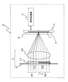
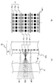
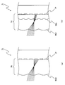
- FIG. 1 is a schematic diagram illustrating an imaging apparatus A according to the first embodiment.
- the image pickup apparatus A of the present embodiment includes a lens optical system L having V as an optical axis, an array-like optical element K arranged near the focal point of the lens optical system L, an image pickup element N, and a signal processing unit C. Prepare.
- the lens optical system L includes a diaphragm S on which light from a subject (not shown) enters, an optical element L1 on which light that has passed through the diaphragm S enters, and a lens L2 on which light that has passed through the optical element L1 enters. It is configured.
- the lens L2 may be composed of a single lens or a plurality of lenses. In FIG. 1, it is illustrated as a single sheet configuration.
- the optical element L1 is disposed in the vicinity of the stop.
- the optical element L1 has a first optical surface region D1 that transmits light in the first wavelength band and a second optical surface region D2 that transmits light in the second wavelength band.
- the first wavelength band and the second wavelength band are different from each other.
- the “wavelength band” in the “first wavelength band” and the “second wavelength band” is, for example, a continuous band that occupies 50% or more of the total amount of light transmitted through the region. A wavelength that is cut by 95% or more by passing is not included in the “wavelength band”.
- the two wavelength bands being different from each other means that at least one wavelength band includes a band that is not included in the other wavelength band. Therefore, some wavelength bands may overlap.
- the configurations in which the transmitted wavelength bands are different from each other include a configuration in which a filter using an organic material or a dielectric multilayer film is formed on the surface of the optical element L1 on the stop S side, a configuration in which an absorption filter is formed, and a staining system This is realized by a configuration in which the optical element L1 is dyed for each region by a filter.
- a color filter may be formed on one flat plate, or may be formed on a plurality of flat plates divided for each region.
- the light that has passed through the two optical surface regions D1 and D2 passes through the lens L2 and then enters the arrayed optical element K.
- the arrayed optical element K causes light that has passed through the optical surface region D1 to enter the pixel P1 in the image sensor N, and light that has passed through the optical surface region D2 to enter the pixel P2 in the image sensor N.
- the signal processing unit C generates image information corresponding to the first wavelength band from the pixel value obtained in the pixel P1, generates image information corresponding to the second wavelength band from the pixel value obtained in the pixel P2, Output.
- a light beam B1 is a light beam that passes through the optical surface region D1 on the optical element L1
- a light beam B2 is a light beam that passes through the optical surface region D2 on the optical element L1.
- the light beams B1 and B2 pass through the diaphragm S, the optical element L1, the lens L2, and the arrayed optical element K in this order, and reach the imaging surface Ni on the imaging element N.
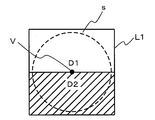
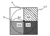
- FIG. 2 is a front view of the optical element L1 as viewed from the subject side.
- the optical surface regions D1 and D2 in the optical element L1 are formed by dividing the optical surface into two parts vertically in a plane perpendicular to the optical axis V with the optical axis V as the boundary center.
- the broken line s indicates the position of the diaphragm S.
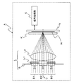
- FIG. 3 is a perspective view of the arrayed optical element K.
- FIG. 3 On the surface on the imaging element N side of the arrayed optical element K, a plurality of optical elements M1 elongated in the horizontal direction are arranged in the vertical direction.
- the cross section (longitudinal direction) of each optical element M1 has a curved shape protruding toward the image sensor N side.
- the arrayed optical element K has a lenticular lens configuration.
- the array-like optical element K is disposed in the vicinity of the focal point of the lens optical system L, and is disposed at a position away from the imaging surface Ni by a predetermined distance.
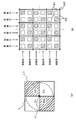
- FIG. 4A is an enlarged view of the arrayed optical element K and the image sensor N shown in FIG. 1, and FIG. 4B is a diagram illustrating the array of the optical element K and the pixels on the image sensor N. It is a figure which shows a positional relationship.
- the arrayed optical element K is arranged so that the surface on which the optical element M1 is formed faces the imaging surface Ni side.
- Pixels P are arranged in a matrix on the imaging surface Ni.
- the pixel P can be distinguished into a pixel P1 and a pixel P2.
- Each of the pixel P1 and the pixel P2 is arranged in a row in the horizontal direction (row direction). In the vertical direction (column direction), the pixels P1 and P2 are alternately arranged.
- the arrayed optical element K is arranged so that one of the optical elements M1 corresponds to two rows of pixels including one row of pixels P1 and one row of pixels P2 on the imaging surface Ni.
- a microlens Ms is provided so as to cover the surfaces of the pixels P1 and P2.
- the above configuration is realized by appropriately setting parameters such as the refractive index of the arrayed optical element K, the distance from the imaging surface Ni, and the radius of curvature of the surface of the optical element M1.
- the angle of the light beam at the focal point is determined by the position of the light beam passing through the stop and the angle with respect to the optical axis. Further, the array-like optical element has a function of distributing the emission direction according to the incident angle of the light beam. Therefore, by arranging the optical surface regions D1 and D2 in the vicinity of the stop, and arranging the arrayed optical element K in the vicinity of the focal point as described above, the light beams B1 and B2 that have passed through the optical surface regions are respectively pixelated. It can be separated into P1 and P2.
- the imaging optical system is an image side telecentric optical system
- the light rays passing through the stop are parallel, and therefore the angle of the light ray at the focal point is uniquely determined by the position of the light ray passing through the stop.
- the pixel P1 and the pixel P2 respectively generate image information corresponding to light in different wavelength bands. That is, the imaging apparatus A can acquire a plurality of pieces of image information formed by light having different wavelength bands with a single imaging optical system and with one imaging.
- the first optical surface region D1 is an optical filter having a characteristic of transmitting visible light as light in the first wavelength band and substantially blocking near-infrared light.
- the second optical surface region D2 is an optical filter having a characteristic of substantially blocking visible light and transmitting near-infrared light as light in the second wavelength band.
- the first optical surface region D1 is an optical filter having a characteristic of transmitting visible light as light in the first wavelength band and substantially blocking near ultraviolet light.
- the second optical surface region D2 is an optical filter having a characteristic of substantially blocking visible light and transmitting near-ultraviolet light as light in the second wavelength band.
- the first optical surface region D1 is an optical filter that transmits light of a predetermined wavelength bandwidth
- the second optical surface region D2 is a bandwidth narrower than the predetermined wavelength bandwidth. It is an optical filter which permeate
- the second wavelength band may or may not be included in the first wavelength band.
- one type of light source having spectral radiation characteristics including the first and second wavelength bands, or a plurality of types of spectral radiation characteristics corresponding to the first and second wavelength bands, respectively. It is preferable to provide a light source. In such applications, lesions can be easily distinguished by displaying images acquired in a wide band and images acquired in a narrow band in different colors.
- the pixel values in the y direction are missing every other pixel.
- the pixel value of the missing pixel may be generated by interpolating with the pixel value of the pixel adjacent in the y direction, or may be generated by adding the pixel values in the x direction by two pixels.
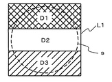
- the second embodiment is different from the first embodiment in that the area division of the optical element L1 is three.
- a detailed description of the same contents as in the first embodiment is omitted.
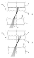
- FIG. 5 is a schematic diagram illustrating the imaging apparatus A according to the second embodiment.
- a light beam B1 is a light beam that passes through the optical surface region D1 on the optical element L1
- a light beam B2 is a light beam that passes through the optical surface region D2 on the optical element L1
- a light beam B3 is the optical element.
- the light beam passes through the optical surface region D3 on L1.
- the light beams B1, B2, and B3 pass through the stop S, the optical element L1, the lens L2, and the arrayed optical element K in this order, and reach the imaging surface Ni (shown in FIG. 7 and the like) on the imaging element N.
- FIG. 6 is a front view of the optical element L1 as seen from the subject side, and the optical surface regions D1, D2, and D3 are formed by being divided into three in the vertical direction within a plane perpendicular to the optical axis V. FIG. . Further, the wavelength bands of the light transmitted through each optical surface region are different from each other.
- FIG. 7A is an enlarged view of the arrayed optical element K and the image sensor N shown in FIG. 5, and FIG. 7B is a diagram illustrating the relationship between the arrayed optical element K and the pixels on the image sensor N. It is a figure which shows a positional relationship.
- the arrayed optical element K is arranged so that the surface on which the optical element M1 is formed faces the imaging surface Ni side.
- Pixels P are arranged in a matrix on the imaging surface Ni.
- the pixel P can be distinguished into a pixel P1, a pixel P2, and a pixel P3.
- Each of the pixel P1, the pixel P2, and the pixel P3 is arranged in a row in the horizontal direction (row direction). In the vertical direction (column direction), the pixels P1, P2, and P3 are repeatedly arranged.
- the array-like optical element K is arranged so that one of the optical elements M1 corresponds to three rows of pixels including one row of pixels P1, one row of pixels P2, and one row of pixels P3 on the imaging surface Ni. ing.
- a microlens Ms is provided so as to cover the surfaces of the pixels P1, P2, and P3.
- the above-described configuration is realized by appropriately setting parameters such as the refractive index of the arrayed optical element K, the distance from the imaging surface Ni, and the radius of curvature of the surface of the optical element M1.
- the pixel P1, the pixel P2, and the pixel P3 each generate image information corresponding to light in different wavelength bands. That is, the imaging apparatus A can acquire a plurality of pieces of image information formed by light having different wavelength bands with a single imaging optical system and with one imaging.
- the structure is such that images of two types of wavelength bands are acquired simultaneously, but in Embodiment 2, images of three types of wavelength bands can be acquired simultaneously.
- the first optical surface region D1 is a blue color filter that transmits light in a blue band and substantially blocks colors in a band other than blue.
- the second optical surface region D2 is a green color filter that transmits light in the green band and substantially blocks colors in bands other than green.
- the third optical surface region D3 is a red color filter that transmits light in the red band and substantially blocks colors in bands other than red.
- pixel values in the y direction are lost every two pixels.
- the pixel value of the missing pixel may be generated by interpolating with the pixel value of the pixel adjacent in the y direction, or may be generated by adding the pixel values in the x direction by three pixels.
- a configuration in which the aspect ratio of each pixel of the image sensor in the x direction and the y direction is 3: 1 may be employed. With such a configuration, the above-described interpolation processing and addition processing are not necessary.
- the third embodiment is different from the first embodiment in that the area division of the optical element L1 in FIG. 1 is changed to four and the array-like optical element is replaced with a microlens from the lenticular.
- a detailed description of the same contents as in the first embodiment is omitted.
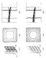
- FIG. 8 is a front view of the optical element L1 as viewed from the subject side.
- the optical surface regions D1, D2, D3, and D4 are vertically and horizontally 4 in a plane perpendicular to the optical axis V with the optical axis V as a center. It is formed by being divided. Further, the wavelength bands of the light transmitted through each optical surface region are different from each other.
- FIG. 9 is a perspective view of the arrayed optical element K.
- FIG. 9 On the surface of the arrayed optical element K on the imaging element N side, optical elements M2 are arranged in a grid pattern. Each optical element M2 has a curved cross-section (vertical and horizontal cross-sections), and each optical element M2 protrudes toward the image sensor N.
- the optical element M2 is a microlens
- the arrayed optical element K is a microlens array.
- FIG. 10A is an enlarged view showing the arrayed optical element K and the image sensor N
- FIG. 10B shows the positional relationship between the arrayed optical element K and the pixels on the image sensor N.
- the arrayed optical element K is arranged so that the surface on which the optical element M2 is formed faces the imaging surface Ni side.
- Pixels P are arranged in a matrix on the imaging surface Ni.
- the pixel P can be distinguished into a pixel P1, a pixel P2, a pixel P3, and a pixel P4.
- the arrayed optical element K is disposed in the vicinity of the focal point of the lens optical system L, and is disposed at a position away from the imaging surface Ni by a predetermined distance.
- a microlens Ms is provided on the imaging surface Ni so as to cover the surfaces of the pixels P1, P2, P3, and P4.
- the arrayed optical element K is arranged so that the surface on which the optical element M2 is formed faces the imaging surface Ni side.
- the arrayed optical element K is arranged so that one of the optical elements M2 corresponds to four pixels of pixels P1 to P4 in 2 rows and 2 columns on the imaging surface Ni.
- the above-described configuration is realized by appropriately setting parameters such as the refractive index of the arrayed optical element K, the distance from the imaging surface Ni, and the radius of curvature of the surface of the optical element M1.
- the pixel P1, the pixel P2, the pixel P3, and the pixel P4 each generate image information corresponding to light in different wavelength bands. That is, the imaging apparatus A can acquire a plurality of pieces of image information formed by light of different wavelength bands with a single imaging optical system and with one imaging.
- the structure is such that images of two types and three types of wavelength bands are acquired simultaneously, but in Embodiment 3, images of four types of wavelength bands are acquired simultaneously. Can do.
- visible light including blue, green, and red is substantially blocked, and near-infrared light that transmits near-infrared light is transmitted.
- the configuration includes an infrared light filter.
- an imaging device for day and night and an imaging device for biometric authentication can be realized.
- visible light including the blue, green, and red is substantially blocked and near-ultraviolet light is transmitted.
- the configuration includes an ultraviolet light filter.
- the imaging device which visualizes the state of skin such as a stain caused by near ultraviolet rays can be realized.
- it is preferable to include a light source having spectral radiation characteristics including a near ultraviolet light band.
- the filter is configured to transmit only the wavelength band.
- the narrow band described above may or may not be included in any of the blue, green, and red color filters.
- the light source provided with the white light source and the light source which has the spectral radiation characteristic containing the said narrow band may be sufficient.
- the pixel values in the x direction and the y direction are missing every other pixel. Therefore, the pixel values of the missing pixels may be generated by interpolating with the pixel values of the pixels adjacent in the x direction and the y direction, respectively.
- two regions facing each other across the optical axis among the four divided regions may be the same green color filter.
- each of the first optical surface region D1 and the second optical surface region D2 is separated from the optical axis, and the arrayed optical element is changed from a lenticular to a microlens. This is different from the first embodiment in the point of replacement. Here, a detailed description of the same contents as in the first embodiment is omitted.
- FIG. 11A is a front view of the optical element L1 as viewed from the subject side.
- Each of the optical surface regions D1 and D2 has an axially symmetric direction about the optical axis V so that the center of gravity is the optical axis position.
- FIG. 11B is a diagram showing the positional relationship between the arrayed optical element K and the pixels on the image sensor N.
- the odd-numbered row odd-numbered column and the even-numbered row even-numbered column are added to the first wavelength band. Generate a corresponding image.
- the even-numbered odd-numbered column and the odd-numbered even-numbered column are added to generate an image corresponding to the second wavelength band.
- the first optical surface region D1 and the second optical surface region D2 are regions formed by dividing the optical element L1 into two vertically in a plane perpendicular to the optical axis. For this reason, the center of gravity of the spot on the image plane of the light passing through each optical surface region may change depending on the subject distance, and parallax may occur.
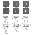
- FIG. 12 is a diagram for explaining a light ray diagram for each subject distance in the first embodiment and a change of a point image and its center of gravity.
- 12 (a1), (b1), and (c1) are ray diagrams for each subject distance.
- 12 (a1) shows the case where the object point O is the farthest distance from the optical system
- FIG. 12 (c1) shows the case where the object point O is the closest
- FIG. 12 (b1) It is a light ray figure in case the object point O exists in the distance between (c1).
- the same symbols are used for the same configurations as in FIG. FIGS.
- Each point image is a pixel value obtained by missing image information (a2, b2, c2) extracted for every odd column and pixel information (a3, b3, c3) extracted for every even column every other pixel in the Y direction.
- pixel information a3, b3, c3 extracted for every even column every other pixel in the Y direction.
- the optical surface regions D1 and D2 are arranged separately in the axially symmetric direction around the optical axis so that the center of gravity is the optical axis position.
- the center of gravity of the point image formed by the light passing through the optical surface regions D1 and D2 also exists at the optical axis position. For this reason, even if the subject distance changes, the distance d between the centers of gravity of the point images does not change.
- FIG. 13 is a diagram for explaining a point image and its center of gravity for each subject distance.
- (a1) and (a2), (b1) and (b2), and (c1) and (c2) are point images (shown as semicircles) imaged through a microlens and their centroids (black dots). These correspond to the subject distances of (a1), (b1), and (c1) in FIG.
- Each point image includes image information (a1, b1, c1) obtained by adding odd rows and odd columns and even rows and even columns, and image information (a2, b2, c2) obtained by adding even rows and odd columns and odd rows and even columns.
- image information (a1, b1, c1) obtained by adding odd rows and odd columns and even rows and even columns
- image information (a2, b2, c2) obtained by adding even rows and odd columns and odd rows and even columns.
- each of the optical surface regions D1 and D2 is arranged in the axially symmetric direction with the optical axis as the center so that the center of gravity is located at the optical axis position. It is possible to prevent parallax from occurring between the acquired images even if changes.
- the fifth embodiment is premised on the configuration having the two optical surface regions D1 and D2 as in the first embodiment, and the lens L2 is a lens having axial chromatic aberration.
- 2 having different optical powers in a plane perpendicular to the optical axis in the vicinity of the stop so that the in-focus positions of the light beams transmitted through the optical surface regions D1 and D2 are substantially equal.
- a detailed description of the same contents as in the first embodiment is omitted.
- one of the two regions having different optical powers transmits the light transmitted through the first optical surface region D1.
- the other region transmits light that passes through the second optical surface region D2.
- Two regions having different optical powers from the optical surface regions D1 and D2 may be formed in the same element, or may be formed in different elements.
- FIG. 14A is a diagram schematically showing a ray diagram when the lens L2 is a lens having axial chromatic aberration due to the wavelength dispersion characteristic of the refractive index as in the case of the single lens in the first embodiment.
- a filter that transmits light in the first wavelength band is formed in the first optical surface region D1, and relative to the second optical surface region D2 than in the first wavelength band.
- a filter that transmits light having a long second wavelength band is formed.
- the lens L2 is a lens having axial chromatic aberration due to the wavelength dispersion characteristic of the refractive index, such as a single lens, and therefore, the longer the wavelength, the more the lens L2 is focused. Therefore, as shown in FIG. 14A, when the light beam that has passed through the optical surface region D1 is set to be focused on the imaging surface Ni, the light beam that has passed through the optical surface region D2 is focused on the imaging surface Ni. It will be in a state that cannot be burned.
- FIG. 14B is a diagram schematically showing a light ray diagram of the imaging apparatus of the fifth embodiment.
- the light beam in the wavelength band in the second spectral transmittance characteristic is focused on the imaging surface on the second optical surface region D2 of the optical element L1.
- a lens surface with an appropriate optical power is formed.
- the light beam that has passed through the first optical surface region D1 and the light beam that has passed through the second optical surface region D2 are both focused on the imaging surface Ni.
- the first optical surface region D1 and the second optical surface region D2 have different optical powers, so that the first optical surface region D1 and the second optical surface region D2 have different optical powers.
- the focus position of the light transmitted through the first optical surface region D1 and the focus position of the light transmitted through the second optical surface region D2 are closer.
- the optical axis V ′ of the optical surface on the stop S side of the optical surface region D2 of the optical element L1 has an eccentricity unlike the optical axis V of the lens optical system, but its optical power is Since it is extremely small compared to the optical power of the lens L2, there is little deterioration in imaging performance.
- FIG. 15 (a) and 15 (b) are perspective views of the optical element L1 shown in FIG. 14 (b).
- a filter having the first spectral transmittance characteristic is formed on the first optical surface region D1 which is a plane
- the second spectral transmittance is formed on the second optical surface region D2 which is a lens surface.
- a filter having characteristics is formed.
- the lens surface is formed over the entire region obtained by dividing the optical element L1 into two parts. For this reason, a step is generated between the first optical surface region which is a flat surface and the second optical surface region D2 which is a lens surface.
- the diaphragm S has a light shielding region as shown in FIGS. 16 (a) and 16 (b).
- a lens surface is formed in a part of a region formed by dividing the optical element L1 into two to form an optical surface region D2.
- This configuration requires a configuration in which a light shielding region as shown in FIG. 16C is provided so as to correspond to the optical surface regions D1 and D2.
- FIG. 17 (a) and 17 (b) are diagrams showing another form of the fifth embodiment.
- the optical axis V ′ of the optical surface on the stop S side of the optical surface region D2 of the optical element L1 is different from the optical axis V of the lens optical system, but in FIG.
- the optical axis of the optical surface on the stop S side of the optical surface region D2 is the same as the optical axis of the lens L2.
- FIG. 18 is a perspective view of the optical element L1 shown in FIG. With such a configuration, the decentering of the optical axis of the lens surface of the optical surface region D2 of the optical element L1 is eliminated, so that deterioration in imaging performance due to decentering can be eliminated.
- FIG. 17B is an example in which the lens provided on the optical element L1 is configured separately from FIG. 17A.
- an optical element L1 in which filters having different spectral transmittance characteristics are formed is disposed on the subject side near the diaphragm, and an optical element L1 ′ is disposed on the object side near the diaphragm.
- Each of the optical elements L1 and L1 ′ has a first optical surface region D1 and a second optical surface region D2.
- the second optical surface region D2 in the optical element L1 ′ has a lens surface.
- the element forming the filter and the element forming the lens may be separate. Further, the positions of L1 and L1 ′ may be switched with respect to the stop.
- the lens L2 is a single lens that is not corrected for axial chromatic aberration, 2 having different optical powers in a plane perpendicular to the optical axis. By providing two regions, axial chromatic aberration can be reduced.
- the sixth embodiment is premised on a configuration having three optical surface regions D1, D2, and D3 as in the second embodiment, and the lens L2 is a lens having axial chromatic aberration.
- 3 having different optical powers in a plane perpendicular to the optical axis in the vicinity of the stop so that the in-focus positions of the light beams transmitted through the optical surface regions D1 and D2 are substantially equal.
- a detailed description of the same contents as in the fifth embodiment is omitted.
- the diaphragm S has the configuration shown in FIGS. 20 (a), (b), and (c), respectively.
- three lenses having different optical powers in a plane perpendicular to the optical axis are used even when a lens whose axial chromatic aberration is not corrected and corrected, such as a single lens, is used.
- a lens whose axial chromatic aberration is not corrected and corrected such as a single lens
- the present seventh embodiment is based on the premise that, as in the third embodiment, there are four optical surface regions D1, D2, D3, and D4, and the lens L2 is a lens having axial chromatic aberration. To do.
- a detailed description of the same contents as in the fifth embodiment is omitted.
- FIG 21 (a), (b) and (c) are perspective views of the optical element L1 when each optical surface area is divided into four in the seventh embodiment.
- the diaphragm S has a configuration shown in FIGS. 22 (a), (b), and (c), respectively.
- the seventh embodiment four lenses having different optical powers in a plane perpendicular to the optical axis are used even when a lens whose axial chromatic aberration is not corrected and corrected, such as a single lens, is used.
- a lens whose axial chromatic aberration is not corrected and corrected such as a single lens
- the eighth embodiment differs from the first to seventh embodiments in that a lenticular lens and a microlens array are formed on the imaging surface.
- a lenticular lens and a microlens array are formed on the imaging surface.
- FIG. 23 (a) and 23 (b) are diagrams showing the arrayed optical element K and the imaging element N in an enlarged manner.
- a lenticular lens (or microlens array) Md is formed on the imaging surface Ni of the imaging element N.
- Pixels P are arranged in a matrix on the imaging surface Ni, as in the first embodiment.
- One lenticular lens optical element or one microlens corresponds to the plurality of pixels P.
- the light beams that have passed through different regions on the optical element L1 can be guided to different pixels.
- FIG. 23B is a diagram showing a modification of the present embodiment. In the configuration shown in FIG.
- a microlens Ms is formed on the imaging surface Ni so as to cover the pixel P, and an arrayed optical element is stacked on the surface of the microlens Ms.
- the light collection efficiency can be increased as compared with the configuration in FIG.
- the array-like optical element is separated from the image sensor as in the first to seventh embodiments, it is difficult to align the array-like optical element and the image sensor.
- the array-like optical element is difficult to align.
- the lens L2 has a single configuration, it may be a lens having a plurality of groups or a plurality of configurations.
- the optical surface area is arranged on the object side surface of the optical element L1
- the optical surface area may be arranged on the image side surface of the optical element L1.
- the optical element L1 is disposed closer to the subject with respect to the position of the diaphragm because the arrangement is closer to the diaphragm.
- the optical element L1 is disposed on the image side with respect to the position of the stop, but may be disposed on the subject side with respect to the position of the stop. In this case, it is preferable that the optical surface area is disposed on the image side of the optical element L1 because it is closer to the stop.
- the lens surface provided in the optical element L1 or an element different from the optical element L1 is disposed on the object side surface of the element, but is disposed on the image side surface of the element. May be.
- Embodiments 1 to 8 only one color filter is disposed in each optical region in the direction of the optical axis, but a plurality of color filters may be stacked.
- a dielectric multilayer film filter and an absorption type filter having different spectral transmittance characteristics may be stacked, and a dielectric multilayer film may be formed on the absorption type filter.
- an image-side non-telecentric optical system may be applied, or an image-side telecentric optical system may be applied.
- Many lenses used in image pickup devices such as cameras have non-telecentric optical systems on the image side.
- the image-side non-telecentric optical system is applied to the lens optical system L according to the present invention, the principal ray is incident on the arrayed optical element K obliquely when the angle of view changes.
- FIG. 24A is an enlarged view showing the vicinity of the imaging unit outside the optical axis. In FIG. 24A, only the light beam that passes through one optical surface region of the light that passes through the arrayed optical element K is shown. As shown in FIG.
- the lens optical system L when the lens optical system L is an image-side non-telecentric optical system, light leaks to adjacent pixels and crosstalk tends to occur, but as shown in FIG.
- the offset amount ⁇ may be set according to the incident angle of the light beam on the imaging surface.
- an image side telecentric optical system may be applied to the lens optical system L of the embodiment of the present invention.
- the chief ray is incident on the arrayed optical element K at a value close to 0 degrees, so that crosstalk can be reduced over the entire imaging region. .
- the arrayed optical element K is a microlens array, but each optical element of the microlens has a rotationally symmetric shape with respect to the optical axis of each macrolens.
- a method of manufacturing the microlens there is a method of patterning a resist into a rectangle and forming a lens curved surface by heat treatment.
- a perspective view of such a microlens is as shown in FIG.
- the contour lines of the microlens in FIG. 25 (a1) are as shown in FIG. 25 (a2), so that the curvature radii in the vertical and horizontal directions are different from those in the oblique direction.
- FIG. 25 (a3) shows the result of ray tracing simulation when the microlens shown in FIGS. 25 (a1) and (a2) is applied to the arrayed optical element of the present invention.
- FIG. 25 (a3) only the light beam passing through one optical surface region of the light passing through the arrayed optical element K is shown. Light leaks and crosstalk occurs.
- a perspective view of a rotationally symmetric microlens is as shown in FIG.
- the contour lines of the microlens in FIG. 25 (b1) are as shown in FIG. 25 (b2), and the curvature radii in the vertical and horizontal directions and the oblique direction are equal.
- Such a rotationally symmetric microlens can be formed by thermal imprinting or UV imprinting.
- FIG. 25 (b3) shows a result of ray tracing simulation when the microlens shown in FIGS. 25 (b1) and (b2) is applied to the arrayed optical element of the present invention.
- FIG. 25 (b3) only the light beam passing through one optical surface region among the light passing through the arrayed optical element K is shown, but the crosstalk as shown in FIG. 25 (a3) does not occur. I understand that.
- crosstalk can be reduced, so that deterioration of color purity can be suppressed.
- the image sensor used in the first to eighth embodiments may be either a monochrome image sensor or a color image sensor.
- the width of the wavelength band of the light transmitted through at least one region of the optical element L1 is the width of the wavelength band of the color filter on the pixel to which the light beam passing through the region reaches.
- a narrower configuration may be used. Since the image pickup element uses a color image pickup element, it is not necessary to provide a color filter other than the at least one region of the optical element L1. With such a configuration, it is possible to acquire narrow-band image information, and it is possible to attenuate a wavelength band component caused by crosstalk due to the effect of the spectral transmittance characteristics of the color imaging element. Further, since it is not necessary to provide a color filter on the optical element L1 other than the at least one region, the cost can be reduced.
- Embodiments 1 to 8 are imaging devices including a signal processing unit C.
- the imaging device of the present invention may not include these signal processing units.
- the processing performed by the signal processing unit C may be performed using a PC or the like outside the imaging apparatus.
- the present invention can also be realized by a system including an imaging device including the lens optical system L, the arrayed optical element K, and the imaging device N, and an external signal processing device.
- the imaging device according to the present invention is useful as an imaging device such as a digital still camera or a digital video camera.
- the present invention can also be applied to medical cameras such as in-vehicle cameras, security cameras, endoscopes and capsule endoscopes, biometric authentication cameras, microscopes, and astronomical telescopes.
Abstract
Description
図1は、実施の形態1の撮像装置Aを示す模式図である。本実施形態の撮像装置Aは、Vを光軸とするレンズ光学系Lと、レンズ光学系Lの焦点近傍に配置されたアレイ状光学素子Kと、撮像素子Nと、信号処理部Cとを備える。 (Embodiment 1)
FIG. 1 is a schematic diagram illustrating an imaging apparatus A according to the first embodiment. The image pickup apparatus A of the present embodiment includes a lens optical system L having V as an optical axis, an array-like optical element K arranged near the focal point of the lens optical system L, an image pickup element N, and a signal processing unit C. Prepare.
本実施の形態2は、光学素子L1の領域分割を3つにした点で、実施の形態1と異なっている。ここでは、実施の形態1と同様の内容についての詳細な説明は省略する。 (Embodiment 2)
The second embodiment is different from the first embodiment in that the area division of the optical element L1 is three. Here, a detailed description of the same contents as in the first embodiment is omitted.
本実施の形態3は、図1の光学素子L1の領域分割を4つにした点と、アレイ状光学素子をレンチキュラからマイクロレンズに置き換えた点で、実施の形態1と異なっている。ここでは、実施の形態1と同様の内容についての詳細な説明は省略する。 (Embodiment 3)
The third embodiment is different from the first embodiment in that the area division of the optical element L1 in FIG. 1 is changed to four and the array-like optical element is replaced with a microlens from the lenticular. Here, a detailed description of the same contents as in the first embodiment is omitted.
本実施の形態4は、第1の光学面領域D1及び第2の光学面領域D2のそれぞれが、光軸を挟んで分離して配置された点と、アレイ状光学素子をレンチキュラからマイクロレンズに置き換えた点で、実施の形態1と異なっている。ここでは、実施の形態1と同様の内容についての詳細な説明は省略する。 (Embodiment 4)
In the fourth embodiment, each of the first optical surface region D1 and the second optical surface region D2 is separated from the optical axis, and the arrayed optical element is changed from a lenticular to a microlens. This is different from the first embodiment in the point of replacement. Here, a detailed description of the same contents as in the first embodiment is omitted.
本実施の形態5は、実施の形態1のように2つの光学面領域D1及びD2を有する構成であって、さらにレンズL2が軸上色収差を有するレンズである場合を前提とする。このような構成の場合に、光学面領域D1及びD2を透過した光線の合焦位置が実質的に等しくなるように、絞り近傍の光軸と垂直な面内で、互いに異なる光学パワーを有する2つの領域を有している。この点で実施の形態1と異なっている。ここでは、実施の形態1と同様の内容についての詳細な説明は省略する。 (Embodiment 5)
The fifth embodiment is premised on the configuration having the two optical surface regions D1 and D2 as in the first embodiment, and the lens L2 is a lens having axial chromatic aberration. In such a configuration, 2 having different optical powers in a plane perpendicular to the optical axis in the vicinity of the stop so that the in-focus positions of the light beams transmitted through the optical surface regions D1 and D2 are substantially equal. Has two areas. This is different from the first embodiment. Here, a detailed description of the same contents as in the first embodiment is omitted.
本実施の形態6は、実施の形態2のように、3つの光学面領域D1、D2及びD3を有する構成であって、さらにレンズL2が軸上色収差を有するレンズである場合を前提とする。このような構成の場合に、光学面領域D1及びD2を透過した光線の合焦位置が実質的に等しくなるように、絞り近傍の光軸と垂直な面内で、互いに異なる光学パワーを有する3つの領域を有している。この点で、実施の形態5と異なっている。ここでは、実施の形態5と同様の内容についての詳細な説明は省略する。 (Embodiment 6)
The sixth embodiment is premised on a configuration having three optical surface regions D1, D2, and D3 as in the second embodiment, and the lens L2 is a lens having axial chromatic aberration. In the case of such a configuration, 3 having different optical powers in a plane perpendicular to the optical axis in the vicinity of the stop so that the in-focus positions of the light beams transmitted through the optical surface regions D1 and D2 are substantially equal. Has two areas. This is different from the fifth embodiment. Here, a detailed description of the same contents as in the fifth embodiment is omitted.
本実施の形態7は、実施の形態3のように、4つの光学面領域D1、D2、D3及びD4を有する構成であって、さらにレンズL2が軸上色収差を有するレンズである場合を前提とする。このような構成の場合に、光学面領域D1及びD2を透過した光線の合焦位置が実質的に等しくなるように、絞り近傍の光軸と垂直な面内で、互いに異なる光学パワーを有する4つの領域を有している。この点で、実施の形態5と異なっている。ここでは、実施の形態5と同様の内容についての詳細な説明は省略する。 (Embodiment 7)
The present seventh embodiment is based on the premise that, as in the third embodiment, there are four optical surface regions D1, D2, D3, and D4, and the lens L2 is a lens having axial chromatic aberration. To do. In the case of such a configuration, 4 having different optical powers in a plane perpendicular to the optical axis in the vicinity of the stop so that the in-focus positions of the light beams transmitted through the optical surface regions D1 and D2 are substantially equal. Has two areas. This is different from the fifth embodiment. Here, a detailed description of the same contents as in the fifth embodiment is omitted.
本実施の形態8は、レンチキュラレンズやマイクロレンズアレイを撮像面上に形成したという点で、実施の形態1~7と異なる。ここでは、本実施形態において実施の形態1~7と同様の内容についての詳細な説明は省略する。 (Embodiment 8)
The eighth embodiment differs from the first to seventh embodiments in that a lenticular lens and a microlens array are formed on the imaging surface. Here, detailed description of the same contents as in the first to seventh embodiments is omitted in this embodiment.
実施の形態1から8では、各光学面領域の分割数が2分割、3分割、4分割の構成について説明したが、より多くの分割数であってもよい。 (Other embodiments)
In the first to eighth embodiments, the configuration in which the number of divisions of each optical surface region is two divisions, three divisions, and four divisions has been described, but a larger number of divisions may be used.
L レンズ光学系
L1,L1' 光学素子
L2 レンズ
D1,D2,D3,D4 光学面領域
S 絞り
K アレイ状光学素子
N 撮像素子
Ni 撮像面
Ms,Md 撮像素子上のマイクロレンズ
M1 アレイ状光学素子の光学要素(レンチキュラ)
M2 アレイ状光学素子の光学要素(マイクロレンズ)
P1,P2,P3,P4,P 撮像素子上の画素
C 信号処理部 A Imaging device L Lens optical system L1, L1 ′ Optical element L2 Lens D1, D2, D3, D4 Optical surface area S Aperture K Array optical element N Imaging element Ni Imaging surface Ms, Md Micro lens on imaging element M1 Array Optical element of optical element (lenticular)
M2 Optical element of array optical element (micro lens)
P1, P2, P3, P4, P Pixels on the image sensor C Signal processing unit
Claims (22)
- レンズ及び絞りを有するレンズ光学系と、
前記レンズ光学系を透過した光が入射する複数の第1の画素と複数の第2の画素とを少なくとも有する撮像素子と、
前記レンズ光学系と前記撮像素子との間に配置されたアレイ状光学素子とを備え、
前記レンズ光学系は、光軸と垂直な面内に複数の領域をさらに有し、
前記複数の領域は、第1の波長帯域の光を透過する第1の領域と、前記第1の波長帯域と異なる第2の波長帯域の光を透過する第2の領域とを含み、
前記アレイ状光学素子は、前記第1の領域を透過した光を前記複数の第1の画素に入射させ、前記第2の領域を透過した光を前記複数の第2の画素に入射させる、撮像装置。 A lens optical system having a lens and a diaphragm;
An imaging device having at least a plurality of first pixels and a plurality of second pixels on which light transmitted through the lens optical system is incident;
An arrayed optical element disposed between the lens optical system and the imaging element;
The lens optical system further includes a plurality of regions in a plane perpendicular to the optical axis,
The plurality of regions include a first region that transmits light in a first wavelength band, and a second region that transmits light in a second wavelength band different from the first wavelength band,
The array-like optical element causes the light transmitted through the first region to enter the plurality of first pixels, and causes the light transmitted through the second region to enter the plurality of second pixels. apparatus. - 前記複数の領域は、前記絞り近傍に配置されている、請求項1に記載の撮像装置。 The imaging device according to claim 1, wherein the plurality of regions are arranged in the vicinity of the diaphragm.
- 前記レンズ光学系の前記複数の領域は、前記第1、第2の領域以外の少なくとも第3の領域をさらに含み、
前記第3の領域は、前記第1の波長帯域および前記第2の波長帯域と異なる第3の波長帯域の光を透過し、
前記アレイ状光学素子は、前記第3の領域を透過した光を、前記複数の第1、第2の画素以外の第3の画素に入射させる、請求項1または2に記載の撮像装置。 The plurality of regions of the lens optical system further include at least a third region other than the first and second regions,
The third region transmits light in a third wavelength band different from the first wavelength band and the second wavelength band,
The imaging apparatus according to claim 1, wherein the arrayed optical element causes light transmitted through the third region to enter a third pixel other than the plurality of first and second pixels. - 前記レンズ光学系の前記複数の領域は、前記第1、第2及び第3の領域以外の第4の領域をさらに含み、前記第4の領域は、前記第1、第2および第3の波長帯域と異なる第4の波長帯域の光を透過し、
前記アレイ状光学素子は、前記第4の領域を透過した光を、前記複数の第1、第2及び第3の画素以外の第4の画素に入射させる、請求項3に記載の撮像装置。 The plurality of regions of the lens optical system further include a fourth region other than the first, second, and third regions, and the fourth region includes the first, second, and third wavelengths. Transmits light in a fourth wavelength band different from the band,
The imaging apparatus according to claim 3, wherein the arrayed optical element causes light transmitted through the fourth region to enter a fourth pixel other than the plurality of first, second, and third pixels. - 前記レンズ光学系の前記第1および第2の領域のそれぞれは、光軸を挟んで互いに分離された複数の領域から構成されている、請求項1から4のいずれかに記載の撮像装置。 The imaging apparatus according to any one of claims 1 to 4, wherein each of the first and second regions of the lens optical system includes a plurality of regions separated from each other with an optical axis interposed therebetween.
- 前記第1の波長帯域の光は近赤外光であり、前記第2の波長帯域の光は可視光である、請求項1から5のいずれかに記載の撮像装置。 6. The imaging device according to claim 1, wherein the light in the first wavelength band is near infrared light, and the light in the second wavelength band is visible light.
- 前記第1の波長帯域の光は近紫外光であり、前記第2の波長帯域の光は可視光である、請求項1から5のいずれかに記載の撮像装置。 6. The imaging device according to claim 1, wherein the light in the first wavelength band is near ultraviolet light, and the light in the second wavelength band is visible light.
- 前記第1の波長帯域の幅よりも、前記第2の波長帯域の幅が狭い請求項1から5のいずれかに記載の撮像装置。 6. The imaging apparatus according to claim 1, wherein a width of the second wavelength band is narrower than a width of the first wavelength band.
- 前記第1の領域および前記第2の領域は、前記レンズ光学系の光軸を境界中心として、前記光軸に垂直な面内で分割された領域である、請求項1から4のいずれかに記載の撮像装置。 5. The device according to claim 1, wherein the first region and the second region are regions divided in a plane perpendicular to the optical axis with the optical axis of the lens optical system as a boundary center. 6. The imaging device described.
- 前記第1の領域および前記第2の領域は互いに異なる光学パワーを有し、
前記第1の領域および前記第2の領域が互いに等しい光学パワーを有する場合と比較して、前記第1の領域を透過した光の合焦位置と前記第2の領域を透過した光の合焦位置とが近い、請求項1から9のいずれかに記載の撮像装置。 The first region and the second region have different optical powers;
Compared with the case where the first region and the second region have the same optical power, the focus position of the light transmitted through the first region and the focus of the light transmitted through the second region are compared. The imaging apparatus according to claim 1, wherein the imaging apparatus is close in position. - 前記レンズ光学系は像側非テレセントリック光学系であって、
前記レンズ光学系の光軸外において前記アレイ状光学素子の配列を前記撮像素子の画素の配列に対してオフセットさせている、請求項1から10のいずれかに記載の撮像装置。 The lens optical system is an image-side non-telecentric optical system,
The imaging apparatus according to claim 1, wherein an array of the arrayed optical elements is offset from an array of pixels of the imaging element outside the optical axis of the lens optical system. - 前記レンズ光学系が像側テレセントリック光学系である、請求項1から10のいずれかに記載の撮像装置。 The imaging apparatus according to claim 1, wherein the lens optical system is an image side telecentric optical system.
- 前記アレイ状光学素子はレンチキュラレンズである、請求項1から12のいずれかに記載の撮像装置。 The imaging apparatus according to any one of claims 1 to 12, wherein the arrayed optical element is a lenticular lens.
- 前記アレイ状光学素子はマイクロレンズアレイである、請求項1から12のいずれかに記載の撮像装置。 The imaging apparatus according to any one of claims 1 to 12, wherein the arrayed optical element is a microlens array.
- 前記マイクロレンズアレイの各光学要素の形状が回転対称形状である、請求項14に記載の撮像装置。 The imaging device according to claim 14, wherein the shape of each optical element of the microlens array is a rotationally symmetric shape.
- 前記アレイ状光学素子は前記撮像素子上に形成されている、請求項1から15のいずれかに記載の撮像装置。 The imaging device according to any one of claims 1 to 15, wherein the arrayed optical element is formed on the imaging element.
- 前記アレイ状光学素子と前記撮像素子との間に設けられたマイクロレンズをさらに備え、
前記アレイ状光学素子は、前記マイクロレンズを介して前記撮像素子上に形成されている、請求項16に記載の撮像装置。 A microlens provided between the arrayed optical element and the imaging element;
The imaging device according to claim 16, wherein the arrayed optical element is formed on the imaging element via the microlens. - 前記第1の領域および前記第2の領域の境界部に対応する位置に遮光領域をさらに備える請求項1から17のいずれかに記載の撮像装置。 The imaging device according to any one of claims 1 to 17, further comprising a light-shielding region at a position corresponding to a boundary portion between the first region and the second region.
- 前記撮像素子は、各画素上にカラーフィルタの形成されたカラー撮像素子であって、
前記複数の領域のうち少なくとも1つの領域の波長帯域の幅が、該領域を透過した光束が到達する前記カラー撮像素子上のカラーフィルタの波長帯域の幅よりも狭い請求項1から18のいずれかに記載の撮像装置。 The image sensor is a color image sensor in which a color filter is formed on each pixel,
The width of the wavelength band of at least one area of the plurality of areas is narrower than the width of the wavelength band of the color filter on the color image sensor on which the light beam transmitted through the area reaches. The imaging device described in 1. - 信号処理部をさらに備え、
前記信号処理部は、前記複数の第1の画素において得られた画素値から第1の波長帯域に対応する第1の画像情報を生成し、前記複数の第2の画素において得られた画素値から第2の波長帯域に対応する第2の画像情報を生成する、請求項1から19のいずれかに記載の撮像装置。 A signal processing unit,
The signal processing unit generates first image information corresponding to a first wavelength band from pixel values obtained in the plurality of first pixels, and pixel values obtained in the plurality of second pixels. The imaging device according to any one of claims 1 to 19, wherein second image information corresponding to the second wavelength band is generated. - 請求項1から19のいずれかに記載の撮像装置と、
前記撮像装置における前記複数の第1の画素において得られた画素値から第1の波長帯域に対応する第1の画像情報を生成し、前記複数の第2の画素において得られた画素値から第2の波長帯域に対応する第2の画像情報を生成する信号処理装置とを備える撮像システム。 An imaging device according to any one of claims 1 to 19,
First image information corresponding to a first wavelength band is generated from pixel values obtained at the plurality of first pixels in the imaging device, and first pixel information obtained from the plurality of second pixels is And a signal processing device that generates second image information corresponding to the second wavelength band. - 第1の波長帯域の光を透過する第1の領域と、前記第1の波長帯域とは異なる第2の波長帯域の光を透過する第2の領域とを少なくとも有するレンズ光学系と、
前記レンズ光学系を透過した光が入射する複数の第1の画素と複数の第2の画素とを少なくとも有する撮像素子と、
前記レンズ光学系と前記撮像素子との間に配置されたアレイ状光学素子とを備える撮像装置を用い、
前記アレイ状光学素子によって、前記第1の領域を透過した光を前記複数の第1の画素に入射させ、前記第2の領域を透過した光を前記複数の第2の画素に入射させ、
前記複数の第1の画素において得られた画素値から第1の波長帯域に対応する第1の画像および前記複数の第2の画素において得られた画素値から第2の波長帯域に対応する第2の画像情報を生成する、撮像方法。 A lens optical system having at least a first region that transmits light in a first wavelength band and a second region that transmits light in a second wavelength band different from the first wavelength band;
An imaging device having at least a plurality of first pixels and a plurality of second pixels on which light transmitted through the lens optical system is incident;
Using an imaging device comprising an array-like optical element disposed between the lens optical system and the imaging element,
By the arrayed optical element, the light transmitted through the first region is incident on the plurality of first pixels, and the light transmitted through the second region is incident on the plurality of second pixels.
The first image corresponding to the first wavelength band from the pixel values obtained in the plurality of first pixels and the first corresponding to the second wavelength band from the pixel values obtained in the plurality of second pixels. The imaging method which produces | generates 2 image information.
Priority Applications (5)
| Application Number | Priority Date | Filing Date | Title |
|---|---|---|---|
| US13/519,627 US8717483B2 (en) | 2011-04-22 | 2011-10-31 | Imaging device, imaging system, and imaging method |
| EP11852202.8A EP2536153B1 (en) | 2011-04-22 | 2011-10-31 | Image capture device, image capture system, and image capture method |
| JP2012508278A JP5001471B1 (en) | 2011-04-22 | 2011-10-31 | Imaging apparatus, imaging system, and imaging method |
| CN201180005162.9A CN102907102B (en) | 2011-04-22 | 2011-10-31 | Image capture device, imgae capture system, and image capture method |
| US14/189,190 US8854525B2 (en) | 2011-04-22 | 2014-02-25 | Imaging device, imaging system, and imaging method |
Applications Claiming Priority (2)
| Application Number | Priority Date | Filing Date | Title |
|---|---|---|---|
| JP2011-095742 | 2011-04-22 | ||
| JP2011095742 | 2011-04-22 |
Related Child Applications (2)
| Application Number | Title | Priority Date | Filing Date |
|---|---|---|---|
| US13/519,627 A-371-Of-International US8717483B2 (en) | 2011-04-22 | 2011-10-31 | Imaging device, imaging system, and imaging method |
| US14/189,190 Continuation US8854525B2 (en) | 2011-04-22 | 2014-02-25 | Imaging device, imaging system, and imaging method |
Publications (1)
| Publication Number | Publication Date |
|---|---|
| WO2012143983A1 true WO2012143983A1 (en) | 2012-10-26 |
Family
ID=47041137
Family Applications (1)
| Application Number | Title | Priority Date | Filing Date |
|---|---|---|---|
| PCT/JP2011/006093 WO2012143983A1 (en) | 2011-04-22 | 2011-10-31 | Image capture device, imgae capture system, and image capture method |
Country Status (5)
| Country | Link |
|---|---|
| US (1) | US8854525B2 (en) |
| EP (1) | EP2536153B1 (en) |
| JP (1) | JP2012235472A (en) |
| CN (1) | CN102907102B (en) |
| WO (1) | WO2012143983A1 (en) |
Cited By (11)
| Publication number | Priority date | Publication date | Assignee | Title |
|---|---|---|---|---|
| JP2015109523A (en) * | 2013-12-03 | 2015-06-11 | 株式会社リコー | Imaging device, adjustment device, and adjustment method |
| JP2015200640A (en) * | 2014-03-31 | 2015-11-12 | パナソニックIpマネジメント株式会社 | Imaging apparatus and analyzer using the same |
| JP5884021B2 (en) * | 2013-02-13 | 2016-03-15 | パナソニックIpマネジメント株式会社 | Multispectral imaging apparatus and multispectral imaging method |
| JP2016036127A (en) * | 2014-07-31 | 2016-03-17 | パナソニックIpマネジメント株式会社 | Imaging device and imaging system |
| US9507123B2 (en) | 2013-07-12 | 2016-11-29 | Panasonic Intellectual Property Management Co., Ltd. | Imaging apparatus |
| US9661193B2 (en) | 2014-08-01 | 2017-05-23 | Panasonic Intellectual Property Management Co., Ltd. | Imaging apparatus and analyzing apparatus |
| WO2017217053A1 (en) * | 2016-06-17 | 2017-12-21 | シャープ株式会社 | Imaging device and filter |
| WO2018211588A1 (en) * | 2017-05-16 | 2018-11-22 | オリンパス株式会社 | Image capture device, image capture method, and program |
| US10310219B2 (en) | 2013-07-30 | 2019-06-04 | Panasonic Intellectual Property Management Co., Ltd. | Imaging apparatus, imaging system that includes imaging apparatus, electron mirror system that includes imaging apparatus, and ranging apparatus that includes imaging apparatus |
| WO2020071253A1 (en) | 2018-10-03 | 2020-04-09 | 富士フイルム株式会社 | Imaging device |
| WO2020075523A1 (en) | 2018-10-09 | 2020-04-16 | 富士フイルム株式会社 | Imaging device |
Families Citing this family (11)
| Publication number | Priority date | Publication date | Assignee | Title |
|---|---|---|---|---|
| CN104204941B (en) * | 2012-03-21 | 2016-01-06 | 富士胶片株式会社 | Camera head |
| JP6151632B2 (en) * | 2013-12-20 | 2017-06-21 | 富士フイルム株式会社 | Imaging module and imaging apparatus |
| US11223014B2 (en) | 2014-02-25 | 2022-01-11 | Micron Technology, Inc. | Semiconductor structures including liners comprising alucone and related methods |
| US9484196B2 (en) | 2014-02-25 | 2016-11-01 | Micron Technology, Inc. | Semiconductor structures including liners comprising alucone and related methods |
| US10249819B2 (en) | 2014-04-03 | 2019-04-02 | Micron Technology, Inc. | Methods of forming semiconductor structures including multi-portion liners |
| DE102014217750A1 (en) * | 2014-09-04 | 2016-03-10 | Conti Temic Microelectronic Gmbh | Camera system and method for detecting the surroundings of a vehicle |
| JP6529518B2 (en) * | 2014-12-15 | 2019-06-12 | オリンパス株式会社 | Imaging device and capsule endoscope |
| US9904146B2 (en) * | 2015-10-29 | 2018-02-27 | GM Global Technology Operations LLC | Camera with positionable light shade |
| KR101965529B1 (en) * | 2018-04-06 | 2019-04-03 | 한양대학교 산학협력단 | Dual image sensor including quantum dot layer |
| CN112087559B (en) * | 2019-06-13 | 2021-11-30 | 华为技术有限公司 | Image sensor, image photographing apparatus and method |
| WO2021085368A1 (en) * | 2019-10-30 | 2021-05-06 | 富士フイルム株式会社 | Imaging device, imaging optical system, and imaging method |
Citations (6)
| Publication number | Priority date | Publication date | Assignee | Title |
|---|---|---|---|---|
| JP2002135796A (en) * | 2000-10-25 | 2002-05-10 | Canon Inc | Imaging apparatus |
| JP2003523646A (en) * | 1999-02-25 | 2003-08-05 | ヴィジョンセンス リミテッド | Optical device |
| JP2006190958A (en) | 2004-12-10 | 2006-07-20 | Sony Corp | Method and device for acquiring physical information and manufacturing method of semiconductor device for detecting physical quantity distribution with a plurality of unit constituent elements arranged therein |
| JP2007520166A (en) * | 2004-01-26 | 2007-07-19 | ディジタル・オプティックス・コーポレイション | Thin camera with sub-pixel resolution |
| JP4253550B2 (en) | 2003-09-01 | 2009-04-15 | オリンパス株式会社 | Capsule endoscope |
| JP2010212306A (en) | 2009-03-06 | 2010-09-24 | Panasonic Corp | Solid-state image device |
Family Cites Families (27)
| Publication number | Priority date | Publication date | Assignee | Title |
|---|---|---|---|---|
| US4230941A (en) | 1979-03-26 | 1980-10-28 | Honeywell Inc. | Corrector lens |
| US4318123A (en) * | 1980-06-05 | 1982-03-02 | Rca Corporation | Solid-state, color-encoding television camera |
| DE3048373A1 (en) | 1980-12-22 | 1982-07-29 | Agfa-Gevaert Ag, 5090 Leverkusen | DEVICE FOR PHOTOGRAPHIC RECORDING AND REPLAYING OF COLORED IMAGES ACCORDING TO THE LENS GRID PRINCIPLE |
| US5600486A (en) * | 1995-01-30 | 1997-02-04 | Lockheed Missiles And Space Company, Inc. | Color separation microlens |
| JPH11344662A (en) | 1998-06-02 | 1999-12-14 | Ricoh Co Ltd | Automatic focusing device |
| US7116352B2 (en) | 1999-02-25 | 2006-10-03 | Visionsense Ltd. | Capsule |
| JP2001174696A (en) | 1999-12-15 | 2001-06-29 | Olympus Optical Co Ltd | Color image pickup unit |
| AU2003284066A1 (en) * | 2002-10-11 | 2004-05-04 | Smal Camera Technologies | Optical system comprising a solid-state image sensor with microlenses and a non-telecentric taking lens |
| US7153259B2 (en) | 2003-09-01 | 2006-12-26 | Olympus Corporation | Capsule type endoscope |
| US7405761B2 (en) | 2003-10-01 | 2008-07-29 | Tessera North America, Inc. | Thin camera having sub-pixel resolution |
| US7433042B1 (en) * | 2003-12-05 | 2008-10-07 | Surface Optics Corporation | Spatially corrected full-cubed hyperspectral imager |
| US7242478B1 (en) * | 2003-12-05 | 2007-07-10 | Surface Optics Corporation | Spatially corrected full-cubed hyperspectral imager |
| US7287854B2 (en) | 2004-09-27 | 2007-10-30 | Kowa Company Ltd. | Ophthalmic photography apparatus |
| CN100452414C (en) * | 2004-12-10 | 2009-01-14 | 索尼株式会社 | Method and apparatus for acquiring physical information, method for manufacturing the apparatus |
| US7456384B2 (en) * | 2004-12-10 | 2008-11-25 | Sony Corporation | Method and apparatus for acquiring physical information, method for manufacturing semiconductor device including array of plurality of unit components for detecting physical quantity distribution, light-receiving device and manufacturing method therefor, and solid-state imaging device and manufacturing method therefor |
| US7723662B2 (en) | 2005-10-07 | 2010-05-25 | The Board Of Trustees Of The Leland Stanford Junior University | Microscopy arrangements and approaches |
| JP4967873B2 (en) | 2007-07-13 | 2012-07-04 | ソニー株式会社 | Imaging device |
| FR2924235B1 (en) | 2007-11-27 | 2010-08-20 | Commissariat Energie Atomique | VISIBLE IMAGING DEVICE WITH COLOR FILTER |
| US8441732B2 (en) * | 2008-03-28 | 2013-05-14 | Michael D. Tocci | Whole beam image splitting system |
| KR101483714B1 (en) * | 2008-06-18 | 2015-01-16 | 삼성전자 주식회사 | Apparatus and method for capturing digital image |
| WO2010122547A1 (en) * | 2009-04-20 | 2010-10-28 | Bio-Rad Laboratories Inc. | Non-scanning surface plasmon resonance ( spr) system |
| JP5515396B2 (en) | 2009-05-08 | 2014-06-11 | ソニー株式会社 | Imaging device |
| JP5246424B2 (en) | 2009-05-11 | 2013-07-24 | ソニー株式会社 | Imaging device |
| US8143565B2 (en) | 2009-09-30 | 2012-03-27 | Ricoh Co., Ltd. | Adjustable multimode lightfield imaging system having an actuator for changing position of a non-homogeneous filter module relative to an image-forming optical module |
| EP2642260A4 (en) | 2010-11-16 | 2015-12-09 | Nikon Corp | Multiband camera, and multiband image capturing method |
| US9250131B2 (en) | 2011-01-17 | 2016-02-02 | Ricoh Co., Ltd. | Multi-imaging system with interleaved images |
| US8949078B2 (en) * | 2011-03-04 | 2015-02-03 | Ricoh Co., Ltd. | Filter modules for aperture-coded, multiplexed imaging systems |
-
2011
- 2011-10-31 CN CN201180005162.9A patent/CN102907102B/en active Active
- 2011-10-31 EP EP11852202.8A patent/EP2536153B1/en active Active
- 2011-10-31 WO PCT/JP2011/006093 patent/WO2012143983A1/en active Application Filing
-
2012
- 2012-05-16 JP JP2012112504A patent/JP2012235472A/en active Pending
-
2014
- 2014-02-25 US US14/189,190 patent/US8854525B2/en active Active
Patent Citations (6)
| Publication number | Priority date | Publication date | Assignee | Title |
|---|---|---|---|---|
| JP2003523646A (en) * | 1999-02-25 | 2003-08-05 | ヴィジョンセンス リミテッド | Optical device |
| JP2002135796A (en) * | 2000-10-25 | 2002-05-10 | Canon Inc | Imaging apparatus |
| JP4253550B2 (en) | 2003-09-01 | 2009-04-15 | オリンパス株式会社 | Capsule endoscope |
| JP2007520166A (en) * | 2004-01-26 | 2007-07-19 | ディジタル・オプティックス・コーポレイション | Thin camera with sub-pixel resolution |
| JP2006190958A (en) | 2004-12-10 | 2006-07-20 | Sony Corp | Method and device for acquiring physical information and manufacturing method of semiconductor device for detecting physical quantity distribution with a plurality of unit constituent elements arranged therein |
| JP2010212306A (en) | 2009-03-06 | 2010-09-24 | Panasonic Corp | Solid-state image device |
Non-Patent Citations (1)
| Title |
|---|
| See also references of EP2536153A4 |
Cited By (17)
| Publication number | Priority date | Publication date | Assignee | Title |
|---|---|---|---|---|
| US9843740B2 (en) | 2013-02-13 | 2017-12-12 | Panasonic Intellectual Property Management Co., Ltd. | Multispectral imaging device and multispectral imaging method |
| JP5884021B2 (en) * | 2013-02-13 | 2016-03-15 | パナソニックIpマネジメント株式会社 | Multispectral imaging apparatus and multispectral imaging method |
| US9507123B2 (en) | 2013-07-12 | 2016-11-29 | Panasonic Intellectual Property Management Co., Ltd. | Imaging apparatus |
| US10606031B2 (en) | 2013-07-30 | 2020-03-31 | Panasonic Intellectual Property Management Co., Ltd. | Imaging apparatus, imaging system that includes imaging apparatus, electron mirror system that includes imaging apparatus, and ranging apparatus that includes imaging apparatus |
| US10310219B2 (en) | 2013-07-30 | 2019-06-04 | Panasonic Intellectual Property Management Co., Ltd. | Imaging apparatus, imaging system that includes imaging apparatus, electron mirror system that includes imaging apparatus, and ranging apparatus that includes imaging apparatus |
| JP2015109523A (en) * | 2013-12-03 | 2015-06-11 | 株式会社リコー | Imaging device, adjustment device, and adjustment method |
| JP2015200640A (en) * | 2014-03-31 | 2015-11-12 | パナソニックIpマネジメント株式会社 | Imaging apparatus and analyzer using the same |
| JP2016036127A (en) * | 2014-07-31 | 2016-03-17 | パナソニックIpマネジメント株式会社 | Imaging device and imaging system |
| US10051159B2 (en) | 2014-07-31 | 2018-08-14 | Panasonic Intellectual Property Management Co., Ltd. | Imaging apparatus and imaging system |
| US9661193B2 (en) | 2014-08-01 | 2017-05-23 | Panasonic Intellectual Property Management Co., Ltd. | Imaging apparatus and analyzing apparatus |
| JPWO2017217053A1 (en) * | 2016-06-17 | 2019-01-31 | シャープ株式会社 | Image pickup apparatus and filter |
| WO2017217053A1 (en) * | 2016-06-17 | 2017-12-21 | シャープ株式会社 | Imaging device and filter |
| WO2018211588A1 (en) * | 2017-05-16 | 2018-11-22 | オリンパス株式会社 | Image capture device, image capture method, and program |
| WO2020071253A1 (en) | 2018-10-03 | 2020-04-09 | 富士フイルム株式会社 | Imaging device |
| US11457202B2 (en) | 2018-10-03 | 2022-09-27 | Fujifilm Corporation | Imaging device |
| WO2020075523A1 (en) | 2018-10-09 | 2020-04-16 | 富士フイルム株式会社 | Imaging device |
| US11122242B2 (en) | 2018-10-09 | 2021-09-14 | Fujifilm Corporation | Imaging device |
Also Published As
| Publication number | Publication date |
|---|---|
| CN102907102A (en) | 2013-01-30 |
| EP2536153A4 (en) | 2013-07-31 |
| EP2536153A1 (en) | 2012-12-19 |
| US20140168490A1 (en) | 2014-06-19 |
| EP2536153B1 (en) | 2016-04-13 |
| JP2012235472A (en) | 2012-11-29 |
| US8854525B2 (en) | 2014-10-07 |
| CN102907102B (en) | 2015-04-01 |
Similar Documents
| Publication | Publication Date | Title |
|---|---|---|
| WO2012143983A1 (en) | Image capture device, imgae capture system, and image capture method | |
| JP5001471B1 (en) | Imaging apparatus, imaging system, and imaging method | |
| JP6004235B2 (en) | Imaging apparatus and imaging system | |
| CN103119516B (en) | Light field camera head and image processing apparatus | |
| US20160299410A1 (en) | Imaging device | |
| US20110157451A1 (en) | Imaging device | |
| JP5406383B2 (en) | Imaging device | |
| US20190204610A1 (en) | Metasurface lens assembly for chromatic separation | |
| JP2011515045A (en) | Sensor with multi-viewpoint image acquisition | |
| JP2006033493A (en) | Imaging apparatus | |
| WO2013114895A1 (en) | Imaging device | |
| JP2005341301A (en) | Double eye imaging device | |
| US11930256B2 (en) | Imaging device, imaging optical system, and imaging method | |
| WO2013038595A1 (en) | Image-capturing device | |
| US11513324B2 (en) | Camera module | |
| JP2012169673A (en) | Solid-state imaging device and electronic apparatus | |
| JP2015166723A (en) | Imaging device and imaging system | |
| JP2005338505A (en) | Compound eye imaging apparatus | |
| JP2009182550A (en) | Camera module | |
| JP6563243B2 (en) | Imaging apparatus and camera system | |
| Radl | Optimum pixel design for dispersive filtering | |
| WO2015016382A1 (en) | Imaging apparatus |
Legal Events
| Date | Code | Title | Description |
|---|---|---|---|
| WWE | Wipo information: entry into national phase |
Ref document number: 201180005162.9 Country of ref document: CN |
|
| ENP | Entry into the national phase |
Ref document number: 2012508278 Country of ref document: JP Kind code of ref document: A |
|
| WWE | Wipo information: entry into national phase |
Ref document number: 13519627 Country of ref document: US |
|
| WWE | Wipo information: entry into national phase |
Ref document number: 2011852202 Country of ref document: EP |
|
| 121 | Ep: the epo has been informed by wipo that ep was designated in this application |
Ref document number: 11852202 Country of ref document: EP Kind code of ref document: A1 |
|
| NENP | Non-entry into the national phase |
Ref country code: DE |