WO2009046330A1 - Scrambling sequence generation in a communication system - Google Patents
Scrambling sequence generation in a communication system Download PDFInfo
- Publication number
- WO2009046330A1 WO2009046330A1 PCT/US2008/078794 US2008078794W WO2009046330A1 WO 2009046330 A1 WO2009046330 A1 WO 2009046330A1 US 2008078794 W US2008078794 W US 2008078794W WO 2009046330 A1 WO2009046330 A1 WO 2009046330A1
- Authority
- WO
- WIPO (PCT)
- Prior art keywords
- sequence
- scrambling sequence
- scrambling
- channel
- value
- Prior art date
Links
Classifications
-
- H—ELECTRICITY
- H04—ELECTRIC COMMUNICATION TECHNIQUE
- H04L—TRANSMISSION OF DIGITAL INFORMATION, e.g. TELEGRAPHIC COMMUNICATION
- H04L25/00—Baseband systems
- H04L25/02—Details ; arrangements for supplying electrical power along data transmission lines
- H04L25/03—Shaping networks in transmitter or receiver, e.g. adaptive shaping networks
- H04L25/03828—Arrangements for spectral shaping; Arrangements for providing signals with specified spectral properties
- H04L25/03866—Arrangements for spectral shaping; Arrangements for providing signals with specified spectral properties using scrambling
-
- H—ELECTRICITY
- H04—ELECTRIC COMMUNICATION TECHNIQUE
- H04L—TRANSMISSION OF DIGITAL INFORMATION, e.g. TELEGRAPHIC COMMUNICATION
- H04L5/00—Arrangements affording multiple use of the transmission path
- H04L5/003—Arrangements for allocating sub-channels of the transmission path
- H04L5/0048—Allocation of pilot signals, i.e. of signals known to the receiver
-
- H—ELECTRICITY
- H04—ELECTRIC COMMUNICATION TECHNIQUE
- H04W—WIRELESS COMMUNICATION NETWORKS
- H04W72/00—Local resource management
- H04W72/04—Wireless resource allocation
- H04W72/044—Wireless resource allocation based on the type of the allocated resource
- H04W72/0466—Wireless resource allocation based on the type of the allocated resource the resource being a scrambling code
-
- G—PHYSICS
- G06—COMPUTING; CALCULATING OR COUNTING
- G06F—ELECTRIC DIGITAL DATA PROCESSING
- G06F2207/00—Indexing scheme relating to methods or arrangements for processing data by operating upon the order or content of the data handled
- G06F2207/58—Indexing scheme relating to groups G06F7/58 - G06F7/588
- G06F2207/581—Generating an LFSR sequence, e.g. an m-sequence; sequence may be generated without LFSR, e.g. using Galois Field arithmetic
-
- G—PHYSICS
- G06—COMPUTING; CALCULATING OR COUNTING
- G06F—ELECTRIC DIGITAL DATA PROCESSING
- G06F7/00—Methods or arrangements for processing data by operating upon the order or content of the data handled
- G06F7/58—Random or pseudo-random number generators
- G06F7/582—Pseudo-random number generators
- G06F7/584—Pseudo-random number generators using finite field arithmetic, e.g. using a linear feedback shift register
-
- H—ELECTRICITY
- H04—ELECTRIC COMMUNICATION TECHNIQUE
- H04L—TRANSMISSION OF DIGITAL INFORMATION, e.g. TELEGRAPHIC COMMUNICATION
- H04L27/00—Modulated-carrier systems
- H04L27/26—Systems using multi-frequency codes
- H04L27/2601—Multicarrier modulation systems
- H04L27/2602—Signal structure
- H04L27/261—Details of reference signals
- H04L27/2613—Structure of the reference signals
-
- H—ELECTRICITY
- H04—ELECTRIC COMMUNICATION TECHNIQUE
- H04L—TRANSMISSION OF DIGITAL INFORMATION, e.g. TELEGRAPHIC COMMUNICATION
- H04L5/00—Arrangements affording multiple use of the transmission path
- H04L5/0001—Arrangements for dividing the transmission path
- H04L5/0014—Three-dimensional division
- H04L5/0016—Time-frequency-code
Definitions
- the present disclosure relates generally to communication, and more specifically to techniques for generating scrambling sequences in a communication system.
- Communication systems are widely deployed to provide various communication content such as voice, video, packet data, messaging, broadcast, etc. These systems may be multiple-access systems capable of supporting multiple users by sharing the available system resources. Examples of such multiple-access systems include Code Division Multiple Access (CDMA) systems, Time Division Multiple Access (TDMA) systems, Frequency Division Multiple Access (FDMA) systems, Orthogonal FDMA (OFDMA) systems, and Single-Carrier FDMA (SC-FDMA) systems.
- CDMA Code Division Multiple Access
- TDMA Time Division Multiple Access
- FDMA Frequency Division Multiple Access
- OFDMA Orthogonal FDMA
- SC-FDMA Single-Carrier FDMA
- a communication system may apply scrambling at various points in a transmit signal generation process.
- Scrambling is a process in which data is multiplied with a scrambling sequence to randomize the data.
- the scrambling sequence may be a pseudo-random number (PN) sequence having good spectral and correlation properties.
- Scrambling may be performed for various purposes such as to randomize persistent interference between signals from different transmitters, to avoid undesired signal spectrum properties, etc. Scrambling may be performed in different manners for different channels and signals. It is desirable to efficiently perform scrambling for all channels and signals.
- PN pseudo-random number
- different scrambling sequences for different channels and signals may be generated based on different cyclic shifts of a base scrambling sequence.
- the base scrambling sequence may be a maximal-length sequence generated with a linear feedback shift register (LFSR).
- LFSR linear feedback shift register
- the LFSR may implement a single generator polynomial that is applicable for all supported channels and signals.
- the LFSR may be initialized to an initial state to generate the base scrambling sequence.
- a first scrambling sequence may be generated based on modulo-2 addition of a selected combination of LFSR outputs.
- the selected combination of LFSR outputs may be determined based on a sequence selector value for a channel.
- the sequence selector value may be determined based on a channel type value and at least one parameter value for the channel.
- the sequence selector value may comprise (i) a first set of bits that may be assigned different values for different supported channels and signals and (ii) a second set of bits for channel-specific or signal-specific parameters. Scrambling or descrambling for the channel may then be performed with the scrambling sequence.
- two scrambling sequences may be used to generate a reference signal sent on a variable system bandwidth.
- the two scrambling sequences may be generated based on different cyclic shifts of a base scrambling sequence.
- the first scrambling sequence may have its start mapped to the center of the system bandwidth and may traverse outwardly in positive frequency direction.
- the second scrambling sequence may have its start mapped to the center of the system bandwidth and may traverse outwardly in negative frequency direction.
- Scrambling or descrambling for positive frequencies for the reference signal may be performed with the first scrambling sequence.
- Scrambling or descrambling for negative frequencies for the reference signal may be performed with the second scrambling sequence.
- This design may ensure that the scrambling sequences in the center of the system band are the same irrespective of the system bandwidth. This design may also simplify generation of the scrambling sequences for the reference signal regardless of the system bandwidth.
- FIG. I shows a wireless communication system.
- FIG. 2 shows an example frame structure
- FIG. 3 shows a block diagram of a scrambling sequence generator.
- FIG. 4 shows use of two scrambling sequences for a reference signal.
- FIG. 5 shows a process for performing scrambling or descrambling.
- FIG. 6 shows a process for generating a scrambling sequence.
- FIG. 7 shows an apparatus for performing scrambling or descrambling.
- FIG. 8 shows a process for processing a reference signal.
- FIG. 9 shows an apparatus for processing a reference signal.
- FIG. IO shows a block diagram of a Node B and a UE.
- a CDMA system may implement a radio technology such as Universal Terrestrial Radio Access (UTRA), cdma2000, etc.
- UTRA includes Wideband CDMA (WCDMA) and other variants of CDMA.
- cdma2000 covers IS-2000, IS-95 and IS-856 standards.
- a TDMA system may implement a radio technology such as Global System for Mobile Communications (GSM).
- GSM Global System for Mobile Communications
- An OFDMA system may implement a radio technology such as Evolved UTRA (E-UTRA), Ultra Mobile Broadband (UMB), IEEE 802.11 (Wi-Fi), IEEE 802.16 (WiMAX), IEEE 802.20, Flash-OFDM®, etc.
- E-UTRA Evolved UTRA
- UMB Ultra Mobile Broadband
- IEEE 802.11 Wi-Fi
- WiMAX IEEE 802.16
- Flash-OFDM® Flash-OFDM®
- UTRA and E-UTRA are part of Universal Mobile Telecommunication System (UMTS).
- 3GPP Long Term Evolution (LTE) is an upcoming release of UMTS that uses E-UTRA, which employs OFDMA on the downlink and SC-FDMA on the uplink.
- UTRA, E- UTRA, UMTS, LTE and GSM are described in documents from an organization named "3rd Generation Partnership Project” (3GPP).
- cdma2000 and UMB are described in documents from an organization named "3rd Generation Partnership Project
- FIG. 1 shows a wireless communication system 100, which may be an LTE system.
- System 100 may include a number of Node Bs 110 and other network entities.
- a Node B may be a fixed station that communicates with the UEs and may also be referred to as an evolved Node B (eNB), a base station, an access point, etc.
- eNB evolved Node B
- Each Node B 110 provides communication coverage for a particular geographic area.
- the overall coverage area of a Node B may be partitioned into multiple (e.g., three) smaller areas. Each smaller area may be served by a respective Node B subsystem.
- the term "cell" can refer to the smallest coverage area of a Node B and/or a Node B subsystem serving this coverage area. .
- UEs 120 may be dispersed throughout the system, and each UE may be stationary or mobile.
- a UE may also be referred to as a mobile station, a terminal, an access terminal, a subscriber unit, a station, etc.
- a UE may be a cellular phone, a personal digital assistant (PDA), a wireless modem, a wireless communication device, a handheld device, a laptop computer, a cordless phone, etc.
- PDA personal digital assistant
- a UE may communicate with a Node B via the downlink and uplink.
- the downlink (or forward link) refers to the communication link from the Node B to the UE
- the uplink or reverse link refers to the communication link from the UE to the Node B.
- LTE utilizes orthogonal frequency division multiplexing (OFDM) on the downlink and single-carrier frequency division multiplexing (SC-FDM) on the uplink.
- OFDM and SC-FDM partition the system bandwidth into multiple (K) orthogonal subcarriers, which are also commonly referred to as tones, bins, etc.
- K orthogonal subcarriers
- Each subcarrier may be modulated with data.
- modulation symbols are sent in the frequency domain with OFDM and in the time domain with SC-FDM.
- the spacing between adjacent subcarriers may be fixed, and the total number of subcarriers (K) may be dependent on the system bandwidth.
- K may be equal to 128, 256, 512, 1024 or 2048 for system bandwidth of 1.25, 2.5, 5, 10 or 20 MHz, respectively.
- the available resource blocks may be assigned to UEs for transmission of traffic data and control information.
- FIG. 2 shows an example frame structure 200 used in LTE.
- the transmission timeline for the downlink may be partitioned into units of radio frames.
- Each radio frame may have a predetermined duration (e.g., 10 milliseconds (ms)) and may be partitioned into 10 sub frames with indices of 0 through 9.
- the 2L symbol periods in each subframe may be assigned indices of 0 through 2L-1.
- the system may support various channels used to send data and control information on the downlink and uplink.
- the system may also support reference signals and other signals used for various purposes. Table 1 lists some channels and signals that may be supported by the system in accordance with one design.
- the system may also support other channels and/or signals.
- a reference signal is a signal generated based on known data and may also be referred to as pilot, preamble, training, sounding, etc.
- a downlink reference signal (which may also be referred to as a cell-specific reference signal) may be generated with one or more pseudo-random sequences (PRS), as described below.
- PRS pseudo-random sequences
- Scrambling may be performed at a transmitter for various channels and signals, such as those shown in Table 1. For some channels/signals, it may be desirable to have a scrambling sequence be associated with a resource element or block that a channel/signal occupies. For other channels/signals, it may be better to have the scrambling sequence be disassociated from the occupied resource element or block. [0027] Descrambling may be performed at a receiver to undo the scrambling performed by the transmitter. Descrambling may be performed using the same scrambling sequence used at the transmitter for scrambling. It is desirable to efficiently generate scrambling sequences for different channels/signals.
- a scrambling sequence generation design that may be used for scrambling and descrambling for different channels and signals is described.
- a base scrambling sequence may be generated such that different shifts of the sequence are sufficiently decorrelated. Different cyclic shifts of the base scrambling sequence may then be used for different channels and signals.
- a binary maximum length sequence which is also commonly referred to as an m-sequence, may be used as the base scrambling sequence.
- An m- sequence may be generated with a linear feedback shift register (LFSR) that implements a primitive polynomial. The m-sequence length should be sufficiently long.
- LFSR linear feedback shift register
- a 50-bit LFSR may be used to generate an m-sequence with a length of n.50 - 1 .
- a generator polynomial G(x) for the m-sequence may be expressed as:
- Equation (1) shows a general form for the generator polynomial G(x).
- Different generator polynomials may be defined with different sets of values for the 49 coefficients g ⁇ through g 49 .
- a generator polynomial G(x) of any suitable degree may be used for the base scrambling sequence.
- the same generator polynomial G(x) may be used for all channels and signals, which may then avoid having to reconfigure the LFSR.
- the LFSR may be set to the same initial state for all channels and signals.
- Different cyclic shifts of the base scrambling sequence may be obtained by modulo-2 summing different combinations of LFSR outputs.
- the specific LFSR outputs to include in the modulo-2 sum are determined by the desired cyclic shift.
- the desired cyclic shift may be achieved by setting different initial states and modulo-2 summing certain combination of LFSR outputs.
- FIG. 3 shows a block diagram of a design of a scrambling sequence generator 300 that implements the generator polynomial shown in equation (1).
- Generator 300 includes an LFSR 310 (which is also referred to as a PN generator) and a cyclic shift unit 320 (which is also referred to as a masking unit).
- LFSR 310 50 delay units 312-1 through 312-50 are coupled in series, with each delay unit providing one sample period of delay.
- the first delay unit 312-1 has its input coupled to an output of a modulo-2 addition unit 316.
- Each remaining delay unit has its input coupled to an output of a preceding delay unit.
- the first 49 delay units 312-1 through 312-49 also provide their outputs to 49 multipliers 314-1 through 314-49, respectively.
- the last delay unit 312-50 provides its output directly to modulo-2 addition unit 316.
- Each multiplier 314 multiplies its input with a respective coefficient g z and provides its output to modulo-2 addition unit 316.
- FIG. 3 shows 49 multipliers 314-1 through 314-49 for 49 coefficients g ⁇ through g 49 , respectively.
- Each multiplier 314 may be present if its coefficient g l is equal to ' 1 ' and may be omitted (for no connection) if its coefficient is equal to '0'.
- Unit 316 performs modulo-2 addition on all of its inputs and provides the base scrambling sequence, which is fed back to the first delay unit 312-1.
- 50 AND gates 322-1 through 322-50 receive the outputs of 50 delay units 312-1 through 312-50, respectively.
- the 50 AND gates 322-1 through 322-50 also receive 50 bits mo through ni49, respectively, of a sequence selector.
- the sequence selector determines the amount of cyclic shift, and different values of the 50 selector bits mo through m 4 9 correspond to different cyclic shifts of the base scrambling sequence.
- Each AND gate 322 performs logical AND on its two inputs and provides its output to a modulo-2 addition unit 324.
- Unit 324 performs modulo-2 addition on all of its 50 inputs and provides a scrambling sequence with the selected cyclic shift.
- Scrambling sequence generator 300 may be reset at the beginning of every application of scrambling. For example, scrambling sequence generator 300 may be reset once at each symbol period for a downlink reference signal, once for every code block sent on the PDSCH, etc.
- scrambling sequence generator 300 For scrambling of binary encoded bits, one scrambling bit may be generated for each encoded bit, and each encoded bit may be multiplied with its scrambling bit to generate a scrambled bit.
- each scrambled bit may be multiplied with its scrambling bit to obtain the corresponding encoded bit.
- the scrambling sequences for different channels and signals may be individualized by selecting different LFSR outputs for summing. In the design shown in equation (1) and FIG.
- the 50 delay units 312-1 through 312-50 support 50 selector bits, which may be used to obtain 2 50 different cyclic shifts.
- the 50 selector bits may be allocated for different channels and signals in various manners. Table 2 shows one design of allocating the 50 selector bits.
- the 50 selector bits are divided such that the first two bits are reserved, the next four bits are for channel/signal type, and the remaining 44 bits are for channel/signal-specif ⁇ c parameters.
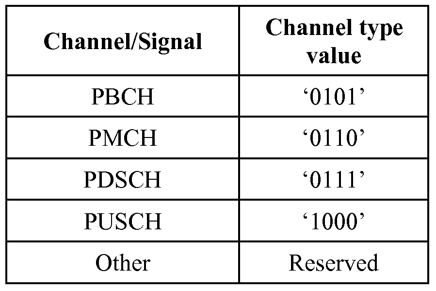
- Table 3 gives the values of the four selector bits m 44 through m 47 for different channel/signal types, in accordance with one design.
- a periodicity of 10 ms may be assumed for the PRS with normal cyclic prefix and extended cyclic prefix, PDCCH, PDSCH and PUSCH.
- a periodicity of 40 ms may be assumed for the PBCH.
- a periodicity of 10, 20 or 40 ms may be assumed for the PCFICH, PHICH and PMCH.
- the CeIl ID parameter indicates a cell identifier (ID) for a cell transmitting a downlink reference signal.
- the SSC ID parameter indicates a specific secondary synchronization code (SSC) sequence among a set of available SSC sequences.
- the Antenna ID parameter indicates a specific antenna at a Node B.
- the Subframe ID parameter indicates a specific sub frame out of 10 sub frames in a radio frame.
- the Symbol ID parameter indicates a specific OFDMA symbol out of either 12 or 14 OFDMA symbols in a subframe.
- the Frequency_+/- parameter indicates whether a scrambling sequence is for positive or negative frequencies, as described below.
- Table 5 gives channel-specific fields for the PDCCH and PDSCH, in accordance with one design.
- the UE MAC ID parameter indicates a Medium Access Control (MAC) ID assigned to a UE.
- the Stream ID parameter indicates a data stream being sent on the PDSCH.
- the Code Block ID parameter indicates a specific code block being sent on the PDSCH.
- the design in Table 5 support scrambling as a function of the CeIl ID and the UE MAC ID for the PDSCH.
- Table 6 gives channel-specific fields for the PBCH and PCFICH, in accordance with one design.
- the Frame ID parameter indicates a specific radio frame.
- Table 7 gives channel-specific fields for the PHICH and PMCH, in accordance with one design. Table 7 - Channel-Specific Fields for PHICH and PMCH
- Table 8 gives channel-specific fields for the PUSCH in accordance with one design.
- a scrambling sequence for a channel or a signal may be generated based on a sequence selector value, which may comprise a set of parameter values for parameters/attributes of the channel or signal.
- the time periodicity of the scrambling sequence may be flexibly controlled by including the symbol ID, slot ID, subframe ID, frame ID, etc., in the set of parameters for the sequence selector.
- the scrambling sequence may be associated or disassociated with resource elements or blocks by including or excluding the resource element/block index in the set of parameters for the sequence selector.
- the scrambling sequence generator described herein may simplify generation of scrambling sequences for all channels and signals of interest.
- the scrambling sequence generator can generate scrambling sequences for current channels and signals as well as new channels and signals that may be added in the future. New channels, signals and/or parameters may be supported by using some of the reserved values to convey the new channels, signals and/or parameters.
- a single scrambling sequence generator may be used to generate scrambling sequences for all channels and signals.
- the scrambling sequence generator may be clocked as many times as needed for the longest scrambling sequence. For shorter scrambling sequences, only the initial part for the desired length may be generated.
- multiple instances of the scrambling sequence generator may be implemented, and each scrambling sequence generator may support one or more channels and/or signals. This design may be more suitable for certain hardware architectures.
- two scrambling sequences may be used to generate a downlink reference signal that may be sent on a variable system bandwidth.
- the system bandwidth may be 1.25, 2.5, 5, 10 or 20 MHz in LTE. It may be desirable to have a nested structure for the scrambling sequences for the downlink reference signal.
- the scrambling sequences for system bandwidth of 10 MHz should match the center part of the scrambling sequences for system bandwidth of 20 MHz.
- two scrambling sequences may be generated for the downlink reference signal and may be distinguished by the Frequency_+/- bit in the sequence selector.
- the scrambling sequences may be used as PRS sequences to generate the downlink reference signal.
- the first scrambling sequence may be used to scramble 'positive frequencies', and the second scrambling sequence may be used to scramble 'negative frequencies'.
- FIG. 4 shows a design of generating two scrambling sequences for the downlink reference signal.
- the first scrambling sequence includes N scrambling bits Mo through M N - I , where N is the maximum number of scrambling bits needed for the largest system bandwidth of 20 MHz.
- the second scrambling sequence includes N scrambling bits Vo through V N - I -
- the first scrambling sequence may be generated with the parameters shown in Table 4 and with the Frequency _+/- parameter set to ' 1 '.
- the second scrambling sequence may be generated with the same parameters but with the Frequency _+/- parameter set to '0'.
- the first scrambling sequence may be used to scramble positive frequencies starting from the smallest positive frequency.
- the center or DC subcarrier is typically not used.
- the first scrambling sequence may be mapped to subcarriers used for the downlink reference signal in the order of increasing frequency, as shown in FIG. 4.
- the second scrambling sequence may be used to scramble 'negative frequencies' starting from the highest negative frequency, i.e., the subcarrier closest to the DC subcarrier.
- the second scrambling sequence may be mapped to the subcarriers used for the downlink reference signal in the opposite direction.
- the entire first scrambling sequence may be used, and all N scrambling bits Mo through M N - I may be mapped to N positive subcarriers used for the downlink reference signal.
- the entire second scrambling sequence may also be used, and all N scrambling bits vo through V N - I may be mapped to N negative subcarriers used for the downlink reference signal.
- the initial portion of the first scrambling sequence may be used, and M scrambling bits U 0 through M M - I may be mapped to the M positive subcarriers used for the downlink reference signal.
- the initial portion of the second scrambling sequence may also be used, and M scrambling bits vo through V M - I may be mapped to the M negative subcarriers used for the downlink reference signal.
- M may be dependent on the system bandwidth and may be less than N.
- the scrambling sequence generation design shown in FIG. 4 ensures that the scrambling sequences in the center of the system band are the same irrespective of the system bandwidth. Furthermore, this design does not require the entire first and second scrambling sequences to be generated in each OFDMA symbol carrying the downlink reference signal. By mapping the start of the first and second scrambling sequences to the center of the system bandwidth and by traversing outwardly in both positive and negative frequency directions, as shown in FIG. 4, only scrambling bits that are actually used are generated. This design may simplify scrambling sequence generation and may avoid redundant operations. This design may also efficiently support different system bandwidths, different number of subcarriers used for the downlink reference signal, and different scrambling sequence lengths.
- the design in FIG. 4 may also allow for simultaneously generation of the first and second scrambling sequences for the positive and negative frequency parts of the downlink reference signal. If the scrambling sequences are very long, then the scrambling sequences may be partitioned into segments, and different segments of the scrambling sequences may be processed in parallel with multiple instances of the scrambling sequence generator. A memory may store the initial LFSR states for the scrambling sequence generator for each segment. [0054] In an alternative design, a single scrambling sequence of length 2N may be used to generate the downlink reference signal. The start of this scrambling sequence may be mapped to the leftmost (or most negative) frequency, and the scrambling sequence may traverse to the rightmost (or most positive) frequency.
- FIG. 5 shows a design of a process 500 for performing scrambling at a transmitter or descrambling at a receiver in a communication system.
- Process 500 may be performed by a Node B, a UE, or some other entity.
- An LFSR may be initialized to an initial state to generate a base scrambling sequence (block 512).
- a first scrambling sequence may be generated based on modulo- 2 addition of a selected combination of LFSR outputs, with the first scrambling sequence being a first cyclic shift of the base scrambling sequence (block 514).
- Scrambling or descrambling for a first channel may be performed with the first scrambling sequence, with the first channel being one of a set of channels and possibly signals supported by the base scrambling sequence (block 516).
- a second scrambling sequence may also be generated based on modulo-2 addition of a second selected combination of LFSR outputs, with the second scrambling sequence being a second cyclic shift of the base scrambling sequence.
- the first and second scrambling sequences may be generated in parallel based on different combinations of LFSR outputs. Scrambling or descrambling for a second channel or a reference signal may be performed with the second scrambling sequence.
- the LFSR may implement a single generator polynomial that is applicable for all supported channels and signals.
- the LFSR may be reset for each application of scrambling or descrambling for the first channel.
- the LFSR may be initialized to the same initial state for all supported channels and signals.
- FIG. 6 shows a design of a process 600 for generating the first scrambling sequence.
- Process 600 is one design of block 514 in FIG. 5.
- a channel type value for the first channel may be determined (block 612).
- At least one parameter value for at least one parameter of the first channel may also be determined (block 614).
- a sequence selector value for the first channel may be determined based on the channel type value and the at least one parameter value (block 616).
- the combination of LFSR outputs to perform modulo-2 addition may be determined based on the sequence selector value (block 618).
- the first scrambling sequence may be obtained by (i) selecting or deselecting each output bit of the LFSR based on the sequence selector value and (ii) summing the selected output bits of the LFSR with modulo-2 addition to obtain the first scrambling sequence.
- the sequence selector value may comprise a first set of bits that may be assigned different values for different channels and signals supported by the base scrambling sequence.
- the sequence selector value may also comprise a second set of bits for channel-specific or signal-specific parameters.
- the supported channels and signals may include a broadcast channel, a multicast channel, a downlink shared channel, a downlink control channel, an uplink shared channel, an uplink control channel, a reference signal, some other channel or signal, or any combination thereof.
- the channel-specific or signal-specific parameters may include a cell ID, an antenna ID, a frame ID, a subframe ID, a symbol ID, a UE ID, a stream ID, a code block ID, some other parameter, or any combination thereof.
- FIG. 7 shows a design of an apparatus 700 for performing scrambling or descrambling in a communication system.
- Apparatus 700 includes a module 712 to initialize a LFSR to an initial state to generate a base scrambling sequence, a module 714 to generate a first scrambling sequence based on modulo-2 addition of a selected combination of LFSR outputs, with the first scrambling sequence being a first cyclic shift of the base scrambling sequence, and a module 716 to perform scrambling or descrambling for a first channel with the first scrambling sequence, the first channel being one of a set of channels supported by the base scrambling sequence.
- FIG. 8 shows a design of a process 800 for processing a reference signal.
- Process 800 may be performed by a Node B, a UE, or some other entity.
- a first scrambling sequence may be generated based on a first cyclic shift of a base scrambling sequence (block 812).
- a second scrambling sequence may be generated based on a second cyclic shift of the base scrambling sequence (block 814).
- the first scrambling sequence may have its start mapped to the center of the system bandwidth and may traverse outwardly in positive frequency direction, e.g., as shown in FIG. 4 (block 816).
- the second scrambling sequence may have its start mapped to the center of the system bandwidth and may traverse outwardly in negative frequency direction, e.g., as also shown in FIG. 4 (block 818).
- Scrambling or descrambling for positive frequencies for a reference signal may be performed with the first scrambling sequence (block 820).
- Scrambling or descrambling for negative frequencies for the reference signal may be performed with the second scrambling sequence (block 82
- a first sequence selector value comprising a first value for a frequency polarity parameter (e.g., the Frequency_+/- parameter) may be determined.
- a second sequence selector value comprising a second value for the frequency polarity parameter may also be determined.
- the base scrambling sequence may be cyclically shifted based on the first sequence selector value to obtain the first scrambling sequence.
- the base scrambling sequence may also be cyclically shifted based on the second sequence selector value to obtain the second scrambling sequence.
- At least one scrambling sequence generator may be reset to a starting point.
- the first M scrambling bits of the first scrambling sequence may be generated with the scrambling sequence generator(s), where M is determined based on the system bandwidth.
- the first M scrambling bits of the second scrambling sequence may also be generated with the scrambling sequence generator(s).
- FIG. 9 shows a design of an apparatus 900 for processing a reference signal.
- Apparatus 900 includes a module 912 to generate a first scrambling sequence based on a first cyclic shift of a base scrambling sequence, a module 914 to generate a second scrambling sequence based on a second cyclic shift of the base scrambling sequence, a module 916 to map the start of the first scrambling sequence to the center of the system bandwidth and traverse outwardly in positive frequency direction, a module 918 to map the start of the second scrambling sequence to the center of the system bandwidth and traverse outwardly in negative frequency direction, a module 920 to perform scrambling or descrambling for positive frequencies for a reference signal with the first scrambling sequence, and a module 922 to perform scrambling or descrambling for negative frequencies for the reference signal with the second scrambling sequence.
- FIG. 10 shows a block diagram of a design of a Node B 110 and a UE 120, which may be one of the Node Bs and one of the UEs in FIG. 1.
- Node B 110 is equipped with T antennas 1034a through 1034t
- UE 120 is equipped with R antennas 1052a through 1052r, where in general T ⁇ 1 and R ⁇ 1 .
- a transmit processor 1020 may receive traffic data for one or more UEs from a data source 1012, process the traffic data for each UE based on one or more modulation and coding schemes selected for that UE, and provide symbols for shared/data channels. Transmit processor 1020 may receive and process broadcast and multicast data and provide symbols for broadcast and multicast channels. Transmit processor 1020 may also receive and process control information from a controller/processor 1040 and provide symbols for control channels. Transmit processor 1020 may also generate symbols for reference signals, synchronization signals, etc. Transmit processor 1020 may perform scrambling for different channels and signals, as described above.
- a transmit (TX) multiple-input multiple-output (MIMO) processor 1030 may multiplex the symbols for different channels and signals.
- TX MIMO processor 1030 may perform spatial processing (e.g., precoding) on the multiplexed symbols, if applicable, and provide T output symbol streams to T modulators (MODs) 1032a through 1032t.
- Each modulator 1032 may process a respective output symbol stream (e.g., for OFDM) to obtain an output sample stream.
- Each modulator 1032 may further process (e.g., convert to analog, amplify, filter, and upconvert) the output sample stream to obtain a downlink signal.
- T downlink signals from modulators 1032a through 1032t may be transmitted via T antennas 1034a through 1034t, respectively.
- antennas 1052a through 1052r may receive the downlink signals from Node B 110 and provide received signals to demodulators (DEMODs) 1054a through 1054r, respectively.
- Each demodulator 1054 may condition (e.g., filter, amplify, downconvert, and digitize) a respective received signal to obtain input samples and may further process the input samples (e.g., for OFDM) to obtain received symbols.
- a MIMO detector 1056 may obtain received symbols from all R demodulators 1054a through 1054r, perform MIMO detection on the received symbols if applicable, and provide detected symbols.
- a receive processor 1058 may process (e.g., demodulate, deinterleave, and decode) the detected symbols, provide decoded data for UE 120 to a data sink 1060, and provide decoded control information to a controller/processor 1080.
- traffic data from a data source 1062 and control information from controller/processor 1080 may be processed by a transmit processor 1064, further processed by a TX MIMO processor 1066 if applicable, conditioned by modulators 1054a through 1054r, and transmitted to Node B 110.
- the uplink signals from UE 120 may be received by antennas 1034, conditioned by demodulators 1032, processed by a MIMO detector 1036 if applicable, and further processed by a receive processor 1038 to obtain the traffic data and control information transmitted by UE 120.
- Controllers/processors 1040 and 1080 may direct the operation at Node B 110 and UE 120, respectively.
- Memories 1042 and 1082 may store data and program codes for Node B 110 and UE 120, respectively.
- a scheduler 1044 may schedule UEs for downlink and/or uplink transmission and may provide assignments of resources for the scheduled UEs.
- Process 500 in FIG. 5, process 600 in FIG. 6, process 800 in FIG. 8 and/or other processes for the techniques described herein may be performed by one or more processors at Node B I lO and also by one or more processors at UE 120.
- transmit processors 1020 and 1064 may perform process 500 and/or 600 for scrambling
- receive processors 1038 and 1058 may perform process 500 and/or 600 for descrambling
- Transmit processor 1020 may also perform process 800 for scrambling of a downlink reference signal
- receive processor 1058 may perform process 800 for descrambling of the downlink reference signal.
- DSP digital signal processor
- ASIC application specific integrated circuit
- FPGA field programmable gate array
- a general- purpose processor may be a microprocessor, but in the alternative, the processor may be any conventional processor, controller, microcontroller, or state machine.
- a processor may also be implemented as a combination of computing devices, e.g., a combination of a DSP and a microprocessor, a plurality of microprocessors, one or more microprocessors in conjunction with a DSP core, or any other such configuration.
- the steps of a method or algorithm described in connection with the disclosure herein may be embodied directly in hardware, in a software module executed by a processor, or in a combination of the two.
- a software module may reside in RAM memory, flash memory, ROM memory, EPROM memory, EEPROM memory, registers, hard disk, a removable disk, a CD-ROM, or any other form of storage medium known in the art.
- An exemplary storage medium is coupled to the processor such that the processor can read information from, and write information to, the storage medium.
- the storage medium may be integral to the processor.
- the processor and the storage medium may reside in an ASIC.
- the ASIC may reside in a user terminal.
- the processor and the storage medium may reside as discrete components in a user terminal.
- the functions described may be implemented in hardware, software, firmware, or any combination thereof. If implemented in software, the functions may be stored on or transmitted over as one or more instructions or code on a computer-readable medium.
- Computer-readable media includes both computer storage media and communication media including any medium that facilitates transfer of a computer program from one place to another.
- a storage media may be any available media that can be accessed by a general purpose or special purpose computer.
- such computer-readable media can comprise RAM, ROM, EEPROM, CD-ROM or other optical disk storage, magnetic disk storage or other magnetic storage devices, or any other medium that can be used to carry or store desired program code means in the form of instructions or data structures and that can be accessed by a general-purpose or special-purpose computer, or a general-purpose or special-purpose processor. Also, any connection is properly termed a computer-readable medium.
- Disk and disc includes compact disc (CD), laser disc, optical disc, digital versatile disc (DVD), floppy disk and blu-ray disc where disks usually reproduce data magnetically, while discs reproduce data optically with lasers. Combinations of the above should also be included within the scope of computer- readable media.
Landscapes
- Engineering & Computer Science (AREA)
- Signal Processing (AREA)
- Physics & Mathematics (AREA)
- Computer Networks & Wireless Communication (AREA)
- Theoretical Computer Science (AREA)
- General Physics & Mathematics (AREA)
- Spectroscopy & Molecular Physics (AREA)
- Power Engineering (AREA)
- Computational Mathematics (AREA)
- Mathematical Optimization (AREA)
- Pure & Applied Mathematics (AREA)
- General Engineering & Computer Science (AREA)
- Mathematical Analysis (AREA)
- Mobile Radio Communication Systems (AREA)
Abstract
Description


Claims
Priority Applications (6)
| Application Number | Priority Date | Filing Date | Title |
|---|---|---|---|
| BRPI0818523 BRPI0818523B1 (en) | 2007-10-04 | 2008-10-03 | scramble sequence generation in a communication system |
| CA2699452A CA2699452C (en) | 2007-10-04 | 2008-10-03 | Scrambling sequence generation in a communication system |
| KR1020107009910A KR101122607B1 (en) | 2007-10-04 | 2008-10-03 | Scrambling sequence generation in a communication system |
| EP08836289.2A EP2201733B1 (en) | 2007-10-04 | 2008-10-03 | Scrambling sequence generation in a communication system |
| JP2010528174A JP5301551B2 (en) | 2007-10-04 | 2008-10-03 | Scrambling sequence generation in communication systems |
| CN2008801101750A CN101816156B (en) | 2007-10-04 | 2008-10-03 | Scrambling sequence generation in a communication system |
Applications Claiming Priority (4)
| Application Number | Priority Date | Filing Date | Title |
|---|---|---|---|
| US97763807P | 2007-10-04 | 2007-10-04 | |
| US60/977,638 | 2007-10-04 | ||
| US12/244,678 US8848913B2 (en) | 2007-10-04 | 2008-10-02 | Scrambling sequence generation in a communication system |
| US12/244,678 | 2008-10-02 |
Publications (1)
| Publication Number | Publication Date |
|---|---|
| WO2009046330A1 true WO2009046330A1 (en) | 2009-04-09 |
Family
ID=40029180
Family Applications (1)
| Application Number | Title | Priority Date | Filing Date |
|---|---|---|---|
| PCT/US2008/078794 WO2009046330A1 (en) | 2007-10-04 | 2008-10-03 | Scrambling sequence generation in a communication system |
Country Status (10)
| Country | Link |
|---|---|
| US (2) | US8848913B2 (en) |
| EP (1) | EP2201733B1 (en) |
| JP (2) | JP5301551B2 (en) |
| KR (1) | KR101122607B1 (en) |
| CN (2) | CN101816156B (en) |
| BR (1) | BRPI0818523B1 (en) |
| CA (2) | CA2815570C (en) |
| RU (1) | RU2442278C2 (en) |
| TW (2) | TWI407734B (en) |
| WO (1) | WO2009046330A1 (en) |
Cited By (7)
| Publication number | Priority date | Publication date | Assignee | Title |
|---|---|---|---|---|
| CN101997568A (en) * | 2009-08-18 | 2011-03-30 | 华为技术有限公司 | Method and device for scrambling positioning reference signals |
| US9497020B1 (en) | 2015-05-26 | 2016-11-15 | International Business Machines Corporation | Initializing a descrambler |
| US9515813B1 (en) | 2015-05-26 | 2016-12-06 | International Business Machines Corporation | Initializing a descrambler |
| WO2020034570A1 (en) * | 2019-01-11 | 2020-02-20 | Zte Corporation | Remote interference mitigation resource configuration |
| US11006392B2 (en) * | 2018-05-31 | 2021-05-11 | Marvell Asia Pte, Ltd. | Methods and apparatus for descrambling received uplink transmissions |
| US11303481B2 (en) | 2017-01-11 | 2022-04-12 | Qualcomm Incorporated | Signal scrambling sequence techniques for wireless communications |
| US11758588B2 (en) | 2018-11-02 | 2023-09-12 | Zte Corporation | Interference management in wireless systems |
Families Citing this family (64)
| Publication number | Priority date | Publication date | Assignee | Title |
|---|---|---|---|---|
| US8848913B2 (en) | 2007-10-04 | 2014-09-30 | Qualcomm Incorporated | Scrambling sequence generation in a communication system |
| EP2241126B1 (en) * | 2008-01-03 | 2016-04-13 | Koninklijke Philips N.V. | Method of exchanging data between a base station and a mobile station. |
| US8787181B2 (en) * | 2008-01-14 | 2014-07-22 | Qualcomm Incorporated | Resource allocation randomization |
| US7729237B2 (en) | 2008-03-17 | 2010-06-01 | Lg Electronics Inc. | Method of transmitting reference signal and transmitter using the same |
| US8923249B2 (en) * | 2008-03-26 | 2014-12-30 | Qualcomm Incorporated | Method and apparatus for scrambling sequence generation in a communication system |
| US20090268910A1 (en) * | 2008-04-28 | 2009-10-29 | Samsung Electronics Co., Ltd. | Apparatus and method for initialization of a scrambling sequence for a downlink reference signal in a wireless network |
| US20100016072A1 (en) * | 2008-07-18 | 2010-01-21 | Tong Lai Yu | Group users authentication and authorization using time reversal transformation |
| JP5345688B2 (en) * | 2008-08-12 | 2013-11-20 | テレフオンアクチーボラゲット エル エム エリクソン(パブル) | Method and apparatus in communication system |
| US8464141B2 (en) * | 2008-08-13 | 2013-06-11 | Infineon Technologies Ag | Programmable error correction capability for BCH codes |
| US8170592B2 (en) * | 2008-09-12 | 2012-05-01 | Broadcom Corporation | Method and system for frame timing acquisition in evolved universal terrestrial radio access (EUTRA) |
| US20100172235A1 (en) * | 2009-01-06 | 2010-07-08 | Samsung Electronics Co., Ltd. | System and method for initialization of a scrambling sequence for a downlink reference signal |
| US9491615B2 (en) * | 2009-06-10 | 2016-11-08 | Telefonaktiebolaget Lm Ericsson (Publ) | Detection of collisions of radio coverage cell identifiers |
| CN102804868B (en) * | 2009-06-16 | 2016-01-20 | 夏普株式会社 | Mobile station apparatus, base station apparatus, wireless communications method and integrated circuit |
| CN101997570B (en) * | 2009-08-12 | 2014-04-30 | 中兴通讯股份有限公司 | Method and device for generating scrambler |
| US8923905B2 (en) | 2009-09-30 | 2014-12-30 | Qualcomm Incorporated | Scrambling sequence initialization for coordinated multi-point transmissions |
| US8948097B2 (en) * | 2009-09-30 | 2015-02-03 | Qualcomm Incorporated | UE-RS sequence initialization for wireless communication systems |
| US9432164B2 (en) | 2009-10-15 | 2016-08-30 | Qualcomm Incorporated | Method and apparatus for reference signal sequence mapping in wireless communication |
| US8400995B2 (en) | 2010-09-22 | 2013-03-19 | Freescale Semiconductor, Inc. | System and method for descrambling data |
| CN102437986B (en) * | 2010-09-29 | 2016-06-22 | 中兴通讯股份有限公司 | Reference signal mapping method and device |
| US8873384B2 (en) * | 2010-11-01 | 2014-10-28 | Cisco Technology, Inc. | Bandwidth indication in RTS/CTS frames |
| CN102833056B (en) * | 2011-06-17 | 2015-01-28 | 华为技术有限公司 | Method, base station and user equipment for performing channel treatment |
| KR101818441B1 (en) * | 2011-06-30 | 2018-01-16 | 삼성전자주식회사 | Device and method for processing data |
| US8793295B2 (en) * | 2011-07-18 | 2014-07-29 | Lsi Corporation | Method for fast calculation of the beginning of pseudo random sequences for long term evolution |
| CN103178883B (en) | 2011-12-26 | 2016-09-14 | 华为技术有限公司 | The processing method of physical downlink control channel data, transmitting terminal and user terminal |
| US9167561B2 (en) * | 2012-03-12 | 2015-10-20 | Zte (Usa) Inc. | Sequence initialization for demodulation reference signal |
| US9847860B2 (en) * | 2012-03-23 | 2017-12-19 | Nokia Solutions And Networks Oy | Communication mechanism using demodulation reference signal based communication mode |
| US8923207B2 (en) * | 2012-05-17 | 2014-12-30 | Industrial Technology Research Institute | Method for initializing sequence of reference signal and base station using the same |
| US8838119B2 (en) | 2012-06-26 | 2014-09-16 | Futurewei Technologies, Inc. | Method and system for dynamic cell configuration |
| KR20150067751A (en) * | 2012-10-08 | 2015-06-18 | 엘지전자 주식회사 | Method for transceiving control information, and apparatus for same |
| US9444655B2 (en) * | 2014-03-25 | 2016-09-13 | Intel IP Corporation | Apparatus, method and system of scrambling a wireless transmission |
| US9350416B2 (en) * | 2014-05-07 | 2016-05-24 | Itron France | Frequency hopping sequence generation |
| CN105141558B (en) * | 2014-05-30 | 2019-02-01 | 华为技术有限公司 | Scrambling apparatus and scrambling configuration method |
| CN105472570A (en) * | 2014-09-03 | 2016-04-06 | 中兴通讯股份有限公司 | Base station/terminal and PDCCH scrambling/descrambling method and device thereof |
| CN104408356B (en) * | 2014-11-28 | 2017-11-24 | 北京大唐智能卡技术有限公司 | A kind of fingerprint verification method and system, fingerprint template encryption device |
| US11277390B2 (en) | 2015-01-26 | 2022-03-15 | Listat Ltd. | Decentralized cybersecure privacy network for cloud communication, computing and global e-commerce |
| US11627639B2 (en) | 2015-01-26 | 2023-04-11 | Ievgen Verzun | Methods and apparatus for HyperSecure last mile communication |
| US9998434B2 (en) | 2015-01-26 | 2018-06-12 | Listat Ltd. | Secure dynamic communication network and protocol |
| WO2016190799A1 (en) * | 2015-05-22 | 2016-12-01 | Telefonaktiebolaget Lm Ericsson (Publ) | Scrambling for downlink signaling in wireless communication network |
| EP3363140B1 (en) | 2015-10-12 | 2020-08-12 | Newracom, Inc. | Protection methods for wireless transmissions |
| US10405288B2 (en) * | 2016-02-25 | 2019-09-03 | Lg Electronics Inc. | Supporting various bandwidth |
| US10028203B2 (en) * | 2016-10-14 | 2018-07-17 | Qualcomm Incorporated | System information block transmission |
| CN108255464B (en) * | 2016-12-28 | 2021-09-28 | 北京忆恒创源科技股份有限公司 | Data scrambling method, descrambling method and device thereof |
| EP3566348A1 (en) * | 2017-01-06 | 2019-11-13 | IDAC Holdings, Inc. | Error check-based synchronization and broadcast channel |
| US10531494B2 (en) * | 2017-01-17 | 2020-01-07 | Huawei Technologies Co., Ltd. | Reference signal scrambling for random access |
| WO2018222224A1 (en) * | 2017-05-29 | 2018-12-06 | Intel IP Corporation | Apparatus, system and method of encoding a wireless transmission |
| WO2018236718A1 (en) | 2017-06-19 | 2018-12-27 | Intel IP Corporation | Apparatus, system and method of encoding a wireless transmission |
| KR101976055B1 (en) | 2017-07-28 | 2019-05-08 | 엘지전자 주식회사 | The method and apparatus for transmitting and receiving broadcasting channel |
| CN111201732B (en) * | 2017-08-10 | 2023-10-03 | 艾普拉控股有限公司 | Method for generating physical broadcast channel signal, related apparatus and storage medium |
| US11121808B2 (en) * | 2017-09-08 | 2021-09-14 | Apple Inc. | Method and apparatus for channel coding in the fifth generation new radio system |
| US10911271B2 (en) * | 2017-09-11 | 2021-02-02 | Qualcomm Incorporated | PBCH scrambling design |
| US11647495B2 (en) * | 2017-10-06 | 2023-05-09 | Qualcomm Incorporated | Sequence generation and assignment |
| CN108513699B (en) * | 2018-04-27 | 2019-11-15 | 北京小米移动软件有限公司 | The determination method and data de-scrambling method of the scrambled initialization sequence of data |
| JP7193614B2 (en) * | 2018-07-31 | 2022-12-20 | テレフオンアクチーボラゲット エルエム エリクソン(パブル) | Structures, methods, transmitters, transceivers and access points suitable for low complexity implementation |
| CN109257088B (en) * | 2018-08-14 | 2021-07-02 | 深圳市科楠科技开发有限公司 | Data descrambling system and method |
| CN110868279B (en) * | 2018-08-27 | 2021-09-14 | 华为技术有限公司 | Signal sending and receiving method and device |
| KR102569156B1 (en) * | 2018-09-28 | 2023-08-21 | 지티이 코포레이션 | Systems and methods for bit level signal processing |
| JP7201804B2 (en) * | 2018-11-01 | 2023-01-10 | オッポ広東移動通信有限公司 | Data scrambling method and device, communication equipment |
| US10991409B2 (en) * | 2019-07-19 | 2021-04-27 | SK Hynix Inc. | Encoder for memory system and method thereof |
| CN110943955B (en) * | 2019-10-31 | 2022-06-28 | 北京时代民芯科技有限公司 | Method for generating parallel scrambler |
| CN111049769A (en) * | 2019-11-27 | 2020-04-21 | Tcl华星光电技术有限公司 | Signal transmission method and device |
| CN114598416A (en) * | 2020-12-04 | 2022-06-07 | 华为技术有限公司 | Scrambling method, descrambling method, scrambling circuit and descrambling circuit |
| US20230093484A1 (en) * | 2021-09-23 | 2023-03-23 | Apple Inc. | Systems and methods for de-correlating coded signals in dual port transmissions |
| CN114244474B (en) * | 2021-12-20 | 2024-02-13 | 深圳忆联信息系统有限公司 | Scrambling code generation method, device, equipment and storage medium |
| CN114884711B (en) * | 2022-04-26 | 2023-12-26 | 邦彦技术股份有限公司 | Data processing method, device, system, equipment, control device and storage medium |
Family Cites Families (67)
| Publication number | Priority date | Publication date | Assignee | Title |
|---|---|---|---|---|
| US3995115A (en) * | 1967-08-25 | 1976-11-30 | Bell Telephone Laboratories, Incorporated | Speech privacy system |
| SU966864A1 (en) | 1980-12-02 | 1982-10-15 | Минский радиотехнический институт | Device for shaping biased copies of pseudorandom sequencies |
| US4811394A (en) * | 1982-07-28 | 1989-03-07 | Communications Satellite Corporation | Variable starting state scrambling circuit |
| SU1387177A1 (en) | 1985-02-20 | 1988-04-07 | Минский радиотехнический институт | Pseudorandom number generator |
| GB2182229B (en) * | 1985-10-25 | 1989-10-04 | Racal Res Ltd | Speech scramblers |
| US5111416A (en) | 1989-02-20 | 1992-05-05 | Clarion Co., Ltd. | Pseudo random noise code generator for selectively generating a code or its mirror image from common data |
| US5568483A (en) | 1990-06-25 | 1996-10-22 | Qualcomm Incorporated | Method and apparatus for the formatting of data for transmission |
| US5491718A (en) | 1994-01-05 | 1996-02-13 | Nokia Mobile Phones Ltd. | CDMA radiotelephone having optimized slotted mode and long code operation |
| US6831905B1 (en) | 1995-06-30 | 2004-12-14 | Interdigital Technology Corporation | Spread spectrum system assigning information signals to message-code signals |
| NZ500194A (en) | 1997-03-21 | 2000-12-22 | Canal Plus Sa | Broadcasting randomized subscriber entitlement management messages for digital television |
| US7184426B2 (en) | 2002-12-12 | 2007-02-27 | Qualcomm, Incorporated | Method and apparatus for burst pilot for a time division multiplex system |
| JPH11340799A (en) | 1998-05-28 | 1999-12-10 | Oki Electric Ind Co Ltd | Circuit and method for generating m sequence and circuit for generating pn sequence |
| US6798736B1 (en) * | 1998-09-22 | 2004-09-28 | Qualcomm Incorporated | Method and apparatus for transmitting and receiving variable rate data |
| KR100480286B1 (en) | 1999-04-02 | 2005-04-06 | 삼성전자주식회사 | Address generating apparatus and method for turbo interleaving |
| KR20000066904A (en) | 1999-04-21 | 2000-11-15 | 윤종용 | Apparatus and method for generating spreading code in cdma communications system |
| CA2526112C (en) | 1999-07-07 | 2012-09-18 | Samsung Electronics Co., Ltd. | Apparatus and method for generating scrambling code in umts mobile communication system |
| JP2001024624A (en) | 1999-07-12 | 2001-01-26 | Oki Electric Ind Co Ltd | Device and method for generating and processing code group |
| KR100429545B1 (en) | 1999-08-17 | 2004-04-28 | 삼성전자주식회사 | Method for communicating scrambling code id in mobile communication system |
| CN1141806C (en) * | 2000-03-01 | 2004-03-10 | 深圳市中兴通讯股份有限公司 | Scrambler/descrambler for synchronizing parallel frames in synchronous optical digital transmission system |
| DE60009052T2 (en) | 2000-07-21 | 2004-10-21 | St Microelectronics Nv | RAKE receiver for a CDMA system, especially in a cellular mobile phone |
| US6922435B2 (en) | 2000-09-29 | 2005-07-26 | Qualcomm Inc | Method and apparatus for generating PN sequences at arbitrary phases |
| US6985516B1 (en) | 2000-11-27 | 2006-01-10 | Qualcomm Incorporated | Method and apparatus for processing a received signal in a communications system |
| US7386026B1 (en) | 2001-04-09 | 2008-06-10 | Robert Gold Communication Systems, Inc. | Method and system for synchronizing and selectively addressing multiple receivers in a wireless, spread spectrum communication system |
| ATE445986T1 (en) | 2001-05-14 | 2009-10-15 | Ericsson Ab | METHOD AND SYSTEM FOR RESERVING TIME SLOTS IN A TDMA SYSTEM |
| JP3694479B2 (en) * | 2001-12-07 | 2005-09-14 | 松下電器産業株式会社 | Multi-carrier transceiver apparatus, multi-carrier wireless communication method, and multi-carrier wireless communication program |
| GB2384660B (en) | 2002-01-25 | 2004-11-17 | Toshiba Res Europ Ltd | Reciever processing systems |
| US7003269B2 (en) | 2002-02-20 | 2006-02-21 | Qualcomm Incorporated | Method and apparatus for a dedicated physical channel in a wireless communication system |
| EP1343265B1 (en) * | 2002-03-07 | 2006-05-31 | STMicroelectronics S.r.l. | A process for generating codes for CDMA communications, system and computer program |
| US7236512B2 (en) | 2002-09-09 | 2007-06-26 | Qualcomm Incorporated | Code channel allocations in a wireless communications system |
| CN1689259A (en) | 2002-09-09 | 2005-10-26 | 高通股份有限公司 | Code channel allocations in a wireless communications system |
| US7415112B2 (en) | 2002-09-18 | 2008-08-19 | Zarbana Digital Fund Llc | Parallel scrambler/descrambler |
| RU2330379C2 (en) | 2002-09-27 | 2008-07-27 | Айбиквити Диджитал Корпорейшн | Method and device for signal bits interleaving in digital sound broadcasting system |
| KR100920726B1 (en) * | 2002-10-08 | 2009-10-07 | 삼성전자주식회사 | Single carrier transmission system and a method using the same |
| RU2359412C2 (en) | 2002-10-25 | 2009-06-20 | Квэлкомм Инкорпорейтед | Random access for wireless communication systems with multiple access |
| US8169944B2 (en) | 2002-10-25 | 2012-05-01 | Qualcomm Incorporated | Random access for wireless multiple-access communication systems |
| US8208364B2 (en) | 2002-10-25 | 2012-06-26 | Qualcomm Incorporated | MIMO system with multiple spatial multiplexing modes |
| US7308063B2 (en) | 2002-12-20 | 2007-12-11 | Nokia Corporation | Apparatus, and associated method, for effectuating post-FFT correction of fine frequency offset |
| US20040223472A1 (en) * | 2003-03-06 | 2004-11-11 | Sankaran Sundar G. | Data randomization in a wireless communication system |
| JP2004274403A (en) | 2003-03-07 | 2004-09-30 | Sony Ericsson Mobilecommunications Japan Inc | Data sending method, data receiving method, data transmitting method, data sending apparatus, data receiving apparatus, and data transmission system |
| US7286589B1 (en) * | 2003-08-29 | 2007-10-23 | National Semiconductor Corporation | Method and apparatus for generation of downlink scrambling code in wideband CDMA mobile devices |
| US8498650B2 (en) | 2003-12-05 | 2013-07-30 | Qualcomm Incorporated | Systems and methods for adaptively allocating resources between a dedicated reference signal and a traffic signal |
| US7672285B2 (en) * | 2004-06-28 | 2010-03-02 | Dtvg Licensing, Inc. | Method and apparatus for minimizing co-channel interference by scrambling |
| US8391410B2 (en) | 2004-07-29 | 2013-03-05 | Qualcomm Incorporated | Methods and apparatus for configuring a pilot symbol in a wireless communication system |
| KR100925911B1 (en) | 2004-07-29 | 2009-11-09 | 콸콤 인코포레이티드 | System and method for diversity interleaving |
| CN100571092C (en) | 2004-11-30 | 2009-12-16 | 中兴通讯股份有限公司 | Method for forming pseudo mask register in the scrambling code phase deviation |
| JP4571523B2 (en) | 2005-03-04 | 2010-10-27 | ルネサスエレクトロニクス株式会社 | Scramble circuit, encoding apparatus, encoding method, and recording apparatus |
| US8340216B2 (en) | 2005-03-18 | 2012-12-25 | Qualcomm Incorporated | Space-time scrambling for cellular systems |
| JP4463780B2 (en) | 2005-06-14 | 2010-05-19 | 株式会社エヌ・ティ・ティ・ドコモ | Transmitting apparatus and transmitting method |
| KR100682062B1 (en) | 2005-06-23 | 2007-02-15 | 삼성전자주식회사 | RFID System and method for resolving RFID tags collision |
| US20070008944A1 (en) | 2005-07-06 | 2007-01-11 | Qian Zhang | Method and system for spreading and scrambling downlike physical channels |
| JP2007028289A (en) | 2005-07-19 | 2007-02-01 | Sharp Corp | Mobile communication system and communication method |
| US20070037541A1 (en) | 2005-08-15 | 2007-02-15 | Research In Motion Limited | Wireless Communications Device Including a Joint Space-Time Optimum Filter (JSTOF) Using Cholesky and Eigenvalue Decompositions |
| WO2007023810A1 (en) | 2005-08-23 | 2007-03-01 | Matsushita Electric Industrial Co., Ltd. | Scalable bandwidth system, radio base station apparatus, synchronous channel transmitting method and transmission method |
| EP1987607B1 (en) * | 2006-02-06 | 2013-11-20 | LG Electronics Inc. | Mbms dual receiver |
| US20090129448A1 (en) | 2006-02-15 | 2009-05-21 | Joshua Lawrence Koslov | Apparatus and Method For Generating Scrambling Codes |
| US8098745B2 (en) | 2006-03-27 | 2012-01-17 | Texas Instruments Incorporated | Random access structure for wireless networks |
| WO2007127902A2 (en) | 2006-04-27 | 2007-11-08 | Texas Instruments Incorporated | Methods and apparatus to allocate reference signals in wireless communication systems |
| JP4256410B2 (en) * | 2006-07-27 | 2009-04-22 | 株式会社東芝 | Wireless communication apparatus and transmission method |
| US7778151B2 (en) | 2006-10-03 | 2010-08-17 | Texas Instruments Incorporated | Efficient scheduling request channel for wireless networks |
| DK2100402T3 (en) | 2006-12-29 | 2012-03-05 | Nokia Corp | Apparatus, methods and computer software products that provide limited use of Zadoff-Chu sequences in pilot or pre-sample signals |
| WO2008123037A1 (en) | 2007-03-20 | 2008-10-16 | Ntt Docomo, Inc. | Base station device, user device, and method used in mobile communication system |
| CA2684364C (en) | 2007-04-30 | 2014-02-04 | Nokia Siemens Networks Oy | Coordinated cyclic shift and sequence hopping for zadoff-chu, modified zadoff-chu, and block-wise spreading sequences |
| US8077693B2 (en) | 2007-09-19 | 2011-12-13 | Samsung Electronics Co., Ltd. | Resource remapping and regrouping in a wireless communication system |
| US8848913B2 (en) | 2007-10-04 | 2014-09-30 | Qualcomm Incorporated | Scrambling sequence generation in a communication system |
| US8301912B2 (en) | 2007-12-31 | 2012-10-30 | Sandisk Technologies Inc. | System, method and memory device providing data scrambling compatible with on-chip copy operation |
| US8787181B2 (en) | 2008-01-14 | 2014-07-22 | Qualcomm Incorporated | Resource allocation randomization |
| US8923249B2 (en) | 2008-03-26 | 2014-12-30 | Qualcomm Incorporated | Method and apparatus for scrambling sequence generation in a communication system |
-
2008
- 2008-10-02 US US12/244,678 patent/US8848913B2/en active Active
- 2008-10-03 TW TW097138336A patent/TWI407734B/en active
- 2008-10-03 CA CA2815570A patent/CA2815570C/en active Active
- 2008-10-03 WO PCT/US2008/078794 patent/WO2009046330A1/en active Application Filing
- 2008-10-03 JP JP2010528174A patent/JP5301551B2/en active Active
- 2008-10-03 BR BRPI0818523 patent/BRPI0818523B1/en active IP Right Grant
- 2008-10-03 KR KR1020107009910A patent/KR101122607B1/en active IP Right Grant
- 2008-10-03 RU RU2010117383/08A patent/RU2442278C2/en active
- 2008-10-03 CN CN2008801101750A patent/CN101816156B/en active Active
- 2008-10-03 CA CA2699452A patent/CA2699452C/en active Active
- 2008-10-03 CN CN201310174888.6A patent/CN103354533B/en active Active
- 2008-10-03 EP EP08836289.2A patent/EP2201733B1/en active Active
- 2008-10-03 TW TW102115978A patent/TWI493935B/en active
-
2012
- 2012-08-29 JP JP2012188916A patent/JP5657618B2/en active Active
-
2014
- 2014-09-29 US US14/500,150 patent/US9622246B2/en active Active
Non-Patent Citations (3)
| Title |
|---|
| CHOI D-W: "PARALLEL SCRAMBLING TECHNIQUES FOR DIGITAL MULTIPLEXERS", AT & T TECHNICAL JOURNAL, AMERICAN TELEPHONE AND TELEGRAPH CO. NEW YORK, US, vol. 65, no. 5, 1 September 1986 (1986-09-01), pages 123 - 136, XP000616778, ISSN: 8756-2324 * |
| JIAN REN ET AL: "CDMA physical layer built-in security enhancement", VEHICULAR TECHNOLOGY CONFERENCE, 2003. VTC 2003-FALL. 2003 IEEE 58TH ORLANDO, FL, USA 6-9 OCT. 2003; [IEEE VEHICULAR TECHNOLGY CONFERENCE], PISCATAWAY, NJ, USA,IEEE, US, vol. 3, 6 October 2003 (2003-10-06), pages 2157 - 2161, XP010701813, ISBN: 978-0-7803-7954-1 * |
| WALTHER U ET AL: "Pn-generators embedded in high performance signal processors", ISCAS 2001. PROCEEDINGS OF THE 2001 IEEE INTERNATIONAL SYMPOSIUM ON CIRCUITS AND SYSTEMS. SYDNEY, AUSTRALIA, MAY 6 - 9, 2001; [IEEE INTERNATIONAL SYMPOSIUM ON CIRCUITS AND SYSTEMS], NEW YORK, NY : IEEE, US, vol. 4, 6 May 2001 (2001-05-06), pages 45 - 48, XP010541788, ISBN: 978-0-7803-6685-5 * |
Cited By (11)
| Publication number | Priority date | Publication date | Assignee | Title |
|---|---|---|---|---|
| CN101997568A (en) * | 2009-08-18 | 2011-03-30 | 华为技术有限公司 | Method and device for scrambling positioning reference signals |
| US9497020B1 (en) | 2015-05-26 | 2016-11-15 | International Business Machines Corporation | Initializing a descrambler |
| US9515813B1 (en) | 2015-05-26 | 2016-12-06 | International Business Machines Corporation | Initializing a descrambler |
| US9548857B2 (en) | 2015-05-26 | 2017-01-17 | International Business Machines Corporation | Initializing a descrambler |
| US9565014B2 (en) | 2015-05-26 | 2017-02-07 | International Business Machines Corporation | Initializing a descrambler |
| US11303481B2 (en) | 2017-01-11 | 2022-04-12 | Qualcomm Incorporated | Signal scrambling sequence techniques for wireless communications |
| US11006392B2 (en) * | 2018-05-31 | 2021-05-11 | Marvell Asia Pte, Ltd. | Methods and apparatus for descrambling received uplink transmissions |
| US20210243729A1 (en) * | 2018-05-31 | 2021-08-05 | Marvell Asia Pte, Ltd. | Methods and apparatus for descrambling received uplink transmissions |
| US11647485B2 (en) * | 2018-05-31 | 2023-05-09 | Marvell Asia Pte Ltd. | Methods and apparatus for descrambling received uplink transmissions |
| US11758588B2 (en) | 2018-11-02 | 2023-09-12 | Zte Corporation | Interference management in wireless systems |
| WO2020034570A1 (en) * | 2019-01-11 | 2020-02-20 | Zte Corporation | Remote interference mitigation resource configuration |
Also Published As
| Publication number | Publication date |
|---|---|
| CN103354533B (en) | 2017-04-12 |
| JP5301551B2 (en) | 2013-09-25 |
| CN101816156A (en) | 2010-08-25 |
| JP2013034207A (en) | 2013-02-14 |
| US8848913B2 (en) | 2014-09-30 |
| TW201351934A (en) | 2013-12-16 |
| JP5657618B2 (en) | 2015-01-21 |
| CA2815570A1 (en) | 2009-04-09 |
| CA2699452A1 (en) | 2009-04-09 |
| KR20100060033A (en) | 2010-06-04 |
| US9622246B2 (en) | 2017-04-11 |
| CA2699452C (en) | 2014-09-23 |
| US20090136034A1 (en) | 2009-05-28 |
| EP2201733A1 (en) | 2010-06-30 |
| CA2815570C (en) | 2015-09-08 |
| EP2201733B1 (en) | 2020-01-22 |
| TWI493935B (en) | 2015-07-21 |
| TW200929964A (en) | 2009-07-01 |
| BRPI0818523B1 (en) | 2019-12-03 |
| US20150016396A1 (en) | 2015-01-15 |
| JP2010541500A (en) | 2010-12-24 |
| KR101122607B1 (en) | 2012-03-16 |
| BRPI0818523A2 (en) | 2016-07-19 |
| RU2010117383A (en) | 2011-12-10 |
| CN101816156B (en) | 2013-11-06 |
| CN103354533A (en) | 2013-10-16 |
| TWI407734B (en) | 2013-09-01 |
| RU2442278C2 (en) | 2012-02-10 |
Similar Documents
| Publication | Publication Date | Title |
|---|---|---|
| US9622246B2 (en) | Scrambling sequence generation in a communication system | |
| RU2431930C2 (en) | Method and apparatus for multiplexing cdm pilot signal and fdm data | |
| KR101115146B1 (en) | Frequency diverse transmissions in a wireless communication system | |
| EP2158715B1 (en) | Pilot structures for ack and cqi in a wireless communication system | |
| KR101312443B1 (en) | Transmission of reference signal on non-contiguous clusters of resources | |
| KR101176321B1 (en) | Secondary synchronization codebook for e-utran | |
| EP2158685A1 (en) | Assignment of primary and secondary synchronization code sequences to cells in a wireless communication system | |
| WO2009023792A1 (en) | Reference signal generation in a wireless communication system |
Legal Events
| Date | Code | Title | Description |
|---|---|---|---|
| WWE | Wipo information: entry into national phase |
Ref document number: 200880110175.0 Country of ref document: CN |
|
| 121 | Ep: the epo has been informed by wipo that ep was designated in this application |
Ref document number: 08836289 Country of ref document: EP Kind code of ref document: A1 |
|
| WWE | Wipo information: entry into national phase |
Ref document number: 2699452 Country of ref document: CA |
|
| WWE | Wipo information: entry into national phase |
Ref document number: 1448/CHENP/2010 Country of ref document: IN |
|
| WWE | Wipo information: entry into national phase |
Ref document number: 2010528174 Country of ref document: JP |
|
| NENP | Non-entry into the national phase |
Ref country code: DE |
|
| WWE | Wipo information: entry into national phase |
Ref document number: 2008836289 Country of ref document: EP |
|
| ENP | Entry into the national phase |
Ref document number: 20107009910 Country of ref document: KR Kind code of ref document: A |
|
| WWE | Wipo information: entry into national phase |
Ref document number: 2010117383 Country of ref document: RU |
|
| REG | Reference to national code |
Ref country code: BR Ref legal event code: B01E Ref document number: PI0818523 Country of ref document: BR Free format text: REGULARIZE A PROCURACAO, UMA VEZ QUE A MESMA FOI APRESENTADA SEM DATA |
|
| ENP | Entry into the national phase |
Ref document number: PI0818523 Country of ref document: BR Kind code of ref document: A2 Effective date: 20100401 |