US9830983B1 - Memory system and writing method - Google Patents
Memory system and writing method Download PDFInfo
- Publication number
- US9830983B1 US9830983B1 US15/437,371 US201715437371A US9830983B1 US 9830983 B1 US9830983 B1 US 9830983B1 US 201715437371 A US201715437371 A US 201715437371A US 9830983 B1 US9830983 B1 US 9830983B1
- Authority
- US
- United States
- Prior art keywords
- data
- stage
- program
- threshold
- memory cells
- Prior art date
- Legal status (The legal status is an assumption and is not a legal conclusion. Google has not performed a legal analysis and makes no representation as to the accuracy of the status listed.)
- Active
Links
Images


Classifications
-
- G—PHYSICS
- G11—INFORMATION STORAGE
- G11C—STATIC STORES
- G11C11/00—Digital stores characterised by the use of particular electric or magnetic storage elements; Storage elements therefor
- G11C11/56—Digital stores characterised by the use of particular electric or magnetic storage elements; Storage elements therefor using storage elements with more than two stable states represented by steps, e.g. of voltage, current, phase, frequency
- G11C11/5621—Digital stores characterised by the use of particular electric or magnetic storage elements; Storage elements therefor using storage elements with more than two stable states represented by steps, e.g. of voltage, current, phase, frequency using charge storage in a floating gate
- G11C11/5628—Programming or writing circuits; Data input circuits
-
- G—PHYSICS
- G11—INFORMATION STORAGE
- G11C—STATIC STORES
- G11C16/00—Erasable programmable read-only memories
- G11C16/02—Erasable programmable read-only memories electrically programmable
- G11C16/04—Erasable programmable read-only memories electrically programmable using variable threshold transistors, e.g. FAMOS
- G11C16/0483—Erasable programmable read-only memories electrically programmable using variable threshold transistors, e.g. FAMOS comprising cells having several storage transistors connected in series
-
- G—PHYSICS
- G11—INFORMATION STORAGE
- G11C—STATIC STORES
- G11C16/00—Erasable programmable read-only memories
- G11C16/02—Erasable programmable read-only memories electrically programmable
- G11C16/06—Auxiliary circuits, e.g. for writing into memory
- G11C16/08—Address circuits; Decoders; Word-line control circuits
-
- G—PHYSICS
- G11—INFORMATION STORAGE
- G11C—STATIC STORES
- G11C16/00—Erasable programmable read-only memories
- G11C16/02—Erasable programmable read-only memories electrically programmable
- G11C16/06—Auxiliary circuits, e.g. for writing into memory
- G11C16/10—Programming or data input circuits
-
- G—PHYSICS
- G11—INFORMATION STORAGE
- G11C—STATIC STORES
- G11C16/00—Erasable programmable read-only memories
- G11C16/02—Erasable programmable read-only memories electrically programmable
- G11C16/06—Auxiliary circuits, e.g. for writing into memory
- G11C16/24—Bit-line control circuits
-
- G—PHYSICS
- G11—INFORMATION STORAGE
- G11C—STATIC STORES
- G11C16/00—Erasable programmable read-only memories
- G11C16/02—Erasable programmable read-only memories electrically programmable
- G11C16/06—Auxiliary circuits, e.g. for writing into memory
- G11C16/26—Sensing or reading circuits; Data output circuits
-
- G—PHYSICS
- G11—INFORMATION STORAGE
- G11C—STATIC STORES
- G11C16/00—Erasable programmable read-only memories
- G11C16/02—Erasable programmable read-only memories electrically programmable
- G11C16/06—Auxiliary circuits, e.g. for writing into memory
- G11C16/32—Timing circuits
-
- G—PHYSICS
- G11—INFORMATION STORAGE
- G11C—STATIC STORES
- G11C16/00—Erasable programmable read-only memories
- G11C16/02—Erasable programmable read-only memories electrically programmable
- G11C16/06—Auxiliary circuits, e.g. for writing into memory
- G11C16/34—Determination of programming status, e.g. threshold voltage, overprogramming or underprogramming, retention
- G11C16/3436—Arrangements for verifying correct programming or erasure
- G11C16/3454—Arrangements for verifying correct programming or for detecting overprogrammed cells
- G11C16/3459—Circuits or methods to verify correct programming of nonvolatile memory cells
-
- G—PHYSICS
- G11—INFORMATION STORAGE
- G11C—STATIC STORES
- G11C2211/00—Indexing scheme relating to digital stores characterized by the use of particular electric or magnetic storage elements; Storage elements therefor
- G11C2211/56—Indexing scheme relating to G11C11/56 and sub-groups for features not covered by these groups
- G11C2211/564—Miscellaneous aspects
- G11C2211/5648—Multilevel memory programming, reading or erasing operations wherein the order or sequence of the operations is relevant
Definitions
- Embodiments described herein relate generally to a memory system and a writing method.
- NAND memories capable of storing 3 bits/cell
- a method of simultaneously writing all bits similarly on adjacent cells after simultaneously writing all of the stored bits on first memory cells, and subsequently rewriting all of the bits on the first memory cells again is generally used.
- this method it is necessary to retain data on a controller side to execute the rewriting.
- 1-3-3 coding is known. This method is coding in which 7 among 8 regions with threshold voltages of 3 bits/cell are divided into 1, 3, and 3 with 3 bits.
- FIG. 1 is a block diagram illustrating an example of the configuration of a storage device according to a first embodiment.
- FIG. 2 is a block diagram illustrating an example of the configuration of a nonvolatile memory according to the first embodiment.
- FIG. 3 is a diagram illustrating an example of the configuration of a block of a memory cell array with a 3-dimensional structure.
- FIG. 4 is a sectional view illustrating a partial region of the memory cell array of a NAND memory with a 3-dimensional structure.
- FIG. 5 is a diagram illustrating examples of threshold voltage regions according to the first embodiment.
- FIG. 6 is a diagram illustrating data coding according to the first embodiment.
- FIG. 7 is a diagram illustrating threshold voltage distributions after program according to the first embodiment.
- FIG. 8A is a diagram illustrating a first example of a program procedure according to the first embodiment.
- FIG. 8B is a diagram illustrating a second example of a program procedure according to the first embodiment.
- FIG. 8C is a diagram illustrating a third example of a program procedure according to the first embodiment.
- FIG. 9A is a flowchart illustrating an example of a write procedure corresponding one entire block according to the first embodiment.
- FIG. 9B is a sub-flowchart illustrating a write procedure in a first stage according to the first embodiment.
- FIG. 9C is a sub-flowchart illustrating a write procedure in a second stage according to the first embodiment.
- FIG. 9D is a sub-flowchart illustrating a modification example of a write procedure in the second stage according to the first embodiment.
- FIG. 9E is a diagram illustrating a majority decision process of read results of a plurality of times.
- FIG. 10A is a diagram illustrating the amount of data of a buffer in LM-foggy-fine program in which 1-3-3 coding is adopted.
- FIG. 10B is a diagram illustrating the amount of data of a buffer in the program according to the first embodiment.
- FIGS. 11A and 11B illustrate examples of sequences of external program commands according to the first embodiment.
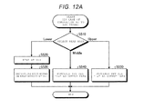
- FIG. 12A is a flowchart illustrating a process procedure of page reading in a word line in which program is completed up to the first stage in the storage device according to the first embodiment.
- FIG. 12B is a flowchart illustrating a process procedure of page reading in a word line in which program is completed up to the second stage in a storage device according to the first embodiment.
- FIGS. 13A and 13B illustrate examples of sequences of an external read command according to the first embodiment.
- FIG. 14A is a flowchart illustrating a write procedure corresponding one entire block according to a second embodiment.
- FIG. 14B is a sub-flowchart illustrating a write procedure of a first stage and a second stage according to the second embodiment.
- FIG. 15 is a diagram illustrating an example of a sequence of external program commands according to the second embodiment.
- FIG. 16 is a diagram illustrating data destruction caused due to power shutdown.
- FIG. 17 is a diagram illustrating program of a second stage according to a third embodiment.
- FIG. 18 is a flowchart illustrating a write procedure in the second stage according to the third embodiment.
- FIG. 19 is a diagram illustrating a modification example of the program of the second stage according to the third embodiment.
- FIGS. 20A, 20B, and 20C are diagrams illustrating another example of 1-3-3 data coding.
- FIG. 21 is a diagram illustrating threshold voltage distributions after program according to a fourth embodiment.
- FIG. 22A is a sub-flowchart illustrating a write procedure in a first stage according to the fourth embodiment.
- FIG. 22B is a sub-flowchart illustrating a write procedure in a second stage according to the fourth embodiment.
- FIG. 22C is a sub-flowchart illustrating a modification example of the write procedure in the second stage according to the fourth embodiment.
- FIGS. 23A and 23B illustrate examples of sequences of external program commands according to the fourth embodiment.
- FIG. 24A is a flowchart illustrating a process procedure of page reading in a word line in which program is completed up to the first stage in a storage device according to the fourth embodiment.
- FIG. 24B is a flowchart illustrating a process procedure of page reading in a word line in which program is completed up to the second stage in a storage device according to the fourth embodiment.
- FIGS. 25A and 25B illustrate examples of sequences of an external read command according to the fourth embodiment.
- FIG. 26 is a diagram illustrating the configuration of a flag cell.
- FIG. 27A is a diagram illustrating program to a flag cell according to a fifth embodiment.
- FIG. 27B is a diagram illustrating program to a dummy cell according to the fifth embodiment.
- FIG. 28 is a flowchart illustrating a write procedure in a second stage according to the fifth embodiment.
- FIG. 29 is a flowchart illustrating a process procedure of page reading according to the fifth embodiment.
- FIG. 30 is a diagram illustrating an example of sequence of an external read command according to the fifth embodiment.
- FIG. 31 is a diagram illustrating examples of threshold voltage regions according to a sixth embodiment.
- FIG. 32 is a diagram illustrating a first example indicating threshold voltage distributions after program according to the sixth embodiment.
- FIG. 33 is a diagram illustrating data coding corresponding to the threshold voltage distributions illustrated in FIG. 32 .
- FIG. 34 is a diagram illustrating a second example indicating threshold voltage distributions after program according to the sixth embodiment.
- FIG. 35 is a diagram illustrating data coding corresponding to the threshold voltage distributions illustrated in FIG. 34 .
- FIG. 36 is a diagram illustrating a third example indicating threshold voltage distributions after program according to the sixth embodiment.
- FIG. 37 is a diagram illustrating data coding corresponding to the threshold voltage distributions illustrated in FIG. 35 .
- Embodiments provide a memory system and a writing method capable of reducing an amount of write buffers in a memory controller while suppressing interference between cells.
- a nonvolatile memory device includes a memory cell array including first memory cells and second memory cells, a plurality of bit lines, each of which is connected to one of the first memory cells and one of the second memory cells, a first word line connected to gates of the first memory cells, a second word line connected to gates of the second memory cells, and a control unit configured to perform an operation to write first, second, and third pages of data in the first memory cells in first and second stages.
- the control unit applies voltages to the first word line and the bit lines based on the first page of data to maintain threshold voltages for a first group of the first memory cells and shift the threshold voltages for a second group of the first memory cells above a first threshold.
- control unit applies voltages to the first word line and the bit lines based on the second and third pages of data so as to shift the threshold voltages of the first memory cells in the first group to threshold voltages that are in one of first, second, and third threshold voltage ranges and the threshold voltages of the first memory cells in the second group to threshold voltages that are in one of fourth, fifth, sixth, and seventh threshold voltage ranges.
- FIG. 1 is a block diagram illustrating an example of the configuration of a storage device according to a first embodiment.
- a storage device according to the present embodiment includes a memory controller 1 and a nonvolatile memory 2 .
- the storage device can be connected to a host.
- the host is, for example, an electronic apparatus such as a personal computer or a portable terminal.
- the nonvolatile memory 2 is a memory that stores data in a nonvolatile manner and includes, for example, a NAND memory (NAND flash memory).
- NAND memory NAND flash memory
- the nonvolatile memory 2 is assumed to be a NAND memory that includes memory cells into which 3 bits per memory cell are stored, that is, a NAND memory storing 3 bits/cell (TLC: Triple Level Cell).
- TLC Triple Level Cell
- the nonvolatile memory 2 is also a 3-dimensional memory.
- the memory controller 1 controls write of data on the nonvolatile memory 2 in response to a write command from the host.
- the memory controller 1 controls read of data from the nonvolatile memory 2 in response to a read command from the host.
- the memory controller 1 includes a random access memory (RAM) 11 , a processor 12 , a host interface 13 , an error check and correction (ECC) circuit 14 , and a memory interface 15 .
- the RAM 11 , the processor 12 , the host interface 13 , the ECC circuit 14 , and the memory interface 15 are connected to each other by an internal bus 16 .
- the host interface 13 outputs commands, user data (write data), and the like received from the host to the internal bus 16 .
- the host interface 13 transmits the user data read from the nonvolatile memory 2 , a response from the processor 12 , and the like to the host.
- the memory interface 15 controls a process of writing user data or the like in the nonvolatile memory 2 and a process of reading user data or the like from the nonvolatile memory 2 based on instructions of the processor 12 .
- the processor 12 controls the memory controller 1 .
- the processor 12 is, for example, a central processing unit (CPU) or a micro processing unit (MPU).
- CPU central processing unit
- MPU micro processing unit
- the processor 12 executes control in response to the command.
- the processor 12 instructs the memory interface 15 to write user data and parity in the nonvolatile memory 2 in response to a command from a host.
- the processor 12 instructs the memory interface 15 to read user data and parity from the nonvolatile memory 2 in response to a command from the host.
- the processor 12 determines a storage region (memory region) in the nonvolatile memory 2 for the user data accumulated in the RAM 11 .
- the user data is stored in the RAM 11 via the internal bus 16 .
- the processor 12 determines a memory region for the user data in unit of pages which are units of writing (page data).
- page data units of writing
- user data stored in one page of the nonvolatile memory 2 is defined as unit data.
- the unit data is generally coded and is stored as a codeword in the nonvolatile memory 2 .
- the coding is optional.
- the memory controller 1 may store the unit data in the nonvolatile memory 2 without coding the unit data, but a configuration for executing the coding is illustrated as one configuration example in FIG. 1 .
- the page data is identical to the unit data.
- One codeword may be generated based on one piece of unit data or one codeword may be generated based on split data obtained by splitting the unit data.
- One codeword may be generated using a plurality of pieces of unit data.
- the processor 12 determines the memory region of the nonvolatile memory 2 of a write destination for each piece of unit data.
- a physical address is allocated to the memory region of the nonvolatile memory 2 .
- the processor 12 manages the memory region of the write destination of the unit data using the physical address.
- the processor 12 instructs the memory interface 15 to designate the determined memory region (physical address) and write the user data in the nonvolatile memory 2 .
- the processor 12 manages the mapping between a logical address (a logical address managed by the host) and a physical address of the user data. When the processor 12 receives a read command including the logical address from the host, the processor 12 determines the physical address corresponding to the logical address and instructs the memory interface 15 to output a command to read the user data from the physical address.
- memory cells commonly connected to one word line are defined as a memory cell group MG.
- the nonvolatile memory 2 is a NAND memory with TLC memory cells and one memory cell group MG corresponds to 3 pages.
- each of the 3 bits of the memory cells in a memory cell group corresponds to one of the 3 pages.
- the 3 pages are referred to as a lower page (first page), a middle page (second page), and an upper page (third page).
- the ECC circuit 14 codes the user data stored in the RAM 11 to generate a codeword.
- the ECC circuit 14 decodes the codeword read from the nonvolatile memory 2 .
- the RAM 11 temporarily stores the user data received from the host until the user data is stored in the nonvolatile memory 2 or temporarily stores data read from the nonvolatile memory 2 until the data is transmitted to the host.
- the RAM 11 is, for example, a general volatile memory such as a static random access memory (SRAM) and a dynamic random access memory (DRAM).
- FIG. 1 illustrates an example of the configuration in which the memory controller 1 includes the ECC circuit 14 and the memory interface 15 .
- the ECC circuit 14 may be contained in the memory interface 15 .
- the ECC circuit 14 may be contained in the nonvolatile memory 2 .
- the storage device When a write request is received from the host, the storage device (memory system) operates as follows.
- the processor 12 temporarily stores write data in the RAM 11 .
- the processor 12 reads data stored in the RAM 11 and inputs the data to the ECC circuit 14 .
- the ECC circuit 14 codes the input data and inputs the codeword to the memory interface 15 .
- the memory interface 15 writes the input codeword on the nonvolatile memory 2 .
- the storage device When a read request is received from the host, the storage device operates as follows.
- the memory interface 15 inputs the codeword read from the nonvolatile memory 2 to the ECC circuit 14 .
- the ECC circuit 14 decodes the input codeword and stores the decoded data in the RAM 11 .
- the processor 12 transmits the data stored in the RAM 11 to the host via the host interface 13 .
- a plurality of chips are connected in some cases, and the nonvolatile memory 2 and the memory interface 15 can also be connected via a through-silicon-via (TSV).
- TSV through-silicon-via
- FIG. 2 is a block diagram illustrating an example of the configuration of a nonvolatile memory according to the present embodiment.
- the nonvolatile memory 2 includes a NAND I/O interface 21 , a control unit 22 , a NAND memory cell array (memory cell unit) 23 , and a page buffer 24 .
- the nonvolatile memory 2 is formed from, for example, a semiconductor substrate (for example, a silicon substrate).
- the control unit 22 controls an operation of the nonvolatile memory 2 based on a command or the like input from the memory controller 1 via the NAND I/O interface 21 . Specifically, when a write request is input, the control unit 22 executes control such that data requested to be written is written to a designated address on the NAND memory cell array 23 . When a read request is input, the control unit 22 executes control such that data request to be read is read from the NAND memory cell array 23 and is output to the memory controller 1 via the NAND I/O interface 21 .
- the page buffer 24 temporarily stores data input from the memory controller 1 at the time of writing of the NAND memory cell array 23 or temporarily stores data read from the NAND memory cell array 23 .
- FIG. 3 is a diagram illustrating an example of the configuration of a block of a memory cell array with a 3-dimensional structure.
- FIG. 3 illustrates one block BLK among a plurality of blocks included in a memory cell array with a 3-dimensional structure.
- the other blocks of the memory cell array have the same configuration of that in FIG. 3 .
- the present embodiment can also be applied to a memory cell with a 2-dimensional structure.
- the block BLK includes, for example, 4 fingers FNG (FNG 0 to FNG 3 ).
- Each of the fingers FNG includes a plurality of NAND strings NS.
- Each of the NAND strings NS includes, for example, 8 memory cell transistors MT (MT 0 to MT 7 ) and select transistors ST 1 and ST 2 .
- the number of memory cell transistors MT is not limited to 8.
- the memory cell transistors MT are arranged between the select transistors ST 1 and ST 2 so that current paths are connected in series.
- the current path of the memory cell transistor MT 7 on one end side of the series connection is connected to one end of the current path of the select transistors ST 1 and the current path of the memory cell transistors MT 0 the other end side is connected to one end of the current path of the select transistor ST 2 .
- Gates of the select transistors ST 1 of the fingers FNG 0 to FNG 3 are commonly connected to select gate line SGD 0 to SGD 3 .
- the gates of the select transistors ST 2 are commonly connected to the same select gate line SGS across the plurality of fingers FNG.
- Control gates of the memory cell transistors MT 0 to MT 7 in the same block BLK are commonly connected to word lines WL 0 to WL 7 . That is, the word lines WL 0 to WL 7 and the select gate lines SGS are commonly connected across the plurality of fingers FNG 0 to FNG 3 in the same block BLK, and the select gate lines SGD are independent from each other among the fingers FNG 0 to FNG 3 even in the same block BLK.
- the NAND string NS is referred to as a string in some cases.
- Each memory cell is connected to the word line WLi and is also connected to a bit line.
- Each memory cell can be identified by addresses that identify the word line WLi and the select gate lines SGD 0 to SGD 3 and an address that identifies the bit line.
- data of memory cells (the memory cell transistors MT) in the same block BLK is erased collectively.
- reading and writing of data are executed in units of physical sectors MS.
- One physical sector MS is connected to one word line WLi and includes a plurality of memory cells belonging to one finger FNG.
- one word line WLi and one select gate line SGD are selected and the physical sector MS is selected according to a physical address.
- FIG. 4 is a sectional view illustrating a partial region of the memory cell array of a NAND memory with a 3-dimensional structure.
- a plurality of NAND strings NS are formed on a p-type well region (P-well). That is, a plurality of wiring layers 333 functioning as the select gate lines SGS, a plurality of wiring layers 332 functioning as word lines WLi, and a plurality of wiring layers 331 functioning as the select gate lines SGD are formed on the p-type well region.
- memory holes 334 penetrating through these wiring layers 333 , 332 , and 331 and reaching the p-type well region are formed.
- Block insulation films 335 , charge accumulation layers 336 , and gate insulation films 337 are sequentially formed on side surfaces of the memory holes 334 , and additional conductive films 338 (e.g., polysilicon films) are embedded in the memory holes 334 .
- the conductive film 338 functions as the current path of the NAND string NS and is a region in which channels are formed at the time of operation of the memory cell transistors MT and the select transistors ST 1 and ST 2 .
- each NAND string NS the select transistor ST 2 , the plurality of memory cell transistors MT, and the select transistor ST 1 are sequentially stacked on the p-type well region.
- a wiring layer functioning as a bit line BL is formed at the upper end of the conductive film 338 .
- an n+ type impurity diffusion layer and a p+ type impurity diffusion layer are formed on an upper surface of the p-type well region.
- a contact plug 340 is formed on the n+ type impurity diffusion layer and a wiring layer functioning as a source line SL is formed on the contact plug 340 .
- a contact plug 339 is formed on the p+ type impurity diffusion layer and a wiring layer functioning as well wiring CPWELL is formed on the contact plug 339 .
- the plurality of foregoing configurations illustrated in FIG. 4 are arrayed in a depth direction of the sheet surface in FIG. 4 and one finger FNG is formed by a set of the plurality of NAND strings aligned in the depth direction.
- FIG. 5 is a diagram illustrating examples of threshold voltage regions according to the first embodiment.
- FIG. 5 illustrates an example of a threshold distribution for a memory cell containing 3 bits/cell.
- information is stored by the amount of charge accumulated in a floating gate of the memory cell.
- Each memory cell has a threshold voltage in accordance with the amount of charge.
- a plurality of data values stored in the memory cell corresponds to a plurality of regions (threshold voltage regions) of the threshold voltages.
- 8 distributions denoted by Er, A, B, C, D, E, F, and G are threshold voltage distributions in the 8 threshold voltage regions. In this way, the 8 threshold voltage distributions are separated by 7 boundaries.
- the horizontal axis in FIG. 5 represents the threshold voltage and the vertical axis indicates a distribution of the number of memory cells (the number of cells).
- a region of which a threshold voltage is equal to or lower than Vr 1 is referred to as a region Er
- a region of which a threshold voltage is equal to or higher than Vr 1 and equal to or lower than Vr 2 is referred to as a region A
- a region of which a threshold voltage is equal to or higher than Vr 2 and equal to or lower than Vr 3 is referred to as a region B
- a region of which a threshold voltage is equal to or higher than Vr 3 and equal to or lower than Vr 4 is referred to as a region C.
- a region of which a threshold voltage is equal to or higher than Vr 4 and equal to or lower than Vr 5 is referred to as a region D
- a region of which a threshold voltage is equal to or higher than Vr 5 and equal to or lower than Vr 6 is referred to as a region E
- a region of which a threshold voltage is equal to or higher than Vr 6 and equal to or lower than Vr 7 is referred to as a region F
- a region of which a threshold voltage is equal to or higher than Vr 7 is referred to as a region G.
- the threshold voltage distributions corresponding to the regions Er, A, B, C, D, E, F, and G are referred to as distributions Er, A, B, C, D, E, F, and G (first to eighth distributions).
- Vr 1 to Vr 7 are threshold voltages at the boundaries of the regions.
- a plurality of data values correspond to the plurality of threshold voltage regions (that is, the threshold voltage distributions) of the memory cells.
- This correspondence is referred to as data coding.
- the data coding is determined in advance, and charges are injected into the memory cells in the threshold regions in accordance with the data values stored according to the data coding at the time of writing (program) of data. Then, at the time of reading, a read voltage is applied to the memory cell and data is determined depending on whether the threshold voltage of the memory cell is lower or higher than the read voltage.
- a data value in an “erased” state is defined as “1”.
- a “programmed” state is determined and data is defined as “0”.
- data is determined depending on whether the threshold voltage is lower or higher than a read level of a reading target boundary.
- an “erased” state is defined and the pieces of data of all bits are determined as “1”.
- a “programmed” state is determined and data is defined as “1” or “0” according to the coding.
- FIG. 6 is a diagram illustrating data coding according to the first embodiment.
- 8 threshold voltage distributions (threshold voltage regions) illustrated in FIG. 5 correspond to 8 data values of 3 bits.
- a relation between the threshold voltages and data values of bits corresponding to the upper, middle, and lower pages is as follows:
- the threshold voltage of the memory cell is within the Er region.
- data of only 1 bit is changed between 2 arbitrary adjacent states in such a manner that data of “111” is stored in the Er (erased) state and data of “101” is stored in the A state.
- the coding illustrated in FIG. 6 is gray coding in which data is changed by only 1 bit between 2 arbitrary adjacent regions.
- threshold voltages serving as boundaries for determining bit values of pages are as follows:
- the number of threshold voltages serving as the boundaries for determining bit values are 1, 3, and 3 for the lower page, the middle page, and the upper page, respectively.
- such coding is referred to as 1-3-3 coding using the numbers of boundaries of the lower page, the middle page, and the upper page.
- the matter to be noticed herein is that the maximum number of boundaries changed between pieces of adjacent data for each page is 3. The reason why the maximum of number of boundaries 3 is that when 8 states are expressed with 3 bits, the maximum number of boundaries is minimum and a deviation of a bit error is small.
- the control unit 22 of the nonvolatile memory 2 controls program to the NAND memory cell array 23 and read from the NAND memory cell array 23 based on the coding illustrated in FIG. 6 .
- the size of the memory cell is larger than that of a 2-dimensional NAND memory of a generation in which microfabrication is recently achieved and interference between cells is small.
- a method of simultaneously programming all bits is generally used.
- 1-2-4 coding or 2-3-2 coding is used as data coding.
- the 1-2-4 coding when 7 boundaries among 8 threshold voltage distributions are divided into 3 pages, the boundaries are divided in such a manner that 1 is divided to the lower page, 2 are divided to the middle page, and 4 are divided to the upper page.
- the 2-3-2 coding when 7 boundaries among 8 threshold voltage distributions are divided to 3 pages, the boundaries are divided in such a manner that 2 is divided to the upper page, 3 are divided to the middle page, and 2 are divided to the lower page.
- writing is executed with 3 program stages in such a manner that writing on an adjacent cell is executed after writing on a first stage (LM state), a return to the previous cell is executed, writing on further adjacent cell is executed again after writing on a second stage (foggy state), a return to the previous memory cell is executed again, and writing on a third stage (fine stage) is executed.
- each program stage is a program execution unit and program of 1 word line WLi is completed by executing 3 program stages.
- input data may be only lower page data.
- program of the foggy stage which is a second stage program is executed using 8 threshold voltage distributions.
- the threshold voltage distributions have larger widths than the threshold voltage distributions in final data coding. That is, in the foggy stage, foggy (rough) writing is executed.
- 3 pages are all required as input data. Since the threshold voltage distributions after the program of the foggy stage are an intermediate state in which adjacent distributions overlap each other, reading data may not be executed.
- the threshold voltage distribution after the program of the foggy stage are moved to threshold voltage distributions in the final data coding.
- fine writing is executed.
- 3 pages are all required as input data. Since the threshold voltage distributions after the program of the fine stage are in the final state in which adjacent distributions are separated, data can be read after the program of the fine stage.
- an amount of write buffer (a write buffer amount) for retaining data in order to input the data to a NAND memory may increase.
- the write buffer is a buffer to which some of regions of the RAM 11 included in the storage device is allocated.
- the write buffer amount is large despite application of the LM-foggy-fine program or the foggy-fine program in which the 1-3-3 coding is adopted, and thus the cost of the memory controller 1 increases.
- the 1-3-3 coding is adopted for the nonvolatile memory 2 having the 3-dimensional structure and writing in a page unit (page by page) is further executed in two stages.
- the write buffer amount of the memory controller 1 is reduced while suppressing interference between cells or a deviation in a bit error ratio between pages.
- interference between adjacent memory cells will be described. Charges accumulated in a floating gate of one certain memory cell disturb an electric field of an adjacent memory cell and consequently causes noise varying a threshold voltage of reading of the adjacent memory cell. Read precision deteriorates because verifying is executed with program under a certain electric field condition and the adjacent memory cell is programmed with different charges after completion of the program. The interference between adjacent memory cells becomes worse as a memory cell interval is reduced by a manufacturing technology for microfabrication of a memory device. Then, the interference between adjacent memory cells increases due to an adjacent memory cell of a different bit line on the same word line WLi and an adjacent memory cell of a different word line WLi on the same bit line.
- the interference between adjacent memory cells can be alleviated by reducing a difference between electric field conditions of the memory cells between the time of program and verifying and the time of reading after the adjacent memory cells are programmed.
- reducing the interference between adjacent memory cells between adjacent memory cells of different bit lines on the same word line WLi there is a method of splitting the program into a plurality of stages and executing the program of multi-stages at which a large change in charges between the stages is avoided.
- 3 bits on one word line WLi are programmed with 2 program stages, that is, a first stage and a second stage.
- Each program stage is a program execution unit and the storage device according to the present embodiment completes program of the word line WLi by executing the 2 program stages.
- any page of 3 bits can be allocated to each of the 2 program stages. Specifically, data of the lower page is allocated to the program of the first stage, and data of the middle and upper pages is allocated to the program of the second stage.
- FIG. 7 is a diagram illustrating threshold voltage distributions after program according to the first embodiment.
- FIG. 7 illustrates the threshold voltage distributions after the program of each stage on the memory cell.
- (T 1 ) in FIG. 7 illustrates a threshold voltage distribution in an erased state which is an initial state before the program.
- (T 2 ) in FIG. 7 illustrates a threshold voltage distribution after the program of the first stage.
- (T 3 ) in FIG. 7 illustrates a threshold voltage distribution after the program of the second stage.
- all the memory cells of the NAND memory cell array 23 are in a distribution Er state which is an unwritten state (the “erased” state).
- the control unit 22 of the nonvolatile memory 2 causes the distribution to remain in the distribution Er for each memory cell or injects charges and moves the distribution state to a distribution higher than the distribution Er according to a bit value written (stored) on the lower page in the program of the first stage, as illustrated in (T 2 ) in FIG. 7 .
- the control unit 22 does not inject charges.
- the control unit 22 injects charges and executes program so that the threshold voltage is moved to a higher voltage.
- the memory cells are programmed to 2-value levels by lower page data.
- a function in the program (first program) of the first stage is a function for only the lower page data. Page data necessary for this execution may be only the lower page.
- second program subsequent program
- data after the program of the first stage is binary, the lower page data can be read. Accordingly, in consideration of the fact that a level of the threshold voltage at the time of the program of the first stage is allocated to transition to D or higher through the program of the second stage, the level of the threshold voltage is controlled to be entered between Vr 1 and Vr 4 .
- program is executed by applying a program voltage pulse once or a plurality of times. After each program voltage pulse, reading is executed to confirm whether the memory cells are moved over a threshold voltage boundary level. By repeating the application and the reading, it is possible to move the threshold voltage of the memory cell within a range of a predetermined threshold voltage distribution.
- the control unit 22 may continuously execute the program of the first stage and the program of the second stage on one word line WLi.
- the control unit 22 may also execute the program across a plurality of word lines WLi in a non-continuous procedure in order to reduce the influence of the interference between adjacent memory cells.
- FIG. 8A is a diagram illustrating a first example of a program procedure according to the first embodiment.
- FIG. 8B is a diagram illustrating a second example of the program procedure according to the first embodiment.
- FIG. 8C is a diagram illustrating a third example of the program procedure according to the first embodiment.
- FIGS. 8A to 8C illustrate a sequence (a program method of two stages) in which an influence of interference between adjacent memory cells is reduced.
- FIG. 8A illustrates an example of the program procedure in the case of the NAND memory in which there is one string in a block.
- FIGS. 8B and 8C illustrate examples of the program procedure in the case of the NAND memory in which there are four strings in a block.
- control unit 22 proceeds to each program stage across the word lines WLi in a predetermined non-continuous procedure. That is, two different program stages are not continuously executed in the same word lines WLi.
- a change amount of the threshold voltage increases when the program of the first stage and the program of the second stage are executed in an adjacent word line WLi after completion of the program in the word lines WLi up to the second stage. Then, when the change amount of the threshold voltage of the adjacent word line WLi is large, the interference between the adjacent memory cells between the word lines WLi increases. Accordingly, in order to decrease the interference between the adjacent memory cells between the word lines WLi, it is effective to decrease the change amount of the threshold voltage values of the adjacent word lines WLi after the completion of the program in the word lines WLi up to the second stage. In such a sequence, the program stage of the adjacent word lines WLi after the completion of the program in the word lines WLi up to the second stage is only the second stage.
- the control unit 22 executes program in the order of the following (1) to (9) based on an instruction from the processor 12 .
- an operation of the program of the control unit 22 is based on an instruction from the processor 12 .
- the description that the operation is based on an instruction from the processor 12 will not be made.
- control unit 22 executes program ST 1 1 of the first stage of the word line WL 0 .
- control unit 22 executes program ST 1 2 of the first stage of the word line WL 1 .
- control unit 22 executes program ST 1 3 of the second stage of the word line WL 0 .
- control unit 22 executes program ST 1 4 of the first stage of the word line WL 2 .
- control unit 22 executes program ST 1 5 of the second stage of the word line WL 1 .
- control unit 22 executes program ST 1 6 of the first stage of the word line WL 3 .
- control unit 22 executes program ST 1 7 of the second stage of the word line WL 2 .
- control unit 22 executes program ST 1 8 of the first stage of the word line WL 4 .
- control unit 22 executes program ST 1 9 of the second stage of the word line WL 3 .
- control unit 22 progresses the process in the order indicated by arrows oriented right obliquely upward in the table illustrated in FIG. 8A .
- control unit 22 executes program in the order of the following (11) to (24).
- control unit 22 executes program ST 2 1 of the first stage of stringSt 0 _word line WL 0 .
- control unit 22 executes program ST 2 2 of the first stage of stringSt 1 _word line WL 0 .
- control unit 22 executes program ST 2 3 of the first stage of stringSt 2 _word line WL 0 .
- control unit 22 executes program ST 2 4 of the first stage of stringSt 3 _word line WL 0 .
- control unit 22 executes program ST 2 5 of the first stage of stringSt 0 _word line WL 1 .
- control unit 22 executes program ST 2 6 of the second stage of stringSt 0 _word line WL 0 .
- control unit 22 executes program ST 2 7 of the first stage of stringSt 1 _word line WL 1 .
- control unit 22 executes program ST 2 8 of the second stage of stringSt 1 _word line WL 0 .
- control unit 22 executes program ST 2 9 of the first stage of stringSt 2 _word line WL 1 .
- control unit 22 executes program ST 2 10 of the second stage of stringSt 2 _word line WL 0 .
- control unit 22 executes program ST 2 11 of the first stage of stringSt 3 _word line WL 1 .
- control unit 22 executes program ST 2 12 of the second stage of stringSt 3 _word line WL 0 .
- control unit 22 executes program ST 2 13 of the first stage of stringSt 0 _word line WL 2 .
- control unit 22 executes program ST 2 14 of the second stage of stringSt 0 _word line WL 1 .
- control unit 22 progresses the process in the order indicated by arrows oriented right obliquely upward in the table illustrated in FIG. 8B .
- FIG. 8B there are 4 strings in the block, as described above. However, there may be 3 or less strings or 5 or more strings in the block.
- control unit 22 executes program in the order of the following (31) to (50).
- control unit 22 executes program ST 3 1 of the first stage of stringSt 0 _word line WL 0 .
- control unit 22 executes program ST 3 2 of the first stage of stringSt 1 _word line WL 0 .
- control unit 22 executes program ST 3 3 of the first stage of stringSt 2 _word line WL 0 .
- control unit 22 executes program ST 3 4 of the first stage of stringSt 3 _word line WL 0 .
- control unit 22 executes program ST 3 5 of the first stage of stringSt 0 _word line WL 1 .
- control unit 22 executes program ST 3 6 of the first stage of stringSt 1 _word line WL 1 .
- control unit 22 executes program ST 3 7 of the first stage of stringSt 2 _word line WL 1 .
- control unit 22 executes program ST 3 8 of the first stage of stringSt 3 _word line WL 1 .
- control unit 22 executes program ST 3 9 of the second stage of stringSt 0 _word line WL 0 .
- control unit 22 executes program ST 3 10 of the second stage of stringSt 1 _word line WL 0 .
- control unit 22 executes program ST 3 11 of the second stage of stringSt 2 _word line WL 0 .
- control unit 22 executes program ST 3 12 of the second stage of stringSt 3 _word line WL 0 .
- control unit 22 executes program ST 3 13 of the first stage of stringSt 0 _word line WL 2 .
- control unit 22 executes program ST 3 14 of the first stage of stringSt 1 _word line WL 2 .
- control unit 22 executes program ST 3 15 of the first stage of stringSt 2 _word line WL 2 .
- control unit 22 executes program ST 3 16 of the first stage of stringSt 3 _word line WL 2 .
- control unit 22 executes program ST 3 17 of the second stage of stringSt 0 _word line WL 1 .
- control unit 22 executes program ST 3 18 of the second stage of stringSt 1 _word line WL 1 .
- control unit 22 executes program ST 3 19 of the second stage of stringSt 2 _word line WL 1 .
- control unit 22 executes program ST 3 20 of the second stage of stringSt 3 _word line WL 1 .
- FIG. 8C there are 4 strings in the block, as described above. However, there may be 3 or less strings or 5 or more strings in the block.
- the order of the program of the program stages of the word lines WLi in one string is the same as the order when there is one string.
- program of combination positions of the word lines WLi and the strings is progressed in such a general manner that the same word line number in different strings is first programmed and a subsequent word line number is progressed.
- FIGS. 9A to 9C illustrate the write procedure when write procedure follows the program procedure illustrated in FIG. 8B or 8C .
- the memory controller 1 progresses the program stages across the word lines WLi in the non-continuous procedure, and therefore executes program by setting a collection (here, a block) of certain word lines WLi as a collection of program sequences.
- FIG. 9A is a flowchart illustrating a first example of a write procedure corresponding one entire block according to the first embodiment.
- one block is assumed to have n+1 word lines WLi, word lines WL 0 to WLn (where n is a natural number).
- FIG. 9B is a sub-flowchart illustrating a write procedure in the first stage according to the first embodiment.
- FIG. 9C is a sub-flowchart illustrating a write procedure in the second stage according to the first embodiment. (1st) illustrated to the right of each step in FIG. 9A corresponds to the first stage illustrated in FIG. 9B and (2nd) corresponds to the second stage illustrated in FIG. 9C .
- the control unit 22 executes the program of the first stage of string St 0 _word line WL 0 (step S 10 ).
- the control unit 22 executes the program of the first stage of string St 1 _word line WL 0 (step S 20 ).
- the control unit 22 executes the same processes as steps S 10 and S 20 on each string.
- the control unit 22 executes the program of the first stage of string St 3 _word line WL 0 (step S 30 ).
- control unit 22 executes the program of the first stage of string St 0 _word line WL 1 (step S 40 ).
- the control unit 22 executes the program of the second stage of string St 0 _word line WL 0 (step S 50 ).
- the control unit 22 executes the program of the first stage of string St 1 _word line WL 1 (step S 60 ). Thereafter, the control unit 22 repeats the same processes as steps S 40 , S 50 , and S 60 on each word line WLi of each string.
- control unit 22 executes the program of the first stage of string St 0 _word line WLn (step S 70 ).
- the control unit 22 executes the program of the second stage of string St 0 _word line WLn ⁇ 1 (step S 80 ). Thereafter, the control unit 22 repeats the same processes as steps S 70 and S 80 on each word line WLi of each string.
- control unit 22 executes the program of the second stage of string St 3 _word line WLn ⁇ 1 (step S 90 ).
- control unit 22 executes the program of the second stage of string St 0 _word line WLn (step S 100 ).
- control unit 22 executes the program of the second stage of string St 1 _word line WLn (step S 110 ). Therefore, the control unit 22 executes the same processes as steps S 100 and S 110 on each string.
- the control unit 22 executes the program of the second stage of string St 3 _word line WLn (step S 120 ).
- a command to start inputting the lower page data is first input from the memory controller 1 to the nonvolatile memory 2 (step S 210 ). Then, the lower page data is input from the memory controller 1 to the nonvolatile memory 2 (step S 220 ). Further, a command to execute the program of the first stage is input from the memory controller 1 to the nonvolatile memory 2 (step S 230 ), and thus the chip becomes busy (step S 240 ).
- a program voltage pulse is applied once to a plurality of times (step S 250 ). Then, reading of the data is executed to confirm whether the memory cells are moved over the threshold voltage boundary level (step S 260 ).
- step S 270 it is confirmed whether the number of fail-bits of the data in the lower page is less than criteria (determination standard) (step S 270 ).
- the processes of steps S 250 to S 270 are repeated.
- the chip becomes ready (step S 280 ). In this way, by repeating the application, the reading, and the confirmation, it is possible to move the threshold voltage s of the memory cells within the range of the predetermined threshold voltage distribution.
- a command to start inputting the data of the middle page is first input from the memory controller 1 to the nonvolatile memory 2 in the program of the second stage (step S 310 ). Then, the data of the middle page is input from the memory controller 1 to the nonvolatile memory 2 (step S 320 ).
- a command to start inputting the data of the upper page is input from the memory controller 1 to the nonvolatile memory 2 (step S 330 ). Then, the data of the upper page is input from the memory controller 1 to the nonvolatile memory 2 (step S 340 ). Next, a command to execute the program of the second stage is input from the memory controller 1 to the nonvolatile memory 2 (step S 350 ), and thus the chip becomes busy (step S 360 ).
- control unit 22 executes reading of the lower page data as part of an internal data load (IDL) operation (step S 370 ). Then, the threshold voltages (hereinafter referred to as “Vth”) of program destinations of the middle and upper pages is determined based on the lower page data (step S 380 ). Thereafter, the data is written on the middle and upper pages using the determined Vth.
- Vth the threshold voltages
- control unit 22 can also execute reading a plurality of times, makes a majority decision of the read results with the page buffer 24 in the chip, and uses the result of the majority decision as subsequent write data.
- control unit 22 can also execute reading a plurality of times, makes a majority decision of the read result in the chip, and use the result of the majority decision as read data to the outside.
- FIG. 9E is a diagram illustrating a majority decision process of read results of a plurality of times.
- a correct bit is indicated with a circle ( ⁇ ) and an error bit is indicated by a cross (x).
- FIG. 9E illustrates results of the majority decision when the reading is executed three times.
- the program voltage pulse is applied once to a plurality of times (step S 390 ). Then, in order to confirm whether the memory cells are moved over the threshold voltage boundary level, reading of data of the middle and upper pages is executed (step S 400 ).
- step S 410 it is confirmed whether the number of fail-bits of the data in the middle and upper pages is less than the criteria.
- the processes of steps S 390 to S 410 are repeated.
- the chip becomes ready (step S 420 ).
- FIG. 9D is a sub-flowchart illustrating a modification example of the write procedure in the second stage according to the first embodiment.
- the process procedure illustrated in FIG. 9D is the same as the process procedure of steps S 310 to S 420 in FIG. 9C except that the process of step S 370 described in FIG. 9C is not executed.
- steps S 301 to S 309 are executed before step S 310 .
- a command to read the lower page is first input from the memory controller 1 to the nonvolatile memory 2 (step S 301 ), and thus the chip becomes busy (step S 302 ).
- control unit 22 executes the reading of the lower page data which is the IDL at the threshold voltage of Vr 4 . Then, the control unit 22 determines the value of the read data to “0” or “1” based on the read result at the threshold voltage of Vr 4 (step S 303 ). Thereafter, the chip becomes ready (step S 304 ).
- step S 305 When the lower page data read by the control unit 22 is output (step S 305 ), the lower page data is transmitted to the ECC circuit 14 (step S 306 ). Thus, the ECC circuit 14 executes ECC correction on the lower page data (step S 307 ).
- a command to start inputting the lower page data is input from the memory controller 1 to the nonvolatile memory 2 (step S 308 ).
- the ECC circuit 14 inputs the data of the lower page to the nonvolatile memory 2 (step S 309 ).
- step S 380 Vth of the program destinations of the middle and upper pages is determined based on the lower page data from the ECC circuit 14 .
- the control unit 22 first executes an operation of reading the lower page data as preprocessing, combining the lower page data with the data of the input middle and upper pages, and deciding Vth of the program destinations.
- the reason for reading the lower page data is that the 1-3-3 coding in which the number of boundaries of the lower page is 1 is adopted.
- the lower page data is read at the second stage, and thus it is not necessary to input the lower page data at the second stage. That is, since Vth of the program destination is determined based on the lower page data adopting the 1-3-3 coding, the interference between adjacent memory cells between the word lines WLi can be decreased, and thus one piece of page data is completely input by one-time data input.
- a memory amount necessary in the write buffer of the memory controller 1 is a plurality of word lines (a maximum of 7 pages). In the present embodiment, however, a memory amount necessary in the write buffer of the memory controller 1 is merely a maximum of 2 pages.
- FIG. 10A is a diagram illustrating the amount of data of a write buffer in the LM-foggy-fine program in which 1-3-3 coding is adopted.
- FIG. 10A and FIG. 10B to be described below illustrate time charts of input of write data of a block and execution of the program on the upper side and illustrate time charts of a period necessary to retain data in the write buffer on the lower side.
- FIG. 10A and FIG. 10B to be described below illustrate cases in which the number of strings in one block is 1. When the number of strings is plural, a memory amount corresponding to a multiple of the number of strings is necessary.
- the data corresponding to the 3 lower, middle, and upper pages is not continuously written to decrease the interference between the adjacent memory cells.
- the LM stage to the word line WL 0 is executed and before the foggy stage to the word line WL 0 is executed
- the LM stage to the word line WL 1 adjacent to the word line WL 0 is executed.
- the foggy stage to the word line WL 0 is executed and before the fine stage to the word line WL 0 is executed
- the foggy stage to the word line WL 1 adjacent to the word line WL 0 is executed.
- the LM stage to the word line WL 1 is executed and before the foggy stage to the word line WL 1 is executed, the LM stage to the word line WL 2 adjacent to the word line WL 1 is executed. Further, after the foggy stage to the word line WL 1 is executed and before the fine stage to the word line WL 1 is executed, the foggy stage to the word line WL 2 adjacent to the word line WL 1 is executed.
- FIG. 10B is a diagram illustrating the amount of data of a write buffer (a buffer data amount) in the program according to the first embodiment.
- the program of two stages is used with the 1-3-3 coding.
- input of the data corresponding to 1 page (the lower page) and the program (the first program) corresponding to 1 page are executed at the first stage.
- input of the data corresponding to 2 pages (the middle and upper pages) and the program (the second program) corresponding to 2 pages are executed at the second stage.
- the data may be stored in the write buffer.
- the data may be deleted from the write buffer. For example, when the data at the first stage is input, the data is stored in the write buffer. When the program at the first stage starts, the data stored in the write buffer may be deleted. Similarly, when the data at the second stage is input, the data is stored in the write buffer. When the program at the second stage starts, the data stored in the write buffer may be deleted.
- the data corresponding to the 3 lower, middle, and upper pages is not continuously written to decrease the interference between the adjacent memory cells.
- the first stage to the word line WL 1 adjacent to the word line WL 0 is executed.
- the first stage to the word line WL 2 adjacent to the word line WL 1 is executed.
- the program according to the present embodiment is the program of two stages, it takes a short time to execute the processes from the first stage to the second stage in each word line WLi.
- the program of the stage of the following (P11) is executed between the first stage and the second stage in the word line WL 1 :
- the data may be retained in the write buffer only between the start of the input of the data and the end of the input of the data.
- the data may be deleted from the write buffer. Therefore, in the case of the program according to the present embodiment, the data necessarily retained in the write buffer is data corresponding to a maximum of 2 pages.
- the data of all the pages is necessary in only the program of one-time stage.
- the data in the write buffer can be discarded. Therefore, the present embodiment, the number of pages necessarily retained simultaneously in the write buffer may be small.
- the page data programmed to the nonvolatile memory 2 is temporarily retained in the write buffer of the RAM 11 , and then is input to the nonvolatile memory 2 at the time of program.
- cost is reduced since the necessary capacity of the RAM 11 can be decreased.
- the data of all the pages has to be transmitted twice or three times. Therefore, it takes some time to transmit the data and extra power consumption is necessary at the time of transmission.
- the transmission time and the power consumption can be suppressed to about 1 ⁇ 2 to 1 ⁇ 3.
- FIGS. 11A and 11B are diagrams illustrating examples of sequences of external program commands according to the first embodiment.
- FIG. 11A illustrates a sequence of external program commands at the first stage according to the first embodiment.
- FIG. 11B illustrates a sequence of an external program command at the second stage according to the first embodiment.
- a program start command ( 80 h ) is input, the address of a program target block page (the address of the lower page) is subsequently input, and the program data of the lower page is subsequently input. Then, when a program execution command ( 10 h ) is finally input, the chip become busy and an operation of the program starts inside the memory chip. By inputting these program commands, the lower page is programmed.
- the program start command ( 80 h ) is input, the address of a program target block page (the address of the middle page) is subsequently input, and the program data of the middle page is subsequently input. Thereafter, a connection command ( 1 Ah) of the program command is input and the program data of the upper page is presently input in the same sequence. Then, when the program execution command ( 10 h ) is finally input, the chip become busy and an operation of the program starts inside the memory chip. By inputting these program commands, the reading of the lower page is executed and the middle and upper pages are further programmed. Either the program data of the middle page or the program data of the upper page may be input earlier.
- a page reading method is different according to before the program in regard to the word lines WLi including a reading target page is written on the second stage and after the program is completely written on the second stage.
- the control unit 22 Before the writing of the second stage, the written data is valid for only the lower page. Therefore, the control unit 22 reads the data from the memory cells only when the read data is the lower page. Then, when the read data is the other pages, the control unit 22 forcibly executes control such that all “1s” are output as the read data without executing an operation of reading the memory cells.
- the control unit 22 reads the memory cells of the read page which is any of the upper, middle, and lower pages. In this case, since a necessary read voltage is different according to which page is read, the control unit 22 executes only reading necessary according to the selected page.
- the control unit 22 determines data according to in which range the threshold voltage is located between 2 ranges separated by this boundary. For example, when the threshold voltage is lower than Vr 4 , the control unit 22 executes control such that “1” is output as data of the memory cell. Conversely, when the threshold voltage is higher than Vr 4 , the control unit 22 executes control such that “0” is output as data of the memory cell.
- control unit 22 determines data according to in which range the threshold voltage is located among 4 ranges separated by these boundaries.
- FIG. 12A is a flowchart illustrating a process procedure of page reading in the word line before writing of the second stage in the storage device according to the first embodiment.
- FIG. 12B is a flowchart illustrating a process procedure of page reading in the word line in which program is completed up to the second stage in the storage device according to the first embodiment.
- the control unit 22 selects a read page (step S 510 ).
- the control unit 22 executes reading at the threshold voltage of Vr 4 (step S 520 ). Then, the control unit 22 determines the value of the read data to “0” or “1” based on a read result at the threshold voltage of Vr 4 (step S 530 ).
- control unit 22 When the read page is the middle page (middle in step S 510 ), the control unit 22 forcibly executes control such that all “1s” are output as the output data of the memory cells (step S 540 ).
- control unit 22 When the read page is the upper page (upper in step S 510 ), the control unit 22 forcibly executes control such that all “1s” are output as the output data of the memory cells (step S 550 ).
- the control unit 22 selects a read page (step S 610 ).
- the control unit 22 executes reading at the threshold voltage of Vr 4 (step S 620 ). Then, the control unit 22 determines the value of the read data to “0” or “1” based on a read result at the threshold voltage of Vr 4 (step S 630 ).
- the control unit 22 executes the reading at the threshold voltages of Vr 1 , Vr 3 , and Vr 6 (steps S 640 , S 650 , and S 660 ). Then, the control unit 22 determines the value of the read data to “0” or “1” based on read results at the threshold voltages of Vr 1 , Vr 3 , and Vr 6 (step S 670 ).
- the control unit 22 executes the reading at the threshold voltages of Vr 2 , Vr 5 , and Vr 7 (steps S 680 , S 690 , and S 700 ). Then, the control unit 22 determines the value of the read data to “0” or “1” based on read results at the threshold voltages of Vr 2 , Vr 5 , and Vr 7 (step S 710 ).
- the memory controller 1 can manage and identify whether before or after the program in regard to the word lines WLi is completely written on the second stage.
- the memory controller 1 executes the control of the program. Therefore, when the memory controller 1 records a progress status, the memory controller 1 can easily refer to the address of the nonvolatile memory 2 and the state of the program at the address. In this case, when the memory controller 1 executes reading from the nonvolatile memory 2 , the memory controller 1 identifies a program state of the word line WLi including a target page address and issues a read command according to the identified state.
- FIGS. 13A and 13B are diagrams illustrating an example of a sequence of external read commands according to the first embodiment.
- FIG. 13A illustrates a sequence of external read commands in the word lines WLi in which the program is completed up to the first stage in the storage device according to the first embodiment.
- FIG. 13B illustrates a sequence of external read commands in the word lines WLi in which the program is completed up to the second stage in the storage device according to the first embodiment.
- a command ( 2 Dh) indicating a state before the writing of the second stage is first input as a command to execute a read operation. Thereafter, a read start command ( 00 h ) is input, and the address of a read target block page (the address of the lower page, the middle page, or the upper page) is subsequently input. Then, when a read execution command ( 30 h ) is finally input, the chip become busy and a reading operation inside the memory chip starts. By inputting these program commands, the data is read from the lower page, the middle page, or the upper page. Thereafter, the chip enters a ready state and the read data is output.
- a command ( 25 h ) indicating a completion state up to the second stage is first input as a command to execute a read operation. Thereafter, the read start command ( 00 h ) is input, and the address of a read target block page (the address of the lower page, the middle page, or the upper page) is subsequently input. Then, when the read execution command ( 30 h ) is finally input, the chip becomes busy and a reading operation inside the memory chip starts. By inputting these program commands, the data is read from the lower page, the middle page, or the upper page. Thereafter, the chip enters a ready state and the read data is output.
- the nonvolatile memory 2 (a NAND memory storing 3 bits/cell having a 3-dimensional structure or a 2-dimensional structure) is programmed
- the 1-3-3 data coding is adopted and the stages of the program is set to 2 stages.
- the nonvolatile memory 2 is programmed with 2 stages, the amount of data input at the time of programming the data can be reduced and the amount of a write buffer necessary for the memory controller 1 can be suppressed.
- a deviation of a bit error ratio between the pages of the nonvolatile memory 2 can be reduced and cost of ECC can be lowered. Since the data is transmitted once for each page, a transmission time and power consumption can be suppressed.
- each program stage is executed stepping the word line WLi, the amount of interference between adjacent cells with the adjacent word lines WLi can be reduced. Since the 1-3-3 data coding is used, an IDL margin before the second stage can be expanded, and thus reliability of the write sequence can be improved. Since the 1-3-3 data coding is used, the program of the first stage, that is, the program of the lower page, can be accelerated by setting the number of threshold voltage boundaries in the lower page as 1. The acceleration of the program of the first stage can be achieved by gradually stepping up the write voltage at the time of repeating the writing and verifying of the writing and setting a step voltage at the time of writing to be higher than the step voltage at the time of programming the second stage.
- FIGS. 14A, 14B, and 15 a second embodiment will be described with reference to FIGS. 14A, 14B, and 15 .
- the program of the second stage of the word line WLn ⁇ 1 and the program of the first stage of the word line WLn are executed collectively.
- the same data coding as the data coding described in FIG. 6 in the first embodiment is used in the description.
- the program of the first stage and the program of the second stage are both separated one by one, and each program command and each piece of program data are input at the time of each program.
- the program command and the program data are input collectively as soon as possible.
- program of the first stage of the word line WLn and program of the second stage of the word line WLn ⁇ 1 are inevitably continued except for end portions of the head and the final of the block. Accordingly, in the present embodiment, this portion is input with a mass of commands. That is, pieces of program data of the lower page of the word line WLn and the middle and upper page of the word line WLn ⁇ 1 are collectively input by inputting the commands once.
- the same amount of data as the amount of data input by 3 pages is input collectively in regard to the data of the lower, middle, and the upper pages (here, in this case the pages in the same word line WLi) with a one-time program command even when the LM-foggy-fine program is adopted.
- FIGS. 14A and 14B illustrate the write procedure when the write procedure follows the program procedure illustrated in FIG. 8B .
- the same processes as the processes described in FIGS. 9A to 9C among the processes illustrated in FIG. 14A or 14B will not be described.
- FIG. 14A is a flowchart illustrating an example of a write procedure corresponding one entire block according to a second embodiment.
- one block is assumed to include n+1 word lines WLi, the word lines WL 0 to WLn (where n is a natural number).
- FIG. 14B is a sub-flowchart illustrating a write procedure of the first stage and the second stage according to the second embodiment. (1st) illustrated to the right of each step in FIG. 14A corresponds to the first stage illustrated in FIG. 9B , (2nd) corresponds to the second stage illustrated in FIG. 9C , and (1, 2) corresponds to the first stage and the second stage illustrated in FIG. 14B .
- the control unit 22 executes the processes of steps S 810 to S 830 which are the same processes of steps S 10 to S 30 when writing starts.
- the program of the first stage of the word line WL 0 in the strings St 0 to St 3 is executed.
- control unit 22 executes the program of the first stage of stringSt 0 _word line WL 1 and the program of the second stage of stringSt 0 _word line WL 0 (step S 840 ).
- control unit 22 executes the program of the first stage of stringSt 1 _word line WL 1 and the program of the second stage of stringSt 1 _word line WL 0 (step S 850 ).
- control unit 22 executes the program of the first stage of stringSt 2 _word line WL 1 and the program of the second stage of stringSt 2 _word line WL 0 (step S 860 ). Thereafter, the control unit 22 repeats the same processes as those of steps S 840 , S 850 , and S 860 in regard to each word line WLi of each string.
- control unit 22 executes the program of the first stage of stringSt 0 _word line WLn and the program of the second stage of stringSt 0 _word line WLn ⁇ 1 (step S 870 ).
- control unit 22 executes the program of the first stage of stringSt 1 _word line WLn and the program of the second stage of stringSt 1 _word line WLn ⁇ 1 (step S 880 ). Thereafter, the control unit 22 repeats the same processes as those of steps S 870 and S 880 in regard to each word line WLi of each string.
- control unit 22 executes the program of the first stage of string St 3 _word line WLn and the program of the second stage of string St 3 _word line WLn ⁇ 1 (step S 890 ).
- control unit 22 executes the processes of steps S 900 to S 920 which are the same processes as those of steps S 100 to S 120 .
- the program of the second stage of the word lines WLn of the strings St 0 to St 3 is executed.
- the program of only the first stage is executed in the head of the block as in the first embodiment, and the program of only the second stage is executed in the final of the block as in the first embodiment.
- the program of only the first stage is executed in the procedure illustrated in FIG. 9B and the program of only the second stage is executed in the procedure illustrated in FIG. 9C .
- the program of the first stage is executed continuously after the program of the second stage is executed. Specifically, a command to start inputting the data of the middle page of the word line WLn ⁇ 1 is input from the memory controller 1 to the nonvolatile memory 2 (step S 1010 ). Then, the data of the middle page of the word line WLn ⁇ 1 is input from the memory controller 1 to the nonvolatile memory 2 (step S 1020 ).
- a command to start inputting the data of the upper page of the word line WLn ⁇ 1 is input from the memory controller 1 to the nonvolatile memory 2 (step S 1030 ). Then, the data of the upper page of the word line WLn ⁇ 1 is input from the memory controller 1 to the nonvolatile memory 2 (step S 1040 ).
- a command to start inputting the data of the lower page of the word line WLn is input from the memory controller 1 to the nonvolatile memory 2 (step S 1050 ). Then, the data of the lower page of the word line WLn is input from the memory controller 1 to the nonvolatile memory 2 (step S 1060 ).
- a command to execute the program of the first stage and the program of the second stage is input from the memory controller 1 to the nonvolatile memory 2 (step S 1070 ), and thus the chip becomes busy (step S 1080 ).
- step S 1090 the program voltage pulse is applied to the lower page of the word line WLn once to a plurality of times. Then, reading of the data of the lower page of the word line WLn is executed to confirm whether the memory cells are moved over the threshold voltage boundary level (step S 1100 ).
- step S 1110 it is confirmed whether the number of fail-bits of the data in the lower page is less than the criteria.
- the processes of steps S 1140 to S 1160 are repeated.
- the lower page data of the word line WLn ⁇ 1 is read (step S 1120 ).
- Vth threshold voltages of program destinations of the middle and upper pages is determined based on the lower page data of the word line WLn ⁇ 1 (step S 1130 ). Thereafter, data is written on the middle and upper pages of the word line WLn ⁇ 1 using the determined Vth.
- the program voltage pulse is applied to the middle and upper pages of the word line WLn ⁇ 1 once to a plurality of times (step S 1140 ). Then, reading of the data of the middle and upper pages of the word line WLn ⁇ 1 is executed to confirm whether the memory cells are moved over the threshold voltage boundary level (step S 1150 ).
- step S 1160 it is confirmed whether the number of fail-bits of the data in the middle and upper pages is less than the criteria.
- the processes of steps S 1140 to S 1160 are repeated.
- the chip becomes ready (step S 1170 ).
- any of the processes of steps S 1010 , S 1030 , and S 1050 may be executed earlier. Any of the processes of the steps S 1020 , S 1040 , and S 1060 may be executed earlier. However, the process of step S 1020 is executed later than the process of step S 1010 , the process of step S 1040 is executed later than the process of step S 1030 , and the process of step S 1060 is executed later than the process of step S 1050 .
- steps S 1120 to S 1160 illustrated in FIG. 14B correspond to the program of the second stage of the word line WLn ⁇ 1.
- steps S 1090 to S 1110 correspond to the program of the first stage of the word line WLn.
- the program of the first stage of the word line WLn is executed earlier than the program of the second stage of the word line WLn ⁇ 1, as described above with reference to FIG. 14B .
- the program of the first stage of the word line WLn is executed earlier so that there is no influence of the adjacent cells on the cells of the word line WLn ⁇ 1 on which 8-value Vth is written.
- the pieces of data corresponding to 3 pages, the data of the middle and upper pages of the word line WLn ⁇ 1 and the data of the lower page of the word line WLn are continuously input.
- FIG. 15 is a diagram illustrating an example of a sequence of external program commands according to the second embodiment.
- the sequence of the external program commands in the first stage is the same as the sequence illustrated in FIG. 11A .
- the sequence of the external program commands in the second stage is the same as the sequence illustrated in FIG. 11B . Accordingly, a sequence of external program commands at the time of continuously programming the second stage and the first stage will be described here.
- commands of the second stage and commands of the first stage are continuously input.
- a program start command ( 80 h ) is input, the address of a program target block page (the address of the middle page of the word line WLn ⁇ 1) is input, and the program data of the middle page of the word line WLn ⁇ 1 is subsequently input.
- a connection command ( 1 Ah) of the program command is input and the program data of the upper page of the word line WLn ⁇ 1 is now input in the same sequence.
- the connection command ( 1 Ah) of the program command is input and the program data of the lower page of the word line WLn is now input in the same sequence.
- a program execution command ( 10 h ) is finally input, the chip becomes busy and an operation of the program starts inside the memory chip.
- the lower page of the word line WLn is programmed. Reading of the lower page data of the word line WLn ⁇ 1 is executed as the IDL. Then, Vth of the program destinations of the middle and upper pages is determined based on the lower page data, and the middle and upper pages of the word line WLn ⁇ 1 are programmed at the determined Vth.
- the reading of the lower page data of the word line WLn ⁇ 1 is executed earlier as the IDL and the lower page of the word line WLn is subsequently programmed.
- Vth of the program destinations of the middle and upper pages is determined and the program of the middle page and the program of the upper page of the word line WLn can also be executed at the determined Vth. In this way, before the interference between adjacent cells due to writing of the word line WLn is received, the lower page data of the word line WLn ⁇ 1 of the IDL can be read.
- the actual execution order of the program with the mass of commands of the first stage of the word line WLn and the second stage of the word line WLn ⁇ 1 can be modified. That is, either the program of the lower page of the word line WLn or the reading of the lower page data of the word line WLn ⁇ 1 as the IDL, as illustrated in FIG. 15 , may be executed earlier or the program and the reading may be switched.
- the IDL the reading of the lower page data of the word line WLn ⁇ 1
- the IDL can be executed without receiving the influence of the program of the lower page of the word line WLn.
- a third embodiment will be described with reference to FIGS. 16 to 19 .
- program when the program of the second stage is executed, program is first executed on the memory cells in which a Vth distribution state is scheduled to be equal to or higher than a region D and program is subsequently executed on the memory cells in which a Vth distribution state is scheduled to be equal to or lower than a region C.
- the same data coding as the data coding described in FIG. 6 in the first embodiment is used in the description.
- FIG. 16 is a diagram illustrating data destruction caused due to power shutdown.
- (T 11 ) in FIG. 16 illustrates a Vth distribution state (data state) after the program of the first stage is completed.
- (T 12 ) in FIG. 16 illustrates a Vth distribution state in the middle of the program of the second stage.
- (T 13 ) in FIG. 16 illustrates a Vth distribution state after power shutdown.
- the program of the second stage is considered to start from the completion state of the first stage.
- program is executed sequentially from low Vth to high Vth. Therefore, as illustrated in (T 12 ) in FIG. 16 , when the program of the second stage is progressed halfway and power shutdown occurs, the Vth distribution state illustrated in (T 13 ) in FIG. 16 is achieved.
- the memory cells included in a positive distribution is in a state in which the memory cell in which the lower page data is “1” and the memory cell in which the lower page data is “0” are commingled. Therefore, even when the lower page data on which the program has been already completed in this state is read, correct read data may not be obtainable. Even when a read voltage after completion of the program of the second stage is used, correct lower page data may not be obtainable.
- FIG. 17 is a diagram illustrating the program of the second stage according to a third embodiment.
- FIG. 17 illustrates a transition method of the Vth state in the second stage.
- T 21 in FIG. 17 illustrates a Vth distribution state after the program of the first stage is completed.
- T 22 in FIG. 17 illustrates a Vth distribution state at a time point at which the program of the first half of the second stage is completed.
- T 23 in FIG. 17 illustrates a Vth distribution state at a time point at which the program of the second half of the second stage is completed.
- the control unit 22 When the first stage illustrated in (T 21 ) in FIG. 17 is completed, the control unit 22 according to the present embodiment first executes program (D-first program) on the memory cell in which the Vth distribution state of a writing destination is equal to or higher than the region D, as illustrated in (T 22 ) in FIG. 17 . Then, the control unit 22 completes the program in the Vth distribution state up to regions D to G and subsequently executes the program in the Vth distribution state of regions A to C, as illustrated in (T 23 ) in FIG. 17 .
- D-first program program
- control unit 22 starts the program on the memory cell in which the Vth distribution state of the writing destination is allowed to be equal to or higher than the region D earlier than the program on the memory cell in which the Vth distribution state is allowed to be equal to or lower than the region C. Then, the control unit 22 completes the program on the memory cell in which the Vth distribution state of the writing destination is allowed to be equal to or higher than the region D and subsequently completes the program on the memory cell in which the Vth distribution state is allowed to be equal to or lower than the region C.
- the control unit 22 can read the lower page data by using either read voltage of Vr 1 and Vr 4 .
- FIG. 18 is a flowchart illustrating a write procedure in the second stage according to the third embodiment. The same processes as the processes described in FIG. 9C will not be described. Steps S 1210 to S 1280 of the second stage according to the third embodiment are the same as steps S 310 to S 380 of the second stage illustrated in FIG. 9C according to the first embodiment.
- Vth of program destinations of the middle and upper pages is determined (step S 1280 )
- writing of the data on the middle and upper pages is executed using the determined Vth.
- a program voltage pulse is applied to the memory cells in which the Vth distribution state is allowed to be the regions D to G once to a plurality of times when the data is written on the middle and upper pages (step S 1290 ). Then, to confirm whether the memory cells are moved over the threshold voltage boundary level, reading of the data is executed on the regions D to G of the middle and upper pages (step S 1300 ).
- step S 1310 it is confirmed whether the number of fail-bits of the data of the regions D to G in the middle and upper pages is less than the criteria.
- the processes of steps S 1290 to S 1310 are repeated.
- step S 1310 when the number of fail-bits of the data of the regions D to G in the middle and upper pages is equal to or less than the criteria (Yes in step S 1310 ), writing on the regions A to C in the middle and upper pages is executed. Specifically, when the data is written on the middle and upper pages, a program voltage pulse is applied to the memory cells to be the regions A to C once to a plurality of times (step S 1320 ). Then, to confirm whether the memory cells are moved over the threshold voltage boundary level, reading of the data is executed on the regions A to C of the middle and upper pages (step S 1330 ).
- step S 1340 it is confirmed whether the number of fail-bits of the data of the regions A to C in the middle and upper pages is less than the criteria.
- the processes of steps S 1320 to S 1340 are repeated.
- step S 1350 when the number of fail-bits of the data of the regions A to C in the middle and upper pages is less than the criteria (No in step S 1350 ), the chip becomes ready (step S 1350 ).
- the program of the Vth distribution state up to the regions D to G is completed in the first half of the program of the second stage, but it does not completely terminate the program of the memory cells in the Vth distribution state up to the destinations of the regions D to G.
- the control unit 22 temporarily stops the program up to the Vth distribution state of about the region D. Thereafter, the control unit 22 sequentially executes the program of the regions A to C and the program of the regions D to G which is being executed.
- FIG. 19 is a diagram illustrating a modification example of the program of the second stage according to the third embodiment.
- FIG. 19 illustrates a transition method (modification example) of the Vth state in the second stage.
- T 31 in FIG. 19 illustrates a Vth distribution state after the program of the first stage is completed.
- T 32 in FIG. 19 illustrates a Vth distribution state at a time point at which the program of the first half of the second stage is completed.
- T 33 in FIG. 19 illustrates a Vth distribution state at a time point at which the program of the second half of the second stage is completed.
- the control unit 22 executes the program up to the Vth distribution state of about the region D, as illustrated in (T 32 ) in FIG. 19 . Thereafter, the control unit 22 executes the program of the regions A to C using the Vth distribution state of the region Er. Further, the control unit 22 executes the program of the regions D to G using the Vth distribution state (the Vth distribution state during the program) of about the region D.
- control unit 22 moves the threshold voltage distributions to the memory cells in which the Vth distribution state of the writing destination is allowed to be equal to or higher than the region D up to positions at which the threshold voltage regions do not overlap up to the regions Er to C, and subsequently completes the program to the memory cells to the regions Er to G.
- the high-order Vth distributions are programmed earlier. Therefore, it is possible to prevent collateral destruction of the written data caused due to wrong power shutdown. Consequently, it is possible to improve reliability of the storage device.
- the 1-3-3 data coding described in FIG. 6 is used in the above description. Another 1-3-3 data coding may be used. In the 1-3-3 data coding, there is a condition that the number of boundaries of the lower page data is 1.
- FIGS. 20A to 20C are diagrams illustrating another example of the 1-3-3 data coding.
- Modification Example 1 of the 1-3-3 data coding illustrated in FIG. 20A a relation between threshold voltages and data values is as follows:
- the program of the lower and middle page is assumed to be executed for the first stage and the program of the upper page is assumed to be executed for the second stage.
- FIG. 21 is a diagram illustrating threshold voltage distributions after program according to the fourth embodiment.
- FIG. 21 illustrates the threshold voltage distributions after each program stage on the memory cells.
- T 41 in FIG. 21 illustrates the threshold voltage distributions in an erased state which is an initial state before the program.
- T 42 in FIG. 21 illustrates a threshold voltage distribution after the program of the first stage.
- T 43 in FIG. 21 illustrates a threshold voltage distribution after the program of the second stage.
- an unwritten state is a distribution Er state.
- the control unit 22 of the nonvolatile memory 2 remains in the distribution Er in each memory cell or injects charges and moves the memory cells to a distribution higher than the distribution Er according to a bit value written on the lower and middle pages in the program of the first stage.
- the memory cells are programmed at 4-value levels in accordance with the lower page data and the middle page data.
- control unit 22 of the nonvolatile memory 2 adds the data of the upper page as the second stage to the data of the first stage. In this way, the control unit 22 executes program so that the threshold voltage distributions after the program of the second stage become 8-value levels in a final state in which the adjacent distributions are separated.
- the levels of the threshold voltages at the time of program at 4-value levels of the first stage are as follows, for example.
- the control unit 22 executes control in the same distribution as the region A in view of the fact that the second threshold voltage level from the lowest level is allocated to transition to the regions A and B through the program of the second stage.
- the control unit 22 executes control such that the third threshold voltage level from the lowest level is between Vr 3 and Vr 5 in view of the fact that the third threshold voltage level from the lowest level is allocated to transition to the regions D and E through the program of the second stage.
- the control unit 22 executes control such that the highest threshold voltage level is between Vr 5 and Vr 7 in view of the fact that the highest threshold voltage level is allocated to transition to the regions E and F through the program of the second stage. Thereafter, the control unit 22 executes the program at 8-value levels of the second stage using 4-values of the first stage.
- the program is executed in the same order as the order illustrated in FIG. 8B . That is, two different program stages are not continuously executed in the same word line WLi.
- it is effective to decrease a change amount of the threshold voltage of the adjacent word lines WLi after the program up to the second stage of the word line WLi is completed.
- the program stage of the adjacent word lines WLi after completion of the program up to the second stage of the word lines WLi is the second stage. Therefore, it is possible to reduce the influence of the adjacent memory cells.
- the program stage is progressed over the word lines WLi in a non-continuous procedure, and therefore program is executed by setting a collection (here, a block) of certain word lines WLi as a collection of program sequences.
- FIG. 22A is a sub-flowchart illustrating a write procedure the first stage according to the fourth embodiment.
- FIG. 22B is a sub-flowchart illustrating a write procedure in the second stage according to the fourth embodiment.
- the same processes as the processes illustrated in FIG. 9B among the processes illustrated in FIG. 22A will not be described.
- the same processes as the processes illustrated in FIG. 9C among the processes illustrated in FIG. 22B will not be described.
- a command to start inputting the lower page data is first input from the memory controller 1 to the nonvolatile memory 2 (step S 1410 ). Then, the lower page data is input from the memory controller 1 to the nonvolatile memory 2 (step S 1420 ).
- a command to start inputting the middle page data is first input from the memory controller 1 to the nonvolatile memory 2 (step S 1430 ). Then, the middle page data is input from the memory controller 1 to the nonvolatile memory 2 (step S 1440 ).
- step S 1450 a command to execute the program of the first stage is input from the memory controller 1 to the nonvolatile memory 2 (step S 1450 ), and thus the chip becomes busy (step S 1460 ).
- Vth of the program destination of the second stage is determined based on the lower page data and the middle page data (step S 1470 ). Thereafter, the data is written on the lower and middle pages using the determined Vth.
- step S 1480 When the data is written on the lower and middle pages, the program voltage pulse is applied once to a plurality of times (step S 1480 ). Then, in order to confirm whether the memory cells are moved over the threshold voltage boundary level, reading is executed (step S 1490 ). Further, it is confirmed whether the number of fail-bits of the data in the lower and middle pages is less than the criteria (step S 1500 ). When the number of fail-bits of the data is equal to or greater than the criteria (determination standard) (No in step S 1500 ), the processes of steps S 1480 to S 1500 are repeated. Conversely, when the number of fail-bits of the data is less than the criteria (Yes in step S 1500 ), the chip becomes ready (step S 1510 ).
- a command to start inputting the upper page data is first input from the memory controller 1 to the nonvolatile memory 2 (step S 1610 ). Then, the upper page data is input from the memory controller 1 to the nonvolatile memory 2 (step S 1620 ). Then, a command to execute the program of the second stage is input from the memory controller 1 to the nonvolatile memory 2 (step S 1630 ), and thus the chip becomes busy (step S 1640 ).
- step S 1650 the lower page data which is the IDL is read (step S 1650 ). Further, the middle page data which is the IDL is read (step S 1660 ). Then, Vth of program destination of the upper page is determined based on the lower page data and the middle page data (step S 1670 ). Thereafter, the data is written on the upper page is executed using the determined Vth.
- control unit 22 can also execute reading a plurality of times, makes a majority decision of the read results with the page buffer 24 in the chip, and uses the result of the majority decision as subsequent write data.
- control unit 22 can also execute reading a plurality of times, make a majority decision of the read result in the chip, and use the result of the majority decision as read data provided to the outside.
- step S 1680 When the data is written on the upper page, the program voltage pulse is applied once or a plurality of times (step S 1680 ). Then, in order to confirm whether the memory cells are moved over the threshold voltage boundary level, data reading of the upper page is executed (step S 1690 ).
- step S 1700 it is confirmed whether the number of fail-bits of the data in the upper page is less than the criteria.
- the processes of steps S 1680 to S 1700 are repeated.
- the chip becomes ready (step S 1710 ).
- FIG. 22C is a sub-flowchart illustrating the modification example of the write procedure in the second stage according to the fourth embodiment.
- the process procedure of steps S 1610 to S 1710 is the same as that in FIG. 22B except that the processes of steps S 1650 and S 1660 described with reference to FIG. 22B are not executed.
- steps S 1601 to S 1609 are executed before step S 1610 .
- a command to read the lower and middle pages is first input from the memory controller 1 to the nonvolatile memory 2 (step S 1601 ), and thus the chip becomes busy (step S 1602 ).
- control unit 22 executes the reading of the lower page data and the middle page data which are the IDL at the threshold voltages of Vr 1 , Vr 3 , Vr 5 , and Vr 7 . Then, the control unit 22 determines the value of the read data to “0” or “1” based on the read result at the threshold voltages of Vr 1 , Vr 3 , Vr 5 , and Vr 7 (step S 1603 ). Thereafter, the chip becomes ready (step S 1604 ).
- step S 1605 When the lower page data and the middle page data read by the control unit 22 are output (step S 1605 ), the lower page data and the middle page data are transmitted to the ECC circuit (step S 1606 ). Thus, the ECC circuit 14 executes ECC correction on the lower page data and the middle page data (step S 1607 ).
- a command to start inputting the lower page data and the middle page data is input from the memory controller 1 to the nonvolatile memory 2 (step S 1608 ).
- the ECC circuit 14 inputs the lower page data and the middle page data to the nonvolatile memory 2 (step S 1609 ).
- step S 1670 Vth of the program destinations of the middle and upper pages is determined based on the lower page data and the middle page data from the ECC circuit 14 .
- the data of only one page, the upper page, in the program of the second stage is input.
- data corresponding to 3 pages also including the lower and middle pages is necessary at Vth of the program destinations of the memory cells. Therefore, in the program of the second stage, the lower page data and the middle page data are first read as a preprocessing. Then, Vth of the program destination of the upper page is determined by combining the read data and the input upper page data.
- FIGS. 23A and 23B are diagrams illustrating examples of sequences of external program commands according to the fourth embodiment.
- FIG. 23A illustrates a sequence of external program commands at the first stage according to the fourth embodiment.
- FIG. 23B illustrates a sequence of an external program command at the second stage according to the fourth embodiment.
- the program start command ( 80 h ) is input, the address of a program target block page (the address of the lower page) is subsequently input, and the program data of the lower page is subsequently input. Thereafter, a connection command ( 1 Ah) of the program command is input and the program data of the middle page is presently input in the same sequence. Then, when the program execution command ( 10 h ) is finally input, the chip become busy and an operation of the program starts inside the memory chip. By inputting these program commands, the lower and middle pages are programmed. Either an input procedure of the program data of the lower page or an input procedure of the program data of the middle page may be earlier.
- the program start command ( 80 h ) is input, the address of a program target block page (the address of the upper page) is subsequently input, and the program data of the upper page is subsequently input. Then, when the program execution command ( 10 h ) is finally input, the chip becomes busy and an operation of the program starts inside the memory chip. By inputting these program commands, the lower and middle pages are read as the IDL and the upper page is programmed.
- a page reading method is different according to before the program in regard to the word lines WLi including a reading target page is written on the second stage and after the program is completely written on the second stage.
- the control unit 22 reads the data from the memory cells when the read page is the lower or middle page. Then, when the read page is the upper page, the control unit 22 forcibly executes control such that all “1s” are output as the read data without executing an operation of reading the memory cells.
- the control unit 22 reads the memory cells of the read page which is any of the upper, middle, and lower pages. In this case, since a necessary read voltage is different according to which page is read, the control unit 22 executes only reading necessary according to the selected page.
- the control unit 22 determines data according to in which range the threshold voltage is located between 2 ranges separated by this boundary.
- control unit 22 determines data according to in which range the threshold voltage is located among 4 ranges separated by these boundaries.
- FIG. 24A is a flowchart illustrating a process procedure of page reading in a word line before writing of the second stage in the storage device according to the fourth embodiment.
- FIG. 24B is a flowchart illustrating a process procedure of page reading in a word line in which program is completed up to the second stage in a storage device according to the fourth embodiment.
- the same processes as the processes illustrated in FIG. 12A among the processes illustrated in FIG. 24A will not be described.
- the same processes as the processes illustrated in FIG. 12B among the processes illustrated in FIG. 24B will not be described.
- the control unit 22 selects a read page (step S 1810 ).
- the control unit 22 executes reading at the threshold voltage of Vr 3 (step S 1820 ). Then, the control unit 22 determines the value of the read data to “0” or “1” based on a read result at the threshold voltage of Vr 3 (step S 1830 ).
- the control unit 22 executes reading at the threshold voltages of Vr 1 , Vr 3 , and Vr 5 (steps S 1840 , S 1850 , and S 1860 ). Then, the control unit 22 determines the value of the read data to “0” or “1” based on read results at the threshold voltages of Vr 1 , Vr 3 , and Vr 5 (step S 1870 ).
- control unit 22 When the read page is the upper page (upper in step S 1810 ), the control unit 22 forcibly executes control such that all “1s” are output as the output data of the memory cells (step S 1880 ).
- the control unit 22 selects a read page (step S 1910 ).
- the control unit 22 executes reading at the threshold voltage of Vr 4 (step S 1920 ). Then, the control unit 22 determines the value of the read data to “0” or “1” based on a read result at the threshold voltage of Vr 4 (step S 1930 ).
- the control unit 22 executes reading at the threshold voltages of Vr 1 , Vr 3 , and Vr 6 (steps S 1940 , S 1950 , and S 1960 ). Then, the control unit 22 determines the value of the read data to “0” or “1” based on read results at the threshold voltages of Vr 1 , Vr 3 , and Vr 6 (step S 1970 ).
- the control unit 22 executes reading at the threshold voltages of Vr 2 , Vr 5 , and Vr 7 (steps S 1980 , S 1990 , and S 2000 ). Then, the control unit 22 determines the value of the read data to “0” or “1” based on read results at the threshold voltages of Vr 2 , Vr 5 , and Vr 7 (step S 2010 ).
- Vr 3 is used as a read level by which 4 levels are separated into two upper levels and two lower levels.
- the middle page data is read, the data assignment in which data is not decidable unless one level is specified among 4 levels is achieved. Therefore, it is necessary to read 3 levels of Vr 1 , Vr 3 , and Vr 5 as read levels.
- the memory cells are read when the read page is any of the upper, middle, and lower pages.
- a necessary read voltage is different according to which page is read, only reading necessary according to the selected page is executed.
- the memory controller 1 can manage and identify whether the program in regard to the word lines WLi is completed up to the first stage or the second stage.
- the memory controller 1 executes the control of the program. Therefore, when the memory controller 1 records a progress status, the memory controller 1 can easily refer to the address of the nonvolatile memory 2 and the state of the program at the address. In this case, when the memory controller 1 executes reading from the nonvolatile memory 2 , the memory controller 1 identifies a program state of the word line WLi including a target page address and issues a read command according to the identified state.
- FIGS. 25A and 25B are diagrams illustrating examples of sequences of external program commands according to the fourth embodiment.
- FIG. 25A illustrates a sequence of external read commands in the word lines WLi in which the program is completed up to the first stage in the storage device according to the fourth embodiment.
- FIG. 25B illustrates a sequence of external read commands in the word lines WLi in which the program is completed up to the second stage in the storage device according to the fourth embodiment.
- the command ( 2 Dh) indicating a state before the writing of the second stage is first input as a command to execute a read operation. Thereafter, the read start command ( 00 h ) is input, and the address of a read target block page (the address of the lower page, the middle page, or the upper page) is subsequently input. Then, when the read execution command ( 30 h ) is finally input, the chip becomes busy and a reading operation inside the memory chip starts. By inputting these program commands, the data is read from the lower page, the middle page, or the upper page. Thereafter, the chip enters a ready state and the read data is output.
- the command ( 25 h ) indicating a completion state up to the second stage is first input as a command to execute a read operation. Thereafter, the read start command ( 00 h ) is input, and the address of a read target block page (the address of the lower page, the middle page, or the upper page) is subsequently input. Then, when the read execution command ( 30 h ) is finally input, the chip become busy and a reading operation inside the memory chip starts. By inputting these program commands, the data is read from the lower page, the middle page, or the upper page. Thereafter, the chip enters a ready state and the read data is output.
- 1-3-3 data coding in the kind of 1-3-3 data coding, the restriction that the number of boundaries in the lower page is 1 is unnecessary. Therefore, 1-3-3 data coding other than the 1-3-3 data coding used in the first to third embodiments may be applied. Specific states of the 1-3-3 data coding according to the present embodiment are described in FIGS. 5 to 8, 12 to 15, 18, 20, 22, 24, and 28 to 30 in JP-A-2015-195071.
- the nonvolatile memory 2 (a NAND memory of 3 bits/cell having a 3-dimensional structure or a 2-dimensional structure)
- the 1-3-3 data coding is adopted and the stages of the program is set to 2 stages.
- the nonvolatile memory 2 is programmed with 2 stages, the amount of data input at the time of programming the data can be reduced and the amount of a write buffer necessary for the memory controller 1 can be suppressed.
- a deviation of a bit error ratio between the pages of the nonvolatile memory 2 can be reduced and cost of ECC can be lowered.
- a fifth embodiment will be described with reference to FIGS. 26 to 30 .
- whether the program in regard to the word lines WLi is completed up to the first stage or the second stage is recorded in the memory cells (referred to herein as “flag cells”), and a read sequence is appropriately controlled based on information recorded on the flag cells at the time of reading data.
- a memory cell array storing data is referred to as a data storage cell in some cases.
- Information regarding whether the program is completed up to the first stage or the second stage is referred to as completion information in some cases.
- completion information In the present embodiment, when the program is completed up to the second stage, data is written in the flag cell. Therefore, this data is completion information indicating that the program is completed up to the second stage. Conversely, when the program is not completed up to the second stage, data is not written in the flag cell. Therefore, this unwritten data is completion information indicating that the program is not completed up to the second stage.
- FIG. 26 is a diagram illustrating the configuration of the flag cell.
- a memory cell array having the same configuration as the memory cell array described in FIG. 3 in the first embodiment is used.
- memory cell transistors MT connected to a select gate line SGD 0 are illustrated and memory cell transistors MT connected to select gate lines SGD 1 to 3 are not illustrated.
- Dummy cells DC and flag cells FC are arranged on the lateral side of the memory cell transistors (data storage cells) MT connected to bit lines BL 0 to BLm ⁇ 1.
- the dummy cells DC and the flag cells FC have the same configuration as the memory cell transistor MT.
- the dummy cells DC are connected to the select gate line SGD 0 , word lines WL 0 to WL 7 , a select gate line SGS, the source line SL, a dummy cell bit line DBL, and the like.
- the flag cells FC are connected to the select gate line SGD 0 , the word lines WL 0 to WL 7 , the select gate line SGS, the source line SL, flag cell bit lines FBL 0 to FBLk ⁇ 1, and the like. In other words, some of the memory cells in the block BLK are used to store data and the remaining memory cells are used as the dummy cells DC and the flag cells FC.
- the memory controller 1 manages and identifies whether the program in regard to the word lines WLi is completed up to the first stage or the second stage. At the time of reading data, the memory controller 1 issues a read command according to a completion state of the program.
- control unit 22 records the completion information indicating whether the program is completed up to the first stage or the second stage in the flag cells FC of the nonvolatile memory 2 . Then, at the time of reading data, the control unit 22 controls the read sequence based on the completion information recorded in the flag cells FC.
- the flag cell FC is installed in units of word lines. That is, some of the plurality of memory cells connected the word lines WLi are used as the flag cells FC.
- the number of flag cells FC may be 1 for each word line WLi, but it is desirable to use the plurality of flag cells FC in order to improve reliability of data through multiplexing.
- the data storage cells storing data it is desirable that the data storage cells storing data not be physically adjacent to the flag cells FC.
- the dummy cells DC or the like not used as data record regions be arranged between the data storage cells and the flag cells FC.
- the completion information recorded in the flag cell FC is 2-value information indicating whether the program of the second stage is executed.
- the control unit 22 writes the completion information indicating that the program of the second stage is completed in the flag cell FC in the same word line WLi at the time of the program of the second stage.
- the control unit 22 writes the completion information on the flag cells FC equal to or higher than, for example, a D level. A form of a change in the threshold voltage distribution at this time will be described.
- FIG. 27A is a diagram illustrating program to the flag cell according to the fifth embodiment.
- FIG. 27A illustrates a transition method of a Vth state in the flag cell FC executed at the time of the program of the second stage.
- T 51 in FIG. 27A illustrates a Vth distribution state in the flag cell FC in the erased state which is the initial state before program.
- T 52 in FIG. 27A illustrates a Vth distribution state at a time point when the program of the first stage is completed.
- T 53 in FIG. 27A illustrates a Vth distribution state at a time point when the program of the second stage is completed.
- the control unit 22 executes program on the flag cells FC so that the Vth distribution state of a writing destination is equal to or higher than the region D (equal to or higher than Vr 4 ), as illustrated in (T 53 ) in FIG. 27A .
- Writing is executed on the flag cells FC simultaneously with the data cells at the time of the second stage, but transition of the threshold voltage in addition to the flag cells FC is greater than that of the data cells. Therefore, when reliability of the data cells adjacent to the flag cells FC deteriorates, the dummy cells DC are installed between the flag cells FC and the data cells. For the dummy cells DC, writing may be executed from Er to A, B, or C at the time of the second stage, as illustrated in FIG. 27B .
- FIG. 27B is a diagram illustrating program to the dummy cell according to the fifth embodiment.
- FIG. 27B illustrates a transition method of a Vth state in the dummy cell DC executed at the time of program of the second stage.
- FIG. 27B illustrates a Vth distribution state in the dummy cell DC in the erased state which is the initial state before program.
- T 62 in FIG. 27B illustrates a Vth distribution state at a time point when the program of the first stage is completed.
- T 53 in FIG. 27A illustrates a Vth distribution state at a time point when the program of the second stage is completed.
- the control unit 22 executes program on the dummy cells DC so that the Vth distribution state of a writing destination is equal to or lower than the region C (equal to or lower than Vr 4 ), as illustrated in (T 63 ) in FIG. 27B .
- FIG. 28 is a flowchart illustrating a write procedure in the second stage according to the fifth embodiment. The same processes as the processes described in FIG. 9C will not be described. Steps S 2110 to S 2180 of the second stage according to the fifth embodiment are the same as steps S 310 to S 380 of the second stage illustrated in FIG. 9C according to the first embodiment.
- step S 2180 after Vth of program destinations of the middle and upper pages and the flag cells FC is determined (step S 2180 ), writing of the data on the data storage cells (the middle and upper pages) and the flag cells FC is executed using the determined Vth.
- a program voltage pulse is applied once to a plurality of times when the data is written on the middle and upper pages and the flag cells FC (step S 2190 ). Then, to confirm whether the memory cells are moved over the threshold voltage boundary level, reading of the data is executed on the middle and upper pages and the flag cells FC (step S 2200 ).
- step S 2210 it is confirmed whether the number of fail-bits of the data in the middle and upper pages is less than the criteria.
- the processes of steps S 2190 to S 2210 are repeated. In this case, the processes of steps S 2190 and S 2210 on the flag cells FC are not executed.
- step S 2210 when the number of fail-bits of the data in the middle and upper pages is less than the criteria (Yes in step S 2210 ), it is confirmed whether the number of fail-bits of the data in the flag cells FC is less than the criteria (step S 2220 ).
- step S 2220 when the number of fail-bits of the data in the flag cells FC is less than the criteria (Yes in step S 2220 ), the chip becomes ready (step S 2230 ).
- step S 2190 a step of applying the program voltage pulse
- the program voltage pulse is simultaneously applied not only to the data storage cells on which the data is written but also to the flag cells FC. Then, even in subsequent data reading, the data in the data storage cells and the data (the completion information) in the flag cells FC are read to confirm whether the data storage cells and the flag cells FC are programmed.
- the data read from the data storage cells and the flag cells FC is compared to the criteria corresponding to an expected value. At this time, the number of failed bits is counted.
- the data failed in the data storage cells and the data failed in the flag cells FC are separately counted and are each compared to the criteria.
- the process return to the application order of the program voltage pulse.
- the criteria is satisfied for both the data failed in the data storage cells and the data failed in the flag cells, the chip becomes ready and the process ends.
- the different process procedures are used according to whether the program in regard to the word lines WLi including a reading target page is completed up to the first stage or the second stage. Then, which process procedure is executed is determined based on external read commands. However, in the present embodiment, whether the program is completed up to the first stage or the second stage is determined according to the completion information in the flag cells FC rather than an instruction of a command from the memory controller 1 . That is, when a read command is received from the memory controller 1 , the control unit 22 first reads the completion information which is data in the flag cells FC. Then, the control unit 22 determines whether the program is completed up to the first stage or the second stage according to whether the flag cells FC are in a state in which writing ends.
- a write level on the flag cells FC is assumed to be equal to or higher than the D level. Therefore, reading of the flag cells FC is possible at any read voltage among Vr 1 , Vr 2 , Vr 3 , and Vr 4 . Accordingly, the control unit 22 can read data from the flag cells FC when the control unit 22 reads the data at the lowest read level of a plurality of read levels necessary in case of completion up to the program of the second stage although a read target page is any of the lower, middle, and upper pages. Then, when the control unit 22 determines that the flag cells FC are in the state in which the writing ends, the control unit 22 determines the program of the second stage to be completed and reads the data at the remaining read levels from the memory cells other than the flag cells FC.
- control unit 22 reads the data at Vr 1 again.
- control unit 22 determines subsequent reading not to be necessary and forcibly sets output data as “1”.
- the control unit 22 may determine whether the writing ends for the flag cell FC.
- the plurality of flag cells FC are installed in some cases to improve reliability of the data of the flag cells FC. In this case, for example, when the completion information indicating that the cells equal to or greater than the number of criteria is written from certain flag cells FC among the plurality of flag cells FC is read, the control unit 22 determines that the flag cells FC are in the state in which the writing ends.
- FIG. 29 is a flowchart illustrating the process procedure of the page reading according to the fifth embodiment. The same processes as the processes illustrated in FIG. 12A or 24A among the processes illustrated in FIG. 29 will not be described.
- the control unit 22 selects a read page (S 2310 ).
- the control unit 22 executes reading at the threshold voltage of Vr 4 (step S 2320 ).
- control unit 22 determines whether the completion information is written on the flag cells FC (step S 2330 ). When the completion information is not completely written on the flag cells FC (No in step S 2330 ), the control unit 22 executes reading at the threshold voltage of Vr 1 (step S 2340 ). Then, the control unit 22 determines the value of the read data to “0” or “1” based on a read result at the threshold voltage of Vr 1 (step S 2350 ).
- control unit 22 determines the value of the read data to “0” or “1” based on a read result at the threshold voltage of Vr 4 (step S 2360 ).
- the control unit 22 executes reading at the threshold voltage of Vr 1 (step S 2370 ). Then, the control unit 22 determines whether the completion information is written on the flag cells FC (step S 2380 ). When the completion information is not completely written on the flag cells FC (No in step S 2380 ), the control unit 22 executes control such that “1s” are all forcibly output as output data of the data storage cells (the middle page) (step S 2390 ).
- step S 2380 the control unit 22 executes reading at the threshold voltages of Vr 3 and Vr 6 (steps S 2400 and S 2410 ). Then, the control unit 22 determines the value of the read data to “0” or “1” based on read results at the threshold voltages of Vr 1 , Vr 3 , and Vr 6 (step S 2420 ).
- the control unit 22 executes reading at the threshold voltage of Vr 2 (step S 2370 ). Then, the control unit 22 determines whether the completion information is written on the flag cells FC (step S 2440 ). When the completion information is not completely written on the flag cells FC (No in step S 2440 ), the control unit 22 executes control such that “1s” are all forcibly output as output data of the data storage cells (the upper page) (step S 2450 ).
- step S 2440 the control unit 22 executes reading at the threshold voltages of Vr 5 and Vr 7 (steps S 2460 and S 2470 ). Then, the control unit 22 determines the value of the read data to “0” or “1” based on read results at the threshold voltages of Vr 2 , Vr 5 , and Vr 7 (step S 2480 ).
- FIG. 30 is a diagram illustrating an example of a sequence of external read commands according to the fifth embodiment.
- the read start command ( 00 h ) is input as a command to execute the read operation, and the address of a read target block page (the address of the lower page, the middle page, or the upper page) is subsequently input.
- the read execution command ( 30 h ) is finally input, the chip becomes busy and a reading operation inside the memory chip starts.
- the data is read from the lower page, the middle page, or the upper page. Thereafter, the chip enters a ready state and the read data is output.
- the completion information is stored in the flag cells FC. Therefore, the page data can be read in the same process procedure irrespective of whether the program is completed up to the first stage or the second stage.
- writing in units of pages at two stages is executed on a nonvolatile memory 2 having a 3-dimensional structure or a 2-dimensional structure, that stores 4 bits/cell (QLC: Quadruple Level Cell).
- QLC Quadruple Level Cell
- FIG. 31 is a diagram illustrating examples of threshold voltage regions according to a sixth embodiment.
- FIG. 31 illustrates threshold voltage distribution examples of the nonvolatile memory 2 of 4 bits/cell.
- 16 distributions denoted by Er 1 , A 1 , B 1 , C 1 , D 1 , E 1 , F 1 , G 1 , H 1 , I 1 , J 1 , K 1 , L 1 , M 1 , N 1 , and O 1 are threshold voltage distributions in 16 threshold voltage regions.
- each memory cell according to the present embodiment is separated by 15 boundaries and has the threshold voltage distributions.
- the horizontal axis in FIG. 31 represents the threshold voltage and the vertical axis indicates a distribution of the number of memory cells (the number of cells).
- a region of which a threshold voltage is equal to or lower than Vr 11 is referred to as a region Er 1
- a region of which a threshold voltage is higher than Vr 11 and equal to or lower than Vr 12 is referred to as a region A 1
- a region of which a threshold voltage is higher than Vr 12 and equal to or lower than Vr 13 is referred to as a region B 1
- a region of which a threshold voltage is higher than Vr 13 and equal to or lower than Vr 14 is referred to as a region C 1 .
- a region of which a threshold voltage is higher than Vr 14 and equal to or lower than Vr 15 is referred to as a region D 1
- a region of which a threshold voltage is higher than Vr 15 and equal to or lower than Vr 16 is referred to as a region E 1
- a region of which a threshold voltage is higher than Vr 16 and equal to or lower than Vr 17 is referred to as a region F 1
- a region of which a threshold voltage is higher than Vr 17 and equal to or lower than Vr 18 is referred to as a region G 1 .
- a region of which a threshold voltage is lower than Vr 18 and equal to or lower than Vr 19 is referred to as a region H 1
- a region of which a threshold voltage is higher than Vr 19 and equal to or lower than Vr 20 is referred to as a region I 1
- a region of which a threshold voltage is higher than Vr 20 and equal to or lower than Vr 21 is referred to as a region J 1
- a region of which a threshold voltage is higher than Vr 21 and equal to or lower than Vr 22 is referred to as a region K 1 .
- a region of which a threshold voltage is higher than Vr 22 and equal to or lower than Vr 23 is referred to as a region L 1
- a region of which a threshold voltage is higher than Vr 23 and equal to or lower than Vr 24 is referred to as a region M 1
- a region of which a threshold voltage is higher than Vr 24 and equal to or lower than Vr 25 is referred to as a region N 1
- a region of which a threshold voltage is higher than Vr 25 is referred to as a region O 1 .
- the threshold voltage distributions corresponding to the regions Er 1 , A 1 , B 1 , C 1 , D 1 , E 1 , F 1 , G 1 , H 1 , I 1 , J 1 , K 1 , L 1 , M 1 , N 1 , and O 1 are referred to as distributions Er 1 , A 1 , B 1 , C 1 , D 1 , E 1 , F 1 , G 1 , H 1 , I 1 , J 1 , K 1 , L 1 , M 1 , N 1 , and O 1 (first to sixteen distributions).
- Vr 11 to Vr 25 are threshold voltages at the boundaries of the regions.
- FIGS. 32, 34, and 36 to be described below illustrate threshold voltage distributions after each program stage on the memory cells of 4 bits/cell.
- the threshold voltage distributions illustrated in FIG. 32 and the data coding illustrated in FIG. 33 correspond to 1-4-5-5 coding.
- the numbers of boundaries for determining bit values are respectively 1, 4, 5, and 5 in the lower, middle, upper, and higher pages.
- FIG. 32 is a diagram illustrating a first example of threshold voltage distributions after program according to the sixth embodiment.
- T 71 in FIG. 32 illustrates threshold voltage distributions in the erased state which is the initial state before program.
- T 72 in FIG. 32 illustrates threshold voltage distributions after the program of the first stage.
- T 73 in FIG. 32 illustrates threshold voltage distributions after the program of the second stage.
- an unwritten state is a distribution Er state.
- the control unit 22 of the nonvolatile memory 2 remains in the distribution Er in each memory cell or injects charges and moves the memory cells to a distribution higher than the distribution Er according to a bit value written on the lower and middle pages in the program of the first stage.
- the memory cells are programmed at 4-value levels in accordance with the lower page data and the middle page data.
- FIG. 33 is a diagram illustrating data coding corresponding to the threshold voltage distributions illustrated in FIG. 32 .
- the memory cells in which the threshold voltage is in the Er 1 region are in a state in which “1111” are stored as data values of bits corresponding to the upper, middle, lower, and higher pages.
- the memory cells in which the threshold voltage is in the A 1 region are in a state in which “1011” are stored.
- the threshold voltage distributions illustrated in FIG. 34 and the data coding illustrated in FIG. 35 correspond to 1-6-4-4 coding.
- the numbers of boundaries for determining bit values are respectively 1, 6, 4, and 4 in the lower, middle, upper, and higher pages.
- FIG. 34 is a diagram illustrating a second example indicating threshold voltage distributions after program according to the sixth embodiment.
- T 81 in FIG. 34 illustrates threshold voltage distributions in the erased state which is the initial state before program.
- T 82 in FIG. 34 illustrates threshold voltage distributions after the program of the first stage.
- T 83 in FIG. 34 illustrates threshold voltage distributions after the program of the second stage.
- an unwritten state is a distribution Er state.
- the control unit 22 of the nonvolatile memory 2 remains in the distribution Er in each memory cell or injects charges and moves the memory cells to a distribution higher than the distribution Er according to a bit value written on the lower and middle pages in the program of the first stage.
- the memory cells are programmed at 4-value levels in accordance with the lower page data and the middle page data.
- FIG. 35 is a diagram illustrating data coding corresponding to the threshold voltage distributions illustrated in FIG. 34 .
- the memory cells in which the threshold voltage is in the Er 1 region are in a state in which “1111” are stored as data values of bits corresponding to the upper, middle, lower, and higher pages.
- the memory cells in which the threshold voltage is in the A 1 region are in a state in which “0111” are stored.
- the threshold voltage distributions illustrated in FIG. 36 and the data coding illustrated in FIG. 37 correspond to 1-2-6-6 coding.
- the numbers of boundaries for determining bit values are respectively 1, 2, 6, and 6 in the lower, middle, upper, and higher pages.
- FIG. 36 is a diagram illustrating a third example indicating threshold voltage distributions after program according to the sixth embodiment.
- T 91 in FIG. 36 illustrates threshold voltage distributions in the erased state which is the initial state before program.
- T 92 in FIG. 36 illustrates threshold voltage distributions after the program of the first stage.
- T 93 in FIG. 36 illustrates threshold voltage distributions after the program of the second stage.
- an unwritten state is a distribution Er state.
- the control unit 22 of the nonvolatile memory 2 remains in the distribution Er in each memory cell or injects charges and moves the memory cells to a distribution higher than the distribution Er according to a bit value written on the lower and middle pages in the program of the first stage.
- the memory cells are programmed at 4-value levels in accordance with the lower page data and the middle page data.
- FIG. 37 is a diagram illustrating data coding corresponding to the threshold voltage distributions illustrated in FIG. 35 .
- the memory cells in which the threshold voltage is in the Er 1 region are in a state in which “1111” are stored as data values of bits corresponding to the upper, middle, lower, and higher pages.
- the memory cells in which the threshold voltage is in the B 1 region are in a state in which “0011” are stored.
- program is executed and each piece of page data is read through the same processes as those of the first to fifth embodiments.
- writing in units of pages at 2 stages is executed in the nonvolatile memory 2 of 4 bits/cell having the 3-dimensional structure or the 2-dimensional structure. Therefore, it is possible to obtain the same advantages as those of the first to fifth embodiments.
- the first to sixth embodiments may be combined.
- at least one of the second to fourth embodiments may be combined with the fourth or fifth embodiment.
- the nonvolatile memory 2 is configured using the NAND memory, another type of memory may be used.
- the coding applied in the nonvolatile memory 2 is not limited to the 1-3-3 coding.
- 1-2-4 coding or 2-3-2 coding may be applied in the nonvolatile memory 2 .
- the read levels (vr 1 and Vr 4 ) before the writing of the second stage and after the writing of the second stage described with reference to FIGS. 7, 12, 17, 19, and 29 may be slightly different from read levels (Vr 1 and Vr 4 ) after the writing of the second stage (T 3 ).
- the read levels (Vr 1 , Vr 3 , Vr 5 , and Vr 7 ) before the writing of the second stage and after the writing of the second stage described with reference to FIGS. 21 and 24 may be slightly different from the read levels (Vr 1 , Vr 3 , Vr 5 , and Vr 7 ) after the writing of the second stage (T 3 ).
Landscapes
- Engineering & Computer Science (AREA)
- Microelectronics & Electronic Packaging (AREA)
- Computer Hardware Design (AREA)
- Read Only Memory (AREA)
- Memory System (AREA)
Abstract
Description
-
- a memory cell of which the threshold voltage is within the Er region is in a state in which “111” is stored;
- a memory cell of which the threshold voltage is within the A region is in a state in which “101” is stored;
- a memory cell of which the threshold voltage is within the B region is in a state in which “001” is stored;
- a memory cell of which the threshold voltage is within the C region is in a state in which “011” is stored;
- a memory cell of which the threshold voltage is within the D region is in a state in which “010” is stored;
- a memory cell of which the threshold voltage is within the E region is in a state in which “110” is stored;
- a memory cell of which the threshold voltage is within the F region is in a state in which “100” is stored; and
- a memory cell of which the threshold voltage is within the G region is in a state in which “000” is stored.
-
- a threshold voltage serving as a boundary for determining a bit value of the upper page is Vr4;
- threshold voltages serving as boundaries for determining a bit value of the middle page are Vr2, Vr5, and Vr7; and
- threshold voltages serving as boundaries for determining a bit value of the lower page are Vr1, Vr3, and Vr6.
-
- a memory cell of which the threshold voltage is within the Er region is in a state in which “111” is stored;
- a memory cell of which the threshold voltage is within the A region is in a state in which “011” is stored;
- a memory cell of which the threshold voltage is within the B region is in a state in which “001” is stored;
- a memory cell of which the threshold voltage is within the C region is in a state in which “101” is stored;
- a memory cell of which the threshold voltage is within the D region is in a state in which “100” is stored;
- a memory cell of which the threshold voltage is within the E region is in a state in which “110” is stored;
- a memory cell of which the threshold voltage is within the F region is in a state in which “010” is stored; and
- a memory cell of which the threshold voltage is within the G region is in a state in which “000” is stored.
-
- a memory cell of which the threshold voltage is within the Er region is in a state in which “110” is stored;
- a memory cell of which the threshold voltage is within the A region is in a state in which “100” is stored;
- a memory cell of which the threshold voltage is within the B region is in a state in which “000” is stored;
- a memory cell of which the threshold voltage is within the C region is in a state in which “010” is stored;
- a memory cell of which the threshold voltage is within the D region is in a state in which “011” is stored;
- a memory cell of which the threshold voltage is within the E region is in a state in which “111” is stored;
- a memory cell of which the threshold voltage is within the F region is in a state in which “101” is stored; and
- a memory cell of which the threshold voltage is within the G region is in a state in which “001” is stored.
-
- a memory cell of which the threshold voltage is within the Er region is in a state in which “110” is stored;
- a memory cell of which the threshold voltage is within the A region is in a state in which “010” is stored;
- a memory cell of which the threshold voltage is within the B region is in a state in which “000” is stored;
- a memory cell of which the threshold voltage is within the C region is in a state in which “100” is stored;
- a memory cell of which the threshold voltage is within the D region is in a state in which “101” is stored;
- a memory cell of which the threshold voltage is within the E region is in a state in which “111” is stored;
- a memory cell of which the threshold voltage is within the F region is in a state in which “011” is stored; and
- a memory cell of which the threshold voltage is within the G region is in a state in which “001” is stored.
Claims (20)
Applications Claiming Priority (2)
| Application Number | Priority Date | Filing Date | Title |
|---|---|---|---|
| JP2016-131025 | 2016-06-30 | ||
| JP2016131025A JP2018005959A (en) | 2016-06-30 | 2016-06-30 | Memory system and writing method |
Publications (1)
| Publication Number | Publication Date |
|---|---|
| US9830983B1 true US9830983B1 (en) | 2017-11-28 |
Family
ID=60407746
Family Applications (1)
| Application Number | Title | Priority Date | Filing Date |
|---|---|---|---|
| US15/437,371 Active US9830983B1 (en) | 2016-06-30 | 2017-02-20 | Memory system and writing method |
Country Status (4)
| Country | Link |
|---|---|
| US (1) | US9830983B1 (en) |
| JP (1) | JP2018005959A (en) |
| CN (2) | CN107564566B (en) |
| TW (1) | TWI647699B (en) |
Cited By (14)
| Publication number | Priority date | Publication date | Assignee | Title |
|---|---|---|---|---|
| JP2018137006A (en) * | 2017-02-20 | 2018-08-30 | 東芝メモリ株式会社 | Semiconductor storage device and memory system |
| US10734071B2 (en) | 2018-12-13 | 2020-08-04 | Western Digital Technologies, Inc. | Multi-level cell programming using optimized multiphase mapping with balanced Gray code |
| US10762955B2 (en) | 2018-09-14 | 2020-09-01 | Toshiba Memory Corporation | Memory system |
| US10943651B2 (en) | 2018-08-03 | 2021-03-09 | Toshiba Memory Corporation | Semiconductor memory device, memory system, and write method |
| WO2021055006A1 (en) * | 2019-09-17 | 2021-03-25 | Silicon Storage Technology, Inc. | Non-volatile memory device with stored index information |
| US11133067B2 (en) | 2019-03-08 | 2021-09-28 | Western Digital Technologies, Inc. | Multi-phased programming with balanced gray coding |
| US20210406121A1 (en) * | 2020-06-29 | 2021-12-30 | Western Digital Technologies, Inc. | Storage System and Method for Balanced Quad-Level Cell (QLC) Coding with Margin for an Internal Data Load (IDL) Read |
| US11238924B2 (en) * | 2019-11-21 | 2022-02-01 | Kioxia Corporation | Nonvolatile memory multilevel cell programming |
| US11264090B2 (en) | 2019-09-12 | 2022-03-01 | Kioxia Corporation | Memory system |
| US20220215873A1 (en) * | 2021-01-06 | 2022-07-07 | Sandisk Technologies Llc | Two-stage programming using variable step voltage (dvpgm) for non-volatile memory structures |
| US20230043349A1 (en) * | 2021-08-05 | 2023-02-09 | Western Digital Technologies, Inc. | Foggy-fine programming for memory cells with reduced number of program pulses |
| US11621039B2 (en) | 2018-08-03 | 2023-04-04 | Kioxia Corporation | Semiconductor memory device, memory system, and write method |
| US11741010B2 (en) | 2018-01-12 | 2023-08-29 | Samsung Electronics Co., Ltd. | Storage device storing data in order based on barrier command |
| US11978507B2 (en) | 2022-03-08 | 2024-05-07 | Western Digital Technologies, Inc. | Non-volatile memory with intentional overprogramming to improve short term data retention issue |
Families Citing this family (7)
| Publication number | Priority date | Publication date | Assignee | Title |
|---|---|---|---|---|
| CN108777154A (en) * | 2018-05-31 | 2018-11-09 | 郑州云海信息技术有限公司 | The wiring method and relevant device of data |
| JP2020113351A (en) * | 2019-01-10 | 2020-07-27 | キオクシア株式会社 | Memory chip |
| JP7213712B2 (en) * | 2019-02-14 | 2023-01-27 | キオクシア株式会社 | Nonvolatile semiconductor memory device |
| TWI802140B (en) * | 2019-11-21 | 2023-05-11 | 日商鎧俠股份有限公司 | memory system |
| KR20220041574A (en) * | 2020-09-25 | 2022-04-01 | 에스케이하이닉스 주식회사 | Semiconductor memory device and operating method thereof |
| CN113918091B (en) * | 2021-09-13 | 2022-06-07 | 北京得瑞领新科技有限公司 | Control method and device for physical block in NAND flash memory and SSD (solid State disk) equipment |
| JP2023116846A (en) * | 2022-02-10 | 2023-08-23 | キオクシア株式会社 | Semiconductor storage device and method |
Citations (7)
| Publication number | Priority date | Publication date | Assignee | Title |
|---|---|---|---|---|
| US7352628B2 (en) * | 2006-06-19 | 2008-04-01 | Sandisk Corporation | Systems for programming differently sized margins and sensing with compensations at select states for improved read operations in a non-volatile memory |
| US8054684B2 (en) | 2009-12-18 | 2011-11-08 | Sandisk Technologies Inc. | Non-volatile memory and method with atomic program sequence and write abort detection |
| US20120230104A1 (en) * | 2011-03-10 | 2012-09-13 | Tae-Young Kim | Non-volatile memory device and read method thereof |
| US8385117B2 (en) | 2011-03-02 | 2013-02-26 | Kabushiki Kaisha Toshiba | Semiconductor memory device and decoding method |
| US20150269992A1 (en) | 2014-03-18 | 2015-09-24 | Kabushiki Kaisha Toshiba | Nonvolatile memory and writing method |
| US9230664B2 (en) | 2014-06-06 | 2016-01-05 | Kabushiki Kaisha Toshiba | Nonvolatile memory and data writing method |
| US9269445B1 (en) | 2014-09-17 | 2016-02-23 | Kabushiki Kaisha Toshiba | Semiconductor memory device |
Family Cites Families (22)
| Publication number | Priority date | Publication date | Assignee | Title |
|---|---|---|---|---|
| CN101416253B (en) * | 2006-04-12 | 2012-04-11 | 桑迪士克股份有限公司 | Reducing the impact of program disturb |
| KR100919156B1 (en) * | 2006-08-24 | 2009-09-28 | 삼성전자주식회사 | Multi-bit flash memory device and program method thereof |
| KR100771882B1 (en) * | 2006-09-06 | 2007-11-01 | 삼성전자주식회사 | Program method for multi-level non-volatile memory device |
| JP2008065977A (en) * | 2006-09-06 | 2008-03-21 | Samsung Electronics Co Ltd | Program method for multi-level non-volatile memory device |
| JP4892307B2 (en) * | 2006-09-08 | 2012-03-07 | 株式会社東芝 | Nonvolatile semiconductor storage device |
| KR101296289B1 (en) * | 2007-08-20 | 2013-08-14 | 삼성전자주식회사 | Programming method of Non-volatile memory device |
| US8174905B2 (en) * | 2007-09-19 | 2012-05-08 | Anobit Technologies Ltd. | Programming orders for reducing distortion in arrays of multi-level analog memory cells |
| KR101177278B1 (en) * | 2007-10-08 | 2012-08-24 | 삼성전자주식회사 | Programming method of non-volatile memory cell |
| KR101635504B1 (en) * | 2009-06-19 | 2016-07-04 | 삼성전자주식회사 | Program method of non-volatile memory device with three-dimentional vertical channel structure |
| KR101619249B1 (en) * | 2009-11-26 | 2016-05-11 | 삼성전자주식회사 | Program method |
| KR101138101B1 (en) * | 2010-05-27 | 2012-04-24 | 에스케이하이닉스 주식회사 | Program method of a non-volatile memory device |
| KR101807539B1 (en) * | 2010-08-20 | 2017-12-12 | 삼성전자주식회사 | Address scheduring method for non-volatile memory device with 3d memory cell array |
| TWI497496B (en) * | 2011-01-19 | 2015-08-21 | Macronix Int Co Ltd | Architecture for 3d memory array |
| US8724390B2 (en) * | 2011-01-19 | 2014-05-13 | Macronix International Co., Ltd. | Architecture for a 3D memory array |
| KR101281706B1 (en) * | 2011-02-28 | 2013-07-03 | 에스케이하이닉스 주식회사 | Non-volatile memory apparatus and method for controlling erase operation of the same |
| US8743615B2 (en) * | 2011-08-22 | 2014-06-03 | Sandisk Technologies Inc. | Read compensation for partially programmed blocks of non-volatile storage |
| TWI582778B (en) * | 2011-12-09 | 2017-05-11 | Toshiba Kk | Nonvolatile semiconductor memory device |
| DE102013100596B4 (en) * | 2012-01-27 | 2023-09-07 | Samsung Electronics Co. Ltd. | Non-volatile memory system with programming and erasing methods and block management methods |
| US9606730B2 (en) * | 2012-05-04 | 2017-03-28 | Samsung Electronics Co., Ltd. | System and method including three dimensional nonvolatile memory device and random access memory |
| KR102024850B1 (en) * | 2012-08-08 | 2019-11-05 | 삼성전자주식회사 | Memory system including three dimensional nonvolatile memory device and programming method thereof |
| DE102013108456B4 (en) * | 2012-08-08 | 2024-03-07 | Samsung Electronics Co., Ltd. | Non-volatile memory device and programming method |
| KR102068342B1 (en) * | 2013-03-07 | 2020-01-20 | 삼성전자주식회사 | Memory controller and memory system including the same |
-
2016
- 2016-06-30 JP JP2016131025A patent/JP2018005959A/en active Pending
- 2016-12-26 TW TW105143195A patent/TWI647699B/en active
-
2017
- 2017-01-23 CN CN201710058817.8A patent/CN107564566B/en active Active
- 2017-01-23 CN CN202110111004.7A patent/CN112837734B/en active Active
- 2017-02-20 US US15/437,371 patent/US9830983B1/en active Active
Patent Citations (7)
| Publication number | Priority date | Publication date | Assignee | Title |
|---|---|---|---|---|
| US7352628B2 (en) * | 2006-06-19 | 2008-04-01 | Sandisk Corporation | Systems for programming differently sized margins and sensing with compensations at select states for improved read operations in a non-volatile memory |
| US8054684B2 (en) | 2009-12-18 | 2011-11-08 | Sandisk Technologies Inc. | Non-volatile memory and method with atomic program sequence and write abort detection |
| US8385117B2 (en) | 2011-03-02 | 2013-02-26 | Kabushiki Kaisha Toshiba | Semiconductor memory device and decoding method |
| US20120230104A1 (en) * | 2011-03-10 | 2012-09-13 | Tae-Young Kim | Non-volatile memory device and read method thereof |
| US20150269992A1 (en) | 2014-03-18 | 2015-09-24 | Kabushiki Kaisha Toshiba | Nonvolatile memory and writing method |
| US9230664B2 (en) | 2014-06-06 | 2016-01-05 | Kabushiki Kaisha Toshiba | Nonvolatile memory and data writing method |
| US9269445B1 (en) | 2014-09-17 | 2016-02-23 | Kabushiki Kaisha Toshiba | Semiconductor memory device |
Cited By (33)
| Publication number | Priority date | Publication date | Assignee | Title |
|---|---|---|---|---|
| JP2018137006A (en) * | 2017-02-20 | 2018-08-30 | 東芝メモリ株式会社 | Semiconductor storage device and memory system |
| US10566051B2 (en) | 2017-02-20 | 2020-02-18 | Toshiba Memory Corporation | Semiconductor memory device and memory system |
| US10714170B2 (en) | 2017-02-20 | 2020-07-14 | Toshiba Memory Corporation | Semiconductor memory device and memory system |
| US11688458B2 (en) | 2017-02-20 | 2023-06-27 | Kioxia Corporation | Semiconductor memory device and memory system |
| US11238925B2 (en) | 2017-02-20 | 2022-02-01 | Toshiba Memory Corporation | Semiconductor memory device and memory system |
| US10916300B2 (en) | 2017-02-20 | 2021-02-09 | Toshiba Memory Corporation | Semiconductor memory device and memory system |
| US11741010B2 (en) | 2018-01-12 | 2023-08-29 | Samsung Electronics Co., Ltd. | Storage device storing data in order based on barrier command |
| US10943651B2 (en) | 2018-08-03 | 2021-03-09 | Toshiba Memory Corporation | Semiconductor memory device, memory system, and write method |
| US11915748B2 (en) | 2018-08-03 | 2024-02-27 | Kioxia Corporation | Semiconductor memory device, memory system, and write method |
| US11437095B2 (en) | 2018-08-03 | 2022-09-06 | Kioxia Corporation | Semiconductor memory device, memory system, and write method |
| US11621039B2 (en) | 2018-08-03 | 2023-04-04 | Kioxia Corporation | Semiconductor memory device, memory system, and write method |
| US10762955B2 (en) | 2018-09-14 | 2020-09-01 | Toshiba Memory Corporation | Memory system |
| US10734071B2 (en) | 2018-12-13 | 2020-08-04 | Western Digital Technologies, Inc. | Multi-level cell programming using optimized multiphase mapping with balanced Gray code |
| US11107522B2 (en) | 2018-12-13 | 2021-08-31 | Western Digital Technologies, Inc. | Multi-level cell programming using optimized multiphase mapping with balanced gray code |
| US20210327504A1 (en) * | 2018-12-13 | 2021-10-21 | Western Digital Technologies, Inc. | Multi-Level Cell Programming Using Optimized Multiphase Mapping with Balanced Gray Code |
| US11735252B2 (en) * | 2018-12-13 | 2023-08-22 | Western Digital Technologies, Inc. | Multi-level cell programming using optimized multiphase mapping with balanced gray code |
| US11133067B2 (en) | 2019-03-08 | 2021-09-28 | Western Digital Technologies, Inc. | Multi-phased programming with balanced gray coding |
| US11798627B2 (en) | 2019-03-08 | 2023-10-24 | Western Digital Technologies, Inc. | Multi-phased programming with balanced gray coding |
| US11756611B2 (en) | 2019-09-12 | 2023-09-12 | Kioxia Corporation | Memory system |
| US11264090B2 (en) | 2019-09-12 | 2022-03-01 | Kioxia Corporation | Memory system |
| US11074980B2 (en) | 2019-09-17 | 2021-07-27 | Silicon Storage Technology, Inc. | Non-volatile memory device with stored index information |
| WO2021055006A1 (en) * | 2019-09-17 | 2021-03-25 | Silicon Storage Technology, Inc. | Non-volatile memory device with stored index information |
| US11646076B2 (en) * | 2019-11-21 | 2023-05-09 | Kioxia Corporation | Nonvolatile memory multilevel cell programming |
| US20220101915A1 (en) * | 2019-11-21 | 2022-03-31 | Kioxia Corporation | Nonvolatile memory multilevel cell programming |
| US11238924B2 (en) * | 2019-11-21 | 2022-02-01 | Kioxia Corporation | Nonvolatile memory multilevel cell programming |
| US11967368B2 (en) * | 2019-11-21 | 2024-04-23 | Kioxia Corporation | Nonvolatile memory multilevel cell programming |
| US11231997B2 (en) * | 2020-06-29 | 2022-01-25 | Western Digital Technologies, Inc. | Storage system and method for balanced quad-level cell (QLC) coding with margin for an internal data load (IDL) read |
| US20210406121A1 (en) * | 2020-06-29 | 2021-12-30 | Western Digital Technologies, Inc. | Storage System and Method for Balanced Quad-Level Cell (QLC) Coding with Margin for an Internal Data Load (IDL) Read |
| US11417393B2 (en) * | 2021-01-06 | 2022-08-16 | Sandisk Technologies Llc | Two-stage programming using variable step voltage (DVPGM) for non-volatile memory structures |
| US20220215873A1 (en) * | 2021-01-06 | 2022-07-07 | Sandisk Technologies Llc | Two-stage programming using variable step voltage (dvpgm) for non-volatile memory structures |
| US20230043349A1 (en) * | 2021-08-05 | 2023-02-09 | Western Digital Technologies, Inc. | Foggy-fine programming for memory cells with reduced number of program pulses |
| US11587621B1 (en) * | 2021-08-05 | 2023-02-21 | Western Digital Technologies, Inc. | Foggy-fine programming for memory cells with reduced number of program pulses |
| US11978507B2 (en) | 2022-03-08 | 2024-05-07 | Western Digital Technologies, Inc. | Non-volatile memory with intentional overprogramming to improve short term data retention issue |
Also Published As
| Publication number | Publication date |
|---|---|
| CN107564566B (en) | 2021-02-26 |
| TW201802819A (en) | 2018-01-16 |
| TWI647699B (en) | 2019-01-11 |
| CN112837734A (en) | 2021-05-25 |
| CN112837734B (en) | 2023-07-14 |
| JP2018005959A (en) | 2018-01-11 |
| CN107564566A (en) | 2018-01-09 |
Similar Documents
| Publication | Publication Date | Title |
|---|---|---|
| US9830983B1 (en) | Memory system and writing method | |
| US9478304B2 (en) | Semiconductor memory device and operating method thereof | |
| US20130145093A1 (en) | Non-volatile semiconductor memory and data reading method thereof | |
| US10720208B2 (en) | Semiconductor memory device | |
| US9230664B2 (en) | Nonvolatile memory and data writing method | |
| US11264090B2 (en) | Memory system | |
| US10755786B2 (en) | Semiconductor memory device including a plurality of strings each including a select transistor and a memory cell | |
| US10147494B2 (en) | Apparatus configured to program memory cells using an intermediate level for multiple data states | |
| JP2008108297A (en) | Nonvolatile semiconductor memory device | |
| US10910066B2 (en) | Memory system | |
| US11967368B2 (en) | Nonvolatile memory multilevel cell programming | |
| US11189326B1 (en) | Non-destructive mode cache programming in NAND flash memory devices | |
| US11923029B2 (en) | Memory system | |
| CN112201290B (en) | Semiconductor memory device with a memory cell having a memory cell with a memory cell having a memory cell | |
| US9257188B2 (en) | Nonvolatile memory and memory system | |
| US9502130B2 (en) | Semiconductor memory device | |
| US20170068604A1 (en) | Memory system having idle-memory devices and method of operating thereof | |
| US10510417B2 (en) | Semiconductor memory device and memory system | |
| JP5502773B2 (en) | Nonvolatile semiconductor memory device | |
| TWI841813B (en) | Semiconductor memory devices | |
| CN112825026B (en) | Memory system | |
| US20230350601A1 (en) | Data preprocessing (dpp) pattern supporting both normal program and early cache release program (ecrp) | |
| US9620222B1 (en) | Semiconductor device and method for operating the same | |
| JP2014154191A (en) | Semiconductor memory device |
Legal Events
| Date | Code | Title | Description |
|---|---|---|---|
| AS | Assignment |
Owner name: KABUSHIKI KAISHA TOSHIBA, JAPAN Free format text: ASSIGNMENT OF ASSIGNORS INTEREST;ASSIGNORS:HARA, TOKUMASA;SHIBATA, NOBORU;REEL/FRAME:041303/0841 Effective date: 20170215 |
|
| AS | Assignment |
Owner name: TOSHIBA MEMORY CORPORATION, JAPAN Free format text: ASSIGNMENT OF ASSIGNORS INTEREST;ASSIGNOR:KABUSHIKI KAISHA TOSHIBA;REEL/FRAME:043194/0647 Effective date: 20170630 |
|
| STCF | Information on status: patent grant |
Free format text: PATENTED CASE |
|
| AS | Assignment |
Owner name: K.K. PANGEA, JAPAN Free format text: MERGER;ASSIGNOR:TOSHIBA MEMORY CORPORATION;REEL/FRAME:055659/0471 Effective date: 20180801 Owner name: TOSHIBA MEMORY CORPORATION, JAPAN Free format text: CHANGE OF NAME AND ADDRESS;ASSIGNOR:K.K. PANGEA;REEL/FRAME:055669/0401 Effective date: 20180801 Owner name: KIOXIA CORPORATION, JAPAN Free format text: CHANGE OF NAME AND ADDRESS;ASSIGNOR:TOSHIBA MEMORY CORPORATION;REEL/FRAME:055669/0001 Effective date: 20191001 |
|
| MAFP | Maintenance fee payment |
Free format text: PAYMENT OF MAINTENANCE FEE, 4TH YEAR, LARGE ENTITY (ORIGINAL EVENT CODE: M1551); ENTITY STATUS OF PATENT OWNER: LARGE ENTITY Year of fee payment: 4 |