US7944153B2 - Constant current light emitting diode (LED) driver circuit and method - Google Patents
Constant current light emitting diode (LED) driver circuit and method Download PDFInfo
- Publication number
- US7944153B2 US7944153B2 US12/002,611 US261107A US7944153B2 US 7944153 B2 US7944153 B2 US 7944153B2 US 261107 A US261107 A US 261107A US 7944153 B2 US7944153 B2 US 7944153B2
- Authority
- US
- United States
- Prior art keywords
- current
- circuit
- drive circuit
- switching
- operable
- Prior art date
- Legal status (The legal status is an assumption and is not a legal conclusion. Google has not performed a legal analysis and makes no representation as to the accuracy of the status listed.)
- Expired - Fee Related, expires
Links
Images


Classifications
-
- H—ELECTRICITY
- H05—ELECTRIC TECHNIQUES NOT OTHERWISE PROVIDED FOR
- H05B—ELECTRIC HEATING; ELECTRIC LIGHT SOURCES NOT OTHERWISE PROVIDED FOR; CIRCUIT ARRANGEMENTS FOR ELECTRIC LIGHT SOURCES, IN GENERAL
- H05B31/00—Electric arc lamps
- H05B31/48—Electric arc lamps having more than two electrodes
- H05B31/50—Electric arc lamps having more than two electrodes specially adapted for ac
-
- H—ELECTRICITY
- H05—ELECTRIC TECHNIQUES NOT OTHERWISE PROVIDED FOR
- H05B—ELECTRIC HEATING; ELECTRIC LIGHT SOURCES NOT OTHERWISE PROVIDED FOR; CIRCUIT ARRANGEMENTS FOR ELECTRIC LIGHT SOURCES, IN GENERAL
- H05B45/00—Circuit arrangements for operating light-emitting diodes [LED]
- H05B45/30—Driver circuits
- H05B45/37—Converter circuits
- H05B45/3725—Switched mode power supply [SMPS]
- H05B45/375—Switched mode power supply [SMPS] using buck topology
-
- H—ELECTRICITY
- H05—ELECTRIC TECHNIQUES NOT OTHERWISE PROVIDED FOR
- H05B—ELECTRIC HEATING; ELECTRIC LIGHT SOURCES NOT OTHERWISE PROVIDED FOR; CIRCUIT ARRANGEMENTS FOR ELECTRIC LIGHT SOURCES, IN GENERAL
- H05B45/00—Circuit arrangements for operating light-emitting diodes [LED]
- H05B45/30—Driver circuits
- H05B45/37—Converter circuits
- H05B45/3725—Switched mode power supply [SMPS]
- H05B45/38—Switched mode power supply [SMPS] using boost topology
Definitions
- a current transducer 106 is connected in series with the LEDs 102 and functions to generate a feedback voltage signal VFB having a value that is a function of the output current IOUT flowing through the series-connected LEDs 102 .
- the control circuit 104 receives the feedback voltage signal VFB and utilizes this signal in generating the pulse width modulated signals DCS 1 and DCS 2 to control the duty cycle D of the transistors Q 1 and Q 2 and the overall operation of the Buck converter drive circuit 100 .
- the feedback voltage VFB has a value that is a function of the current IOUT through the LEDs 102 and in this way enables the switching control circuit 104 to control this current. In this way, the current transducer 106 directly senses the current flowing through the series-connected LEDs 102 .
- a suitable current transducer 106 such as a sense resistor or Hall Effect device, is utilized to sense the output current IOUT.
- the current transducer 106 increases the parts count of the Buck converter drive circuit 100 , which increases the size and cost of the drive circuit.
- FIG. 1 is a circuit diagram of a conventional Buck-type drive circuit for driving series-connected LEDs.
- FIG. 2A is a circuit diagram illustrating a Buck-type drive circuit for driving a number of series-connected LEDs according to one embodiment of the present invention.
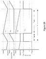
- FIG. 2B is a signal diagram showing voltages and currents developed in the Buck-type drive circuit of FIG. 2A during the critical conduction mode of operation.
- FIG. 3B is a signal diagram showing voltages and currents developed in the SEPIC-type drive circuit of FIG. 3A during the critical conduction mode of operation.
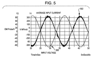
- FIG. 5 is signal diagram showing the phase relationship between the input voltage and average input current across the input capacitors in the drive circuits of FIGS. 2A and 3A .
- FIG. 2A is a circuit diagram illustrating a Buck-type drive circuit 200 for driving a number of series-connected LEDs 202 according to one embodiment of the present invention.
- the converter 200 includes first and second switching transistors Q 1 and Q 2 and a current transducer 204 coupled in series with the second switching transistor Q 2 to generate a voltage feedback signal VFB having a value that is a function of a current IQ 2 flowing through a second switching transistor. Because the current IQ 2 has a value that is functionally related to the value of a drive, load or output current IOUT flowing through the series-connected LEDs 202 , the current IQ 2 may be utilized to control the output current IOUT flowing through the LEDs 202 , as will be explained in more detail below. Using the current IQ 2 enables the drive circuit 200 to control the LEDs 202 through pulse width modulation (PWM) techniques without direct measurement of the output current IOUT through the LEDs, as will also be described in more detail below.
- PWM pulse width modulation
- the error amplifier 210 receives a reference voltage REF on a non-inverting input and operates to integrate the difference between the AVG signal and the reference signal and generate a corresponding error signal ER.
- the error signal ER is output to a PWM modulator 212 which uses this error signal to generate complementary pulse width modulated control output signals OUT, OUT* to control the turning ON and OFF of the switching transistors Q 1 and Q 2 .
- PWM modulator 212 uses this error signal to generate complementary pulse width modulated control output signals OUT, OUT* to control the turning ON and OFF of the switching transistors Q 1 and Q 2 .
- the drive circuit 200 uses average current supplied to the output capacitor COUT to regulate the load or output current IOUT supplied to the series-connected LEDs 202 . More specifically, during each cycle of the drive circuit 200 , the switching current IQ 2 through the transistor Q 2 is sensed by the current transducer 204 , where a cycle corresponds to an ON/OFF period of the switching transistor Q 1 , as will be discussed in more detail below. During an ON duration of each cycle, the switching current IQ 2 flows through the transistor Q 2 and is sensed by the current transducer 204 , which develops the voltage feedback signal FB having a value that is a function of this switching current.
- the detector circuit 206 In response to the voltage feedback signal FB, the detector circuit 206 generates the average current signal AVG indicating the average value of the switching current IQ 2 during this cycle or ON/OFF period of the transistor Q.
- the switching current IQ 2 will have a triangular shape and thus the detector circuit 206 may either provide a peak of this triangular wave form and divide this peak value by two, in the case of critical conduction mose operation, to generate the average current signal or may perform actual averaging of the switching current to generate the average current signal.
- suitable circuitry for forming the detector circuit 206 will understand suitable circuitry for forming the detector circuit 206 .
- FIG. 2B is a signal diagram showing voltages and currents developed in the Buck-type drive circuit 200 of FIG. 2A during the critical conduction mode of operation.
- the diagram shows, for one cycle of the driver circuit 200 , the waveforms for the current IL 1 flowing through the inductor L 1 and the switching currents IQ 1 and IQ 2 flowing through the switching transistors Q 1 and Q 2 , along with the output voltage VOUT across the capacitor COUT.
- the output current IOUT delivered to the load is equal to the average current in the inductor L 1 , regardless of mode of operation of the Buck converter (i.e., discontinuous conduction mode (DCM), critical conduction mode (CRCM) or continuous conduction mode (CCM)).
- the average inductor current in L 1 designated ⁇ L1 , can be easily calculated using simple mathematics and found to be:
- the average inductor current can be determined by passing the output of a current transducer 204 in series with L 1 into a low pass filter, such as a resistor-capacitor network or other filter can be used as the detector circuit 206 to yield the AVG signal.
- the current transducer 204 monitors current IL 1 through the inductor IL 1 . In the case of the synchronous Buck converter of FIG. 2A , this technique also applies to DCM operation.
- a sample and hold circuit could, for example, be utilized to sample these currents (i.e., sample the feedback voltage VFB generated by the current transducer 204 sensing these currents) and then sum the two samples and multiply that sum by 0.5 to yield the desired average current value, which corresponds to the output current IOUT.
- suitable hardware circuitry or a combination of hardware and software may be utilized to implement the above equation.
- Such hardware circuitry is likely more costly than measuring the inductor current IL 1 directly, and thus from a pragmatic standpoint operation in the CRCM or CCM modes rather than the DCM may be more desirable.
- the SEPIC type drive circuit 300 includes a single switching transistor Q 1 , two inductive elements L 1 and L 2 , input and output capacitors CIN and COUT, an input voltage source that supplies input voltage VIN, intermediate capacitor C 1 and a diode D 1 interconnected as shown to form an SEPIC type voltage converter.
- a current transducer 304 senses current IL 2 flowing through the inductive element L 2 and generates a feedback voltage signal VFB having a value that is a function of the current IL 2 .
- An averaging or peak detector circuit 306 receives the VFB signal and generates an output signal indicating the average or peak value of the current IL 2 .
- the detector circuit 306 generates an average signal AVG having a value corresponding to the average of the current IL 2 through the inductor element L 2 .
- a PWM controller 308 includes components 310 - 318 that operate in a manner analogous to the corresponding components 210 - 218 previously described with reference to the PWM controller 208 of FIG. 2A .
- output of the NOR gate 318 generates a control output signal OUT is applied to control the activation and deactivation of the switching transistor Q 1 .
- FIGS. 3B-3D are signal diagrams of illustrating the operation of the drive circuit during the CRCM, DCM and CCM modes of operation, respectively.
- the ideal waveforms for the current IL 2 flowing through the inductive element L 2 in the SEPIC converter operating in the CRCM mode are shown in FIG. 3B .
- the current in the inductor L 2 ramps up during a time TON when the switching transistor Q 1 is turned ON and ramps down during a time TOFF 1 when switching transistor Q 1 turned OFF.
- the sum of TON+TOFF 1 once again defines the cycle TS.
- FIG. 3C is a signal diagram illustrating the operation of the SEPIC converter in the drive circuit 300 during the DCM mode of operation.
- the load or output current IOUT is still equal to the average value ⁇ L2 of the inductor current IL 2 flowing in the inductor L 2 and is given by the following equation:
- FIG. 3D is a signal diagram illustrating the operation of the drive circuit 300 in the CCM mode.
- the output current IOUT is still equal to the average value of the inductor current ⁇ L2 flowing in the inductor L 2 during this mode of operation and is given by the following equation:
- the drive circuits 200 / 300 using the switched currents IQ 2 and IL 2 to control the output current IOUT through the LEDs 202 / 302 eliminates the need to monitor this LED current directly.
- the current transducers 204 / 304 can monitor the desired switched current at many locations, but the current being monitored is fundamentally either the inductor current IL or the current through an output diode. As long as the monitored switching current represents the current that flows into the output capacitor COUT, it can be used to control the load current.
- the input voltage VIN may be a rectified AC input source or may be from a DC voltage source.
- Operating the drive circuits 200 / 300 in the CRCM or DCM mode allows convenient monitoring of the output current IOUT supplied to the load presented by the series-connected LEDs 202 / 302 by monitoring the current inductor or switching element current as discussed above.
- the input voltage VIN is a DC voltage
- the circuits can also be operated in the CCM mode.
- the drive circuits 200 / 300 may also be operated in the CCM mode if power factor correction is not required.
- the circuits 200 and 300 shows single switching transistors Q 1 and Q 2 although each of these is generally a switching element that may be formed from a variety of different types of circuits and thus may include more than one transistor along with other components as well. MOS devices are shown for the switching transistors Q 1 and Q 2 but other types of transistors can be utilized as well.
- the LEDs 202 and 302 are shown and described as being series-connected diodes, this is merely intended to represent the load to which the output current IOUT is being supplied. The load represented by the LEDs 202 and 302 would typically include a large number of LEDs that are connected in series and parallel combinations to provide the desired illumination. Therefore, the present invention is to be limited only by the appended claims.
Landscapes
- Circuit Arrangement For Electric Light Sources In General (AREA)
- Dc-Dc Converters (AREA)
Abstract
Description
where IPEAK and IVALLEY are values for the inductor current IL1 as designated in
As seen from this equation, sensing the current through one of the switching elements, Q1 or Q2, to determine the average inductor current requires knowing the duration of each time intervals TON, TOFF1, and TOFF2, which vary with the particular operating conditions of the
where the current IDC is a DC current that varies with the actual operating conditions, and may be either positive, negative, or zero. In the example of
where IDC is once again a DC current that varies with the actual operating conditions and is equal to zero in the example of
Once again, one way of capturing a value for the average inductor current ĪL2 is to provide the VFB signal from the
Claims (27)
Priority Applications (1)
| Application Number | Priority Date | Filing Date | Title |
|---|---|---|---|
| US12/002,611 US7944153B2 (en) | 2006-12-15 | 2007-12-17 | Constant current light emitting diode (LED) driver circuit and method |
Applications Claiming Priority (2)
| Application Number | Priority Date | Filing Date | Title |
|---|---|---|---|
| US87507506P | 2006-12-15 | 2006-12-15 | |
| US12/002,611 US7944153B2 (en) | 2006-12-15 | 2007-12-17 | Constant current light emitting diode (LED) driver circuit and method |
Publications (2)
| Publication Number | Publication Date |
|---|---|
| US20080224625A1 US20080224625A1 (en) | 2008-09-18 |
| US7944153B2 true US7944153B2 (en) | 2011-05-17 |
Family
ID=39761988
Family Applications (1)
| Application Number | Title | Priority Date | Filing Date |
|---|---|---|---|
| US12/002,611 Expired - Fee Related US7944153B2 (en) | 2006-12-15 | 2007-12-17 | Constant current light emitting diode (LED) driver circuit and method |
Country Status (1)
| Country | Link |
|---|---|
| US (1) | US7944153B2 (en) |
Cited By (48)
| Publication number | Priority date | Publication date | Assignee | Title |
|---|---|---|---|---|
| US20090066263A1 (en) * | 2007-08-29 | 2009-03-12 | Sanyo Electric Co., Ltd. | Light Emitting Element Control Circuit |
| US20100091523A1 (en) * | 2007-06-29 | 2010-04-15 | Murata Manufacturing Co., Ltd. | Switching power supply apparatus |
| US20100176740A1 (en) * | 2007-06-22 | 2010-07-15 | Osram Gesellschaft Mit Beschraenkter Haftung | Feedforward control of semiconductor light sources |
| US20100219763A1 (en) * | 2009-02-27 | 2010-09-02 | Osram Gesellschaft Mit Beschraenkter Haftung | Device and method for dimming light sources |
| US20110080110A1 (en) * | 2009-10-07 | 2011-04-07 | Lutron Electronics Co., Inc. | Load control device for a light-emitting diode light source |
| US20110181199A1 (en) * | 2008-12-12 | 2011-07-28 | O2Micro, Inc. | Controllers, systems and methods for controlling dimming of light sources |
| US20110204777A1 (en) * | 2008-08-18 | 2011-08-25 | Switch Bulb Company, Inc. | Settable light bulbs |
| US20110215728A1 (en) * | 2008-08-18 | 2011-09-08 | Switch Bulb Company, Inc. | Constant power led circuit |
| US20110267856A1 (en) * | 2009-01-14 | 2011-11-03 | Nxp B.V. | Pfc with high efficiency at low load |
| US20120049757A1 (en) * | 2010-08-27 | 2012-03-01 | Delta Electronics, Inc. | Ballast control circuit and ballast control method for gas discharge lamp |
| US20120299502A1 (en) * | 2010-03-04 | 2012-11-29 | Yan Tiesheng | Circuits and methods for driving light sources |
| US8378588B2 (en) | 2008-12-12 | 2013-02-19 | O2Micro Inc | Circuits and methods for driving light sources |
| US8378589B2 (en) | 2008-12-12 | 2013-02-19 | O2Micro, Inc. | Driving circuit with dimming controller for driving light sources |
| US8482219B2 (en) | 2008-12-12 | 2013-07-09 | O2Micro, Inc. | Driving circuit with dimming controller for driving light sources |
| US8698419B2 (en) | 2010-03-04 | 2014-04-15 | O2Micro, Inc. | Circuits and methods for driving light sources |
| US20140239810A1 (en) * | 2013-02-28 | 2014-08-28 | Asahi Kasei Microdevices Corporation | Power factor correction converter with current regulated output |
| US20140252950A1 (en) * | 2013-03-07 | 2014-09-11 | Panasonic Corporation | Semiconductor light source lighting circuit and vehicular lamp |
| US8866398B2 (en) | 2012-05-11 | 2014-10-21 | O2Micro, Inc. | Circuits and methods for driving light sources |
| US20150091470A1 (en) * | 2011-04-22 | 2015-04-02 | On-Bright Electronics (Shanghai) Co., Ltd. | Systems and methods for dimming control with capacitive loads |
| US9030122B2 (en) | 2008-12-12 | 2015-05-12 | O2Micro, Inc. | Circuits and methods for driving LED light sources |
| US9232591B2 (en) | 2008-12-12 | 2016-01-05 | O2Micro Inc. | Circuits and methods for driving light sources |
| US9253843B2 (en) | 2008-12-12 | 2016-02-02 | 02Micro Inc | Driving circuit with dimming controller for driving light sources |
| US9301349B2 (en) | 2011-05-11 | 2016-03-29 | On-Bright Electronics (Shanghai) Co., Ltd. | Systems and methods for dimming control using system controllers |
| US9386653B2 (en) | 2008-12-12 | 2016-07-05 | O2Micro Inc | Circuits and methods for driving light sources |
| US9408269B2 (en) | 2012-11-12 | 2016-08-02 | On-Bright Electronics (Shanghai) Co., Ltd. | Systems and methods for dimming control using TRIAC dimmers |
| US9451247B2 (en) | 2013-11-25 | 2016-09-20 | Ul Llc | Camera test apparatus |
| US9480118B2 (en) | 2014-04-25 | 2016-10-25 | Guangzhou On-Bright Electronics Co., Ltd. | Systems and methods for intelligent control related to TRIAC dimmers |
| US9585222B2 (en) | 2014-07-08 | 2017-02-28 | On-Bright Electronics (Shanghai) Co., Ltd. | Systems and methods for intelligent dimming control using TRIAC dimmers |
| RU170312U1 (en) * | 2016-06-10 | 2017-04-21 | Юрий Борисович Соколов | Sequential LED Driver |
| US9883561B1 (en) | 2016-10-17 | 2018-01-30 | Guangzhou On-Bright Electronics Co., Ltd. | Systems and methods for intelligent control related to triac dimmers by using modulation signals |
| US10193442B2 (en) | 2016-02-09 | 2019-01-29 | Faraday Semi, LLC | Chip embedded power converters |
| USRE47402E1 (en) | 2012-09-17 | 2019-05-21 | Energy Focus, Inc. | LED lamp system |
| US10375785B2 (en) | 2017-11-30 | 2019-08-06 | On-Bright Electronics (Shanghai) Co., Ltd. | Systems and methods for stage-based control related to TRIAC dimmers |
| US10504848B1 (en) | 2019-02-19 | 2019-12-10 | Faraday Semi, Inc. | Chip embedded integrated voltage regulator |
| US10512131B2 (en) | 2017-09-14 | 2019-12-17 | On-Bright Electronics (Shanghai) Co., Ltd. | Systems and methods for bleeder control related to lighting emitting diodes |
| US10827588B2 (en) | 2017-12-28 | 2020-11-03 | On-Bright Electronics (Shanghai) Co., Ltd. | LED lighting systems with TRIAC dimmers and methods thereof |
| US11063516B1 (en) | 2020-07-29 | 2021-07-13 | Faraday Semi, Inc. | Power converters with bootstrap |
| US11069624B2 (en) | 2019-04-17 | 2021-07-20 | Faraday Semi, Inc. | Electrical devices and methods of manufacture |
| US11183996B2 (en) | 2017-07-10 | 2021-11-23 | On-Bright Electronics (Shanghai) Co., Ltd. | Switch control systems for light emitting diodes and methods thereof |
| US11216021B2 (en) | 2019-11-25 | 2022-01-04 | Realtek Semiconductor Corporation | Current generation circuit |
| US11224105B2 (en) | 2019-02-19 | 2022-01-11 | On-Bright Electronics (Shanghai) Co., Ltd. | Systems and methods with TRIAC dimmers for voltage conversion related to light emitting diodes |
| US11252799B2 (en) | 2019-12-27 | 2022-02-15 | On-Bright Electronics (Shanghai) Co., Ltd. | Systems and methods for controlling currents flowing through light emitting diodes |
| US11297704B2 (en) | 2019-08-06 | 2022-04-05 | On-Bright Electronics (Shanghai) Co., Ltd. | Systems and methods for bleeder control related to TRIAC dimmers associated with LED lighting |
| US11405992B2 (en) | 2019-11-20 | 2022-08-02 | On-Bright Electronics (Shanghai) Co., Ltd. | Systems and methods for dimming control related to TRIAC dimmers associated with LED lighting |
| US11540371B2 (en) | 2020-04-13 | 2022-12-27 | On-Bright Electronics (Shanghai) Co., Ltd. | Systems and methods for controlling power factors of LED lighting systems |
| US11564299B2 (en) | 2019-12-19 | 2023-01-24 | On-Bright Electronics (Shanghai) Co., Ltd. | Systems and methods for providing power supply to current controllers associated with LED lighting |
| US11990839B2 (en) | 2022-06-21 | 2024-05-21 | Faraday Semi, Inc. | Power converters with large duty cycles |
| US11996770B2 (en) | 2022-11-23 | 2024-05-28 | Faraday Semi, Inc. | Chip embedded power converters |
Families Citing this family (55)
| Publication number | Priority date | Publication date | Assignee | Title |
|---|---|---|---|---|
| US7956831B2 (en) * | 2007-05-30 | 2011-06-07 | Honeywell Interntional Inc. | Apparatus, systems, and methods for dimming an active matrix light-emitting diode (LED) display |
| WO2008144961A1 (en) * | 2007-05-31 | 2008-12-04 | Texas Instruments Incorporated | Regulation for led strings |
| JP2009004156A (en) * | 2007-06-20 | 2009-01-08 | Sharp Corp | Light-emitting element driving circuit for lighting and lighting device equipped with it |
| KR20090058363A (en) * | 2007-12-04 | 2009-06-09 | 삼성전자주식회사 | Display apparatus for compensating optical parameters using forward voltage of led and method thereof |
| US7733030B2 (en) * | 2007-12-26 | 2010-06-08 | Analog Devices, Inc. | Switching power converter with controlled startup mechanism |
| US8022634B2 (en) | 2008-02-05 | 2011-09-20 | Intersil Americas Inc. | Method and system for dimming AC-powered light emitting diode (LED) lighting systems using conventional incandescent dimmers |
| US8203281B2 (en) * | 2008-04-29 | 2012-06-19 | Ivus Industries, Llc | Wide voltage, high efficiency LED driver circuit |
| US9531156B2 (en) * | 2008-06-18 | 2016-12-27 | Versatile Power, Inc. | Endoscopic light source |
| CN101686587B (en) * | 2008-09-25 | 2015-01-28 | 皇家飞利浦电子股份有限公司 | Drive for providing variable power for LED array |
| KR101511189B1 (en) * | 2008-11-18 | 2015-04-13 | 삼성디스플레이 주식회사 | Method of driving a light source, light-source apparatus for performing the method and display apparatus having the light-source appatus |
| KR101539359B1 (en) * | 2009-02-05 | 2015-07-27 | 삼성디스플레이 주식회사 | Method for driving a light source, light source apparatus for performing the method, and display apparatus having the light source apparatus |
| EP2341760A1 (en) | 2009-12-23 | 2011-07-06 | Tridonic AG | Circuit for operating light emitting diodes (LEDs) |
| CN101827480B (en) * | 2010-04-30 | 2014-02-12 | 海洋王照明科技股份有限公司 | LED drive control circuit |
| EP2385747A3 (en) * | 2010-05-08 | 2012-05-16 | EMD Technologies, Inc. | LED illumination systems |
| CN101835312B (en) * | 2010-05-10 | 2014-03-26 | 海洋王照明科技股份有限公司 | LED drive control circuit |
| TWI423728B (en) * | 2010-05-26 | 2014-01-11 | Tpv Electronics Fujian Co Ltd | Driving circuit for single-string light-emitting diode (led) lamp |
| US8476843B2 (en) * | 2011-01-17 | 2013-07-02 | TPV Electronics (Fujian) Co., Ltd. | Driving circuit for single-string LED lamp |
| US8928297B2 (en) | 2011-01-31 | 2015-01-06 | Infineon Technologies Austria Ag | Ćuk based current source |
| US8680787B2 (en) | 2011-03-15 | 2014-03-25 | Lutron Electronics Co., Inc. | Load control device for a light-emitting diode light source |
| EP2695486A2 (en) * | 2011-04-04 | 2014-02-12 | Sgm A/S | Method for driving leds |
| US8476847B2 (en) | 2011-04-22 | 2013-07-02 | Crs Electronics | Thermal foldback system |
| US8669711B2 (en) | 2011-04-22 | 2014-03-11 | Crs Electronics | Dynamic-headroom LED power supply |
| US8669715B2 (en) | 2011-04-22 | 2014-03-11 | Crs Electronics | LED driver having constant input current |
| DE102011100012A1 (en) * | 2011-04-29 | 2012-10-31 | Tridonic Gmbh & Co. Kg | Method and circuit for power factor correction |
| CN102510617B (en) * | 2011-10-26 | 2014-04-23 | 鸿富锦精密工业(深圳)有限公司 | Circuit for adjusting brightness of light emitting diode (LED) |
| US8823284B2 (en) | 2011-11-10 | 2014-09-02 | Honeywell International Inc. | Optimal power supply topologies for switched current-driven LEDs |
| DE102011088966A1 (en) | 2011-12-19 | 2013-06-20 | Tridonic Gmbh & Co. Kg | Operating circuit for light-emitting diodes and method for operating light-emitting diodes |
| US9502980B2 (en) * | 2011-12-27 | 2016-11-22 | Infineon Technologies Americas Corp. | Circuit and method for producing an average output inductor current indicator |
| BE1020014A5 (en) * | 2012-01-27 | 2013-03-05 | Mindcet Bvba | METHODS AND SYSTEM FOR CALCULATING MODEL PARAMETERS FOR A SPOOL TO BE MODELED. |
| CN104272476B (en) * | 2012-05-09 | 2017-10-27 | 松下知识产权经营株式会社 | Light emitting diode drive device and semiconductor device |
| CN104521326B (en) * | 2012-05-28 | 2016-08-31 | 松下知识产权经营株式会社 | Light emitting diode drive device and semiconductor device |
| JP5999326B2 (en) * | 2012-07-05 | 2016-09-28 | パナソニックIpマネジメント株式会社 | LED lighting device and lighting apparatus |
| DE102012111317B4 (en) | 2012-11-23 | 2021-07-22 | HELLA GmbH & Co. KGaA | Circuit arrangement with a step-down converter |
| US9985520B2 (en) * | 2012-12-17 | 2018-05-29 | Continental Automotive Systems, Inc. | Pulse width modulator for DC/DC converters |
| US9735674B2 (en) * | 2012-12-17 | 2017-08-15 | Continental Automotive Systems, Inc. | PWM generation for DC/DC converters with frequency switching |
| AT514028B1 (en) * | 2013-03-07 | 2017-02-15 | Dipl Ing Dr Himmelstoss Felix | Opto driver stages with rapid increase in current in the light-emitting components |
| US9167649B2 (en) * | 2013-08-02 | 2015-10-20 | Panasonic Intellectual Property Management Co., Ltd. | Lighting device and luminaire |
| JP6152736B2 (en) * | 2013-08-02 | 2017-06-28 | パナソニックIpマネジメント株式会社 | Lighting device and lighting apparatus |
| DE102014003405B4 (en) * | 2014-03-07 | 2021-10-21 | Elmos Semiconductor Se | Down-converting LED driver with a mean-value-based control concept for use in vehicles |
| DE102014017308B4 (en) | 2014-03-07 | 2021-01-28 | Elmos Semiconductor Se | Down-converting LED driver with a mean value-based control concept for use in vehicles with a minimum switch-off period |
| US9351352B2 (en) * | 2014-04-03 | 2016-05-24 | Linear Technology Corporation | Boost then floating buck mode converter for LED driver using common switch control signal |
| KR20160011908A (en) * | 2014-07-23 | 2016-02-02 | 주식회사 솔루엠 | Power conveter and driving method for the same |
| US10271390B2 (en) * | 2014-08-25 | 2019-04-23 | Cree, Inc. | Solid-state lighting fixture with compound semiconductor driver circuitry |
| US9844107B2 (en) | 2014-08-25 | 2017-12-12 | Cree, Inc. | High efficiency driver circuitry for a solid state lighting fixture |
| US10187943B2 (en) * | 2015-06-10 | 2019-01-22 | Mosway Semiconductor Ltd. | Direct drive LED lighting |
| US9763291B2 (en) * | 2015-08-19 | 2017-09-12 | Honeywell International Inc. | Single stage power factor corrected LED driver circuit |
| CA3014830A1 (en) * | 2015-12-08 | 2017-06-15 | Eaton Intelligent Power Limited | Constant power supply for thermo-electric cells |
| CN105788525B (en) | 2016-05-30 | 2019-01-22 | 京东方科技集团股份有限公司 | Driving method and its driving circuit, the backlight and display device of LED light group |
| DE102016221398A1 (en) * | 2016-10-31 | 2018-05-03 | Tridonic Gmbh & Co Kg | DOWN TRANSFORMER FOR ONE LIGHT DIODE |
| WO2018086848A1 (en) * | 2016-11-11 | 2018-05-17 | Tridonic Gmbh & Co Kg | Synchronous down-converter for operating one or more illuminants, associated method and operating unit |
| DE102016223998A1 (en) * | 2016-11-11 | 2018-05-17 | Tridonic Gmbh & Co Kg | Synchronous buck converter for operating one or more lamps, associated method and operating device |
| US10284112B2 (en) * | 2017-05-09 | 2019-05-07 | City University Of Hong Kong | Circuit arrangement for use in a power conversion stage and a method of controlling a power conversion stage |
| JP6932347B2 (en) * | 2017-05-31 | 2021-09-08 | 株式会社リコー | Drive circuit and light emitting device |
| US10578654B2 (en) * | 2017-12-29 | 2020-03-03 | Texas Instruments Incorporated | Apparatus and methods for processing sensed current |
| US11013083B2 (en) * | 2019-05-20 | 2021-05-18 | The Research Foundation for the State University | Electrolytic capacitorless, selectively dimmable LED driver |
Citations (8)
| Publication number | Priority date | Publication date | Assignee | Title |
|---|---|---|---|---|
| US5614810A (en) * | 1994-02-14 | 1997-03-25 | Magneteck, Inc. | Power factor correction circuit |
| US5682306A (en) * | 1995-07-31 | 1997-10-28 | Hewlett-Packard Company | Switched mode power supply with power factor correction |
| US6466188B1 (en) * | 2000-01-20 | 2002-10-15 | International Business Machines Corporation | DC-DC converter with current sensing for use with non-linear devices |
| US6596977B2 (en) * | 2001-10-05 | 2003-07-22 | Koninklijke Philips Electronics N.V. | Average light sensing for PWM control of RGB LED based white light luminaries |
| US7202608B2 (en) * | 2004-06-30 | 2007-04-10 | Tir Systems Ltd. | Switched constant current driving and control circuit |
| US20070080911A1 (en) * | 2005-10-11 | 2007-04-12 | Da Liu | Controller circuitry for light emitting diodes |
| US7425803B2 (en) * | 2004-08-31 | 2008-09-16 | Stmicroelectronics, Inc. | Method and circuit for driving a low voltage light emitting diode |
| US7542257B2 (en) * | 2004-09-10 | 2009-06-02 | Philips Solid-State Lighting Solutions, Inc. | Power control methods and apparatus for variable loads |
-
2007
- 2007-12-17 US US12/002,611 patent/US7944153B2/en not_active Expired - Fee Related
Patent Citations (8)
| Publication number | Priority date | Publication date | Assignee | Title |
|---|---|---|---|---|
| US5614810A (en) * | 1994-02-14 | 1997-03-25 | Magneteck, Inc. | Power factor correction circuit |
| US5682306A (en) * | 1995-07-31 | 1997-10-28 | Hewlett-Packard Company | Switched mode power supply with power factor correction |
| US6466188B1 (en) * | 2000-01-20 | 2002-10-15 | International Business Machines Corporation | DC-DC converter with current sensing for use with non-linear devices |
| US6596977B2 (en) * | 2001-10-05 | 2003-07-22 | Koninklijke Philips Electronics N.V. | Average light sensing for PWM control of RGB LED based white light luminaries |
| US7202608B2 (en) * | 2004-06-30 | 2007-04-10 | Tir Systems Ltd. | Switched constant current driving and control circuit |
| US7425803B2 (en) * | 2004-08-31 | 2008-09-16 | Stmicroelectronics, Inc. | Method and circuit for driving a low voltage light emitting diode |
| US7542257B2 (en) * | 2004-09-10 | 2009-06-02 | Philips Solid-State Lighting Solutions, Inc. | Power control methods and apparatus for variable loads |
| US20070080911A1 (en) * | 2005-10-11 | 2007-04-12 | Da Liu | Controller circuitry for light emitting diodes |
Cited By (100)
| Publication number | Priority date | Publication date | Assignee | Title |
|---|---|---|---|---|
| US20100176740A1 (en) * | 2007-06-22 | 2010-07-15 | Osram Gesellschaft Mit Beschraenkter Haftung | Feedforward control of semiconductor light sources |
| US8378583B2 (en) * | 2007-06-22 | 2013-02-19 | Osram Gesellschaft Mit Beschraenkter Haftung | Feedforward control of semiconductor light sources |
| US8274800B2 (en) * | 2007-06-29 | 2012-09-25 | Murata Manufacturing Co., Ltd. | DC-DC switching power supply with power factor correction |
| US20100091523A1 (en) * | 2007-06-29 | 2010-04-15 | Murata Manufacturing Co., Ltd. | Switching power supply apparatus |
| US20090066263A1 (en) * | 2007-08-29 | 2009-03-12 | Sanyo Electric Co., Ltd. | Light Emitting Element Control Circuit |
| US8305006B2 (en) * | 2007-08-29 | 2012-11-06 | Semiconductor Components Industries, Llc | Light emitting element control circuit |
| US8760066B2 (en) * | 2008-08-18 | 2014-06-24 | Switch Bulb Company, Inc. | Constant power LED circuit |
| US20110204777A1 (en) * | 2008-08-18 | 2011-08-25 | Switch Bulb Company, Inc. | Settable light bulbs |
| US20110215728A1 (en) * | 2008-08-18 | 2011-09-08 | Switch Bulb Company, Inc. | Constant power led circuit |
| US9253843B2 (en) | 2008-12-12 | 2016-02-02 | 02Micro Inc | Driving circuit with dimming controller for driving light sources |
| US9030122B2 (en) | 2008-12-12 | 2015-05-12 | O2Micro, Inc. | Circuits and methods for driving LED light sources |
| US9232591B2 (en) | 2008-12-12 | 2016-01-05 | O2Micro Inc. | Circuits and methods for driving light sources |
| US20110181199A1 (en) * | 2008-12-12 | 2011-07-28 | O2Micro, Inc. | Controllers, systems and methods for controlling dimming of light sources |
| US8378588B2 (en) | 2008-12-12 | 2013-02-19 | O2Micro Inc | Circuits and methods for driving light sources |
| US8378589B2 (en) | 2008-12-12 | 2013-02-19 | O2Micro, Inc. | Driving circuit with dimming controller for driving light sources |
| US8508150B2 (en) | 2008-12-12 | 2013-08-13 | O2Micro, Inc. | Controllers, systems and methods for controlling dimming of light sources |
| US9386653B2 (en) | 2008-12-12 | 2016-07-05 | O2Micro Inc | Circuits and methods for driving light sources |
| US8482219B2 (en) | 2008-12-12 | 2013-07-09 | O2Micro, Inc. | Driving circuit with dimming controller for driving light sources |
| US8644041B2 (en) * | 2009-01-14 | 2014-02-04 | Nxp B.V. | PFC with high efficiency at low load |
| US20110267856A1 (en) * | 2009-01-14 | 2011-11-03 | Nxp B.V. | Pfc with high efficiency at low load |
| US20100219763A1 (en) * | 2009-02-27 | 2010-09-02 | Osram Gesellschaft Mit Beschraenkter Haftung | Device and method for dimming light sources |
| US8933639B2 (en) * | 2009-02-27 | 2015-01-13 | Osram Gesellschaft Mit Beschraenkter Haftung | Device and method for dimming light sources |
| US8492987B2 (en) * | 2009-10-07 | 2013-07-23 | Lutron Electronics Co., Inc. | Load control device for a light-emitting diode light source |
| US20110080110A1 (en) * | 2009-10-07 | 2011-04-07 | Lutron Electronics Co., Inc. | Load control device for a light-emitting diode light source |
| US8664895B2 (en) * | 2010-03-04 | 2014-03-04 | O2Micro, Inc. | Circuits and methods for driving light sources |
| US8698419B2 (en) | 2010-03-04 | 2014-04-15 | O2Micro, Inc. | Circuits and methods for driving light sources |
| US20120299502A1 (en) * | 2010-03-04 | 2012-11-29 | Yan Tiesheng | Circuits and methods for driving light sources |
| US8890440B2 (en) | 2010-03-04 | 2014-11-18 | O2Micro, Inc. | Circuits and methods for driving light sources |
| US20120049757A1 (en) * | 2010-08-27 | 2012-03-01 | Delta Electronics, Inc. | Ballast control circuit and ballast control method for gas discharge lamp |
| US8436557B2 (en) * | 2010-08-27 | 2013-05-07 | Delta Electronics, Inc. | Ballast control circuit and ballast control method for gas discharge lamp |
| US20150091470A1 (en) * | 2011-04-22 | 2015-04-02 | On-Bright Electronics (Shanghai) Co., Ltd. | Systems and methods for dimming control with capacitive loads |
| US9414455B2 (en) * | 2011-04-22 | 2016-08-09 | On-Bright Electronics (Shanghai) Co., Ltd. | Systems and methods for dimming control with capacitive loads |
| US10292217B2 (en) | 2011-05-11 | 2019-05-14 | On-Bright Electronics (Shanghai) Co., Ltd. | Systems and methods for dimming control using system controllers |
| US9301349B2 (en) | 2011-05-11 | 2016-03-29 | On-Bright Electronics (Shanghai) Co., Ltd. | Systems and methods for dimming control using system controllers |
| US9554432B2 (en) | 2011-05-11 | 2017-01-24 | On-Bright Electronics (Shanghai) Co., Ltd. | Systems and methods for dimming control using system controllers |
| US8866398B2 (en) | 2012-05-11 | 2014-10-21 | O2Micro, Inc. | Circuits and methods for driving light sources |
| USRE47402E1 (en) | 2012-09-17 | 2019-05-21 | Energy Focus, Inc. | LED lamp system |
| US10999904B2 (en) | 2012-11-12 | 2021-05-04 | On-Bright Electronics (Shanghai) Co., Ltd. | Systems and methods for dimming control using TRIAC dimmers |
| US9408269B2 (en) | 2012-11-12 | 2016-08-02 | On-Bright Electronics (Shanghai) Co., Ltd. | Systems and methods for dimming control using TRIAC dimmers |
| US10448470B2 (en) | 2012-11-12 | 2019-10-15 | On-Bright Electronics (Shanghai) Co., Ltd. | Systems and methods for dimming control using triac dimmers |
| US10455657B2 (en) | 2012-11-12 | 2019-10-22 | On-Bright Electronics (Shanghai) Co., Ltd. | Systems and methods for dimming control using TRIAC dimmers |
| US9961734B2 (en) | 2012-11-12 | 2018-05-01 | On-Bright Electronics (Shanghai) Co., Ltd. | Systems and methods for dimming control using TRIAC dimmers |
| US10194500B2 (en) | 2012-11-12 | 2019-01-29 | On-Bright Electronics (Shanghai) Co., Ltd. | Systems and methods for dimming control using TRIAC dimmers |
| US20140239810A1 (en) * | 2013-02-28 | 2014-08-28 | Asahi Kasei Microdevices Corporation | Power factor correction converter with current regulated output |
| US8884548B2 (en) * | 2013-02-28 | 2014-11-11 | Asahi Kasei Microdevices Corporation | Power factor correction converter with current regulated output |
| US20140252950A1 (en) * | 2013-03-07 | 2014-09-11 | Panasonic Corporation | Semiconductor light source lighting circuit and vehicular lamp |
| US8970136B2 (en) * | 2013-03-07 | 2015-03-03 | Panasonic Corporation | Semiconductor light source lighting circuit and vehicular lamp |
| US9451247B2 (en) | 2013-11-25 | 2016-09-20 | Ul Llc | Camera test apparatus |
| US9480118B2 (en) | 2014-04-25 | 2016-10-25 | Guangzhou On-Bright Electronics Co., Ltd. | Systems and methods for intelligent control related to TRIAC dimmers |
| US11212885B2 (en) | 2014-04-25 | 2021-12-28 | Guangzhou On-Bright Electronics Co., Ltd. | Systems and methods for intelligent control related to TRIAC dimmers |
| US10383187B2 (en) | 2014-04-25 | 2019-08-13 | Guangzhou On-Bright Electronics Co., Ltd. | Systems and methods for intelligent control related to TRIAC dimmers |
| US9585222B2 (en) | 2014-07-08 | 2017-02-28 | On-Bright Electronics (Shanghai) Co., Ltd. | Systems and methods for intelligent dimming control using TRIAC dimmers |
| US10334677B2 (en) | 2014-07-08 | 2019-06-25 | On-Bright Electronics (Shanghai) Co., Ltd. | Systems and methods for intelligent dimming control using TRIAC dimmers |
| US10342087B2 (en) | 2014-07-08 | 2019-07-02 | On-Bright Electronics (Shanghai) Co., Ltd. | Systems and methods for intelligent dimming control using TRIAC dimmers |
| US10448469B2 (en) | 2014-07-08 | 2019-10-15 | On-Bright Electronics (Shanghai) Co., Ltd. | Systems and methods for intelligent dimming control using TRIAC dimmers |
| US9750107B2 (en) | 2014-07-08 | 2017-08-29 | On-Bright Electronics (Shanghai) Co., Ltd. | Systems and methods for intelligent dimming control using TIRAC dimmers |
| US10687397B2 (en) | 2014-07-08 | 2020-06-16 | On-Bright Electronics (Shanghai) Co., Ltd. | Systems and methods for intelligent dimming control using TRIAC dimmers |
| US9883562B2 (en) | 2014-07-08 | 2018-01-30 | On-Bright Electronics (Shanghai) Co., Ltd. | Systems and methods for intelligent dimming control using TRIAC dimmers |
| US11557962B2 (en) | 2016-02-09 | 2023-01-17 | Faraday Semi, Inc. | Chip embedded power converters |
| US10924011B2 (en) | 2016-02-09 | 2021-02-16 | Faraday Semi, Inc. | Chip embedded power converters |
| US10193442B2 (en) | 2016-02-09 | 2019-01-29 | Faraday Semi, LLC | Chip embedded power converters |
| RU170312U1 (en) * | 2016-06-10 | 2017-04-21 | Юрий Борисович Соколов | Sequential LED Driver |
| US10264642B2 (en) | 2016-10-17 | 2019-04-16 | Guangzhou On-Bright Electronics Co., Ltd. | Systems and methods for intelligent control related to TRIAC dimmers by using modulation signals |
| US9883561B1 (en) | 2016-10-17 | 2018-01-30 | Guangzhou On-Bright Electronics Co., Ltd. | Systems and methods for intelligent control related to triac dimmers by using modulation signals |
| US11201612B2 (en) | 2017-07-10 | 2021-12-14 | On-Bright Electronics (Shanghai) Co., Ltd. | Switch control systems for light emitting diodes and methods thereof |
| US11183996B2 (en) | 2017-07-10 | 2021-11-23 | On-Bright Electronics (Shanghai) Co., Ltd. | Switch control systems for light emitting diodes and methods thereof |
| US11784638B2 (en) | 2017-07-10 | 2023-10-10 | On-Bright Electronics (Shanghai) Co., Ltd. | Switch control systems for light emitting diodes and methods thereof |
| US11695401B2 (en) | 2017-07-10 | 2023-07-04 | On-Bright Electronics (Shanghai) Co., Ltd. | Switch control systems for light emitting diodes and methods thereof |
| US11206015B2 (en) | 2017-07-10 | 2021-12-21 | On-Bright Electronics (Shanghai) Co., Ltd. | Switch control systems for light emitting diodes and methods thereof |
| US10512131B2 (en) | 2017-09-14 | 2019-12-17 | On-Bright Electronics (Shanghai) Co., Ltd. | Systems and methods for bleeder control related to lighting emitting diodes |
| US10973095B2 (en) | 2017-09-14 | 2021-04-06 | On-Bright Electronics (Shanghai) Co., Ltd. | Systems and methods for bleeder control related to lighting emitting diodes |
| US10375785B2 (en) | 2017-11-30 | 2019-08-06 | On-Bright Electronics (Shanghai) Co., Ltd. | Systems and methods for stage-based control related to TRIAC dimmers |
| US11026304B2 (en) | 2017-11-30 | 2021-06-01 | On-Bright Electronics (Shanghai) Co., Ltd. | Systems and methods for stage-based control related to TRIAC dimmers |
| US10999903B2 (en) | 2017-11-30 | 2021-05-04 | On-Bright Electronics (Shanghai) Co., Ltd. | Systems and methods for stage-based control related to TRIAC dimmers |
| US10785837B2 (en) | 2017-11-30 | 2020-09-22 | On-Bright Electronics (Shanghai) Co., Ltd. | Systems and methods for stage-based control related to TRIAC dimmers |
| US11937350B2 (en) | 2017-12-28 | 2024-03-19 | On-Bright Electronics (Shanghai) Co., Ltd. | LED lighting systems with TRIAC dimmers and methods thereof |
| US10827588B2 (en) | 2017-12-28 | 2020-11-03 | On-Bright Electronics (Shanghai) Co., Ltd. | LED lighting systems with TRIAC dimmers and methods thereof |
| US11638335B2 (en) | 2017-12-28 | 2023-04-25 | On-Bright Electronics (Shanghai) Co., Ltd. | LED lighting systems with TRIAC dimmers and methods thereof |
| US11570859B2 (en) | 2017-12-28 | 2023-01-31 | On-Bright Electronics (Shanghai) Co., Ltd. | LED lighting systems with TRIAC dimmers and methods thereof |
| US11224105B2 (en) | 2019-02-19 | 2022-01-11 | On-Bright Electronics (Shanghai) Co., Ltd. | Systems and methods with TRIAC dimmers for voltage conversion related to light emitting diodes |
| US10504848B1 (en) | 2019-02-19 | 2019-12-10 | Faraday Semi, Inc. | Chip embedded integrated voltage regulator |
| US11652062B2 (en) | 2019-02-19 | 2023-05-16 | Faraday Semi, Inc. | Chip embedded integrated voltage regulator |
| US11678417B2 (en) | 2019-02-19 | 2023-06-13 | On-Bright Electronics (Shanghai) Co., Ltd. | Systems and methods with TRIAC dimmers for voltage conversion related to light emitting diodes |
| US11069624B2 (en) | 2019-04-17 | 2021-07-20 | Faraday Semi, Inc. | Electrical devices and methods of manufacture |
| US11621230B2 (en) | 2019-04-17 | 2023-04-04 | Faraday Semi, Inc. | Electrical devices and methods of manufacture |
| US11297704B2 (en) | 2019-08-06 | 2022-04-05 | On-Bright Electronics (Shanghai) Co., Ltd. | Systems and methods for bleeder control related to TRIAC dimmers associated with LED lighting |
| US11792901B2 (en) | 2019-08-06 | 2023-10-17 | On-Bright Electronics (Shanghai) Co., Ltd. | Systems and methods for bleeder control related to TRIAC dimmers associated with LED lighting |
| US11405992B2 (en) | 2019-11-20 | 2022-08-02 | On-Bright Electronics (Shanghai) Co., Ltd. | Systems and methods for dimming control related to TRIAC dimmers associated with LED lighting |
| US11743984B2 (en) | 2019-11-20 | 2023-08-29 | On-Bright Electronics (Shanghai) Co., Ltd. | Systems and methods for dimming control related to TRIAC dimmers associated with LED lighting |
| US11216021B2 (en) | 2019-11-25 | 2022-01-04 | Realtek Semiconductor Corporation | Current generation circuit |
| US11564299B2 (en) | 2019-12-19 | 2023-01-24 | On-Bright Electronics (Shanghai) Co., Ltd. | Systems and methods for providing power supply to current controllers associated with LED lighting |
| US11856670B2 (en) | 2019-12-19 | 2023-12-26 | On-Bright Electronics (Shanghai) Co., Ltd. | Systems and methods for providing power supply to current controllers associated with LED lighting |
| US11723128B2 (en) | 2019-12-27 | 2023-08-08 | On-Bright Electronics (Shanghai) Co., Ltd. | Systems and methods for controlling currents flowing through light emitting diodes |
| US11252799B2 (en) | 2019-12-27 | 2022-02-15 | On-Bright Electronics (Shanghai) Co., Ltd. | Systems and methods for controlling currents flowing through light emitting diodes |
| US11540371B2 (en) | 2020-04-13 | 2022-12-27 | On-Bright Electronics (Shanghai) Co., Ltd. | Systems and methods for controlling power factors of LED lighting systems |
| US11997772B2 (en) | 2020-04-13 | 2024-05-28 | On-Bright Electronics (Shanghai) Co., Ltd. | Systems and methods for controlling power factors of led lighting systems |
| US11063516B1 (en) | 2020-07-29 | 2021-07-13 | Faraday Semi, Inc. | Power converters with bootstrap |
| US11855534B2 (en) | 2020-07-29 | 2023-12-26 | Faraday Semi, Inc. | Power converters with bootstrap |
| US11990839B2 (en) | 2022-06-21 | 2024-05-21 | Faraday Semi, Inc. | Power converters with large duty cycles |
| US11996770B2 (en) | 2022-11-23 | 2024-05-28 | Faraday Semi, Inc. | Chip embedded power converters |
Also Published As
| Publication number | Publication date |
|---|---|
| US20080224625A1 (en) | 2008-09-18 |
Similar Documents
| Publication | Publication Date | Title |
|---|---|---|
| US7944153B2 (en) | Constant current light emitting diode (LED) driver circuit and method | |
| US8213194B2 (en) | Control device for a flyback converter | |
| EP2536013B1 (en) | A cascade boost and inverting buck converter | |
| EP2248249B1 (en) | Electronic driver circuit and method | |
| EP3066535B1 (en) | Method and apparatus for calculating an average value of an inaccessible current from an acessible current | |
| EP2135487B1 (en) | Lighting system with power factor correction control data determined from a phase modulated signal | |
| US7538534B2 (en) | Method and apparatus for controlling output current of a cascaded DC/DC converter | |
| TWI508613B (en) | High efficiency LED driver circuit and its driving method | |
| CN202652596U (en) | Circuit for controlling dimming level of one or more light emitting diodes | |
| US7880400B2 (en) | Digital driver apparatus, method and system for solid state lighting | |
| US8587209B2 (en) | LED drivers and control methods | |
| US8400123B2 (en) | Voltage converter and voltage conversion method | |
| US20090015178A1 (en) | LED driver and control method thereof | |
| US9491819B2 (en) | Hysteretic power factor control method for single stage power converters | |
| US20120327690A1 (en) | Primary-Side Based Control Of Econdary-Side Current For A Transformer | |
| EP2389046A2 (en) | Triac dimmer compatible switching mode power supply and the method thereof | |
| US9913332B2 (en) | Two-channel LED driver and the control method thereof | |
| USRE44406E1 (en) | Method of detecting switching power supply output current | |
| US20120268023A1 (en) | Circuits and methods for driving light sources | |
| JP2016529871A5 (en) | ||
| JP2004186159A (en) | Lighting device | |
| JP6279749B2 (en) | LED driver and control method | |
| JP2014075875A (en) | Dc power supply device | |
| GB2497213A (en) | Circuits and methods for driving light sources | |
| EP3139483A1 (en) | Electronic reverse buck converter, and corresponding method of operating an electronic reverse buck converter |
Legal Events
| Date | Code | Title | Description |
|---|---|---|---|
| AS | Assignment |
Owner name: INTERSIL AMERICAS INC., CALIFORNIA Free format text: ASSIGNMENT OF ASSIGNORS INTEREST;ASSIGNOR:GREENFIELD, FRED;REEL/FRAME:020315/0397 Effective date: 20071215 |
|
| AS | Assignment |
Owner name: MORGAN STANLEY & CO. INCORPORATED,NEW YORK Free format text: SECURITY AGREEMENT;ASSIGNORS:INTERSIL CORPORATION;TECHWELL, INC.;INTERSIL COMMUNICATIONS, INC.;AND OTHERS;REEL/FRAME:024329/0411 Effective date: 20100427 Owner name: MORGAN STANLEY & CO. INCORPORATED, NEW YORK Free format text: SECURITY AGREEMENT;ASSIGNORS:INTERSIL CORPORATION;TECHWELL, INC.;INTERSIL COMMUNICATIONS, INC.;AND OTHERS;REEL/FRAME:024329/0411 Effective date: 20100427 |
|
| STCF | Information on status: patent grant |
Free format text: PATENTED CASE |
|
| CC | Certificate of correction | ||
| AS | Assignment |
Owner name: INTERSIL AMERICAS LLC, CALIFORNIA Free format text: CHANGE OF NAME;ASSIGNOR:INTERSIL AMERICAS INC.;REEL/FRAME:033119/0484 Effective date: 20111223 |
|
| FPAY | Fee payment |
Year of fee payment: 4 |
|
| FEPP | Fee payment procedure |
Free format text: MAINTENANCE FEE REMINDER MAILED (ORIGINAL EVENT CODE: REM.); ENTITY STATUS OF PATENT OWNER: LARGE ENTITY |
|
| LAPS | Lapse for failure to pay maintenance fees |
Free format text: PATENT EXPIRED FOR FAILURE TO PAY MAINTENANCE FEES (ORIGINAL EVENT CODE: EXP.); ENTITY STATUS OF PATENT OWNER: LARGE ENTITY |
|
| STCH | Information on status: patent discontinuation |
Free format text: PATENT EXPIRED DUE TO NONPAYMENT OF MAINTENANCE FEES UNDER 37 CFR 1.362 |
|
| FP | Lapsed due to failure to pay maintenance fee |
Effective date: 20190517 |