EP3139483A1 - Electronic reverse buck converter, and corresponding method of operating an electronic reverse buck converter - Google Patents
Electronic reverse buck converter, and corresponding method of operating an electronic reverse buck converter Download PDFInfo
- Publication number
- EP3139483A1 EP3139483A1 EP16178841.9A EP16178841A EP3139483A1 EP 3139483 A1 EP3139483 A1 EP 3139483A1 EP 16178841 A EP16178841 A EP 16178841A EP 3139483 A1 EP3139483 A1 EP 3139483A1
- Authority
- EP
- European Patent Office
- Prior art keywords
- error signal
- err
- current
- signal
- voltage
- Prior art date
- Legal status (The legal status is an assumption and is not a legal conclusion. Google has not performed a legal analysis and makes no representation as to the accuracy of the status listed.)
- Withdrawn
Links
Images


Classifications
-
- H—ELECTRICITY
- H02—GENERATION; CONVERSION OR DISTRIBUTION OF ELECTRIC POWER
- H02M—APPARATUS FOR CONVERSION BETWEEN AC AND AC, BETWEEN AC AND DC, OR BETWEEN DC AND DC, AND FOR USE WITH MAINS OR SIMILAR POWER SUPPLY SYSTEMS; CONVERSION OF DC OR AC INPUT POWER INTO SURGE OUTPUT POWER; CONTROL OR REGULATION THEREOF
- H02M3/00—Conversion of dc power input into dc power output
- H02M3/02—Conversion of dc power input into dc power output without intermediate conversion into ac
- H02M3/04—Conversion of dc power input into dc power output without intermediate conversion into ac by static converters
- H02M3/10—Conversion of dc power input into dc power output without intermediate conversion into ac by static converters using discharge tubes with control electrode or semiconductor devices with control electrode
- H02M3/145—Conversion of dc power input into dc power output without intermediate conversion into ac by static converters using discharge tubes with control electrode or semiconductor devices with control electrode using devices of a triode or transistor type requiring continuous application of a control signal
- H02M3/155—Conversion of dc power input into dc power output without intermediate conversion into ac by static converters using discharge tubes with control electrode or semiconductor devices with control electrode using devices of a triode or transistor type requiring continuous application of a control signal using semiconductor devices only
- H02M3/156—Conversion of dc power input into dc power output without intermediate conversion into ac by static converters using discharge tubes with control electrode or semiconductor devices with control electrode using devices of a triode or transistor type requiring continuous application of a control signal using semiconductor devices only with automatic control of output voltage or current, e.g. switching regulators
- H02M3/1563—Conversion of dc power input into dc power output without intermediate conversion into ac by static converters using discharge tubes with control electrode or semiconductor devices with control electrode using devices of a triode or transistor type requiring continuous application of a control signal using semiconductor devices only with automatic control of output voltage or current, e.g. switching regulators without using an external clock
-
- H—ELECTRICITY
- H05—ELECTRIC TECHNIQUES NOT OTHERWISE PROVIDED FOR
- H05B—ELECTRIC HEATING; ELECTRIC LIGHT SOURCES NOT OTHERWISE PROVIDED FOR; CIRCUIT ARRANGEMENTS FOR ELECTRIC LIGHT SOURCES, IN GENERAL
- H05B45/00—Circuit arrangements for operating light-emitting diodes [LED]
- H05B45/10—Controlling the intensity of the light
-
- H—ELECTRICITY
- H05—ELECTRIC TECHNIQUES NOT OTHERWISE PROVIDED FOR
- H05B—ELECTRIC HEATING; ELECTRIC LIGHT SOURCES NOT OTHERWISE PROVIDED FOR; CIRCUIT ARRANGEMENTS FOR ELECTRIC LIGHT SOURCES, IN GENERAL
- H05B45/00—Circuit arrangements for operating light-emitting diodes [LED]
- H05B45/30—Driver circuits
- H05B45/37—Converter circuits
- H05B45/3725—Switched mode power supply [SMPS]
- H05B45/375—Switched mode power supply [SMPS] using buck topology
-
- H—ELECTRICITY
- H02—GENERATION; CONVERSION OR DISTRIBUTION OF ELECTRIC POWER
- H02M—APPARATUS FOR CONVERSION BETWEEN AC AND AC, BETWEEN AC AND DC, OR BETWEEN DC AND DC, AND FOR USE WITH MAINS OR SIMILAR POWER SUPPLY SYSTEMS; CONVERSION OF DC OR AC INPUT POWER INTO SURGE OUTPUT POWER; CONTROL OR REGULATION THEREOF
- H02M1/00—Details of apparatus for conversion
- H02M1/0083—Converters characterised by their input or output configuration
- H02M1/009—Converters characterised by their input or output configuration having two or more independently controlled outputs
Definitions
- the description relates to electronic converters.
- This disclosure was devised with specific attention paid to the improvement of the driving of an electronic reverse buck (or inverse buck) converter.
- Electronic converters for light sources comprising e.g. at least one LED (Light Emitting Diode) or other solid-state lighting means, may offer a direct current output. Such current may be steady or vary in time, e.g. in order to adjust the brightness emitted by the light source (so-called dimming function).
- LED Light Emitting Diode
- dimming function the dimming function
- Figure 1 shows a possible lighting arrangement comprising an electronic converter 10 and a lighting module 20 including, for instance, at least one LED 202.
- Figure 2 shows an example of a lighting module 20 comprising, e.g., a LED chain, i.e. a plurality of LEDs connected in series.
- a lighting module 20 comprising, e.g., a LED chain, i.e. a plurality of LEDs connected in series.
- Figure 2 shows four LEDs L 1 , L 2 , L 3 e L 4 .
- Electronic converter 10 often comprises a control circuit 102 and a power circuit 12 (e.g. an AC/DC or DC/DC switching supply) which receives at an input a supply signal (e.g. from the mains) and provides at an output, through a power output 106, a direct current.
- a supply signal e.g. from the mains
- a direct current e.g. from the mains
- control circuit 102 may set, via a reference channel I ref of power circuit 12, the current requested by LED module 20.
- such a reference channel I ref may be used in order to adjust the brightness of the light emitted by lighting module 20.
- a regulation of the light brightness emitted by LED module 20 may be achieved by regulating the average current flowing through the lighting module, for example by setting a lower reference current I ref or by switching on or off power circuit 12 through a Pulse Width Modulation (PWM) signal, typically at a low frequency, e.g. between 50 and 500 Hz.
- PWM Pulse Width Modulation
- Figure 3 shows a circuit diagram of a buck converter operating as a DC/DC converter.
- an input alternated current (AC) may be converted into a direct current (DC) via a rectifier, e.g. a diode-bridge rectifier, and optionally a filter capacitor.
- a further DC/DC converter might be provided between the rectifier and the filter capacitor, e.g. a PFC (Power Factor Correction) converter which further stabilizes the voltage at the filter capacitor and/or improves the power factor.
- a PFC Power Factor Correction
- a buck converter comprises an electronic switch S, a diode D, an inductor L and often a capacitor C.
- converter 12 receives at input, via two input terminals 110, a voltage V in and provides at output, via two output terminals 106, a regulated voltage V o or a regulated current i o .
- the first terminal (positive terminal) of input 110 is connected, via switch S, to a first terminal of inductor L, and the second terminal (negative terminal) of input 110 represents a ground GND.
- the second terminal of inductor L is connected to the first terminal (positive terminal) of output 106, and the second terminal (negative terminal) of output 106 is connected to ground GND.
- the cathode of diode D which may generally be implemented also as a second switch, is connected at the middle point between switch S and inductor L, and the anode of diode D is connected to ground GND.
- capacitor C is connected in parallel with output 106, i.e. directly to output terminals 106. Generally speaking, such a capacitor C may be omitted in the case of a current control.
- a load R L is connected to said output 106, and it may consist of the previously described lighting module 20.
- control may be a voltage or a current control.
- a control unit 112 is typically provided which drives switch S so that output voltage V o or output current i o is set to a desired value, e.g. reference current I ref .
- a sensor may be provided which is adapted to detect current i o or voltage V o .
- switch S is closed and diode D is off, i.e. diode D has a reverse bias.
- inductor L saves the energy received from input 110.
- the current flowing through inductor L has a substantially linear increase, while no current flows through diode D.
- both previously described operating periods are periodically repeated with a fixed frequency, wherein energy transfer is controlled via a PWM signal; in other words, the duration of the first and of the second period varies, while the sum of the durations is constant.
- Figure 5 shows an alternative embodiment of a buck converter, wherein the arrangement of switch S and of inductor L is different.
- this topology is named reverse buck (or inverse buck) converter.
- the first terminal of input 110 is directly connected to the first output terminal.
- the second terminal of input 110 which represents ground GND, is connected through switch S to a first terminal of inductor L.
- the second terminal of inductor L is connected to the second output terminal 106.
- the anode of diode D which also in this topology may be implemented as a second switch, is connected at the middle point between switch S and inductor L, and the cathode of diode D is connected to the first terminal of input 110 or to the first terminal of output 106.
- a capacitor C may be connected in parallel with output 106, i.e. directly to output terminals 106.
- switch S is no longer connected to the positive input terminal, but to the negative terminal.
- switch S is now a "low-side" switch and may be implemented, e.g., as an N-MOS transistor.
- inductor L has changed, because it is sufficient to have inductor L connected in series with output 106.
- the paper “ NCL30100 - Fixed Off Time Switched Mode LED Driver Controller", Semiconductor Components Industries, LLC, 2011 , the content whereof is included herein as a reference, describes a control circuit for a reverse buck converter, which is used for driving at least one LED.
- this paper proposes using the "negative current sensing" technology (see for instance Figure 15 of the paper) in order to measure, via a shunt resistor R CS , the current flowing through the LEDs.
- said shunt resistor R CS is connected between the second output terminal and switch S, and may therefore only indicate the current traversing switch S, and not necessarily the current which actually flows through the LEDs.
- the object of the invention is to overcome the previously outlined drawbacks.
- the present description refers to embodiments of electronic reverse buck converters.
- the converter comprises two input terminals, which receive a first supply signal, and two output terminals which provide a second supply signal, wherein the second input terminal represents a first ground and the second output terminal represents a second ground.
- the converter comprises moreover a diode and an electronic switch, which are connected in series between the input terminals, wherein the cathode of the diode is connected to the first input terminal and the switch is connected between the second input terminal and the anode of the diode.
- the converter also comprises an inductor, wherein the inductor and both output terminals are connected in series between the cathode and the anode of the diode.
- the first output terminal may be connected to the cathode of the diode
- the inductor may be connected to the anode of the diode.
- the electronic converter also comprises a shunt resistor and a control circuit.
- the shunt resistor is connected between the second output terminal and the inductor, so that the voltage across the shunt resistor is indicative of the current being provided through output terminals (106).
- control circuit comprises an error amplifier, adapted to generate a first error signal as a function of the voltage across the shunt resistor, and an identified reference signal of a requested current.
- the first error signal is referred to the second ground, i.e. the output ground. Therefore, in various embodiments, the control circuit comprises a voltage conversion circuit (level shifter), adapted to receive the first error signal and to generate a second error signal indicating the value of the first error signal, wherein the second error signal is referred to the first, i.e. the input ground.
- a voltage conversion circuit level shifter
- control circuit comprises a driver circuit, adapted to drive the switching of the electronic switch as a function of the second error signal.
- the error signal is a binary signal, wherein the error amplifier is adapted to set the error signal to a first logic value when the current being provided through the output terminals should be increased, and to set the error signal to a second logic value when the current should be decreased.
- an error amplifier may be implemented as a comparator or as a comparator with hysteresis.
- the error amplifier is a regulator comprising a P (proportional) portion, so that the error signal comprises a ripple which is proportional to the difference between the requested current and the current being provided through the output terminals.
- the driver circuit may be implemented directly as a comparator with hysteresis.
- the error amplifier in order to improve the accuracy of the control-loop regulator, preferably comprises an I (integral) portion, so that the average value of the error signal either increases or decreases until the current being provided through the output terminals matches in average the requested current.
- the voltage conversion circuit comprises a current generator, generating a current as a function of the first error signal, and a voltage generator generating the second error signal as a function of such current.
- the reference signal is provided by a detection circuit, which receives information identifying the requested current through a communication line.
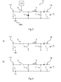
- Figure 6 shows an embodiment of a reverse buck converter 12a according to the present description.
- such a reverse buck converter may be used to supply power to a lighting module 20 comprising one or more LEDs 202.
- converter 12a corresponds to the structure shown with reference to Figure 5 . Therefore, also the converter according to the present description comprises an electronic switch S, a diode D, an inductor L, optionally a capacitor C and a control unit 112a, wherein converter 12a receives as input, through two input terminals 110, a DC voltage V in and provides as output, through two output terminals 106, a regulated voltage V o or preferably a regulated current i o .
- the first terminal (positive terminal) of input 110 is connected (e.g. directly) to the cathode of diode D, and the second terminal (negative terminal) of input 110, representing a first ground GNDA, is connected through switch S to the anode of diode D. Therefore, in the presently considered embodiment, switch S is connected to ground GNDA and may be implemented as an N-MOS transistor.
- diode D is a Schottky diode.
- diode D may be implemented as another type of diode or as a second electronic switch driven by control unit 112, so that this switch and switch S are closed alternatively (see for example Figures 4a and 4b ).
- the first terminal (positive terminal) of output 106 is connected (e.g. directly) to the cathode of diode D
- the second terminal (negative terminal) of output 106 is connected (e.g. directly) to the cathode of diode D.
- one or more lighting modules 20 comprising one or more LEDs 202 connected in series and/or in parallel, i.e. one or more LEDs are connected between output terminals 106.
- the voltage across resistor R S corresponds to a signal 114 which is proportional to the current flowing through lighting module(s) 20; in other words, signal 114 is indicative of the current flowing through LEDs 202.
- the arrangement described with reference to Figure 6 offers the advantage that the voltage at the second output terminal, representing a second ground GNDB, has a substantially constant voltage in comparison with the first ground GNDA. Indeed, voltage V o between output terminals 106 substantially corresponds to the sum of the voltages across the LEDs, i.e. of the forward voltages of LEDs 202. Therefore, the voltage at the second output terminal with reference to ground GNDA substantially corresponds to: V in ⁇ V o .
- control circuit 112a is adapted to detect the current flowing through LEDs 202 (in other words, control circuit 112a receives signal 114), and to drive switch S, e.g. an N-MOS transistor, as a function of the detected current; i.e., control circuit 112a provides a drive signal 116 connected to the control terminal of electronic switch S, e.g. to the gate of an N-MOS transistor.
- Figure 7 shows a possible embodiment of control circuit 112a.
- control circuit 112a comprises a regulator 1120, adapted to compare the current traversing LEDs 202 with a reference value REF, e.g. signal I Ref described with reference to Figure 1 .
- Regulator 1120 may be for example a P (proportional) controller, a PI (proportional-integral) controller or a PID (proportional-integral-derivative) controller, and it is normally known as an error amplifier.
- regulator 1120 is adapted to generate an error signal ERR as a function of a signal 114 identified by current i o flowing through LEDs 202 and a reference value REF.
- error signal ERR is sent to a driver circuit 1124, which controls the switching of switch S as a function of error signal ERR.
- regulator 1120 operates with ground GNDB
- driver circuit 1124 operates with ground GNDA
- ERR error signal
- drive signal 116 is referred to ground GNDA
- control circuit 112a comprises a voltage conversion circuit (level shifter) 1122, which converts error signal ERR into a corresponding error signal ERR' referred to ground GNDA, i.e. voltage conversion circuit 1122 receives as input the error signal ERR referred to ground GNDB and provides as output the error signal ERR' referred to mass GNDB.
- voltage conversion circuit 1122 receives as input the error signal ERR referred to ground GNDB and provides as output the error signal ERR' referred to mass GNDB.
- Figure 8 shows a second embodiment, wherein reference signal REF is determined as a function of an ID element 204 provided in lighting module 20.
- control circuit 112a is adapted to communicate with ID element 204, and it adapts the operation of the electronic converter to the operating conditions requested by the LED module.
- control circuit 112a may comprise a detection circuit 1126, adapted to communicate with ID element 204 through a communication line 118 (and ground GNDB).
- circuit 1126 and element 204 may be based on a digital communication protocol, such as a communication with the I 2 C (Inter Integrated Circuit) protocol or another "single wire" or analogue communication protocol.
- a digital communication protocol such as a communication with the I 2 C (Inter Integrated Circuit) protocol or another "single wire” or analogue communication protocol.
- ID element 204 may be a resistor R SET (or another impedance element) connected between line 118 and the second output terminal (e.g. ground GNDB), wherein the impedance value indicates the value of the control parameter, e.g. the requested current.
- R SET resistor SET
- the resistance may be variable.
- detection circuit 1026 may be adapted to apply a voltage to line 118 and detect the current flowing through resistor R SET .
- Figure 10 shows a possible embodiment of the detection circuit, substantially corresponding to Figure 5 of PCT/IB2013/055106 .
- detection circuit 1126 comprises an operational amplifier OpAmp1, wherein the negative input is connected to communication line 118 (line CL in PCT/IB2013/055106 ).
- the output generates a measure signal V REF (voltage Vout in PCT/IB2013/055106 ) provided at the output of detection circuit 1126.
- a current measuring resistor Rfb is connected between the output and the negative input of operational amplifier OpAmp1, thus generating the negative feedback thereof.
- a voltage source Vk is connected between the positive input of operational amplifier OpAmp1 and the ground line GNBD, thus producing the voltage reference for line 118.
- operational amplifier OpAmp1 sets voltage Vk on line 118, and the output provides a voltage V REF which is proportional to the current flowing through line 118; in other words, the detection circuit generates a voltage identifying the requested current.
- this voltage V REF is referred to ground GNDB, because the ground of operational amplifier OpAmp1 is (directly) connected to ground GNDB.
- the supply to operational amplifier OpAmp1 may be provided by line 110, or optionally by an additional voltage regulator, e.g. a converter, providing a 12V voltage.
- detection circuit 1126 may comprise further components, e.g. in order to protect the circuit from an overvoltage on line 118, and/or filters adapted to stabilize measure signal V REF .
- detection circuit 1026 provides a reference signal REF which is indicative of the current requested by lighting module 20.
- such a signal is provided to a regulator 1120, which generates an error signal ERR.
- an error signal ERR is referred to ground GNDB.
- various embodiments envisage the provision of voltage conversion circuit 1122, which may also be implemented as an optical coupler.
- the voltage between ground GNDB and ground GNDA is substantially constant and corresponds to V in - V o . Therefore an expensive optical coupler is not necessary; on the contrary, a level shifter CC may be used.
- voltage conversion circuit 1122 depends on the implementation of regulator 1120 and of driver circuit 1124.
- regulator 1120 In a first embodiment, regulator 1120 generates an error signal ERR with two possible levels: a first logic level, e.g. "1", indicating that the detected current is not sufficient, and a second level, e.g. "0", indicating that the detected current is sufficient.
- a first logic level e.g. "1”
- a second level e.g. "0”
- a regulator 1120 may be implemented e.g. as a comparator with hysteresis.
- Figure 11 shows a possible embodiment of the behaviour of said regulator 1120.
- driver circuit 1124 detects this change, too, and closes switch S.
- driver circuit 1124 may also directly transmit the changes in error signal ERR' to switch S. In the simplest situation, driver circuit 1124 may therefore apply error signal ERR' directly to switch S.
- driver circuit 1124 preferably comprises a so-called gate driver, which typically comprises a comparator or a comparator with hysteresis, such as a Schmitt trigger.
- this embodiment offers the advantage of admitting a less accurate voltage conversion circuit 1122, because it may suffice for the voltage conversion circuit 1122 to be adapted to transmit the information about the level of error signal ERR.
- FIG 12 shows a possible embodiment of regulator 1120.
- reference voltage V REF is summed to voltage V S across shunt resistor R S , which however is negative with respect to ground GNDB.
- the sum of voltages V REF + V S is applied to a voltage divider comprising two connected resistors R 1 and R 2 connected in series. Therefore, in the presently considered embodiment, the middle point 1128 of voltage divider R 1 and R 2 provides a voltage which indicates the difference between the requested current REF and the detected current 114.
- such voltage at the output 1128 of the voltage divider is compared, via a comparator with hysteresis CMP, with a given threshold voltage V TH .
- a threshold voltage V TH should substantially correspond to the voltage being applied to output 1128 when the detected current 114 corresponds to the requested current REF (irrespective of the actual values of voltages V REF and V S ) .
- the error signal ERR provided by comparator CMP will correspond to what is shown in Figure 11 .
- another type of regulator REG is provided in the place of comparator CMP.
- Figure 13 shows an embodiment wherein regulator REG is a P regulator, amplifying the difference between reference signal REF and detected current 114.
- error signal ERR is no longer a binary signal, but a continuous signal indicating the difference between reference signal REF and measured current 114.
- This error signal ERR is converted, via voltage conversion circuit 1122, into an error signal ERR' referred to ground GNDA, and driver circuit 1124 drives switch S as a function of error signal ERR'.
- driver circuit may be a comparator with hysteresis, which compares error signal ERR' with an upper threshold THH and a lower threshold THL. For example, in the presently considered embodiment, when error signal ERR' reaches upper threshold THH, the driver circuit switches signal 116 off and opens switch S, and when error signal ERR' reaches lower threshold THL, the driver circuit switches signal 116 on and closes switch S. As a consequence, in the presently considered embodiment, error signal ERR contains a ripple of the detected current, and this ripple enables to generate drive signal 116 through a comparator with hysteresis and optionally a gate driver.
- this embodiment has substantially the same performance as the embodiment described with reference to Figure 11 , the difference being that the comparator with hysteresis is included in the driver circuit, while regulator 1120 only generates an error signal ERR indicative of the difference between reference signal REF and the detected current 114.
- regulator 1120 e.g. regulator REG shown in Figure 13
- regulator REG is a PI (or optionally a PID) regulator
- the driver circuit is implemented in the same way as the second embodiment, as a comparator with hysteresis.
- error signal ERR comprises a component ERR I , which thanks to the I portion of the regulator is increased or decreased until the desired current is achieved.
- error signal ERR comprises a component ERR P , which thanks to the P portion of the regulator comprises, as in the previous embodiment, a ripple indicative of the difference between the detected and the requested current. Therefore, this embodiment has a performance substantially corresponding to the previous embodiment, the difference being that the average value ERR I of the error signal is determined by the I portion of regulator 1120, i.e. regulator 1120 generates an error signal ERR which is increased or decreased until detected current 114 corresponds (in average) to reference value REF.
- Figure 16 shows a possible embodiment of such a PI regulator through an operational amplifier OpAmp2.
- the negative input of operational amplifier OpAmp2 is connected, through a resistor R A2 , to line 1128 identifying the difference between reference signal REF and the detected current.
- the output generates error signal ERR.
- a resistor R A1 and a capacitor C A1 are connected between the output and the negative input of operational amplifier OpAmp2, thus providing the negative feedback thereof.
- a voltage source V TH is connected to the positive input of operational amplifier OpAmp2, thus providing the reference for the regulator.
- error signal ERR is converted, via voltage conversion circuit 1122, into an error signal ERR' referred to ground GNDA, and driver circuit 1124 drives switch S as a function of error signal ERR'.
- the driver circuit compares error signal ERR' with an upper threshold THH and a lower threshold THL. For example, in the presently considered embodiment, when error signal ERR' reaches upper threshold THH, the driver circuit switches signal 116 off and opens switch S, and when error signal ERR' reaches lower threshold THL, the driver circuit activates signal 116 and closes switch S.
- This embodiment offers the advantage that a possible offset introduced by voltage conversion circuit 1122 is automatically compensated for by the I portion of regulator 1120.
- regulator 1120 e.g. regulator REG shown in Figure 13
- driver circuit 1124 is a PWM driver circuit.
- regulator 1120 provides an error signal ERR which is increased or decreased until the measured current 114 corresponds in average to reference value REF.
- error signal ERR is converted by voltage conversion circuit 1122 into an error signal ERR' referred to ground GNDA, and driver circuit 1124 drives switch S as a function of error signal ERR'.
- driver circuit 1126 receives error signal ERR' and varies the duty cycle of drive signal 116 which drives the switching of switch S as a function of error signal ERR', e.g. it increases the duty cycle when the value of error signal ERR rises.
- regulator 1120 e.g. regulator REG shown in Figure 13
- driver circuit 1124 is a PWM driver circuit with current peak regulation and constant frequency.
- error signal ERR may behave as shown in Figure 15c .
- driver circuit PWM 1124 may synchronize error signal ERR' shown in Figure 15d with a fixed-frequency clock signal. For example, in this case, driver circuit may close switch S with fixed frequency, and may open switch S when error signal ERR or shifted error signal ERR' indicates that the measured current 114 has reached a given upper threshold, e.g. when error signal ERR' reaches upper threshold THH.
- voltage conversion circuit 1122 converts error signal ERR into a corresponding error signal ERR' referred to ground GNDA. Moreover, such signals are actually only shifted for a substantially constant voltage, and therefore voltage conversion circuit 1122 may be implemented more easily. Generally speaking, the main purpose of circuit 1122 is therefore shifting the reference to a different ground. However, in general terms also a manipulation of the signal width might take place.
- error signal ERR may have different characteristics.
- regulator 1122 it is sufficient for voltage conversion circuit 1122 to ensure a proportionality between input signal ERR and output signal ERR'.
- no high accuracy (also as regards offset) or temperature stability are demanded for voltage conversion circuit 1124, because it is sufficient for output signal ERR' to follow only an increase or decrease in the input error signal.
- a substantially linear behaviour between error signal ERR and error signal ERR' may suffice, but it is not necessary to ensure a particular accuracy in level reduction or offset and/or a proportionality between the input signal and the output signal.
- regulator 1120 will increase or decrease error signal ERR until the measured current 114 corresponds to reference signal REF.
- regulator 1120 did not comprise an I portion, e.g. if regulator 1120 were merely a P regulator.
- Figure 15 shows a related embodiment of a voltage conversion circuit 1122.
- circuit 1122 comprises a current generator 1130, which generates a current i c as a function of the input voltage, i.e. of error signal ERR referred to ground GNDB.
- such a current generator 1130 may be implemented as a resistor R 3 and a bipolar pnp transistor Q1.
- resistor R 3 is connected between the emitter of transistor Q1 and a supply voltage V SUP , e.g. 12 V.
- V SUP supply voltage
- the base of transistor Q1 is connected to error signal ERR and the collector provides current i c .
- the person skilled in the art will appreciate that the structure of such a current generator 1130 may also be more complex, and mat comprise one or more current mirrors.
- circuit 1122 moreover comprises a voltage generator 1132, which again converts current i c provided by current generator 1130 into a voltage, or generates signal ERR' as a function of current i c .
- such a circuit 1132 may be implemented as a resistor R 4 connected to ground GNDA. Therefore, in the considered embodiment, the voltage across resistor R 4 , i.e. signal ERR', is proportional to current i c provided by generator 1130.
Landscapes
- Engineering & Computer Science (AREA)
- Power Engineering (AREA)
- Dc-Dc Converters (AREA)
Abstract
Description
- The description relates to electronic converters.
- This disclosure was devised with specific attention paid to the improvement of the driving of an electronic reverse buck (or inverse buck) converter.
- Electronic converters for light sources, comprising e.g. at least one LED (Light Emitting Diode) or other solid-state lighting means, may offer a direct current output. Such current may be steady or vary in time, e.g. in order to adjust the brightness emitted by the light source (so-called dimming function).
-
Figure 1 shows a possible lighting arrangement comprising anelectronic converter 10 and alighting module 20 including, for instance, at least oneLED 202. - For instance,
Figure 2 shows an example of alighting module 20 comprising, e.g., a LED chain, i.e. a plurality of LEDs connected in series. As an example,Figure 2 shows four LEDs L1, L2, L3 e L4. -
Electronic converter 10 often comprises acontrol circuit 102 and a power circuit 12 (e.g. an AC/DC or DC/DC switching supply) which receives at an input a supply signal (e.g. from the mains) and provides at an output, through apower output 106, a direct current. Such a current may be steady or vary in time. For example,control circuit 102 may set, via a reference channel Iref ofpower circuit 12, the current requested byLED module 20. - For example, such a reference channel Iref may be used in order to adjust the brightness of the light emitted by
lighting module 20. Actually, in general terms, a regulation of the light brightness emitted byLED module 20 may be achieved by regulating the average current flowing through the lighting module, for example by setting a lower reference current Iref or by switching on or offpower circuit 12 through a Pulse Width Modulation (PWM) signal, typically at a low frequency, e.g. between 50 and 500 Hz. - In general there are known many types of electronic converters, which are mainly divided into insulated and non-insulated converters. For example, among the non-insulated electronic converters we may name "buck", "boost", "buck-boost", "Cuk", "SEPIC" and "ZETA" converters. Insulated converters are e.g. "flyback", "forward", "Half-bridge" and "Full-bridge" converters. Such converter arrangements are well known to the person skilled in the art.
- For example,
Figure 3 shows a circuit diagram of a buck converter operating as a DC/DC converter. The person skilled in the art will appreciate that an input alternated current (AC) may be converted into a direct current (DC) via a rectifier, e.g. a diode-bridge rectifier, and optionally a filter capacitor. Generally speaking, a further DC/DC converter might be provided between the rectifier and the filter capacitor, e.g. a PFC (Power Factor Correction) converter which further stabilizes the voltage at the filter capacitor and/or improves the power factor. - Substantially, a buck converter comprises an electronic switch S, a diode D, an inductor L and often a capacitor C.
- In the presently considered example,
converter 12 receives at input, via twoinput terminals 110, a voltage Vin and provides at output, via twooutput terminals 106, a regulated voltage Vo or a regulated current i o. - Specifically, the first terminal (positive terminal) of
input 110 is connected, via switch S, to a first terminal of inductor L, and the second terminal (negative terminal) ofinput 110 represents a ground GND. On the other hand, the second terminal of inductor L is connected to the first terminal (positive terminal) ofoutput 106, and the second terminal (negative terminal) ofoutput 106 is connected to ground GND. In the presently considered example, the cathode of diode D, which may generally be implemented also as a second switch, is connected at the middle point between switch S and inductor L, and the anode of diode D is connected to ground GND. Finally, capacitor C is connected in parallel withoutput 106, i.e. directly tooutput terminals 106. Generally speaking, such a capacitor C may be omitted in the case of a current control. - In the presently considered example, a load RL is connected to said
output 106, and it may consist of the previously describedlighting module 20. - As previously stated, the control may be a voltage or a current control. To this purpose, a
control unit 112 is typically provided which drives switch S so that output voltage Vo or output current io is set to a desired value, e.g. reference current Iref. To this purpose, in a way known in itself, a sensor may be provided which is adapted to detect current io or voltage Vo. - Referring to
Figures 4a and 4b a possible driving of such a buck converter will be described. - Specifically, as shown in
Figure 4a , in a first operating period switch S is closed and diode D is off, i.e. diode D has a reverse bias. In this case, inductor L saves the energy received frominput 110. In this condition, the current flowing through inductor L has a substantially linear increase, while no current flows through diode D. - On the contrary, as shown in
Figure 4b , during a second operating period, switch S is open and diode D is on. As a matter of fact, diode D has a direct bias, because the voltage bias across inductor L is reversed. In this condition, the current flowing through inductor L experiences a substantially linear decrease. - Typically, both previously described operating periods are periodically repeated with a fixed frequency, wherein energy transfer is controlled via a PWM signal; in other words, the duration of the first and of the second period varies, while the sum of the durations is constant.
- The person skilled in the art will appreciate that such a PWM driving and the control of the duration of operating periods are well known and may be implemented, e.g., via a feedback of the output voltage or current through an error amplifier. For example, in the case of current control, the duration of the first period is increased until the (average) output current reaches a predetermined threshold.
-
Figure 5 shows an alternative embodiment of a buck converter, wherein the arrangement of switch S and of inductor L is different. Typically, this topology is named reverse buck (or inverse buck) converter. - In the presently considered example, the first terminal of
input 110 is directly connected to the first output terminal. On the other hand, the second terminal ofinput 110, which represents ground GND, is connected through switch S to a first terminal of inductor L. Moreover, the second terminal of inductor L is connected to thesecond output terminal 106. - In the presently considered example, the anode of diode D, which also in this topology may be implemented as a second switch, is connected at the middle point between switch S and inductor L, and the cathode of diode D is connected to the first terminal of
input 110 or to the first terminal ofoutput 106. - Finally, a capacitor C may be connected in parallel with
output 106, i.e. directly tooutput terminals 106. - Therefore, in the presently considered example switch S is no longer connected to the positive input terminal, but to the negative terminal. As a consequence, switch S is now a "low-side" switch and may be implemented, e.g., as an N-MOS transistor.
- Moreover, the position of inductor L has changed, because it is sufficient to have inductor L connected in series with
output 106. - Thus, the general operating principle is substantially unvaried.
- For example, the paper " NCL30100 - Fixed Off Time Switched Mode LED Driver Controller", Semiconductor Components Industries, LLC, 2011, the content whereof is included herein as a reference, describes a control circuit for a reverse buck converter, which is used for driving at least one LED. Specifically, this paper proposes using the "negative current sensing" technology (see for instance
Figure 15 of the paper) in order to measure, via a shunt resistor RCS, the current flowing through the LEDs. Specifically, said shunt resistor RCS is connected between the second output terminal and switch S, and may therefore only indicate the current traversing switch S, and not necessarily the current which actually flows through the LEDs. - The object of the invention is to overcome the previously outlined drawbacks.
- According to the invention, said object is achieved thanks to an electronic reverse buck converter having the features set forth in the claims that follow. The claims refer moreover to a corresponding method of operating an electronic reverse buck converter.
- The claims are an integral part of the technical teaching provided herein with reference to the present description.
- As previously stated, the present description refers to embodiments of electronic reverse buck converters.
- In various embodiments, the converter comprises two input terminals, which receive a first supply signal, and two output terminals which provide a second supply signal, wherein the second input terminal represents a first ground and the second output terminal represents a second ground. The converter comprises moreover a diode and an electronic switch, which are connected in series between the input terminals, wherein the cathode of the diode is connected to the first input terminal and the switch is connected between the second input terminal and the anode of the diode.
- In various embodiments, the converter also comprises an inductor, wherein the inductor and both output terminals are connected in series between the cathode and the anode of the diode. For example, the first output terminal may be connected to the cathode of the diode, and the inductor may be connected to the anode of the diode.
- In various embodiments, the electronic converter also comprises a shunt resistor and a control circuit.
- In various embodiments, the shunt resistor is connected between the second output terminal and the inductor, so that the voltage across the shunt resistor is indicative of the current being provided through output terminals (106).
- In various embodiments, the control circuit comprises an error amplifier, adapted to generate a first error signal as a function of the voltage across the shunt resistor, and an identified reference signal of a requested current.
- Specifically, in various embodiments, the first error signal is referred to the second ground, i.e. the output ground. Therefore, in various embodiments, the control circuit comprises a voltage conversion circuit (level shifter), adapted to receive the first error signal and to generate a second error signal indicating the value of the first error signal, wherein the second error signal is referred to the first, i.e. the input ground.
- In various embodiments, the control circuit comprises a driver circuit, adapted to drive the switching of the electronic switch as a function of the second error signal.
- For example, in various embodiments the error signal is a binary signal, wherein the error amplifier is adapted to set the error signal to a first logic value when the current being provided through the output terminals should be increased, and to set the error signal to a second logic value when the current should be decreased. For example, such an error amplifier may be implemented as a comparator or as a comparator with hysteresis.
- On the other hand, in other embodiments, the error amplifier is a regulator comprising a P (proportional) portion, so that the error signal comprises a ripple which is proportional to the difference between the requested current and the current being provided through the output terminals. In this case, the driver circuit may be implemented directly as a comparator with hysteresis.
- In various embodiments, in order to improve the accuracy of the control-loop regulator, the error amplifier preferably comprises an I (integral) portion, so that the average value of the error signal either increases or decreases until the current being provided through the output terminals matches in average the requested current.
- This arrangement with a PI (or PID) regulator and a comparator with hysteresis offers the advantage that the voltage conversion circuit may be implemented easily. However, generally speaking, other driver circuits may be used as well.
- For example, in various embodiments, the voltage conversion circuit comprises a current generator, generating a current as a function of the first error signal, and a voltage generator generating the second error signal as a function of such current.
- In various embodiments, the reference signal is provided by a detection circuit, which receives information identifying the requested current through a communication line.
- Various embodiments will now be described, by way of non-limiting example only, with reference to the annexed views, wherein:
-
Figures 1 to 5 have already been described in the foregoing, -
Figure 6 shows a first embodiment of an electronic reverse buck converter according to the present description; -
Figure 7 shows an embodiment of a control circuit for the converter ofFigure 7 ; -
Figure 8 shows a second embodiment of the electronic reverse buck converter according to the present description; -
Figure 9 shows an embodiment of a control circuit for the converter ofFigure 8 ; and -
Figures 10 to 17 show details of the control circuits ofFigures 7 and9 . - In the following description, numerous specific details are given to provide a thorough understanding of the embodiments. The embodiments can be practiced without one or more of the specific details, or with other methods, components, materials, etc. In other instances, well-known structures, materials, or operations are not shown or described in detail to avoid obscuring aspects of the embodiments.
- Reference throughout this specification to "one embodiment" or "an embodiment" means that a particular feature, structure, or characteristic described in connection with the embodiment is included in at least one embodiment. Thus, the appearances of the phrases "in one embodiment" or "in an embodiment" in various places throughout this specification are not necessarily all referring to the same embodiment. Furthermore, the particular features, structures, or characteristics may be combined in any suitable manner in one or more embodiments.
- The headings provided herein are for convenience only and do not interpret the extent of protection or meaning of the embodiments.
- In the following
Figures 6 and17 , the parts, elements or components which have already been described with reference toFigures 1 to 5 are denoted with the same references previously used in such Figures; the description of such previously described elements will not be repeated, so as not to overburden the present detailed description. -
Figure 6 shows an embodiment of areverse buck converter 12a according to the present description. - Generally, as described in the introductory section, such a reverse buck converter may be used to supply power to a
lighting module 20 comprising one ormore LEDs 202. - The general structure of
converter 12a corresponds to the structure shown with reference toFigure 5 . Therefore, also the converter according to the present description comprises an electronic switch S, a diode D, an inductor L, optionally a capacitor C and acontrol unit 112a, whereinconverter 12a receives as input, through twoinput terminals 110, a DC voltage Vin and provides as output, through twooutput terminals 106, a regulated voltage Vo or preferably a regulated current io . - Specifically, in the presently considered embodiment, the first terminal (positive terminal) of
input 110 is connected (e.g. directly) to the cathode of diode D, and the second terminal (negative terminal) ofinput 110, representing a first ground GNDA, is connected through switch S to the anode of diode D. Therefore, in the presently considered embodiment, switch S is connected to ground GNDA and may be implemented as an N-MOS transistor. - In the presently considered embodiment, diode D is a Schottky diode. However, in general, diode D may be implemented as another type of diode or as a second electronic switch driven by
control unit 112, so that this switch and switch S are closed alternatively (see for exampleFigures 4a and 4b ). - In the presently considered embodiment, between the cathode and the anode of diode D there are connected the terminals of
output 106, inductor L and a shunt resistor RS. Generally speaking, it is sufficient for the terminals ofoutput 106, inductor L and shunt resistor RS to be connected in series between the cathode and the anode of diode D. - For example, in the presently considered embodiment, the first terminal (positive terminal) of
output 106 is connected (e.g. directly) to the cathode of diode D, the second terminal (negative terminal) ofoutput 106 is connected (e.g. directly) to the cathode of diode D. - In the presently considered embodiment, between
output terminals 106 there are connected one ormore lighting modules 20, comprising one ormore LEDs 202 connected in series and/or in parallel, i.e. one or more LEDs are connected betweenoutput terminals 106. - Therefore, in general, the voltage across resistor RS corresponds to a
signal 114 which is proportional to the current flowing through lighting module(s) 20; in other words, signal 114 is indicative of the current flowing throughLEDs 202. - The arrangement described with reference to
Figure 6 offers the advantage that the voltage at the second output terminal, representing a second ground GNDB, has a substantially constant voltage in comparison with the first ground GNDA. Indeed, voltage Vo betweenoutput terminals 106 substantially corresponds to the sum of the voltages across the LEDs, i.e. of the forward voltages ofLEDs 202. Therefore, the voltage at the second output terminal with reference to ground GNDA substantially corresponds to:
- In the presently considered embodiment,
control circuit 112a is adapted to detect the current flowing through LEDs 202 (in other words,control circuit 112a receives signal 114), and to drive switch S, e.g. an N-MOS transistor, as a function of the detected current; i.e.,control circuit 112a provides adrive signal 116 connected to the control terminal of electronic switch S, e.g. to the gate of an N-MOS transistor. - For example,
Figure 7 shows a possible embodiment ofcontrol circuit 112a. - In the presently considered embodiment,
control circuit 112a comprises aregulator 1120, adapted to compare thecurrent traversing LEDs 202 with a reference value REF, e.g. signal IRef described with reference toFigure 1 .Regulator 1120 may be for example a P (proportional) controller, a PI (proportional-integral) controller or a PID (proportional-integral-derivative) controller, and it is normally known as an error amplifier. - Generally speaking,
regulator 1120 is adapted to generate an error signal ERR as a function of asignal 114 identified by current io flowing throughLEDs 202 and a reference value REF. - In an embodiment, error signal ERR is sent to a
driver circuit 1124, which controls the switching of switch S as a function of error signal ERR. - In an embodiment,
regulator 1120 operates with ground GNDB, whiledriver circuit 1124 operates with ground GNDA, i.e. error signal ERR is referred to ground GNDB and drivesignal 116 is referred to ground GNDA. - Therefore, in an embodiment,
control circuit 112a comprises a voltage conversion circuit (level shifter) 1122, which converts error signal ERR into a corresponding error signal ERR' referred to ground GNDA, i.e.voltage conversion circuit 1122 receives as input the error signal ERR referred to ground GNDB and provides as output the error signal ERR' referred to mass GNDB. -
Figure 8 shows a second embodiment, wherein reference signal REF is determined as a function of anID element 204 provided inlighting module 20. - For example, such an
ID element 204 may identify the current requested by lighting module 20 (or in general control parameters). Therefore, generally speaking,control circuit 112a is adapted to communicate withID element 204, and it adapts the operation of the electronic converter to the operating conditions requested by the LED module. - To this purpose, for example, as shown in
Figure 9 ,control circuit 112a may comprise adetection circuit 1126, adapted to communicate withID element 204 through a communication line 118 (and ground GNDB). - Generally speaking, the communication between
circuit 1126 andelement 204 may be based on a digital communication protocol, such as a communication with the I2C (Inter Integrated Circuit) protocol or another "single wire" or analogue communication protocol. - For example, in the simplest of cases,
ID element 204 may be a resistor RSET (or another impedance element) connected betweenline 118 and the second output terminal (e.g. ground GNDB), wherein the impedance value indicates the value of the control parameter, e.g. the requested current. In general, another resistive element may be used, and/or the resistance may be variable. - For example, for the case wherein the ID element comprises a resistive element, e.g. a resistor RSET, detection circuit 1026 may be adapted to apply a voltage to
line 118 and detect the current flowing through resistor RSET. - Such a technique is described e.g. in
PCT/IB2013/055106 WO 2014/001987 ) andDE 102012224349 A1 , the contents whereof are included in the present description by way of reference. - For example,
Figure 10 shows a possible embodiment of the detection circuit, substantially corresponding toFigure 5 ofPCT/IB2013/055106 - In the presently considered embodiment,
detection circuit 1126 comprises an operational amplifier OpAmp1, wherein the negative input is connected to communication line 118 (line CL inPCT/IB2013/055106 PCT/IB2013/055106 detection circuit 1126. A current measuring resistor Rfb is connected between the output and the negative input of operational amplifier OpAmp1, thus generating the negative feedback thereof. A voltage source Vk is connected between the positive input of operational amplifier OpAmp1 and the ground line GNBD, thus producing the voltage reference forline 118. - Therefore, in the present arrangement operational amplifier OpAmp1 sets voltage Vk on
line 118, and the output provides a voltage VREF which is proportional to the current flowing throughline 118; in other words, the detection circuit generates a voltage identifying the requested current. Specifically, this voltage VREF is referred to ground GNDB, because the ground of operational amplifier OpAmp1 is (directly) connected to ground GNDB. On the other end, the supply to operational amplifier OpAmp1 may be provided byline 110, or optionally by an additional voltage regulator, e.g. a converter, providing a 12V voltage. The person skilled in the art will appreciate thatdetection circuit 1126 may comprise further components, e.g. in order to protect the circuit from an overvoltage online 118, and/or filters adapted to stabilize measure signal VREF . - An alternative solution is described in
EP 2014/170495 EP 2 814 302 A1 ), wherein the ID element is a shunt regulator or a Zener diode limiting the voltage online 118. - Therefore, in various embodiments, detection circuit 1026 provides a reference signal REF which is indicative of the current requested by
lighting module 20. - As previously stated, such a signal is provided to a
regulator 1120, which generates an error signal ERR. According to various embodiments, such an error signal ERR is referred to ground GNDB. - Therefore, various embodiments envisage the provision of
voltage conversion circuit 1122, which may also be implemented as an optical coupler. However, as previously stated, the voltage between ground GNDB and ground GNDA is substantially constant and corresponds to Vin - Vo. Therefore an expensive optical coupler is not necessary; on the contrary, a level shifter CC may be used. - The implementation of
voltage conversion circuit 1122 depends on the implementation ofregulator 1120 and ofdriver circuit 1124. - In a first embodiment,
regulator 1120 generates an error signal ERR with two possible levels: a first logic level, e.g. "1", indicating that the detected current is not sufficient, and a second level, e.g. "0", indicating that the detected current is sufficient. For example, such aregulator 1120 may be implemented e.g. as a comparator with hysteresis. -
Figure 11 shows a possible embodiment of the behaviour of saidregulator 1120. - Specifically, when switch S is off, detected current 114 increases (see
Figure 11a ). When the detected current 114 reaches an upper threshold (seeFigure 11b ), e.g. REF + TH, the output ofcomparator 1120 switches the logic level, e.g. error signal ERR is set to "0".Driver circuit 1124 detects this change and opens switch S (seeFigure 11c ). - Now the detected current 114 decreases. When the detected current 114 reaches a lower threshold, e.g. REF - TH, the output of comparator 112' switches logic level again. In the presently considered embodiment,
driver circuit 1124 detects this change, too, and closes switch S. - As a consequence, in the presently considered embodiment,
driver circuit 1124 may also directly transmit the changes in error signal ERR' to switch S. In the simplest situation,driver circuit 1124 may therefore apply error signal ERR' directly to switch S. However,driver circuit 1124 preferably comprises a so-called gate driver, which typically comprises a comparator or a comparator with hysteresis, such as a Schmitt trigger. - Therefore, this embodiment offers the advantage of admitting a less accurate
voltage conversion circuit 1122, because it may suffice for thevoltage conversion circuit 1122 to be adapted to transmit the information about the level of error signal ERR. - In this situation
Figure 12 shows a possible embodiment ofregulator 1120. - In the presently considered embodiment, reference voltage VREF is summed to voltage VS across shunt resistor RS, which however is negative with respect to ground GNDB. The sum of voltages VREF + VS is applied to a voltage divider comprising two connected resistors R1 and R2 connected in series. Therefore, in the presently considered embodiment, the
middle point 1128 of voltage divider R1 and R2 provides a voltage which indicates the difference between the requested current REF and the detected current 114. - In the presently considered embodiments, such voltage at the
output 1128 of the voltage divider is compared, via a comparator with hysteresis CMP, with a given threshold voltage VTH . Specifically, such a threshold voltage VTH should substantially correspond to the voltage being applied tooutput 1128 when the detected current 114 corresponds to the requested current REF (irrespective of the actual values of voltages VREF and VS ). As a consequence, with an appropriate sizing of resistors R1, R2 and RS and of voltage VTH, the error signal ERR provided by comparator CMP will correspond to what is shown inFigure 11 . - However, the inventors have observed that this solution may lead to accuracy issues in the output current, because the shifting of a digital signal adapted to directly control the gate of switch S may involve problems of delay, generated by
shifter 1122 on the signal switching fronts. - Therefore, in an embodiment, another type of regulator REG is provided in the place of comparator CMP.
- For example,
Figure 13 shows an embodiment wherein regulator REG is a P regulator, amplifying the difference between reference signal REF and detected current 114. - For example, as shown in
Figure 14 , specifically inFigure 14c , error signal ERR is no longer a binary signal, but a continuous signal indicating the difference between reference signal REF and measured current 114. - This error signal ERR is converted, via
voltage conversion circuit 1122, into an error signal ERR' referred to ground GNDA, anddriver circuit 1124 drives switch S as a function of error signal ERR'. - For example, in the presently considered embodiment, driver circuit may be a comparator with hysteresis, which compares error signal ERR' with an upper threshold THH and a lower threshold THL. For example, in the presently considered embodiment, when error signal ERR' reaches upper threshold THH, the driver circuit switches signal 116 off and opens switch S, and when error signal ERR' reaches lower threshold THL, the driver circuit switches signal 116 on and closes switch S. As a consequence, in the presently considered embodiment, error signal ERR contains a ripple of the detected current, and this ripple enables to generate
drive signal 116 through a comparator with hysteresis and optionally a gate driver. - Therefore, this embodiment has substantially the same performance as the embodiment described with reference to
Figure 11 , the difference being that the comparator with hysteresis is included in the driver circuit, whileregulator 1120 only generates an error signal ERR indicative of the difference between reference signal REF and the detected current 114. - In an embodiment,
regulator 1120, e.g. regulator REG shown inFigure 13 , is a PI (or optionally a PID) regulator, and the driver circuit is implemented in the same way as the second embodiment, as a comparator with hysteresis. - For example, as shown in
Figure 15 , specifically inFigure 15c , error signal ERR comprises a component ERRI, which thanks to the I portion of the regulator is increased or decreased until the desired current is achieved. Moreover, error signal ERR comprises a component ERRP, which thanks to the P portion of the regulator comprises, as in the previous embodiment, a ripple indicative of the difference between the detected and the requested current. Therefore, this embodiment has a performance substantially corresponding to the previous embodiment, the difference being that the average value ERRI of the error signal is determined by the I portion ofregulator 1120, i.e.regulator 1120 generates an error signal ERR which is increased or decreased until detected current 114 corresponds (in average) to reference value REF. - For example,
Figure 16 shows a possible embodiment of such a PI regulator through an operational amplifier OpAmp2. - Specifically, in the presently considered embodiment, the negative input of operational amplifier OpAmp2 is connected, through a resistor RA2, to
line 1128 identifying the difference between reference signal REF and the detected current. The output generates error signal ERR. A resistor RA1 and a capacitor CA1 are connected between the output and the negative input of operational amplifier OpAmp2, thus providing the negative feedback thereof. A voltage source VTH is connected to the positive input of operational amplifier OpAmp2, thus providing the reference for the regulator. - Also in this case, error signal ERR is converted, via
voltage conversion circuit 1122, into an error signal ERR' referred to ground GNDA, anddriver circuit 1124 drives switch S as a function of error signal ERR'. - For example, in the presently considered embodiment, the driver circuit compares error signal ERR' with an upper threshold THH and a lower threshold THL. For example, in the presently considered embodiment, when error signal ERR' reaches upper threshold THH, the driver circuit switches signal 116 off and opens switch S, and when error signal ERR' reaches lower threshold THL, the driver circuit activates signal 116 and closes switch S.
- This embodiment offers the advantage that a possible offset introduced by
voltage conversion circuit 1122 is automatically compensated for by the I portion ofregulator 1120. - In one
embodiment regulator 1120, e.g. regulator REG shown inFigure 13 , is an I regulator anddriver circuit 1124 is a PWM driver circuit. - Therefore, in the
present embodiment regulator 1120 provides an error signal ERR which is increased or decreased until the measured current 114 corresponds in average to reference value REF. - In this case as well, error signal ERR is converted by
voltage conversion circuit 1122 into an error signal ERR' referred to ground GNDA, anddriver circuit 1124 drives switch S as a function of error signal ERR'. - For example, in an embodiment,
driver circuit 1126 receives error signal ERR' and varies the duty cycle ofdrive signal 116 which drives the switching of switch S as a function of error signal ERR', e.g. it increases the duty cycle when the value of error signal ERR rises. - In an
embodiment regulator 1120, e.g. regulator REG shown inFigure 13 , is a P regulator (or preferably a PI or PID regulator), anddriver circuit 1124 is a PWM driver circuit with current peak regulation and constant frequency. - Therefore, in this embodiment, error signal ERR may behave as shown in
Figure 15c . - In this case,
driver circuit PWM 1124 may synchronize error signal ERR' shown inFigure 15d with a fixed-frequency clock signal. For example, in this case, driver circuit may close switch S with fixed frequency, and may open switch S when error signal ERR or shifted error signal ERR' indicates that the measured current 114 has reached a given upper threshold, e.g. when error signal ERR' reaches upper threshold THH. - Implementation of the Voltage Conversion Circuit
- As previously described,
voltage conversion circuit 1122 converts error signal ERR into a corresponding error signal ERR' referred to ground GNDA. Moreover, such signals are actually only shifted for a substantially constant voltage, and thereforevoltage conversion circuit 1122 may be implemented more easily. Generally speaking, the main purpose ofcircuit 1122 is therefore shifting the reference to a different ground. However, in general terms also a manipulation of the signal width might take place. - Moreover, according to the implementations of
regulator 1120 and ofdriver circuit 1124, error signal ERR may have different characteristics. - For example, in the solutions employing a regulator with I portion (e.g. an I, PI or PID regulator), it is sufficient for
voltage conversion circuit 1122 to ensure a proportionality between input signal ERR and output signal ERR'. However, no high accuracy (also as regards offset) or temperature stability are demanded forvoltage conversion circuit 1124, because it is sufficient for output signal ERR' to follow only an increase or decrease in the input error signal. For this reason, a substantially linear behaviour between error signal ERR and error signal ERR' may suffice, but it is not necessary to ensure a particular accuracy in level reduction or offset and/or a proportionality between the input signal and the output signal. Indeed, thanks to the closed-loop control,regulator 1120 will increase or decrease error signal ERR until the measured current 114 corresponds to reference signal REF. - On the other hand, a
voltage conversion circuit 1122 with higher accuracy would be required ifregulator 1120 did not comprise an I portion, e.g. ifregulator 1120 were merely a P regulator. -
Figure 15 shows a related embodiment of avoltage conversion circuit 1122. - In the considered embodiment,
circuit 1122 comprises acurrent generator 1130, which generates a current ic as a function of the input voltage, i.e. of error signal ERR referred to ground GNDB. - For example, such a
current generator 1130 may be implemented as a resistor R3 and a bipolar pnp transistor Q1. Specifically, in the presently considered embodiment, resistor R3 is connected between the emitter of transistor Q1 and a supply voltage VSUP, e.g. 12 V. The base of transistor Q1 is connected to error signal ERR and the collector provides current ic. The person skilled in the art will appreciate that the structure of such acurrent generator 1130 may also be more complex, and mat comprise one or more current mirrors. - In the presently considered embodiment,
circuit 1122 moreover comprises avoltage generator 1132, which again converts current ic provided bycurrent generator 1130 into a voltage, or generates signal ERR' as a function of current ic . - For example, in the simplest of cases, such a
circuit 1132 may be implemented as a resistor R4 connected to ground GNDA. Therefore, in the considered embodiment, the voltage across resistor R4, i.e. signal ERR', is proportional to current ic provided bygenerator 1130. - Of course, without prejudice to the underlying principle of the invention, the details and the embodiments may vary, even appreciably, with respect to what has been described by way of non-limiting example only, without departing from the extent of protection of the invention as defined by the annexed claims.
Claims (13)
- Electronic reverse buck converter (12a) comprising:- two input terminals (110) for receiving a first power supply signal (Vin ) and two output terminals (106) for providing a second power supply signal (io, Vo ) ;- a diode (D) and an electronic switch (S) connected in series between said two input terminals (110), wherein the cathode of said diode (D) is connected to the first input terminal and said switch (S) is connected between the second input terminal and the anode of said diode, wherein the second input terminal represents a first ground (GNDA);- an inductor (L) and said two output terminals (106) connected in series between the cathode and the anode of said diode (D), wherein the first output terminal is connected to the cathode of said diode (D), the inductor (L) is connected to the anode of said diode (D), wherein the second output terminal represents a second ground (GNDB);characterized in that said electronic converter (12a) comprises further:- a shunt resistor (RS) connected between the second output terminal and said inductor (L), wherein the voltage at said shunt resistor (RS) is indicative of the current provided via said two output terminals (106); and- a control circuit (112a) comprising:a) an error amplifier (1120) configured to generate a first error signal (ERR) as a function of the voltage at said shunt resistor (RS) and a reference signal (REF) indicative of a requested current, wherein said first error signal (ERR) is referred to said second ground (GNDB);b) a voltage conversion circuit (1122) configured to receive said first error signal (ERR) and generate a second error signal (ERR') indicative of the value of said first error signal (ERR), wherein said second error signal (ERR') is referred to said first ground (GNDA); andc) a driver circuit (1124) configured to drive the switching of said electronic switch (S) as a function of said second error signal (ERR').
- Electronic converter according to Claim 1, wherein said first error signal (ERR) is a binary signal, wherein said error amplifier (1120) is configured to set said first error signal (ERR) to a first logic value when said current provided via said two output terminals (106) should be increased and set said first error signal (ERR) to a second logic value when said current provided via said two output terminals (106) should be decreased.
- Electronic converter according to Claim 2, wherein said error amplifier (1120) comprises a comparator or a comparator with hysteresis (CMP).
- Electronic converter according to Claim 1, wherein said error amplifier (1120) is a controller which comprises a P part, such that said first error signal (ERR) comprises a ripple being proportional to the difference between said requested current (REF) and said current provided via said two output terminals (106).
- Electronic converter according to any of the previous claims, wherein said error amplifier (1120) is a controller which comprises an I part, such that the average value of said first error signal (ERR) increases or decreases until said current provided via said two output terminals (106) corresponds in average to said requested current.
- Electronic converter according to Claim 4 or Claim 5, and wherein said driver circuit (1124) comprises a comparator with hysteresis.
- Electronic converter according to Claim 5, wherein said driver circuit (1126) is configured to generate a PWM drive signal (116) for said electronic switch (S), wherein said driver circuit (1126) is configured to determine the duty cycle of said PWM drive signal (116) as a function of said second error signal (ERR').
- Electronic converter according to Claim 4 or the combination of Claims 4 and 5, wherein said driver circuit (1126) is configured to generate a PWM drive signal (116) for said electronic switch (S), wherein said driver circuit (1126) is configured to set, with constant frequency, said PWM drive signal (116) to a first logic value and set said drive signal PWM (116) to a second logic value when said second error signal (ERR') reaches a predetermined threshold (THH).
- Electronic converter according to any of the previous claims, wherein said error amplifier (1120) comprises a voltage divider (R1, R2) configured to receiving at input the sum of said reference signal (REF) and said voltage at said shunt resistor (RS) and provide at output (1128) a signal identifying the difference between said requested current (REF) and said current provided via said two output terminals (106).
- Electronic converter according to any of the previous claims, wherein said voltage conversion circuit (1122) comprises a DC level shifter circuit.
- Electronic converter according to Claim 10, wherein said voltage conversion circuit (1122) comprises:- a current generator (1130) configured to generate a current (ic ) as a function of said first error signal (ERR); and- a voltage generator (1132) configured to generate said second error signal (ERR') as a function of said current (ic ).
- Electronic converter according to any of the previous claims, wherein said control circuit (112a) comprises:d) a detection circuit (1126) connected to a communication line (118) and configured to receiving via said communication line (118) information which identify said requested current and generate said reference signal (REF) as a function of said information received.
- A method of operating an electronic reverse buck converter (12a) according to any of the previous claims, comprising the steps of:a) generating a first error signal (ERR) as a function of the voltage at said shunt resistor (RS) and a reference signal (REF) indicative of a requested current, wherein said first error signal (ERR) is referred to said second ground (GNDB);b) generating a second error signal (ERR') converter of the value of said first error signal (ERR), wherein said second error signal (ERR') is referred to said first ground (GNDA); andc) driving the switching of said electronic switch (S) as a function of said second error signal (ERR').
Applications Claiming Priority (1)
| Application Number | Priority Date | Filing Date | Title |
|---|---|---|---|
| ITUB20152206 | 2015-07-15 |
Publications (1)
| Publication Number | Publication Date |
|---|---|
| EP3139483A1 true EP3139483A1 (en) | 2017-03-08 |
Family
ID=54329890
Family Applications (1)
| Application Number | Title | Priority Date | Filing Date |
|---|---|---|---|
| EP16178841.9A Withdrawn EP3139483A1 (en) | 2015-07-15 | 2016-07-11 | Electronic reverse buck converter, and corresponding method of operating an electronic reverse buck converter |
Country Status (1)
| Country | Link |
|---|---|
| EP (1) | EP3139483A1 (en) |
Cited By (5)
| Publication number | Priority date | Publication date | Assignee | Title |
|---|---|---|---|---|
| DE102016122971A1 (en) * | 2016-08-31 | 2018-03-01 | Guangdong Oml Technology Co., Ltd. | Non-insulated switching power supply for a high voltage light strip |
| CN108414811A (en) * | 2018-04-17 | 2018-08-17 | 东莞市慧眼数字技术有限公司 | A kind of super-pressure signal isolating device |
| EP3376834A1 (en) * | 2017-03-16 | 2018-09-19 | OSRAM GmbH | Lighting system, related electronic converter and method of designing a lighting system |
| CN113411058A (en) * | 2020-03-16 | 2021-09-17 | 万国半导体国际有限合伙公司 | Digital programmable fully differential error amplifier |
| CN116437526B (en) * | 2023-06-13 | 2023-10-17 | 厦门普为光电科技有限公司 | Wide-voltage self-adaptive light-emitting diode constant-current driving circuit |
Citations (5)
| Publication number | Priority date | Publication date | Assignee | Title |
|---|---|---|---|---|
| US20080180075A1 (en) * | 2007-01-29 | 2008-07-31 | Linear Technology Corporation | Current source with indirect load current signal extraction |
| US20100213858A1 (en) * | 2009-01-22 | 2010-08-26 | Yoshifumi Kuroki | Power supply for an led illumination device |
| WO2013024393A1 (en) * | 2011-08-17 | 2013-02-21 | Able Star Technology Limited | A power regulation arrangement and power supply |
| DE102012224349A1 (en) | 2012-06-25 | 2014-01-02 | Osram Gmbh | Lighting system with an interface having a power supply unit and at least one light source module |
| EP2814302A1 (en) | 2013-06-10 | 2014-12-17 | OSRAM GmbH | Lighting module and corresponding lighting system |
-
2016
- 2016-07-11 EP EP16178841.9A patent/EP3139483A1/en not_active Withdrawn
Patent Citations (6)
| Publication number | Priority date | Publication date | Assignee | Title |
|---|---|---|---|---|
| US20080180075A1 (en) * | 2007-01-29 | 2008-07-31 | Linear Technology Corporation | Current source with indirect load current signal extraction |
| US20100213858A1 (en) * | 2009-01-22 | 2010-08-26 | Yoshifumi Kuroki | Power supply for an led illumination device |
| WO2013024393A1 (en) * | 2011-08-17 | 2013-02-21 | Able Star Technology Limited | A power regulation arrangement and power supply |
| DE102012224349A1 (en) | 2012-06-25 | 2014-01-02 | Osram Gmbh | Lighting system with an interface having a power supply unit and at least one light source module |
| WO2014001987A2 (en) | 2012-06-25 | 2014-01-03 | Osram Gmbh | Light engine module, related power supply unit and lighting system |
| EP2814302A1 (en) | 2013-06-10 | 2014-12-17 | OSRAM GmbH | Lighting module and corresponding lighting system |
Non-Patent Citations (1)
| Title |
|---|
| "NCL30100 - Fixed Off Time Switched Mode LED Driver Controller", 2011, SEMICONDUCTOR COMPONENTS INDUSTRIES |
Cited By (9)
| Publication number | Priority date | Publication date | Assignee | Title |
|---|---|---|---|---|
| DE102016122971A1 (en) * | 2016-08-31 | 2018-03-01 | Guangdong Oml Technology Co., Ltd. | Non-insulated switching power supply for a high voltage light strip |
| DE102016122971B4 (en) * | 2016-08-31 | 2018-04-05 | Guangdong Oml Technology Co., Ltd. | Non-insulated switching power supply for a high voltage light strip |
| EP3376834A1 (en) * | 2017-03-16 | 2018-09-19 | OSRAM GmbH | Lighting system, related electronic converter and method of designing a lighting system |
| US10172198B2 (en) | 2017-03-16 | 2019-01-01 | Osram Gmbh | Lighting system, related electronic converter and method of designing a lighting system |
| CN108414811A (en) * | 2018-04-17 | 2018-08-17 | 东莞市慧眼数字技术有限公司 | A kind of super-pressure signal isolating device |
| CN108414811B (en) * | 2018-04-17 | 2023-11-10 | 东莞市慧眼数字技术有限公司 | Ultrahigh voltage signal isolation device |
| CN113411058A (en) * | 2020-03-16 | 2021-09-17 | 万国半导体国际有限合伙公司 | Digital programmable fully differential error amplifier |
| CN113411058B (en) * | 2020-03-16 | 2024-03-26 | 万国半导体国际有限合伙公司 | Digital programmable full differential error amplifier |
| CN116437526B (en) * | 2023-06-13 | 2023-10-17 | 厦门普为光电科技有限公司 | Wide-voltage self-adaptive light-emitting diode constant-current driving circuit |
Similar Documents
| Publication | Publication Date | Title |
|---|---|---|
| US20230328861A1 (en) | Load control device having a wide output range | |
| US8294388B2 (en) | Driving system with inductor pre-charging for LED systems with PWM dimming control or other loads | |
| US7880400B2 (en) | Digital driver apparatus, method and system for solid state lighting | |
| US8253352B2 (en) | Circuits and methods for powering light sources | |
| EP2364061B1 (en) | Circuits and methods for driving light sources | |
| US8324832B2 (en) | Circuits and methods for controlling power of light sources | |
| EP2214457B1 (en) | Led dimming apparatus | |
| US8044608B2 (en) | Driving circuit with dimming controller for driving light sources | |
| US8508150B2 (en) | Controllers, systems and methods for controlling dimming of light sources | |
| US8907581B2 (en) | Method and circuit for LED driver dimming | |
| EP3139483A1 (en) | Electronic reverse buck converter, and corresponding method of operating an electronic reverse buck converter | |
| US9119254B2 (en) | Light emitting device power supply circuit with dimming function and control circuit thereof | |
| US9253843B2 (en) | Driving circuit with dimming controller for driving light sources | |
| EP2741409B1 (en) | Primary Side Sense Output Current Regulation | |
| EP2498579A2 (en) | Controllers, systems and methods for controlling dimming of light sources | |
| US20130278145A1 (en) | Circuits and methods for driving light sources | |
| CA2832128A1 (en) | Dimming for constant current led driver circuit | |
| JP2011004595A (en) | Circuit and method for driving load using power factor correction function | |
| US10051704B2 (en) | LED dimmer circuit and method | |
| EP3017663B1 (en) | Led driver with linearly controlled driving current | |
| EP2672784B1 (en) | Constant current control buck converter without current sense | |
| EP3240369B1 (en) | Device for driving light emitting element | |
| GB2513478A (en) | Circuits and methods for driving light sources | |
| EP3007521A2 (en) | Driving circuit with dimming controller for driving light sources | |
| KR20140079071A (en) | Power supply unit for led lighting fixtures |
Legal Events
| Date | Code | Title | Description |
|---|---|---|---|
| PUAI | Public reference made under article 153(3) epc to a published international application that has entered the european phase |
Free format text: ORIGINAL CODE: 0009012 |
|
| AK | Designated contracting states |
Kind code of ref document: A1 Designated state(s): AL AT BE BG CH CY CZ DE DK EE ES FI FR GB GR HR HU IE IS IT LI LT LU LV MC MK MT NL NO PL PT RO RS SE SI SK SM TR |
|
| AX | Request for extension of the european patent |
Extension state: BA ME |
|
| RAP1 | Party data changed (applicant data changed or rights of an application transferred) |
Owner name: OSRAM S.P.A. - SOCIETA' RIUNITE OSRAM EDISON CLERI Owner name: OSRAM GMBH |
|
| 17P | Request for examination filed |
Effective date: 20170904 |
|
| RBV | Designated contracting states (corrected) |
Designated state(s): AL AT BE BG CH CY CZ DE DK EE ES FI FR GB GR HR HU IE IS IT LI LT LU LV MC MK MT NL NO PL PT RO RS SE SI SK SM TR |
|
| STAA | Information on the status of an ep patent application or granted ep patent |
Free format text: STATUS: THE APPLICATION HAS BEEN WITHDRAWN |
|
| GRAP | Despatch of communication of intention to grant a patent |
Free format text: ORIGINAL CODE: EPIDOSNIGR1 |
|
| RIC1 | Information provided on ipc code assigned before grant |
Ipc: H02M 3/156 20060101AFI20180313BHEP Ipc: H02M 1/00 20060101ALN20180313BHEP Ipc: H05B 33/08 20060101ALI20180313BHEP |
|
| RIC1 | Information provided on ipc code assigned before grant |
Ipc: H05B 33/08 20060101ALI20180319BHEP Ipc: H02M 3/156 20060101AFI20180319BHEP Ipc: H02M 1/00 20060101ALN20180319BHEP |
|
| INTG | Intention to grant announced |
Effective date: 20180410 |
|
| 18W | Application withdrawn |
Effective date: 20180405 |