US7714359B2 - Field effect transistor having nitride semiconductor layer - Google Patents
Field effect transistor having nitride semiconductor layer Download PDFInfo
- Publication number
- US7714359B2 US7714359B2 US11/355,939 US35593906A US7714359B2 US 7714359 B2 US7714359 B2 US 7714359B2 US 35593906 A US35593906 A US 35593906A US 7714359 B2 US7714359 B2 US 7714359B2
- Authority
- US
- United States
- Prior art keywords
- layer
- nitride semiconductor
- semiconductor layer
- field effect
- effect transistor
- Prior art date
- Legal status (The legal status is an assumption and is not a legal conclusion. Google has not performed a legal analysis and makes no representation as to the accuracy of the status listed.)
- Active, expires
Links
- 239000004065 semiconductor Substances 0.000 title claims abstract description 91
- 230000005669 field effect Effects 0.000 title claims abstract description 87
- 150000004767 nitrides Chemical class 0.000 title claims abstract description 83
- 229910002704 AlGaN Inorganic materials 0.000 claims description 131
- 239000000203 mixture Substances 0.000 claims description 87
- 239000012535 impurity Substances 0.000 claims description 26
- 230000010287 polarization Effects 0.000 claims description 19
- 229910052782 aluminium Inorganic materials 0.000 claims description 8
- 230000003071 parasitic effect Effects 0.000 description 46
- VYPSYNLAJGMNEJ-UHFFFAOYSA-N Silicium dioxide Chemical compound O=[Si]=O VYPSYNLAJGMNEJ-UHFFFAOYSA-N 0.000 description 42
- 238000000034 method Methods 0.000 description 40
- 238000005036 potential barrier Methods 0.000 description 33
- 239000010408 film Substances 0.000 description 28
- 229910052681 coesite Inorganic materials 0.000 description 21
- 229910052906 cristobalite Inorganic materials 0.000 description 21
- 239000000377 silicon dioxide Substances 0.000 description 21
- 229910052682 stishovite Inorganic materials 0.000 description 21
- 229910052905 tridymite Inorganic materials 0.000 description 21
- 238000000137 annealing Methods 0.000 description 18
- 125000005842 heteroatom Chemical group 0.000 description 17
- 239000000463 material Substances 0.000 description 13
- 239000000758 substrate Substances 0.000 description 13
- 230000015556 catabolic process Effects 0.000 description 10
- 230000004048 modification Effects 0.000 description 10
- 238000012986 modification Methods 0.000 description 10
- KRHYYFGTRYWZRS-UHFFFAOYSA-N Fluorane Chemical compound F KRHYYFGTRYWZRS-UHFFFAOYSA-N 0.000 description 9
- 238000010586 diagram Methods 0.000 description 9
- 229910052594 sapphire Inorganic materials 0.000 description 9
- 239000010980 sapphire Substances 0.000 description 9
- 125000004429 atom Chemical group 0.000 description 8
- 238000006731 degradation reaction Methods 0.000 description 8
- BLRPTPMANUNPDV-UHFFFAOYSA-N Silane Chemical compound [SiH4] BLRPTPMANUNPDV-UHFFFAOYSA-N 0.000 description 7
- 239000000956 alloy Substances 0.000 description 7
- 229910045601 alloy Inorganic materials 0.000 description 7
- 229910021074 Pd—Si Inorganic materials 0.000 description 6
- 230000000694 effects Effects 0.000 description 6
- 238000005566 electron beam evaporation Methods 0.000 description 6
- 229910052763 palladium Inorganic materials 0.000 description 6
- 229920002120 photoresistant polymer Polymers 0.000 description 6
- 239000013078 crystal Substances 0.000 description 5
- 229910052751 metal Inorganic materials 0.000 description 5
- 239000002184 metal Substances 0.000 description 5
- 230000005533 two-dimensional electron gas Effects 0.000 description 5
- 238000005229 chemical vapour deposition Methods 0.000 description 4
- 230000005684 electric field Effects 0.000 description 4
- 238000005530 etching Methods 0.000 description 4
- -1 nitride compound Chemical class 0.000 description 4
- 238000005381 potential energy Methods 0.000 description 4
- 239000010409 thin film Substances 0.000 description 4
- 229910001218 Gallium arsenide Inorganic materials 0.000 description 3
- 239000007864 aqueous solution Substances 0.000 description 3
- 230000015572 biosynthetic process Effects 0.000 description 3
- 238000011156 evaluation Methods 0.000 description 3
- 238000004519 manufacturing process Methods 0.000 description 3
- QPJSUIGXIBEQAC-UHFFFAOYSA-N n-(2,4-dichloro-5-propan-2-yloxyphenyl)acetamide Chemical compound CC(C)OC1=CC(NC(C)=O)=C(Cl)C=C1Cl QPJSUIGXIBEQAC-UHFFFAOYSA-N 0.000 description 3
- 239000012299 nitrogen atmosphere Substances 0.000 description 3
- 230000002269 spontaneous effect Effects 0.000 description 3
- 235000006679 Mentha X verticillata Nutrition 0.000 description 2
- 235000002899 Mentha suaveolens Nutrition 0.000 description 2
- 235000001636 Mentha x rotundifolia Nutrition 0.000 description 2
- 230000004888 barrier function Effects 0.000 description 2
- 239000000969 carrier Substances 0.000 description 2
- 238000002109 crystal growth method Methods 0.000 description 2
- 238000002248 hydride vapour-phase epitaxy Methods 0.000 description 2
- 238000004020 luminiscence type Methods 0.000 description 2
- 229920006395 saturated elastomer Polymers 0.000 description 2
- 238000001947 vapour-phase growth Methods 0.000 description 2
- 229910005540 GaP Inorganic materials 0.000 description 1
- 229910010092 LiAlO2 Inorganic materials 0.000 description 1
- 229910010936 LiGaO2 Inorganic materials 0.000 description 1
- ZOKXTWBITQBERF-UHFFFAOYSA-N Molybdenum Chemical compound [Mo] ZOKXTWBITQBERF-UHFFFAOYSA-N 0.000 description 1
- 229910007948 ZrB2 Inorganic materials 0.000 description 1
- 229910052785 arsenic Inorganic materials 0.000 description 1
- VWZIXVXBCBBRGP-UHFFFAOYSA-N boron;zirconium Chemical compound B#[Zr]#B VWZIXVXBCBBRGP-UHFFFAOYSA-N 0.000 description 1
- 238000004364 calculation method Methods 0.000 description 1
- 150000001875 compounds Chemical class 0.000 description 1
- 238000007796 conventional method Methods 0.000 description 1
- 229910021478 group 5 element Inorganic materials 0.000 description 1
- 229910052738 indium Inorganic materials 0.000 description 1
- CPLXHLVBOLITMK-UHFFFAOYSA-N magnesium oxide Inorganic materials [Mg]=O CPLXHLVBOLITMK-UHFFFAOYSA-N 0.000 description 1
- 230000000873 masking effect Effects 0.000 description 1
- 150000002739 metals Chemical class 0.000 description 1
- 238000001451 molecular beam epitaxy Methods 0.000 description 1
- 229910052750 molybdenum Inorganic materials 0.000 description 1
- 239000011733 molybdenum Substances 0.000 description 1
- XLOMVQKBTHCTTD-UHFFFAOYSA-N zinc oxide Inorganic materials [Zn]=O XLOMVQKBTHCTTD-UHFFFAOYSA-N 0.000 description 1
Images


Classifications
-
- H—ELECTRICITY
- H01—ELECTRIC ELEMENTS
- H01L—SEMICONDUCTOR DEVICES NOT COVERED BY CLASS H10
- H01L29/00—Semiconductor devices specially adapted for rectifying, amplifying, oscillating or switching and having potential barriers; Capacitors or resistors having potential barriers, e.g. a PN-junction depletion layer or carrier concentration layer; Details of semiconductor bodies or of electrodes thereof ; Multistep manufacturing processes therefor
- H01L29/66—Types of semiconductor device ; Multistep manufacturing processes therefor
- H01L29/68—Types of semiconductor device ; Multistep manufacturing processes therefor controllable by only the electric current supplied, or only the electric potential applied, to an electrode which does not carry the current to be rectified, amplified or switched
- H01L29/76—Unipolar devices, e.g. field effect transistors
- H01L29/772—Field effect transistors
- H01L29/778—Field effect transistors with two-dimensional charge carrier gas channel, e.g. HEMT ; with two-dimensional charge-carrier layer formed at a heterojunction interface
- H01L29/7786—Field effect transistors with two-dimensional charge carrier gas channel, e.g. HEMT ; with two-dimensional charge-carrier layer formed at a heterojunction interface with direct single heterostructure, i.e. with wide bandgap layer formed on top of active layer, e.g. direct single heterostructure MIS-like HEMT
- H01L29/7787—Field effect transistors with two-dimensional charge carrier gas channel, e.g. HEMT ; with two-dimensional charge-carrier layer formed at a heterojunction interface with direct single heterostructure, i.e. with wide bandgap layer formed on top of active layer, e.g. direct single heterostructure MIS-like HEMT with wide bandgap charge-carrier supplying layer, e.g. direct single heterostructure MODFET
-
- H—ELECTRICITY
- H01—ELECTRIC ELEMENTS
- H01L—SEMICONDUCTOR DEVICES NOT COVERED BY CLASS H10
- H01L29/00—Semiconductor devices specially adapted for rectifying, amplifying, oscillating or switching and having potential barriers; Capacitors or resistors having potential barriers, e.g. a PN-junction depletion layer or carrier concentration layer; Details of semiconductor bodies or of electrodes thereof ; Multistep manufacturing processes therefor
- H01L29/02—Semiconductor bodies ; Multistep manufacturing processes therefor
- H01L29/36—Semiconductor bodies ; Multistep manufacturing processes therefor characterised by the concentration or distribution of impurities in the bulk material
- H01L29/365—Planar doping, e.g. atomic-plane doping, delta-doping
-
- H—ELECTRICITY
- H01—ELECTRIC ELEMENTS
- H01L—SEMICONDUCTOR DEVICES NOT COVERED BY CLASS H10
- H01L29/00—Semiconductor devices specially adapted for rectifying, amplifying, oscillating or switching and having potential barriers; Capacitors or resistors having potential barriers, e.g. a PN-junction depletion layer or carrier concentration layer; Details of semiconductor bodies or of electrodes thereof ; Multistep manufacturing processes therefor
- H01L29/02—Semiconductor bodies ; Multistep manufacturing processes therefor
- H01L29/12—Semiconductor bodies ; Multistep manufacturing processes therefor characterised by the materials of which they are formed
- H01L29/20—Semiconductor bodies ; Multistep manufacturing processes therefor characterised by the materials of which they are formed including, apart from doping materials or other impurities, only AIIIBV compounds
- H01L29/2003—Nitride compounds
Definitions
- the present invention relates to a field effect transistor usable as a high-frequency high-output-power transistor and a method for fabricating the same.
- a group III-V nitride compound semiconductor typified by GaN (represented by a general formula, In x Al y Ga 1-x-y N (wherein 0 ⁇ x ⁇ 1 and 0 ⁇ y ⁇ 1) hereinafter referred to as InAlGaN) is regarded as a promising material for a high-frequency high-output-power electronic device because it has a wide band gap (of, for example, 3.4 eV at room temperature in GaN), a very large breakdown electric field and very high saturated electronic velocity.
- an AlGaN/GaN hetero structure In particular, in a hetero junction structure obtained by stacking an AlGaN film on a GaN film (hereinafter referred to as an AlGaN/GaN hetero structure), electrons are stored in a high concentration in the vicinity of the hetero junction interface within the GaN film owing to a strong polarization electric field formed on the (0001) plane, so as to generate what is called a two-dimensional electron gas. Since the two-dimensional electron gas is three-dimensionally separated from a donor impurity included in the AlGaN film and hence has high electron mobility.
- a GaN-based material is high at what is called saturated drift velocity, and has electronic velocity twice or more as high as that of a GaAs-based material currently widely used as a material for a high-frequency transistor in a high electric field region of, for example, approximately 1 ⁇ 10 5 V/cm. Also, the GaN-based material has a large band gap and a large breakdown electric field. Therefore, it is expected to be applied to a high-frequency high-output-power device.
- HFET heterojunction field effect transistor
- R s is parasitic resistance from an ohmic electrode to a channel and is designated as source resistance.
- the mutual conductance g m increases as the source resistance R s reduces, and as a result, the cut-off frequency f T also increases. Accordingly, in order to improve the high-frequency characteristics of the HFET, it is necessary to reduce the parasitic resistance.
- an ohmic electrode is formed on AlGaN with a larger band gap, and hence it is difficult to reduce contact resistance. Therefore, a cap layer made of a material with a smaller band gap is conventionally sandwiched between the electrode and the AlGaN so as to reduce the contact resistance.
- a cap layer is conventionally made of GaN (see Non-patent Document 1).
- a potential barrier is caused between the GaN and the AlGaN because there is a difference in the polarization between the GaN and the AlGaN.
- parasitic resistance is increased on the GaN/AlGaN interface, so as to disadvantageously degrade the high-frequency characteristics.
- Patent Document 1 proposes a cap layer made of InAlGaN having a composition matching in lattice with GaN and having larger polarization than AlGaN.
- FIG. 9A is a cross-sectional view of a conventional field effect transistor disclosed in Patent Document 1.
- an undoped GaN buffer layer 102 is formed on a sapphire substrate 101 by epitaxial growth.
- a two-dimensional electron gas 107 is generated in an upper portion of the undoped GaN buffer layer 102 , so that the upper portion of the undoped GaN buffer layer 102 can function as a channel layer of the field effect transistor.
- An n-type AlGaN electron supply layer 103 and an n-type InAlGaN cap layer 104 are successively formed on the undoped GaN buffer layer 102 by the epitaxial growth.
- a recess reaching the n-type AlGaN electron supply layer 103 is formed in a given portion of the n-type InAlGaN cap layer 104 , and a Schottky electrode 106 made of Pd—Si (namely, an alloy of Pd and Si) working as a gate electrode is formed in the recess. Also, ohmic electrodes 105 made of Ti/Al (namely, having a multilayered structure including a Ti layer and an Al layer) working as a source electrode and a drain electrode are formed on the n-type InAlGaN cap layer 104 on the respective sides of the Schottky electrode 106 .
- FIG. 9B shows change of Al and In composition along line Y-Y′ of FIG. 9A
- FIG. 9C shows change of electron potential energy along line Y-Y′ of FIG. 9A .
- Non-patent Document 1 T. Egawa, et al., Recessed gate AlGaN/GaN modulation-doped field-effect transistors on sapphire, Applied Physics Letters Vol. 76, pp. 121-123, U.S.A., American Institute of physics, Jan. 3, 2000
- Patent Document 1 Japanese Laid-Open Patent Publication No. 2002-289837
- an object of the invention is, in a heterojunction field effect transistor, suppressing increase of parasitic resistance on a hetero interface so as to improve transistor characteristics such as high-frequency characteristics.
- the present inventors have studied and examined the reason why the large potential barrier is caused on the InAlGaN/AlGaN interface of the conventional field effect transistor, resulting in finding the following:
- the present inventors have examined in detail and optimized the crystal growth conditions for an InAlGaN layer, and as a result, have found that the bowing parameter of InAlGaN is twice or three times as large as a conventionally known value (that is, approximately 1 eV).
- FIG. 10 shows the evaluation result of a band gap of In 0.09 Al 0.32 Ga 0.59 N obtained by a cathode luminescence (CL) method.
- Eg InAlGaN In composition ⁇ Eg InN +Al composition ⁇ Eg AlN +Ga composition ⁇ Eg GaN ⁇ C ⁇ (In composition+Al composition) ⁇ Ga composition
- Eg InN , Eg AlN and Eg GaN are energy gaps of InN, AlN and GaN, respectively, and C is a bowing parameter.
- the bowing parameter of InAlGaN is conventionally regarded as approximately 1 eV as described above, the bowing parameter obtained from the result shown in FIG. 10 is 2.3 eV.
- the Al composition of an AlGaN layer is changed so as to avoid a potential barrier between a cap layer and the AlGaN layer, and thus, the increase of parasitic resistance on a hetero interface is suppressed, so that the device characteristics such as high-frequency characteristics can be improved.
- a difference in the lower end of the conduction band between an AlGaN layer and an InAlGaN layer is set to be as small as possible on the interface therebetween, namely, the lower ends of the conduction bands of these layers are set to be substantially continuous on the interface.
- the field effect transistor of this invention includes a nitride semiconductor layer; an In x Al y Ga 1-x-y N layer (wherein 0 ⁇ x ⁇ 1, 0 ⁇ y ⁇ 1 and 0 ⁇ x+y ⁇ 1) formed on the nitride semiconductor layer; and a source electrode and a drain electrode formed on and in contact with the In x Al y Ga 1-x-y N layer, and lower ends of conduction bands of the nitride semiconductor layer and the In x Al y Ga 1-x-y N layer are substantially continuous on an interface therebetween.
- ohmic electrodes working as the source electrode and the drain electrode
- very low resistance 3 ⁇ 10 ⁇ 6 ⁇ cm 2 or less
- the InAlGaN layer the In x Al y Ga 1-x-y N layer
- the lower end of the conduction band of the InAlGaN layer working as a cap layer and the lower end of the conduction band of the nitride semiconductor layer working as an electron supply layer are continuous, a potential barrier formed on the interface between the nitride semiconductor layer and the InAlGaN layer can be lowered, so that parasitic resistance can be largely reduced.
- the transistor characteristics such as high-frequency characteristics can be improved.
- polarization of the In x Al y Ga 1-x-y N layer is preferably equal to or larger than polarization of the underlying nitride semiconductor layer.
- a lattice constant of the nitride semiconductor layer is preferably substantially equal to a lattice constant of the In x Al y Ga 1-x-y N layer on the interface therebetween.
- the InAlGaN layer can be formed in a large thickness, and hence, the resistance of the InAlGaN layer can be further reduced, so as to further reduce the parasitic resistance.
- a band gap of the nitride semiconductor layer is preferably substantially equal to a band gap of the In x Al y Ga 1-x-y N layer on the interface therebetween.
- a difference in the electron affinity between the nitride semiconductor layer and the InAlGaN layer namely, a potential barrier
- the potential barrier can be made very small. Therefore, increase of the parasitic resistance derived from the potential barrier can be further suppressed.
- the nitride semiconductor layer preferably includes Al, and Al composition in the nitride semiconductor layer is preferably changed to be larger as a distance from the interface between the nitride semiconductor layer and the In x Al y Ga 1-x-y N layer is larger.
- the lower ends of the conduction bands of the nitride semiconductor layer and the InAlGaN layer can be definitely made continuous on the interface therebetween. Therefore, the interface can be free from a potential barrier, and the increase of the parasitic resistance can be definitely suppressed.
- the Al composition in the nitride semiconductor layer may be linearly increased as the distance from the interface is larger. Alternatively, the Al composition in the nitride semiconductor layer may be increased in a stepwise manner as the distance from the interface is larger. Alternatively, the Al composition in the nitride semiconductor layer may be increased in a shape of a quadratic curve upward convex.
- the field effect transistor of this invention preferably further includes, between the nitride semiconductor layer and the In x Al y Ga 1-x-y N layer, a multilayered film including at least one cycle of a GaN layer and an AlGaN layer alternately stacked.
- the effective potential barrier formed between the InAlGaN layer and the nitride semiconductor layer can be lowered so as to suppress the increase of the parasitic resistance derived from the potential barrier, and also, resistance along a direction parallel to the interface between the InAlGaN layer and the nitride semiconductor layer can be reduced.
- the field effect transistor of this invention preferably further includes, between the nitride semiconductor layer and the In x Al y Ga 1-x-y N layer, a multilayered film including at least one cycle of an InAlGaN layer and an AlGaN layer alternately stacked.
- the effective potential barrier formed between the InAlGaN layer and the nitride semiconductor layer can be lowered so as to suppress the increase of the parasitic resistance derived from the potential barrier, and also, the resistance along a direction parallel to the interface between the InAlGaN layer and the nitride semiconductor layer can be reduced.
- the nitride semiconductor layer preferably includes a portion doped with an impurity for providing a conductivity type of the nitride semiconductor layer in such a manner as to form a pulse-shaped profile along a direction vertical to the interface between the nitride semiconductor layer and the In x Al y Ga 1-x-y N layer.
- a peak concentration of the impurity in the portion of the nitride semiconductor layer is preferably 1 ⁇ 10 19 atoms/cm 3 or more.
- the field effect transistor of this invention preferably further includes a gate electrode formed in a recess that is provided in a given portion of the In x Al y Ga 1-x-y N layer and reaches the nitride semiconductor layer.
- the first method for fabricating a field effect transistor of this invention includes the steps of forming a first nitride semiconductor layer on a substrate; forming, on the first nitride semiconductor layer, a second nitride semiconductor layer having a larger energy gap than the first nitride semiconductor layer; forming, on the second nitride semiconductor layer, an In x Al y Ga 1-x-y N layer (wherein 0 ⁇ x ⁇ 1, 0 ⁇ y ⁇ 1 and 0 ⁇ x+y ⁇ 1); forming a recess reaching the second nitride semiconductor layer in a given portion of the In x Al y Ga 1-x-y N layer; forming a gate electrode within the recess; and forming, on the In x Al y Ga 1-x-y N layer, a source electrode and a drain electrode in contact with the In x Al y Ga 1-x-y N layer, and lower ends of conduction bands of the second nitride semiconductor layer and the In x Al y Ga 1-x
- ohmic electrodes (corresponding to the source electrode and the drain electrode) with very low resistance of 3 ⁇ 10 ⁇ 6 ⁇ cm 2 or less can be formed on the InAlGaN layer. Furthermore, since the lower end of the conduction band of the InAlGaN layer working as a cap layer and the lower end of the conduction band of the second nitride semiconductor layer working as an electron supply layer are continuous, a potential barrier formed on the interface between the second nitride semiconductor layer and the InAlGaN layer can be lowered. Therefore, parasitic resistance can be largely reduced, so as to improve the transistor characteristics such as high-frequency characteristics.
- the second method for fabricating a field effect transistor of this invention includes the steps of forming a first nitride semiconductor layer on a substrate; forming, on the first nitride semiconductor layer, a second nitride semiconductor layer with a larger energy gap than the first nitride semiconductor layer; forming a mask layer on a given portion of the second nitride semiconductor layer; selectively forming an In x Al y Ga 1-x-y N layer (wherein 0 ⁇ x ⁇ 1, 0 ⁇ y ⁇ 1 and 0 ⁇ x+y ⁇ 1) on a portion of the second nitride semiconductor layer not covered with the mask layer; forming a recess reaching the second nitride semiconductor layer by removing the mask layer; forming a gate electrode within the recess; and forming, on the In x Al y Ga 1-x-y N layer, a source electrode and a drain electrode in contact with the In x Al y Ga 1-x-y N layer.
- ohmic electrodes (corresponding to the source electrode and the drain electrode) with very low resistance of 3 ⁇ 10 ⁇ 6 ⁇ cm 2 or less can be formed on the InAlGaN layer. Also, the recess for forming a gate electrode can be formed without damaging a channel portion, and hence, increase of parasitic resistance derived from channel resistance can be suppressed.
- the mask layer may be made of SiO 2 .
- the mask layer preferably has a larger thickness than the In x Al y Ga 1-x-y N layer.
- the InAlGaN layer can be prevented from being formed on the mask layer, and hence, the dimension of the recess formed by removing the mask layer can be accurately controlled. Accordingly, a fine gate electrode can be formed and hence the channel length can be reduced. As a result, the parasitic resistance derived from the channel resistance can be reduced.
- lower ends of conduction bands of the second nitride semiconductor layer and the In x Al y Ga 1-x-y N layer are preferably substantially continuous on an interface therebetween.
- the second nitride semiconductor layer preferably includes Al, and Al composition in the second nitride semiconductor layer is preferably changed to be larger as a distance from the interface between the second nitride semiconductor layer and the In x Al y Ga 1-x-y N layer is larger in the step of forming a second nitride semiconductor layer.
- the lower ends of the conduction bands of the second nitride semiconductor layer and the InAlGaN layer can be definitely made continuous on the interface therebetween. Therefore, the interface can be free from a potential barrier, and the increase of the parasitic resistance can be definitely suppressed.
- the Al composition in the second nitride semiconductor layer may be linearly increased as the distance from the interface is larger in the step of forming a second nitride semiconductor layer.
- the Al composition in the second nitride semiconductor layer may be increased in a stepwise manner as the distance from the interface is larger in the step of forming a second nitride semiconductor layer.
- the Al composition in the second nitride semiconductor layer may be increased in a shape of a quadratic curve upward convex in the step of forming a second nitride semiconductor layer.
- the first or second method for fabricating a field effect transistor of the invention preferably further includes, after the step of forming a source electrode and a drain electrode, a step of performing annealing on the substrate, and a temperature for the annealing is preferably lower than a temperature at which the In x Al y Ga 1-x-y N layer is formed.
- the first or second method for fabricating a field effect transistor of the invention preferably further includes, after the step of forming an In x Al y Ga 1-x-y N layer, the steps of doping the In x Al y Ga 1-x-y N layer with an impurity for providing an n-type conductivity type to the In x Al y Ga 1-x-y N layer in such a manner as to attain a higher concentration of the impurity in an uppermost portion of the In x Al y Ga 1-x-y N layer than in another portion thereof; and performing annealing on the substrate at a lower temperature than a temperature at which the In x Al y Ga 1-x-y N layer is formed after the step of doping the In x Al y Ga 1-x-y N layer.
- the impurity concentration in the InAlGaN layer can be increased so as to reduce the resistance of the InAlGaN layer. Also, the crystallinity degradation of the InAlGaN layer otherwise caused in the annealing can be suppressed so as to retain high crystallinity, and therefore, the parasitic resistance can be reduced.
- FIG. 1A is a cross-sectional view of a field effect transistor according to Embodiment 1 of the invention
- FIG. 1B is a diagram for showing change of Al composition and In composition along line X-X′ of FIG. 1A
- FIG. 1C is a diagram for showing change of electron potential energy along line X-X′ of FIG. 1A ;
- FIG. 2 is a graph for showing the relationship between a band gap and a lattice constant of a group III-V nitride compound semiconductor
- FIG. 3 is a graph for showing dependency on In composition of polarization caused in an InAlGaN layer
- FIG. 4 is a graph for showing current-voltage characteristics of the field effect transistor of Embodiment 1 and a conventional field effect transistor;
- FIGS. 5A , 5 B, 5 C and 5 D are cross-sectional views for showing procedures in a method for fabricating the field effect transistor of Embodiment 1;
- FIGS. 6A , 6 B, 6 C, 6 D, 6 E and 6 F are cross-sectional views for showing procedures in a method for fabricating a field effect transistor according to a modification of Embodiment 1;
- FIG. 7 is a cross-sectional view of a field effect transistor according to Embodiment 2 of the invention.
- FIGS. 8A , 8 B, 8 C, 8 D, 8 E and 8 F are cross-sectional views for showing procedures in a method for fabricating a field effect transistor according to a modification of Embodiment 2;
- FIG. 9A is a cross-sectional view of a conventional field effect transistor
- FIG. 9B is a diagram for showing change of Al composition and In composition along line Y-Y′ of FIG. 9A
- FIG. 9C is a diagram for showing change of electron potential energy along line Y-Y′ of FIG. 9A ;
- FIG. 10 is a diagram for showing an evaluation result of a band gap of In 0.09 Al 0.32 Ga 0.59 N obtained by the present inventors by a cathode luminescence (CL) method;
- FIG. 11 is a table for showing energy gaps Eg and bowing parameters of a plurality of samples of InAlGaN obtained by the present inventors;
- FIG. 12 is a graph for showing the relationship, obtained by the present inventors, between the work functions of a metal against AlGaN, GaN and InAlGaN and the height ⁇ of a Schottky barrier;
- FIG. 13 is a graph for showing current-voltage characteristics, obtained by the present inventors, of GaN and InAlGaN in using Mo for a Schottky electrode;
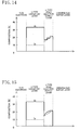
- FIG. 14 is a diagram for showing change of Al composition and In composition along line X-X′ of FIG. 1A ;
- FIG. 15 is a diagram for showing modification of the change of the Al composition and the In composition along line X-X′ of FIG. 1A .
- FIG. 1A is a cross-sectional view of the field effect transistor of Embodiment 1.
- an undoped GaN buffer layer 2 is formed on a sapphire substrate 1 by epitaxial growth.
- a two-dimensional electron gas 7 is generated in an upper portion of the undoped GaN buffer layer 2 , so that the upper portion of the undoped GaN buffer layer 2 can function as a channel layer of the field effect transistor.
- An n-type AlGaN electron supply layer 3 and an n-type InAlGaN cap layer 4 are successively formed on the undoped GaN buffer layer 2 by the epitaxial growth.
- a recess reaching the n-type AlGaN electron supply layer 3 is formed in a given portion of the n-type InAlGaN cap layer 4 , and a Pd—Si (i.e., an alloy of Pd and Si) Schottky electrode 6 working as a gate electrode is formed on the n-type AlGaN electron supply layer 3 exposed in the recess.
- Ti/Al (i.e., multilayered Ti and Al) ohmic electrodes 5 working as a source electrode and a drain electrode are formed on the n-type InAlGaN cap layer 4 on the respectively sides of the Schottky electrode 6 .
- the undoped GaN buffer layer 2 has a thickness of, for example, 2500 nm
- the n-type AlGaN electron supply layer 3 has a thickness of, for example, 25 nm
- the n-type InAlGaN cap layer 4 has a thickness of, for example, 50 nm.
- the impurity concentration in the n-type AlGaN electron supply layer 3 is, for example, approximately 4.0 ⁇ 10 18 atoms/cm 3
- the impurity concentration in the n-type InAlGaN cap layer 4 is, for example, approximately 1.0 ⁇ 10 19 atoms/cm 3 .
- FIG. 1B is a diagram for showing change of Al composition and In composition along line X-X′ of FIG. 1A
- FIG. 1C is a diagram for showing change of electron potential energy along line X-X′ of FIG. 1A .
- the Al composition in the n-type AlGaN electron supply layer 3 is changed along the thickness direction as a characteristic of this embodiment.
- the Al composition in the n-type AlGaN electron supply layer 3 is changed to be larger as a distance from the interface between the n-type AlGaN electron supply layer 3 and the n-type InAlGaN cap layer 4 is larger, so that the n-type AlGaN electron supply layer 3 and the n-type InAlGaN cap layer 4 can attain a substantially equal energy gap Eg on the interface therebetween, in other words, so that the lower ends of the conduction bands of these layers can be substantially continuous on the interface therebetween.
- the InAlGaN/AlGaN interface can be completely free from a potential barrier as shown in FIG. 1C .
- the n-type AlGaN electron supply layer 3 is made of AlGaN (with a thickness of 25 nm) in which the composition is changed from Al 0.15 Ga 0.85 N (with a band gap Eg of 3.68 eV) to Al 0.25 Ga 0.75 N (with a band gap Eg of 3.91 eV) along a direction from the n-type InAlGaN cap layer 4 toward the undoped GaN buffer layer 2 .
- the aforementioned effect can be attained.
- the n-type InAlGaN cap layer 4 is made of, for example, In 0.10 Al 0.47 Ga 0.43 N (with a band gap Eg of 3.81 eV and a thickness of 50 nm)
- the n-type AlGaN electron supply layer 3 is made of AlGaN (with a thickness of 25 nm) in which the composition is changed from Al 0.21 Ga 0.79 N (with a band gap Eg of 3.81 eV) to Al 0.25 Ga 0.75 N (with a band gap Eg of 3.91 eV) along the direction from the n-type InAlGaN cap layer 4 toward the undoped GaN buffer layer 2 .
- the aforementioned effect can be attained.
- the Al composition in the n-type AlGaN electron supply layer 3 is linearly increased (as gradient composition) as the distance from the interface with the n-type InAlGaN cap layer 4 is larger as shown in FIG. 1B .
- the Al composition may be increased in a stepwise manner (as stepwise composition) as the distance from the interface is larger, for example, as shown in FIG. 14 .
- the average Al composition in the n-type AlGaN electron supply layer 3 can be increased as compared with the case employing the gradient composition, and therefore, the concentration of generated carriers is increased, so as to reduce parasitic resistance.
- the influence of discontinuity of the conduction bands caused in employing the stepwise composition can be reduced by reducing discontinuity between respective steps.
- the n-type AlGaN electron supply layer 3 is made of AlGaN with stepwise composition (with a thickness of 25 nm in total) composed of a first layer of Al 0.18 Ga 0.82 N (with a band gap Eg of 3.75 eV and a thickness of 8 nm), a second layer of Al 0.22 Ga 0.78 N (with a band gap Eg of 3.83 eV and a thickness of 8 nm) and a third layer of Al 0.25 Ga 0.75 N (with a band gap Eg of 3.91 eV and a thickness of 9 nm).
- the n-type InAlGaN cap layer 4 is made of, for example, In 0.10 Al 0.47 Ga 0.43 N (with a band gap Eg of 3.81 eV and a thickness of 50 nm)
- the n-type AlGaN electron supply layer 3 is made of AlGaN with stepwise composition (with a thickness of 25 nm in total) composed of a first layer of Al 0.22 Ga 0.78 N (with a band gap Eg of 3.83 eV and a thickness of 5 mn), a second layer of Al 0.24 Ga 0.76 N (with a band gap Eg of 3.86 eV and a thickness of 5 nm) and a third layer of Al 0.25 Ga 0.75 N (with a band gap Eg of 3.91 eV and a thickness of 15 nm).
- the aforementioned effect can be attained. It is noted that the aforementioned values of the energy gaps of the InAlGaN are calculated with a bowing parameter set to 2.6 and that the aforementioned values of the energy gaps of the AlGaN are calculated with a bowing parameter set to 1.0.
- the Al composition in the n-type AlGaN electron supply layer 3 may be increased in the shape of a quadratic curve upward convex (as quadratic functional composition) as the distance from the interface with the n-type InAlGaN cap layer 4 is larger, for example, as shown in FIG. 15 .
- the average Al composition in the n-type AlGaN electron supply layer 3 can be increased as compared with the case employing the gradient composition, and therefore, the concentration of generated carriers is increased so as to reduce the parasitic resistance.
- the conduction bands are inclined in a direction for disturbing movement of electrons in the n-type AlGaN electron supply layer 3 , the discontinuity in the conduction bands caused in employing the stepwise composition can be avoided, and therefore, the influence derived from the discontinuity can be suppressed.
- the lattice constant of the electron supply layer (AlGaN layer) 3 and the lattice constant of the underlying buffer layer 2 are set to be equivalent.
- the Al composition and the In composition in the InAlGaN layer used as the cap layer 4 preferably satisfy the relationship of Formula 5.
- the energy gap of the InAlGaN layer can be freely changed in a region shown with a broken line in FIG. 2 .
- FIG. 2 shows the relationship between the energy gap and the lattice constant of a group III-V nitride compound semiconductor.
- the InAlGaN layer should have larger polarization than the AlGaN layer used as the electron supply layer 3 .
- the Al composition and the In composition in the InAlGaN layer are required to satisfy the following relationship: Polarization is provided as a sum of spontaneous polarization P sp peculiar to the material and piezoelectric polarization P pe caused through strain of the lattice caused by externally applied force or the like.
- the spontaneous polarization P sp and the piezoelectric polarization P pe are respectively represented by the following formulas 6 and 7 (see Journal Of Applied Physics, Vol. 87, pp.
- P sp In composition ⁇ P spInN +Al composition ⁇ P spAlN +Ga composition ⁇ P spGaN
- P pe e 33 ⁇ d z +e 31 ⁇ ( d x +d y )
- P spInN , P spAlN and P spGaN spontaneous polarization of InN, AlN and GaN, respectively
- e 3l and e 33 are piezoelectric coefficients
- d x and d y are strain of the lattice along the (0001) plane direction
- d z is strain of the lattice along a direction vertical to the (0001) plane.
- FIG. 3 The dependency on the In composition of the polarization caused in the InAlGaN layer obtained based on Formulas 6 and 7 is shown in FIG. 3 .
- the calculation is performed, in consideration of the lattice matching between InAlGaN and GaN, on the assumption that the Al composition is 4.66 times as large as the In composition in accordance with Formula 5.
- FIG. 3 also shows polarization caused in an AlGaN layer with the Al composition of 20% as an example of the AlGaN layer used as the electron supply layer 3 . As shown in FIG.
- the In composition is set to 8% or more and the Al composition is set to 37% or more, that is, 4.66 times as large as the In composition.
- FIG. 4 shows the current-voltage characteristics of the field effect transistor of this embodiment (shown with solid lines).
- the ordinate indicates a drain current per unit gate width and the abscissa indicates a drain voltage.
- FIG. 4 also shows the current-voltage characteristics of a conventional field effect transistor of FIG. 9A (shown with broken lines).
- the rise of the drain current is obviously more abrupt than in the conventional field effect transistor. This is because a potential barrier is not formed on the interface between the cap layer and the electron supply layer in this embodiment while it is formed in the conventional field effect transistor.
- the n-type InAlGaN cap layer 4 is stacked on the n-type AlGaN electron supply layer 3 in which the Al composition is changed along the thickness direction. Therefore, the lower ends of the conduction bands of the cap layer 4 and the electron supply layer 3 can be made substantially continuous on the hetero interface between these layers. Accordingly, a potential barrier can be lowered on the hetero interface between the cap layer 4 and the electron supply layer 3 , and hence, the increase of the parasitic resistance can be suppressed, so that the device characteristics such as the high-frequency characteristics can be largely improved.
- the ohmic electrodes 5 (working as the source electrode and the drain electrode) with very low resistance of 3 ⁇ 10 ⁇ 6 ⁇ cm 2 or less can be formed on the n-type InAlGaN cap layer 4 .
- FIG. 12 shows the relationship, obtained by the present inventors, between the work functions of metals and the Schottky barrier height ⁇ of AlGaN, GaN and InAlGaN.
- the height ⁇ is very small with respect to any metal. This reveals that InAlGaN has large electron affinity, and since the height ⁇ is small in using any metal, an ohmic electrode can be easily formed on n-type InAlGaN.
- FIG. 13 shows the current-voltage characteristics, obtained by the present inventors, of GaN and InAlGaN in using Mo (molybdenum) for a Schottky electrode.
- Mo molybdenum
- FIGS. 5A through 5D are cross-sectional views for showing procedures in the method for fabricating the field effect transistor of this embodiment.
- an undoped GaN buffer layer 2 , an n-type AlGaN electron supply layer 3 and an n-type InAlGaN cap layer 4 are successively formed on the (0001) plane of a sapphire substrate 1 by metal organic chemical vapor deposition (MOCVD).
- MOCVD metal organic chemical vapor deposition
- the n-type AlGaN electron supply layer 3 has a larger energy gap than the undoped GaN buffer layer 2 .
- the n-type AlGaN electron supply layer 3 and the n-type InAlGaN cap layer 4 are doped with Si by using a SiH 4 gas.
- the Al composition is changed along the thickness direction.
- the Al composition in the n-type AlGaN electron supply layer 3 is changed to be larger as a distance from the interface between the n-type AlGaN electron supply layer 3 and the n-type InAlGaN cap layer 4 is larger.
- the energy gap of the n-type AlGaN electron supply layer 3 and the energy gap of the n-type InAlGaN cap layer 4 are made substantially equivalent to each other on the InAlGaN/AlGaN hetero interface.
- a photoresist (not shown) having a stripe-shaped opening is formed on the n-type InAlGaN cap layer 4 .
- the width of the stripe is, for example, approximately 5 ⁇ m.
- the n-type InAlGaN cap layer 4 is selectively removed by induced coupled plasma (ICP) etching using, for example, a Cl 2 gas, so as to form a recess for exposing the n-type AlGaN electron supply layer 3 therein as shown in FIG. 5B .
- ICP induced coupled plasma
- Ti/Al ohmic electrodes 5 working as a source electrode and a drain electrode are formed on the respective sides of the recess on the n-type InAlGaN cap layer 4 by, for example, electron beam evaporation and lift-off.
- annealing is performed, for example, in a N 2 atmosphere at 600° C. for reducing contact resistance.
- the temperature for the annealing is preferably lower than the temperature at which the n-type InAlGaN cap layer 4 is formed.
- crystallinity degradation of the n-type InAlGaN cap layer 4 otherwise caused in the annealing can be suppressed so as to retain high crystallinity, and hence, the increase of the parasitic resistance can be suppressed.
- a Pd—Si (i.e., an alloy of Pd and Si) Schottky electrode 6 working as a gate electrode is formed on the n-type AlGaN electrons supply layer 3 exposed within the recess by, for example, the electron beam evaporation and the lift-off.
- the field effect transistor of this embodiment shown in FIG. 1A can be completed.
- the field effect transistor of this embodiment shown in FIG. 1A since the field effect transistor of this embodiment shown in FIG. 1A can be obtained, the potential barrier formed on the hetero interface between the cap layer 4 and the electron supply layer 3 can be lowered. As a result, the increase of the parasitic resistance can be suppressed, so as to largely improve the device characteristics such as the high-frequency characteristics.
- the impurity concentration is preferably higher in the uppermost portion of the n-type InAlGaN cap layer 4 than in other portions. Also, after adding the impurity, annealing is performed preferably at a temperature lower than the temperature at which the n-type InAlGaN cap layer 4 is formed.
- the impurity concentration in the n-type InAlGaN cap layer 4 can be increased, and therefore, contact resistance between the Ti/Al ohmic electrodes 5 and the n-type InAlGaN cap layer 4 can be reduced and the resistance of the n-type InAlGaN cap layer 4 can be reduced. Furthermore, the crystallinity degradation of the n-type InAlGaN cap layer 4 otherwise caused in the annealing can be suppressed so as to retain high crystallinity, and therefore, the parasitic resistance can be reduced.
- FIGS. 6A through 6F are cross-sectional views for showing procedures in the method for fabricating the field effect transistor of this modification.
- the recess corresponding to a gate electrode forming region is formed by etching the n-type InAlGaN cap layer 4 in the procedure shown in FIG. 5B in Embodiment 1, the recess is formed by regrowing the n-type InAlGaN cap layer 4 after masking a gate electrode forming region on the n-type AlGaN electron supply layer 3 as described below in this modification.
- an undoped GaN buffer layer 2 and an n-type AlGaN electron supply layer 3 are successively formed on the (0001) plane of a sapphire substrate 1 by the MOCVD. It is noted that the energy gap of the n-type AlGaN electron supply layer 3 is larger than the energy gap of the undoped GaN buffer layer 2 . Also, the n-type AlGaN electron supply layer 3 is doped with Si by using a SiH 4 gas. Furthermore, in forming the n-type AlGaN electron supply layer 3 , the Al composition is changed along the thickness direction.
- the Al composition in the n-type AlGaN electron supply layer 3 is changed to be larger as a distance from the interface between the n-type AlGaN electron supply layer 3 and an n-type InAlGaN cap layer 4 (see FIG. 6C ) is larger.
- the energy gap of the n-type AlGaN electron supply layer 3 and the energy gap of the n-type InAlGaN cap layer 4 are made substantially equivalent to each other on the InAlGaN/AlGaN hetero interface.
- the lower ends of the conduction bands of the n-type AlGaN electron supply layer 3 and the n-type InAlGaN cap layer 4 are made substantially continuous on the InAlGaN/AlGaN hetero interface.
- a SiO 2 film with a thickness of approximately 100 nm is formed on the n-type AlGaN electron supply layer 3 by vapor phase deposition using, for example, a SiH 4 gas and an O 2 gas, such as CVD (chemical vapor deposition).
- CVD chemical vapor deposition
- the SiO 2 film is selectively etched with a hydrofluoric acid (HF) aqueous solution by using, for example, a photoresist as a mask.
- a SiO 2 mask 8 is formed as shown in FIG. 6B .
- the thickness of the SiO 2 film used as the SiO 2 mask 8 is preferably larger than the thickness of the n-type InAlGaN cap layer 4 subsequently formed.
- the n-type InAlGaN cap layer 4 can be prevented from being formed on the SiO 2 mask 8 , and hence, the dimension of a recess formed by removing the SiO 2 mask 8 in a subsequent procedure can be accurately controlled. Accordingly, a fine gate electrode can be formed, and hence, the channel length can be reduced, so that parasitic resistance derived from channel resistance can be reduced.
- an InAlGaN layer is started to grow by, for example, the MOCVD from a portion of the n-type AlGaN electron supply layer 3 not covered with the SiO 2 mask 8 , thereby forming the n-type InAlGaN cap layer 4 .
- the thickness of the n-type InAlGaN cap layer 4 is smaller than the thickness of the n-type AlGaN electron supply layer 3 .
- the SiO 2 mask 8 is removed by using, for example, a hydrofluoric acid (HF) aqueous solution, thereby forming a recess reaching the n-type AlGaN electron supply layer 3 .
- HF hydrofluoric acid
- Ti/Al ohmic electrodes 5 working as a source electrode and a drain electrode are formed on the respective sides of the recess on the n-type InAlGaN cap layer 4 by, for example, the electron beam evaporation and the lift-off as shown in FIG. 6E .
- annealing is performed, for example, in a N 2 atmosphere at 600° C. for reducing contact resistance.
- the temperature for the annealing is preferably lower than the temperature at which the n-type InAlGaN cap layer 4 is formed.
- the crystallinity degradation of the n-type InAlGaN cap layer 4 otherwise caused in the annealing can be suppressed so as to retain high crystallinity, and hence, the increase of the parasitic resistance can be suppressed.
- a Pd—Si (i.e., an alloy of Pd and Si) Schottky electrode 6 working as a gate electrode is formed on the n-type AlGaN electron supply layer 3 within the recess by, for example, the electron beam evaporation and the lift-off as shown in FIG. 6F .
- the field effect transistor of Embodiment 1 shown in FIG. 1A can be completed.
- the same effects as those of Embodiment 1 can be attained. Also, since the recess for forming the gate electrode can be formed without damaging a region below the gate electrode working as a channel region by etching, degradation of the transistor characteristics such as the increase of the parasitic resistance derived from the channel resistance can be prevented.
- SiO 2 is used as a material for the mask 8 in this modification, another material with a selection ratio against a group III-V nitride compound semiconductor may be used instead.
- FIG. 7 is a cross-sectional view of the field effect transistor of this embodiment.
- like reference numerals are used to refer to like elements used in Embodiment 1 shown in FIG. 1A .
- Embodiment 2 is different from Embodiment 1 in the following points as described below: Directly below an n-type InAlGaN cap layer 4 , a multilayered film including at least one cycle of another InAlGaN layer and an AlGaN layer alternately stacked is provided; and an n-type AlGaN electron supply layer 3 (in which the Al composition is changed along the thickness direction as in Embodiment 1) is provided with a delta dope layer (i.e., a region including an impurity for providing the conductivity type to the n-type AlGaN electron supply layer 3 so as to cause a pulse-shaped profile along a direction vertical to the interface between the n-type AlGaN electron supply layer 3 and the n-type InAlGaN cap layer 4 ).
- an AlN spacer layer 11 and an n-type AlGaN electron supply layer 3 are formed by the epitaxial growth on an undoped GaN buffer layer 2 formed on a sapphire substrate 1 .
- a two-dimensional electron gas 7 is generated in an upper portion of the undoped GaN buffer layer 2 , so that the upper portion of the undoped GaN buffer layer 2 can function as a channel layer of the field effect transistor.
- a SiO 2 mask 20 is provided in a lower portion of the undoped GaN buffer layer 2 .
- An n-type InAlGaN cap layer 4 is formed by the epitaxial growth on the multilayered film 10 .
- a recess reaching the n-type AlGaN electron supply layer 3 is formed in a given portion of the n-type InAlGaN cap layer 4 , and a Pd—Si (i.e., an alloy of Pd and Si) Schottky electrode 6 working as a gate electrode is formed on the n-type AlGaN electron supply layer 3 exposed within the recess.
- Ti/Al (i.e., multilayered Ti and Al) ohmic electrodes 5 working as a source electrode and a drain electrode are formed on the respective sides of the Schottky electrode 6 on the n-type InAlGaN cap layer 4 .
- the Al composition in the n-type AlGaN electron supply layer 3 is changed along the thickness direction. Specifically, the Al composition in the n-type AlGaN electron supply layer 3 is changed to be larger as a distance from the interface between the n-type AlGaN electron supply layer 3 and the n-type InAlGaN cap layer 4 is larger, so that the n-type AlGaN electron supply layer 3 and the n-type InAlGaN cap layer 4 can attain a substantially equal energy gap Eg on the interface therebetween (in which the multilayered film 10 is provided in this embodiment), in other words, so that the lower ends of the conduction bands of these layers can be substantially continuous on the interface (see FIG. 1B ).
- the InAlGaN/AlGaN interface can be completely free from a potential barrier (see FIG. 1C ).
- a delta dope layer 9 is formed in the vicinity of the multilayered film 10 in the n-type AlGaN electron supply layer 3 .
- the impurity concentration in the delta dope layer 9 is approximately 1 ⁇ 10 19 atoms/cm 3 or more.
- the undoped GaN buffer layer 2 has a thickness of, for example, 2500 nm
- the AlN spacer layer 11 has a thickness of, for example, 1 nm
- the n-type AlGaN electron supply layer 3 has a thickness of, for example, 25 nm
- the delta dope layer 9 has a thickness of, for example, 5 nm or less
- the multilayered film 10 has a thickness of, for example, 21 nm
- the n-type InAlGaN cap layer 4 has a thickness of, for example, 50 nm.
- the impurity concentration in the n-type AlGaN electron supply layer 3 is, for example, approximately 4.0 ⁇ 10 18 atoms/cm 3
- the impurity concentration in the delta dope layer 9 is, for example, 1 ⁇ 10 19 atoms/cm 3 or more
- the impurity concentration in the multilayered film 10 as a whole is, for example, approximately 1.0 ⁇ 10 19 atoms/cm 3
- the impurity concentration in the n-type InAlGaN cap layer 4 is, for example, approximately 1.0 ⁇ 10 19 atoms/cm 3 .
- the Al composition in the n-type AlGaN electron supply layer 3 is changed so that the energy gaps Eg of the n-type AlGaN electron supply layer 3 and the n-type InAlGaN cap layer 4 can be substantially equal to each other on the interface between these layers (in which the multilayered film 10 is provided in this embodiment), in other words, so that the lower ends of the conduction bands of these layers can be substantially continuous on the interface. Therefore, a potential barrier formed on the hetero interface between the cap layer 4 and the electron supply layer 3 can be lowered, and hence, the increase of the parasitic resistance can be suppressed, so that the device characteristics such as the high-frequency characteristics can be largely improved.
- the delta dope layer 9 is provided in the n-type AlGaN electron supply layer 3 . Since the thus added impurity lowers the conduction band of the n-type AlGaN electron supply layer 3 , electrons can easily pass through the potential barrier. In other words, the influence of the potential barrier can be cancelled, so as to further suppress the increase of the parasitic resistance.
- the multilayered film 10 including at least one cycle of the InAlGaN layer and the AlGaN layer alternately stacked is provided between the n-type AlGaN electron supply layer 3 and the n-type InAlGaN cap layer 4 .
- the influence of the potential barrier formed between the n-type AlGaN electron supply layer 3 and the n-type InAlGaN cap layer 4 can be suppressed, so as to suppress the increase of the parasitic resistance derived from the potential barrier, and at the same time, parasitic resistance along a horizontal direction (i.e., a direction parallel to the interface between the n-type AlGaN electron supply layer 3 and the n-type InAlGaN cap layer 4 ) can be largely reduced.
- the AlN spacer layer 11 is provided between the undoped GaN buffer layer 2 and the n-type AlGaN electron supply layer 3 , scattering of alloy can be suppressed, so as to improve the mobility of electrons in the channel, and therefore, the parasitic resistance derived from channel resistance can be reduced.
- the field effect transistor of this embodiment includes the n-type InAlGaN cap layer 4 directly under which the multilayered film 10 including at least one cycle of the InAlGaN layer and the AlGaN layer alternately stacked is formed and the n-type AlGaN electron supply layer 3 in which the delta dope layer is provided and the Al composition is changed along the thickness direction. Therefore, the increase of the parasitic resistance on the hetero interface between the cap layer 4 and the electron supply layer 3 can be suppressed, so as to largely improve the device characteristics such as the high-frequency characteristics.
- FIGS. 8A through 8F are cross-sectional views for showing procedures in the method for fabricating the field effect transistor of this embodiment.
- an undoped GaN buffer layer 2 is grown halfway on the (0001) plane of a sapphire substrate 1 by the MOCVD. Subsequently, a SiO 2 film with a thickness of approximately 100 nm is formed on the undoped GaN buffer layer 2 by the vapor phase deposition using, for example, a SiH 4 gas and an O 2 gas (such as the CVD).
- the SiO 2 film is selectively etched with a hydrofluoric acid (HF) aqueous solution by using, for example, a photoresist as a mask, so as to form a plurality of SiO 2 stripes with a width of 10 ⁇ m by forming a plurality of stripe-shaped openings each with a width of, for example, 5 ⁇ m in the SiO 2 film.
- a SiO 2 mask 20 is formed.
- GaN is regrown from the surface of a portion of the undoped GaN buffer layer 2 not covered with the SiO 2 mask 20 by, for example, the MOCVD, thereby completing the undoped GaN buffer layer 2 with a desired thickness.
- the MOCVD the crystal of the GaN is grown on the SiO 2 mask 20 in the lateral direction, and hence, the threading dislocation density is largely reduced on the SiO 2 mask 20 , resulting in attaining a dislocation density of the order of 10 6 cm ⁇ 2 .
- an AlN spacer layer 11 and an n-type AlGaN electron supply layer 3 are successively formed on the undoped GaN buffer layer 2 by, for example, the MOCVD. It is noted that the energy gap of the n-type AlGaN electron supply layer 3 is larger than that of the undoped GaN buffer layer 2 . Also, the n-type AlGaN electron supply layer 3 is doped with Si by using a SiH 4 gas.
- the Al composition is changed along the thickness direction. Specifically, the Al composition in the n-type AlGaN electron supply layer 3 is changed to be larger as a distance from the interface between the n-type AlGaN electron supply layer 3 and an n-type InAlGaN cap layer 4 described below is larger.
- the energy gap of the n-type AlGaN electron supply layer 3 and the energy gap of the n-type InAlGaN cap layer 4 are set to be substantially equivalent to each other on the InAlGaN/AlGaN hetero interface.
- a multilayered film 10 including at least one cycle of an n-type InAlGaN thin film with a thickness of, for example, 1.5 nm and an n-type AlGaN thin film with a thickness of, for example, 1.5 nm alternately stacked is formed on the n-type AlGaN electron supply layer 3 by the epitaxial growth, and the n-type InAlGaN cap layer 4 is formed on the multilayered film 10 .
- the n-type InAlGaN cap layer 4 is doped with Si by using a SiH 4 gas.
- a photoresist (not shown) having a stripe-shaped opening is formed on the n-type InAlGaN cap layer 4 .
- the width of the stripe is, for example, approximately 5 ⁇ m.
- the n-type InAlGaN cap layer 4 is selectively removed as shown in FIG. 8D by the ICP etching using, for example, a Cl 2 gas, thereby forming a recess for exposing the n-type AlGaN electron supply layer 3 therein.
- the recess is formed so that a portion of the n-type AlGaN electron supply layer 3 deeper than the delta dope layer 9 can be exposed.
- Ti/Al ohmic electrodes 5 working as a source electrode and a drain electrode are formed on the n-type InAlGaN cap layer 4 on the respective sides of the recess by, for example, the electron beam evaporation and the lift-off.
- annealing is performed, for example, in a N 2 atmosphere at 600° C. for reducing contact resistance.
- the temperature for the annealing is preferably lower than a temperature at which the n-type InAlGaN cap layer 4 is formed.
- the crystallinity degradation of the n-type InAlGaN cap layer 4 otherwise caused in the annealing can be suppressed so as to retain high crystallinity, and hence, the increase of the parasitic resistance can be suppressed.
- a Pd—Si (i.e., an alloy of Pd and Si) Schottky electrode 6 working as a gate electrode is formed on the n-type AlGaN electron supply layer 3 exposed within the recess by, for example, the electron beam evaporation and the lift-off.
- the field effect transistor of this embodiment shown in FIG. 7 can be completed.
- the field effect transistor of this embodiment shown in FIG. 7 can be obtained. Therefore, a potential barrier formed on the hetero interface between the cap layer 4 and the electron supply layer 3 can be lowered, so as to suppress the increase of the parasitic resistance, resulting in largely improving the device characteristics such as the high-frequency characteristics.
- the impurity concentration in the uppermost portion of the n-type InAlGaN cap layer 4 is preferably higher than in other portions.
- annealing is performed preferably at a temperature lower than the temperature at which the n-type InAlGaN cap layer 4 is formed.
- the impurity concentration in the n-type InAlGaN cap layer 4 can be increased, and therefore, the contact resistance between the Ti/Al ohmic electrodes 5 and the n-type InAlGaN cap layer 4 can be reduced and the resistance of the n-type InAlGaN cap layer 4 can be reduced. Furthermore, the crystallinity degradation of the n-type InAlGaN cap layer 4 otherwise caused in the annealing can be suppressed, so as to retain high crystallinity, and hence, the parasitic resistance can be reduced.
- the multilayered film including at least one cycle of an InAlGaN layer and an AlGaN layer alternately stacked is used as the multilayered film 10 in this embodiment, the same effects can be attained even when a multilayered film includes at least one cycle of a GaN layer and an AlGaN layer alternately stacked.
- the crystals of the undoped GaN buffer layer 2 , the n-type AlGaN electron supply layer 3 and the like are grown on the (0001) plane of the sapphire substrate 1 in each of Embodiments 1 and 2, the plane direction of the crystal growth face is not particularly specified.
- a plane direction with an off angle against a typical plane such as the (0001 plane may be employed.
- the sapphire substrate 1 is used in each of Embodiments 1 and 2, even when a substrate of SiC, GaN, AlN, Si, GaAs, ZnO, MgO, ZrB 2 , LiGaO 2 , LiAlO 2 , GaP, InP or mixed crystal of at least two of them is used, a nitride semiconductor with high crystallinity can be epitaxially grown as in these embodiments.
- the epitaxially grown layers (such as the GaN buffer layer 2 and the n-type AlGaN electron supply layer 3 ) included in the field effect transistor may have any composition ratio or any multilayered structure as far as desired device characteristics can be realized.
- the crystal growth method for the epitaxially grown layers is not limited to the MOCVD but may be, for example, molecular beam epitaxy (MBE) or hydride vapor phase epitaxy (HVPE).
- the respective epitaxially grown layers may be formed by different crystal growth methods.
- the epitaxially grown layers may include, as a composing element, a group V element such as As or P or a group III element such as B.
- each epitaxially grown layer is not limited to the GaN-based semiconductor layer but may be a GaAs-based semiconductor layer or an InP-based semiconductor layer.
- GaN and AlGaN are respectively used as the buffer layer 2 and the electron supply layer 3 in each of Embodiments 1 and 2, a combination of GaN and AlN, a combination of InAlGaN and AlN or a combination of InGaN and GaN may be used instead.
Landscapes
- Engineering & Computer Science (AREA)
- Microelectronics & Electronic Packaging (AREA)
- Power Engineering (AREA)
- Physics & Mathematics (AREA)
- Ceramic Engineering (AREA)
- Condensed Matter Physics & Semiconductors (AREA)
- General Physics & Mathematics (AREA)
- Computer Hardware Design (AREA)
- Junction Field-Effect Transistors (AREA)
Abstract
Description
f T =g m/(2πL g) Formula 1:
wherein Lg is a gate length. As is obvious from Formula 1, it is significant to increase the mutual conductance gm for improving the cut-off frequency fT. In consideration of parasitic resistance, the mutual conductance gm is represented by the following formula 2:
g m =g mint/(1+R s ·g mint) Formula 2:
wherein gmint is intrinsic mutual conductance determined depending upon the material and the structure and Rs is parasitic resistance from an ohmic electrode to a channel and is designated as source resistance. As is understood from Formula 2, the mutual conductance gm increases as the source resistance Rs reduces, and as a result, the cut-off frequency fT also increases. Accordingly, in order to improve the high-frequency characteristics of the HFET, it is necessary to reduce the parasitic resistance.
Eg InAlGaN=In composition×Eg InN+Al composition×Eg AlN+Ga composition×Eg GaN−C×(In composition+Al composition)×Ga composition Formula 3:
wherein EgInN, EgAlN and EgGaN are energy gaps of InN, AlN and GaN, respectively, and C is a bowing parameter. Although the bowing parameter of InAlGaN is conventionally regarded as approximately 1 eV as described above, the bowing parameter obtained from the result shown in
a InAlGaN=In composition×a InN+Al composition×a AlN+Ga composition×a GaN Formula 4:
wherein aInNl , aAlN and aGaN are lattice constants of InN, AlN and GaN, respectively. On the basis of a condition for making the lattice constant aInAlGaN of the InAlGaN equal to the lattice constant of the GaN, the following
Al composition=4.66×In composition Formula 5:
P sp=In composition×P spInN+Al composition×P spAlN+Ga composition×P spGaN Formula 6:
P pe =e 33 ·d z +e 31·(d x +d y) Formula 7:
wherein PspInN, PspAlN and PspGaN are spontaneous polarization of InN, AlN and GaN, respectively, e3l and e33 are piezoelectric coefficients, dx and dy are strain of the lattice along the (0001) plane direction, and dz is strain of the lattice along a direction vertical to the (0001) plane. The dependency on the In composition of the polarization caused in the InAlGaN layer obtained based on
Claims (12)
Applications Claiming Priority (2)
| Application Number | Priority Date | Filing Date | Title |
|---|---|---|---|
| JP2005041336 | 2005-02-17 | ||
| JP2005-041336 | 2005-02-17 |
Publications (2)
| Publication Number | Publication Date |
|---|---|
| US20060180831A1 US20060180831A1 (en) | 2006-08-17 |
| US7714359B2 true US7714359B2 (en) | 2010-05-11 |
Family
ID=36814787
Family Applications (1)
| Application Number | Title | Priority Date | Filing Date |
|---|---|---|---|
| US11/355,939 Active 2028-10-17 US7714359B2 (en) | 2005-02-17 | 2006-02-17 | Field effect transistor having nitride semiconductor layer |
Country Status (1)
| Country | Link |
|---|---|
| US (1) | US7714359B2 (en) |
Cited By (3)
| Publication number | Priority date | Publication date | Assignee | Title |
|---|---|---|---|---|
| US20110180854A1 (en) * | 2010-01-27 | 2011-07-28 | National Semiconductor Corporation | Normally-off gallium nitride-based semiconductor devices |
| US20120187413A1 (en) * | 2011-01-26 | 2012-07-26 | Kabushiki Kaisha Toshiba | Nitride semiconductor device and method for manufacturing same |
| US10211323B2 (en) | 2015-09-30 | 2019-02-19 | Sumitomo Electric Industries, Ltd. | Hemt having heavily doped N-type regions and process of forming the same |
Families Citing this family (29)
| Publication number | Priority date | Publication date | Assignee | Title |
|---|---|---|---|---|
| WO2007091383A1 (en) * | 2006-02-10 | 2007-08-16 | Nec Corporation | Semiconductor device |
| KR100756841B1 (en) * | 2006-03-13 | 2007-09-07 | 서울옵토디바이스주식회사 | Light emitting diode having graded buffer layer and fabrication method thereof |
| JP5179023B2 (en) * | 2006-05-31 | 2013-04-10 | パナソニック株式会社 | Field effect transistor |
| US7737476B2 (en) * | 2007-02-15 | 2010-06-15 | Cree, Inc. | Metal-semiconductor field effect transistors (MESFETs) having self-aligned structures |
| US20090199887A1 (en) * | 2008-02-08 | 2009-08-13 | North Carolina State University And Nextreme Thermal Solutions, Inc. | Methods of forming thermoelectric devices including epitaxial thermoelectric elements of different conductivity types on a same substrate and related structures |
| JP4761319B2 (en) * | 2008-02-19 | 2011-08-31 | シャープ株式会社 | Nitride semiconductor device and power conversion device including the same |
| JP2010225765A (en) | 2009-03-23 | 2010-10-07 | Panasonic Corp | Semiconductor device and method of manufacturing the same |
| US8384129B2 (en) * | 2009-06-25 | 2013-02-26 | The United States Of America, As Represented By The Secretary Of The Navy | Transistor with enhanced channel charge inducing material layer and threshold voltage control |
| US20110057198A1 (en) * | 2009-08-28 | 2011-03-10 | The Regents Of The University Of California | TECHNIQUE FOR DEVELOPMENT OF HIGH CURRENT DENSITY HETEROJUNCTION FIELD EFFECT TRANSISTORS BASED ON (10-10)-PLANE GaN BY DELTA-DOPING |
| US8338860B2 (en) * | 2009-10-30 | 2012-12-25 | Alpha And Omega Semiconductor Incorporated | Normally off gallium nitride field effect transistors (FET) |
| JP5866773B2 (en) * | 2011-02-25 | 2016-02-17 | 富士通株式会社 | Compound semiconductor device and manufacturing method thereof |
| JP5692357B2 (en) * | 2011-03-18 | 2015-04-01 | 富士通株式会社 | Compound semiconductor device and manufacturing method thereof |
| JP5895666B2 (en) * | 2012-03-30 | 2016-03-30 | 富士通株式会社 | Compound semiconductor device and manufacturing method thereof |
| CN103367417A (en) * | 2012-03-31 | 2013-10-23 | 稳懋半导体股份有限公司 | Group III nitride high electron mobility transistor (HEMT) |
| JP2013235873A (en) * | 2012-05-02 | 2013-11-21 | Renesas Electronics Corp | Semiconductor device and method of manufacturing the same |
| JP2014053418A (en) * | 2012-09-06 | 2014-03-20 | Fujitsu Ltd | Semiconductor device |
| US8896101B2 (en) * | 2012-12-21 | 2014-11-25 | Intel Corporation | Nonplanar III-N transistors with compositionally graded semiconductor channels |
| US9490357B2 (en) | 2013-07-15 | 2016-11-08 | Hrl Laboratories, Llc | Vertical III-nitride semiconductor device with a vertically formed two dimensional electron gas |
| CN103606560B (en) * | 2013-10-22 | 2016-07-06 | 石以瑄 | Reduce the impact of microcrack, and be used in the high charge mobility transistor of microwave integrated circuit and switched circuit |
| KR20150051822A (en) * | 2013-11-05 | 2015-05-13 | 삼성전자주식회사 | High electron mobility transistor and method of manufacturing the same |
| CN103824854B (en) * | 2014-02-22 | 2016-09-28 | 石以瑄 | Switched circuit based on HEMT and microwave integrated circuit |
| TWI577046B (en) * | 2014-12-23 | 2017-04-01 | 錼創科技股份有限公司 | Semiconductor light-emitting device and manufacturing method thereof |
| US9601610B1 (en) | 2015-06-18 | 2017-03-21 | Hrl Laboratories, Llc | Vertical super junction III/nitride HEMT with vertically formed two dimensional electron gas |
| JP6597046B2 (en) | 2015-08-20 | 2019-10-30 | 住友電気工業株式会社 | High electron mobility transistor |
| JP6690320B2 (en) | 2016-03-11 | 2020-04-28 | 住友電気工業株式会社 | High electron mobility transistor and method of manufacturing high electron mobility transistor |
| JP6870304B2 (en) * | 2016-12-05 | 2021-05-12 | 住友電気工業株式会社 | Manufacturing method of semiconductor devices |
| US11056434B2 (en) | 2017-01-26 | 2021-07-06 | Epistar Corporation | Semiconductor device having specified p-type dopant concentration profile |
| US10971652B2 (en) * | 2017-01-26 | 2021-04-06 | Epistar Corporation | Semiconductor device comprising electron blocking layers |
| CN113113476A (en) * | 2021-03-01 | 2021-07-13 | 西安电子科技大学 | GaN HEMT device suitable for low-working-voltage high-efficiency application and preparation method thereof |
Citations (2)
| Publication number | Priority date | Publication date | Assignee | Title |
|---|---|---|---|---|
| JP2002289837A (en) | 2001-03-27 | 2002-10-04 | Matsushita Electric Ind Co Ltd | Semiconductor device |
| JP2004022563A (en) | 2002-06-12 | 2004-01-22 | Sony Corp | METHOD FOR FORMING GaInN LAYER |
-
2006
- 2006-02-17 US US11/355,939 patent/US7714359B2/en active Active
Patent Citations (2)
| Publication number | Priority date | Publication date | Assignee | Title |
|---|---|---|---|---|
| JP2002289837A (en) | 2001-03-27 | 2002-10-04 | Matsushita Electric Ind Co Ltd | Semiconductor device |
| JP2004022563A (en) | 2002-06-12 | 2004-01-22 | Sony Corp | METHOD FOR FORMING GaInN LAYER |
Non-Patent Citations (2)
| Title |
|---|
| O. Amabacher, et al., "Two dimensional electron gases induced by spontaneous and piezoelectric polarization in undoped and doped AIGaN/GaN heterstructures," Journal of Applied Physics, Jan. 1, 2000, pp. 334-344, vol. 87, No. 1, American Institute of Physics. |
| T. Egawa, et al., "Recessed gate AIGaN/GaN modulation-doped field-effect transistors on sapphire," Applied Physics Letters, Jan. 3, 2000, pp. 121-123, vol. 76, No. 1, American Institute of Physics. |
Cited By (4)
| Publication number | Priority date | Publication date | Assignee | Title |
|---|---|---|---|---|
| US20110180854A1 (en) * | 2010-01-27 | 2011-07-28 | National Semiconductor Corporation | Normally-off gallium nitride-based semiconductor devices |
| US20120187413A1 (en) * | 2011-01-26 | 2012-07-26 | Kabushiki Kaisha Toshiba | Nitride semiconductor device and method for manufacturing same |
| US8759878B2 (en) * | 2011-01-26 | 2014-06-24 | Kabushiki Kaisha Toshiba | Nitride semiconductor device and method for manufacturing same |
| US10211323B2 (en) | 2015-09-30 | 2019-02-19 | Sumitomo Electric Industries, Ltd. | Hemt having heavily doped N-type regions and process of forming the same |
Also Published As
| Publication number | Publication date |
|---|---|
| US20060180831A1 (en) | 2006-08-17 |
Similar Documents
| Publication | Publication Date | Title |
|---|---|---|
| US7714359B2 (en) | Field effect transistor having nitride semiconductor layer | |
| US7705371B2 (en) | Field effect transistor having reduced contact resistance and method for fabricating the same | |
| US10566450B2 (en) | Normally-off HEMT transistor with selective generation of 2DEG channel, and manufacturing method thereof | |
| JP5208463B2 (en) | Nitride semiconductor device and method for manufacturing nitride semiconductor device | |
| US8198652B2 (en) | Field effect transistor with reduced gate leakage current | |
| JP2006261642A (en) | Field effect transistor and method of fabricating the same | |
| JP5810293B2 (en) | Nitride semiconductor device | |
| JP5190923B2 (en) | Nitride semiconductor transistor having GaN as channel layer and manufacturing method thereof | |
| WO2012014352A1 (en) | Field effect transistor | |
| US8344422B2 (en) | Semiconductor device | |
| US7985984B2 (en) | III-nitride semiconductor field effect transistor | |
| KR101365302B1 (en) | Compound semiconductor device and method for fabricating the same | |
| US20110272740A1 (en) | Field effect transistor and method of manufacturing the same | |
| US20120299060A1 (en) | Nitride semiconductor device and manufacturing method thereof | |
| US20100230687A1 (en) | Iii nitride electronic device and iii nitride semiconductor epitaxial substrate | |
| JP2007088185A (en) | Semiconductor device and its fabrication process | |
| US20110215424A1 (en) | Semiconductor device and manufacturing method thereof | |
| US20220093779A1 (en) | Gallium nitride enhancement mode device | |
| CN115188808A (en) | Doped barrier layers in epitaxial group III nitrides | |
| US8089096B2 (en) | Field effect transistor with main surface including C-axis | |
| US20220157980A1 (en) | Nitride semiconductor device | |
| US8283700B2 (en) | Field effect transistor and manufacturing method thereof | |
| JP2023116995A (en) | Nitride semiconductor device and manufacturing method for nitride semiconductor device | |
| KR101670238B1 (en) | Manufacturing method for semiconductor device | |
| US11699723B1 (en) | N-polar III-nitride device structures with a p-type layer |
Legal Events
| Date | Code | Title | Description |
|---|---|---|---|
| AS | Assignment |
Owner name: MATSUSHITA ELECTRIC INDUSTRIAL CO., LTD.,JAPAN Free format text: ASSIGNMENT OF ASSIGNORS INTEREST;ASSIGNORS:NAKAZAWA, SATOSHI;UEDA, TETSUZO;TANAKA, TSUYOSHI;REEL/FRAME:017798/0394 Effective date: 20060130 Owner name: MATSUSHITA ELECTRIC INDUSTRIAL CO., LTD., JAPAN Free format text: ASSIGNMENT OF ASSIGNORS INTEREST;ASSIGNORS:NAKAZAWA, SATOSHI;UEDA, TETSUZO;TANAKA, TSUYOSHI;REEL/FRAME:017798/0394 Effective date: 20060130 |
|
| AS | Assignment |
Owner name: PANASONIC CORPORATION, JAPAN Free format text: CHANGE OF NAME;ASSIGNOR:MATSUSHITA ELECTRIC INDUSTRIAL CO., LTD.;REEL/FRAME:021897/0671 Effective date: 20081001 Owner name: PANASONIC CORPORATION,JAPAN Free format text: CHANGE OF NAME;ASSIGNOR:MATSUSHITA ELECTRIC INDUSTRIAL CO., LTD.;REEL/FRAME:021897/0671 Effective date: 20081001 |
|
| STCF | Information on status: patent grant |
Free format text: PATENTED CASE |
|
| FEPP | Fee payment procedure |
Free format text: PAYOR NUMBER ASSIGNED (ORIGINAL EVENT CODE: ASPN); ENTITY STATUS OF PATENT OWNER: LARGE ENTITY |
|
| FPAY | Fee payment |
Year of fee payment: 4 |
|
| MAFP | Maintenance fee payment |
Free format text: PAYMENT OF MAINTENANCE FEE, 8TH YEAR, LARGE ENTITY (ORIGINAL EVENT CODE: M1552) Year of fee payment: 8 |
|
| MAFP | Maintenance fee payment |
Free format text: PAYMENT OF MAINTENANCE FEE, 12TH YEAR, LARGE ENTITY (ORIGINAL EVENT CODE: M1553); ENTITY STATUS OF PATENT OWNER: LARGE ENTITY Year of fee payment: 12 |