US10629568B2 - Stacked integrated circuits with redistribution lines - Google Patents
Stacked integrated circuits with redistribution lines Download PDFInfo
- Publication number
- US10629568B2 US10629568B2 US16/390,894 US201916390894A US10629568B2 US 10629568 B2 US10629568 B2 US 10629568B2 US 201916390894 A US201916390894 A US 201916390894A US 10629568 B2 US10629568 B2 US 10629568B2
- Authority
- US
- United States
- Prior art keywords
- substrate
- dielectric layers
- top surface
- metal pad
- integrated circuit
- Prior art date
- Legal status (The legal status is an assumption and is not a legal conclusion. Google has not performed a legal analysis and makes no representation as to the accuracy of the status listed.)
- Active
Links
Images


Classifications
-
- H—ELECTRICITY
- H01—ELECTRIC ELEMENTS
- H01L—SEMICONDUCTOR DEVICES NOT COVERED BY CLASS H10
- H01L25/00—Assemblies consisting of a plurality of individual semiconductor or other solid state devices ; Multistep manufacturing processes thereof
- H01L25/03—Assemblies consisting of a plurality of individual semiconductor or other solid state devices ; Multistep manufacturing processes thereof all the devices being of a type provided for in the same subgroup of groups H01L27/00 - H01L33/00, or in a single subclass of H10K, H10N, e.g. assemblies of rectifier diodes
- H01L25/04—Assemblies consisting of a plurality of individual semiconductor or other solid state devices ; Multistep manufacturing processes thereof all the devices being of a type provided for in the same subgroup of groups H01L27/00 - H01L33/00, or in a single subclass of H10K, H10N, e.g. assemblies of rectifier diodes the devices not having separate containers
- H01L25/065—Assemblies consisting of a plurality of individual semiconductor or other solid state devices ; Multistep manufacturing processes thereof all the devices being of a type provided for in the same subgroup of groups H01L27/00 - H01L33/00, or in a single subclass of H10K, H10N, e.g. assemblies of rectifier diodes the devices not having separate containers the devices being of a type provided for in group H01L27/00
- H01L25/0657—Stacked arrangements of devices
-
- H—ELECTRICITY
- H01—ELECTRIC ELEMENTS
- H01L—SEMICONDUCTOR DEVICES NOT COVERED BY CLASS H10
- H01L21/00—Processes or apparatus adapted for the manufacture or treatment of semiconductor or solid state devices or of parts thereof
- H01L21/70—Manufacture or treatment of devices consisting of a plurality of solid state components formed in or on a common substrate or of parts thereof; Manufacture of integrated circuit devices or of parts thereof
- H01L21/71—Manufacture of specific parts of devices defined in group H01L21/70
- H01L21/768—Applying interconnections to be used for carrying current between separate components within a device comprising conductors and dielectrics
- H01L21/76801—Applying interconnections to be used for carrying current between separate components within a device comprising conductors and dielectrics characterised by the formation and the after-treatment of the dielectrics, e.g. smoothing
- H01L21/76802—Applying interconnections to be used for carrying current between separate components within a device comprising conductors and dielectrics characterised by the formation and the after-treatment of the dielectrics, e.g. smoothing by forming openings in dielectrics
- H01L21/76805—Applying interconnections to be used for carrying current between separate components within a device comprising conductors and dielectrics characterised by the formation and the after-treatment of the dielectrics, e.g. smoothing by forming openings in dielectrics the opening being a via or contact hole penetrating the underlying conductor
-
- H—ELECTRICITY
- H01—ELECTRIC ELEMENTS
- H01L—SEMICONDUCTOR DEVICES NOT COVERED BY CLASS H10
- H01L21/00—Processes or apparatus adapted for the manufacture or treatment of semiconductor or solid state devices or of parts thereof
- H01L21/70—Manufacture or treatment of devices consisting of a plurality of solid state components formed in or on a common substrate or of parts thereof; Manufacture of integrated circuit devices or of parts thereof
- H01L21/71—Manufacture of specific parts of devices defined in group H01L21/70
- H01L21/768—Applying interconnections to be used for carrying current between separate components within a device comprising conductors and dielectrics
- H01L21/76801—Applying interconnections to be used for carrying current between separate components within a device comprising conductors and dielectrics characterised by the formation and the after-treatment of the dielectrics, e.g. smoothing
- H01L21/76802—Applying interconnections to be used for carrying current between separate components within a device comprising conductors and dielectrics characterised by the formation and the after-treatment of the dielectrics, e.g. smoothing by forming openings in dielectrics
- H01L21/76807—Applying interconnections to be used for carrying current between separate components within a device comprising conductors and dielectrics characterised by the formation and the after-treatment of the dielectrics, e.g. smoothing by forming openings in dielectrics for dual damascene structures
- H01L21/7681—Applying interconnections to be used for carrying current between separate components within a device comprising conductors and dielectrics characterised by the formation and the after-treatment of the dielectrics, e.g. smoothing by forming openings in dielectrics for dual damascene structures involving one or more buried masks
-
- H—ELECTRICITY
- H01—ELECTRIC ELEMENTS
- H01L—SEMICONDUCTOR DEVICES NOT COVERED BY CLASS H10
- H01L21/00—Processes or apparatus adapted for the manufacture or treatment of semiconductor or solid state devices or of parts thereof
- H01L21/70—Manufacture or treatment of devices consisting of a plurality of solid state components formed in or on a common substrate or of parts thereof; Manufacture of integrated circuit devices or of parts thereof
- H01L21/71—Manufacture of specific parts of devices defined in group H01L21/70
- H01L21/768—Applying interconnections to be used for carrying current between separate components within a device comprising conductors and dielectrics
- H01L21/76838—Applying interconnections to be used for carrying current between separate components within a device comprising conductors and dielectrics characterised by the formation and the after-treatment of the conductors
- H01L21/76877—Filling of holes, grooves or trenches, e.g. vias, with conductive material
-
- H—ELECTRICITY
- H01—ELECTRIC ELEMENTS
- H01L—SEMICONDUCTOR DEVICES NOT COVERED BY CLASS H10
- H01L21/00—Processes or apparatus adapted for the manufacture or treatment of semiconductor or solid state devices or of parts thereof
- H01L21/70—Manufacture or treatment of devices consisting of a plurality of solid state components formed in or on a common substrate or of parts thereof; Manufacture of integrated circuit devices or of parts thereof
- H01L21/71—Manufacture of specific parts of devices defined in group H01L21/70
- H01L21/768—Applying interconnections to be used for carrying current between separate components within a device comprising conductors and dielectrics
- H01L21/76898—Applying interconnections to be used for carrying current between separate components within a device comprising conductors and dielectrics formed through a semiconductor substrate
-
- H—ELECTRICITY
- H01—ELECTRIC ELEMENTS
- H01L—SEMICONDUCTOR DEVICES NOT COVERED BY CLASS H10
- H01L23/00—Details of semiconductor or other solid state devices
- H01L23/12—Mountings, e.g. non-detachable insulating substrates
-
- H—ELECTRICITY
- H01—ELECTRIC ELEMENTS
- H01L—SEMICONDUCTOR DEVICES NOT COVERED BY CLASS H10
- H01L23/00—Details of semiconductor or other solid state devices
- H01L23/48—Arrangements for conducting electric current to or from the solid state body in operation, e.g. leads, terminal arrangements ; Selection of materials therefor
- H01L23/481—Internal lead connections, e.g. via connections, feedthrough structures
-
- H—ELECTRICITY
- H01—ELECTRIC ELEMENTS
- H01L—SEMICONDUCTOR DEVICES NOT COVERED BY CLASS H10
- H01L23/00—Details of semiconductor or other solid state devices
- H01L23/52—Arrangements for conducting electric current within the device in operation from one component to another, i.e. interconnections, e.g. wires, lead frames
- H01L23/522—Arrangements for conducting electric current within the device in operation from one component to another, i.e. interconnections, e.g. wires, lead frames including external interconnections consisting of a multilayer structure of conductive and insulating layers inseparably formed on the semiconductor body
- H01L23/5226—Via connections in a multilevel interconnection structure
-
- H—ELECTRICITY
- H01—ELECTRIC ELEMENTS
- H01L—SEMICONDUCTOR DEVICES NOT COVERED BY CLASS H10
- H01L24/00—Arrangements for connecting or disconnecting semiconductor or solid-state bodies; Methods or apparatus related thereto
- H01L24/01—Means for bonding being attached to, or being formed on, the surface to be connected, e.g. chip-to-package, die-attach, "first-level" interconnects; Manufacturing methods related thereto
- H01L24/02—Bonding areas ; Manufacturing methods related thereto
- H01L24/04—Structure, shape, material or disposition of the bonding areas prior to the connecting process
-
- H—ELECTRICITY
- H01—ELECTRIC ELEMENTS
- H01L—SEMICONDUCTOR DEVICES NOT COVERED BY CLASS H10
- H01L24/00—Arrangements for connecting or disconnecting semiconductor or solid-state bodies; Methods or apparatus related thereto
- H01L24/01—Means for bonding being attached to, or being formed on, the surface to be connected, e.g. chip-to-package, die-attach, "first-level" interconnects; Manufacturing methods related thereto
- H01L24/18—High density interconnect [HDI] connectors; Manufacturing methods related thereto
- H01L24/23—Structure, shape, material or disposition of the high density interconnect connectors after the connecting process
- H01L24/24—Structure, shape, material or disposition of the high density interconnect connectors after the connecting process of an individual high density interconnect connector
-
- H—ELECTRICITY
- H01—ELECTRIC ELEMENTS
- H01L—SEMICONDUCTOR DEVICES NOT COVERED BY CLASS H10
- H01L24/00—Arrangements for connecting or disconnecting semiconductor or solid-state bodies; Methods or apparatus related thereto
- H01L24/01—Means for bonding being attached to, or being formed on, the surface to be connected, e.g. chip-to-package, die-attach, "first-level" interconnects; Manufacturing methods related thereto
- H01L24/26—Layer connectors, e.g. plate connectors, solder or adhesive layers; Manufacturing methods related thereto
- H01L24/31—Structure, shape, material or disposition of the layer connectors after the connecting process
- H01L24/32—Structure, shape, material or disposition of the layer connectors after the connecting process of an individual layer connector
-
- H—ELECTRICITY
- H01—ELECTRIC ELEMENTS
- H01L—SEMICONDUCTOR DEVICES NOT COVERED BY CLASS H10
- H01L24/00—Arrangements for connecting or disconnecting semiconductor or solid-state bodies; Methods or apparatus related thereto
- H01L24/01—Means for bonding being attached to, or being formed on, the surface to be connected, e.g. chip-to-package, die-attach, "first-level" interconnects; Manufacturing methods related thereto
- H01L24/42—Wire connectors; Manufacturing methods related thereto
- H01L24/44—Structure, shape, material or disposition of the wire connectors prior to the connecting process
- H01L24/45—Structure, shape, material or disposition of the wire connectors prior to the connecting process of an individual wire connector
-
- H—ELECTRICITY
- H01—ELECTRIC ELEMENTS
- H01L—SEMICONDUCTOR DEVICES NOT COVERED BY CLASS H10
- H01L24/00—Arrangements for connecting or disconnecting semiconductor or solid-state bodies; Methods or apparatus related thereto
- H01L24/80—Methods for connecting semiconductor or other solid state bodies using means for bonding being attached to, or being formed on, the surface to be connected
- H01L24/83—Methods for connecting semiconductor or other solid state bodies using means for bonding being attached to, or being formed on, the surface to be connected using a layer connector
-
- H—ELECTRICITY
- H01—ELECTRIC ELEMENTS
- H01L—SEMICONDUCTOR DEVICES NOT COVERED BY CLASS H10
- H01L24/00—Arrangements for connecting or disconnecting semiconductor or solid-state bodies; Methods or apparatus related thereto
- H01L24/91—Methods for connecting semiconductor or solid state bodies including different methods provided for in two or more of groups H01L24/80 - H01L24/90
-
- H—ELECTRICITY
- H01—ELECTRIC ELEMENTS
- H01L—SEMICONDUCTOR DEVICES NOT COVERED BY CLASS H10
- H01L25/00—Assemblies consisting of a plurality of individual semiconductor or other solid state devices ; Multistep manufacturing processes thereof
- H01L25/03—Assemblies consisting of a plurality of individual semiconductor or other solid state devices ; Multistep manufacturing processes thereof all the devices being of a type provided for in the same subgroup of groups H01L27/00 - H01L33/00, or in a single subclass of H10K, H10N, e.g. assemblies of rectifier diodes
- H01L25/04—Assemblies consisting of a plurality of individual semiconductor or other solid state devices ; Multistep manufacturing processes thereof all the devices being of a type provided for in the same subgroup of groups H01L27/00 - H01L33/00, or in a single subclass of H10K, H10N, e.g. assemblies of rectifier diodes the devices not having separate containers
- H01L25/075—Assemblies consisting of a plurality of individual semiconductor or other solid state devices ; Multistep manufacturing processes thereof all the devices being of a type provided for in the same subgroup of groups H01L27/00 - H01L33/00, or in a single subclass of H10K, H10N, e.g. assemblies of rectifier diodes the devices not having separate containers the devices being of a type provided for in group H01L33/00
- H01L25/0756—Stacked arrangements of devices
-
- H—ELECTRICITY
- H01—ELECTRIC ELEMENTS
- H01L—SEMICONDUCTOR DEVICES NOT COVERED BY CLASS H10
- H01L25/00—Assemblies consisting of a plurality of individual semiconductor or other solid state devices ; Multistep manufacturing processes thereof
- H01L25/50—Multistep manufacturing processes of assemblies consisting of devices, each device being of a type provided for in group H01L27/00 or H01L29/00
-
- H—ELECTRICITY
- H01—ELECTRIC ELEMENTS
- H01L—SEMICONDUCTOR DEVICES NOT COVERED BY CLASS H10
- H01L2224/00—Indexing scheme for arrangements for connecting or disconnecting semiconductor or solid-state bodies and methods related thereto as covered by H01L24/00
- H01L2224/01—Means for bonding being attached to, or being formed on, the surface to be connected, e.g. chip-to-package, die-attach, "first-level" interconnects; Manufacturing methods related thereto
- H01L2224/02—Bonding areas; Manufacturing methods related thereto
- H01L2224/023—Redistribution layers [RDL] for bonding areas
- H01L2224/0237—Disposition of the redistribution layers
- H01L2224/02372—Disposition of the redistribution layers connecting to a via connection in the semiconductor or solid-state body
-
- H—ELECTRICITY
- H01—ELECTRIC ELEMENTS
- H01L—SEMICONDUCTOR DEVICES NOT COVERED BY CLASS H10
- H01L2224/00—Indexing scheme for arrangements for connecting or disconnecting semiconductor or solid-state bodies and methods related thereto as covered by H01L24/00
- H01L2224/01—Means for bonding being attached to, or being formed on, the surface to be connected, e.g. chip-to-package, die-attach, "first-level" interconnects; Manufacturing methods related thereto
- H01L2224/02—Bonding areas; Manufacturing methods related thereto
- H01L2224/023—Redistribution layers [RDL] for bonding areas
- H01L2224/0237—Disposition of the redistribution layers
- H01L2224/02377—Fan-in arrangement
-
- H—ELECTRICITY
- H01—ELECTRIC ELEMENTS
- H01L—SEMICONDUCTOR DEVICES NOT COVERED BY CLASS H10
- H01L2224/00—Indexing scheme for arrangements for connecting or disconnecting semiconductor or solid-state bodies and methods related thereto as covered by H01L24/00
- H01L2224/01—Means for bonding being attached to, or being formed on, the surface to be connected, e.g. chip-to-package, die-attach, "first-level" interconnects; Manufacturing methods related thereto
- H01L2224/02—Bonding areas; Manufacturing methods related thereto
- H01L2224/023—Redistribution layers [RDL] for bonding areas
- H01L2224/0237—Disposition of the redistribution layers
- H01L2224/02381—Side view
-
- H—ELECTRICITY
- H01—ELECTRIC ELEMENTS
- H01L—SEMICONDUCTOR DEVICES NOT COVERED BY CLASS H10
- H01L2224/00—Indexing scheme for arrangements for connecting or disconnecting semiconductor or solid-state bodies and methods related thereto as covered by H01L24/00
- H01L2224/01—Means for bonding being attached to, or being formed on, the surface to be connected, e.g. chip-to-package, die-attach, "first-level" interconnects; Manufacturing methods related thereto
- H01L2224/02—Bonding areas; Manufacturing methods related thereto
- H01L2224/04—Structure, shape, material or disposition of the bonding areas prior to the connecting process
- H01L2224/04042—Bonding areas specifically adapted for wire connectors, e.g. wirebond pads
-
- H—ELECTRICITY
- H01—ELECTRIC ELEMENTS
- H01L—SEMICONDUCTOR DEVICES NOT COVERED BY CLASS H10
- H01L2224/00—Indexing scheme for arrangements for connecting or disconnecting semiconductor or solid-state bodies and methods related thereto as covered by H01L24/00
- H01L2224/01—Means for bonding being attached to, or being formed on, the surface to be connected, e.g. chip-to-package, die-attach, "first-level" interconnects; Manufacturing methods related thereto
- H01L2224/02—Bonding areas; Manufacturing methods related thereto
- H01L2224/04—Structure, shape, material or disposition of the bonding areas prior to the connecting process
- H01L2224/05—Structure, shape, material or disposition of the bonding areas prior to the connecting process of an individual bonding area
- H01L2224/0554—External layer
- H01L2224/05541—Structure
- H01L2224/05548—Bonding area integrally formed with a redistribution layer on the semiconductor or solid-state body
-
- H—ELECTRICITY
- H01—ELECTRIC ELEMENTS
- H01L—SEMICONDUCTOR DEVICES NOT COVERED BY CLASS H10
- H01L2224/00—Indexing scheme for arrangements for connecting or disconnecting semiconductor or solid-state bodies and methods related thereto as covered by H01L24/00
- H01L2224/01—Means for bonding being attached to, or being formed on, the surface to be connected, e.g. chip-to-package, die-attach, "first-level" interconnects; Manufacturing methods related thereto
- H01L2224/02—Bonding areas; Manufacturing methods related thereto
- H01L2224/04—Structure, shape, material or disposition of the bonding areas prior to the connecting process
- H01L2224/05—Structure, shape, material or disposition of the bonding areas prior to the connecting process of an individual bonding area
- H01L2224/0554—External layer
- H01L2224/0556—Disposition
- H01L2224/05571—Disposition the external layer being disposed in a recess of the surface
- H01L2224/05572—Disposition the external layer being disposed in a recess of the surface the external layer extending out of an opening
-
- H—ELECTRICITY
- H01—ELECTRIC ELEMENTS
- H01L—SEMICONDUCTOR DEVICES NOT COVERED BY CLASS H10
- H01L2224/00—Indexing scheme for arrangements for connecting or disconnecting semiconductor or solid-state bodies and methods related thereto as covered by H01L24/00
- H01L2224/01—Means for bonding being attached to, or being formed on, the surface to be connected, e.g. chip-to-package, die-attach, "first-level" interconnects; Manufacturing methods related thereto
- H01L2224/18—High density interconnect [HDI] connectors; Manufacturing methods related thereto
- H01L2224/23—Structure, shape, material or disposition of the high density interconnect connectors after the connecting process
- H01L2224/24—Structure, shape, material or disposition of the high density interconnect connectors after the connecting process of an individual high density interconnect connector
- H01L2224/2405—Shape
-
- H—ELECTRICITY
- H01—ELECTRIC ELEMENTS
- H01L—SEMICONDUCTOR DEVICES NOT COVERED BY CLASS H10
- H01L2224/00—Indexing scheme for arrangements for connecting or disconnecting semiconductor or solid-state bodies and methods related thereto as covered by H01L24/00
- H01L2224/01—Means for bonding being attached to, or being formed on, the surface to be connected, e.g. chip-to-package, die-attach, "first-level" interconnects; Manufacturing methods related thereto
- H01L2224/18—High density interconnect [HDI] connectors; Manufacturing methods related thereto
- H01L2224/23—Structure, shape, material or disposition of the high density interconnect connectors after the connecting process
- H01L2224/24—Structure, shape, material or disposition of the high density interconnect connectors after the connecting process of an individual high density interconnect connector
- H01L2224/241—Disposition
- H01L2224/24135—Connecting between different semiconductor or solid-state bodies, i.e. chip-to-chip
- H01L2224/24145—Connecting between different semiconductor or solid-state bodies, i.e. chip-to-chip the bodies being stacked
- H01L2224/24146—Connecting between different semiconductor or solid-state bodies, i.e. chip-to-chip the bodies being stacked the HDI interconnect connecting to the same level of the lower semiconductor or solid-state body at which the upper semiconductor or solid-state body is mounted
-
- H—ELECTRICITY
- H01—ELECTRIC ELEMENTS
- H01L—SEMICONDUCTOR DEVICES NOT COVERED BY CLASS H10
- H01L2224/00—Indexing scheme for arrangements for connecting or disconnecting semiconductor or solid-state bodies and methods related thereto as covered by H01L24/00
- H01L2224/01—Means for bonding being attached to, or being formed on, the surface to be connected, e.g. chip-to-package, die-attach, "first-level" interconnects; Manufacturing methods related thereto
- H01L2224/18—High density interconnect [HDI] connectors; Manufacturing methods related thereto
- H01L2224/23—Structure, shape, material or disposition of the high density interconnect connectors after the connecting process
- H01L2224/24—Structure, shape, material or disposition of the high density interconnect connectors after the connecting process of an individual high density interconnect connector
- H01L2224/241—Disposition
- H01L2224/24135—Connecting between different semiconductor or solid-state bodies, i.e. chip-to-chip
- H01L2224/24145—Connecting between different semiconductor or solid-state bodies, i.e. chip-to-chip the bodies being stacked
- H01L2224/24147—Connecting between different semiconductor or solid-state bodies, i.e. chip-to-chip the bodies being stacked the HDI interconnect not connecting to the same level of the lower semiconductor or solid-state body at which the upper semiconductor or solid-state body is mounted, e.g. the upper semiconductor or solid-state body being mounted in a cavity or on a protrusion of the lower semiconductor or solid-state body
-
- H—ELECTRICITY
- H01—ELECTRIC ELEMENTS
- H01L—SEMICONDUCTOR DEVICES NOT COVERED BY CLASS H10
- H01L2224/00—Indexing scheme for arrangements for connecting or disconnecting semiconductor or solid-state bodies and methods related thereto as covered by H01L24/00
- H01L2224/01—Means for bonding being attached to, or being formed on, the surface to be connected, e.g. chip-to-package, die-attach, "first-level" interconnects; Manufacturing methods related thereto
- H01L2224/26—Layer connectors, e.g. plate connectors, solder or adhesive layers; Manufacturing methods related thereto
- H01L2224/31—Structure, shape, material or disposition of the layer connectors after the connecting process
- H01L2224/32—Structure, shape, material or disposition of the layer connectors after the connecting process of an individual layer connector
- H01L2224/321—Disposition
- H01L2224/32135—Disposition the layer connector connecting between different semiconductor or solid-state bodies, i.e. chip-to-chip
- H01L2224/32145—Disposition the layer connector connecting between different semiconductor or solid-state bodies, i.e. chip-to-chip the bodies being stacked
- H01L2224/32146—Disposition the layer connector connecting between different semiconductor or solid-state bodies, i.e. chip-to-chip the bodies being stacked the layer connector connecting to a via connection in the semiconductor or solid-state body
-
- H—ELECTRICITY
- H01—ELECTRIC ELEMENTS
- H01L—SEMICONDUCTOR DEVICES NOT COVERED BY CLASS H10
- H01L2224/00—Indexing scheme for arrangements for connecting or disconnecting semiconductor or solid-state bodies and methods related thereto as covered by H01L24/00
- H01L2224/01—Means for bonding being attached to, or being formed on, the surface to be connected, e.g. chip-to-package, die-attach, "first-level" interconnects; Manufacturing methods related thereto
- H01L2224/42—Wire connectors; Manufacturing methods related thereto
- H01L2224/44—Structure, shape, material or disposition of the wire connectors prior to the connecting process
- H01L2224/45—Structure, shape, material or disposition of the wire connectors prior to the connecting process of an individual wire connector
- H01L2224/45001—Core members of the connector
- H01L2224/4501—Shape
- H01L2224/45012—Cross-sectional shape
- H01L2224/45015—Cross-sectional shape being circular
-
- H—ELECTRICITY
- H01—ELECTRIC ELEMENTS
- H01L—SEMICONDUCTOR DEVICES NOT COVERED BY CLASS H10
- H01L2224/00—Indexing scheme for arrangements for connecting or disconnecting semiconductor or solid-state bodies and methods related thereto as covered by H01L24/00
- H01L2224/01—Means for bonding being attached to, or being formed on, the surface to be connected, e.g. chip-to-package, die-attach, "first-level" interconnects; Manufacturing methods related thereto
- H01L2224/42—Wire connectors; Manufacturing methods related thereto
- H01L2224/44—Structure, shape, material or disposition of the wire connectors prior to the connecting process
- H01L2224/45—Structure, shape, material or disposition of the wire connectors prior to the connecting process of an individual wire connector
- H01L2224/45001—Core members of the connector
- H01L2224/45099—Material
- H01L2224/451—Material with a principal constituent of the material being a metal or a metalloid, e.g. boron (B), silicon (Si), germanium (Ge), arsenic (As), antimony (Sb), tellurium (Te) and polonium (Po), and alloys thereof
-
- H—ELECTRICITY
- H01—ELECTRIC ELEMENTS
- H01L—SEMICONDUCTOR DEVICES NOT COVERED BY CLASS H10
- H01L2224/00—Indexing scheme for arrangements for connecting or disconnecting semiconductor or solid-state bodies and methods related thereto as covered by H01L24/00
- H01L2224/01—Means for bonding being attached to, or being formed on, the surface to be connected, e.g. chip-to-package, die-attach, "first-level" interconnects; Manufacturing methods related thereto
- H01L2224/42—Wire connectors; Manufacturing methods related thereto
- H01L2224/47—Structure, shape, material or disposition of the wire connectors after the connecting process
- H01L2224/48—Structure, shape, material or disposition of the wire connectors after the connecting process of an individual wire connector
- H01L2224/484—Connecting portions
- H01L2224/48463—Connecting portions the connecting portion on the bonding area of the semiconductor or solid-state body being a ball bond
-
- H—ELECTRICITY
- H01—ELECTRIC ELEMENTS
- H01L—SEMICONDUCTOR DEVICES NOT COVERED BY CLASS H10
- H01L2224/00—Indexing scheme for arrangements for connecting or disconnecting semiconductor or solid-state bodies and methods related thereto as covered by H01L24/00
- H01L2224/73—Means for bonding being of different types provided for in two or more of groups H01L2224/10, H01L2224/18, H01L2224/26, H01L2224/34, H01L2224/42, H01L2224/50, H01L2224/63, H01L2224/71
- H01L2224/732—Location after the connecting process
- H01L2224/73201—Location after the connecting process on the same surface
- H01L2224/73227—Wire and HDI connectors
-
- H—ELECTRICITY
- H01—ELECTRIC ELEMENTS
- H01L—SEMICONDUCTOR DEVICES NOT COVERED BY CLASS H10
- H01L2224/00—Indexing scheme for arrangements for connecting or disconnecting semiconductor or solid-state bodies and methods related thereto as covered by H01L24/00
- H01L2224/80—Methods for connecting semiconductor or other solid state bodies using means for bonding being attached to, or being formed on, the surface to be connected
- H01L2224/80001—Methods for connecting semiconductor or other solid state bodies using means for bonding being attached to, or being formed on, the surface to be connected by connecting a bonding area directly to another bonding area, i.e. connectorless bonding, e.g. bumpless bonding
- H01L2224/808—Bonding techniques
- H01L2224/80894—Direct bonding, i.e. joining surfaces by means of intermolecular attracting interactions at their interfaces, e.g. covalent bonds, van der Waals forces
- H01L2224/80896—Direct bonding, i.e. joining surfaces by means of intermolecular attracting interactions at their interfaces, e.g. covalent bonds, van der Waals forces between electrically insulating surfaces, e.g. oxide or nitride layers
-
- H—ELECTRICITY
- H01—ELECTRIC ELEMENTS
- H01L—SEMICONDUCTOR DEVICES NOT COVERED BY CLASS H10
- H01L2224/00—Indexing scheme for arrangements for connecting or disconnecting semiconductor or solid-state bodies and methods related thereto as covered by H01L24/00
- H01L2224/80—Methods for connecting semiconductor or other solid state bodies using means for bonding being attached to, or being formed on, the surface to be connected
- H01L2224/82—Methods for connecting semiconductor or other solid state bodies using means for bonding being attached to, or being formed on, the surface to be connected by forming build-up interconnects at chip-level, e.g. for high density interconnects [HDI]
- H01L2224/82009—Pre-treatment of the connector or the bonding area
- H01L2224/8203—Reshaping, e.g. forming vias
- H01L2224/82031—Reshaping, e.g. forming vias by chemical means, e.g. etching, anodisation
-
- H—ELECTRICITY
- H01—ELECTRIC ELEMENTS
- H01L—SEMICONDUCTOR DEVICES NOT COVERED BY CLASS H10
- H01L2224/00—Indexing scheme for arrangements for connecting or disconnecting semiconductor or solid-state bodies and methods related thereto as covered by H01L24/00
- H01L2224/80—Methods for connecting semiconductor or other solid state bodies using means for bonding being attached to, or being formed on, the surface to be connected
- H01L2224/82—Methods for connecting semiconductor or other solid state bodies using means for bonding being attached to, or being formed on, the surface to be connected by forming build-up interconnects at chip-level, e.g. for high density interconnects [HDI]
- H01L2224/821—Forming a build-up interconnect
-
- H—ELECTRICITY
- H01—ELECTRIC ELEMENTS
- H01L—SEMICONDUCTOR DEVICES NOT COVERED BY CLASS H10
- H01L2224/00—Indexing scheme for arrangements for connecting or disconnecting semiconductor or solid-state bodies and methods related thereto as covered by H01L24/00
- H01L2224/91—Methods for connecting semiconductor or solid state bodies including different methods provided for in two or more of groups H01L2224/80 - H01L2224/90
- H01L2224/92—Specific sequence of method steps
- H01L2224/9202—Forming additional connectors after the connecting process
-
- H—ELECTRICITY
- H01—ELECTRIC ELEMENTS
- H01L—SEMICONDUCTOR DEVICES NOT COVERED BY CLASS H10
- H01L2224/00—Indexing scheme for arrangements for connecting or disconnecting semiconductor or solid-state bodies and methods related thereto as covered by H01L24/00
- H01L2224/91—Methods for connecting semiconductor or solid state bodies including different methods provided for in two or more of groups H01L2224/80 - H01L2224/90
- H01L2224/92—Specific sequence of method steps
- H01L2224/921—Connecting a surface with connectors of different types
- H01L2224/9212—Sequential connecting processes
-
- H—ELECTRICITY
- H01—ELECTRIC ELEMENTS
- H01L—SEMICONDUCTOR DEVICES NOT COVERED BY CLASS H10
- H01L2225/00—Details relating to assemblies covered by the group H01L25/00 but not provided for in its subgroups
- H01L2225/03—All the devices being of a type provided for in the same subgroup of groups H01L27/00 - H01L33/648 and H10K99/00
- H01L2225/04—All the devices being of a type provided for in the same subgroup of groups H01L27/00 - H01L33/648 and H10K99/00 the devices not having separate containers
- H01L2225/065—All the devices being of a type provided for in the same subgroup of groups H01L27/00 - H01L33/648 and H10K99/00 the devices not having separate containers the devices being of a type provided for in group H01L27/00
- H01L2225/06503—Stacked arrangements of devices
- H01L2225/0651—Wire or wire-like electrical connections from device to substrate
-
- H—ELECTRICITY
- H01—ELECTRIC ELEMENTS
- H01L—SEMICONDUCTOR DEVICES NOT COVERED BY CLASS H10
- H01L2225/00—Details relating to assemblies covered by the group H01L25/00 but not provided for in its subgroups
- H01L2225/03—All the devices being of a type provided for in the same subgroup of groups H01L27/00 - H01L33/648 and H10K99/00
- H01L2225/04—All the devices being of a type provided for in the same subgroup of groups H01L27/00 - H01L33/648 and H10K99/00 the devices not having separate containers
- H01L2225/065—All the devices being of a type provided for in the same subgroup of groups H01L27/00 - H01L33/648 and H10K99/00 the devices not having separate containers the devices being of a type provided for in group H01L27/00
- H01L2225/06503—Stacked arrangements of devices
- H01L2225/06524—Electrical connections formed on device or on substrate, e.g. a deposited or grown layer
-
- H—ELECTRICITY
- H01—ELECTRIC ELEMENTS
- H01L—SEMICONDUCTOR DEVICES NOT COVERED BY CLASS H10
- H01L2225/00—Details relating to assemblies covered by the group H01L25/00 but not provided for in its subgroups
- H01L2225/03—All the devices being of a type provided for in the same subgroup of groups H01L27/00 - H01L33/648 and H10K99/00
- H01L2225/04—All the devices being of a type provided for in the same subgroup of groups H01L27/00 - H01L33/648 and H10K99/00 the devices not having separate containers
- H01L2225/065—All the devices being of a type provided for in the same subgroup of groups H01L27/00 - H01L33/648 and H10K99/00 the devices not having separate containers the devices being of a type provided for in group H01L27/00
- H01L2225/06503—Stacked arrangements of devices
- H01L2225/06541—Conductive via connections through the device, e.g. vertical interconnects, through silicon via [TSV]
- H01L2225/06544—Design considerations for via connections, e.g. geometry or layout
-
- H—ELECTRICITY
- H01—ELECTRIC ELEMENTS
- H01L—SEMICONDUCTOR DEVICES NOT COVERED BY CLASS H10
- H01L2225/00—Details relating to assemblies covered by the group H01L25/00 but not provided for in its subgroups
- H01L2225/03—All the devices being of a type provided for in the same subgroup of groups H01L27/00 - H01L33/648 and H10K99/00
- H01L2225/04—All the devices being of a type provided for in the same subgroup of groups H01L27/00 - H01L33/648 and H10K99/00 the devices not having separate containers
- H01L2225/065—All the devices being of a type provided for in the same subgroup of groups H01L27/00 - H01L33/648 and H10K99/00 the devices not having separate containers the devices being of a type provided for in group H01L27/00
- H01L2225/06503—Stacked arrangements of devices
- H01L2225/06555—Geometry of the stack, e.g. form of the devices, geometry to facilitate stacking
- H01L2225/06565—Geometry of the stack, e.g. form of the devices, geometry to facilitate stacking the devices having the same size and there being no auxiliary carrier between the devices
-
- H—ELECTRICITY
- H01—ELECTRIC ELEMENTS
- H01L—SEMICONDUCTOR DEVICES NOT COVERED BY CLASS H10
- H01L24/00—Arrangements for connecting or disconnecting semiconductor or solid-state bodies; Methods or apparatus related thereto
- H01L24/01—Means for bonding being attached to, or being formed on, the surface to be connected, e.g. chip-to-package, die-attach, "first-level" interconnects; Manufacturing methods related thereto
- H01L24/42—Wire connectors; Manufacturing methods related thereto
- H01L24/47—Structure, shape, material or disposition of the wire connectors after the connecting process
- H01L24/48—Structure, shape, material or disposition of the wire connectors after the connecting process of an individual wire connector
-
- H—ELECTRICITY
- H01—ELECTRIC ELEMENTS
- H01L—SEMICONDUCTOR DEVICES NOT COVERED BY CLASS H10
- H01L24/00—Arrangements for connecting or disconnecting semiconductor or solid-state bodies; Methods or apparatus related thereto
- H01L24/80—Methods for connecting semiconductor or other solid state bodies using means for bonding being attached to, or being formed on, the surface to be connected
- H01L24/82—Methods for connecting semiconductor or other solid state bodies using means for bonding being attached to, or being formed on, the surface to be connected by forming build-up interconnects at chip-level, e.g. for high density interconnects [HDI]
-
- H—ELECTRICITY
- H01—ELECTRIC ELEMENTS
- H01L—SEMICONDUCTOR DEVICES NOT COVERED BY CLASS H10
- H01L2924/00—Indexing scheme for arrangements or methods for connecting or disconnecting semiconductor or solid-state bodies as covered by H01L24/00
- H01L2924/0001—Technical content checked by a classifier
- H01L2924/00014—Technical content checked by a classifier the subject-matter covered by the group, the symbol of which is combined with the symbol of this group, being disclosed without further technical details
-
- H—ELECTRICITY
- H01—ELECTRIC ELEMENTS
- H01L—SEMICONDUCTOR DEVICES NOT COVERED BY CLASS H10
- H01L2924/00—Indexing scheme for arrangements or methods for connecting or disconnecting semiconductor or solid-state bodies as covered by H01L24/00
- H01L2924/20—Parameters
- H01L2924/207—Diameter ranges
Landscapes
- Engineering & Computer Science (AREA)
- Microelectronics & Electronic Packaging (AREA)
- Power Engineering (AREA)
- Computer Hardware Design (AREA)
- Physics & Mathematics (AREA)
- Condensed Matter Physics & Semiconductors (AREA)
- General Physics & Mathematics (AREA)
- Manufacturing & Machinery (AREA)
- Internal Circuitry In Semiconductor Integrated Circuit Devices (AREA)
Abstract
Description
Claims (20)
Priority Applications (2)
| Application Number | Priority Date | Filing Date | Title |
|---|---|---|---|
| US16/390,894 US10629568B2 (en) | 2014-07-17 | 2019-04-22 | Stacked integrated circuits with redistribution lines |
| US16/853,293 US11923338B2 (en) | 2014-07-17 | 2020-04-20 | Stacked integrated circuits with redistribution lines |
Applications Claiming Priority (3)
| Application Number | Priority Date | Filing Date | Title |
|---|---|---|---|
| US14/334,212 US9449914B2 (en) | 2014-07-17 | 2014-07-17 | Stacked integrated circuits with redistribution lines |
| US15/269,431 US10269768B2 (en) | 2014-07-17 | 2016-09-19 | Stacked integrated circuits with redistribution lines |
| US16/390,894 US10629568B2 (en) | 2014-07-17 | 2019-04-22 | Stacked integrated circuits with redistribution lines |
Related Parent Applications (1)
| Application Number | Title | Priority Date | Filing Date |
|---|---|---|---|
| US15/269,431 Continuation US10269768B2 (en) | 2014-07-17 | 2016-09-19 | Stacked integrated circuits with redistribution lines |
Related Child Applications (1)
| Application Number | Title | Priority Date | Filing Date |
|---|---|---|---|
| US16/853,293 Continuation US11923338B2 (en) | 2014-07-17 | 2020-04-20 | Stacked integrated circuits with redistribution lines |
Publications (2)
| Publication Number | Publication Date |
|---|---|
| US20190252354A1 US20190252354A1 (en) | 2019-08-15 |
| US10629568B2 true US10629568B2 (en) | 2020-04-21 |
Family
ID=55021587
Family Applications (4)
| Application Number | Title | Priority Date | Filing Date |
|---|---|---|---|
| US14/334,212 Active US9449914B2 (en) | 2014-07-17 | 2014-07-17 | Stacked integrated circuits with redistribution lines |
| US15/269,431 Active 2034-10-06 US10269768B2 (en) | 2014-07-17 | 2016-09-19 | Stacked integrated circuits with redistribution lines |
| US16/390,894 Active US10629568B2 (en) | 2014-07-17 | 2019-04-22 | Stacked integrated circuits with redistribution lines |
| US16/853,293 Active 2035-04-18 US11923338B2 (en) | 2014-07-17 | 2020-04-20 | Stacked integrated circuits with redistribution lines |
Family Applications Before (2)
| Application Number | Title | Priority Date | Filing Date |
|---|---|---|---|
| US14/334,212 Active US9449914B2 (en) | 2014-07-17 | 2014-07-17 | Stacked integrated circuits with redistribution lines |
| US15/269,431 Active 2034-10-06 US10269768B2 (en) | 2014-07-17 | 2016-09-19 | Stacked integrated circuits with redistribution lines |
Family Applications After (1)
| Application Number | Title | Priority Date | Filing Date |
|---|---|---|---|
| US16/853,293 Active 2035-04-18 US11923338B2 (en) | 2014-07-17 | 2020-04-20 | Stacked integrated circuits with redistribution lines |
Country Status (5)
| Country | Link |
|---|---|
| US (4) | US9449914B2 (en) |
| KR (1) | KR101690841B1 (en) |
| CN (1) | CN105321903B (en) |
| DE (1) | DE102014111783B4 (en) |
| TW (1) | TWI553824B (en) |
Cited By (1)
| Publication number | Priority date | Publication date | Assignee | Title |
|---|---|---|---|---|
| US11569149B1 (en) | 2021-07-09 | 2023-01-31 | Changxin Memory Technologies, Inc. | Semiconductor structure and manufacturing method thereof |
Families Citing this family (46)
| Publication number | Priority date | Publication date | Assignee | Title |
|---|---|---|---|---|
| US20150187701A1 (en) | 2013-03-12 | 2015-07-02 | Taiwan Semiconductor Manufacturing Company, Ltd. | Semiconductor Devices and Methods of Manufacture Thereof |
| US9764153B2 (en) | 2013-03-14 | 2017-09-19 | Taiwan Semiconductor Manufacturing Company, Ltd. | Interconnect structure and method of forming same |
| US10056353B2 (en) | 2013-12-19 | 2018-08-21 | Taiwan Semiconductor Manufacturing Company, Ltd. | 3DIC interconnect apparatus and method |
| US9412719B2 (en) | 2013-12-19 | 2016-08-09 | Taiwan Semiconductor Manufacturing Company, Ltd. | 3DIC interconnect apparatus and method |
| US9455158B2 (en) | 2014-05-30 | 2016-09-27 | Taiwan Semiconductor Manufacturing Company, Ltd. | 3DIC interconnect devices and methods of forming same |
| US9449914B2 (en) * | 2014-07-17 | 2016-09-20 | Taiwan Semiconductor Manufacturing Company, Ltd. | Stacked integrated circuits with redistribution lines |
| JP6507975B2 (en) * | 2014-10-02 | 2019-05-08 | 日立金属株式会社 | Semiconductor package circuit board and semiconductor package using the same |
| US10147682B2 (en) | 2015-11-30 | 2018-12-04 | Taiwan Semiconductor Manufacturing Co., Ltd. | Structure for stacked logic performance improvement |
| CN107680958B (en) * | 2016-08-02 | 2020-01-24 | 上海珏芯光电科技有限公司 | Radio frequency microsystem packaging module and manufacturing method thereof |
| US9972581B1 (en) * | 2017-02-07 | 2018-05-15 | Taiwan Semiconductor Manufacturing Company, Ltd. | Routing design of dummy metal cap and redistribution line |
| US10304889B2 (en) * | 2017-02-17 | 2019-05-28 | Taiwan Semiconductor Manufacturing Company Ltd. | Image sensor device and manufacturing method thereof |
| CN108666274B (en) * | 2017-03-31 | 2020-10-27 | 联华电子股份有限公司 | Method for forming semiconductor memory device |
| US10854568B2 (en) * | 2017-04-07 | 2020-12-01 | Taiwan Semiconductor Manufacturing Company, Ltd. | Packages with Si-substrate-free interposer and method forming same |
| DE102017123449B4 (en) | 2017-04-10 | 2023-12-28 | Taiwan Semiconductor Manufacturing Co. Ltd. | Housing with Si-substrate-free intermediate piece and training process |
| US10522449B2 (en) | 2017-04-10 | 2019-12-31 | Taiwan Semiconductor Manufacturing Company, Ltd. | Packages with Si-substrate-free interposer and method forming same |
| CN109285825B (en) * | 2017-07-21 | 2021-02-05 | 联华电子股份有限公司 | Chip stacking structure and manufacturing method of tube core stacking structure |
| US10515921B2 (en) | 2017-07-27 | 2019-12-24 | Taiwan Semiconductor Manufacturing Co., Ltd. | Semiconductor package and method of fabricating semiconductor package |
| US10510631B2 (en) * | 2017-09-18 | 2019-12-17 | Taiwan Semiconductor Manufacturing Co., Ltd. | Fan out package structure and method of manufacturing the same |
| US10290571B2 (en) | 2017-09-18 | 2019-05-14 | Taiwan Semiconductor Manufacturing Company, Ltd. | Packages with si-substrate-free interposer and method forming same |
| CN109786362B (en) * | 2017-11-14 | 2021-01-05 | 旺宏电子股份有限公司 | External fan crystal grain laminated structure without welding pad and manufacturing method thereof |
| CN108010930A (en) * | 2017-12-08 | 2018-05-08 | 德淮半导体有限公司 | Imaging sensor and the method for forming imaging sensor |
| KR102538174B1 (en) * | 2017-12-26 | 2023-05-31 | 삼성전자주식회사 | Semiconductor device including via plug |
| CN108364948B (en) * | 2018-02-09 | 2020-09-25 | 上海珏芯光电科技有限公司 | Radio frequency front end micro system module and manufacturing method thereof |
| CN109148362B (en) * | 2018-08-28 | 2020-06-16 | 武汉新芯集成电路制造有限公司 | Semiconductor device and method for manufacturing the same |
| CN109148415B (en) * | 2018-08-28 | 2020-08-25 | 武汉新芯集成电路制造有限公司 | Multi-wafer stack structure and method for forming the same |
| TWI680557B (en) * | 2018-11-23 | 2019-12-21 | 南亞科技股份有限公司 | Semiconductor package structure and method for preparing the same |
| US11139262B2 (en) * | 2019-02-07 | 2021-10-05 | Micron Technology, Inc. | Use of pre-channeled materials for anisotropic conductors |
| US11056426B2 (en) * | 2019-05-29 | 2021-07-06 | International Business Machines Corporation | Metallization interconnect structure formation |
| DE102019125790B4 (en) * | 2019-05-31 | 2022-04-21 | Taiwan Semiconductor Manufacturing Co., Ltd. | INTEGRATED CIRCUIT PACKAGE AND METHOD |
| US11024605B2 (en) | 2019-05-31 | 2021-06-01 | Taiwan Semiconductor Manufacturing Company, Ltd. | Integrated circuit package and method |
| KR20210017524A (en) | 2019-08-08 | 2021-02-17 | 삼성전자주식회사 | Semiconductor package and method of fabricating the same |
| US11342307B2 (en) * | 2019-10-14 | 2022-05-24 | Nanya Technology Corporation | Semiconductor structure and manufacturing method thereof |
| US10978555B1 (en) * | 2019-11-12 | 2021-04-13 | Nanya Technology Corporation | Semiconductor structure and method of forming the same |
| DE102020124580A1 (en) * | 2020-03-27 | 2021-09-30 | Taiwan Semiconductor Manufacturing Co., Ltd. | WAFER BONDING METHOD |
| KR20210152127A (en) | 2020-06-08 | 2021-12-15 | 에스케이하이닉스 주식회사 | Memory device, memory system having the same and write method thereof |
| US11502038B2 (en) * | 2020-08-03 | 2022-11-15 | Nanya Technology Corporation | Semiconductor structure having via through bonded wafers and manufacturing method thereof |
| US11610833B2 (en) | 2020-10-22 | 2023-03-21 | Nanya Technology Corporation | Conductive feature with non-uniform critical dimension and method of manufacturing the same |
| US20220223498A1 (en) * | 2021-01-08 | 2022-07-14 | Taiwan Semiconductor Manufacturing Co., Ltd. | Backside or frontside through substrate via (tsv) landing on metal |
| WO2022165749A1 (en) * | 2021-02-05 | 2022-08-11 | Yangtze Memory Technologies Co., Ltd. | Flip-chip stacking structures and methods for forming the same |
| US11876077B2 (en) * | 2021-03-12 | 2024-01-16 | Nanya Technology Corporation | Semiconductor device and method of manufacturing the same |
| CN115602610A (en) * | 2021-07-09 | 2023-01-13 | 长鑫存储技术有限公司(Cn) | Semiconductor structure and preparation method thereof |
| US11830767B2 (en) * | 2021-08-16 | 2023-11-28 | Micron Technology, Inc. | Data lines in three-dimensional memory devices |
| US11830865B2 (en) * | 2021-10-26 | 2023-11-28 | Nanya Technology Corporation | Semiconductor device with redistribution structure and method for fabricating the same |
| TWI817340B (en) * | 2021-12-03 | 2023-10-01 | 南亞科技股份有限公司 | Semiconductor structure having polygonal bonding pad |
| US11776921B2 (en) | 2021-12-03 | 2023-10-03 | Nanya Technology Corporation | Method of manufacturing semiconductor structure having polygonal bonding pad |
| US11935851B2 (en) | 2021-12-06 | 2024-03-19 | Nanya Technology Corporation | Semiconductor structure having polygonal bonding pad |
Citations (80)
| Publication number | Priority date | Publication date | Assignee | Title |
|---|---|---|---|---|
| US4956312A (en) | 1988-06-06 | 1990-09-11 | U.S. Philips Corporation | Method of manufacturing a semiconductor device |
| US6111319A (en) | 1995-12-19 | 2000-08-29 | Stmicroelectronics, Inc. | Method of forming submicron contacts and vias in an integrated circuit |
| US6207494B1 (en) | 1994-12-29 | 2001-03-27 | Infineon Technologies Corporation | Isolation collar nitride liner for DRAM process improvement |
| US20020123219A1 (en) | 2001-03-02 | 2002-09-05 | Jerald Laverty | Method of forming a via of a dual damascene with low resistance |
| US20060073695A1 (en) | 2004-09-30 | 2006-04-06 | International Business Machines Corporation | Gas dielectric structure forming methods |
| US20060286767A1 (en) * | 2005-06-17 | 2006-12-21 | Clarke Rowland C | Novel thinning process for 3 - dimensional integration via wafer bonding |
| US20070117348A1 (en) | 2005-11-21 | 2007-05-24 | Shriram Ramanathan | 3D integrated circuits using thick metal for backside connections and offset bumps |
| US7453150B1 (en) | 2004-04-01 | 2008-11-18 | Rensselaer Polytechnic Institute | Three-dimensional face-to-face integration assembly |
| US20080284041A1 (en) | 2007-05-18 | 2008-11-20 | Samsung Electronics Co., Ltd. | Semiconductor package with through silicon via and related method of fabrication |
| JP2008305897A (en) | 2007-06-06 | 2008-12-18 | Renesas Technology Corp | Semiconductor device and manufacturing method thereof |
| US7485968B2 (en) | 2005-08-11 | 2009-02-03 | Ziptronix, Inc. | 3D IC method and device |
| US20090079077A1 (en) | 2007-09-20 | 2009-03-26 | International Business Machines Corporation | Interconnect structure with a via gouging feature absent profile damage to the interconnect dielectric and method of fabricating same |
| US7535920B2 (en) | 2002-07-08 | 2009-05-19 | Brooktree Broadband Holding, Inc. | Method and system for optimizing UTOPIA CLAV polling arbitration |
| US20090134432A1 (en) | 2007-11-22 | 2009-05-28 | Kabushiki Kaisha Toshiba | Nonvolatile semiconductor memory device and method of manufacturing the same |
| US20090166840A1 (en) | 2007-12-27 | 2009-07-02 | Samsung Electronics Co., Ltd. | Wafer-level stack package |
| US20100090317A1 (en) | 2008-10-15 | 2010-04-15 | Bernd Zimmermann | Interconnect Structures and Methods |
| JP2010114165A (en) | 2008-11-04 | 2010-05-20 | Nikon Corp | Semiconductor device, laminated semiconductor device, and method for manufacturing laminated semiconductor device |
| US20100171196A1 (en) | 2005-08-26 | 2010-07-08 | Koninklijke Philips Electronics N.V. | Electrically shielded through-wafer interconnect |
| US20100193964A1 (en) | 2009-02-03 | 2010-08-05 | International Business Machines Corporation | method of making 3d integrated circuits and structures formed thereby |
| US20100200833A1 (en) | 2009-02-06 | 2010-08-12 | Sim Kyu-Rie | Semiconductor device including uniform contact plugs and a method of manufacturing the same |
| KR20100094905A (en) | 2009-02-19 | 2010-08-27 | 이상윤 | Mass storage semiconductor memory device and method for fabricating the same |
| US20100224876A1 (en) | 2009-03-05 | 2010-09-09 | International Business Machines Corporation | Two-Sided Semiconductor Structure |
| CN101840925A (en) | 2009-03-19 | 2010-09-22 | 索尼公司 | Semiconductor device and manufacture method thereof and electronic equipment |
| US20110062501A1 (en) | 2009-09-17 | 2011-03-17 | Globalfoundries Inc. | Method for self-aligning a stop layer to a replacement gate for self-aligned contact integration |
| WO2011033601A1 (en) | 2009-09-21 | 2011-03-24 | 株式会社 東芝 | Method and apparatus for manufacturing three-dimensional integrated circuit |
| US20110133339A1 (en) | 2009-12-03 | 2011-06-09 | Meng-Jen Wang | Semiconductor Structure and Method for Making the Same |
| US20110171827A1 (en) | 2010-01-14 | 2011-07-14 | International Business Machines Corporation | Three Dimensional Integration and Methods of Through Silicon Via Creation |
| US20110171582A1 (en) | 2010-01-14 | 2011-07-14 | International Business Machines Corporation | Three Dimensional Integration With Through Silicon Vias Having Multiple Diameters |
| US20110193197A1 (en) | 2010-02-05 | 2011-08-11 | International Business Machines Corporation | Structure and method for making crack stop for 3d integrated circuits |
| US20110221070A1 (en) | 2010-03-11 | 2011-09-15 | Yu-Lin Yen | Chip package and method for forming the same |
| CN102299133A (en) | 2010-06-22 | 2011-12-28 | 中国科学院微电子研究所 | Semiconductor structure and manufacturing method thereof |
| WO2012006766A1 (en) | 2010-07-14 | 2012-01-19 | 中国科学院微电子研究所 | Semiconductor structure and manufacturing method thereof |
| US20120038028A1 (en) | 2010-08-13 | 2012-02-16 | Taiwan Semiconductor Manufacturing Company, Ltd. | Multiple seal ring structure |
| US20120038020A1 (en) | 2010-08-13 | 2012-02-16 | Taiwan Semiconductor Manufacturing Company, Ltd. | Seal ring structure with metal pad |
| US8125052B2 (en) | 2007-05-14 | 2012-02-28 | Taiwan Semiconductor Manufacturing Co., Ltd. | Seal ring structure with improved cracking protection |
| US20120056330A1 (en) | 2010-09-07 | 2012-03-08 | Samsung Electronics Co., Ltd. | Semiconductor device |
| CN102468279A (en) | 2010-11-18 | 2012-05-23 | 南亚科技股份有限公司 | Integrated circuit device and method for preparing the same |
| CN102569314A (en) | 2010-12-15 | 2012-07-11 | 索尼公司 | Semiconductor Device, Manufacturing Method Thereof, And Electronic Apparatus |
| US20120181698A1 (en) | 2011-01-18 | 2012-07-19 | Hong Kong Applied Science and Technology Research Institute Company Limited | Forming through-silicon-vias for multi-wafer integrated circuits |
| US20120193785A1 (en) * | 2011-02-01 | 2012-08-02 | Megica Corporation | Multichip Packages |
| US20120261827A1 (en) | 2011-04-13 | 2012-10-18 | Taiwan Semiconductor Manufacturing Company, Ltd. | Through-silicon vias for semicondcutor substrate and method of manufacture |
| US20120292730A1 (en) | 2011-05-20 | 2012-11-22 | Taiwan Semiconductor Manufacturing Company, Ltd. | Semiconductor Device Having a Bonding Pad and Method of Manufacturing The Same |
| US8344514B2 (en) | 2008-06-03 | 2013-01-01 | Micron Technology, Inc. | Semiconductor device structures and electronic devices including same hybrid conductive vias |
| CN102867777A (en) | 2011-07-07 | 2013-01-09 | 台湾积体电路制造股份有限公司 | Forming grounded through-silicon vias in a semiconductor substrate |
| US8358008B2 (en) | 2009-07-13 | 2013-01-22 | Kabushiki Kaisha Toshiba | Semiconductor device |
| CN103000593A (en) | 2011-09-09 | 2013-03-27 | 台湾积体电路制造股份有限公司 | Packaging methods and structures for semiconductor devices |
| US20130093098A1 (en) | 2011-10-13 | 2013-04-18 | Taiwan Semiconductor Manufacturing Company, Ltd. | Through substrate via structures and methods of forming the same |
| US20130140680A1 (en) | 2010-11-19 | 2013-06-06 | Panasonic Corporation | Semiconductor device |
| US20130264688A1 (en) * | 2012-04-06 | 2013-10-10 | Omnivision Technologies, Inc. | Method and apparatus providing integrated circuit system with interconnected stacked device wafers |
| US20130270625A1 (en) | 2012-04-16 | 2013-10-17 | Byong-hyun JANG | Three-dimensional semiconductor memory devices and methods of fabricating the same |
| US20130292794A1 (en) | 2012-05-02 | 2013-11-07 | Taiwan Semiconductor Manufacturing Company, Ltd. | Semiconductor device and method of fabricating |
| US8592991B2 (en) | 2010-11-29 | 2013-11-26 | Samsung Electronics Co., Ltd. | Semiconductor device, fabricating method thereof and semiconductor package including the semiconductor device |
| JP2013251511A (en) | 2012-06-04 | 2013-12-12 | Macronix Internatl Co Ltd | Method for manufacturing 3d stacked multichip module |
| KR20140000719A (en) | 2011-06-02 | 2014-01-03 | 마이크론 테크놀로지, 인크. | Conductive structures, systems and devices including conductive structures and related methods |
| US20140070426A1 (en) | 2012-09-12 | 2014-03-13 | Jae-hwa Park | Integrated circuit devices including a via structure and methods of fabricating integrated circuit devices including a via structure |
| US8692382B2 (en) | 2010-03-11 | 2014-04-08 | Yu-Lin Yen | Chip package |
| US8729711B2 (en) | 2010-02-23 | 2014-05-20 | Panasonic Corporation | Semiconductor device |
| US20140175653A1 (en) | 2008-07-16 | 2014-06-26 | Micron Technology, Inc. | Semiconductor devices comprising interconnect structures and methods of fabrication |
| US20140247380A1 (en) | 2013-03-01 | 2014-09-04 | Aptina Imaging Corporation | Image sensor pixels with self-aligned lateral anti-blooming structures |
| CN104051414A (en) | 2013-03-12 | 2014-09-17 | 台湾积体电路制造股份有限公司 | Interconnect Structure and Method |
| US20140264947A1 (en) | 2013-03-13 | 2014-09-18 | Taiwan Semiconductor Manufacturing Company, Ltd. | Interconnect Apparatus and Method |
| US20140264862A1 (en) | 2013-03-12 | 2014-09-18 | Taiwan Semiconductor Manufacturing Company, Ltd. | Interconnect Structure and Method |
| US20140264709A1 (en) | 2013-03-12 | 2014-09-18 | Taiwan Semiconductor Manufacturing Company, Ltd. | Interconnect Structure for Connecting Dies and Methods of Forming the Same |
| US20140264911A1 (en) | 2013-03-15 | 2014-09-18 | Globalfoundries Singapore Pte. Ltd. | Through silicon vias |
| US20140361352A1 (en) | 2013-06-06 | 2014-12-11 | United Microelectronics Corp. | Semiconductor device and fabrication method thereof |
| US20140361347A1 (en) | 2013-06-10 | 2014-12-11 | United Microelectronics Corp. | Stacked wafer structure and fabricating method thereof |
| US20150129942A1 (en) | 2013-11-13 | 2015-05-14 | United Microelectronics Corp. | Semiconductor structure and method for manufacturing the same |
| US20150137238A1 (en) | 2012-02-08 | 2015-05-21 | Sony Corporation | High-frequency semiconductor device and method of manufacturing the same |
| US9059696B1 (en) | 2013-08-01 | 2015-06-16 | Altera Corporation | Interposer with programmable power gating granularity |
| US20150179613A1 (en) | 2013-12-19 | 2015-06-25 | Taiwan Semiconductor Manufacturing Company, Ltd. | 3DIC Interconnect Apparatus and Method |
| US20150179612A1 (en) | 2013-12-19 | 2015-06-25 | Taiwan Semiconductor Manufacturing Company, Ltd. | 3DIC Interconnect Apparatus and Method |
| US20150187701A1 (en) | 2013-03-12 | 2015-07-02 | Taiwan Semiconductor Manufacturing Company, Ltd. | Semiconductor Devices and Methods of Manufacture Thereof |
| US20150221695A1 (en) | 2014-02-03 | 2015-08-06 | Samsung Electronics Co., Ltd. | Via structures including etch-delay structures and semiconductor devices having via plugs |
| US20150228584A1 (en) | 2014-02-13 | 2015-08-13 | Taiwan Semiconductor Manufacturing Company, Ltd. | Multi-via interconnect structure and method of manufacture |
| US20150243582A1 (en) | 2014-02-21 | 2015-08-27 | Globalfoundries Inc. | New process flow for a combined ca and tsv oxide deposition |
| US9192016B1 (en) | 2014-05-22 | 2015-11-17 | Cree, Inc. | Lighting apparatus with inductor current limiting for noise reduction |
| US20150348917A1 (en) | 2014-05-29 | 2015-12-03 | Taiwan Semiconductor Manufacturing Company, Ltd. | 3DIC Interconnect Devices and Methods of Forming Same |
| US20150348874A1 (en) | 2014-05-29 | 2015-12-03 | Taiwan Semiconductor Manufacturing Company, Ltd. | 3DIC Interconnect Devices and Methods of Forming Same |
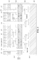
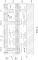
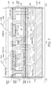
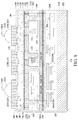
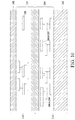
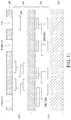
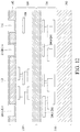
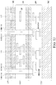
| US20160020170A1 (en) | 2014-07-17 | 2016-01-21 | Taiwan Semiconductor Manufacturing Company, Ltd. | Stacked integrated circuits with redistribution lines |
| US20160086997A1 (en) | 2011-04-19 | 2016-03-24 | Sony Corporation | Semiconductor device, manufacturing method thereof, solid-state imaging device, and electronic apparatus |
Family Cites Families (23)
| Publication number | Priority date | Publication date | Assignee | Title |
|---|---|---|---|---|
| US7642195B2 (en) | 2005-09-26 | 2010-01-05 | Applied Materials, Inc. | Hydrogen treatment to improve photoresist adhesion and rework consistency |
| KR100830581B1 (en) | 2006-11-06 | 2008-05-22 | 삼성전자주식회사 | Semiconductor device having through via and method for manufacturing the same |
| US7772123B2 (en) | 2008-06-06 | 2010-08-10 | Infineon Technologies Ag | Through substrate via semiconductor components |
| KR20100042021A (en) * | 2008-10-15 | 2010-04-23 | 삼성전자주식회사 | Semiconductor chip, stack module, memory card, and method of fabricating the semiconductor chip |
| US7875948B2 (en) | 2008-10-21 | 2011-01-25 | Jaroslav Hynecek | Backside illuminated image sensor |
| US8426938B2 (en) | 2009-02-16 | 2013-04-23 | Samsung Electronics Co., Ltd. | Image sensor and method of fabricating the same |
| US8487444B2 (en) * | 2009-03-06 | 2013-07-16 | Taiwan Semiconductor Manufacturing Company, Ltd. | Three-dimensional system-in-package architecture |
| US9406561B2 (en) | 2009-04-20 | 2016-08-02 | International Business Machines Corporation | Three dimensional integrated circuit integration using dielectric bonding first and through via formation last |
| US8502338B2 (en) | 2010-09-09 | 2013-08-06 | Taiwan Semiconductor Manufacturing Company, Ltd. | Through-substrate via waveguides |
| US8610259B2 (en) | 2010-09-17 | 2013-12-17 | Tessera, Inc. | Multi-function and shielded 3D interconnects |
| KR20120031811A (en) | 2010-09-27 | 2012-04-04 | 삼성전자주식회사 | Semiconductor devices and methods of fabricating the same |
| US8525343B2 (en) | 2010-09-28 | 2013-09-03 | Taiwan Semiconductor Manufacturing Company, Ltd. | Device with through-silicon via (TSV) and method of forming the same |
| US8492241B2 (en) | 2010-10-14 | 2013-07-23 | International Business Machines Corporation | Method for simultaneously forming a through silicon via and a deep trench structure |
| US8896125B2 (en) | 2011-07-05 | 2014-11-25 | Sony Corporation | Semiconductor device, fabrication method for a semiconductor device and electronic apparatus |
| US9076664B2 (en) | 2011-10-07 | 2015-07-07 | Freescale Semiconductor, Inc. | Stacked semiconductor die with continuous conductive vias |
| US9105628B1 (en) | 2012-03-29 | 2015-08-11 | Valery Dubin | Through substrate via (TSuV) structures and method of making the same |
| US8603893B1 (en) | 2012-05-17 | 2013-12-10 | GlobalFoundries, Inc. | Methods for fabricating FinFET integrated circuits on bulk semiconductor substrates |
| US8697515B2 (en) | 2012-06-06 | 2014-04-15 | Taiwan Semiconductor Manufacturing Company, Ltd. | Method of making a FinFET device |
| US8933544B2 (en) | 2012-07-12 | 2015-01-13 | Omnivision Technologies, Inc. | Integrated circuit stack with integrated electromagnetic interference shielding |
| KR102021884B1 (en) | 2012-09-25 | 2019-09-18 | 삼성전자주식회사 | Semiconductor Device Having Backside Bonding Structure |
| US8803328B1 (en) | 2013-01-22 | 2014-08-12 | International Business Machines Corporation | Random coded integrated circuit structures and methods of making random coded integrated circuit structures |
| US9455158B2 (en) | 2014-05-30 | 2016-09-27 | Taiwan Semiconductor Manufacturing Company, Ltd. | 3DIC interconnect devices and methods of forming same |
| TWI615976B (en) | 2014-07-07 | 2018-02-21 | 聯華電子股份有限公司 | Fin field effect transistor and method of manufacturing the same |
-
2014
- 2014-07-17 US US14/334,212 patent/US9449914B2/en active Active
- 2014-08-19 DE DE102014111783.2A patent/DE102014111783B4/en active Active
- 2014-11-04 TW TW103138143A patent/TWI553824B/en active
- 2014-12-26 KR KR1020140190863A patent/KR101690841B1/en active IP Right Grant
- 2014-12-30 CN CN201410844501.8A patent/CN105321903B/en active Active
-
2016
- 2016-09-19 US US15/269,431 patent/US10269768B2/en active Active
-
2019
- 2019-04-22 US US16/390,894 patent/US10629568B2/en active Active
-
2020
- 2020-04-20 US US16/853,293 patent/US11923338B2/en active Active
Patent Citations (100)
| Publication number | Priority date | Publication date | Assignee | Title |
|---|---|---|---|---|
| US4956312A (en) | 1988-06-06 | 1990-09-11 | U.S. Philips Corporation | Method of manufacturing a semiconductor device |
| US6207494B1 (en) | 1994-12-29 | 2001-03-27 | Infineon Technologies Corporation | Isolation collar nitride liner for DRAM process improvement |
| US6111319A (en) | 1995-12-19 | 2000-08-29 | Stmicroelectronics, Inc. | Method of forming submicron contacts and vias in an integrated circuit |
| US20020123219A1 (en) | 2001-03-02 | 2002-09-05 | Jerald Laverty | Method of forming a via of a dual damascene with low resistance |
| US7535920B2 (en) | 2002-07-08 | 2009-05-19 | Brooktree Broadband Holding, Inc. | Method and system for optimizing UTOPIA CLAV polling arbitration |
| US7453150B1 (en) | 2004-04-01 | 2008-11-18 | Rensselaer Polytechnic Institute | Three-dimensional face-to-face integration assembly |
| US7642173B2 (en) | 2004-04-01 | 2010-01-05 | Rensselaer Polytechnic Institute | Three-dimensional face-to-face integration assembly |
| US20060073695A1 (en) | 2004-09-30 | 2006-04-06 | International Business Machines Corporation | Gas dielectric structure forming methods |
| US20060286767A1 (en) * | 2005-06-17 | 2006-12-21 | Clarke Rowland C | Novel thinning process for 3 - dimensional integration via wafer bonding |
| US7485968B2 (en) | 2005-08-11 | 2009-02-03 | Ziptronix, Inc. | 3D IC method and device |
| US20100171196A1 (en) | 2005-08-26 | 2010-07-08 | Koninklijke Philips Electronics N.V. | Electrically shielded through-wafer interconnect |
| US20070117348A1 (en) | 2005-11-21 | 2007-05-24 | Shriram Ramanathan | 3D integrated circuits using thick metal for backside connections and offset bumps |
| US8125052B2 (en) | 2007-05-14 | 2012-02-28 | Taiwan Semiconductor Manufacturing Co., Ltd. | Seal ring structure with improved cracking protection |
| US20080284041A1 (en) | 2007-05-18 | 2008-11-20 | Samsung Electronics Co., Ltd. | Semiconductor package with through silicon via and related method of fabrication |
| US7973415B2 (en) | 2007-06-06 | 2011-07-05 | Renesas Electronics Corporation | Manufacturing process and structure of through silicon via |
| US20090014843A1 (en) | 2007-06-06 | 2009-01-15 | Kawashita Michihiro | Manufacturing process and structure of through silicon via |
| US8324736B2 (en) | 2007-06-06 | 2012-12-04 | Renesas Electronics Corporation | Manufacturing process and structure of through silicon via |
| JP2008305897A (en) | 2007-06-06 | 2008-12-18 | Renesas Technology Corp | Semiconductor device and manufacturing method thereof |
| US20090079077A1 (en) | 2007-09-20 | 2009-03-26 | International Business Machines Corporation | Interconnect structure with a via gouging feature absent profile damage to the interconnect dielectric and method of fabricating same |
| US20090134432A1 (en) | 2007-11-22 | 2009-05-28 | Kabushiki Kaisha Toshiba | Nonvolatile semiconductor memory device and method of manufacturing the same |
| US20090166840A1 (en) | 2007-12-27 | 2009-07-02 | Samsung Electronics Co., Ltd. | Wafer-level stack package |
| US8153521B2 (en) | 2007-12-27 | 2012-04-10 | Samsung Electronics Co., Ltd. | Wafer-level stack package |
| US8344514B2 (en) | 2008-06-03 | 2013-01-01 | Micron Technology, Inc. | Semiconductor device structures and electronic devices including same hybrid conductive vias |
| US20140175653A1 (en) | 2008-07-16 | 2014-06-26 | Micron Technology, Inc. | Semiconductor devices comprising interconnect structures and methods of fabrication |
| US20100090317A1 (en) | 2008-10-15 | 2010-04-15 | Bernd Zimmermann | Interconnect Structures and Methods |
| JP2010114165A (en) | 2008-11-04 | 2010-05-20 | Nikon Corp | Semiconductor device, laminated semiconductor device, and method for manufacturing laminated semiconductor device |
| US20100193964A1 (en) | 2009-02-03 | 2010-08-05 | International Business Machines Corporation | method of making 3d integrated circuits and structures formed thereby |
| US8158515B2 (en) | 2009-02-03 | 2012-04-17 | International Business Machines Corporation | Method of making 3D integrated circuits |
| US20100200833A1 (en) | 2009-02-06 | 2010-08-12 | Sim Kyu-Rie | Semiconductor device including uniform contact plugs and a method of manufacturing the same |
| KR20100094905A (en) | 2009-02-19 | 2010-08-27 | 이상윤 | Mass storage semiconductor memory device and method for fabricating the same |
| US20100224876A1 (en) | 2009-03-05 | 2010-09-09 | International Business Machines Corporation | Two-Sided Semiconductor Structure |
| US20100238331A1 (en) | 2009-03-19 | 2010-09-23 | Sony Corporation | Semiconductor device and method of manufacturing the same, and electronic apparatus |
| CN101840925A (en) | 2009-03-19 | 2010-09-22 | 索尼公司 | Semiconductor device and manufacture method thereof and electronic equipment |
| US8358008B2 (en) | 2009-07-13 | 2013-01-22 | Kabushiki Kaisha Toshiba | Semiconductor device |
| US20110062501A1 (en) | 2009-09-17 | 2011-03-17 | Globalfoundries Inc. | Method for self-aligning a stop layer to a replacement gate for self-aligned contact integration |
| US8581414B2 (en) | 2009-09-21 | 2013-11-12 | Kabushiki Kaisha Toshiba | Method of manufacturing three-dimensional integrated circuit and three-dimensional integrated circuit apparatus |
| WO2011033601A1 (en) | 2009-09-21 | 2011-03-24 | 株式会社 東芝 | Method and apparatus for manufacturing three-dimensional integrated circuit |
| US20110133339A1 (en) | 2009-12-03 | 2011-06-09 | Meng-Jen Wang | Semiconductor Structure and Method for Making the Same |
| US20110171827A1 (en) | 2010-01-14 | 2011-07-14 | International Business Machines Corporation | Three Dimensional Integration and Methods of Through Silicon Via Creation |
| US20110171582A1 (en) | 2010-01-14 | 2011-07-14 | International Business Machines Corporation | Three Dimensional Integration With Through Silicon Vias Having Multiple Diameters |
| US20110193197A1 (en) | 2010-02-05 | 2011-08-11 | International Business Machines Corporation | Structure and method for making crack stop for 3d integrated circuits |
| US8729711B2 (en) | 2010-02-23 | 2014-05-20 | Panasonic Corporation | Semiconductor device |
| US8692382B2 (en) | 2010-03-11 | 2014-04-08 | Yu-Lin Yen | Chip package |
| US8525345B2 (en) | 2010-03-11 | 2013-09-03 | Yu-Lin Yen | Chip package and method for forming the same |
| US20110221070A1 (en) | 2010-03-11 | 2011-09-15 | Yu-Lin Yen | Chip package and method for forming the same |
| US20120056323A1 (en) | 2010-06-22 | 2012-03-08 | Institute of Microelectronics, Chinese Academy of Sciences | Semiconductor structure and method for manufacturing the same |
| CN102299133A (en) | 2010-06-22 | 2011-12-28 | 中国科学院微电子研究所 | Semiconductor structure and manufacturing method thereof |
| US8415806B2 (en) | 2010-06-22 | 2013-04-09 | Institute of Microelectronics, Chinese Academy of Sciences | Semiconductor structure and method for manufacturing the same |
| WO2012006766A1 (en) | 2010-07-14 | 2012-01-19 | 中国科学院微电子研究所 | Semiconductor structure and manufacturing method thereof |
| CN102339813A (en) | 2010-07-14 | 2012-02-01 | 中国科学院微电子研究所 | Semiconductor structure and manufacturing method thereof |
| US20120038020A1 (en) | 2010-08-13 | 2012-02-16 | Taiwan Semiconductor Manufacturing Company, Ltd. | Seal ring structure with metal pad |
| US20120038028A1 (en) | 2010-08-13 | 2012-02-16 | Taiwan Semiconductor Manufacturing Company, Ltd. | Multiple seal ring structure |
| US20120056330A1 (en) | 2010-09-07 | 2012-03-08 | Samsung Electronics Co., Ltd. | Semiconductor device |
| US8421193B2 (en) | 2010-11-18 | 2013-04-16 | Nanya Technology Corporation | Integrated circuit device having through via and method for preparing the same |
| CN102468279A (en) | 2010-11-18 | 2012-05-23 | 南亚科技股份有限公司 | Integrated circuit device and method for preparing the same |
| US20130140680A1 (en) | 2010-11-19 | 2013-06-06 | Panasonic Corporation | Semiconductor device |
| US8592991B2 (en) | 2010-11-29 | 2013-11-26 | Samsung Electronics Co., Ltd. | Semiconductor device, fabricating method thereof and semiconductor package including the semiconductor device |
| CN102569314A (en) | 2010-12-15 | 2012-07-11 | 索尼公司 | Semiconductor Device, Manufacturing Method Thereof, And Electronic Apparatus |
| US20120181698A1 (en) | 2011-01-18 | 2012-07-19 | Hong Kong Applied Science and Technology Research Institute Company Limited | Forming through-silicon-vias for multi-wafer integrated circuits |
| US20120193785A1 (en) * | 2011-02-01 | 2012-08-02 | Megica Corporation | Multichip Packages |
| US20120261827A1 (en) | 2011-04-13 | 2012-10-18 | Taiwan Semiconductor Manufacturing Company, Ltd. | Through-silicon vias for semicondcutor substrate and method of manufacture |
| US20160086997A1 (en) | 2011-04-19 | 2016-03-24 | Sony Corporation | Semiconductor device, manufacturing method thereof, solid-state imaging device, and electronic apparatus |
| US20120292730A1 (en) | 2011-05-20 | 2012-11-22 | Taiwan Semiconductor Manufacturing Company, Ltd. | Semiconductor Device Having a Bonding Pad and Method of Manufacturing The Same |
| KR20140000719A (en) | 2011-06-02 | 2014-01-03 | 마이크론 테크놀로지, 인크. | Conductive structures, systems and devices including conductive structures and related methods |
| CN102867777A (en) | 2011-07-07 | 2013-01-09 | 台湾积体电路制造股份有限公司 | Forming grounded through-silicon vias in a semiconductor substrate |
| US20130009317A1 (en) | 2011-07-07 | 2013-01-10 | Taiwan Semiconductor Manufacturing Company, Ltd. | Forming grounded through-silicon vias in a semiconductor substrate |
| US8872345B2 (en) | 2011-07-07 | 2014-10-28 | Taiwan Semiconductor Manufacturing Company, Ltd. | Forming grounded through-silicon vias in a semiconductor substrate |
| CN103000593A (en) | 2011-09-09 | 2013-03-27 | 台湾积体电路制造股份有限公司 | Packaging methods and structures for semiconductor devices |
| US8884431B2 (en) | 2011-09-09 | 2014-11-11 | Taiwan Semiconductor Manufacturing Company, Ltd. | Packaging methods and structures for semiconductor devices |
| US20130093098A1 (en) | 2011-10-13 | 2013-04-18 | Taiwan Semiconductor Manufacturing Company, Ltd. | Through substrate via structures and methods of forming the same |
| US20150137238A1 (en) | 2012-02-08 | 2015-05-21 | Sony Corporation | High-frequency semiconductor device and method of manufacturing the same |
| US20130264688A1 (en) * | 2012-04-06 | 2013-10-10 | Omnivision Technologies, Inc. | Method and apparatus providing integrated circuit system with interconnected stacked device wafers |
| CN103367348A (en) | 2012-04-06 | 2013-10-23 | 全视科技有限公司 | Method and apparatus providing integrated circuit system with interconnected stacked device wafers |
| KR20130116607A (en) | 2012-04-16 | 2013-10-24 | 삼성전자주식회사 | Three dimensional semiconductor memory device and method of fabricating the same |
| US20130270625A1 (en) | 2012-04-16 | 2013-10-17 | Byong-hyun JANG | Three-dimensional semiconductor memory devices and methods of fabricating the same |
| US20130292794A1 (en) | 2012-05-02 | 2013-11-07 | Taiwan Semiconductor Manufacturing Company, Ltd. | Semiconductor device and method of fabricating |
| US8643074B2 (en) | 2012-05-02 | 2014-02-04 | Taiwan Semiconductor Manufacturing Company, Ltd. | Semiconductor device |
| JP2013251511A (en) | 2012-06-04 | 2013-12-12 | Macronix Internatl Co Ltd | Method for manufacturing 3d stacked multichip module |
| US20140070426A1 (en) | 2012-09-12 | 2014-03-13 | Jae-hwa Park | Integrated circuit devices including a via structure and methods of fabricating integrated circuit devices including a via structure |
| US20140247380A1 (en) | 2013-03-01 | 2014-09-04 | Aptina Imaging Corporation | Image sensor pixels with self-aligned lateral anti-blooming structures |
| US20140264709A1 (en) | 2013-03-12 | 2014-09-18 | Taiwan Semiconductor Manufacturing Company, Ltd. | Interconnect Structure for Connecting Dies and Methods of Forming the Same |
| US20150187701A1 (en) | 2013-03-12 | 2015-07-02 | Taiwan Semiconductor Manufacturing Company, Ltd. | Semiconductor Devices and Methods of Manufacture Thereof |
| US20140264862A1 (en) | 2013-03-12 | 2014-09-18 | Taiwan Semiconductor Manufacturing Company, Ltd. | Interconnect Structure and Method |
| CN104051414A (en) | 2013-03-12 | 2014-09-17 | 台湾积体电路制造股份有限公司 | Interconnect Structure and Method |
| US20140264947A1 (en) | 2013-03-13 | 2014-09-18 | Taiwan Semiconductor Manufacturing Company, Ltd. | Interconnect Apparatus and Method |
| US20140264911A1 (en) | 2013-03-15 | 2014-09-18 | Globalfoundries Singapore Pte. Ltd. | Through silicon vias |
| US20140361352A1 (en) | 2013-06-06 | 2014-12-11 | United Microelectronics Corp. | Semiconductor device and fabrication method thereof |
| US9006804B2 (en) | 2013-06-06 | 2015-04-14 | United Microelectronics Corp. | Semiconductor device and fabrication method thereof |
| US20140361347A1 (en) | 2013-06-10 | 2014-12-11 | United Microelectronics Corp. | Stacked wafer structure and fabricating method thereof |
| US9059696B1 (en) | 2013-08-01 | 2015-06-16 | Altera Corporation | Interposer with programmable power gating granularity |
| US20150129942A1 (en) | 2013-11-13 | 2015-05-14 | United Microelectronics Corp. | Semiconductor structure and method for manufacturing the same |
| US20150179613A1 (en) | 2013-12-19 | 2015-06-25 | Taiwan Semiconductor Manufacturing Company, Ltd. | 3DIC Interconnect Apparatus and Method |
| US20150179612A1 (en) | 2013-12-19 | 2015-06-25 | Taiwan Semiconductor Manufacturing Company, Ltd. | 3DIC Interconnect Apparatus and Method |
| US20150221695A1 (en) | 2014-02-03 | 2015-08-06 | Samsung Electronics Co., Ltd. | Via structures including etch-delay structures and semiconductor devices having via plugs |
| US20150228584A1 (en) | 2014-02-13 | 2015-08-13 | Taiwan Semiconductor Manufacturing Company, Ltd. | Multi-via interconnect structure and method of manufacture |
| US20150243582A1 (en) | 2014-02-21 | 2015-08-27 | Globalfoundries Inc. | New process flow for a combined ca and tsv oxide deposition |
| US9192016B1 (en) | 2014-05-22 | 2015-11-17 | Cree, Inc. | Lighting apparatus with inductor current limiting for noise reduction |
| US20150348917A1 (en) | 2014-05-29 | 2015-12-03 | Taiwan Semiconductor Manufacturing Company, Ltd. | 3DIC Interconnect Devices and Methods of Forming Same |
| US20150348874A1 (en) | 2014-05-29 | 2015-12-03 | Taiwan Semiconductor Manufacturing Company, Ltd. | 3DIC Interconnect Devices and Methods of Forming Same |
| US20160020170A1 (en) | 2014-07-17 | 2016-01-21 | Taiwan Semiconductor Manufacturing Company, Ltd. | Stacked integrated circuits with redistribution lines |
Non-Patent Citations (1)
| Title |
|---|
| Quirk, Michael et al., "Semiconductor Manufacturing Process," 2001, Prentice-Hall, Inc, Chapter 12, p. 300. |
Cited By (1)
| Publication number | Priority date | Publication date | Assignee | Title |
|---|---|---|---|---|
| US11569149B1 (en) | 2021-07-09 | 2023-01-31 | Changxin Memory Technologies, Inc. | Semiconductor structure and manufacturing method thereof |
Also Published As
| Publication number | Publication date |
|---|---|
| US20200258865A1 (en) | 2020-08-13 |
| DE102014111783A1 (en) | 2016-01-21 |
| US20170005076A1 (en) | 2017-01-05 |
| US10269768B2 (en) | 2019-04-23 |
| CN105321903B (en) | 2018-12-14 |
| KR101690841B1 (en) | 2017-01-09 |
| US20160020170A1 (en) | 2016-01-21 |
| TW201605012A (en) | 2016-02-01 |
| CN105321903A (en) | 2016-02-10 |
| US20190252354A1 (en) | 2019-08-15 |
| TWI553824B (en) | 2016-10-11 |
| US9449914B2 (en) | 2016-09-20 |
| KR20160010274A (en) | 2016-01-27 |
| DE102014111783B4 (en) | 2020-08-27 |
| US11923338B2 (en) | 2024-03-05 |
Similar Documents
| Publication | Publication Date | Title |
|---|---|---|
| US10629568B2 (en) | Stacked integrated circuits with redistribution lines | |
| US11596800B2 (en) | Interconnect structure and method of forming same | |
| US9941249B2 (en) | Multi-wafer stacking by Ox-Ox bonding | |
| US9553020B2 (en) | Interconnect structure for connecting dies and methods of forming the same | |
| US9978708B2 (en) | Wafer backside interconnect structure connected to TSVs | |
| US9543257B2 (en) | 3DIC interconnect devices and methods of forming same | |
| US10361234B2 (en) | 3DIC interconnect apparatus and method | |
| US8836085B2 (en) | Cost-effective TSV formation | |
| US9041206B2 (en) | Interconnect structure and method | |
| US20150348874A1 (en) | 3DIC Interconnect Devices and Methods of Forming Same | |
| US9437578B2 (en) | Stacked IC control through the use of homogenous region | |
| US20230201613A1 (en) | Interconnect Structure and Method of Forming Same |
Legal Events
| Date | Code | Title | Description |
|---|---|---|---|
| FEPP | Fee payment procedure |
Free format text: ENTITY STATUS SET TO UNDISCOUNTED (ORIGINAL EVENT CODE: BIG.); ENTITY STATUS OF PATENT OWNER: LARGE ENTITY |
|
| STPP | Information on status: patent application and granting procedure in general |
Free format text: DOCKETED NEW CASE - READY FOR EXAMINATION |
|
| STPP | Information on status: patent application and granting procedure in general |
Free format text: NON FINAL ACTION MAILED |
|
| STPP | Information on status: patent application and granting procedure in general |
Free format text: RESPONSE TO NON-FINAL OFFICE ACTION ENTERED AND FORWARDED TO EXAMINER |
|
| STPP | Information on status: patent application and granting procedure in general |
Free format text: NOTICE OF ALLOWANCE MAILED -- APPLICATION RECEIVED IN OFFICE OF PUBLICATIONS |
|
| STCF | Information on status: patent grant |
Free format text: PATENTED CASE |
|
| MAFP | Maintenance fee payment |
Free format text: PAYMENT OF MAINTENANCE FEE, 4TH YEAR, LARGE ENTITY (ORIGINAL EVENT CODE: M1551); ENTITY STATUS OF PATENT OWNER: LARGE ENTITY Year of fee payment: 4 |