RU2430832C2 - Method of processing by preset wave length laser radiation and system to this end - Google Patents
Method of processing by preset wave length laser radiation and system to this end Download PDFInfo
- Publication number
- RU2430832C2 RU2430832C2 RU2008151925/05A RU2008151925A RU2430832C2 RU 2430832 C2 RU2430832 C2 RU 2430832C2 RU 2008151925/05 A RU2008151925/05 A RU 2008151925/05A RU 2008151925 A RU2008151925 A RU 2008151925A RU 2430832 C2 RU2430832 C2 RU 2430832C2
- Authority
- RU
- Russia
- Prior art keywords
- radiation
- energy
- laser
- devices
- temperature
- Prior art date
Links
- 238000012545 processing Methods 0.000 title claims abstract description 26
- 230000005855 radiation Effects 0.000 title claims description 122
- 238000000034 method Methods 0.000 title claims description 109
- 238000010438 heat treatment Methods 0.000 claims abstract description 135
- 239000000463 material Substances 0.000 claims description 94
- 239000011159 matrix material Substances 0.000 claims description 58
- 238000005516 engineering process Methods 0.000 claims description 45
- 238000000071 blow moulding Methods 0.000 claims description 43
- 238000010521 absorption reaction Methods 0.000 claims description 40
- VYPSYNLAJGMNEJ-UHFFFAOYSA-N silicon dioxide Inorganic materials O=[Si]=O VYPSYNLAJGMNEJ-UHFFFAOYSA-N 0.000 claims description 34
- 239000010453 quartz Substances 0.000 claims description 31
- 230000008569 process Effects 0.000 claims description 25
- 230000005540 biological transmission Effects 0.000 claims description 21
- 230000033001 locomotion Effects 0.000 claims description 21
- 238000001816 cooling Methods 0.000 claims description 17
- 238000012544 monitoring process Methods 0.000 claims description 17
- 238000009434 installation Methods 0.000 claims description 14
- 239000004033 plastic Substances 0.000 claims description 14
- 229920003023 plastic Polymers 0.000 claims description 14
- 238000006243 chemical reaction Methods 0.000 claims description 12
- 230000008859 change Effects 0.000 claims description 11
- 238000009826 distribution Methods 0.000 claims description 10
- 230000001678 irradiating effect Effects 0.000 claims description 8
- 229920001169 thermoplastic Polymers 0.000 claims description 8
- 239000004416 thermosoftening plastic Substances 0.000 claims description 8
- 238000000465 moulding Methods 0.000 claims description 7
- 230000001360 synchronised effect Effects 0.000 claims description 7
- 230000015572 biosynthetic process Effects 0.000 claims description 6
- 238000005457 optimization Methods 0.000 claims description 6
- 239000007788 liquid Substances 0.000 claims description 5
- 239000000203 mixture Substances 0.000 claims description 5
- 230000035515 penetration Effects 0.000 claims description 4
- 239000012815 thermoplastic material Substances 0.000 claims description 4
- 238000003491 array Methods 0.000 claims description 3
- 238000005259 measurement Methods 0.000 claims description 3
- 125000004122 cyclic group Chemical group 0.000 claims description 2
- 230000028016 temperature homeostasis Effects 0.000 claims description 2
- 230000001351 cycling effect Effects 0.000 claims 1
- 230000017525 heat dissipation Effects 0.000 claims 1
- 238000003331 infrared imaging Methods 0.000 claims 1
- 230000000694 effects Effects 0.000 abstract description 4
- 239000000126 substance Substances 0.000 abstract description 3
- 230000004936 stimulating effect Effects 0.000 abstract description 2
- 238000010327 methods by industry Methods 0.000 abstract 1
- 239000010410 layer Substances 0.000 description 231
- 239000004065 semiconductor Substances 0.000 description 55
- 239000013078 crystal Substances 0.000 description 38
- 239000002096 quantum dot Substances 0.000 description 36
- 239000000758 substrate Substances 0.000 description 32
- 238000004519 manufacturing process Methods 0.000 description 31
- 229920000139 polyethylene terephthalate Polymers 0.000 description 29
- 239000005020 polyethylene terephthalate Substances 0.000 description 29
- GPXJNWSHGFTCBW-UHFFFAOYSA-N Indium phosphide Chemical compound [In]#P GPXJNWSHGFTCBW-UHFFFAOYSA-N 0.000 description 24
- 239000012535 impurity Substances 0.000 description 20
- 238000011282 treatment Methods 0.000 description 20
- 238000012546 transfer Methods 0.000 description 16
- 238000001746 injection moulding Methods 0.000 description 14
- 230000008901 benefit Effects 0.000 description 11
- 238000010411 cooking Methods 0.000 description 11
- 238000013461 design Methods 0.000 description 11
- 230000005670 electromagnetic radiation Effects 0.000 description 11
- 238000001228 spectrum Methods 0.000 description 11
- 230000007423 decrease Effects 0.000 description 10
- 229910052738 indium Inorganic materials 0.000 description 10
- RPQDHPTXJYYUPQ-UHFFFAOYSA-N indium arsenide Chemical compound [In]#[As] RPQDHPTXJYYUPQ-UHFFFAOYSA-N 0.000 description 10
- APFVFJFRJDLVQX-UHFFFAOYSA-N indium atom Chemical compound [In] APFVFJFRJDLVQX-UHFFFAOYSA-N 0.000 description 10
- 229910000673 Indium arsenide Inorganic materials 0.000 description 9
- 229910052785 arsenic Inorganic materials 0.000 description 9
- RQNWIZPPADIBDY-UHFFFAOYSA-N arsenic atom Chemical compound [As] RQNWIZPPADIBDY-UHFFFAOYSA-N 0.000 description 9
- 235000013305 food Nutrition 0.000 description 9
- 238000013459 approach Methods 0.000 description 8
- 230000003750 conditioning effect Effects 0.000 description 8
- 230000006870 function Effects 0.000 description 8
- 230000003287 optical effect Effects 0.000 description 8
- 239000004020 conductor Substances 0.000 description 7
- 238000005265 energy consumption Methods 0.000 description 7
- 230000001276 controlling effect Effects 0.000 description 6
- 239000002019 doping agent Substances 0.000 description 6
- XLYOFNOQVPJJNP-UHFFFAOYSA-N water Substances O XLYOFNOQVPJJNP-UHFFFAOYSA-N 0.000 description 6
- XUIMIQQOPSSXEZ-UHFFFAOYSA-N Silicon Chemical compound [Si] XUIMIQQOPSSXEZ-UHFFFAOYSA-N 0.000 description 5
- 239000000853 adhesive Substances 0.000 description 5
- 230000001070 adhesive effect Effects 0.000 description 5
- JNDMLEXHDPKVFC-UHFFFAOYSA-N aluminum;oxygen(2-);yttrium(3+) Chemical compound [O-2].[O-2].[O-2].[Al+3].[Y+3] JNDMLEXHDPKVFC-UHFFFAOYSA-N 0.000 description 5
- 238000000576 coating method Methods 0.000 description 5
- PCHJSUWPFVWCPO-UHFFFAOYSA-N gold Chemical compound [Au] PCHJSUWPFVWCPO-UHFFFAOYSA-N 0.000 description 5
- 239000010931 gold Substances 0.000 description 5
- 238000002360 preparation method Methods 0.000 description 5
- 229910052710 silicon Inorganic materials 0.000 description 5
- 239000010703 silicon Substances 0.000 description 5
- 229910019901 yttrium aluminum garnet Inorganic materials 0.000 description 5
- 229910000530 Gallium indium arsenide Inorganic materials 0.000 description 4
- HCHKCACWOHOZIP-UHFFFAOYSA-N Zinc Chemical compound [Zn] HCHKCACWOHOZIP-UHFFFAOYSA-N 0.000 description 4
- 230000004888 barrier function Effects 0.000 description 4
- 239000011248 coating agent Substances 0.000 description 4
- 230000006378 damage Effects 0.000 description 4
- 238000001035 drying Methods 0.000 description 4
- 230000005611 electricity Effects 0.000 description 4
- 229910052737 gold Inorganic materials 0.000 description 4
- 230000035876 healing Effects 0.000 description 4
- 238000002329 infrared spectrum Methods 0.000 description 4
- 238000013021 overheating Methods 0.000 description 4
- -1 polyethylene terephthalate Polymers 0.000 description 4
- 238000009736 wetting Methods 0.000 description 4
- 229910052725 zinc Inorganic materials 0.000 description 4
- 239000011701 zinc Substances 0.000 description 4
- 241001465754 Metazoa Species 0.000 description 3
- KXNLCSXBJCPWGL-UHFFFAOYSA-N [Ga].[As].[In] Chemical compound [Ga].[As].[In] KXNLCSXBJCPWGL-UHFFFAOYSA-N 0.000 description 3
- 238000007664 blowing Methods 0.000 description 3
- 239000003795 chemical substances by application Substances 0.000 description 3
- RZVXOCDCIIFGGH-UHFFFAOYSA-N chromium gold Chemical compound [Cr].[Au] RZVXOCDCIIFGGH-UHFFFAOYSA-N 0.000 description 3
- 150000001875 compounds Chemical class 0.000 description 3
- 230000009931 harmful effect Effects 0.000 description 3
- 230000006872 improvement Effects 0.000 description 3
- 210000000056 organ Anatomy 0.000 description 3
- 238000003672 processing method Methods 0.000 description 3
- 230000010349 pulsation Effects 0.000 description 3
- 238000003303 reheating Methods 0.000 description 3
- 239000007787 solid Substances 0.000 description 3
- 239000000243 solution Substances 0.000 description 3
- 238000003860 storage Methods 0.000 description 3
- 230000007704 transition Effects 0.000 description 3
- JBRZTFJDHDCESZ-UHFFFAOYSA-N AsGa Chemical compound [As]#[Ga] JBRZTFJDHDCESZ-UHFFFAOYSA-N 0.000 description 2
- 229910000990 Ni alloy Inorganic materials 0.000 description 2
- 229910001297 Zn alloy Inorganic materials 0.000 description 2
- BYDQGSVXQDOSJJ-UHFFFAOYSA-N [Ge].[Au] Chemical compound [Ge].[Au] BYDQGSVXQDOSJJ-UHFFFAOYSA-N 0.000 description 2
- 239000006096 absorbing agent Substances 0.000 description 2
- 230000009471 action Effects 0.000 description 2
- 238000007792 addition Methods 0.000 description 2
- 230000002411 adverse Effects 0.000 description 2
- 229910052782 aluminium Inorganic materials 0.000 description 2
- XAGFODPZIPBFFR-UHFFFAOYSA-N aluminium Chemical compound [Al] XAGFODPZIPBFFR-UHFFFAOYSA-N 0.000 description 2
- 235000013361 beverage Nutrition 0.000 description 2
- 238000009529 body temperature measurement Methods 0.000 description 2
- 238000005253 cladding Methods 0.000 description 2
- 239000002826 coolant Substances 0.000 description 2
- 230000007547 defect Effects 0.000 description 2
- 238000010586 diagram Methods 0.000 description 2
- 201000010099 disease Diseases 0.000 description 2
- 208000037265 diseases, disorders, signs and symptoms Diseases 0.000 description 2
- 230000007613 environmental effect Effects 0.000 description 2
- 239000000835 fiber Substances 0.000 description 2
- 230000004907 flux Effects 0.000 description 2
- 239000003292 glue Substances 0.000 description 2
- MSNOMDLPLDYDME-UHFFFAOYSA-N gold nickel Chemical compound [Ni].[Au] MSNOMDLPLDYDME-UHFFFAOYSA-N 0.000 description 2
- 230000010354 integration Effects 0.000 description 2
- 230000004048 modification Effects 0.000 description 2
- 238000012986 modification Methods 0.000 description 2
- 239000003973 paint Substances 0.000 description 2
- 230000009467 reduction Effects 0.000 description 2
- 238000011160 research Methods 0.000 description 2
- 230000004044 response Effects 0.000 description 2
- 230000003595 spectral effect Effects 0.000 description 2
- 230000000638 stimulation Effects 0.000 description 2
- 230000001225 therapeutic effect Effects 0.000 description 2
- 238000011269 treatment regimen Methods 0.000 description 2
- 230000000007 visual effect Effects 0.000 description 2
- 229910001020 Au alloy Inorganic materials 0.000 description 1
- OKTJSMMVPCPJKN-UHFFFAOYSA-N Carbon Chemical compound [C] OKTJSMMVPCPJKN-UHFFFAOYSA-N 0.000 description 1
- VYZAMTAEIAYCRO-UHFFFAOYSA-N Chromium Chemical compound [Cr] VYZAMTAEIAYCRO-UHFFFAOYSA-N 0.000 description 1
- RYGMFSIKBFXOCR-UHFFFAOYSA-N Copper Chemical compound [Cu] RYGMFSIKBFXOCR-UHFFFAOYSA-N 0.000 description 1
- 229910000599 Cr alloy Inorganic materials 0.000 description 1
- 208000032131 Diabetic Neuropathies Diseases 0.000 description 1
- 102000004190 Enzymes Human genes 0.000 description 1
- 108090000790 Enzymes Proteins 0.000 description 1
- GYHNNYVSQQEPJS-UHFFFAOYSA-N Gallium Chemical compound [Ga] GYHNNYVSQQEPJS-UHFFFAOYSA-N 0.000 description 1
- 229910001218 Gallium arsenide Inorganic materials 0.000 description 1
- 229910000927 Ge alloy Inorganic materials 0.000 description 1
- 206010061218 Inflammation Diseases 0.000 description 1
- FYYHWMGAXLPEAU-UHFFFAOYSA-N Magnesium Chemical compound [Mg] FYYHWMGAXLPEAU-UHFFFAOYSA-N 0.000 description 1
- 206010028813 Nausea Diseases 0.000 description 1
- 238000001069 Raman spectroscopy Methods 0.000 description 1
- BUGBHKTXTAQXES-UHFFFAOYSA-N Selenium Chemical compound [Se] BUGBHKTXTAQXES-UHFFFAOYSA-N 0.000 description 1
- NINIDFKCEFEMDL-UHFFFAOYSA-N Sulfur Chemical compound [S] NINIDFKCEFEMDL-UHFFFAOYSA-N 0.000 description 1
- ATJFFYVFTNAWJD-UHFFFAOYSA-N Tin Chemical compound [Sn] ATJFFYVFTNAWJD-UHFFFAOYSA-N 0.000 description 1
- RTAQQCXQSZGOHL-UHFFFAOYSA-N Titanium Chemical compound [Ti] RTAQQCXQSZGOHL-UHFFFAOYSA-N 0.000 description 1
- 238000000862 absorption spectrum Methods 0.000 description 1
- 238000004378 air conditioning Methods 0.000 description 1
- AJGDITRVXRPLBY-UHFFFAOYSA-N aluminum indium Chemical compound [Al].[In] AJGDITRVXRPLBY-UHFFFAOYSA-N 0.000 description 1
- 230000009286 beneficial effect Effects 0.000 description 1
- 229910052790 beryllium Inorganic materials 0.000 description 1
- ATBAMAFKBVZNFJ-UHFFFAOYSA-N beryllium atom Chemical compound [Be] ATBAMAFKBVZNFJ-UHFFFAOYSA-N 0.000 description 1
- 229910052793 cadmium Inorganic materials 0.000 description 1
- BDOSMKKIYDKNTQ-UHFFFAOYSA-N cadmium atom Chemical compound [Cd] BDOSMKKIYDKNTQ-UHFFFAOYSA-N 0.000 description 1
- 229910052799 carbon Inorganic materials 0.000 description 1
- 235000014171 carbonated beverage Nutrition 0.000 description 1
- 239000000969 carrier Substances 0.000 description 1
- 239000013043 chemical agent Substances 0.000 description 1
- 229910052804 chromium Inorganic materials 0.000 description 1
- 239000011651 chromium Substances 0.000 description 1
- 239000000788 chromium alloy Substances 0.000 description 1
- 230000015271 coagulation Effects 0.000 description 1
- 238000005345 coagulation Methods 0.000 description 1
- 230000001427 coherent effect Effects 0.000 description 1
- 238000002485 combustion reaction Methods 0.000 description 1
- 230000000052 comparative effect Effects 0.000 description 1
- 238000000748 compression moulding Methods 0.000 description 1
- 229910052802 copper Inorganic materials 0.000 description 1
- 239000010949 copper Substances 0.000 description 1
- 230000006866 deterioration Effects 0.000 description 1
- 230000001627 detrimental effect Effects 0.000 description 1
- 239000003989 dielectric material Substances 0.000 description 1
- 239000003814 drug Substances 0.000 description 1
- 210000002310 elbow joint Anatomy 0.000 description 1
- 230000005684 electric field Effects 0.000 description 1
- 238000000295 emission spectrum Methods 0.000 description 1
- 206010015037 epilepsy Diseases 0.000 description 1
- 238000000407 epitaxy Methods 0.000 description 1
- 230000005284 excitation Effects 0.000 description 1
- 238000010101 extrusion blow moulding Methods 0.000 description 1
- 229910052733 gallium Inorganic materials 0.000 description 1
- 229910052732 germanium Inorganic materials 0.000 description 1
- GNPVGFCGXDBREM-UHFFFAOYSA-N germanium atom Chemical compound [Ge] GNPVGFCGXDBREM-UHFFFAOYSA-N 0.000 description 1
- 239000011521 glass Substances 0.000 description 1
- SAOPTAQUONRHEV-UHFFFAOYSA-N gold zinc Chemical compound [Zn].[Au] SAOPTAQUONRHEV-UHFFFAOYSA-N 0.000 description 1
- 208000014617 hemorrhoid Diseases 0.000 description 1
- 239000005556 hormone Substances 0.000 description 1
- 229940088597 hormone Drugs 0.000 description 1
- 239000012770 industrial material Substances 0.000 description 1
- 230000004054 inflammatory process Effects 0.000 description 1
- 239000004615 ingredient Substances 0.000 description 1
- 239000007924 injection Substances 0.000 description 1
- 238000010102 injection blow moulding Methods 0.000 description 1
- 238000010030 laminating Methods 0.000 description 1
- 238000004093 laser heating Methods 0.000 description 1
- 230000031700 light absorption Effects 0.000 description 1
- 229910052749 magnesium Inorganic materials 0.000 description 1
- 239000011777 magnesium Substances 0.000 description 1
- 238000007726 management method Methods 0.000 description 1
- 239000007769 metal material Substances 0.000 description 1
- 238000002488 metal-organic chemical vapour deposition Methods 0.000 description 1
- 239000011859 microparticle Substances 0.000 description 1
- 230000008693 nausea Effects 0.000 description 1
- 239000011368 organic material Substances 0.000 description 1
- 125000002524 organometallic group Chemical group 0.000 description 1
- 230000000149 penetrating effect Effects 0.000 description 1
- 230000010287 polarization Effects 0.000 description 1
- 229920000642 polymer Polymers 0.000 description 1
- 230000035484 reaction time Effects 0.000 description 1
- 230000001105 regulatory effect Effects 0.000 description 1
- 229920006395 saturated elastomer Polymers 0.000 description 1
- 229910052711 selenium Inorganic materials 0.000 description 1
- 239000011669 selenium Substances 0.000 description 1
- 239000000377 silicon dioxide Substances 0.000 description 1
- 239000002356 single layer Substances 0.000 description 1
- 239000007921 spray Substances 0.000 description 1
- 230000006641 stabilisation Effects 0.000 description 1
- 238000011105 stabilization Methods 0.000 description 1
- 239000010421 standard material Substances 0.000 description 1
- 239000007858 starting material Substances 0.000 description 1
- 229910052717 sulfur Inorganic materials 0.000 description 1
- 239000011593 sulfur Substances 0.000 description 1
- 238000004381 surface treatment Methods 0.000 description 1
- 239000000725 suspension Substances 0.000 description 1
- 239000013077 target material Substances 0.000 description 1
- 229910052714 tellurium Inorganic materials 0.000 description 1
- PORWMNRCUJJQNO-UHFFFAOYSA-N tellurium atom Chemical compound [Te] PORWMNRCUJJQNO-UHFFFAOYSA-N 0.000 description 1
- 238000002560 therapeutic procedure Methods 0.000 description 1
- 229910052718 tin Inorganic materials 0.000 description 1
- 230000000451 tissue damage Effects 0.000 description 1
- 231100000827 tissue damage Toxicity 0.000 description 1
- 229910052719 titanium Inorganic materials 0.000 description 1
- 239000010936 titanium Substances 0.000 description 1
- 238000000411 transmission spectrum Methods 0.000 description 1
- 238000002834 transmittance Methods 0.000 description 1
- 238000001429 visible spectrum Methods 0.000 description 1
- 238000010792 warming Methods 0.000 description 1
- 239000002699 waste material Substances 0.000 description 1
Images


Classifications
-
- B—PERFORMING OPERATIONS; TRANSPORTING
- B29—WORKING OF PLASTICS; WORKING OF SUBSTANCES IN A PLASTIC STATE IN GENERAL
- B29C—SHAPING OR JOINING OF PLASTICS; SHAPING OF MATERIAL IN A PLASTIC STATE, NOT OTHERWISE PROVIDED FOR; AFTER-TREATMENT OF THE SHAPED PRODUCTS, e.g. REPAIRING
- B29C49/00—Blow-moulding, i.e. blowing a preform or parison to a desired shape within a mould; Apparatus therefor
- B29C49/42—Component parts, details or accessories; Auxiliary operations
- B29C49/64—Heating or cooling preforms, parisons or blown articles
-
- B—PERFORMING OPERATIONS; TRANSPORTING
- B29—WORKING OF PLASTICS; WORKING OF SUBSTANCES IN A PLASTIC STATE IN GENERAL
- B29B—PREPARATION OR PRETREATMENT OF THE MATERIAL TO BE SHAPED; MAKING GRANULES OR PREFORMS; RECOVERY OF PLASTICS OR OTHER CONSTITUENTS OF WASTE MATERIAL CONTAINING PLASTICS
- B29B13/00—Conditioning or physical treatment of the material to be shaped
- B29B13/02—Conditioning or physical treatment of the material to be shaped by heating
- B29B13/023—Half-products, e.g. films, plates
- B29B13/024—Hollow bodies, e.g. tubes or profiles
-
- B—PERFORMING OPERATIONS; TRANSPORTING
- B29—WORKING OF PLASTICS; WORKING OF SUBSTANCES IN A PLASTIC STATE IN GENERAL
- B29C—SHAPING OR JOINING OF PLASTICS; SHAPING OF MATERIAL IN A PLASTIC STATE, NOT OTHERWISE PROVIDED FOR; AFTER-TREATMENT OF THE SHAPED PRODUCTS, e.g. REPAIRING
- B29C48/00—Extrusion moulding, i.e. expressing the moulding material through a die or nozzle which imparts the desired form; Apparatus therefor
- B29C48/25—Component parts, details or accessories; Auxiliary operations
- B29C48/92—Measuring, controlling or regulating
-
- B—PERFORMING OPERATIONS; TRANSPORTING
- B29—WORKING OF PLASTICS; WORKING OF SUBSTANCES IN A PLASTIC STATE IN GENERAL
- B29C—SHAPING OR JOINING OF PLASTICS; SHAPING OF MATERIAL IN A PLASTIC STATE, NOT OTHERWISE PROVIDED FOR; AFTER-TREATMENT OF THE SHAPED PRODUCTS, e.g. REPAIRING
- B29C49/00—Blow-moulding, i.e. blowing a preform or parison to a desired shape within a mould; Apparatus therefor
- B29C49/42—Component parts, details or accessories; Auxiliary operations
- B29C49/78—Measuring, controlling or regulating
-
- H—ELECTRICITY
- H05—ELECTRIC TECHNIQUES NOT OTHERWISE PROVIDED FOR
- H05B—ELECTRIC HEATING; ELECTRIC LIGHT SOURCES NOT OTHERWISE PROVIDED FOR; CIRCUIT ARRANGEMENTS FOR ELECTRIC LIGHT SOURCES, IN GENERAL
- H05B3/00—Ohmic-resistance heating
- H05B3/0033—Heating devices using lamps
- H05B3/0038—Heating devices using lamps for industrial applications
- H05B3/0057—Heating devices using lamps for industrial applications for plastic handling and treatment
-
- B—PERFORMING OPERATIONS; TRANSPORTING
- B29—WORKING OF PLASTICS; WORKING OF SUBSTANCES IN A PLASTIC STATE IN GENERAL
- B29C—SHAPING OR JOINING OF PLASTICS; SHAPING OF MATERIAL IN A PLASTIC STATE, NOT OTHERWISE PROVIDED FOR; AFTER-TREATMENT OF THE SHAPED PRODUCTS, e.g. REPAIRING
- B29C35/00—Heating, cooling or curing, e.g. crosslinking or vulcanising; Apparatus therefor
- B29C35/02—Heating or curing, e.g. crosslinking or vulcanizing during moulding, e.g. in a mould
- B29C35/08—Heating or curing, e.g. crosslinking or vulcanizing during moulding, e.g. in a mould by wave energy or particle radiation
- B29C35/0805—Heating or curing, e.g. crosslinking or vulcanizing during moulding, e.g. in a mould by wave energy or particle radiation using electromagnetic radiation
- B29C2035/0822—Heating or curing, e.g. crosslinking or vulcanizing during moulding, e.g. in a mould by wave energy or particle radiation using electromagnetic radiation using IR radiation
-
- B—PERFORMING OPERATIONS; TRANSPORTING
- B29—WORKING OF PLASTICS; WORKING OF SUBSTANCES IN A PLASTIC STATE IN GENERAL
- B29C—SHAPING OR JOINING OF PLASTICS; SHAPING OF MATERIAL IN A PLASTIC STATE, NOT OTHERWISE PROVIDED FOR; AFTER-TREATMENT OF THE SHAPED PRODUCTS, e.g. REPAIRING
- B29C49/00—Blow-moulding, i.e. blowing a preform or parison to a desired shape within a mould; Apparatus therefor
- B29C49/42—Component parts, details or accessories; Auxiliary operations
- B29C49/78—Measuring, controlling or regulating
- B29C49/786—Temperature
- B29C2049/7867—Temperature of the heating or cooling means
- B29C2049/78675—Temperature of the heating or cooling means of the heating means
-
- B—PERFORMING OPERATIONS; TRANSPORTING
- B29—WORKING OF PLASTICS; WORKING OF SUBSTANCES IN A PLASTIC STATE IN GENERAL
- B29C—SHAPING OR JOINING OF PLASTICS; SHAPING OF MATERIAL IN A PLASTIC STATE, NOT OTHERWISE PROVIDED FOR; AFTER-TREATMENT OF THE SHAPED PRODUCTS, e.g. REPAIRING
- B29C2949/00—Indexing scheme relating to blow-moulding
- B29C2949/07—Preforms or parisons characterised by their configuration
- B29C2949/0715—Preforms or parisons characterised by their configuration the preform having one end closed
-
- B—PERFORMING OPERATIONS; TRANSPORTING
- B29—WORKING OF PLASTICS; WORKING OF SUBSTANCES IN A PLASTIC STATE IN GENERAL
- B29C—SHAPING OR JOINING OF PLASTICS; SHAPING OF MATERIAL IN A PLASTIC STATE, NOT OTHERWISE PROVIDED FOR; AFTER-TREATMENT OF THE SHAPED PRODUCTS, e.g. REPAIRING
- B29C35/00—Heating, cooling or curing, e.g. crosslinking or vulcanising; Apparatus therefor
- B29C35/02—Heating or curing, e.g. crosslinking or vulcanizing during moulding, e.g. in a mould
- B29C35/08—Heating or curing, e.g. crosslinking or vulcanizing during moulding, e.g. in a mould by wave energy or particle radiation
-
- B—PERFORMING OPERATIONS; TRANSPORTING
- B29—WORKING OF PLASTICS; WORKING OF SUBSTANCES IN A PLASTIC STATE IN GENERAL
- B29C—SHAPING OR JOINING OF PLASTICS; SHAPING OF MATERIAL IN A PLASTIC STATE, NOT OTHERWISE PROVIDED FOR; AFTER-TREATMENT OF THE SHAPED PRODUCTS, e.g. REPAIRING
- B29C49/00—Blow-moulding, i.e. blowing a preform or parison to a desired shape within a mould; Apparatus therefor
- B29C49/02—Combined blow-moulding and manufacture of the preform or the parison
- B29C49/06—Injection blow-moulding
Abstract
Description
Уровень техникиState of the art
Данное изобретение относится к технологии прямого направления теплового инфракрасного (ИК) излучения с выбранной длиной волны (т.е. тепловой инфракрасной энергии) на намеченные объекты для проведения в отношении них разнообразных видов нагрева, обработки или в лечебных целях. Как описано ниже, эти цели актуальны для самых разных промышленных, медицинских, потребительских или коммерческих областей и включают в себя нагрев предметов, повышение или поддержание их температуры, или стимуляция выбранных объектов. Способы и систему, описанные в данной заявке, особенно целесообразно применять при операциях, при которых необходимо, или по меньшей мере предпочтительно, облучать объекты непрерывным или импульсным излучением с конкретной выбранной длиной волны. Изобретение особо предпочтительно использовать в случае, когда целевой объект перемещается с высокими скоростями, а также в случае отсутствия контакта с целевым объектом. В изобретении предложена система на основе инфракрасного лазера с выбранной узкой полосой частот, которую можно настраивать программным образом для решения самых разных задач. В изобретении описана система инфракрасного облучения нового типа, содержащая по меньшей мере один лазер, в наиболее предпочтительном случае выполненный на основе твердотельных излучающих устройств (RED-устройств) нового класса, излучающих в узком диапазоне волн. Один вариант данной системы описан в настоящей заявке ниже.This invention relates to the technology of direct directing thermal infrared (IR) radiation with a selected wavelength (i.e. thermal infrared energy) to the intended objects for conducting various types of heating, treatment or for treatment purposes. As described below, these goals are relevant for a wide variety of industrial, medical, consumer or commercial areas and include heating objects, raising or maintaining their temperature, or stimulating selected objects. The methods and system described in this application, it is especially advisable to apply during operations in which it is necessary, or at least preferably, to irradiate objects with continuous or pulsed radiation with a specific selected wavelength. The invention is particularly preferred when the target moves with high speeds, as well as in the absence of contact with the target. The invention proposes a system based on an infrared laser with a selected narrow frequency band, which can be programmed to solve a variety of problems. The invention describes a new type of infrared irradiation system comprising at least one laser, most preferably made on the basis of a new class of solid-state emitting devices (RED), emitting in a narrow wavelength range. One embodiment of this system is described herein below.
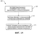
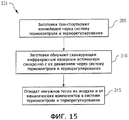
Более конкретно, изобретение относится к новому эффективному способу направления инфракрасного излучения по меньшей мере одной конкретной оптимальной длины волны на целевой объект для изменения температуры этого объекта. Отметим, что "целевыми объектами" инфракрасного облучения могут быть самые разнообразные предметы, например отдельные объекты, обрабатываемые в ходе какой-либо технологической операции, локальные зоны материала для непрерывной цикличной обработки, пища в процессе ее приготовления, люди, которым оказывается медицинская помощь, и т.д.More specifically, the invention relates to a new effective method for directing infrared radiation of at least one specific optimal wavelength to a target object to change the temperature of this object. Note that the "target" of infrared irradiation can be a wide variety of objects, for example, individual objects processed during any technological operation, local zones of material for continuous cyclic processing, food during its preparation, people who receive medical care, and etc.
Хотя данное изобретение описано ниже на примере нагрева заготовок для пластиковых бутылок, его принципы в равной степени применимы и в отношении других упомянутых задач. Описанный пример изобретения относится к одноэтапным операциям выдувания пластиковых бутылок, когда предварительно выполняют операцию литьевого формования (как раз перед операцией выдувного формования). В данном виде применения изобретения, предложенные способы и устройство обеспечивают по сути те же преимущества, что и известные технические решения, однако они используют другие средства измерения и управления, позволяющие учитывать различия в начальной температуре на входе в секцию нагрева.Although the invention is described below by the example of heating blanks for plastic bottles, its principles are equally applicable to the other problems mentioned. The described example of the invention relates to one-step operations of blowing plastic bottles when the injection molding operation is performed previously (just before the blow molding operation). In this type of application of the invention, the proposed methods and device provide essentially the same advantages as the known technical solutions, however, they use other means of measurement and control, allowing to take into account differences in the initial temperature at the inlet to the heating section.
В идеальном случае система инфракрасного нагрева оптимально нагревает целевой объект при наименьшем потреблении энергии. Такая система может содержать устройство, преобразующее подводимую электрическую энергию непосредственно в энергию электромагнитного облучения с единственной выбранной длиной волны или с группой волн узкого диапазона, направленную на целевой объект, в результате чего энергия излучения будет частично или полностью поглощаться целевым объектом, преобразовываясь в тепло. Чем эффективнее входная электроэнергия преобразуется в электромагнитное излучение, тем эффективнее действует система. Чем точнее излученные электромагнитные волны нацелены на выбранные участки целевого объекта, тем эффективнее система выполняет свою функцию. Излучающее устройство, выбранное для использования, должно обладать свойством мгновенного включения и мгновенного выключения, чтобы ни входная, ни выходная энергия не тратились напрасно, когда целевой объект не облучается. Чем эффективнее облучаемый целевой объект поглощает излученную электромагнитную энергию, преобразуя ее в тепло, тем эффективнее функционирует система. Для оптимизации работы системы необходимо, чтобы набор длин волн ее выходного излучения соответствовал поглощающим характеристикам целевого объекта. Эти длины волн, очевидно, должны по-разному выбираться для разных задач изобретения, чтобы как можно точнее соответствовать различным поглощающим характеристикам различных материалов, а также обеспечивать различные желательные результаты.In the ideal case, the infrared heating system optimally heats the target with the least energy consumption. Such a system may include a device that converts the supplied electric energy directly into electromagnetic radiation energy with a single selected wavelength or with a group of narrow-band waves directed at the target object, as a result of which the radiation energy will be partially or completely absorbed by the target object, converted into heat. The more efficient the input electricity is converted to electromagnetic radiation, the more efficient the system. The more accurately the emitted electromagnetic waves are aimed at selected areas of the target object, the more efficiently the system performs its function. The emitting device selected for use must have the ability to instantly turn on and turn off instantly so that neither input nor output energy is wasted when the target is not irradiated. The more effectively the irradiated target absorbs the radiated electromagnetic energy, converting it into heat, the more efficient the system functions. To optimize the operation of the system, it is necessary that the set of wavelengths of its output radiation corresponds to the absorbing characteristics of the target object. These wavelengths, obviously, should be chosen differently for different tasks of the invention in order to match the various absorbing characteristics of different materials as accurately as possible, as well as provide different desired results.
Из уровня техники хорошо известно использование излучающих нагревательных систем различного типа, предназначенных для проведения самых разных обработок и лечебных процедур. Технологии, которые были разработаны ранее для таких целей, обеспечивают достаточно широкий диапазон частот излучаемой электромагнитной энергии. Несмотря на то, что эти системы могут упоминаться в данной области техники как системы лечения или обработки посредством инфракрасного нагрева, на самом деле они зачастую производят лучевую энергию далеко за пределами инфракрасного спектра.The use of radiating heating systems of various types is well known in the prior art for a wide variety of treatments and treatment procedures. Technologies that were previously developed for such purposes provide a fairly wide range of frequencies of radiated electromagnetic energy. Although these systems may be referred to in the art as infrared heating treatment or treatment systems, in fact they often produce radiation energy far beyond the infrared spectrum.
Инфракрасная часть спектра делится по длинам волн на три основные области: область коротких волн, область средних волн и область длинных волн инфракрасных лучей. Точные границы между этими основными областями ясно не установлены, однако считается, что область коротких волн инфракрасных лучей охватывает диапазон от верхнего предела визуальной способности человеческого глаза (примерно 780 нм) и до 1,5 мкм. Область средних волн инфракрасных лучей охватывает диапазон от 1,5 до 5 мкм. Область длинных волн инфракрасных лучей, как принято считать, лежит между 5 мкм и 14 мкм и даже простирается дальше. Вообще предполагается, что реальное тепловое инфракрасное излучение включает в себя диапазоны средних, длинных и сверхдлинных волн. Инфракрасное излучение области коротких волн, напротив, ведет себя подобно невидимому свету.The infrared part of the spectrum is divided according to wavelengths into three main areas: the region of short waves, the region of medium waves and the region of long waves of infrared rays. The exact boundaries between these main areas are not clearly established, however, it is believed that the region of short waves of infrared rays covers the range from the upper limit of the visual ability of the human eye (approximately 780 nm) to 1.5 microns. The medium wavelength range of infrared rays covers a range of 1.5 to 5 microns. The region of long waves of infrared rays, as is commonly believed, lies between 5 μm and 14 μm and even extends further. It is generally assumed that real thermal infrared radiation includes ranges of medium, long and extra-long waves. In contrast, the infrared radiation of the shortwave region behaves like an invisible light.
Известные источники инфракрасного излучения, используемые в промышленном, коммерческом и медицинском нагревательном оборудовании для лечебных или технологических процессов, генерируют электромагнитные волны в широком диапазоне частот, редко ограниченном только одной областью инфракрасного спектра. Хотя выходная мощность таких широкополосных установок может достигать максимума в конкретном диапазоне инфракрасного спектра, у них обычно присутствуют побочные пики, которые простираются далеко в смежные частотные области.Known infrared sources used in industrial, commercial and medical heating equipment for medical or technological processes generate electromagnetic waves in a wide frequency range, rarely limited to only one region of the infrared spectrum. Although the output power of such broadband installations can reach a maximum in a particular infrared range, they usually have side peaks that extend far into adjacent frequency domains.
Например, известные из уровня техники кварцевые лампы инфракрасного нагрева, используемые для операций нагрева в различных процессах, обычно обеспечивают пиковую мощность в диапазоне от 0,8 до 1 мкм. Хотя их мощность достигает своего максимума в диапазоне 0,8 и 1 мкм, эти лампы также излучают значительную энергию в широком непрерывном диапазоне волн, начиная от ультрафиолетового излучения (УФ), продолжая видимым диапазоном и доходя примерно до 3,5 мкм в средневолновой области инфракрасных лучей. Понятно, что несмотря на то, что пиковая мощность кварцевой лампы приходится на область коротких волн инфракрасных лучей, лампа излучает значительную мощность и в видимой, и в средневолновой областях инфракрасных лучей. Вследствие этого существующие широкодиапазонные источники инфракрасного излучения не способны обеспечить избирательное излучение на какой-либо предпочтительной длине волны или длинах волн, которые были бы наиболее подходящими для конкретной задачи нагрева, обработки или лечения. В сущности, эти процессы представляют собой лечение или обработку электромагнитным излучением широкодиапазонного спектра. До появления настоящего изобретения они широко использовались лишь по причине отсутствия других альтернатив, за исключением альтернатив, описанных в совместно рассматриваемых заявках №11/003679 (подана 3 декабря 2004) и №011/351030 (подана 9 февраля 2006), содержание которых включено в данную заявку посредством ссылки. Основное повышение температуры у многих целевых объектов происходит из-за поглощения ими тепловой энергии инфракрасного излучения, характеризующейся узким диапазоном волн, одним или несколькими. Таким образом, большая часть энергии инфракрасного излучения, распределенной в широком диапазоне, тратится впустую.For example, infrared quartz lamps of the prior art used for heating operations in various processes typically provide peak powers in the range of 0.8 to 1 μm. Although their power reaches its maximum in the range of 0.8 and 1 μm, these lamps also emit significant energy in a wide continuous wave range, ranging from ultraviolet radiation (UV), continuing the visible range and reaching approximately 3.5 μm in the mid-wave infrared region rays. It is clear that despite the fact that the peak power of a quartz lamp falls on the region of short waves of infrared rays, the lamp emits significant power in both the visible and medium-wave regions of infrared rays. As a result, existing wide-range infrared sources are not capable of providing selective radiation at any preferred wavelength or wavelengths that would be most suitable for a particular heating, processing or treatment task. In essence, these processes are treatment or treatment with electromagnetic radiation of a wide-range spectrum. Prior to the invention, they were widely used only because of the absence of other alternatives, with the exception of the alternatives described in the jointly pending applications No. 11/003679 (filed December 3, 2004) and No. 011/351030 (filed February 9, 2006), the contents of which are included in this application by reference. The main temperature increase in many target objects is due to their absorption of the thermal energy of infrared radiation, characterized by a narrow wavelength range, one or more. Thus, most of the energy of infrared radiation, distributed over a wide range, is wasted.
Тем не менее, кварцевые инфракрасные лампы широко используются в промышленности как для дискретной, так и для непрерывной обработки материалов. Чтобы направить излучение кварцевой лампы на целевой объект, в технологическом процессе обычно используют различные средства, включающие отражатели разных типов. Независимо от того, каким образом энергия фокусируется на целевом объекте, кварцевые лампы обычно запитываются электропитанием непрерывно. Это относится к случаям когда целевой объект является и непрерывно облучаемым, и дискретно. Причина этого прежде всего заключается в том, что тепловые кварцевые лампы достаточно медленные и им свойственно продолжительное время реагирования, составляющее обычно несколько секунд. Кварцевые лампы представляют собой "медленные" устройства как в отношении включения, так и в отношении выключения, и потому фактически не могут эффективно быстро включаться и быстро выключаться или работать синхронно импульсам малой длительности.Nevertheless, quartz infrared lamps are widely used in industry for both discrete and continuous processing of materials. To direct the radiation of a quartz lamp to a target object, various means are usually used in the technological process, including reflectors of various types. Regardless of how the energy is focused on the target, quartz lamps are usually powered continuously. This applies to cases where the target is both continuously irradiated and discrete. The reason for this, first of all, is that thermal quartz lamps are rather slow and have a long reaction time, usually a few seconds. Quartz lamps are “slow” devices both with respect to switching on and turning off, and therefore, in fact, they cannot effectively turn on and off quickly or work synchronously with short-duration pulses.
В качестве примера области применения предложенного способа направления энергии можно указать область формования раздувом. В частности, в системах формования пластиковых бутылок раздувом с вытяжкой, специальные температурные условия необходимо создавать предварительно, т.е. перед проведением операций формования раздувом с вытяжкой. Один аспект этого процесса известен из уровня техники как операция подогрева. В операции подогрева заготовки, образованные в ходе теплового литьевого формования или в ходе компрессионного формования, охлаждают до температуры окружающей среды или до комнатной температуры и стабилизируют при этой температуре. Некоторое время спустя, которое обычно составляет несколько дней или недель, заготовки подают в систему формования раздувом с вытяжкой, в которой на начальной стадии обработки заготовки нагревают до некоторой температуры, причем определенную часть термопластического материала заготовки нагревают до температуры, оптимизированной для последующих операций формования раздувом. Выполнение этого условия обеспечивают во время транспортировки заготовок через секцию нагрева или печь, предусмотренные на пути транспортировки к секции формования раздувом в установке. В секции формования раздувом заготовки сначала механически растягивают и затем раздувают (обычно воздухом повышенного давления) до формы сосудов или контейнеров большего объема. Примером такого контейнера является одноразовая бутылка для воды или газированного напитка, изготовленная из материала ПЭТ (полиэтилентерефталат).As an example of the scope of the proposed method of directing energy, you can specify the area of blow molding. In particular, in blow molding systems for plastic bottles with a hood, special temperature conditions must be created in advance, i.e. before carrying out blow molding operations. One aspect of this process is known in the art as a preheating operation. In the heating operation, the preforms formed during thermal injection molding or during compression molding are cooled to ambient temperature or to room temperature and stabilized at this temperature. Some time later, which is usually several days or weeks, the preforms are fed into an extrusion blow molding system in which at the initial stage of processing the preforms are heated to a certain temperature, and a certain part of the thermoplastic material of the preform is heated to a temperature optimized for subsequent blow molding operations. The fulfillment of this condition is ensured during the transportation of the workpieces through the heating section or furnace provided on the transportation path to the blow molding section in the installation. In the blow-molding section, the preforms are first mechanically stretched and then inflated (usually with high pressure air) to form larger vessels or containers. An example of such a container is a disposable bottle for water or a carbonated drink made from PET (polyethylene terephthalate) material.
Затраты энергопотребления существенно влияют на стоимость готовой продукции, создаваемой формованием раздувом, и обычно являются самыми высокими издержками производства. В частности, количество энергии, используемое при известном способе нагрева заготовки из терефталата полиэтилена (ПЭТ) от температуры окружающей среды до 105°С в секции нагрева, входящей в состав установки формования раздувом с вытяжкой, является крайне существенным. Что касается остальных аспектов повышения эффективности производства, то с экономической и экологической точек зрения необходимо уменьшать энергопотребление, связанное с функционированием секции поддержания температурных условий в системах формования раздувом с вытяжкой.Energy costs significantly affect the cost of finished products created by blow molding, and are usually the highest production costs. In particular, the amount of energy used in the known method of heating a preform of polyethylene terephthalate (PET) from an ambient temperature of up to 105 ° C in a heating section included in a blow molding molding machine is extremely significant. As for the other aspects of increasing production efficiency, from an economic and environmental point of view it is necessary to reduce the energy consumption associated with the functioning of the section for maintaining temperature conditions in blow molding systems with hoods.
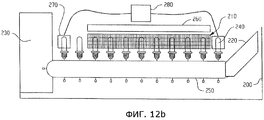
Кроме того, согласно современной практике контейнеры подвергают действию энергии, излучаемой группой кварцевых инфракрасных ламп типа W-VII, образующих туннельную печь. Энергия каждой лампы имеет разброс в широких пределах, вследствие чего степень облучения отдельных сегментов контейнера можно регулировать очень незначительно. Большая часть энергии ламп вообще не поглощается контейнером, а поглощается окружающим воздухом и механическими опорами, что приводит к значительному снижению общей эффективности. Для снижения нежелательного нагрева можно предпринимать некоторые меры, например, туннельную печь обдувают воздухом с целью 1) охлаждения внешней оболочки контейнера (что очень желательно) и 2) направления в контейнеры больше энергии за счет конвекции излишне нагретого воздуха.In addition, according to modern practice, containers are exposed to energy emitted by a group of quartz infrared lamps of type W-VII, forming a tunnel furnace. The energy of each lamp has a wide range, as a result of which the degree of irradiation of individual segments of the container can be regulated very slightly. Most of the lamp energy is not absorbed at all by the container, but is absorbed by the surrounding air and mechanical supports, which leads to a significant decrease in overall efficiency. Some measures can be taken to reduce unwanted heating, for example, a tunnel kiln is blown with air in order to 1) cool the outer shell of the container (which is very desirable) and 2) direct more energy into the containers due to convection of excessively heated air.
К недостаткам способа, известного из уровня техники, относятся ненужный нагрев воздуха и смежных конструкций, плохая регулируемость распределения по контейнеру энергии облучения, необходимость использования больших физических пространств, неспособность выборочно нагревать конкретные участки или области заготовок, низкая способность быстрой адаптации распределения нагрева к новым технологическим требованиям, таким как частая смена типов контейнеров с различными размерами, и вытекающие отсюда проблемы. Например, из-за того лучевая энергия поглощается контейнерной заготовкой не полностью, приходится повышать мощность туннельной печи, задействовать дополнительные ресурсы на снижение избыточной высокой температуры среды в установке, использовать больше пространства в туннельной печи для обеспечения постепенного и однородного нагрева, чаще менять сгоревшие и частично утратившие излучающую способность лампы.The disadvantages of the method known from the prior art include unnecessary heating of air and adjacent structures, poor controllability of the distribution of irradiation energy over the container, the need to use large physical spaces, the inability to selectively heat specific sections or areas of workpieces, low ability to quickly adapt the heat distribution to new technological requirements , such as frequent changes in container types with different sizes, and the resulting problems. For example, because of this, radiation energy is not completely absorbed by the container blank, it is necessary to increase the capacity of the tunnel kiln, use additional resources to reduce the excess high temperature of the environment in the installation, use more space in the tunnel kiln to ensure gradual and uniform heating, often change burned and partially lost the emissivity of the lamp.
В патенте США №5322651 раскрыт улучшенный способ тепловой обработки термопластичных заготовок. В этом патенте описана обычная практика использования широкополосного инфракрасного (ИК) лучевого нагрева для тепловой обработки пластичных заготовок. Приведем цитату из этого патента: "По сравнению с другими нагревающими или тепловыми способами обработки, такими как конвекция и проводимость, нагрев с использованием инфракрасного облучения обеспечивает более высокую производительность и позволяет улучшить нормы изготовления, тем более принимая во внимание низкую удельную теплопроводность материала". Этот патент описывает широкополосные источники инфракрасного облучения, которые сегодня обычно используют в промышленности для обработки изделий из материала ПЭТ.US Pat. No. 5,322,651 discloses an improved method for heat treating thermoplastic preforms. This patent describes the common practice of using broadband infrared (IR) beam heating to heat plastic workpieces. We quote from this patent: "Compared to other heating or thermal processing methods, such as convection and conductivity, heating using infrared radiation provides higher productivity and improves manufacturing standards, especially taking into account the low thermal conductivity of the material." This patent describes broadband infrared sources that are commonly used today in industry for processing PET products.
Конкретное усовершенствование известных способов, предложенное в данном патенте, относится к управлению избыточной энергией, излучаемой во время ИК-нагрева заготовок. В частности, данный патент касается энергии, излучаемой во время процесса нагрева, которая в конечном счете (за счет поглощения другими элементами, отличными от заготовок, проводимости и последующей конвекции) приводит к увеличению температуры воздуха, окружающего транспортируемые по печи заготовки. Конвекционный нагрев заготовок, обусловленный струей горячего воздуха, как выяснилось, приводит к неоднородному нагреву заготовок и, таким образом, вредно сказывается на технологическом процессе. Бесполезный расход энергии также присущ установке системы HVAC, которая тоже отличается большим энергопотреблением. Патент №5322651 описывает способ, противодействующий влиянию непреднамеренного нагрева воздуха, окружающего заготовки во время операций ИК-нагрева.A specific improvement of the known methods proposed in this patent relates to the control of excess energy emitted during infrared heating of the workpieces. In particular, this patent relates to energy emitted during the heating process, which ultimately (due to absorption by elements other than blanks, conductivity and subsequent convection) leads to an increase in air temperature surrounding the blanks transported through the furnace. Convection heating of the workpieces caused by a jet of hot air, as it turned out, leads to inhomogeneous heating of the workpieces and, thus, adversely affects the process. Useless energy consumption is also inherent in the installation of the HVAC system, which is also characterized by high energy consumption. Patent No. 5322651 describes a method that counteracts the influence of unintentional heating of the air surrounding the workpiece during infrared heating operations.
Таким образом понятно, что передача тепловой энергии от известных современных широкополосных элементов и систем ИК-нагрева к обрабатываемым заготовкам является недостаточно эффективной. В идеальном случае выбранные участки заготовок должны поглощать в виде тепловой энергии все 100% энергии, предназначенной для тепловой обработки этих заготовок. Хотя это специально не оговорено в перечисленных выше патентах, типичные значения эффективности передачи энергии (отношение: энергия, полученная транспортируемыми заготовками/энергия, потребленная ИК-нагревателями) у известных установок формования раздувом лежат в пределах 5%-10%. Несмотря на то, что это трудно проверить на практике, но фактическая эффективность передачи энергии у этих систем вряд ли достигает даже такого уровня. Поэтому любое усовершенствование способов или средств, связанных с инфракрасным нагревом заготовок, повышающее эффективность передачи энергии, является чрезвычайно предпочтительным и обуславливает существенное снижение энергозатрат при использовании установок формования раздувом с вытяжкой.Thus, it is clear that the transfer of thermal energy from known modern broadband elements and IR heating systems to workpieces is not effective enough. In the ideal case, the selected sections of the workpieces should absorb in the form of heat energy all 100% of the energy intended for the heat treatment of these workpieces. Although not specifically mentioned in the patents listed above, typical values of energy transfer efficiency (ratio: energy received by transported blanks / energy consumed by infrared heaters) in known blow molding machines are within 5% -10%. Although this is difficult to verify in practice, the actual energy transfer efficiency of these systems is unlikely to even reach that level. Therefore, any improvement in the methods or means associated with infrared heating of workpieces, increasing the efficiency of energy transfer, is extremely preferable and leads to a significant reduction in energy consumption when using blow molding molding machines.
Есть много факторов, которые способствуют повышению эффективности передачи энергии элементов и систем ИК-нагрева, используемых в известных установках формования раздувом. Как замечено выше, стандартные термопластичные заготовки, такие как заготовки из материала ПЭТ, нагревают примерно до температуры 105°С. Обычно это осуществляют в известных установках формования раздувом с использованием коммерчески доступных широкополосных кварцевых инфракрасных ламп. В быстродействующих / высокопроизводительных установках эти лампы зачастую образуют большие группы баллонов очень высокой мощности. Общая энергия, потребляемая всеми группами кварцевых ламп, обуславливает огромное токопотребление, которое в самых быстрых установках выливается во многие сотни киловатт потребляемой мощности. Два фактора, связанные с элементами ИК-нагрева этого типа и оказывающие влияние на эффективность передачи общей энергии всей нагревательной системы, - это цветовая температура нити лампы и свойства оптической передачи баллона лампы.There are many factors that contribute to improving the energy transfer efficiency of elements and infrared heating systems used in known blow molding machines. As noted above, standard thermoplastic preforms, such as preforms of PET material, are heated to approximately 105 ° C. This is usually carried out in known blow molding machines using commercially available broadband quartz infrared lamps. In high-speed / high-performance installations, these lamps often form large groups of cylinders of very high power. The total energy consumed by all groups of quartz lamps causes a huge current consumption, which in the fastest installations is poured into many hundreds of kilowatts of power consumption. Two factors associated with infrared heating elements of this type and affecting the transmission efficiency of the total energy of the entire heating system are the color temperature of the lamp filament and the optical transmission properties of the lamp bulb.
Другим фактором, оказывающим существенное влияние на эффективность передачи общей энергии тепловых подсистем, используемых в известных установках формования раздувом, является управление потоком или средствами фокусировки, предназначенными для направления ИК-излучения, испускаемого нагревательными элементами, в заготовки, транспортируемые через эту систему. В большинстве известных установок формования раздувом используются специальные средства, обеспечивающие направление потока ИК-лучей, испускаемых кварцевыми лампами, непосредственно на заготовки. В частности, используются металлизированные отражатели, позволяющие значительно снизить количество испускаемого ИК-излучения, которое в этих системах расходуется впустую.Another factor that has a significant impact on the transfer efficiency of the total energy of the thermal subsystems used in known blow molding machines is the control of the flow or focusing means designed to direct the infrared radiation emitted by the heating elements into the workpieces transported through this system. In most known blow molding machines, special tools are used to direct the flow of infrared rays emitted by quartz lamps directly to the workpieces. In particular, metallized reflectors are used to significantly reduce the amount of emitted infrared radiation that is wasted in these systems.
Еще одним фактором, влияющим на эффективность передачи энергии в подсистемах ИК-нагрева, является степень синхронизации энергии, подводимой к стационарным элементам ИК-нагрева, с движением заготовок, перемещаемых через нагревательную систему. Более конкретно, если входная энергия непрерывно потребляется стационарным элементом ИК-нагрева в фиксированном количестве, даже в то время, когда в непосредственной близости от нагревателя нет ни одной заготовки по причине непрерывного движения заготовок через систему, то очевидно, что эффективность передачи энергии в этой системе не оптимизирована. На практике, медленное физическое срабатывание коммерчески доступных кварцевых ламп и относительно высокие скорости транспортировки заготовок в известных установках формования раздувом нивелируют любую успешную попытку модуляции входной мощности лампы с целью синхронизации ее облучения с дискретным движением компонента и, таким образом, не позволяют повысить эффективность передачи общей энергии.Another factor affecting the efficiency of energy transfer in the infrared heating subsystems is the degree of synchronization of energy supplied to the stationary infrared heating elements with the movement of the workpieces moved through the heating system. More specifically, if the input energy is continuously consumed by a stationary infrared heating element in a fixed amount, even when there is not a single workpiece in the immediate vicinity of the heater due to the continuous movement of the workpieces through the system, it is obvious that the energy transfer efficiency in this system not optimized. In practice, the slow physical actuation of commercially available quartz lamps and the relatively high speed of transportation of workpieces in known blow molding machines neutralize any successful attempt to modulate the lamp input power in order to synchronize its irradiation with the discrete movement of the component and, thus, do not allow to increase the overall energy transfer efficiency .
В американских патентах №5925710, 6022920 и 6503586 раскрыты подобные способы увеличения доли энергии, испускаемой ИК-лампами, которая поглощается заготовками, транспортируемыми в процессе формования раздувом. Все эти патенты описывают, с разной степенью детализации, общую практику нагрева в известных установках формования раздувом с использованием кварцевых ламп в качестве элементов ИК-нагрева. Согласно процессу теплового формования раздувом заготовки, которые ранее были созданы методом литьевого формования и доведены до комнатной температуры, нагревают до нужной температуры лишь непосредственно перед операцией формования раздувом. Вышеупомянутые патенты описывают, как полимеры вообще и ПЭТ, в частности, могут быть нагреты поглощением ИК-излучения более эффективно, чем это возможно с использованием проводимости или конвекционных средств. В этих патентах измеренный коэффициент поглощения материала ПЭТ графически представлен в виде функции длины волны. Для материала ПЭТ обнаружен ряд диапазонов с большим молекулярным поглощением, прежде всего в ИК-диапазонах для длин волн больше 1,6 мкм. Кварцевые лампы, как известно, излучают в широком спектре, и точный спектр излучения может быть определен по температуре нити накала в соответствии с законом Планка.In US patents No. 5925710, 6022920 and 6503586 disclosed similar ways to increase the proportion of energy emitted by infrared lamps, which is absorbed by the workpieces transported during blow molding. All these patents describe, with varying degrees of detail, the general practice of heating in known blow molding machines using quartz lamps as IR heating elements. According to the process of thermal blow molding, preforms that were previously created by injection molding and brought to room temperature are heated to the desired temperature only immediately before the blow molding operation. The aforementioned patents describe how polymers in general and PET in particular can be heated by absorption of infrared radiation more efficiently than is possible using conductivity or convection means. In these patents, the measured absorption coefficient of the PET material is graphically represented as a function of wavelength. A number of ranges with high molecular absorption were found for the PET material, primarily in the IR ranges for wavelengths greater than 1.6 μm. Quartz lamps are known to emit a wide spectrum, and the exact spectrum of radiation can be determined by the temperature of the filament in accordance with Planck's law.
Кварцевые лампы, используемые в известных установках формования раздувом, работают при температуре нити накала около 3000 К. При этой температуре пик излучения ламп приходится на длину волны примерно 0,8 мкм. Поскольку эмиссией, согласно данной области техники, принято считать эмиссию абсолютно черного тела, то можно сказать, что нить кварцевой лампы излучает непрерывный спектр энергии от рентгеновского излучения до сверхдлинноволнового инфракрасного излучения. При цветовой температуре 3000 К эмиссия растет по всей видимой области спектра, достигает максимума на длине волны 0,8 мкм и затем постепенно уменьшается, поскольку она начинает попадать в область значительного поглощения материала ПЭТ, которая начинается с длины волны примерно 1,6 мкм.The quartz lamps used in known blow molding machines operate at a filament temperature of about 3000 K. At this temperature, the peak radiation of the lamps falls at a wavelength of about 0.8 microns. Since emission, according to this technical field, is considered to be absolutely black body emission, it can be said that a quartz lamp filament emits a continuous energy spectrum from x-ray radiation to ultra-long-wave infrared radiation. At a color temperature of 3000 K, emission increases over the entire visible region of the spectrum, reaches a maximum at a wavelength of 0.8 μm, and then gradually decreases, since it begins to fall into the region of significant absorption of PET material, which begins with a wavelength of about 1.6 μm.
Но ни в одном из этих патентов не описано влияние кварцевого баллона на спектр излучения лампы. У кварцевого материала, используемого при изготовлении баллонов для коммерческих кварцевых ламп, есть верхний предел передачи, соответствующий длине волны примерно 3,5 мкм. За пределами этой длины волны любая энергия, излучаемая помещенной в баллон нитью, большей частью поглощается кварцевым стеклом баллона, в котором размещена нить накаливания, и поэтому непосредственно не может быть использована для нагрева заготовки.But none of these patents describes the effect of a quartz balloon on the emission spectrum of a lamp. The quartz material used in the manufacture of cylinders for commercial quartz lamps has an upper transmission limit corresponding to a wavelength of about 3.5 microns. Outside of this wavelength, any energy radiated by the filament placed in the cylinder is mostly absorbed by the quartz glass of the cylinder in which the filament is located, and therefore cannot directly be used to heat the workpiece.
В силу указанных выше причин в известных установках формования раздувом, в которых для нагрева заготовки из материала ПЭТ до температуры раздува используются кварцевые лампы, диапазон нагрева поглощением расположен между 1 мкм и 3,5 мкм. Все вышеупомянутые патенты (№№5925710, 6022920 и 6503586) описывают различные способы и средства, предназначенные для изменения естественных поглощающих свойств заготовки, а значит для улучшения эффективности преобразования общей энергии в процессе нагрева. Все эти патенты раскрывают добавление в материал ПЭТ заготовки инородных материалов, осуществляемое с единственной целью увеличения коэффициента поглощения смеси материалов. Эти описанные способы и средства направлены на изменение оптических поглощающих свойств материала в диапазоне от ближней области ИК-излучения, примерно 0,8 мкм, до 3,5 мкм. Указанное изменение поглощающих свойств заготовок действительно позволяет повысить эффективность преобразования общей энергии в процессе нагрева и обеспечивает снижение затрат на изготовление контейнера. Однако оно, к сожалению, также связано с ухудшением внешнего вида готового контейнера. Снижение оптической прозрачности контейнера, иногда называемое замутнением контейнера, заставляет считать этот подход неоптимальным решением поставленной технологической задачи.Due to the above reasons, in known blow molding machines in which quartz lamps are used to heat a preform of PET material to a blow temperature, the absorption heating range is between 1 μm and 3.5 μm. All the aforementioned patents (Nos. 5925710, 6022920 and 6503586) describe various methods and means for changing the natural absorbing properties of a workpiece, and therefore for improving the efficiency of the conversion of total energy during heating. All these patents disclose the addition of foreign material preforms to the PET material, carried out for the sole purpose of increasing the absorption coefficient of the mixture of materials. These described methods and means are aimed at changing the optical absorbing properties of the material in the range from the near infrared region, about 0.8 microns, to 3.5 microns. The specified change in the absorbing properties of the workpieces really allows you to increase the efficiency of the conversion of the total energy during heating and reduces the cost of manufacturing the container. However, it, unfortunately, is also associated with a deterioration in the appearance of the finished container. The decrease in the optical transparency of the container, sometimes called the clouding of the container, makes us consider this approach as an optimal solution to the assigned technological problem.
Патент США №5206039 описывает одностадийную систему формования литьем/раздувом, включающую в себя улучшенное средство кондиционирования заготовок и их транспортировки от зоны литья до зоны раздува. Согласно этому патенту автономная работа установки формования литьем и установки формования раздувом, при которой каждая из них добавляет значительное количество энергии в процесс температурного кондиционирования термопластичного материала, оценена как расточительная. В этом патенте утверждается, что одноэтапный производственный процесс позволяет сократить как потребление общей энергии, так и производственные затраты. Это сокращение потребления энергии обусловлено прежде всего тем, что большая часть тепловой энергии, необходимой для проведения операции формования раздувом, уже содержится в заготовке после этапа литьевого формования. Более конкретно, согласно одноэтапному процессу, описанному в патенте №5206039, заготовку не охлаждают до комнатной температуры после литьевого формования. Напротив, с этапа литьевого формования заготовки перемещают без задержки непосредственно в секцию теплового кондиционирования и затем в секцию формования раздувом.US Patent No. 5,206,039 describes a one-step injection / blow molding system that includes an improved means of conditioning the workpieces and transporting them from the cast zone to the blow zone. According to this patent, the autonomous operation of the injection molding unit and the blow molding installation, in which each of them adds a significant amount of energy to the temperature conditioning process of the thermoplastic material, is rated wasteful. This patent claims that a one-stage production process reduces both total energy consumption and production costs. This reduction in energy consumption is primarily due to the fact that most of the thermal energy needed for the blow molding operation is already contained in the workpiece after the injection molding step. More specifically, according to the one-step process described in patent No. 5206039, the preform is not cooled to room temperature after injection molding. In contrast, from the injection molding step, the preforms are transferred without delay directly to the thermal conditioning section and then to the blow molding section.
В секции теплового кондиционирования, описанной в патенте №5206039, созданы условия как для добавления небольшого количество тепловой энергии, так и выдержки заготовок для стабилизации в течение регулируемого периода времени. Это отличается от требований секции теплового кондиционирования для 2-этапного процесса в установке горячего формования раздувом, в которой для разогрева заготовки до температуры раздува необходимо большое количество энергии. Хотя использование одноэтапных установок формования литьем/раздувом известно из уровня техники, проблемы качества готовых контейнеров, выпускаемых этими установками, остаются прежними. Эти проблемы качества связаны с изменением температуры от заготовки к заготовке, по мере того как поток заготовок поступает в зону раздува. Несмотря на достижения, описанные в патенте №5206039, основанные на использовании известных средств и способов ИК-нагрева и измерения температуры, процесс теплового кондиционирования заготовок сразу после их удаления с этапа литьевого формования тем не менее все еще приводит к разнице содержания тепла в заготовках, поступающих в зону раздува. Разница в содержании тепла поступающих заготовок приводит к разнице свойств и качества готовых контейнеров. Невозможность эффективно отрегулировать процесс ИК-нагрева для устранения разницы в качестве между заготовками заставляет изготовителей обратиться к использованию способа формования раздувом с повторным нагревом с целью достижения необходимого уровня качества. Поэтому, что касается самых высокопроизводительных применений, то изготовители по-прежнему придерживаются в этих случаях способов формования с повторным нагревом. Кроме того, процесс повторного нагрева по-прежнему остается популярным и с той точки зрения, что предприятия-изготовители зачастую продают конечному пользователю изделия в виде заготовок, а тот впоследствии сам выдувает из них контейнеры и заполняет эти контейнеры.In the thermal conditioning section described in patent No. 5206039, conditions have been created for both adding a small amount of thermal energy and holding the workpieces for stabilization for an adjustable period of time. This differs from the requirements of the thermal conditioning section for a 2-stage process in a hot blow molding plant, in which a large amount of energy is required to heat the workpiece to a blow temperature. Although the use of one-stage injection molding machines is known from the prior art, the quality problems of finished containers produced by these installations remain the same. These quality problems are associated with a change in temperature from the workpiece to the workpiece as the workpiece stream enters the inflation zone. Despite the achievements described in patent No. 5206039, based on the use of known means and methods of IR heating and temperature measurement, the process of thermal conditioning of workpieces immediately after they are removed from the injection molding stage nevertheless still leads to a difference in the heat content in the workpieces coming into the inflation zone. The difference in the heat content of the incoming billets leads to a difference in the properties and quality of the finished containers. The inability to effectively adjust the IR heating process to eliminate the difference in quality between the blanks makes manufacturers turn to the use of blow molding with reheating in order to achieve the required level of quality. Therefore, for the most high-performance applications, manufacturers still adhere to reheating molding methods in these cases. In addition, the reheating process is still popular from the point of view that manufacturers often sell products to the end user in the form of blanks, and he subsequently blows containers out of them and fills these containers.
Перспектива улучшения эффективности и/или функциональных возможностей секции ИК-нагрева в установках формования раздувом несомненно предпочтительна как в отношении эксплуатационных расходов, так и в отношении качества продукции. Хотя были предприняты некоторые попытки добиться усовершенствования известных подсистем ИК-нагрева, очевидно, что некоторые их недостатки все еще не исправлены. Таким образом, задача настоящего изобретения заключается в преодолении указанных недостатков за счет создания новых принципов и способов ИК-нагрева.The prospect of improving the efficiency and / or functionality of the infrared heating section in blow molding machines is undoubtedly preferable both in terms of operating costs and product quality. Although some attempts have been made to improve the known infrared heating subsystems, it is obvious that some of their shortcomings are still not fixed. Thus, the objective of the present invention is to overcome these disadvantages by creating new principles and methods of infrared heating.
В области твердотельной электроники хорошо известны когерентные твердотельные излучатели или лазерные диоды. Фотонные или потоковые излучатели этого типа коммерчески доступны и работают на различных частотах от ультрафиолетового облучения (УФ) до ближней области инфракрасного спектра. Светодиоды построены на основе соответствующих полупроводниковых материалов n-типа и р-типа. Некоторое количество полупроводникового материала, содержащего после соответствующей обработки легированную область с акцепторной примесью (р-типа), введенное в прямой контакт с некоторым количеством того же материала, содержащего область, легированную донорной примесью (n-типа), называется диодом. Как известно из данной области техники, диоды обладают рядом важных электрических и фотоэлектрических свойств. Например, известно, что в физической области раздела между областью с донорной примесью (n-типа) и областью с акцепторной примесью (р-типа), собственно и образующей полупроводниковый диод, в материале существует характерная запрещенная энергетическая зона. Эта запрещенная энергетическая зона определяет разницу между энергетическим уровнем электронов, расположенных в зоне проводимости в области n-типа, и энергетическим уровнем электронов, расположенных в более низкой области р-типа. Электроны, при протекании под действием электрического поля через pn-переход, перемещаются с энергетического уровня, допустимого для зоны проводимости в области n-типа, на более низкий энергетический уровень, допустимый для зоны проводимости в области р-типа, что приводит к испусканию фотона при каждом таком энергетическом переходе электрона. Таким образом, точное количество выделенной энергии или, альтернативно, длина волны излучаемого фотона соответствует энергии, потерянной электроном, прошедшим рп-переход.In the field of solid state electronics, coherent solid state emitters or laser diodes are well known. Photon or flux emitters of this type are commercially available and operate at various frequencies from ultraviolet radiation (UV) to the near infrared region. LEDs are based on the corresponding n-type and p-type semiconductor materials. A certain amount of semiconductor material containing, after appropriate treatment, a doped acceptor impurity region (p-type), brought into direct contact with a certain amount of the same material, containing a donor impurity-doped region (n-type), is called a diode. As is known from the art, diodes have a number of important electrical and photoelectric properties. For example, it is known that in the physical region of the interface between the region with a donor impurity (n-type) and the region with an acceptor impurity (p-type), which actually forms a semiconductor diode, a characteristic forbidden energy zone exists in the material. This forbidden energy zone determines the difference between the energy level of electrons located in the conduction band in the n-type region and the energy level of electrons located in the lower p-type region. Electrons, when flowing under the influence of an electric field through the pn junction, move from the energy level acceptable for the conduction band in the n-type region to a lower energy level acceptable for the conduction band in the p-type region, which leads to the emission of a photon when each such energy transition of an electron. Thus, the exact amount of energy released or, alternatively, the wavelength of the emitted photon corresponds to the energy lost by the electron that has passed the pn junction.
Короче говоря, лазерные диоды действуют как излучатели, преобразующие электрический ток непосредственно в фотоны. В отличие от нити накаливания или других излучателей типа абсолютно черного тела, лазерным диодам не требуется преобразовывать входную энергию в промежуточную форму тепловой энергии, чтобы испускать фотоны. Благодаря этому свойству прямого преобразования электрического тока в фотоны, лазерные диоды обладают чрезвычайно высоким быстродействием. Лазерные диоды используются в ряде применений, требующих генерации импульсов с чрезвычайно низкой скважностью в ультрафиолетовом и видимом диапазоне световых волн и/или в ближней области инфракрасного спектра.In short, laser diodes act as emitters that convert electrical current directly into photons. Unlike incandescent filaments or other emitters such as a completely black body, laser diodes do not need to convert the input energy into an intermediate form of thermal energy in order to emit photons. Due to this property of direct conversion of electric current into photons, laser diodes have extremely high speed. Laser diodes are used in a number of applications requiring the generation of pulses with extremely low duty cycle in the ultraviolet and visible light waves and / or in the near infrared region.
В отличие от источников света на основе нити накаливания лазерные диоды излучают энергию в относительно ограниченном диапазоне волн, соответствующем конкретной запрещенной энергетической зоне используемого полупроводникового материала.Unlike light sources based on incandescent filaments, laser diodes emit energy in a relatively limited wavelength range corresponding to the specific energy gap of the semiconductor material used.
Сущность изобретенияSUMMARY OF THE INVENTION
Настоящее изобретение направлено на создание устройств инфракрасного облучения, которые обладают высокой избирательностью по длине волны и позволяют использовать инфракрасное излучение для задач и технологий нового класса, не известных из уровня техники.The present invention is directed to the creation of infrared irradiation devices that have high selectivity along the wavelength and allow the use of infrared radiation for tasks and technologies of a new class, not known from the prior art.
Первый аспект настоящего изобретения заключается в создании способа формования или другого способа или системы обработки, в которых используется система ИК-нагрева, обладающая повышенной эффективностью преобразования энергии ИК-облучения.A first aspect of the present invention is to provide a molding method or other processing method or system that utilizes an infrared heating system having enhanced infrared energy conversion efficiency.
Другой аспект изобретения заключается в создании тепловой системы ИК-нагрева, у которой можно регулировать характеристику глубины проникновения ИК-излучения для конкретного обрабатываемого или выбранного материала.Another aspect of the invention is to provide a thermal infrared heating system in which the characteristic of infrared penetration depth for a particular material being processed or selected can be adjusted.
Другой аспект настоящего изобретения заключается в создании тепловой системы ИК-облучения, содержащей комбинацию RED-диодов (например, RED-диодов на основе лазера), производящих ИК-излучение в таких выбранных узких диапазонах волн, какие являются оптимальными для задач соответствующих классов.Another aspect of the present invention is to provide a thermal IR irradiation system comprising a combination of RED diodes (e.g., laser-based RED diodes) producing IR radiation in such selected narrow wavelength ranges that are optimal for tasks of the respective classes.
Другой аспект настоящего изобретения заключается в создании системы ИК-нагрева, способной действовать в импульсном режиме; причем упомянутый импульсный режим подходит для ИК-нагрева дискретно изготовляемых частей по мере их транспортировки во время производственного процесса или для синхронного отслеживания облучаемых целевых объектов.Another aspect of the present invention is to provide an infrared heating system capable of operating in a pulsed manner; wherein said pulse mode is suitable for infrared heating of discretely manufactured parts as they are transported during the manufacturing process or for synchronous tracking of irradiated targets.
Другой аспект настоящего изобретения заключается в создании системы ИК-нагрева, которую можно точно направлять или нацеливать туда, где излучаемая тепловая энергия применяется с максимальной эффективностью.Another aspect of the present invention is to provide an infrared heating system that can accurately direct or target where radiated thermal energy is used with maximum efficiency.
Другой аспект настоящего изобретения заключается в создании системы ИК-нагрева, обладающей возможностью взаимодействия с системой измерения температуры заготовок для обеспечения особых характеристик ИК-нагрева конкретной заготовки.Another aspect of the present invention is to provide an IR heating system capable of interacting with a workpiece temperature measurement system to provide specific IR heating characteristics for a particular workpiece.
Другой аспект настоящего изобретения заключается в создании элементов инфракрасного лазерного нагрева, выполненных в виде матрицы инфракрасных твердотельных лазеров, осуществляющих прямое преобразование электрического тока в излучение фотонов, или матрицы лазерных излучающих диодов (RED-диодов).Another aspect of the present invention is the creation of infrared laser heating elements made in the form of a matrix of infrared solid-state lasers that directly convert the electric current into photon emission, or a matrix of laser emitting diodes (RED diodes).
Еще одно преимущество настоящего изобретения заключается в создании системы инфракрасного облучения, выходное излучение которой по существу соответствует выбранному очень конкретному одиночному диапазону волн или группе узких диапазонов волн.Another advantage of the present invention is to provide an infrared irradiation system, the output radiation of which essentially corresponds to the selected very specific single wavelength range or a group of narrow wavelengths.
Другое преимущество настоящего изобретения заключается в обеспечении функциональных средств для формирования мощного теплового инфракрасного облучения, программируемым образом регулируемого в отношении по меньшей мере одного из следующих параметров: положение, интенсивность, длина волны, продолжительность облучения, скорость включения/выключения, направленность, частота пульсации и отслеживание продукции.Another advantage of the present invention is to provide functional means for generating powerful thermal infrared irradiation programmable in relation to at least one of the following parameters: position, intensity, wavelength, duration of irradiation, on / off speed, directivity, ripple frequency and tracking products.
Другое преимущество настоящего изобретения состоит в более высокой эффективности прохождения тепловой энергии в материал целевого объекта по сравнению с известными широкополосными источниками излучения.Another advantage of the present invention is the higher efficiency of the passage of thermal energy into the material of the target object in comparison with the known broadband radiation sources.
Другое преимущество настоящего изобретения состоит в том, что при обеспечении нагрева заготовок бутылок их можно эффективно нагревать без необходимости добавления примесей к компонентам материала целевого объекта, которые визуально ухудшают качество и увеличивают себестоимость производства.Another advantage of the present invention is that while heating the bottle preforms, they can be heated efficiently without the need for adding impurities to the components of the target material, which visually impair the quality and increase production costs.
Другой аспект настоящего изобретения заключается в создании универсальной излучающей системы нагрева, предназначенной для задач разного класса и позволяющей расширить возможности инфракрасного облучения, отличающегося частотной избирательностью, в сочетании с программируемостью и возможностью действовать в импульсном режиме.Another aspect of the present invention is to create a universal radiating heating system designed for tasks of different classes and allowing to expand the possibilities of infrared radiation, characterized by frequency selectivity, in combination with programmability and the ability to operate in a pulsed mode.
Другое преимущество настоящего изобретения состоит в том, что оно облегчает отвод нелучистой тепловой энергии в то место, где эту тепловую энергию можно использовать, или позволяет выводить ее из среды использования для уменьшения нагрева окружающей среды или нецелевого нагрева.Another advantage of the present invention is that it facilitates the removal of non-fouled thermal energy to a place where this thermal energy can be used, or allows it to be removed from the environment of use to reduce environmental heating or inappropriate heating.
Другое преимущество настоящего изобретения состоит в обеспечении функциональных возможностей для создания инфракрасного излучения выбранной длины волны, программным образом регулируемого в отношении по меньшей мере одного из следующих параметров: положение лазерного излучения, интенсивность, длина волны, тип сканирования, перекрытие сканирования, скорость включения/выключения, направленность, частота пульсации и отслеживание целевого объекта.Another advantage of the present invention is to provide functionality for generating infrared radiation of a selected wavelength, programmatically adjustable with respect to at least one of the following parameters: position of the laser radiation, intensity, wavelength, type of scan, scan overlap, on / off speed, directionality, pulsation frequency and tracking of the target object.
Краткое описание чертежейBrief Description of the Drawings
Фиг.1 изображает поперечное сечение полупроводникового устройства, выполненного согласно одному из вариантов настоящего изобретения.Figure 1 depicts a cross section of a semiconductor device made in accordance with one embodiment of the present invention.
Фиг.2 изображает поперечное сечение буферного слоя полупроводникового устройства, выполненного согласно одному из вариантов настоящего изобретения.Figure 2 depicts a cross section of the buffer layer of a semiconductor device made in accordance with one embodiment of the present invention.
Фиг.3 изображает поперечное сечение слоя квантовых точек полупроводникового устройства, выполненного согласно одному из вариантов настоящего изобретения.Figure 3 depicts a cross section of a layer of quantum dots of a semiconductor device made in accordance with one embodiment of the present invention.
Фиг.4 изображает поперечное сечение излучающего диода, включающего слой квантовых точек и выполненного согласно одному из вариантов настоящего изобретения.Figure 4 depicts a cross section of a radiating diode, including a layer of quantum dots and made in accordance with one embodiment of the present invention.
Фиг.5 изображает поперечное сечение излучающего диода, включающего слой квантовых точек и выполненного согласно одному из вариантов настоящего изобретения.Figure 5 depicts a cross section of a radiating diode, including a layer of quantum dots and made in accordance with one embodiment of the present invention.
Фиг.6 изображает поперечное сечение излучающего диода, включающего слой квантовых точек и выполненного согласно одному из вариантов настоящего изобретения.6 depicts a cross section of a radiating diode, including a layer of quantum dots and made in accordance with one embodiment of the present invention.
Фиг.7 изображает поперечное сечение лазерного диода, включающего слой квантовых точек и выполненного согласно одному из вариантов настоящего изобретения.Fig.7 depicts a cross section of a laser diode, including a layer of quantum dots and made in accordance with one embodiment of the present invention.
Фиг.8 изображает одиночное полупроводниковое RED-устройство.Fig. 8 depicts a single semiconductor RED device.
Фиг.9 и 10 иллюстрируют в процентах зависимость величины инфракрасной энергии, переданной через участок материала ПЭТ толщиной 10 мм, как функцию от длины волны.Figures 9 and 10 illustrate in percent the dependence of the amount of infrared energy transmitted through a 10 mm thick portion of PET material as a function of wavelength.
Фиг.11а, 11b и 11с изображают типичную сборку отдельных RED-излучателей, скомпонованных вместе в нагревательном RED-элементе.11a, 11b and 11c depict a typical assembly of individual RED emitters arranged together in a heating RED element.
Фиг.12а и 12b иллюстрируют предпочтительное расположение нагревательных RED-элементов в установке формования раздувом.12a and 12b illustrate a preferred arrangement of RED heating elements in a blow molding plant.
Фиг.13а и 13b изображают дополнительный вариант настоящего изобретения, иллюстрирующий применение лазерных излучателей на основе RED-диодов.Figa and 13b depict an additional variant of the present invention, illustrating the use of laser emitters based on RED diodes.
Фиг.14 изображает блок-схему предпочтительного способа тепловой обработки заготовок как описано в соответствии с настоящим изобретением.Fig. 14 is a flowchart of a preferred method for heat treating workpieces as described in accordance with the present invention.
Фиг.15-17 изображают блок-схемы заявленных способов тепловой обработки термопластичных заготовок.15-17 depict flowcharts of the claimed methods of heat treatment of thermoplastic blanks.
Фиг.18 изображает нагревательные элементы RED, предпочтительно примененные к динамически транспортируемой части.Fig. 18 depicts RED heating elements, preferably applied to a dynamically transported part.
Описание предпочтительных вариантов изобретенияDescription of preferred embodiments of the invention
Настоящее изобретение относится к новой технологии, которая обеспечивает непосредственное испускание значительного количества инфракрасного лазерного излучения с выбранной длиной волны и предложена для замены излучающих нагревающих источников широкополосного типа. Для осуществления настоящего изобретения можно использовать лазеры разных типов, хотя газовыми и химическими лазерами, несмотря на их большую оптическую производительность, управлять намного сложнее, и к тому же они не работают в ряде необходимых частотных диапазонов. Но даже и при работе на свойственных им частотах или при адаптировании к выбранным частотам, эти лазеры остаются весьма дорогими. Хотя для осуществления описанных вариантов изобретения можно использовать разные лазеры, предпочтительными являются твердотельные лазеры, которые лучше всего подходят для неотъемлемого монтажа, а также являются более управляемыми и экономичными. Указанные устройства, выбранные для предпочтительного варианта выполнения, представляют собой первые из нового класса устройств, которые только сейчас становятся доступными и являются на сегодняшний день самыми эффективными квантовыми преобразователями входной энергии. Их также можно использовать для работы в широком диапазоне выбранных частот, уместных для случая некоторых материалов или применений.The present invention relates to a new technology that provides the direct emission of a significant amount of infrared laser radiation with a selected wavelength and is proposed to replace radiating heating sources of broadband type. Various types of lasers can be used to implement the present invention, although gas and chemical lasers, despite their high optical performance, are much more difficult to control, and besides, they do not work in a number of required frequency ranges. But even when operating at their characteristic frequencies or when adapting to the selected frequencies, these lasers remain very expensive. Although different lasers can be used to implement the described embodiments of the invention, solid-state lasers are best suited for integral mounting and are also more controllable and economical. These devices, selected for the preferred embodiment, are the first of a new class of devices that are only now becoming available and are by far the most efficient quantum input energy converters. They can also be used to operate in a wide range of selected frequencies, appropriate for some materials or applications.
Последние достижения в производстве полупроводников обеспечили возможность создания твердотельных излучателей с прямым преобразованием электронов в фотоны, которые работают как правило в средневолновой области инфракрасного спектра в диапазоне выше 1 мкм (1000 нанометров). Эти твердотельные лазерные диоды основаны на устройствах, которые действуют аналогично обычным светодиодам (СИД), с тем отличием, что лазерные диоды не испускают видимый свет, но испускают настоящую тепловую ИК-энергию на более длинных волнах средневолновой области инфракрасного спектра. Они относятся к абсолютно новой категории полупроводниковых устройств, в которых использована технология квантовых точек, прорвавшая барьеры, не позволявшие производить эффективные в отношении затрат и достаточно мощные твердотельные устройства, которые могут действовать как прямые преобразователи электронов в фотоны, выходной свет которых является псевдомонохроматическим, и которые излучают в средневолновой области инфракрасного диапазона волн. Ожидается, что более совершенное поколение твердотельных устройств этой или другой категории может появиться в будущем для средневолновой или длинноволновой области теплового инфракрасного диапазона. Эти устройства могут быть использованы для осуществления настоящего изобретения либо как первичные источники облучения, либо в соединении с лазерами другого типа.Recent advances in semiconductor manufacturing have made it possible to create solid-state emitters with direct conversion of electrons to photons, which typically operate in the mid-wave region of the infrared spectrum in the range above 1 μm (1000 nanometers). These solid-state laser diodes are based on devices that operate similarly to conventional light emitting diodes (LEDs), with the difference that the laser diodes do not emit visible light, but emit real thermal infrared energy at longer wavelengths of the mid-wave infrared spectrum. They belong to a completely new category of semiconductor devices that use quantum dot technology, which has broken through barriers that prevented the production of cost-effective and powerful enough solid-state devices that can act as direct converters of electrons to photons, the output light of which is pseudo-monochromatic, and which emit in the mid-wave region of the infrared wavelength range. It is expected that a more advanced generation of solid-state devices of this or another category may appear in the future for the medium-wave or long-wave region of the thermal infrared range. These devices can be used to implement the present invention either as primary radiation sources, or in combination with other types of lasers.
Для отличия этих устройств нового класса от обычных устройств, излучающих на более коротких волнах (светодиоды), эти устройства упоминаются в данной заявке как излучающие или лучевые диоды (RED-диоды). Эти устройства обладают свойством испускания лучевой электромагнитной энергии в чрезвычайно ограниченном диапазоне волн. Кроме того, при помощи соответствующей обработки полупроводников RED-диоды можно настроить таким образом, что они будут излучать на конкретных длинах волн, что является наиболее предпочтительным в задачах, связанных с обработкой облучением. Эти же RED-диоды, рассчитанные на работу в качестве лазерных диодов, могут упоминаться как L-RED-диоды или как лазерные излучающие диоды.To distinguish these devices of a new class from conventional devices emitting at shorter waves (LEDs), these devices are referred to in this application as radiating or beam diodes (RED diodes). These devices have the property of emitting electromagnetic radiation in an extremely limited wavelength range. In addition, with the help of appropriate processing of semiconductors, RED diodes can be configured so that they emit at specific wavelengths, which is most preferable in problems associated with radiation treatment. The same RED diodes, designed to operate as laser diodes, may be referred to as L-RED diodes or as laser emitting diodes.
Таким образом, в технологию производства RED-диодов были внесены новшества, связанные с формированием легированного планарного участка, находящегося в контакте с участком противоположного типа легирования, выполненным в виде массива распределенных по случайному закону микроучастков материала или квантовых точек, для генерации фотонов в заданной области инфракрасного диапазона и потенциально за его пределами. Эта технология производства, или другие подобные технологии, такие например, которые заключаются в создании новых полупроводниковых материалов, могут быть применены для изготовления пригодных для настоящего изобретения твердотельных лазерных диодов, излучающих в средневолновой области инфракрасного диапазона. Альтернативные полупроводниковые технологии также могут быть использованы для изготовления устройств, излучающих как в средневолновой, так и в длинноволновой области инфракрасного диапазона, которые могут представлять собой подходящие компоненты для осуществления настоящего изобретения.Thus, innovations related to the formation of a doped planar section in contact with a section of the opposite type of doping, made in the form of an array of randomly distributed microparticles of material or quantum dots, for generating photons in a given infrared region were introduced into the technology of manufacturing RED diodes range and potentially beyond. This production technology, or other similar technologies, such as those involving the creation of new semiconductor materials, can be used to make solid-state laser diodes suitable for the present invention emitting in the mid-wave infrared region. Alternative semiconductor technologies can also be used to fabricate devices emitting in both the midwave and longwave infrared ranges, which may be suitable components for implementing the present invention.
Прямое преобразование электронов (или электрического тока) в фотоны, согласно описанным здесь вариантам выполнения, происходит в пределах узкого диапазона волн, часто называемого псевдомонохроматическим, в соответствии с шириной запрещенной зоны и геометрией квантовой точки, характерными для конкретного изготовленного диодного излучателя. Предполагается, что ширина полосы на уровне половинной мощности облучения подходящего лазерного диода соответствует диапазону примерно от 20 до 500 нм. Узкая полоса источников инфракрасного излучения этого типа должна отвечать специальным требованиям, зависящим от задачи, к длине волны облучения, как указано в настоящем описании. Серия таких RED-устройств и технология их изготовления описаны в американской заявке №60/628,330 на изобретение, озаглавленной "Полупроводниковое Устройство с Квантовой Точкой" и поданной 16 ноября 2004 от имени изобретателей Samar Sinharoy и Dave Wilt (номер дела поверенного - ERI.P.US0002; номер корреспонденции экспресс почты - EL 726091609 US) (также зарегистрирована как американская заявка №11/280,509 от 16 ноября 2005). Текст указанной заявки включен в данное описание посредством ссылки.The direct conversion of electrons (or electric current) into photons, according to the embodiments described here, occurs within a narrow wavelength range, often called pseudo-monochromatic, in accordance with the band gap and quantum dot geometry characteristic of a particular diode emitter manufactured. It is assumed that the bandwidth at half the irradiation power of a suitable laser diode corresponds to a range of about 20 to 500 nm. A narrow band of infrared sources of this type must meet the specific requirements, depending on the task, to the irradiation wavelength, as described in the present description. A series of such RED devices and their manufacturing technology are described in US patent application No. 60 / 628,330 for an invention entitled "Semiconductor Device with a Quantum Dot" and filed November 16, 2004 on behalf of the inventors Samar Sinharoy and Dave Wilt (attorney case number - ERI.P. US0002; Express Mail Correspondence Number - EL 726091609 US) (also registered as American Application No. 11 / 280,509 of November 16, 2005). The text of this application is incorporated into this description by reference.
Как следует из этой заявки "Полупроводниковое устройство с квантовой точкой", подобные полупроводниковые устройства известны из уровня техники. Их используют в фотоэлементах, преобразующих электромагнитное излучение в электричество. Эти устройства также могут быть использованы как светоизлучающие диоды (СИД-диоды), которые преобразуют электрическую энергию в электромагнитное излучение (например, свет). Для большинства задач, связанных с применением полупроводников, задают желательную ширину запрещенной зоны (в электрон-вольтах) или желательную длину волны (в микронах), и полупроводник изготавливают таким способом, что он отвечает этим требованиям желательной ширины запрещенной зоны или диапазона волн.As follows from this application "Semiconductor device with a quantum dot", such semiconductor devices are known from the prior art. They are used in solar cells that convert electromagnetic radiation to electricity. These devices can also be used as light emitting diodes (LED diodes) that convert electrical energy into electromagnetic radiation (for example, light). For most tasks involving the use of semiconductors, the desired band gap (in electron volts) or the desired wavelength (in microns) is set, and the semiconductor is made in such a way that it meets these requirements of the desired band gap or wave band.
Задача изготовления устройства, обладающего конкретной длиной волны излучения или заданным числом электрон-вольт энергии, является нетривиальной. Действительно, изготовление полупроводника ограничено выбором конкретных материалов, их энергетическим барьером, периодом их кристаллической решетки и их эмиссионными характеристиками. Одна из технологий, которую применяют для производства полупроводниковых устройств с заданными свойствами, связана с использованием двойных или тройных соединений. Путем варьирования композиционных характеристик, получают технологически полезные устройства.The task of manufacturing a device having a specific radiation wavelength or a given number of electron-volt energy is non-trivial. Indeed, the manufacture of a semiconductor is limited by the choice of specific materials, their energy barrier, the period of their crystal lattice and their emission characteristics. One of the technologies that are used to produce semiconductor devices with desired properties is the use of double or triple compounds. By varying the compositional characteristics, technologically useful devices are obtained.
Путем изменения конструкции полупроводникового устройства можно обеспечить различные особенности его функционирования. В одном примере в полупроводниковое устройство могут быть включены квантовые точки. Считается, что эти точки налагают квантовое ограничение на носители и таким образом изменяют энергию эмиссии фотона по сравнению с обычным материалом того же самого полупроводника. Например, патент США №6507042 описывает полупроводниковые устройства, включающие слой квантовых точек. В частности, он описывает квантовые точки на основе арсенида индия (InAs), нанесенные на слой индий-галлий арсенида (InxGa1-xAs). Этот патент раскрывает тот факт, что длиной волны эмиссии фотонов, связанных с квантовыми точками, можно управлять путем задания количества рассогласований кристаллической решетки между квантовыми точками (т.е., InAs) и слоем, на который эти квантовые точки нанесены (т.е., InxGa1-xAs). Этот патент также раскрывает тот факт, что рассогласованием кристаллической решетки между подложкой из InxGa1-xAs и квантовой точкой из InAs можно управлять путем изменения количества индия в подложке из InxGa1-xAs. При увеличении количества индия в подложке из InxGa1-xAs, степень рассогласования уменьшается, и длина волны, связанная с эмиссией фотона, увеличивается (т.е., запрещенная энергетическая зона уменьшается). Действительно, этот патент раскрывает, что увеличение количества индия в подложке примерно от 10% до 20% может увеличить длину волны, связанную с эмиссией фотона, примерно от 1,1 мкм до 1,3 мкм.By changing the design of the semiconductor device, various features of its functioning can be provided. In one example, quantum dots may be included in a semiconductor device. It is believed that these points impose a quantum constraint on the carriers and thus change the photon emission energy compared to ordinary material of the same semiconductor. For example, US Pat. No. 6,057,042 describes semiconductor devices including a quantum dot layer. In particular, he describes quantum dots based on indium arsenide (InAs) deposited on a layer of indium gallium arsenide (In x Ga 1-x As). This patent discloses the fact that the wavelength of the emission of photons associated with quantum dots can be controlled by setting the number of lattice mismatches between the quantum dots (i.e., InAs) and the layer on which these quantum dots are deposited (i.e. , In x Ga 1-x As). This patent also discloses the fact that the crystal lattice mismatch between the In x Ga 1-x As substrate and the InAs quantum dot can be controlled by varying the amount of indium in the In x Ga 1-x As substrate. As the amount of indium in the In x Ga 1-x As substrate increases, the degree of mismatch decreases and the wavelength associated with photon emission increases (i.e., the forbidden energy band decreases). Indeed, this patent discloses that increasing the amount of indium in the substrate from about 10% to 20% can increase the wavelength associated with photon emission from about 1.1 μm to 1.3 μm.
Технология, раскрытая в патенте США №6507042, действительно может быть предпочтительной для создания устройств, излучающих или поглощающих фотоны с длиной волны примерно 1,3 мкм, однако, возможность увеличения количества индия в подложке из InxGa1-xAs ограничена. Иными словами, при увеличении концентрации индия больше 20%, 30% или даже 40%, степень дефектов в кристаллической структуре становится ограниченной. Это в частности относится к структуре, в которой подложка из InxGa1-xAs нанесена на подложку или пластину из арсенида галлия (GaAs). Соответственно, устройства, которые излучают или поглощают фотоны с большей длиной волны (более низкая запрещенная энергетическая зона) не могут быть созданы с использованием технологии, раскрытой в патенте США №6507042.The technology disclosed in US Pat. No. 6,005,042 may indeed be preferable for creating devices emitting or absorbing photons with a wavelength of about 1.3 μm, however, the possibility of increasing the amount of indium in the In x Ga 1-x As substrate is limited. In other words, with an increase in the indium concentration of more than 20%, 30%, or even 40%, the degree of defects in the crystal structure becomes limited. This particularly relates to a structure in which an In x Ga 1-x As substrate is deposited on a gallium arsenide (GaAs) substrate or plate. Accordingly, devices that emit or absorb photons with a longer wavelength (lower energy gap) cannot be created using the technology disclosed in US patent No. 6507042.
Соответственно, поскольку желательно иметь полупроводниковые устройства, излучающие или поглощающие фотоны с длиной волны более 1,3 мкм, то остается потребность в полупроводниковом устройстве такого типа.Accordingly, since it is desirable to have semiconductor devices emitting or absorbing photons with a wavelength of more than 1.3 μm, there remains a need for a semiconductor device of this type.
Вообще, RED-диод обеспечивает полупроводниковое устройство, содержащее слой InxGa1-xAs, где х - мольная доля примерно от 0,64% до 0,72% по весу индия, и квантовые точки, расположенные на этом слое из InxGa1-xAs, причем квантовые точки содержат InAs или Alzln1-zAs, где z - мольная доля меньше примерно 5% по весу алюминия.In general, the RED diode provides a semiconductor device containing an In x Ga 1-x As layer, where x is the mole fraction of about 0.64% to 0.72% by weight of indium, and quantum dots located on this layer of In x Ga 1-x As, and the quantum dots contain InAs or Al z ln 1-z As, where z is the mole fraction of less than about 5% by weight of aluminum.
Настоящее изобретение также включает полупроводниковое устройство, содержащее квантовую точку из InAs или Alzln1-zAs, где z - мольная доля меньше примерно 5% по весу алюминия, и слой оболочки, который контактирует по меньшей мере с частью квантовой точки, причем период кристаллической решетки квантовой точки и упомянутого слоя оболочки рассогласованы по меньшей мере на 1,8%, но не более чем на 2,4%.The present invention also includes a semiconductor device comprising a quantum dot of InAs or Al z ln 1-z As, where z is the mole fraction of less than about 5% by weight of aluminum, and a shell layer that contacts at least a portion of the quantum dot, wherein the crystal lattice of the quantum dot and the said shell layer are mismatched by at least 1.8%, but not more than 2.4%.
Полупроводниковые устройства включают слой квантовых точек, содержащий квантовые точки из арсенида индия (InAs) или алюминий-индий-арсенида (Alzln1-zAs, где z равно или меньше 0,05) на слое из галлий-индий-арсенида (InxGa1-xAs), который может упоминаться как матричная оболочка из InxGa1-xAs. Периоды кристаллических решеток точек и матричного слоя из InxGa1-xAs рассогласованы. Рассогласование кристаллических решеток может составлять по меньшей мере 1,8%, в других вариантах выполнения по меньшей мере 1,9%, иногда по меньшей мере 2,0% и даже по меньшей мере 2,05%. В предпочтительном случае, рассогласование меньше 3,2%, в других вариантах выполнения меньше 3,0%, иногда меньше 2,5% и даже меньше 2,2%. Согласно некоторым вариантам изобретения период кристаллической решетки матричной оболочки из InxGa1-xAs меньше периода кристаллической решетки точек.Semiconductor devices include a quantum dot layer containing quantum dots of indium arsenide (InAs) or aluminum-indium arsenide (Al z ln 1-z As, where z is equal to or less than 0.05) on a gallium-indium arsenide layer (In x Ga 1-x As), which may be referred to as an In x Ga 1-x As matrix shell. The periods of the crystal lattices of the points and the matrix layer of In x Ga 1-x As are inconsistent. The lattice mismatch may be at least 1.8%, in other embodiments at least 1.9%, sometimes at least 2.0% and even at least 2.05%. In a preferred case, the mismatch is less than 3.2%, in other embodiments less than 3.0%, sometimes less than 2.5% and even less than 2.2%. According to some embodiments of the invention, the crystal lattice period of the In x Ga 1-x As matrix shell is less than the period of the crystal lattice of the dots.
В вариантах выполнения, в которых квантовые точки расположены на матрице оболочки из InxGa1-xAs, молярная концентрация индия (т.е., х) в этом слое матрицы оболочки может быть примерно от 0,55 до 0,80, или возможно примерно от 0,65 до 0,75, или от 0,66 до 0,72, и возможно от 0,67 до 0,70.In embodiments in which quantum dots are located on the In x Ga 1-x As shell matrix, the molar concentration of indium (i.e., x) in this layer of the shell matrix may be from about 0.55 to 0.80, or possibly from about 0.65 to 0.75, or from 0.66 to 0.72, and possibly from 0.67 to 0.70.
Согласно некоторым вариантам изобретения матрица оболочки из InxGa1-xAs расположена на слое фосфор-индий-арсенида (InP1-yAsy), кристаллическая решетка которого согласована с матрицей оболочки из InxGa1-xAs. Согласно некоторым вариантам изобретения слой InP1-yAsy, на который наложена оболочка из InxGa1-xAs, представляет собой один из ряда градуированных (непрерывно или дискретно) слоев InP1-yAsy, которые расположены между оболочкой InxGa1-xAs и подложкой, на которой сформирован полупроводник. Согласно некоторым вариантам изобретения подложка содержит пластину из фосфида индия (1пР). Полупроводник также может включать по меньшей мере один другой слой, такой как слой InxGa1-xAs, расположенный между оболочкой из InxGa1-xAs и подложкой.According to some embodiments of the invention, the In x Ga 1-x As shell matrix is located on a phosphorus indium arsenide (InP 1-y As y ) layer, the crystal lattice of which is matched with the In x Ga 1-x As shell matrix. According to some embodiments of the invention, the InP 1-y As y layer, on which the In x Ga 1-x As shell is applied, is one of a series of graded (continuously or discretely) InP 1-y As y layers that are located between the In x shell Ga 1-x As and the substrate on which the semiconductor is formed. According to some variants of the invention, the substrate contains a plate of indium phosphide (1p). The semiconductor may also include at least one other layer, such as an In x Ga 1-x As layer, located between the In x Ga 1-x As shell and the substrate.
Один вариант изобретения показан на фиг.1. На фиг.1, как и на других чертежах, полупроводник представлен схематически и без соблюдения масштаба в отношении толщины слоев или компонентов, или в отношении сравнительной толщины или расстояния между слоями.One embodiment of the invention is shown in FIG. In figure 1, as in other drawings, the semiconductor is presented schematically and without respecting scale in relation to the thickness of the layers or components, or in relation to the comparative thickness or distance between the layers.
Устройство 1000 включает подложку 1020, возможный проводящий слой 1025, буферную структуру 1030, слой 1040 оболочки и слой 1050 квантовых точек. Специалисту данной области техники известно, что некоторые полупроводниковые устройства действуют путем преобразования электрического тока в электромагнитное излучение или электромагнитного излучения в электрический ток. Способы управления электромагнитным излучением или электрическим током в этих устройствах известны из уровня техники. Согласно данному описанию предполагается, что в изобретении используются указанные традиционные конструкции, подходящие для создания полупроводниковых устройств.The
В одном варианте изобретения подложка 1020 содержит фосфид индия (InP). Толщина подложки 1020 из InP может превышать 250 мкм, 300 мкм и даже 350 мкм. При этом в предпочтительном случае толщина подложки меньше 700 мкм, в других вариантах выполнения меньше 600 мкм, и даже меньше 500 мкм.In one embodiment of the invention, the
Согласно некоторым вариантам изобретения полупроводниковые устройства содержат выращенный эпитаксиальный слой фосфида индия (InP). Толщина этого выращенного эпитаксиального слоя фосфида индия может составлять примерно от 10 нм до 1 микрона.According to some embodiments of the invention, semiconductor devices comprise a grown indium phosphide (InP) epitaxial layer. The thickness of this grown epitaxial layer of indium phosphide can be from about 10 nm to 1 micron.
В одном варианте изобретения возможный проводящий слой 1025 содержит индий-галлий-арсенид (hxGa1-xAs). Молярная концентрация индия (т.е., х) в этом слое может составлять примерно от 0,51 до 0,55, или возможно от 0,52 до 0,54, или возможно от 0,53 до 0,535. Согласно некоторым вариантам изобретения проводящий слой 1025 представляет собой кристаллическую решетку, согласованную с решеткой подложки из InP.In one embodiment of the invention, a possible
Чтобы обеспечить достаточную для данного устройства проводимость, проводящий слой 1025 легируют до заданной степени легирования и придают ему соответствующую толщину. Согласно некоторым вариантам изобретения толщина составляет примерно от 0,05 мкм до 2 мкм, возможно от 0,1 мкм до 1 мкм.In order to ensure sufficient conductivity for this device, the
Согласно некоторым вариантам изобретения буферный слой 1030 содержит индий-фосфор-арсенид (InP1-yAsy). В некоторых вариантах выполнения буферный слой 1030 содержит по меньшей мере два, возможно по меньшей мере три, возможно по меньшей мере четыре и возможно по меньшей мере пять слоев InP1-yAsy, у которых период кристаллической решетки увеличивается по мере удаления этих слоев от подложки 1020. Например, как изображено на фиг.2, буферная структура 1030 включает первый буферный слой 1032, второй буферный слой 1034 и третий буферный слой 1036. Поверхность 1031 нижнего слоя буферной структуры 1030 является смежной с подложкой 1020, а верхняя более плоская поверхность 1039 буферной структуры 1030 является смежной с барьерным слоем 1040. Период кристаллической решетки второго слоя 1034 превышает период решетки первого слоя 1032, а период кристаллической решетки третьего слоя 1036 превышает период решетки второго слоя 1034.In some embodiments,
Специалисту данной области техники ясно, что период кристаллической решетки отдельных слоев буферной структуры 1030 может быть увеличен за счет изменения состава следующих друг за другом слоев. Согласно некоторым вариантам изобретения в буферных слоях InP1-yASy с каждым последующим слоем увеличивается концентрацию мышьяка. Например, первый буферный слой 1032 включает примерно от 0,10 до 0,18 мольной доли мышьяка (т.е. у), второй буферный слой 1034 примерно от 0,22 до 0,34 мольной доли мышьяка, и третий буферный слой 1036 примерно от 0,34 до 0,40 мольной доли мышьяка.One skilled in the art will appreciate that the crystal lattice period of individual layers of the
Согласно некоторым вариантам изобретения увеличение содержания мышьяка между смежными буферными слоями (например, от слоя 1032 к слою 1034) может быть меньше 0,17 мольной доли. Полагается, что любые дефекты, присутствующие между последующими буферными слоями и возникающие вследствие изменения периода кристаллической решетки по причине увеличения содержания мышьяка, полупроводнику не вредят. Технологии градуирования критического состава известны из патента США №6482672, который включен в данную заявку посредством ссылки.In some embodiments, the increase in arsenic between adjacent buffer layers (e.g., from
Согласно некоторым вариантам изобретения толщина первого буферного слоя 1032 составляет примерно от 0,3 мкм до 1 мкм. Согласно некоторым вариантам изобретения верхний буферный слой в целом является более толстым, что обеспечивает полную релаксацию структуры кристаллической решетки.In some embodiments, the thickness of the
Согласно некоторым вариантам изобретения отдельный буферный слой, расположенный на или вблизи верхней поверхности 1039 буферной структуры 1030 (например, буферный слой 1036), выполнен имеющим период кристаллической решетки примерно от 5,869 Å до 5,960 Å, возможно от 5,870 Å до 5,932 Å. According to some embodiments of the invention, a separate buffer layer located on or near the
Согласно некоторым вариантам изобретения отдельный буферный слой, примыкающий или расположенный вблизи нижней поверхности 1031 буферной структуры 1030 (например, буферный слой 1032) предпочтительно выполнен соответствующим пределам, обусловленным технологии градуирования критического состава. Иными словами, поскольку первый буферный слой (например, буферный слой 1032) нанесен на пластину из InP, то содержание мышьяка в первом буферном слое (например в слое 1032) будет меньше 17 мольных долей.According to some variants of the invention, a separate buffer layer adjacent to or located near the
Слой 1040 оболочки содержит InxGa1-xAs. В соответствии с предпочтительным вариантом изобретения этот слой представляет собой кристаллическую решетку, согласованную с периодом кристаллической решетки в плоскости верхнего буферного слоя, примыкающего или расположенного вблизи верхней поверхности 1039 буферной структуры 1030. Термин «согласованные кристаллические решетки» относится к следующим друг за другом слоям, периоды кристаллических решеток которых отличаются друг от друга не более чем на величину, лежащую в пределах 500 частей на миллион (т.е. 0,005%).
Согласно некоторым вариантам изобретения толщина слоя 1040 оболочки составляет примерно от 10 ангстремов до 5 мкм, возможно от 50 нм до 1 мкм и возможно от 100 нм до 0,5 мкм.According to some embodiments of the invention, the thickness of the
Согласно некоторым вариантам изобретения слой 1050 квантовых точек содержит арсенид индия (InAs). Слой 1050 предпочтительно включает смачивающий слой 1051 и квантовые точки 1052. Смачивающий слой 1051 может представлять собой один или два одиночных слоя. В одном варианте выполнения, толщина точек 1052, измеренная от нижней поверхности 1053 слоя 1050 до вершины 1055 точки, составляет примерно от 10 нм до 200 нм, возможно от 20 нм до 100 нм и возможно от 30 нм до 150 нм. Кроме того, в одном варианте выполнения усредненный диаметр точек 1052 превышает 10 нм, возможно 40 нм и возможно 70 нм.In some embodiments, the
Согласно некоторым вариантам изобретения квантовый слой 1050 включает множество слоев квантовых точек. Например, как показано на фиг.3, квантовая точка 1050 может включать первый слой 1052 точек, второй слой 1054 точек, третий слой 1056 точек и четвертый слой 1058 точек. Каждый слой содержит арсенид индия InAs и включает смачивающие слои 1053, 1055, 1057 и 1059. Аналогично, каждый слой точек включает точки 1055. Характеристики каждого слоя точек, включая смачивающий слой и точки, по существу схожи, хотя не обязательно, что они являются идентичными.According to some variants of the invention, the
Между слоями 1052, 1054, 1056 и 1058 точек расположены промежуточные слои 1062, 1064, 1066 и 1068 оболочек, соответственно. Эти промежуточные слои оболочек содержат InxGa1-xAs. Согласно некоторым вариантам изобретения промежуточные слои оболочек из InxGa1-xAs по существу подобны или идентичны слою 1040 оболочки. Иными словами, промежуточные слои оболочек предпочтительно представляют собой кристаллическую решетку, согласованную с барьерным слоем 1040, который предпочтительно представляет собой кристаллическую решетку, согласованную с верхней поверхности буферного слоя 1036. Согласно некоторым вариантам изобретения толщина промежуточных слоев 1062, 1064, 1066 и 1068 составляет примерно от 3 нм до 50 нм, возможно от 5 нм до 30 нм и возможно от 10 нм до 20 нм.Between the
Как отмечено выше, различные слои, окружающие слой квантовых точек, могут быть положительно или отрицательно легированы для управления электрическим током. Технологии управления электрическим током в полупроводниковых устройствах известны из уровня техники и описаны например в патентах США №6573527, 6482672 и 6507042, которые включены в данную заявку посредством ссылки. Например, согласно некоторым вариантам изобретения области или слои могут быть легированы с использованием цинка, углерода, кадмия, бериллия или магния до приобретения состояния "р-типа". С другой стороны, области или слои могут быть легированы до приобретения состояния "n-типа" с использованием кремния, серы, теллура, селена, германия или олова.As noted above, the various layers surrounding the quantum dot layer can be positively or negatively doped to control electric current. Electrical current control techniques in semiconductor devices are known in the art and are described, for example, in US Pat. Nos. 6,573,527, 6,482,672 and 6,070,242, which are incorporated herein by reference. For example, in some embodiments of the invention, the regions or layers can be doped with zinc, carbon, cadmium, beryllium or magnesium prior to acquiring a p-type state. On the other hand, regions or layers can be doped prior to acquiring an "n-type" state using silicon, sulfur, tellurium, selenium, germanium or tin.
Предлагаемые полупроводниковые устройства могут быть подготовлены с использованием известных технологий. Например, согласно некоторым вариантам изобретения различные полупроводниковые слои подготавливают с использованием органометаллической газофазовой эпитаксии (OMVPE). Согласно некоторым вариантам изобретения слой точек подготавливают с использованием технологии самоформирования, такой как метод Странского-Крастанова (метод С-К). Эта технология описана в патенте США №6507042, который включен в данную заявку посредством ссылки.The proposed semiconductor devices can be prepared using known technologies. For example, in some embodiments of the invention, various semiconductor layers are prepared using organometallic gas phase epitaxy (OMVPE). According to some variants of the invention, a layer of dots is prepared using self-forming technology, such as the Stransky-Krastanov method (SC method). This technology is described in US patent No. 6507042, which is incorporated into this application by reference.
Один вариант выполнения излучающего диода (RED-диода), включающего слой квантовых точек, показан на фиг.4. RED-диод 1100 включает контакт 1105 базы, инфракрасный отражатель 1110, полуизолирующую полупроводниковую подложку 1115, боковой проводящий слой 1120 n-типа (БПС), буферный слой 1125 n-типа, слой 1130 оболочки, слой 1135 квантовых точек, слой 1140 оболочки, слой 1145 р-типа, слой 1150 р-типа и контакт 1155 эмиттера. Контакт 1105 базы, инфракрасный отражатель 1110, полуизолирующая полупроводниковая подложка 1115, боковой проводящий слой 1120 n-типа (БПС), буферный слой 1125 n-типа, слой 1130 оболочки, слой 1135 квантовых точек и слой 1140 оболочки аналогичны слоям полупроводника, описанным выше.One embodiment of a radiating diode (RED diode) including a quantum dot layer is shown in FIG. 4. The
Контакт 1105 базы может включать различные хорошо проводящие материалы. Например, золото, золото-цинковые сплавы (особенно для участков, смежных с областями р-типа), золото-германиевый сплав или золото-никелевые сплавы, или золото-хромные (особенно для участков, смежных с областями n-типа). Толщина контакта 1105 базы может быть примерно от 0,5 мкм до 2,0 мкм. Для увеличения адгезии между золотом и диэлектриком можно использовать тонкий слой титана или хрома.
Инфракрасный отражатель 1110 содержит отражающий материал и возможно диэлектрик. Например, в качестве диэлектрика можно использовать оксид кремния, а в качестве отражающего инфракрасные лучи материала может быть нанесено золото. Толщина отражателя 1110 может быть примерно от 0,5 мкм до 2 мкм.The
Подложка 1115 содержит InP. Толщина подложки 1115 может быть примерно от 300 мкм до 600 мкм.
Боковой проводящий слой 1120 содержит InxGa1-xAs, кристаллическая решетка которого согласована с решеткой подложки 1115 из InP (т.е., разница их периодов лежит пределах 500 частей на миллион). Кроме того, согласно некоторым вариантам изобретения слой 1120 легирован донорной примесью (n-типа). Предпочтительная легирующая примесь представляет собой кремний, а предпочтительная концентрация легирующей примеси может быть примерно от 1 Е19/см3 до 3 Е19/см3. Толщина бокового проводящего слоя 1120 может быть примерно от 0,5 до 2,0 мкм.The lateral
Буферный слой 1125 содержит три слоя InxGa1-xAs, градуированных способом, соответствующим описанному выше. Слой 1125 предпочтительно легирован акцепторной примесью (р-типа). Предпочтительная легирующая примесь представляет собой кремний, а концентрация легирующей примеси может быть примерно от 0,1 до 3 Е9/см3.The
Слой 1130 оболочки содержит InxGa1-xAs, кристаллическая решетка которого согласована (т.е. ее период отличается не более чем на 500 частей на миллион) с периодом решетки в плоскости верхней поверхности буферного слоя 1125 (т.е. его третьей градации или подслоя). Согласно некоторым вариантам изобретения слой 1130 оболочки из InxGa1-xAs включает примерно от 0,60% до 0,70% мольной фракции индия. Толщина слоя 1130 оболочки равна примерно от 0,1 до 2 мкм.The
Слой 1135 квантовых точек содержит, как описано выше, точки из InAs. Как и в предыдущих вариантах выполнения, промежуточные слои между слоями точек включают оболочку из InxGa1-xAs, подобную слою 1130 оболочки (т.е. с согласованной кристаллической решеткой). Согласно некоторым вариантам изобретения количество индия в одном или больше последовательном промежуточном слое оболочки может быть меньше чем в слое 1130 оболочки, или в предыдущем, или в расположенном ниже промежуточном слое.The
Слой 1140 оболочки содержит InxGa1-xAs, кристаллическая решетка которого согласована (т.е. ее период отличается не более чем на 500 частей на миллион) с верхней поверхностью буферного слоя 1125 (т.е. его третьей градацией или подслоем).The
Ограничивающий слой 1145 содержит InP1-yASy, кристаллическая решетка которого согласована со слоем 1140 из InxGa1-xAs. Кроме того, согласно некоторым вариантам изобретения слой 1145 легирован примесью р-типа. Предпочтительная легирующая примесь представляет собой цинк, а концентрация легирования может быть примерно от 0,1 до 4 Е19/см3. Толщина ограничивающего слоя 1145 может быть примерно от 20 нм до 200 нм.The
Контактный слой 1150 содержит InxGa1-xAs, кристаллическая решетка которого согласована с ограничивающим слоем 1145. Контактный слой 1150 предпочтительно легирован акцепторной примесью (например, цинком). Концентрация легирования может быть примерно от 1 до 4 Е19/см3. Толщина контактного слоя 1150 равна примерно от 0,5 мкм до 2 мкм. Контактный слой 1150 может быть удален со всей поверхности, за исключением участка под слоем 1155.The
Контакт 1155 эмиттера может включать любой материал высокой проводимости. Согласно некоторым вариантам изобретения проводящий материал включает сплав золота/цинка.The
Другой вариант выполнения показан на фиг.5. Полупроводниковое устройство 1200 сформировано в виде излучающего диода с туннельным переходом в области р-типа. Преимущество такой конструкции заключается в том, что она обеспечивает контакты с низким сопротивлением и низкоомное распределение тока. По многим аспектам полупроводник 1200 аналогичен полупроводнику 1100, показанному на фиг.4. Например, контакт 1205 аналогичен контакту 1105, отражатель 1210 аналогичен отражателю 1110, подложка 1215 аналогична подложке 1115, боковой проводящий слой 1220 аналогичен проводящему слою 1120, буферный слой 1225 аналогичен буферному слою 1125, слой 1230 оболочки аналогичен слою 1130 оболочки, слой 1235 точек аналогичен слою 1135 точек, слой 1240 оболочки аналогичен слою 1140 оболочки и ограничивающий слой 1245 аналогичен ограничивающему слою 1145.Another embodiment is shown in FIG. The
Слой 1247 туннельного перехода содержит InxGa1-xAs, кристаллическая решетка которого согласована с ограничивающим слоем 1245. Толщина слоя 1247 туннельного перехода равна примерно от 20 до 50 нм. Слой 1247 туннельного перехода предпочтительно легирован примесью р-типа (например цинком), и концентрация легирования может быть примерно от 1 до 4 Е19/см3. Слой 1250 туннельного перехода содержит InxGa1-xAs, кристаллическая решетка которого согласована со слоем 1247 туннельного перехода. Толщина слоя 1250 туннельного перехода равна примерно от 20 до 5000 нм. Слой 1250 туннельного перехода предпочтительно легирован примесью n-типа (например кремнием), и концентрация легирования равна примерно от 1 до 4 Е19/см3.The
Контакт 1255 эмиттера может включать различные проводящие материалы, но предпочтительно содержит такие материалы, которые предпочтительны для областей n-типа, например сплавы золота-хрома, золота-германия или золота-никеля.The
Другой вариант выполнения RED-диода показан на фиг.6. Полупроводниковое устройство 1300 сформировано в виде излучающего диода, подобного RED-диоду, показанному на фиг.5, за исключением того, что электромагнитное излучение может по меньшей мере частично испускаться через подложку полупроводникового устройства благодаря отсутствию отражательной подложки (например, отсутствию отражателя, такого как отражатель 1210, показанный на фиг.5). Кроме того, полупроводниковое устройство 1300, показанное на фиг.6, включает контакт эмиттера/инфракрасный отражатель 1355, представляющий собой "полный контакт", покрывающий всю поверхность (или почти всю поверхность) устройства.Another embodiment of the RED diode is shown in Fig.6. The
Во всех других отношениях устройство 1300 подобно устройству 1200. Например, контакт 1305 подобен контакту 1205, подложка 1315 подобна подложке 1215, боковой проводящий слой 1320 подобен проводящему слою 1220, буферный слой 1325 подобен буферному слою 1225, слой 1330 оболочки подобен слою 1230 оболочки, слой 1335 точек подобен слою 1235 точек, слой 1340 оболочки подобен слою 1240 оболочки, и ограничивающий слой 1345 подобен ограничивающему слою 1245, слой 1347 туннельного перехода подобен слою 1247 туннельного перехода, слой 1350 туннельного перехода подобен слою 1250 туннельного перехода.In all other respects,
Предлагаемая технология изготовления полупроводников может быть также использована и в производстве лазерных диодов. Иллюстративный пример лазера показан на фиг.7. Лазер 1600 включает контакт 1605, который может содержать любой проводящий материал, такой как сплавы золота-хрома. Толщина слоя контакта 1605 равна примерно от 0,5 мкм до 2,0 мкм.The proposed manufacturing technology of semiconductors can also be used in the manufacture of laser diodes. An illustrative example of a laser is shown in FIG.
Подложка 1610 содержит фосфид индия, который предпочтительно легирован примесью n-типа с концентрацией примерно от 5 до 10 Е18/см3. Толщина подложки 1610 равна примерно от 250 мкм до 600 мкм.
Возможный эпитаксиальный слой 1615 фосфида индия предпочтительно легирован примесью n-типа с концентрацией примерно от 0,24 Е19/см3 до 1 Е19/см3. Толщина эпитаксиального слоя 615 равна примерно от 10 нм до 500 нм.A
Калиброванный слой 1620 InP1-yASy подобен калиброванному буферному слою InP1-yASy, показанному на фиг.2. Буфер 1620 предпочтительно легирован примесью n-типа с концентрацией примерно от 1 Е18/см3 до 9 Е18/см3.Calibrated
Слои 1625 и 1630 формируют волновод 1627. Слой 1625 содержит арсенид-фосфид индия-галлия (In1-xGAxASzP1-z). Слой 1630 аналогично включает In1-xGAxAszP1-z. Оба слоя 1625 и 1630 представляют собой кристаллическую решетку, согласованную с верхней поверхностью слоя 1620. Иными словами, слои 1625 и 1630 включают примерно от 0 до 0,3 мольной доли галлия и от 0 до 0,8 мольной доли мышьяка. Слой 1625 имеет толщину примерно от 0,5 мкм до 2 мкм и легирован примесью n-типа с концентрацией примерно 1-9 Е18/см3. Слой 1630 имеет толщину примерно от 500 нм до 1500 нм и легирован примесью n-типа с концентрацией примерно от 0,5 до 1 Е18/см3.
Ограничивающий слой 1635, слой 1640 точек и ограничивающий слой 1645 подобны слоям точек и ограничивающим слоям, описанным выше в связи с другими вариантами изобретения. Например, ограничивающий слой 1635 аналогичен ограничивающему слою 1040, а слой 1640 точек аналогичен слою 1050 точек, показанному на фиг.3. Согласно некоторым вариантам изобретения количество слоев точек, используемых в пределах области точек лазерного устройства, превышает 5, возможно превышает 7 и возможно превышает 9 слоев точек (например, циклы). Ограничивающие слои 1635 и 1645 могут иметь толщину примерно от 125 до 500 нм и кристаллическую решетку, согласованную с волноводом. Слои 1635, 1640 и 1645 предпочтительно нелегированы (т.е., обладают первоначальными характеристиками исходного материала).The
Слои 1650 и 1655 формируют волновод 1653. Подобно слоям 1625 и 1630, слои 1650 и 1655 содержат In1-xGAxASzP1-z, кристаллическая решетка которого согласована с верхней поверхностью буфера 1620. Слой 1650 имеет толщину примерно от 500 нм до 1500 нм и легирован примесью р-типа с концентрацией примерно от 0,5 Е18/см3 до 1 Е18/см3. Слой 655 имеет толщину примерно от 1 до 2 мкм и легирован примесью р-типа с концентрацией примерно от 1 до 9 Е18/см3.
В одном варианте выполнения слой 1660 представляет собой буферный слой, аналогичный буферному слою 1620. Таким образом, мольная доля мышьяка уменьшается в каждой градации при удалении от квантовых точек. Слой 1660 предпочтительно легирован примесью р-типа с концентрацией 1-9 Е18/см3.In one embodiment, layer 1660 is a buffer layer similar to
Слой 1665 содержит фосфид индия (InP). Слой 1665 имеет толщину примерно от 200 до 500 нм и предпочтительно легирован примесью р-типа с концентрацией примерно от 1 до 4 Е19/см3.Layer 1665 contains indium phosphide (InP). Layer 1665 has a thickness of from about 200 to 500 nm and is preferably doped with a p-type impurity with a concentration of from about 1 to 4 E19 / cm 3 .
Слой 1670 является контактным слоем, аналогичным другим контактным слоям, описанным в контексте предыдущих вариантов выполнения.
В других вариантах выполнения слои 1660, 1665 и 1670 могут быть аналогичны другим конфигурациям, описанным в связи с другими вариантами выполнения. Например, эти слои могут быть аналогичны слоям 1145, 1150 и 1155, показанным на фиг.4. В альтернативном случае, в качестве слоев 1660, 1665 и 1670 используются слои 1245, 1247, 1250 и 1255, показанные на фиг.5.In other embodiments,
Различные модификации и изменения вышеуказанных вариантов изобретения должны рассматриваться как подпадающие по объем его правовой охраны, если они очевидны специалисту данной области техники, ознакомившемуся с настоящей заявкой.Various modifications and changes of the above variants of the invention should be considered as falling within the scope of its legal protection, if they are obvious to a person skilled in the art who has become acquainted with this application.
Следует отметить, что согласно одному из вариантов раскрытое в данной заявке изобретение включает описанные RED-диоды. Однако следует понимать, что могут быть использованы и другие различные технологии. Например, некоторые способы могут быть реализованы на основе лазерных RED-диодов. Примеры этих способов описаны ниже со ссылкой на фиг.13. Кроме того, могут быть использованы различные полупроводниковые лазеры и другие лазерные диоды с соответствующей модификацией. Конечно, могут быть разработаны и другие технологии, обеспечивающие возможность эффективной генерации излучения в ограниченной области предпочтительного диапазона волн.It should be noted that according to one of the options disclosed in this application, the invention includes the described RED diodes. However, it should be understood that other various technologies may be used. For example, some methods can be implemented based on laser RED diodes. Examples of these methods are described below with reference to FIG. In addition, various semiconductor lasers and other laser diodes with a corresponding modification can be used. Of course, other technologies can be developed that enable the efficient generation of radiation in a limited area of the preferred wavelength range.
При реализации настоящего изобретения для решения конкретных задач может потребоваться разработка различных устройств, генерирующих лучевую тепловую энергию в количестве, достаточном для обеспечения адекватной амплитуды облучения. Опять же, согласно одному из вариантов изобретения в качестве этих устройств можно использовать устройства на основе лазерных RED-диодов (также называемые L-RED-устройствами). В большинстве задач настоящего изобретения, связанных с излучением тепла, такие устройства обычно выполнены в виде двумерной матрицы высокой плотности или в виде группы двумерных матриц, некоторые из которых могут иметь вид специализированной системы отдельных RED-устройств (опять же, согласно одному из вариантов L-RED-устройств). Матрицы могут относится как к случаю одиночных устройств, так и к случаю сотен, тысяч или неограниченного количества матриц таких устройств в зависимости от типов и размеров используемых устройств, требуемой производительности и длины волны, необходимых для конкретного осуществления настоящего изобретения. RED-устройства обычно установлены на печатных платах, выполненных по меньшей мере с возможностью теплоотвода, если нет специальных приспособлений для отвода тепла. Часто RED-устройства монтируют на печатных платах с очень высокой плотностью/непосредственной близостью расположения. В этом случае можно использовать современные достижения в области чипового монтажа и конструирования печатных плат для максимизации плотности установки диодов там, где это желательно для мощных применений. Например, для этих целей предпочтительны технологии, основанные на методе перевернутого кристалла. Хотя эффективность RED-устройств достаточно высока для этого уникального класса диодных устройств, значительная часть входной электроэнергии тем не менее преобразуется непосредственно в локализованную тепловую энергию. Эта бесполезная тепловая энергия должна быть отведена от полупроводникового перехода для предотвращения перегрева и сгорания отдельных устройств. Формировать матрицы высокой плотности вероятно можно, используя технологии перевернутых чипов и бескорпусных чипов на печатной плате с активным и/или пассивным охлаждением. Для удобства и гибкости расположения можно использовать различные печатные платы. Двумерные матрицы также могут содержать комбинацию RED-устройств, которые представляют по меньшей мере две различные выбранные длины волны инфракрасного излучения в диапазоне например от 1 мкм до 5 мкм.When implementing the present invention to solve specific problems, it may be necessary to develop various devices that generate radiant thermal energy in an amount sufficient to provide an adequate amplitude of exposure. Again, according to one embodiment of the invention, devices based on laser RED diodes (also called L-RED devices) can be used as these devices. In most of the tasks of the present invention related to heat radiation, such devices are usually made in the form of a two-dimensional matrix of high density or in the form of a group of two-dimensional matrices, some of which can take the form of a specialized system of separate RED devices (again, according to one of the options L- RED devices). Matrices can apply both to the case of single devices, and to the case of hundreds, thousands or an unlimited number of matrices of such devices, depending on the types and sizes of devices used, the required performance and wavelength required for a specific implementation of the present invention. RED devices are usually mounted on printed circuit boards made at least with the possibility of heat removal, if there are no special devices for heat removal. Often, RED devices are mounted on circuit boards with very high density / proximity. In this case, one can use modern advances in the field of chip mounting and design of printed circuit boards to maximize the density of the installation of diodes where it is desirable for powerful applications. For example, technologies based on the inverted crystal method are preferred for these purposes. Although the efficiency of RED devices is high enough for this unique class of diode devices, a significant part of the input energy is nevertheless converted directly to localized thermal energy. This useless thermal energy must be diverted from the semiconductor junction to prevent overheating and combustion of individual devices. It is probably possible to form high-density matrices using the technology of inverted chips and chipless chips on a printed circuit board with active and / or passive cooling. For convenience and flexibility of layout, you can use various printed circuit boards. Two-dimensional matrices can also contain a combination of RED devices that represent at least two different selected infrared wavelengths in the range of, for example, from 1 μm to 5 μm.
Для большинства задач RED-устройства предпочтительно формировать в виде матриц различного размера, некоторые из которых могут быть трехмерными или неплоскими по своей конфигурации для обеспечения улучшенного облучения некоторых типов целевых объектов. Это необходимо по меньшей мере для того, чтобы:For most tasks, it is preferable to form RED devices in the form of matrices of various sizes, some of which can be three-dimensional or non-planar in their configuration to provide improved irradiation of certain types of target objects. This is necessary at least in order to:
1. Обеспечить достаточную выходную мощность за счет сложения мощностей группы устройств.1. Provide sufficient power output by adding the capacities of a group of devices.
2. Предусмотреть достаточное распределение выходного сигнала по большей поверхности, чем та, которую может облучать одиночное устройство.2. To provide a sufficient distribution of the output signal over a larger surface than that which can be irradiated by a single device.
3. Обеспечить функциональность за счет программируемости матрицы RED-устройств.3. To provide functionality due to the programmability of the matrix of RED devices.
4. Обеспечить интеграцию в матрицу устройств, которые настроены на различные заданные частоты для различных функциональных целей, описанных в этом документе.4. Ensure integration into the matrix of devices that are tuned to different preset frequencies for various functional purposes described in this document.
5. Обеспечить соответствие «геометрии» выходного сигнала требованиям конкретных задач.5. Ensure compliance of the "geometry" of the output signal with the requirements of specific tasks.
6. Обеспечить соответствие размещения устройств, углов облучения и экономии требованиям конкретных задач.6. Ensure that device placement, exposure angles, and savings are consistent with specific task requirements.
7. Обеспечить синхронизацию выходного сигнала с движением целевых объектов или обеспечить «движение выходного сигнала».7. Ensure synchronization of the output signal with the movement of the target objects or provide "movement of the output signal".
8. Снабдить приводные группы устройств общей электрической схемой управления.8. Provide drive groups of devices with a common control circuit.
9. Обеспечить технологии многоступенчатого нагрева.9. Provide multi-stage heating technology.
Обычно диоды изготавливают способом, минимизирующим их себестоимость путем сокращения размеров переходов. Поэтому для размещения диода на полупроводниковой пластине требуется меньше места, что непосредственно влияет на себестоимость. Конечное использование RED-устройств часто требует значительной выходной лучевой энергии в виде большого количества фотонов. Теоретически, RED-диоды могут быть изготовлены способами формирования переходов с большой площадью, обеспечивающей большое количество фотонов. Такой подход обеспечивает возможность создания RED-устройств, способных поддерживать чрезвычайно высокую излучающую мощность в средней области инфракрасного диапазона. Если такие устройства будут доступны, то число RED-устройств, необходимых для осуществления настоящего изобретения, может быть сокращено в абсолютном исчислении. Это является необязательным или практичным, и все-таки, учитывая высокие выходные мощности, связанные со многими задачами настоящего изобретения, количество устройств в этом случае может быть сведено до одного единственного устройства. Настоящее изобретение может быть осуществлено с использованием единственного устройства для случая маломощных применений, применений с единственной длиной волны или для случая применения RED-устройств достаточной выходной мощности.Typically, diodes are made in a way that minimizes their cost by reducing the size of the junctions. Therefore, to place the diode on a semiconductor wafer, less space is required, which directly affects the cost. The end use of RED devices often requires significant radiation output in the form of a large number of photons. Theoretically, RED diodes can be made by methods of forming junctions with a large area providing a large number of photons. This approach makes it possible to create RED devices capable of supporting extremely high emitting power in the mid-infrared region. If such devices are available, then the number of RED devices needed to implement the present invention can be reduced in absolute terms. This is optional or practical, and yet, given the high output power associated with many of the objectives of the present invention, the number of devices in this case can be reduced to one single device. The present invention can be implemented using a single device for the case of low-power applications, applications with a single wavelength or for the case of RED devices with sufficient output power.
Аналогично, матрицы RED-устройств могут быть изготовлены в виде интегральных схем. При таком способе изготовления RED-диоды могут быть сформированы в одиночном кристалле кремния, арсенида галлия, фосфида индия или на другой подходящей подложке, но со множественными переходами или увеличенными запрещенными энергетическими зонами, действующими как зоны генерации фотонов на чипе. Они могут быть подобными другим интегральным модулям, которые для электрического соединения используют технологию шариковых выводов. В этом случае такую компоновку устройств в виде матрицы можно использовать для упрощения электрического соединения с целью подключения к системе управления. Кроме того, важный фактор проектирования представляет собой управление переходом или температурой запрещенной энергетической зоны, которая во избежание повреждений не должна достигать 100-105°С, при использовании современных химических материалов. Для повышения эффективности запрещенную энергетическую зону желательно поддерживать как можно более холодной, в частности ниже 30°С, чтобы можно было подавать и преобразовывать в излученные фотоны максимальное количество электрического тока. Таким образом, вариант размещения каждого кристалла RED-диода на печатной плате должен предусматривать отвод тепла от устройства настолько эффективно, насколько это возможно. Например, тепло может быть отведено через крепежные элементы, предназначенные также для подачи электроэнергии к аноду и катоду соответствующего устройства. Печатная плата, на которой смонтированы устройства, также должна обладать хорошей теплопроводностью для отвода тепла от устройств, для чего во многих случаях можно использовать теплопоглотители или охлаждающие кожухи, выполненные с возможностью поддерживать низкую температуру печатной платы. Возможно в будущем химические компаунды будут обладать повышенной жаростойкостью, но в любом случае температуру устройства всегда необходимо поддерживать ниже критического значения, превышение которого ведет к повреждению используемого устройства. RED-диоды также могут быть смонтированы на печатных платах или отдельно, или в группе, или могут быть упорядочены в виде высокоуровневой матрицы устройств, в соответствии с требованиями конкретного применения и экономии.Similarly, matrices of RED devices can be made in the form of integrated circuits. With this manufacturing method, RED diodes can be formed in a single silicon crystal, gallium arsenide, indium phosphide or on another suitable substrate, but with multiple transitions or increased forbidden energy bands acting like photon generation zones on a chip. They can be similar to other integrated modules that use ball pin technology for electrical connection. In this case, this arrangement of devices in the form of a matrix can be used to simplify the electrical connection in order to connect to the control system. In addition, an important design factor is the control of the transition or temperature of the energy gap, which should not reach 100-105 ° C in order to avoid damage when using modern chemical materials. To increase the efficiency, it is desirable to keep the forbidden energy zone as cold as possible, in particular below 30 ° C, so that the maximum amount of electric current can be supplied and converted into emitted photons. Thus, the option of placing each crystal of the RED diode on the printed circuit board should provide for heat removal from the device as efficiently as possible. For example, heat can be removed through fasteners, also designed to supply electricity to the anode and cathode of the corresponding device. The printed circuit board on which the devices are mounted must also have good thermal conductivity to remove heat from the devices, for which, in many cases, heat absorbers or cooling housings can be used to keep the temperature of the printed circuit board low. Perhaps in the future chemical compounds will have increased heat resistance, but in any case, the temperature of the device must always be kept below a critical value, exceeding which leads to damage to the device used. RED diodes can also be mounted on printed circuit boards, either individually or in a group, or can be arranged as a high-level device matrix, in accordance with the requirements of a particular application and economy.
При выборе оптимальной конфигурации расположения RED-устройств в излучающих матрицах, независимо от формы устройств, конструктор должен рассмотреть целый диапазон факторов. Эти факторы зависят от особенностей применения и включают в себя компоновку, простоту разводки, затраты, электрические соединения, соображения по поводу управления программируемостью, охлаждение, окружающую среду расположения, разводку электропитания, энергопотребление, линии механических напряжений, геометрию проводящих шин, требования к излучению, безопасность и многие другие аспекты, существенные с точки зрения специалиста данной области техники.When choosing the optimal configuration for the arrangement of RED devices in emitting matrices, regardless of the shape of the devices, the designer should consider a whole range of factors. These factors depend on the application and include layout, ease of wiring, costs, electrical connections, considerations for programmability control, cooling, environment, power wiring, power consumption, stress lines, busbar geometry, radiation requirements, safety and many other aspects that are significant from the point of view of a specialist in this field of technology.
Все исходные материалы, используемые для изготовления продукции, отличаются присущими им свойствами поглощения и пропускания на различных частотах электромагнитного спектра. Каждый материал также характеризуется конкретными значениями свойств отражения и эмиссии инфракрасных лучей, но мы не будем тратить время на обсуждение этих свойств, потому что осуществление этого изобретения в основном связано со свойствами поглощения/пропускания. Степень поглощения на любой длине волны можно измерить и зафиксировать для любого материала. Эти измерения затем могут быть представлены графически в широком диапазоне волн, как более подробно проиллюстрировано ниже на примерах. Поскольку каждый материал имеет собственные характеристики поглощения или пропускания на различных длинах волн, то для оптимизации теплового процесса очень важно знать эти свойства материала. Очевидно, что если конкретный материал хорошо пропускает в некотором диапазоне волн, то крайне неэффективны будут попытки нагреть этот материал излучением на этой длине волны. Наоборот, если материал слишком хорошо поглощает на некоторой длине волны, то применение излучающего нагрева приведет к поверхностному нагреву материала. Для материалов, которые являются плохими проводниками тепла, такой способ равномерного распределения тепла по всему материалу обычно не самый оптимальный.All source materials used for the manufacture of products differ in their inherent absorption and transmission properties at various frequencies of the electromagnetic spectrum. Each material is also characterized by specific values of the properties of reflection and emission of infrared rays, but we will not waste time discussing these properties, because the implementation of this invention is mainly related to the absorption / transmission properties. The degree of absorption at any wavelength can be measured and recorded for any material. These measurements can then be represented graphically in a wide wavelength range, as illustrated in more detail below with examples. Since each material has its own absorption or transmission characteristics at different wavelengths, it is very important to know these material properties to optimize the thermal process. Obviously, if a particular material passes well in a certain wavelength range, then attempts to heat this material by radiation at this wavelength will be extremely ineffective. On the contrary, if the material absorbs too well at a certain wavelength, then the use of radiative heating will lead to surface heating of the material. For materials that are poor heat conductors, this method of uniformly distributing heat throughout the material is usually not the best.
Тот факт, что у различных материалов есть конкретные характеристики поглощения или пропускания на различных длинах волн, давно известен в данной области техники. Однако поскольку ранее не были доступны мощные источники инфракрасного излучения, способные действовать в конкретном диапазоне волн или в комбинациях диапазонов волн, то исторически не было возможности полностью оптимизировать многие из существующих операций нагрева или обработки. Поскольку не было принято облучать продукт инфракрасным излучением с конкретной длиной волны, то большинство изготовителей не имело информации о длинах волн, посредством которых конкретный продукт легче всего нагреть или обработать.The fact that different materials have specific absorption or transmission characteristics at different wavelengths has long been known in the art. However, since powerful infrared sources capable of operating in a specific wavelength range or in a combination of wavelengths were not previously available, historically it was not possible to fully optimize many of the existing heating or processing operations. Since it was not customary to irradiate the product with infrared radiation with a specific wavelength, most manufacturers did not have information on the wavelengths by which a particular product is most easily heated or processed.
Это проиллюстрировано на примере производства пластмасс. На фиг.9 и 10 показана характеристика пропускания излучения, присущая терефталату полиэтилена (пластичный материал ПЭТ, как он известен в промышленности), из которого формуют раздувом с вытяжкой пластмассовые контейнеры для напитков. Можно заметить, что материал ПЭТ очень хорошо поглощает в длинноволновом диапазоне волн и очень хорошо пропускает в видимой и ближней областях инфракрасного спектра. Его пропускающие свойства существенно изменяются на участке между 1 мкм и 5 мкм. Его пропускающие свойства не только существенно меняются на этом участке, но изменяются часто и резко, и как правило очень значительно иногда даже в пределах такого короткого участка, как 0,1 мкм.This is illustrated by the example of the production of plastics. Figures 9 and 10 show the radiation transmittance characteristic of polyethylene terephthalate (a plastic material PET, as it is known in the industry), from which plastic beverage containers are blown and drawn. You can see that the PET material absorbs very well in the long wavelength range and passes very well in the visible and near infrared. Its transmission properties vary significantly between 1 μm and 5 μm. Its transmissive properties not only change significantly in this region, but often and abruptly change, and usually very significantly sometimes even within such a short region as 0.1 μm.
Например, при длине волны 2,9 мкм ПЭТ очень сильное поглощает. Это означает, что если ПЭТ облучать инфракрасным излучением на длине волны 2,9 мкм, то оно будет почти целиком поглощено прямо в поверхностной или внешней оболочке материала. Если желательно нагреть только внешнюю поверхность материала, то лучше всего использовать именно эту длину волны. Поскольку ПЭТ очень плохой проводник тепла (т.е., имеет низкий коэффициент удельной теплопроводности), и поскольку более желательно для формования раздувом с вытяжкой прогревать материал ПЭТ глубоко внутрь и равномерно полностью по всему объему, то с практической точки зрения эта длина волны не подходит для нагрева ПЭТ должным образом.For example, at a wavelength of 2.9 μm, PET absorbs very strong. This means that if PET is irradiated with infrared radiation at a wavelength of 2.9 μm, then it will be almost completely absorbed directly in the surface or outer shell of the material. If it is desirable to heat only the outer surface of the material, it is best to use this particular wavelength. Since PET is a very poor heat conductor (i.e., has a low coefficient of thermal conductivity), and since it is more preferable to blow PET material deep inside and uniformly completely throughout the entire volume for blow molding, then from a practical point of view this wavelength is not suitable to heat the PET properly.
Рассмотрим другую область. На длине волны в 1,0 мкм (1000 нанометров) материал ПЭТ очень хорошо пропускает. Это значит, что высокий процент излучения с этой длиной волны, направленного на поверхность ПЭТ, будет проходить через ПЭТ и выходить наружу не сообщая материалу хоть сколько-нибудь значительного количества тепла. Следовательно, энергия будет в значительной степени тратиться впустую. Важно отметить, что пропускание электромагнитной энергии уменьшается для всех диэлектриков по экспоненте в зависимости от толщины. Это значит, что толщина материала оказывает существенное влияние на выбор оптимальной длины волны для нагрева или обработки данного материала.Consider another area. At a wavelength of 1.0 μm (1000 nanometers), PET material is very well permeable. This means that a high percentage of radiation with this wavelength directed to the surface of the PET will pass through the PET and go outside without telling the material at least any significant amount of heat. Consequently, energy will be largely wasted. It is important to note that the transmission of electromagnetic energy decreases exponentially for all dielectrics depending on the thickness. This means that the thickness of the material has a significant impact on the selection of the optimal wavelength for heating or processing this material.
Следует понимать, что хотя в настоящей заявке в качестве примера рассмотрен термопластичный материал ПЭТ, данные принципы справедливы для материалов самых разных типов, используемых в различных отраслях промышленности, а также для процессов различных видов. Например, PEN или PLA представляют собой материалы, к которым могут быть применены эти принципы. В качестве другого примера может быть приведен клей или адгезионная слоистая структура. В этом случае предположим, что основной материал, который должен быть склеен, является хорошо пропускающим на выбранной длине инфракрасных волн. Отверждаемый нагреванием клей, который предстоит использовать, должен отличаться высоким поглощением на выбранной длине волны. Путем облучения слоистой структуры клея/ламината на этой предпочтительной длине волны можно обеспечить дальнейшую оптимизацию процесса, потому что при облучении будет нагреваться клей, а не смежный основной материал. В результате подбора длины волны можно находить оптимальные режимы для широкого разнообразия задач обработки или нагрева.It should be understood that although the thermoplastic material PET is considered as an example in this application, these principles are valid for materials of various types used in various industries, as well as for processes of various kinds. For example, PEN or PLA are materials to which these principles can be applied. As another example, an adhesive or adhesive layered structure may be given. In this case, suppose that the base material to be bonded is well transmissive at the selected infrared wavelength. The heat-cured adhesive to be used must have a high absorption at the selected wavelength. By irradiating the layered structure of the glue / laminate at this preferred wavelength, further optimization of the process can be ensured because the glue will heat up during irradiation, rather than the adjacent base material. As a result of the selection of the wavelength, it is possible to find the optimal modes for a wide variety of processing or heating tasks.
Исторически сложилось так, что в промышленности не была предусмотрена возможность создания инфракрасного облучения с относительно высокой интенсивностью на конкретных длинах волн. А раз этот тип оптимизации нагрева или обработки не был доступен, то он и не принимался во внимание большинством изготовителей. Предполагается, что после того как появится возможность генерации инфракрасного излучения с конкретной длиной волны, возникнут совершенно новые технологии и процессы. Настоящее изобретение обеспечивает осуществление таких новых процессов и предлагает технологию внедрения, которая благодаря большой гибкости подходит для широкого диапазона задач. Ожидается, что первые применения настоящего изобретения будут реализованы в промышленности, однако следует признать, что настоящее изобретение также найдет свое применение в коммерческой, медицинской, потребительской и других областях техники.Historically, the industry did not provide for the possibility of creating infrared radiation with a relatively high intensity at specific wavelengths. And since this type of optimization of heating or processing was not available, then it was not taken into account by most manufacturers. It is assumed that after the possibility of generating infrared radiation with a specific wavelength appears, completely new technologies and processes will arise. The present invention provides for the implementation of such new processes and offers an implementation technology that, thanks to its great flexibility, is suitable for a wide range of tasks. The first applications of the present invention are expected to be implemented in industry, however, it should be recognized that the present invention will also find its application in commercial, medical, consumer and other technical fields.
Ожидается, что изобретение будет использоваться как альтернатива широкополосным инфракрасным кварцевым нагревающим лампам или другим обычным нагревательным устройствам, распространенным в настоящее время. Такие кварцевые лампы применяются для широкого диапазона целей, включая нагрев пластмассовых пластин при их подготовке к тепловому формованию. Помимо использования настоящего изобретения в качестве альтернативы существующим функциональным средствам на основе кварцевых инфракрасных ламп или других обычных нагревательных устройств, его также можно использовать для как средство придания дополнительных функциональных качеств.It is expected that the invention will be used as an alternative to broadband infrared quartz heating lamps or other conventional current heating devices. Such quartz lamps are used for a wide range of purposes, including heating plastic plates in preparation for thermal molding. In addition to using the present invention as an alternative to existing functional means based on quartz infrared lamps or other conventional heating devices, it can also be used as a means of imparting additional functional qualities.
Настоящее изобретение может производить лучевую энергию либо в непрерывном, либо в импульсном режиме. Поскольку основные RED-устройства, используемые в настоящем изобретении, отличаются чрезвычайно малым временем срабатывания, измеряемым микросекундами, то изобретение является гораздо более энергосберегающим за счет быстрого включения электропитания, когда это необходимо или когда целевой объект находится в пределах заданного участка, и быстрого выключения электропитания, когда целевой объект выходит за пределы заданного участка.The present invention can produce radiation energy in either continuous or pulsed mode. Since the main RED devices used in the present invention have an extremely short response time, measured in microseconds, the invention is much more energy-saving due to the quick power-up when necessary or when the target is within a given area, and quick power off when the target goes beyond the specified area.
Дополнительные функциональные возможности, заключающиеся в возможности работать в импульсном режиме, значительно повышают общую эффективность использования энергии при многих задачах, связанных с лучевым нагревом. Например, посредством управления временем, в течение которого подают питание отдельному инфракрасному излучателю или матрице инфракрасных излучающих устройств (RED), может быть обеспечено слежение за отдельными целевыми объектами по мере их перемещения мимо большой матрицы источников инфракрасного излучения. Иными словами, электропитание получают только те излучающие инфракрасные устройства, которые расположены ближе к целевому объекту. По мере перемещения целевого объекта или его области "волну электропитания" можно перемещать вдоль матрицы.Additional functionalities, which include the ability to work in a pulsed mode, significantly increase the overall energy efficiency for many tasks associated with radiation heating. For example, by controlling the time during which power is supplied to a single infrared emitter or an array of infrared emitting devices (RED), individual targets can be monitored as they move past a large array of infrared sources. In other words, only those emitting infrared devices that are closer to the target object receive power. As the target or its region moves, the “power wave” can be moved along the matrix.
В случае нагрева материала, подлежащего термоформованию, предпочтительно подводить большее количество тепловой энергии к участкам, подлежащим более существенному формованию, а не к участкам, подлежащим меньшему формованию или вообще не формуемым. Это можно осуществить путем задания надлежащей конфигурации матрицы источников инфракрасного облучения, обеспечивающей возможность не только одновременного питания всех устройств, но и возможность выборочного питания этих устройств в соответствии с формой участка нагревания. Для обеспечения непрерывного перемещения линий изготовления иногда целесообразно осуществлять программную настройку в отношении особо профилируемых участков с целью задания желательного температурного профиля, перемещаемого согласно программе синхронно с движением области прогрева на целевом объекте. На фиг.18 показан в виде сетки формуемый участок, требующий нагрева. В этом случае следует предусмотреть профильную матрицу (также изображена в виде сетки), которая сформирована из устройств (402) с желательной интенсивностью облучения и перемещается согласно программе синхронно с движением целевой термоформуемой пластины (401). При использовании датчика положения для слежения за движением объекта, например термоформуемой пластины (401), можно применять известные технологии синхронизации на основе электронного оборудования, обеспечивающего своевременное включение излучающих устройств с желательной интенсивностью в соответствии с командами программируемого контроллера или компьютера. Составляющие матрицу устройства могут вводиться в действие системой управления, обеспечивающей желательную выходную мощность облучения, либо в "непрерывном" режиме, либо "импульсном" режиме. Независимо от режима интенсивность облучения может быть модулирована как функция времени для соответствия наиболее желательному выходному условию. Такие принципы управления применимы как к совокупности устройств, так и к отдельным RED-устройствам. В некоторых случаях, возможно, нет необходимости обеспечивать автономное управление для каждого отдельного RED-устройства. В этих случаях RED-устройства могут быть объединены в линии любой желательной конфигурации. Такими линиями или группами линий впоследствии можно управлять программным образом в соответствии с требованиями конкретной задачи. На практике иногда приходится объединять RED-устройства в группы или линии, в результате чего их становится проще запитывать, что очень удобно и сокращает расходы по сравнению с управлением отдельными устройствами.In the case of heating the material to be thermoformed, it is preferable to supply a greater amount of thermal energy to the areas to be more substantially molded, and not to the areas to be less molded or not formable at all. This can be done by setting the appropriate configuration of the matrix of infrared sources, which provides the possibility of not only the simultaneous supply of all devices, but also the possibility of selective power supply of these devices in accordance with the shape of the heating section. To ensure continuous movement of the production lines, it is sometimes advisable to carry out program settings for particularly profiled sections in order to set the desired temperature profile, which is moved according to the program synchronously with the movement of the heating region on the target object. On Fig shown in the form of a mesh formable area requiring heating. In this case, it is necessary to provide a profile matrix (also shown in the form of a grid), which is formed from devices (402) with the desired radiation intensity and moves according to the program synchronously with the movement of the target thermoformed plate (401). When using a position sensor to track the movement of an object, for example, a thermoformed plate (401), known synchronization technologies based on electronic equipment can be used to ensure the timely switching on of radiating devices with the desired intensity in accordance with the commands of a programmable controller or computer. The matrix components of the device can be activated by a control system that provides the desired output radiation power, either in a "continuous" mode or in a "pulsed" mode. Regardless of the mode, the irradiation intensity can be modulated as a function of time to meet the most desired output condition. These control principles apply both to a set of devices and to individual RED devices. In some cases, it may not be necessary to provide autonomous control for each individual RED device. In these cases, the RED devices can be combined in lines of any desired configuration. Such lines or groups of lines can subsequently be controlled programmatically in accordance with the requirements of a particular task. In practice, sometimes it is necessary to combine RED devices into groups or lines, making them easier to power on, which is very convenient and reduces costs compared to managing individual devices.
Линиями или матрицами RED-устройств можно управлять просто путем подачи тока в открытый контур, или может быть использовано более сложное управление. Фактическая оценка требуемой интенсивности для какого-либо конкретного применения определяет объем и уровень управления инфракрасным излучением. В соответствии с требованиями сложного или точного управления схема управления может непрерывно контролировать и модулировать входной ток, напряжение или конкретную выходную мощность. Мониторинг для достижения наиболее желательной интенсивности облучения или результата можно осуществлять путем непосредственного измерения выходного сигнала инфракрасной матрицы или, альтернативно, некоторого параметра, связанного с целевым объектом инфракрасного облучения. Это может быть реализовано различными технологиями от простых термопар или пирометров до очень сложных технологий, относящихся, например, к использованию инфракрасных съемочных камер. Специалисты данной области техники могут порекомендовать подходящую технологию контроля для замкнутого контура, которая отличалась бы экономической разумностью и оправданностью для конкретного применения настоящего изобретения.Lines or matrices of RED devices can be controlled simply by supplying current to an open loop, or more sophisticated control can be used. An actual estimate of the required intensity for a particular application determines the amount and level of infrared control. According to complex or precise control requirements, the control circuit can continuously monitor and modulate input current, voltage, or specific output power. Monitoring to achieve the most desirable irradiation intensity or result can be achieved by directly measuring the output of the infrared matrix or, alternatively, some parameter associated with the infrared target. This can be implemented by various technologies from simple thermocouples or pyrometers to very complex technologies related, for example, to the use of infrared shooting cameras. Skilled artisans may recommend suitable closed loop control technology that is economical and justifiable for the particular application of the present invention.
Могут быть предусмотрены как прямые, так и косвенные способы контроля. Например, если материал нагревают для обеспечения подходящей температуры формования, то может потребоваться определение физического усилия, необходимого для формования данного материала и использование этих данных по меньшей мере как часть обратной связи для модуляции инфракрасных излучающих матриц. Другие прямые или косвенные средства обратной связи также возможны для облегчения оптимизации и управления выходным сигналом согласно настоящему изобретению.Both direct and indirect control methods may be provided. For example, if the material is heated to provide a suitable molding temperature, it may be necessary to determine the physical force required to mold the material and use this data as at least part of the feedback to modulate the infrared emitting matrices. Other direct or indirect feedback means are also possible to facilitate optimization and control of the output signal according to the present invention.
Следует отчетливо понимать, что формы, интенсивности и время питания источника теплового облучения, описанного в данной заявке, можно легко программировать и они предоставляют очень высокий уровень программных настроек. Форму или конфигурацию источников теплового облучения во многих случаях проектируют и формируют таким образом для конкретного компонента, чтобы создаваемое ими тепловое излучение направлялось в нужные области этого компонента. Благодаря гибкой программируемости, предусмотренной настоящим изобретением, одиночная программируемая нагревательная панель может служить гибкой заменой для практически бесконечного числа изготовленных по заказу нагревательных панелей. Промышленность насыщена самыми разными инфракрасными печами и установками технологической обработки. Такие печи используют для сушки краски, покрытий, суспензий различных видов и для ряда других целей. Они также могут быть использованы в различных поточных линиях ламинирования для нагрева соединяемых материалов или для отверждения клеев, адгезионных компаундов, для обработки поверхностей, нанесения покрытий или различных слоев, которые могут быть причислены к слоистым структурам.It should be clearly understood that the forms, intensities, and power times of the heat source described in this application can be easily programmed and they provide a very high level of program settings. The shape or configuration of thermal radiation sources in many cases is designed and formed in such a way for a specific component so that the thermal radiation generated by them is directed to the desired areas of this component. Due to the flexible programmability provided by the present invention, a single programmable heating panel can serve as a flexible replacement for an almost infinite number of custom-made heating panels. The industry is saturated with a wide variety of infrared furnaces and processing plants. Such furnaces are used for drying paints, coatings, suspensions of various types and for a number of other purposes. They can also be used in various production laminating lines for heating the materials to be joined or for curing adhesives, adhesive compounds, for surface treatment, coating or various layers that can be classified as layered structures.
Для задач сушки могут быть использованы и другие печи. Например, при двухэтапном производстве банок для напитков принято напылять покрытие на внутреннюю поверхность банки и затем транспортировать банки непрерывным конвейером "в массе" через длинную нагревающую печь для отверждения. Неотвержденное внутреннее покрытие имеет вид свеженанесенной белой краски, но после отверждения это покрытие становится почти прозрачным. В случае применения настоящего изобретения в отношении задач сушки и отверждения можно выбрать такую длину волны или комбинацию длин волн, которые наиболее хорошо и правильно поглощаются материалом, подлежащим сушке, обработке или отверждению. В некоторых случаях, неиспользуемые длины волн могут быть более важными для улучшения процесса, чем те, которые используются. Нежелательные длины волн могут плохо воздействовать на материалы, что проявляется в виде нежелательного иссушивания, нагрева, изменения кристаллической структуры или приведения к другим вредным последствиям, которые могут быть устранены согласно настоящему изобретению при помощи более оптимального процесса.For drying tasks, other furnaces can also be used. For example, in the two-stage production of beverage cans, it is customary to spray the coating onto the inner surface of the can and then transport the cans with a continuous “bulk” conveyor through a long heating oven for curing. The uncured inner coating looks like freshly applied white paint, but after curing this coating becomes almost transparent. When the present invention is applied to drying and curing tasks, it is possible to choose a wavelength or a combination of wavelengths that are most well and correctly absorbed by the material to be dried, processed or cured. In some cases, unused wavelengths may be more important for process improvement than those used. Unwanted wavelengths can adversely affect materials, resulting in unwanted drying, heating, changes in crystal structure or other harmful effects that can be eliminated according to the present invention using a more optimal process.
Часто требуется поднять температуру материала целевого объекта, подлежащего отверждению или сушке, по существу не влияя на подложку или основной материал, которые в противном случае могут пострадать от такой обработки. Поэтому желательно не подавать тепло в этот материал, а нагревать лишь выбранную часть целевого объекта. Настоящее изобретение облегчает избирательный нагрев такого типа.Often, it is necessary to raise the temperature of the material of the target object to be cured or dried, essentially without affecting the substrate or base material, which otherwise could suffer from such processing. Therefore, it is advisable not to supply heat to this material, but to heat only a selected part of the target object. The present invention facilitates selective heating of this type.
Можно рассмотреть другую область применения настоящего изобретения, в частности медицинскую промышленность, связанную использованием в лечебных целях электромагнитного излучения в широком диапазоне видимого света и ближней области инфракрасного диапазона. Согласно теоретическим исследованиям электромагнитная энергия излучаемая на некоторых длинах волн, стимулирует заживление и способствует оздоровлению. Также было предположено, что облучение с определенными длинами волн может способствовать формированию ферментов, гормонов, антител и других химических агентов в организме человека, а также стимулировать работу вялых органов. Описание всех подробностей данных методов обработки и обоснованности их эффективности находится за рамками настоящей заявки. Тем не менее, настоящее изобретение обеспечивает твердотельный источник инфракрасного излучения с выбираемой и программируемой длиной волны в средней области инфракрасного диапазона, который можно использовать при реализации указанных способов лечения.You can consider another field of application of the present invention, in particular the medical industry, associated with the use for therapeutic purposes of electromagnetic radiation in a wide range of visible light and near infrared. According to theoretical studies, electromagnetic energy emitted at certain wavelengths stimulates healing and promotes healing. It was also suggested that irradiation with specific wavelengths can contribute to the formation of enzymes, hormones, antibodies and other chemical agents in the human body, as well as stimulate the activity of sluggish organs. A description of all the details of these processing methods and the validity of their effectiveness is beyond the scope of this application. However, the present invention provides a solid-state infrared radiation source with a selectable and programmable wavelength in the mid-infrared region, which can be used in the implementation of these treatment methods.
Исторически сложилось так, что в медицинской промышленности отсутствуют способы создания мощного излучения с избираемой длиной волны в средней области инфракрасного диапазона. Настоящее изобретение может обеспечить такое мощное излучение с избираемой длиной волны в средней области инфракрасного диапазона путем использования небольшого легкого устройства, безопасного и удобного, которое можно хорошо применять для медицинских задач.Historically, in the medical industry there are no ways to create powerful radiation with a selectable wavelength in the middle infrared region. The present invention can provide such powerful radiation with a selectable wavelength in the mid-infrared range by using a small lightweight device that is safe and convenient, which can be well used for medical applications.
Что касается применения настоящего изобретения в области медицины, то здесь оно имеет несколько очень важных преимуществ, в частности возможность выбора конкретной длины волны или комбинации длин волн, используемых для облучения. Подобно промышленным материалам, органические материалы также имеют характерные для них спектры пропускания/поглощения. Ткань животного, растения или тела человека характеризуется конкретными диапазонами поглощения/пропускания, которые можно с успехом использовать для лечения.With regard to the application of the present invention in the field of medicine, it has several very important advantages, in particular the possibility of choosing the specific wavelength or combination of wavelengths used for irradiation. Like industrial materials, organic materials also have characteristic transmission / absorption spectra. The tissue of an animal, plant, or human body is characterized by specific absorption / transmission ranges that can be successfully used for treatment.
Значительная часть тела человека состоит из воды, поэтому характеристики пропускания/поглощения, присущие воде, могут служить отправной точкой для грубого приближения при исследовании характеристик ткани тела человека. В ходе исследований можно получить точные характеристики для всех типов ткани человека, животных и растений. Также может быть получена зависимость между различными видами заживления или стимулирования, проводимых в отношении органов или тканей, и характеристиками пропускания/поглощения. Тщательно выбирая длину волны или комбинацию длин волн, можно разработать режимы лечения, обеспечивающие положительный эффект для самых разных болезней и недомоганий.A significant part of the human body consists of water, therefore, the transmission / absorption characteristics inherent in water can serve as a starting point for a rough approximation in the study of the characteristics of the human body tissue. In the course of research, accurate characteristics can be obtained for all types of human, animal, and plant tissue. A relationship can also be obtained between the various types of healing or stimulation performed on organs or tissues and the transmission / absorption characteristics. By carefully choosing a wavelength or a combination of wavelengths, it is possible to develop treatment regimens that provide a beneficial effect for a wide variety of diseases and ailments.
Некоторые ткани или органы расположены почти у поверхности, в то время как другие расположены глубоко в теле. Из-за свойства поглощения человеческой ткани нельзя достичь глубоких участков без применения неинвазивных способов. Поэтому может возникнуть необходимость использования некоторых инвазивных способов, чтобы размещать источники облучения вблизи целевой ткани. В связи с этим можно спроектировать излучающие матрицы, имеющие соответствующий размер и/или форму, которые можно использовать в разных неинвазивных или инвазивных способах лечения. Описание конкретных технологий, способов и режимов лечения лежит за рамками настоящей заявки, однако следует отметить, что данное изобретение является первым в своем роде и раскрывает твердотельный инфракрасный излучатель с выбираемой длиной волны в средней области инфракрасного диапазона. Этот излучатель может быть применен в широком диапазоне способов и методик лечения. Благодаря своему гибкому форм-фактору и возможностям программирования такой излучатель может быть сформирован с конкретными размерами корпуса и весом для обеспечения соответствующих углов, интенсивностей и длин волн при конкретных способах лечения.Some tissues or organs are located almost near the surface, while others are located deep in the body. Due to the absorption property of human tissue, deep sections cannot be reached without the use of non-invasive methods. Therefore, it may be necessary to use some invasive methods to place radiation sources near the target tissue. In this regard, it is possible to design emitting matrices having an appropriate size and / or shape, which can be used in various non-invasive or invasive methods of treatment. A description of specific technologies, methods and treatment regimens is beyond the scope of this application, however, it should be noted that this invention is the first of its kind and discloses a solid-state infrared emitter with a selectable wavelength in the mid-infrared region. This emitter can be used in a wide range of treatment methods and techniques. Due to its flexible form factor and programming capabilities, such an emitter can be formed with specific housing sizes and weights to provide appropriate angles, intensities and wavelengths for specific treatment methods.
Инфракрасное излучение применяют в медицинских целях все чаще и чаще, начиная от лечения геморроя и заканчивая дерматологией. Один пример способа лечения инфракрасным излучением, который в настоящее время осуществляют с помощью широкополосных источников инфракрасного облучения, представляет собой инфракрасное коагуляционное лечение. Кроме того, облучением инфракрасными лампами иногда лечат диабетическую периферийную невропатию. Воспаление суставной сумки локтевого сустава и другие подобные болезни также часто в настоящее время лечат прогреванием с помощью широкополосных инфракрасных ламп. Предложенное в настоящем изобретении решение, сочетающее возможность генерирования излучения с конкретными длинами волн и возможность формирования импульсного облучения, способно существенно усовершенствовать указанные способы лечения. Также, применение настоящего изобретения доставляет меньше неприятных ощущений пациенту. Изобретение также относится к медицинскому устройству, которое можно запитывать напряжением абсолютно безопасного уровня.Infrared radiation is used for medical purposes more and more often, starting from the treatment of hemorrhoids and ending with dermatology. One example of a method for treating infrared radiation, which is currently carried out using broadband sources of infrared radiation, is infrared coagulation treatment. In addition, diabetic peripheral neuropathy is sometimes treated with infrared lamps. Inflammation of the joint bag of the elbow joint and other similar diseases are also often currently treated by warming with the help of broadband infrared lamps. The solution proposed in the present invention, combining the possibility of generating radiation with specific wavelengths and the possibility of generating pulsed radiation, can significantly improve these treatment methods. Also, the use of the present invention delivers less discomfort to the patient. The invention also relates to a medical device that can be energized at an absolutely safe level.
Пульсация излучаемой энергии может являться ключевым аспектом при многих лечебных применениях. Непрерывное облучение может вызвать перегрев ткани, в то время как импульсное облучение обеспечивает достаточную стимуляцию без вредоносного действия перегрева, дискомфорта или повреждения ткани. Сам факт того, что устройства/матрицы могут действовать в импульсном режиме с чрезвычайно низкой скважностью, измеряемой микросекундами, или даже еще ниже, обеспечивает другое полезное свойство. Следует ожидать, что могут применяться импульсы с очень высокой интенсивностью излучения без повреждения матриц, если их активизировать в течение очень коротких рабочих циклов, поскольку переход полупроводника не успеет перегреться при такой малой скважности импульсов. Это может обеспечить большую суммарную мгновенную интенсивность облучения, которая облегчает проникновение в глубокие ткани тела.The pulsation of radiated energy can be a key aspect in many therapeutic applications. Continuous irradiation can cause tissue overheating, while pulsed irradiation provides sufficient stimulation without the harmful effects of overheating, discomfort or tissue damage. The fact that devices / arrays can operate in a pulsed mode with extremely low duty cycle, measured in microseconds, or even lower, provides another useful property. It is expected that pulses with a very high radiation intensity can be used without damaging the matrices if they are activated during very short duty cycles, since the semiconductor junction will not have time to overheat with such a low pulse duty cycle. This can provide a large total instantaneous radiation intensity, which facilitates penetration into the deep tissues of the body.
Частота, с которой осуществляется выдача импульсов, также может являться важным фактором. Из литературы известно, что облучение человека некоторыми частотами может обеспечивать заживляющий эффект или, наоборот, оказывать вредное действие. Например, некоторые частоты амплитудной модуляции или комбинации частот видимого света могут вызывать у человека тошноту, тогда как другие частоты амплитудной модуляции или комбинации частот могут вызывать приступы эпилепсии. Как показывают медицинские исследования, действительно можно определить, какая частота пульсаций, форма сигнала или комбинация частот наряду с выбранной длиной волны или комбинацией длин волн оказывает наиболее значительное влияние на успешность различных способов лечения облучением. Вероятно, многие методы лечения, основанные на настоящем изобретении, еще не поняты и не реализованы полностью, поскольку настоящее изобретение не было доступно для исследователей или практиков.The frequency with which the pulses are generated can also be an important factor. From the literature it is known that irradiation of a person with certain frequencies can provide a healing effect or, conversely, have a harmful effect. For example, some frequencies of amplitude modulation or combinations of frequencies of visible light can cause nausea in a person, while other frequencies of amplitude modulation or combinations of frequencies can cause epilepsy attacks. As medical research shows, it is indeed possible to determine what pulsation frequency, waveform or combination of frequencies, along with the selected wavelength or combination of wavelengths, has the most significant effect on the success of various methods of radiation treatment. Probably, many therapies based on the present invention are not yet understood and not fully implemented, since the present invention was not available to researchers or practitioners.
Другое применение настоящего изобретение относится к приготовлению, обработке или хранению продуктов питания. Разумеется, на протяжении всей истории человечества для приготовления пищи использовались самые разные типы печей и систем нагрева. Поскольку большинство из них хорошо известны, то описание таких печей и систем нагрева не приводится в настоящей заявке. За исключением микроволновой печи, которая использует не-инфракрасный/не-термический источник облучения для приготовления пищи, все остальные технологии приготовления пищи используют широкополосные источники нагрева различных типов. Источники и элементы инфракрасного нагрева, используемые в таких печах, являются широкополосными источниками. Они не обладают способностью испускать инфракрасную энергию на конкретной длине волны, наиболее предпочтительной для конкретного применения в кулинарии или в приготовлении продуктов.Another application of the present invention relates to the preparation, processing or storage of food. Of course, throughout the history of mankind, a wide variety of types of stoves and heating systems have been used for cooking. Since most of them are well known, a description of such furnaces and heating systems is not given in this application. With the exception of a microwave oven that uses a non-infrared / non-thermal radiation source for cooking, all other cooking technologies use various types of broadband heat sources. The sources and elements of infrared heating used in such furnaces are broadband sources. They do not have the ability to emit infrared energy at a specific wavelength, most preferred for a particular application in cooking or in the preparation of products.
Подобно тому, что обсуждалось выше в связи с другими материалами, продукты растительного и животного происхождения отличаются конкретными спектральными характеристиками поглощения. Эти характеристики поглощения определяют, является продовольственный продукт поглощающим или пропускающим на конкретных длинах волн. Выбор конкретной длины волны или нескольких правильно выбранных длин волн для облучения приготовляемой пищи может изменить или оптимизировать характеристики приготовления. Наиболее эффективное использование излученной энергии может снизить стоимость нагрева или приготовления пищи.Similar to what was discussed above in connection with other materials, products of plant and animal origin differ in specific spectral absorption characteristics. These absorption characteristics determine whether a food product is absorbing or transmitting at specific wavelengths. Selecting a specific wavelength or several correctly selected wavelengths for irradiating the cooked food can change or optimize the characteristics of the preparation. The most efficient use of radiated energy can reduce the cost of heating or cooking.
Например, если необходимо нагреть или поджарить внешнюю поверхность продовольственного продукта, то согласно настоящему изобретению следует выбрать длину волны, на которой этот продовольственный продукт наиболее хорошо поглощает. В результате, при облучении с выбранной длиной волны вся инфракрасная энергия будет поглощена слоем продукта, очень близким к его поверхности, и таким образом будет достигнут желательный нагрев и/или поджаривание поверхности продукта. Наоборот, если желательно не перегревать поверхность, а приготовить продукт в его внутренней части, тогда может быть выбрана длина волны или комбинация выбранных длин волн, на которых этот пищевой продукт больше проявляет свои пропускающие свойства так, чтобы мог быть достигнут желательный результат приготовления. В результате энергия облучения будет поглощаться с постепенным прохождением внутрь, проникая на желательную глубину.For example, if it is necessary to heat or fry the outer surface of a food product, then according to the present invention, the wavelength at which this food product is most absorbed should be selected. As a result, when irradiated with a selected wavelength, all infrared energy will be absorbed by the product layer very close to its surface, and thus the desired heating and / or frying of the product surface will be achieved. On the contrary, if it is desirable not to overheat the surface, but to cook the product in its internal part, then a wavelength or a combination of selected wavelengths at which this food product exhibits its transmission properties more so that the desired cooking result can be achieved can be chosen. As a result, the radiation energy will be absorbed with a gradual passage inside, penetrating to the desired depth.
Важно отметить, что для электромагнитных волн, проходящих через неметаллический материал, интенсивность волны I(t) уменьшается как функция пройденного расстояния t, что описано следующим уравнением:It is important to note that for electromagnetic waves passing through non-metallic material, the wave intensity I (t) decreases as a function of the distance traveled t, which is described by the following equation:
I(t)=Io(e-αt)I (t) = I o (e -αt )
В этом уравнении I0 - начальная интенсивность пучка и α - коэффициент поглощения для данного конкретного материала. С увеличением времени t интенсивность пучка падает по экспоненциальному закону, что вызвано поглощением энергии излучения исходного пучка материалом продукта. Поэтому использование инфракрасного нагревательного излучения для достижения оптимальных результатов в приготовлении пищи определяется сложной взаимосвязью между толщиной пищевого продукта, интенсивностью приложенного инфракрасного излучения, длиной волны излучения и коэффициентом (коэффициентами) поглощения материала.In this equation, I 0 is the initial beam intensity and α is the absorption coefficient for this particular material. As time t increases, the beam intensity decreases exponentially, which is caused by the absorption of the radiation energy of the original beam by the product material. Therefore, the use of infrared heating radiation to achieve optimal results in cooking is determined by the complex relationship between the thickness of the food product, the intensity of the applied infrared radiation, the radiation wavelength and the absorption coefficient (s) of the material.
Путем комбинации RED-элементов, излучающих на различных длинах волн, можно оптимизировать результат приготовления пищи. В такой многоволновой матрице можно выбрать тип элементов, излучающих на такой длине волны, на которой поглощение является низким, в результате чего обеспечивается проникновение тепловых лучей для глубинного прогрева. Второй тип излучающих элементов можно выбрать таким, чтобы поглощение лучевой энергии было высоким, в результате чего обеспечивается поверхностный нагрев продукта. Завершая матрицу, можно выбрать третий тип RED-элементов, длины волн излучения которых находятся в промежуточном диапазоне относительно двух вышеуказанных, обеспечивающих крайние значения поглощения. За счет управления относительным выходным уровнем излучения всех 3 типов RED-излучателей, составляющих эту матрицу, можно оптимизировать свойства приготовляемого продукта.By combining RED elements emitting at different wavelengths, the result of cooking can be optimized. In such a multi-wavelength matrix, one can choose the type of elements emitting at a wavelength at which absorption is low, as a result of which penetration of thermal rays for deep heating is ensured. The second type of radiating elements can be chosen so that the absorption of radiation energy is high, resulting in surface heating of the product. Finishing the matrix, we can choose the third type of RED elements whose radiation wavelengths are in the intermediate range relative to the two above, providing extreme absorption values. By controlling the relative output radiation level of all 3 types of RED emitters that make up this matrix, it is possible to optimize the properties of the prepared product.
За счет подсоединения к системе управления цветовых, температурных и, возможно, визуальных датчиков, можно замкнуть контур обратной связи и в еще большей степени оптимизировать результат приготовления продукта. При таких обстоятельствах имеется возможность точной проверки любого рассматриваемого параметра, и система управления может вступать в действие, посылая излучение с соответствующей длиной волны, интенсивностью и направлением, что является очень желательным. За счет использования видеосенсоров и их интеграции в систему можно определять месторасположение и размеры приготавливаемых продуктов, чтобы впоследствии оптимизировать производительность печей в соответствии с тем, как это описано выше. При использовании в системе датчика влажности система может вступать в действие для поддержания желательного содержания влаги. На основании вышесказанного становится понятно, что настоящее изобретение в комбинации с соответствующими датчиками и «умным» контроллером может реально способствовать созданию интеллектуальной печи будущего. Разумеется, применение настоящего изобретения в отношении обычных технологий приготовления пищи, включающих технологии использования конвекционных печей и микроволновых печей, значительно улучшит эти технологии. Для наилучшей оптимизации предложенной технологии в комбинации с обычными технологиями приготовления пищи можно использовать интеллектуальную систему управления.By connecting color, temperature, and possibly visual sensors to the control system, you can close the feedback loop and, to an even greater extent, optimize the result of the product. Under such circumstances, it is possible to accurately check any parameter under consideration, and the control system can come into action by sending radiation with the appropriate wavelength, intensity and direction, which is very desirable. Due to the use of video sensors and their integration into the system, it is possible to determine the location and size of the prepared products in order to subsequently optimize the performance of the furnaces in accordance with the procedure described above. When a humidity sensor is used in the system, the system can be activated to maintain the desired moisture content. Based on the foregoing, it becomes clear that the present invention in combination with appropriate sensors and a smart controller can really contribute to the creation of an intelligent furnace of the future. Of course, applying the present invention to conventional cooking technologies, including those using convection ovens and microwave ovens, will greatly improve these technologies. For the best optimization of the proposed technology, in combination with conventional cooking technologies, an intelligent control system can be used.
Путем выбора длин волн таким образом, что один вид продукта питания будет хорошо поглощать излученную энергию, а другой не так хорошо, можно обеспечить выборочный нагрев ингредиентов продукта. Таким образом, следует понимать, что за счет изменения комбинаций и интенсивностей сигналов различных выбираемых длин волн можно достигнуть самых разных результатов приготовления пищи.By selecting the wavelengths so that one type of food product absorbs the radiated energy well and the other does not so well, it is possible to selectively heat the ingredients of the product. Thus, it should be understood that by varying the combinations and intensities of the signals of different selectable wavelengths, a variety of cooking results can be achieved.
При любом варианте применения настоящего изобретения можно использовать различные линзовые устройства или устройства направления пучка, предназначенные для обеспечения желаемой направленности излученной энергии. Устройства направления пучка следует выбирать таким образом, чтобы обеспечить соответствие длине волны управляемого или направляемого излучения. Используя известные технологии дифракции, рефракции и отражения, можно направлять в желательных направлениях энергию, излученную различными частями матрицы RED-устройств. При помощи программируемого управления конкретных включенных устройств и модулирования интенсивностей их излучения, можно обеспечить широкий диапазон селективности облучения. Путем выбора непрерывного или импульсного режимов действия с последующим программным заданием того, какие устройства и когда должны испускать импульсы, можно обеспечить дальнейшее расширение функциональных возможностей.For any application of the present invention, various lens or beam guiding devices can be used to provide the desired directivity of the radiated energy. Beam guiding devices should be selected in such a way as to match the wavelength of the guided or guided radiation. Using well-known diffraction, refraction and reflection technologies, it is possible to direct in the desired directions the energy emitted by various parts of the matrix of RED devices. By means of programmable control of specific switched-on devices and modulation of their radiation intensities, it is possible to provide a wide range of radiation selectivity. By choosing a continuous or pulsed action mode followed by a program setting which devices should emit pulses and when, it is possible to further expand the functionality.
Хотя в настоящей заявке описывается применение электромагнитной энергии, излучаемой главным образом в диапазоне от 1,0 мкм до 3,5 мкм, специалистам данной области техники очевидно, что подобного нагрева материала можно достигнуть и при облучении на других длинах волн, в том числе в длинноволновой области инфракрасного диапазона или на более коротких волнах, ниже видимой области. Идея раскрытого изобретения включает применение твердотельных излучателей, обеспечивающих прямое преобразование электронов в фотоны, с целью лучевого нагрева, причем излучатели предположительно являются действующими в спектре частот от видимой области до дальней области инфракрасного диапазона. В некоторых случаях предложенные устройства предпочтительно комбинировать с другими устройствами, обладающими возможностью выбора длины волны, которые излучают на других длинах волн вне пределов средней области инфракрасного диапазона.Although this application describes the use of electromagnetic energy emitted mainly in the range from 1.0 μm to 3.5 μm, it will be apparent to those skilled in the art that similar heating of the material can be achieved by irradiation at other wavelengths, including the long-wavelength infrared or shorter wavelengths below the visible region. The idea of the disclosed invention includes the use of solid-state emitters, providing direct conversion of electrons to photons, for the purpose of radiation heating, and emitters are presumably active in the frequency spectrum from the visible region to the far infrared region. In some cases, the proposed device is preferably combined with other devices with the ability to select wavelengths that emit at other wavelengths outside the mid-infrared range.
Фиг.8 изображает RED-компонент 10, содержащий блок 20. Блок 20 может быть выполнен по-разному, например, как блок полупроводниковых или подобных слоев, проиллюстрированных на фиг.1-7. По меньшей мере в одном варианте к блоку 20 через провод 80 подсоединен контакт 40 RED-компонента 10 (соответствующий, например, контактам 1105, 1205 и 1305). Когда ток 60 протекает через соединительный провод 80 и блок 20, излучаются фотоны 70, которые обладают энергетическим уровнем или длиной волны, определяющимися конфигурацией блока 20.Fig. 8 depicts a
Поскольку многие принципы изготовления полупроводников, известные из области производства светодиодов, могут быть использованы в производстве RED-компонентов, то может быть полезным проведение параллели, способствующей созданию новых RED-устройств. За годы, прошедшие со времени появления светодиодов, удалось значительно повысить эффективность преобразования энергии (электрической энергии в оптическую энергию). Рост эффективности преобразования энергии в 10% был достигнут в коммерчески доступных светодиодах, излучающих в видимом диапазоне и в ближней области инфракрасного диапазона. Настоящее изобретение предполагает использование RED-компонентов нового типа, действующих в диапазоне от 1 мкм до 3,5 мкм, как основных элементов инфракрасного нагрева для формирования различных систем нагрева. Это применение, в частности, подходит для систем формования раздувом.Since many of the principles of semiconductor manufacturing known from the field of manufacturing LEDs can be used in the manufacture of RED components, it may be useful to draw a parallel conducive to creating new RED devices. Over the years that have passed since the advent of LEDs, it was possible to significantly increase the efficiency of energy conversion (electrical energy into optical energy). An increase in energy conversion efficiency of 10% was achieved in commercially available LEDs emitting in the visible range and in the near infrared range. The present invention involves the use of RED components of a new type, operating in the range from 1 μm to 3.5 μm, as the main elements of infrared heating for the formation of various heating systems. This application is particularly suitable for blow molding systems.
Фиг.9 и 10 показывают процент инфракрасной энергии, переданной в образец материала ПЭТ толщиной 10 милл., как функцию длины волны. В пределах диапазона пропускания кварца (до 3,5 мкм), присутствие полос сильного поглощения (полос спектра с небольшим или нулевым пропусканием) очевидно для некоторых длин волн, включая 2,3 мкм, 2,8 мкм, и 3,4 мкм. Основная концепция, связанная с настоящим изобретением, относится к использованию RED-элементов, созданных и выбранных для работы на выбранной длине волны (выбранных длинах волн) в пределах диапазона от 1 мкм до 3,5 мкм, как основных нагревательных элементов в секциях теплового кондиционирования установок формования раздувом.Figures 9 and 10 show the percentage of infrared energy transferred to a 10 milliliter thick PET material sample as a function of wavelength. Within the transmission range of quartz (up to 3.5 μm), the presence of strong absorption bands (spectrum bands with little or no transmission) is apparent for some wavelengths, including 2.3 μm, 2.8 μm, and 3.4 μm. The basic concept associated with the present invention relates to the use of RED elements created and selected to operate at a selected wavelength (selected wavelengths) within the range from 1 μm to 3.5 μm, as the main heating elements in the thermal conditioning sections of installations blow molding.
Фиг.11а, 11b и 11с иллюстрируют пример компоновки отдельных RED-излучателей 10, собираемых с образованием нагревательного RED-элемента 100. В этом варианте изобретения RED-излучатели 10 физически смонтированы так, что их легированные примесью n-типа области присоединены непосредственно к катодной шине 120. Катодная шина 120 в идеальном случае изготовлена из такого материала как медь или золото, которые хорошо проводят и электричество и тепло. Соответствующие области RED-излучателей 10 соединены с анодной шиной 110 посредством связующих проводников 80. В идеальном случае анодная шина имеет те же тепловые и электрические свойства, что и катодная шина. Снаружи к клеммам этих 2 шин подведено входное напряжение, обеспечивающее протекание в RED-излучателях 10 электрического тока (I), что вызывает эмиссию фотонов в инфракрасном диапазоне волн или испускание лучевой энергии (показано позицией 170). В предпочтительном варианте выполнения используют отражатель 130, ориентирующий лучевую энергию нагревательного RED-элемента 100 в предпочтительном направлении. Благодаря малым физическим размерам RED-излучателей 10 становится проще направлять лучевую энергию 170 в предпочтительном направлении. Это частично относится и к случаю спиральной нити накаливания, имеющей намного большие размеры; такая зависимость между физическим размером излучателя и способностью направлять лучистый поток с использованием традиционных линзовых средств известна из уровня техники.11a, 11b, and 11c illustrate an example arrangement of
Для отвода от нагревательного RED-элемента 100 ненужного тепла, полученного в процессе создания инфракрасной лучевой энергии 170, используют теплоотвод 140. Теплоотвод 140 может быть выполнен с использованием различных средств, известных в промышленности. Эти средства включают пассивные средства понижения температуры, активные средства понижения температуры, основанные на конвекционном воздушном охлаждении, а также активные средства понижения температуры, основанные на использовании воды или охлаждающей жидкости. Охлаждающая жидкость, протекающая, например, через жидкостную рубашку, имеет преимущество, заключающееся в том, что она может отводить значительное количество тепла, произведенного частью электрической энергии, не преобразованной в излученные фотоны. С помощью жидкой среды это тепло может быть отведено наружу или в другое место, где оно необходимо. Если тепло отводят за пределы производственного помещения или в другое надлежащее место, то можно сэкономить много электроэнергии на кондиционирование/охлаждения воздуха.To remove from the
Кроме того, в этом варианте изобретения используется баллон 150. Первичная функция баллона 150 состоит в защите RED-излучателей 10 и соединительных проводов 80 от повреждения. Баллон 150 предпочтительно выполнен из кварца, так как кварц имеет надлежащий диапазон пропускания, лежащий в пределах от видимого спектра до 3,5 мкм. Однако можно использовать и другие оптические материалы (включая стекло), имеющие диапазон пропускания, превышающий диапазон излучения RED-излучателей 10.In addition, a
Пример нагревательного RED-элемента 100, используемого в установке формования раздувом, показан на фиг.12а и 12b. Согласно конструкции этой установки заготовки 240 доставляются транспортирующей системой 220 в систему 210 термоконтроля и терморегулирования. Заготовки 240 могут поступать в систему 210 термоконтроля и терморегулирования при температуре помещения, пройдя предварительно этап литьевого формования. Как вариант, заготовки 240 могут поступать непосредственно с этапа литьевого формования, как это осуществляется в одноэтапных системах литьевого формования/формования раздувом. В альтернативном случае, заготовки могут быть подготовлены другим способом. Вне зависимости от способа и продолжительности изготовления заготовок поступающие в систему заготовки 240 обладают, согласно настоящему способу, различным количеством латентной тепловой энергии.An example of a
После того как заготовки 240 доставлены транспортирующей системой 220, они проходят через систему 210 термоконтроля и терморегулирования по конвейеру 250, такие конвейеры известны в промышленности. Во время прохождения заготовок 240 через систему 210 термоконтроля и терморегулирования их подвергают облучению инфракрасной энергией 170, излучаемой группой нагревательных RED-элементов 100. Эти нагревательные RED-элементы в предпочтительном случае выполнены в виде RED-элементов на основе лазера (L-RED-элементов), которые более подробно описаны ниже. Инфракрасная энергия 170, излученная нагревательными RED-элементами 100, поглощается непосредственно заготовками 240 перед входом в систему 230 выдува. Следует отметить, что подвод энергии может быть непрерывным или импульсным, в зависимости от подачи заготовок или тока возбуждения и/или других параметров. Согласно одному из вариантов изобретения указанными функциональными средствами управляет система управления, такая как система 280 управления. В качестве дополнительной возможности система управления может возбуждать систему импульсами такого уровня электрического тока, который значительно превышает рекомендуемый уровень постоянного тока, что позволяет повысить интенсивность облучения в импульсном режиме и реагировать на входной сигнал от связанного датчика для таймирования импульсного режима.After the
В предпочтительном варианте процедуры формования раздувом с применением предложенных способа и средства используется конвекционная охлаждающая система 260. Эта система отводит ненужное тепло из воздуха и от механических деталей конструкции, расположенных вблизи заготовок 240 во время протекания процесса. Также для этой цели можно использовать теплопроводящее охлаждающее устройство. Из уровня техники известно, что нагрев заготовок конвекцией и/или электропроводимостью оказывает вредное влияние на общий процесс теплового кондиционирования. Это обусловлено тем, что материал ПЭТ очень плохо проводит тепло, и нагрев поверхности заготовки не обеспечивает достаточный прогрев внутрь, что приводит к недогреву центра заготовки и перегреву ее внешней оболочки.In a preferred embodiment of the blow molding process using the proposed method and means, a
В предпочтительном случае система также содержит датчики 270 температуры (которые могут быть выполнены в виде интеллектуального датчика или съемочной камеры, способных к отслеживанию целевого объекта по меньшей мере в одном дополнительном аспекте, сверх того, что может выполнять простой одноточечный термодатчик), и систему 280 терморегулирования. Эти аспекты предпочтительной конструкции установки формования раздувом особенно применимы к однокаскадной системе формования раздувом. В однокаскадной системе формования раздувом заготовки 240 поступают в систему 210 термоконтроля и терморегулирования, уже обладая латентной тепловой энергией, полученной во время этапа литьевого формования. Благодаря контролю температуры и, следовательно, контролю содержания тепла в поступающих заготовках 240 (или в конкретных частях заготовок), становится возможным генерировать для системы 280 терморегулирования и управления требования к нагреву конкретной заготовки (или конкретной части заготовки) с последующей передачей этих требований в форме задающих сигналов на отдельные нагревательные RED-элементы 100. Благодаря своей твердотельной природе и малому времени срабатывания RED-излучатели 10 особо хорошо подходят для подачи электротока, модулированного либо в зависимости от времени, либо в зависимости от движения заготовки. Кроме того, можно управлять подсекциями RED-матрицы, как это описано ниже.In a preferred case, the system also includes temperature sensors 270 (which can be made in the form of an intelligent sensor or a shooting camera capable of tracking a target in at least one additional aspect, in addition to what a simple single-point temperature sensor can perform), and a
Система 280 терморегулирования, используемая для управления выходным сигналом, может быть выполнена в виде промышленного ПК, специализированной встроенной логики или промышленного программируемого логического контроллера (контроллера ПЛК). Конструкция и принцип действия всех трех названных известны из уровня техники. Система управления, такая как обозначена позицией 280, может быть выполнена различным образом, чтобы решать поставленные здесь задачи. Например, система может управлять включением/выключением питания, электрическим током и расположением активируемых устройств для каждой длины волны в RED-матрице.The
Другая технология, соответствующая настоящему изобретению, относится к способу нагрева контейнера лазерным излучением. Луч лазера облучает контейнер обычно на стадии "заготовки", размягчая материал в результате поглощения света. Затем контейнер формуют раздувом. Способ подачи энергии и выбор длины волны (волн) могут быть различными. Они зависят от особенностей применения. Согласно одному из вариантов изобретения выбранный узкий диапазон волн соответствует требованиям нагрева материала, из которого изготовлен конкретный целевой компонент. Хотя диодные устройства могут иметь почти монохроматическую длину волны, обычно нет необходимости в обеспечении такого узкого спектра. Во многих случаях, если длина волны облучения сосредоточена в полосе поглощения с отклонением плюс или минус 20 нм или даже 50 нм, то результат считается очень хорошим. Для других применений, по причине узости или близости полос поглощения, может потребоваться очень узкий допуск на длину волны. Длины используемых волн могут лежать в диапазоне от 1,0 мкм до 5,0 мкм или могут, что гораздо ближе к практике, быть выбраны из более узкого диапазона от 1,5 мкм до 3,5 мкм. Существенным фактором являются характеристики поглощения материала на различных длинах волн. При использовании одного или больше поглотителей может быть уместной характеристика "дверь и окно", если, например, один материал должен быть нагрет, а другой нет. В этом случае следует определить, могут ли длины волны быть выбраны так, что один материал будет поглощать плохо, в то время как другой, на той же самой длине волны, поглощать хорошо. Эти взаимосвязи представляют собой важный аспект настоящего изобретения. Учет поглощений и/или их взаимосвязей может способствовать оптимизации системы. Полосу поглощения для конкретного материала можно выбирать на основе желательной глубины прогрева, расположения места нагрева, скорости нагрева и толщины нагреваемого материала (или выбирать для оптимизации указанных параметров). К тому же, лазерные диоды (или другие устройства), рассмотренные здесь, можно использовать для накачки энергией других генерирующих элементов с целью обеспечения желательных длин волн.Another technology of the present invention relates to a method for heating a container with laser radiation. The laser beam irradiates the container, usually at the “workpiece” stage, softening the material as a result of light absorption. Then the container is molded by blowing. The method of supplying energy and the choice of wavelength (s) may be different. They depend on the application. According to one embodiment of the invention, the selected narrow wavelength range meets the requirements for heating the material from which the specific target component is made. Although diode devices can have an almost monochromatic wavelength, there is usually no need to provide such a narrow spectrum. In many cases, if the irradiation wavelength is concentrated in the absorption band with a deviation of plus or minus 20 nm or even 50 nm, then the result is considered very good. For other applications, due to the narrowness or proximity of the absorption bands, a very narrow wavelength tolerance may be required. The wavelengths used can lie in the range from 1.0 μm to 5.0 μm or, much closer to practice, can be selected from a narrower range from 1.5 μm to 3.5 μm. An essential factor is the absorption characteristics of the material at various wavelengths. When using one or more absorbers, the “door and window” characteristic may be appropriate if, for example, one material is to be heated and the other is not. In this case, it should be determined whether the wavelengths can be chosen so that one material absorbs poorly, while the other, at the same wavelength, absorbs well. These relationships represent an important aspect of the present invention. Accounting for acquisitions and / or their relationships can help optimize the system. The absorption band for a particular material can be selected based on the desired heating depth, location of the heating location, heating rate and thickness of the heated material (or selected to optimize these parameters). In addition, the laser diodes (or other devices) discussed here can be used to pump energy from other generating elements to provide the desired wavelengths.
Предложенный способ позволяет решить большинство вышеупомянутых проблем, не меняя при этом того, что к этим проблемам не относится. Основное требование для любого способа передачи тепла излучением состоит в согласовании спектрального поглощения материала со спектром сигнала излучающего источника. Стандартные лазеры действуют на различных длинах волн, из которых можно выбрать те, которые удовлетворяют этому требованию. Эффективность преобразования электрической энергии в оптическую для большинства лазеров лежит между 10% и 20%, что, при правильном согласовании с поглощением целевого объекта, приводит к эффективности передачи тепла 8-15%, по сравнению лишь с несколькими процентами для существующих способов. Пространственная когерентность лазерного луча позволяет помещать его именно туда, куда необходимо. Это отличается в лучшую сторону от стандартной технологии, согласно которой свет излучается из баллона во всех направлениях нитью накаливания и должен быть сфокусирован и направлен в требуемом направлении. С точки зрения физики протяженных источников это неэффективно. Когерентность лазерного луча не имеет отношения к этому способу, но яркость, или "направленность", является важным фактором. Лазерам свойственна большая яркость, и лазерный свет соответствующих длин волн распространяется сквозь пустое пространство с малыми потерями, следовательно, побочный нагрев для лазера не представляет проблемы. Обычно лазеры оснащены водяным охлаждением, и избыточное тепло уходит в рубашку водяного охлаждения, а не в окружающую среду, что обеспечивает эффективное управление теплом. Многие лазеры также отличаются свойством быстрой настройки в широком диапазоне интенсивностей, и в некоторых случаях также можно быстро регулировать их пространственную интенсивность.The proposed method allows you to solve most of the above problems, without changing the fact that these problems do not apply. The main requirement for any method of heat transfer by radiation is to match the spectral absorption of the material with the signal spectrum of the emitting source. Standard lasers operate at different wavelengths, from which you can choose those that satisfy this requirement. The efficiency of converting electrical energy into optical energy for most lasers lies between 10% and 20%, which, if properly matched with the absorption of the target object, leads to a heat transfer efficiency of 8-15%, compared with only a few percent for existing methods. The spatial coherence of the laser beam allows it to be placed exactly where it is needed. This differs for the better from standard technology, according to which light is emitted from the cylinder in all directions by an incandescent filament and should be focused and directed in the desired direction. From the point of view of the physics of extended sources, this is inefficient. The coherence of the laser beam is not related to this method, but brightness, or "directivity", is an important factor. Lasers are characterized by high brightness, and laser light of appropriate wavelengths propagates through the empty space with low losses, therefore, side heating for the laser is not a problem. Typically, lasers are equipped with water cooling, and the excess heat goes into the water cooling jacket, and not into the environment, which provides effective heat management. Many lasers also feature fast tuning over a wide range of intensities, and in some cases their spatial intensity can also be quickly adjusted.
Два основных подхода к передаче энергии лазера в целевой объект представляют собой: неподвижный луч и сканирующий луч. Далее они описаны по отдельности.The two main approaches to the transfer of laser energy to the target object are: a stationary beam and a scanning beam. They are further described separately.
Согласно первому подходу, при котором используют неподвижный луч, лазерный свет формируют рефракционным или дифракционным способом, получая желательный пространственный профиль или профиль распределения интенсивности, прежде чем его направят в пластичный материал целевого объекта или контейнерной заготовки. Для типичной заготовки, которая номинально имеет цилиндрическую форму, используют комбинацию линз для расширения и коллимирования луча, а затем простую цилиндрическую линзу, обеспечивающую формирование прямоугольного профиля. Номинальный Гауссовский профиль интенсивности излучения типичного ТЕМоо лазера может также быть изменен несколькими способами в зависимости от желательного окончательного профиля интенсивности. Для равномерного облучения, профиль распределения интенсивности желательно иметь в форме "шляпы цилиндр" или с плоским верхом, что может быть обеспечено известными способами, такими как применение интеграторов фасетированного луча, голографических элементов (ГОЭ) и матриц из микролинз. Обычно больше подходят неоднородные распределения, поскольку различные участки контейнера обычно требуют различного количества тепла. Лучше всего это может быть достигнуто применением голографических элементов, хотя такие распределения интенсивности также могут быть сформированы с применением аподизаторов луча. Однако аподизаторы действуют путем выборочного поглощения части луча и приводят к снижению эффективности.According to the first approach, in which a fixed beam is used, the laser light is formed in a refractive or diffraction manner, obtaining the desired spatial profile or intensity distribution profile before it is sent to the plastic material of the target object or container blank. For a typical workpiece, which nominally has a cylindrical shape, use a combination of lenses to expand and collimate the beam, and then a simple cylindrical lens, providing the formation of a rectangular profile. The nominal Gaussian radiation intensity profile of a typical TEMOO laser can also be modified in several ways depending on the desired final intensity profile. For uniform exposure, the intensity distribution profile is preferably in the form of a “hat cylinder” or with a flat top, which can be achieved by known methods, such as the use of faceted beam integrators, holographic elements (GOE) and microlens arrays. Inhomogeneous distributions are generally more suitable since different portions of the container usually require different amounts of heat. This can best be achieved by using holographic elements, although such intensity distributions can also be formed using beam apodizers. However, the apodizers act by selectively absorbing part of the beam and lead to a decrease in efficiency.
Формирование идеальной системы может быть начато с выбора длины волны лазера. Она зависит от материала и толщины контейнера. Для заготовки из материала ПЭТ с толщиной стенок 4 мм длина волны примерно 2 мкм может обеспечить примерно 90% поглощения общей толщиной обеих стенок заготовки. Это может быть определено путем применения закона Бера и коэффициента поглощения для материала ПЭТ (альфа). Выбирать можно из нескольких вариантов лазеров, излучающих на длине волны примерно 2 мкм: лазер YAG с Рамановским сдвигом, лазеры Ho;YAG и Tm:YAG. Все эти лазеры представляют собой различные варианты твердотельного лазера на иттрийалюминиевом гранате (YAG) и отличаются высокой надежностью. Пространственное и лучевое профилирование пучка лучше всего может быть достигнуто комбинацией дифракционных и рефракционных элементов. Например, луч может быть расширен, коллимирован и гомогенизирован при помощи расширителя Галилея, за которым установлен интегратор фасетированного луча. Результирующий квадратный пучок с однородной интенсивностью попадает в голографический элемент (ГОЭ), предназначенный для преобразования входного луча в луч прямоугольной формы с профилем интенсивности, которая выше в верхней части и снижена примерно до 1/2 максимума в нижней части. Точная форма зависит от контейнера, но в большинстве случаев больший нагрев требуется наверху. Элементы ГОЭ представляют собой очень эффективные устройства, относительно недорогие в изготовлении. Однако для некоторых материалов могут потребоваться более длинноволновые лазеры, требующие нестандартных материалов для ГОЭ.The formation of an ideal system can be started by choosing a laser wavelength. It depends on the material and thickness of the container. For a preform of PET material with a wall thickness of 4 mm, a wavelength of about 2 μm can provide about 90% absorption of the total thickness of both walls of the preform. This can be determined by applying the Behr law and the absorption coefficient for the PET material (alpha). You can choose from several options for lasers emitting at a wavelength of about 2 μm: a Raman shift YAG laser, Ho; YAG and Tm: YAG lasers. All of these lasers are various versions of a solid state yttrium aluminum garnet (YAG) laser and are highly reliable. Spatial and beam beam profiling can best be achieved by a combination of diffractive and refractive elements. For example, a beam can be expanded, collimated and homogenized using a Galilean expander, behind which a facet beam integrator is installed. The resulting square beam with uniform intensity falls into the holographic element (GOE), designed to convert the input beam into a rectangular beam with an intensity profile that is higher in the upper part and reduced to about 1/2 maximum in the lower part. The exact shape depends on the container, but in most cases more heat is required above. Elements of GOE are very efficient devices, relatively inexpensive to manufacture. However, for some materials longer wavelength lasers may be required, requiring non-standard materials for GOE.
Остальная часть системы требует наличия средства запуска лазера для облучения контейнерной заготовки, когда она находится в центре зоны облучения. Хотя это не является обязательным условием, но в предпочтительном случае пространственный профиль меньше самого контейнера, а длительность импульса достаточно велика для времени прохода контейнерной заготовки через зону облучения. Также требуются некоторые средства для обеспечения многократного облучения, потому что каждую контейнерную заготовку необходимо облучать многократно или в течение продолжительного времени. Это может быть достигнуто путем использования различных средств, самое простое из которых представляет собой зеркало, выполненное с возможностью следования за контейнером на заданное расстояние и таким образом поддерживающее заданный профиль интенсивности на контейнере более длительное время. Во многих случаях по мере пропускания целевого объекта через зону облучения его следует вращать, чтобы обращать к источнику лучевой энергии всеми его сторонами.The rest of the system requires a laser trigger to irradiate the container blank when it is in the center of the irradiation zone. Although this is not a prerequisite, in the preferred case, the spatial profile is less than the container itself, and the pulse duration is long enough for the transit time of the container billet through the irradiation zone. Some means are also required to provide multiple exposures, because each container blank must be irradiated repeatedly or over an extended period of time. This can be achieved by using various means, the simplest of which is a mirror made with the ability to follow the container for a given distance and thus maintain a given intensity profile on the container for a longer time. In many cases, as the target object passes through the irradiation zone, it should be rotated to face all the sides of the radiation energy source.
Другой подход заключается в использовании сканирующего луча. Основное различие между использованием стационарного и сканирующего лучей проявляется в замене всей установки создания луча двумя устройствами: электромеханическим, сервоуправляемым или акустооптическим сканирующим устройством, и некоторым средством для переменного ослабления. Принцип действия состоит в передаче энергии исходного лазерного луча в материал целевого объекта путем быстрого перемещения луча по его поверхности. Если частота сканирования лазером достаточно высока по сравнению со скоростью транспортировки облучаемого компонента и желательной скоростью нагрева, то для целевого компонента между этими двумя способами нет никакого различия. Могут быть также применены и другие способы, но в любом случае предпочтительно не использовать дополнительную оптику. Подход, основанный на сканировании лучом, не требует предварительного проектирования и изготовления голографических элементов. Требуемый пространственный профиль обеспечивается путем изменения пределов сканирования, тогда как интенсивность можно менять или замедлением сканирующего устройства, если необходимо усилить нагрев, или повторным сканированием некоторых участков, или сканированием с вибрацией кристалла. Также можно использовать активный аттенюатор - либо непосредственно в лазере, либо применять полуволновой резонатор (пластина лямбда/2) для поляризационного ослабления. Любой способ, вынуждающий лазер производить меньше оптической мощности при той же самой входной энергии, снижает эффективность. Поэтому предпочтительно изменение сканирования.Another approach is to use a scanning beam. The main difference between the use of stationary and scanning beams is manifested in the replacement of the entire beam-making installation with two devices: an electromechanical, servo-controlled or acousto-optical scanning device, and some means for variable attenuation. The principle of operation is to transfer the energy of the source laser beam into the material of the target object by quickly moving the beam along its surface. If the laser scanning frequency is high enough compared to the transport speed of the irradiated component and the desired heating rate, then for the target component there is no difference between the two methods. Other methods may also be used, but in any case, it is preferable not to use additional optics. The approach based on beam scanning does not require preliminary design and manufacture of holographic elements. The required spatial profile is provided by changing the scanning limits, while the intensity can be changed either by slowing down the scanning device, if it is necessary to intensify the heating, or by re-scanning some sections, or scanning with vibration of the crystal. You can also use an active attenuator - either directly in the laser, or use a half-wave resonator (lambda plate / 2) for polarization attenuation. Any method that forces the laser to produce less optical power at the same input energy reduces efficiency. Therefore, a change in scan is preferable.
Данный подход имеет другое преимущество, состоящее в том, что в нем происходит сопровождение целевого объекта во время его перемещения по туннелю, при этом он в некотором виде может быть приспособлен к подходу "стационарного" луча, чтобы скорректировать ситуацию, согласно которой целевой компонент слишком быстро входит в зону профиля и выходит из нее, не успев поглотить достаточно энергии за один проход.This approach has another advantage, namely that it accompanies the target object during its movement through the tunnel, while in some way it can be adapted to the “stationary” beam approach to correct the situation according to which the target component is too fast enters and leaves the profile zone, having not had time to absorb enough energy in one pass.
На фиг.13 показана система 2000. Следует понимать, что эта система может быть выполнена как сканирующая или как стационарная. Выбор типа системы зависит от того, являются ли или нет некоторые ее компоненты (которые описаны ниже) подвижными. Кроме того, в системе, как показано, использованы лазерные диоды (например L-RED), которые могут служить заменой нагревательным элементам 100. Они также могут быть интегрированы в систему, показанную на фиг.12а и 12b. Для осуществления такой замены может потребоваться незначительно модифицировать эту систему, включая систему 210 термоконтроля и терморегулирования. В этой связи следует заметить, что любые такие изменения очевидны специалисту данной области техники. Например, управление системой при помощи подсистемы 280 управления может быть приспособлено также для управления сканирующим устройством (как описано ниже) с целью обеспечения таймирования системы, вследствие чего действие выходной энергии лазерного диода синхронизируется с процессом транспортировки. По аналогии со сказанным, подсистема 280 управления и другие компоненты системы могут управлять импульсным и непрерывным режимом работы системы.In Fig.13 shows a
Система 2000 включает применение матрицы из RED-диодов на основе лазера для получения энергии с соответствующими длинами волн, согласно описанным вариантам выполнения. Как показано на чертеже, система 2000 содержит матрицу 2002 на основе твердотельных лазерных RED-диодов, сканирующее устройство 2004 и транспортирующую систему 2006 для транспортировки целевых компонентов или заготовок 2008 с целью их доставки в зону тепловой обработки. Матрица 2002 содержит печатную плату, на которой расположены лазерные диодные RED-устройства 2010, установленные внутри охлаждающей рубашки 2012. В одном варианте матрица выполнена с возможностью излучения инфракрасной энергии на одной или больше выбранной длине волны в пределах диапазона волн от 1,0 мкм до 5,0 мкм путем прямого преобразования электрического тока в фотоны. L-RED-диоды расположены в матрице в такой конфигурации, которая обеспечивает излучение значительной части энергии в целевые компоненты. Матрица 2002 также использует коническое зеркало 2014. Сканирующее устройство может быть двумерным сканером по координатам X-Y или сканером по координате Y, на котором установлено зеркало 2016.
Чтобы система обеспечивала сканирование, по меньшей мере одно из следующего: матрицу 2002, сканирующее устройство 2004 и/или транспортирующее средство 2006 приводят в движение во время генерации лазерных лучей. Специалистам данной области техники известны различные способы обеспечения такого движения. Например, сканирующее устройство 2004 может быть выполнено в форме гальванометра, перемещающего зеркало по осям Х и Y. Этим перемещением по осям Х и Y обычно можно управлять программным образом, обеспечивая повторение движений согласно желательному циклу. Таким способом можно обрабатывать лазерным лучом конкретные участки целевых компонентов, предназначенных для нагрева.In order for the system to provide scanning, at least one of the following: a
Согласно другому варианту изобретения система выполнена таким образом, что целевые компоненты перемещаются в ней посредством транспортирующей системы 2006 только в одном направлении (например в направлении X). В этом случае, сканирующему устройству необходимо перемещать луч только, например, в направлении Y для облучения выбранных участков целевых компонентов.According to another embodiment of the invention, the system is designed in such a way that the target components are moved therein by the conveying
Если задача заключается в создании стационарного луча, то компоненты системы могут быть выполнены стационарными, и выбранные участки на целевом компоненте будут облучаться по мере перемещения целевых компонентов транспортирующим средством. По меньшей мере в одном варианте выполнения, показанном со ссылкой на фиг.12, луч каждого лазерного диода, входящего в матрицу лазерных диодов, может быть сфокусирован на конкретных участках. Иногда в соответствии с данным применением желательно использовать линзу расширения луча, чтобы матрица излучающих лазеров обеспечивала желаемую площадь покрытия и перекрытие пучков. В этом случае нет необходимости ни в сканирующем устройстве, ни в коническом зеркале.If the task is to create a stationary beam, then the components of the system can be made stationary, and selected areas on the target component will be irradiated as the target components are transported by the transport means. In at least one embodiment, shown with reference to FIG. 12, the beam of each laser diode included in the laser diode array can be focused on specific areas. Sometimes, in accordance with this application, it is desirable to use a beam expansion lens so that the matrix of emitting lasers provides the desired coverage area and beam overlap. In this case, there is no need for a scanning device or a conical mirror.
Следует также отметить, что в зависимости от конкретной задачи в отношении отдельных L-RED-диодов можно применять технологии коллимации или фокусирования. Возможны применения, в которых энергия дивергенции диодов обеспечивает лучшее покрытие или предпочтительное перекрытие по причине более широкого сектора обзора по сравнению с обычным коллимированным лазерным лучом. При размещении этих устройств в виде матрицы следы их излученных сигналов могут перекрываться с обеспечением надлежащего и предпочтительного покрытия поверхности целевого объекта. Кроме того, L-RED-диоды, имеющие коллимированные или сфокусированные лучи, можно комбинировать с другими L-RED-диодами, имеющими расходящиеся лучи. Тем не менее, как следует из фиг.13а и 13b, система 2000 может испускать лазерные лучи из матрицы диодов 2002. Матрица может иметь различные конфигурации в зависимости от конкретного применения. Например, матрица может содержать устройства, излучающие на одной длине волны или на различных длинах волн. В одном варианте выполнения устройства, излучающие энергию на первой длине волны, могут быть упорядоченно смешаны с устройствами, излучающими энергию на второй длине волны, с целью достижения желательного результата. В одном варианте выполнения, показанном на чертеже, двумерная матрица лазерных диодов сконфигурирована по меньшей мере в виде части цилиндра для обеспечения направления максимальной части энергии от лазерного источника в целевой компонент. Как показано на чертеже, эти лучи направлены не на плоское, а, например, коническое, зеркало 2014, которое отражает лучи в сканирующее устройство или средство 2004. Следует отметить, что можно использовать любое подходящее неплоское зеркало, форма которого обеспечивает улучшенную передачу тепловой энергии инфракрасного излучения от лазерных диодов в целевой компонент или часть целевого компонента. Сканирующее устройство 2004 фокусирует пучки на выбранных областях целевого компонента 2008, например заготовки, как показано на чертеже. Следует отметить, что можно использовать сканирующие устройства 2004 разных типов. Например, можно использовать группу сканирующих устройств, точное количество которых зависит от скорости обработки, количества целевых компонентов и т.д. В одном варианте выполнения, показанном на фиг.13b, группа сканирующих устройств 2004 расположена в установке формования раздувом для передачи тепла группе целевых компонентов. Разумеется, в установке с более медленным технологическим процессом или с более скоростными сканирующими устройствами может быть использовано меньше сканирующих устройств. В некоторых применениях достаточно одного сканирующего устройства.It should also be noted that, depending on the specific task, collimation or focusing technologies can be applied to individual L-RED diodes. Applications are possible in which the divergence energy of the diodes provides a better coverage or preferred overlap due to a wider field of view compared to a conventional collimated laser beam. When placing these devices in the form of a matrix, traces of their emitted signals can overlap to ensure proper and preferred coverage of the surface of the target object. In addition, L-RED diodes having collimated or focused beams can be combined with other L-RED diodes having diverging beams. However, as follows from figa and 13b, the
На фиг.13(b) показана группа сканирующих устройств 2004 системы 2000. Возможные конические зеркала 2002 схематически изображены в соединении с каждым сканирующим устройством 2004. На чертеже также показаны устройство транспортировки, например устройство 2006, и зоны 2007 удержания транспортируемого продукта. Также обозначены сектор 2005 слежения для лазера 6 (одно из сканирующих устройств 2004) и испускаемые лучи 2003. Схема взаимосвязей показана для иллюстрации работы системы. Как показано на чертеже, лазер 1 облучает первый, седьмой, тринадцатый и т.д. целевые компоненты по мере того, как они проходят мимо лазера 1. Другие сканирующие лазерные устройства облучают другие компоненты, как показано на схеме. Каждое сканирующее устройство имеет сектор слежения, подобный сектору 2005 или задаваемый программой. Таким образом каждый компонент облучается в течение достаточного периода времени, причем может облучатся согласно предъявляемым к нему требованиям. Разумеется, количество сканирующих устройств, секторов слежения и компонентов, обрабатываемых каждым сканирующим устройством, зависит от конструкции и задач конкретной системы.13 (b) shows a group of
Кроме того, сканирующее устройство 2004 может иметь связанное с ним зеркало 2016, выполненное с возможностью направления излученной энергии на выбранные части целевых компонентов. Устройство также может быть выполнено с возможностью направления излученной энергии на плоскую, двумерную область сканирования, причем третье направление движения может быть обеспечено транспортирующим средством, перемещающим целевой объект через область облучения. Устройство также может быть выполнено с возможностью передачи излученной энергии в трехмерную область сканирования. По меньшей мере в одном варианте выполнения сканирующее устройство может быть запрограммировано таким образом, что посредством сигналов, генерируемых системой управления, становится возможным управлять по меньшей мере одним из следующих параметров: период времени, количество излученной энергии, распределение излученной энергии. В одном варианте выполнения на вход системы управления подают сигналы от датчиков температуры или съемочных камер (например инфракрасных камер), которые задают, согласно используемым алгоритмам, количество излучаемой энергии и время обработки. Эта конфигурация обеспечивает подходящую обратную связь для замкнутого контура управления системой.In addition, the
Также следует отметить, что хотя варианты, проиллюстрированные на фиг.12а, 12b, 13а и 13b, относятся к случаю матрицы лазерных диодов или L-RED-устройств, для обеспечения желательного облучения можно использовать и одиночную лазерную систему, приводимую в действие соответствующим способом. Такая система может потребовать внесение некоторых изменений в системы, показанные на фиг.12а, 12b, 13а и 13b, чтобы адаптировать их к одиночному, более мощному лазеру. Любые такие изменения очевидны для специалистов данной области техники. Также следует понимать, что при решении задач, стоящих перед настоящим изобретением в отношении мощности и длины волны, можно использовать различные комбинации твердотельных лазеров, лазерных диодов, L-RED-устройств и традиционных лазерных систем (таких как RED-устройства). Более того, различные рассмотренные здесь комбинации можно объединять с другими технологиями, расширяя тем самым возможности применения. Например, можно использовать волоконно-оптическую технологию для сбора энергии лазерного источника и ее передачи к целевому участку. Волоконно-оптические конфигурации можно использовать вместо других типов оптики, используемых для коллимирования или фокусирования переданной энергии.It should also be noted that although the options illustrated in FIGS. 12a, 12b, 13a and 13b relate to the case of a matrix of laser diodes or L-RED devices, a single laser system can be used to provide the desired irradiation, driven by an appropriate method. Such a system may require some changes to the systems shown in FIGS. 12a, 12b, 13a and 13b to adapt to a single, more powerful laser. Any such changes are apparent to those skilled in the art. It should also be understood that in solving the problems facing the present invention with respect to power and wavelength, various combinations of solid-state lasers, laser diodes, L-RED devices and traditional laser systems (such as RED devices) can be used. Moreover, the various combinations discussed here can be combined with other technologies, thereby expanding the application. For example, you can use fiber optic technology to collect the energy of a laser source and transfer it to the target area. Fiber optic configurations can be used in place of other types of optics used to collimate or focus the transmitted energy.
Фиг.14-17 иллюстрируют заявленные способы. Следует отметить, что эти способы могут быть осуществлены с использованием подходящей комбинации программного и аппаратного обеспечения и подходящей технологии. Например, такими элементами аппаратного обеспечения может управлять программное обеспечение, хранящееся на запоминающем устройстве и выполняемое системой 280 терморегулирования.Figures 14-17 illustrate the claimed methods. It should be noted that these methods can be implemented using a suitable combination of software and hardware and suitable technology. For example, such hardware elements can be controlled by software stored on a storage device and executed by a
На фиг.14 проиллюстрирован предпочтительный способ 300 тепловой обработки термопластичных заготовок с указанием основных его этапов. Заготовки 240 на этапе 305 транспортируют конвейером 250 через систему 210 термоконтроля и терморегулирования. Следует понимать, что хотя во всех вариантах выполнения-показан конвейер, для задания местоположения облучаемых объектов можно использовать любое средство как с конвейером, так и без него. Заготовки 240 облучают с использованием сканирующих тепловых инфракрасных лазеров (например матрицы 2002 RED-устройств на основе лазера или матрицы 2002 лазерных диодов), входящих в систему 210 термоконтроля и терморегулирования (этап 310). Для отвода ненужного тепла из воздуха и от механических компонентов в системе 210 термоконтроля и терморегулирования используют конвекционную систему 260 охлаждения (этап 315).FIG. 14 illustrates a
Другой способ 301 обработки термопластичных заготовок проиллюстрирован на фиг.15. В способе 301, на этапе 310, процедура облучения заготовок 240 сканирующими инфракрасными лазерами (например, RED-устройствами на основе лазера или лазерными диодами), заменена этапом 320. На этапе 320 способа 301 заготовки 240 облучают синхронно с их движением через систему 210 термоконтроля и терморегулирования. Это синхронное импульсное облучение значительно оптимизируют передачу энергии, потому что L-RED-устройства, нацеленные в данный момент на заготовку, являются единственными подключенными в данный момент к питанию устройствами. В одном варианте выполнения максимальная выдаваемая импульсная энергии синхронизирована с транспортировкой отдельных целевых объектов.Another
Другой способ 302 обработки термопластичных заготовок показан на фиг.16. В этом способе 302, температуру поступающих заготовок 240 измеряют с использованием температурных датчиков 270. Это выполняют для определения латентной тепловой энергии заготовок 240 во время их поступления в систему (этап 325) и, следовательно, для определения того, сколько тепла (или времени облучения) требуется для доведения температуры заготовки до необходимой для надлежащего раздува. Затем заготовки 240 транспортируют конвейером 250 через систему 210 термоконтроля и терморегулирования (этап 305). Система 280 терморегулирования использует информацию о температуре, предоставленную термодатчиками 270, для формирования предпочтительного управляющего сигнала, подаваемого на сканирующую инфракрасную лазерную подсистему (например, на матрицу RED-устройств на основе лазера или матрицу лазерных диодов) (этап 330). Затем предпочтительный управляющий сигнал от системы 280 терморегулирования передают в сканирующую инфракрасную лазерную подсистему (этап 335). Затем заготовки 240 облучают с использованием лазеров, входящих в систему 210 термоконтроля и терморегулирования (этап 310). Затем используют конвекционную систему 260 охлаждения для отвода ненужного тепла из воздуха и от механических компонентов системы 210 термоконтроля и терморегулирования (этап 315).Another
На фиг.17 показан другой способ 303 обработки термопластичных заготовок. В способе 303, на этапе 310, процедура облучения заготовок 240 сканирующей инфракрасной лазерной подсистемой (например, имеющей матрицу RED-устройств на основе лазера или матрицу лазерных диодов), заменена этапом 320. На этапе 320 способа 303 заготовки 240 облучают инфракрасными импульсами синхронно с их движением через систему 210 термоконтроля и терморегулирования.17 shows another
Выше описаны лишь некоторые варианты настоящего изобретения, которые не следует расценивать как ограничение объема его правовой охраны. Кроме того, изобретение не ограничивается вышеуказанными задачами его применения. Данное описание относится к разным вариантам выполнения изобретения в их самом широком применении и к любому конкретному варианту. Специалистам данной области техники понятно, что в описанные и показанные на чертежах варианты могут быть внесены различные изменения и дополнения, не выходящие за пределы правовой охраны настоящего изобретения.The above describes only some variants of the present invention, which should not be construed as limiting the scope of its legal protection. In addition, the invention is not limited to the above objectives of its application. This description relates to various embodiments of the invention in their broadest application and to any particular embodiment. Those skilled in the art will understand that various changes and additions may be made to the options described and shown in the drawings without departing from the legal protection of the present invention.
Claims (71)
средство, выполненное с возможностью позиционирования пластичных целевых компонентов способом, обеспечивающим возможность проведения в отношении них нагрева облучением;
и секцию термоконтроля и терморегулирования, в которую пластичные компоненты вводятся для облучения, причем эта секция содержит по меньшей мере один твердотельный лазерный RED-диод, выполненный с возможностью испускания инфракрасной лучевой энергии в диапазоне волн 1,1-5,0 мкм посредством прямого преобразования электрического тока в фотоны, при этом указанные лазерные диоды расположены матрицей таким образом, что основная часть лучевой энергии, испущенной этой матрицей, направляется на части целевых компонентов.1. A system designed for non-contact heat treatment of plastic target components before molding or subsequent processing operations, containing:
means made with the possibility of positioning the plastic target components in a manner that allows heating with radiation;
and a thermocontrol and thermoregulation section into which plastic components are introduced for irradiation, and this section contains at least one solid-state laser RED diode, configured to emit infrared radiation energy in the wavelength range of 1.1-5.0 μm by direct conversion of electrical current into photons, while the indicated laser diodes are arranged by a matrix in such a way that the bulk of the radiation energy emitted by this matrix is directed to parts of the target components.
повышение температуры заготовок до желаемой температуры обработки путем облучения заготовок с использованием лазерных диодов, выполненных с возможностью испускания на выбранные части заготовок тепловой инфракрасной энергии, излучаемой по меньшей мере на одной выбранной волне;
и отвод с использованием системы охлаждения ненужного тепла от элементов секции термоконтроля и терморегулирования, входящей в состав установки формования раздувом.24. A method for heating thermoplastic preforms prior to stretch blow molding operations, comprising the steps of: cycling a group of preforms through a temperature control and temperature control section included in a blow molding apparatus;
raising the temperature of the preforms to the desired processing temperature by irradiating the preforms using laser diodes configured to emit thermal infrared energy emitted from at least one selected wavelength onto selected parts of the preforms;
and removal using the cooling system of unnecessary heat from the elements of the section of thermal control and temperature control, which is part of the installation of blow molding.
измерение температуры поступающих заготовок для определения содержания латентного тепла перед их входом в секцию термоконтроля и терморегулирования;
генерирование управляющих сигналов, подаваемых на лазерные диоды, с учетом температуры поступающих заготовок;
передача этих управляющих сигналов на лазерные диоды;
использование управляющих сигналов для своевременного подведения электрического тока к выбранным лазерным диодам так, чтобы их излучение синхронизировалось с транспортирующим средством.26. The method according to paragraph 24, further comprising the following steps:
measuring the temperature of incoming blanks to determine the latent heat content before they enter the section of thermal monitoring and temperature control;
generating control signals supplied to the laser diodes, taking into account the temperature of the incoming workpieces;
transmission of these control signals to laser diodes;
the use of control signals for the timely supply of electric current to the selected laser diodes so that their radiation is synchronized with the transport means.
по меньшей мере один твердотельный лазерный диод, излучающий по меньшей мере на одной выбранной длине волны тепловую инфракрасную энергию для воздействия на целевой объект;
средство позиционирования целевых объектов таким образом, что они могут быть нагреты облучением системы на основе лазерных диодов;
удерживающее приспособление для размещения указанного по меньшей мере одного лазерного диода в матрице таким образом, что его излучение направляется на выбранные части целевого объекта;
и средство для управления временем включения и силой электрического тока, подаваемого на указанный по меньшей мере один лазерный диод, вследствие чего происходит процесс прямого преобразования электрического тока в испускаемые фотоны с генерированием тепловой лучевой энергии.32. A system for selectively supplying infrared radiation heat to a target object, comprising:
at least one solid-state laser diode emitting at least one selected wavelength of thermal infrared energy to affect the target object;
means for positioning target objects so that they can be heated by irradiation of a system based on laser diodes;
a holding device for positioning said at least one laser diode in the matrix so that its radiation is directed to selected parts of the target object;
and means for controlling the on-time and the strength of the electric current supplied to the at least one laser diode, as a result of which there is a process of direct conversion of the electric current into emitted photons with the generation of thermal radiation energy.
положение в пределах матрицы и интенсивность выходного сигнала.43. The system of claim 33, further comprising a control system configured to separately control matrix portions with respect to at least one of the following parameters:
position within the matrix and the intensity of the output signal.
позиционирование целевого объекта для его облучения по меньшей мере одним испускающим лучевую энергию лазерным диодом;
размещение по меньшей мере одного лазерного диода для направления его излучения на целевой объект;
выборочная подача электрического тока на по меньшей мере один испускающий лучевую энергию лазерный диод;
и выбор по меньшей мере одного лазерного диода, излучающего энергию по меньшей мере с одной конкретной длиной волны, соответствующей характеристикам поглощения целевого объекта;
дополнительный выбор по меньшей мере одного лазерного диода, излучаемая энергия которого приходится на диапазон от 1,1 мкм до 5,0 мкм;
выборочная подача в целевой объект тепловой энергии, излучаемой лазерным диодом по меньшей мере на одной конкретной длине волны.64. A method of supplying heat to a target object, comprising the following steps:
positioning the target object for irradiation with at least one laser diode emitting radiation energy;
placing at least one laser diode to direct its radiation to the target object;
selectively supplying electric current to at least one laser diode emitting radiation energy;
and selecting at least one laser diode emitting energy with at least one specific wavelength corresponding to the absorption characteristics of the target object;
an additional choice of at least one laser diode, the radiated energy of which falls on the range from 1.1 μm to 5.0 μm;
selective supply to the target object of thermal energy emitted by the laser diode at least at one specific wavelength.
Applications Claiming Priority (2)
| Application Number | Priority Date | Filing Date | Title |
|---|---|---|---|
| US11/448,630 US10857722B2 (en) | 2004-12-03 | 2006-06-07 | Method and system for laser-based, wavelength specific infrared irradiation treatment |
| US11/448,630 | 2006-06-07 |
Related Child Applications (1)
| Application Number | Title | Priority Date | Filing Date |
|---|---|---|---|
| RU2011125603/05A Division RU2011125603A (en) | 2006-06-07 | 2011-06-23 | METHOD FOR PROCESSING INFRARED LASER RADIATION WITH A SET WAVE LENGTH AND INTENDED FOR THIS SYSTEM |
Publications (2)
| Publication Number | Publication Date |
|---|---|
| RU2008151925A RU2008151925A (en) | 2010-07-20 |
| RU2430832C2 true RU2430832C2 (en) | 2011-10-10 |
Family
ID=38833948
Family Applications (2)
| Application Number | Title | Priority Date | Filing Date |
|---|---|---|---|
| RU2008151925/05A RU2430832C2 (en) | 2006-06-07 | 2007-06-06 | Method of processing by preset wave length laser radiation and system to this end |
| RU2011125603/05A RU2011125603A (en) | 2006-06-07 | 2011-06-23 | METHOD FOR PROCESSING INFRARED LASER RADIATION WITH A SET WAVE LENGTH AND INTENDED FOR THIS SYSTEM |
Family Applications After (1)
| Application Number | Title | Priority Date | Filing Date |
|---|---|---|---|
| RU2011125603/05A RU2011125603A (en) | 2006-06-07 | 2011-06-23 | METHOD FOR PROCESSING INFRARED LASER RADIATION WITH A SET WAVE LENGTH AND INTENDED FOR THIS SYSTEM |
Country Status (13)
| Country | Link |
|---|---|
| US (1) | US10857722B2 (en) |
| EP (1) | EP2024163A4 (en) |
| JP (1) | JP2009539646A (en) |
| KR (1) | KR20090015955A (en) |
| CN (1) | CN101466526A (en) |
| AU (1) | AU2007261699A1 (en) |
| BR (1) | BRPI0712681A2 (en) |
| CA (1) | CA2652585A1 (en) |
| MX (1) | MX2008014491A (en) |
| RU (2) | RU2430832C2 (en) |
| SG (1) | SG172683A1 (en) |
| UA (1) | UA94751C2 (en) |
| WO (1) | WO2007149221A2 (en) |
Cited By (5)
| Publication number | Priority date | Publication date | Assignee | Title |
|---|---|---|---|---|
| RU2492939C1 (en) * | 2012-02-27 | 2013-09-20 | Общество с ограниченной ответственностью "Центр инноваций и кооперации" | Uv led irradiator |
| RU2661728C2 (en) * | 2014-05-07 | 2018-07-19 | Уэйвлайт Гмбх | Method of photodestructive multipulse material processing |
| RU194343U1 (en) * | 2019-09-05 | 2019-12-06 | Общество с ограниченной ответственностью "НАК инжиниринг" | Iron |
| RU2757033C2 (en) * | 2017-11-27 | 2021-10-11 | Булат Малихович Абдрашитов | Laser cooling system |
| RU208724U1 (en) * | 2021-05-21 | 2022-01-11 | федеральное государственное автономное образовательное учреждение высшего образования "Санкт-Петербургский политехнический университет Петра Великого" (ФГАОУ ВО "СПбПУ") | Forming device for layered growth with heating system |
Families Citing this family (56)
| Publication number | Priority date | Publication date | Assignee | Title |
|---|---|---|---|---|
| FR2878185B1 (en) * | 2004-11-22 | 2008-11-07 | Sidel Sas | PROCESS FOR MANUFACTURING CONTAINERS COMPRISING A HEATING STEP BY MEANS OF A COHERENT ELECTROMAGNETIC RADIATION BEAM |
| US10687391B2 (en) * | 2004-12-03 | 2020-06-16 | Pressco Ip Llc | Method and system for digital narrowband, wavelength specific cooking, curing, food preparation, and processing |
| US10857722B2 (en) | 2004-12-03 | 2020-12-08 | Pressco Ip Llc | Method and system for laser-based, wavelength specific infrared irradiation treatment |
| US7425296B2 (en) | 2004-12-03 | 2008-09-16 | Pressco Technology Inc. | Method and system for wavelength specific thermal irradiation and treatment |
| JP4577103B2 (en) * | 2005-06-10 | 2010-11-10 | 株式会社デンソー | Laser welding quality determination method and apparatus |
| KR100754178B1 (en) * | 2005-08-16 | 2007-09-03 | 삼성전자주식회사 | Exposure apparatus adopting Organic light emitting diode array as light source and image forming apparatus using the same |
| FR2913210B1 (en) * | 2007-03-02 | 2009-05-29 | Sidel Participations | IMPROVEMENTS IN THE HEATING OF PLASTIC MATERIALS BY INFRARED RADIATION |
| CA2686929A1 (en) | 2007-05-11 | 2008-11-20 | Clarimedix Inc. | Visible light modulation of mitochondrial function in hypoxia and disease |
| AU2008261768A1 (en) * | 2007-06-08 | 2008-12-18 | Pressco Technology Inc. | A method and system for wavelength specific thermal irradiation and treatment |
| FR2917005B1 (en) * | 2007-06-11 | 2009-08-28 | Sidel Participations | HEATING FACILITY FOR PREFORMING BODIES FOR BLOWING CONTAINERS |
| CN102015900B (en) * | 2008-03-26 | 2012-11-07 | 陶氏康宁公司 | Silicone composition and organic light-emitting diode |
| FR2935924B1 (en) * | 2008-09-18 | 2010-11-12 | Sidel Participations | DEVICE AND METHOD FOR MEASURING THE WALL TEMPERATURE OF A CONTAINER BLANK |
| FR2938789B1 (en) * | 2008-11-24 | 2013-03-29 | Gregoire Lize | METHOD AND DEVICE FOR INFRARED HEATING OF PLASTIC PREFORMS. |
| BRPI1010247A2 (en) | 2009-03-05 | 2015-08-25 | Pressco Tech Inc | Method and system for digital narrowband, specific wavelength cooking, curing, food preparation and processing |
| BRPI1010249A2 (en) * | 2009-03-05 | 2016-03-22 | Pressco Tech Inc | digital heat injection via surface emission semiconductor device |
| CN102438806B (en) | 2009-04-21 | 2015-05-27 | 皇家飞利浦电子股份有限公司 | Heating system and method of heating a body of a preform |
| DE102009025839A1 (en) | 2009-05-19 | 2010-11-25 | Krones Ag | Method and tempering device for heating preforms prior to their transformation into containers |
| EP2452540A1 (en) * | 2009-07-10 | 2012-05-16 | Pressco Technology, Inc. | Method and system for moldless bottle manufacturing |
| JP5468835B2 (en) * | 2009-07-27 | 2014-04-09 | リンテック株式会社 | Light irradiation apparatus and light irradiation method |
| US9329091B2 (en) | 2009-08-06 | 2016-05-03 | Pressco Ip Llc | Shaped target absorption and dispersion modeling |
| EP2477798B8 (en) * | 2009-09-15 | 2016-07-27 | Sidel Participations S.A.S. | Method of heating a preform, a driving arrangement and a preform heating system |
| CA2774523A1 (en) * | 2009-09-18 | 2011-03-24 | Pressco Technology, Inc. | A narrowband de-icing and ice release system and method |
| FR2957294B1 (en) * | 2010-03-10 | 2012-04-20 | Sidel Participations | UNIT FOR TREATMENT OF RADIATION HOLLOW BODIES, EQUIPPED WITH A RADIATION CONTAINMENT SAS |
| US20120061054A1 (en) * | 2010-06-01 | 2012-03-15 | Katz Jonathan M | Distributed cooling of arrayed semi-conductor radiation emitting devices |
| US9332877B2 (en) | 2010-06-11 | 2016-05-10 | Pressco Ip Llc | Cookware and cook-packs for narrowband irradiation cooking and systems and methods thereof |
| KR102173068B1 (en) | 2010-06-11 | 2020-11-02 | 프레스코 아이피 엘엘씨 | Cookware and cook-packs for narrowband irradiation cooking and systems and methods thereof |
| CN101950773A (en) * | 2010-08-09 | 2011-01-19 | 上海联孚新能源科技有限公司 | Preparation method of multi-junction solar cell tunnel junction |
| IT1402720B1 (en) * | 2010-11-19 | 2013-09-18 | Sacmi | APPARATUS FOR HEATING PREFORMATIONS IN THERMOPLASTIC MATERIAL. |
| FR2976514B1 (en) * | 2011-06-17 | 2013-07-12 | Sidel Participations | METHOD FOR HEATING RECOVERY RINKS |
| FR2976841B1 (en) * | 2011-06-23 | 2013-08-02 | Sidel Participations | PROCESS FOR HEATING A CONTAINER BLANK WITH LOW EXTERNAL WALL TEMPERATURE |
| US10137651B2 (en) | 2011-08-11 | 2018-11-27 | The Boeing Company | Heating system for composite rework of aircraft |
| US10160163B2 (en) | 2011-08-11 | 2018-12-25 | The Boeing Company | Heating system for composite rework of aircraft |
| GB201114048D0 (en) * | 2011-08-16 | 2011-09-28 | Intrinsiq Materials Ltd | Curing system |
| FR2982790B1 (en) * | 2011-11-21 | 2014-03-14 | Sidel Participations | UNIT FOR THERMAL TREATMENT OF REFLECTIVE PLUGS WITH QUADRING DOUBLE-THREADED WALLS |
| TR201809175T4 (en) | 2012-01-17 | 2018-07-23 | Koninklijke Philips Nv | Heating system for heating a living thing. |
| DE102012215581A1 (en) * | 2012-09-03 | 2014-03-06 | Krones Ag | Device for heating plastic containers for preparation of bottles, has narrow-band light source for emitting light having wavelength in a range, in which thirty to fifty percent of irradiated energy is absorbed in wall of plastic container |
| WO2014067964A1 (en) | 2012-10-29 | 2014-05-08 | Abildgaard Søren Stig | Infra-red device for focused heating |
| FR3001912B1 (en) * | 2013-02-14 | 2015-02-27 | Sidel Participations | "PROCESS FOR OBTAINING A RECIPIENT MARK HAVING A STEP FOR MARKING A PREFORM" |
| JP6021685B2 (en) * | 2013-02-22 | 2016-11-09 | 三菱重工食品包装機械株式会社 | Preform heating device |
| US10064940B2 (en) | 2013-12-11 | 2018-09-04 | Siva Therapeutics Inc. | Multifunctional radiation delivery apparatus and method |
| CN107251320A (en) * | 2014-11-04 | 2017-10-13 | 菲力尔监测有限公司 | Multiband wavelength selectivity structure |
| US20170059172A1 (en) * | 2015-09-01 | 2017-03-02 | Pressco Ip Llc | Integrated power supply and control system and method |
| WO2017127712A1 (en) * | 2016-01-22 | 2017-07-27 | Pressco Ip Llc | A system and method for producing an engineered irradiation pattern in a narrowband system |
| US10465976B2 (en) | 2016-05-19 | 2019-11-05 | Bsh Home Appliances Corporation | Cooking within a refrigeration cavity |
| CN107775942A (en) * | 2016-08-31 | 2018-03-09 | 岱纳包装(天津)有限公司 | A kind of method of extrusion glue embryo adjust automatically and control extrusion-blown modling based on 3D scannings |
| CN107775946A (en) * | 2016-08-31 | 2018-03-09 | 岱纳包装(天津)有限公司 | A kind of human-computer interaction intelligent closed-loop control full-automatic blowing coating line and technique |
| EP3657903B1 (en) * | 2017-08-24 | 2022-01-12 | Mitsubishi Heavy Industries, Ltd. | Infrared heating device |
| CN111051990B (en) | 2017-09-04 | 2024-01-26 | Asml荷兰有限公司 | Heating system for an optical component of a lithographic apparatus |
| IT201800010825A1 (en) * | 2018-12-05 | 2020-06-05 | Gea Procomac Spa | HEATING APPARATUS FOR PREFORMS IN THERMOPLASTIC MATERIAL |
| US11633758B2 (en) | 2019-04-19 | 2023-04-25 | Photex Inc. | System and method for inside of can curing |
| EP3769935B1 (en) * | 2019-07-22 | 2021-09-15 | SMI S.p.A. | Preform heating system |
| CN114514102B (en) * | 2019-08-14 | 2023-10-31 | 康宁股份有限公司 | System and method for hardening wet extrudates by circumferential irradiation |
| IT202000001360A1 (en) * | 2020-01-24 | 2021-07-24 | Smi Spa | PREFORM HEATING DEVICE |
| DE102020116681A1 (en) * | 2020-06-24 | 2021-12-30 | Krones Aktiengesellschaft | Device and method for heating plastic preforms with adjustable focusing device |
| DE102021107545A1 (en) * | 2021-03-25 | 2022-09-29 | Krones Aktiengesellschaft | Method and device for analyzing plastic preforms |
| DE102021119650A1 (en) * | 2021-07-28 | 2023-02-02 | Khs Gmbh | Method and device for manufacturing containers |
Family Cites Families (313)
| Publication number | Priority date | Publication date | Assignee | Title |
|---|---|---|---|---|
| US2145196A (en) | 1933-11-16 | 1939-01-24 | Hygrade Sylvania Corp | Apparatus for treating foodstuffs |
| US2864932A (en) | 1954-08-19 | 1958-12-16 | Walter O Forrer | Infrared cooking oven |
| US3037443A (en) * | 1955-01-26 | 1962-06-05 | Newkirk Floyd | Means for heating prepared and packaged sandwiches and similar articles of food |
| US3242804A (en) | 1963-03-05 | 1966-03-29 | Voigtlaender Ag | Slide projector with a mechanically driven slide-changing and magazine-stepping device |
| US3304406A (en) * | 1963-08-14 | 1967-02-14 | Square Mfg Company | Infrared oven for heating food in packages |
| US3309553A (en) * | 1963-08-16 | 1967-03-14 | Varian Associates | Solid state radiation emitters |
| US4720480A (en) * | 1985-02-28 | 1988-01-19 | Dai Nippon Insatsu Kabushiki Kaisha | Sheet for heat transference |
| US5270285A (en) | 1965-02-28 | 1993-12-14 | Dai Nippon Insatsu Kabushiki Kaisha | Sheet for heat transference |
| US5260258A (en) | 1985-02-28 | 1993-11-09 | Dai Nippon Insatsu Kabushiki Kaisha | Sheet for heat transference |
| JPS61237691A (en) * | 1985-04-15 | 1986-10-22 | Dainippon Printing Co Ltd | Thermal transfer recording sheet |
| US3456579A (en) * | 1967-04-26 | 1969-07-22 | Francis J Woods | Packaged food display and heating device |
| US3632249A (en) | 1969-07-01 | 1972-01-04 | Cypro Inc | Apparatus for molding hollow plastic articles |
| US3632200A (en) | 1969-10-13 | 1972-01-04 | Gerald J Frey | Magazine-type slide projector |
| US3765813A (en) | 1970-01-15 | 1973-10-16 | L Moore | Blow molding apparatus |
| US3941670A (en) | 1970-11-12 | 1976-03-02 | Massachusetts Institute Of Technology | Method of altering biological and chemical activity of molecular species |
| US3899611A (en) | 1972-05-22 | 1975-08-12 | Scm Corp | Curing by actinic radiation |
| US4020232A (en) * | 1974-05-17 | 1977-04-26 | Mitsubishi Paper Mills, Ltd. | Heat-sensitive recording sheets |
| US4058699A (en) | 1975-08-01 | 1977-11-15 | Arthur D. Little, Inc. | Radiant zone heating apparatus and method |
| US4096369A (en) | 1975-11-20 | 1978-06-20 | Matsushita Electric Industrial Co., Ltd. | Microwave oven |
| US4009042A (en) * | 1976-01-15 | 1977-02-22 | Corning Glass Works | Transparent, infra-red transmitting glass-ceramics |
| US4224096A (en) | 1976-03-25 | 1980-09-23 | W. R. Grace & Co. | Laser sealing of thermoplastic material |
| US4018612A (en) * | 1976-03-25 | 1977-04-19 | Corning Glass Works | Transparent beta-quartz glass-ceramics |
| US4079104A (en) | 1976-04-16 | 1978-03-14 | Owens-Illinois, Inc. | Method for heating plastic articles |
| US4135077A (en) * | 1976-09-16 | 1979-01-16 | Wills Kendall S | Laser bread browning apparatus |
| US4097715A (en) * | 1977-05-16 | 1978-06-27 | General Refractories Company | Laser jet bell kiln |
| US4163238A (en) | 1978-06-09 | 1979-07-31 | The United States Of America As Represented By The Secretary Of The Army | Infrared semiconductor device with superlattice region |
| US4304978A (en) | 1978-10-05 | 1981-12-08 | Coherent, Inc. | Heat treating using a laser |
| US4228345A (en) | 1978-12-28 | 1980-10-14 | Black Body Corporation | Traveling infrared bell oven system |
| US4331858A (en) | 1980-02-14 | 1982-05-25 | Pet Incorporated | Open hearth oven |
| GB2076627B (en) | 1980-05-16 | 1984-10-03 | United Biscuits Ltd | Radiant heat cooking apparatus |
| JPS6034016B2 (en) | 1980-07-21 | 1985-08-06 | 株式会社東芝 | High frequency heating device with heater |
| JPS5780030A (en) | 1980-11-06 | 1982-05-19 | Mitsubishi Plastics Ind Ltd | Manufacture of plastic bottle |
| US4374678A (en) | 1981-06-01 | 1983-02-22 | Texas Instruments Incorporated | Process for forming HgCoTe alloys selectively by IR illumination |
| JPS5843751A (en) | 1981-09-08 | 1983-03-14 | ユナイテツド・ビスケツツ(ユ−ケイ)リミテツド | Food heating method and apparatus |
| US4453806A (en) | 1982-01-13 | 1984-06-12 | The United States Of America As Represented By The Secretary Of The Air Force | Eye safe laser transmitter |
| US4456811A (en) * | 1982-06-21 | 1984-06-26 | Avco Everett Research Laboratory, Inc. | Method of and apparatus for heat treating axisymmetric surfaces with an annular laser beam |
| US4455319A (en) | 1982-07-06 | 1984-06-19 | Toastmaster, Inc. | Method of effecting long wavelength radiation cooking |
| JPS5914778A (en) | 1982-07-16 | 1984-01-25 | Nobuhide Maeda | Thawing of frozen food |
| US4486639A (en) | 1982-07-19 | 1984-12-04 | Control Data Corporation | Microwave oven quartz lamp heaters |
| US4459458A (en) | 1982-08-30 | 1984-07-10 | The Warner & Swasey Company | Machine tool with laser heat treating |
| US4507538A (en) * | 1982-10-22 | 1985-03-26 | Mostek Corporation | Laser hardening with selective shielding |
| JPS59184626A (en) | 1983-04-06 | 1984-10-20 | Mitsubishi Heavy Ind Ltd | Molding method of blow orientation pipe |
| US4481405A (en) | 1983-04-27 | 1984-11-06 | Malick Franklin S | Cooking appliance |
| FR2561986B1 (en) | 1984-03-28 | 1986-09-26 | Pont A Mousson | DEVICE FOR HEATING BLANKS OF THERMOPLASTIC MATERIAL TO FORM HOLLOW BODIES BY BLOWING |
| IT1179063B (en) * | 1984-08-20 | 1987-09-16 | Fiat Auto Spa | EQUIPMENT FOR CARRYING OUT TREATMENTS ON METAL PIECES USING A POWER LASER |
| NL8402659A (en) * | 1984-08-31 | 1986-03-17 | Optische Ind De Oude Delft Nv | METHOD AND APPARATUS FOR JUSTING THE SIMILARITY OF A VISOR DEVICE AND A SWIVEL ORGAN. |
| FR2571201B1 (en) | 1984-10-02 | 1987-01-02 | Valeo | METHOD FOR HEATING IN THE MASS OF A SUBSTANCE FOR EXAMPLE FOR VULCANIZATION OR POLYMERIZATION |
| US4672169A (en) * | 1985-03-21 | 1987-06-09 | Standard Oil Company (Indiana) | Apparatus and method for heating materials with a laser heat source |
| CN1007967B (en) | 1985-04-01 | 1990-05-16 | 欧文斯-伊利诺衣公司 | Blow molding apparatus |
| JPS6237350A (en) | 1985-08-12 | 1987-02-18 | Toshiba Corp | Surface heat treating apparatus |
| US4816694A (en) * | 1985-08-15 | 1989-03-28 | Sanders Associates, Inc. | Radiation system |
| US4754141A (en) * | 1985-08-22 | 1988-06-28 | High Technology Sensors, Inc. | Modulated infrared source |
| US4810092A (en) * | 1986-02-21 | 1989-03-07 | Midac Corporation | Economical spectrometer unit having simplified structure |
| JPH074986B2 (en) * | 1986-05-26 | 1995-01-25 | 富士写真フイルム株式会社 | Thermal recording material |
| JPH0717102B2 (en) * | 1986-10-08 | 1995-03-01 | 富士写真フイルム株式会社 | Thermal recording material |
| EP0273752B1 (en) | 1986-12-25 | 1992-08-19 | Fuji Photo Film Co., Ltd. | Method of manufacturing heat sensitive recording material |
| US4764561A (en) | 1987-06-12 | 1988-08-16 | Nalco Chemical Company | Melamine-formaldehyde/styrene-acrylate paint detackification composition |
| JPH0741742B2 (en) | 1987-10-02 | 1995-05-10 | 富士写真フイルム株式会社 | Thermal recording material |
| GB2210702B (en) * | 1987-10-02 | 1991-11-06 | Fuji Photo Film Co Ltd | Heat sensitive recording material |
| JPH01108940A (en) | 1987-10-23 | 1989-04-26 | Tokyo Sokuhan Kk | Food processing method |
| JPH06104385B2 (en) * | 1987-12-01 | 1994-12-21 | 富士写真フイルム株式会社 | Thermal recording material |
| JPH01163027A (en) | 1987-12-21 | 1989-06-27 | Matsushita Electric Ind Co Ltd | Method and device for molding optical element |
| LU87192A1 (en) | 1988-04-07 | 1989-11-14 | Euratom | DEVICE FOR PRODUCING AMORPHOUS CERAMIC MATERIALS OR METAL ALLOYS |
| US4865748A (en) | 1988-04-20 | 1989-09-12 | Aqua-D Corp. | Method and system for variable frequency electromagnetic water treatment |
| US5726423A (en) | 1988-05-19 | 1998-03-10 | Quadlux, Inc. | Apparatus and method for regulating cooking time in a radiant energy oven |
| US5036179A (en) | 1988-05-19 | 1991-07-30 | Quadlux, Inc. | Visible light and infra-red cooking apparatus |
| US5883362A (en) * | 1988-05-19 | 1999-03-16 | Quadlux, Inc. | Apparatus and method for regulating cooking time in a lightwave oven |
| US5517005A (en) * | 1988-05-19 | 1996-05-14 | Quadlux, Inc. | Visible light and infra-red cooking apparatus |
| US5665259A (en) | 1988-05-19 | 1997-09-09 | Quadlux, Inc. | Method of cooking food in a lightwave oven using visible light without vaporizing all surface water on the food |
| US5954980A (en) | 1988-05-19 | 1999-09-21 | Quadlux, Inc. | Apparatus and method for uniformly cooking food with asymmetrically placed radiant energy sources |
| US4900891A (en) * | 1988-06-20 | 1990-02-13 | Roger Vega | Laser ice removal system |
| US5260715A (en) | 1988-06-28 | 1993-11-09 | Fuji Photo Film Co., Ltd. | Method of and apparatus for thermally recording image on a transparent heat sensitive material |
| US4989791A (en) * | 1988-07-01 | 1991-02-05 | Ridenour Ralph Gaylord | Valve nozzle assembly |
| US4894509A (en) * | 1988-12-13 | 1990-01-16 | International Business Machines Corporation | Laser assisted heater bar for multiple lead attachment |
| US4948937A (en) | 1988-12-23 | 1990-08-14 | Itt Corporation | Apparatus and method for heat cleaning semiconductor material |
| US4899908A (en) | 1988-12-30 | 1990-02-13 | Dale Kardiak | Vending machine for dispensing heated peanuts |
| ES2045598T3 (en) | 1989-03-14 | 1994-01-16 | Bekum Maschf Gmbh | PROCEDURE FOR HEATING INJECTED PREFORMS REMOVED FROM A RESERVE TANK FOR THE SUBSEQUENT BLOWING TO FORM HOLLOW BODIES IN A BLOWING MOLD AND DEVICE FOR BLOW-MOLDING PREFABRICATED PREFORMS. |
| KR930001675B1 (en) * | 1989-04-14 | 1993-03-08 | 가부시끼가이샤 히다찌세이사꾸쇼 | Automatic cooking system for a microwave range white balance control device of video camera |
| JPH02286218A (en) | 1989-04-27 | 1990-11-26 | Aisin Seiki Co Ltd | Heating cylinder of molding machine having radiation and heat transfer function |
| JPH0373814A (en) * | 1989-08-15 | 1991-03-28 | Jujo Paper Co Ltd | Method for identifying optical output and main wavelength |
| US5010659A (en) * | 1989-09-08 | 1991-04-30 | W. R. Grace & Co.-Conn. | Infrared drying system |
| US6638413B1 (en) | 1989-10-10 | 2003-10-28 | Lectro Press, Inc. | Methods and apparatus for electrolysis of water |
| EP0431808A3 (en) | 1989-12-08 | 1992-05-20 | Tokyo Electric Co., Ltd. | Tag printer |
| US5061836A (en) | 1990-01-18 | 1991-10-29 | United Technologies Corporation | Microwave deicing for aircraft engine propulsor blades |
| JP2797733B2 (en) | 1990-03-14 | 1998-09-17 | 松下電器産業株式会社 | Recording method for optical information recording member |
| US5154512A (en) * | 1990-04-10 | 1992-10-13 | Luxtron Corporation | Non-contact techniques for measuring temperature or radiation-heated objects |
| US5160556A (en) | 1990-08-22 | 1992-11-03 | United Container Machinery Group, Inc. | Method of hardening corrugating rolls |
| CA2068517C (en) | 1990-09-13 | 2001-01-16 | Hubertus Mreijen | Preform for polyester bottle |
| JPH04280915A (en) * | 1991-01-10 | 1992-10-06 | Nippon Steel Corp | Method and apparatus for applying laser beam heat treatment to metal wire rod |
| IT1247067B (en) * | 1991-01-14 | 1994-12-12 | Cartigliano Off Spa | Method and equipment for the treatment of biological products. |
| JPH04254234A (en) | 1991-01-30 | 1992-09-09 | Suzuki Motor Corp | Light waveguide type window glass |
| DE69203900T2 (en) | 1991-03-20 | 1996-04-04 | Matsushita Electric Ind Co Ltd | Electric cooking device. |
| JP3132840B2 (en) | 1991-03-22 | 2001-02-05 | コニカ株式会社 | Image receiving sheet for thermal transfer recording and thermal transfer recording method |
| FR2678542B1 (en) | 1991-07-01 | 1993-10-29 | Sidel | PROCESS AND INSTALLATION FOR THE HEATING, BY INFRARED RADIATION, OF PLASTIC PREFORMS, PARTICULARLY PET, FOR THE MANUFACTURE OF CONTAINERS. |
| US5261415A (en) | 1991-07-12 | 1993-11-16 | Ciba Corning Diagnostics Corp. | CO2 mainstream capnography sensor |
| US5163179A (en) | 1991-07-18 | 1992-11-10 | The United States Of America As Represented By The Secretary Of The Air Force | Platinum silicide infrared diode |
| US5691989A (en) | 1991-07-26 | 1997-11-25 | Accuwave Corporation | Wavelength stabilized laser sources using feedback from volume holograms |
| US5206039A (en) * | 1991-09-24 | 1993-04-27 | Valyi Emery I | Apparatus for conditioning pressure molded plastic articles |
| US5258825A (en) | 1991-11-13 | 1993-11-02 | Perten Instruments North America, Inc. | Optical compositional analyzer apparatus and method for detection of ash in wheat and milled wheat products |
| US5721286A (en) | 1991-11-14 | 1998-02-24 | Lockheed Martin Energy Systems, Inc. | Method for curing polymers using variable-frequency microwave heating |
| US5340418A (en) | 1992-02-27 | 1994-08-23 | Hayes Wheels International, Inc. | Method for producing a cast aluminum vehicle wheel |
| US5349211A (en) | 1992-03-26 | 1994-09-20 | Nec Corporation | Semiconductor infrared emitting device with oblique side surface with respect to the cleavage |
| FR2689442B1 (en) * | 1992-04-03 | 1995-06-23 | Sidel Sa | PROCESS FOR THERMAL CONDITIONING OF PREFORMS IN THERMOPLASTIC MATERIALS AND DEVICE FOR CARRYING OUT SAID METHOD. |
| FR2691401B1 (en) * | 1992-05-20 | 1994-08-05 | Sidel Sa | UNIT FOR THE HEAT TREATMENT OF PET CONTAINERS DURING THE MANUFACTURE THEREOF. |
| SK1595A3 (en) * | 1992-07-07 | 1995-09-13 | Continental Pet Technologies | Method of forming container with high-crystallinity sidewall and low-crystallinity base |
| JPH06105642A (en) | 1992-09-28 | 1994-04-19 | Isao Watanabe | Powder of dried marine product, production of the same powder, apparatus for producing the same powder, method for forming powder of dried marine product, formed product of the same powder, forming frame for forming into the same formed product and seasoning and food additive consisting of powder of dried marine product |
| DE4234342C2 (en) | 1992-10-12 | 1998-05-14 | Fraunhofer Ges Forschung | Process for material processing with laser radiation |
| US5364645A (en) | 1992-10-30 | 1994-11-15 | The Regents Of The University Of California | Method of controlling microorganisms by pulsed ultraviolet laser radiation |
| CN2147089Y (en) | 1992-11-17 | 1993-11-24 | 双鸭山市第四塑料厂 | Joint for rotary blow plastics machine head |
| FR2703944B1 (en) | 1993-04-15 | 1995-06-23 | Sidel Sa | Method and installation for the heat treatment of the body of a preform of thermoplastic material. |
| US5382441A (en) * | 1993-04-16 | 1995-01-17 | The Pillsbury Company | Method of processing food utilizing infrared radiation |
| JP2914847B2 (en) * | 1993-07-09 | 1999-07-05 | 株式会社東芝 | Semiconductor laser device |
| JPH0740955A (en) * | 1993-07-28 | 1995-02-10 | Toyo Seikan Kaisha Ltd | Manufacture of biaxially oriented plastic bottle with excellent heat resistance and device therefor |
| JP2936966B2 (en) | 1993-08-06 | 1999-08-23 | 松下電器産業株式会社 | Cooking device |
| US5567459A (en) | 1993-10-12 | 1996-10-22 | Centro De Investigacion Y De Estudios Avanzados-Del I.P.N. | Method of cooking corn dough tortillas using infrared radiation |
| US5593713A (en) | 1993-10-12 | 1997-01-14 | De La Luz-Martinez; Jose | Method for cooking tortillas using very low and low frequency radio waves |
| US5457299A (en) | 1993-10-29 | 1995-10-10 | International Business Machines Corporation | Semiconductor chip packaging method which heat cures an encapsulant deposited on a chip using a laser beam to heat the back side of the chip |
| US6011242A (en) * | 1993-11-01 | 2000-01-04 | Quadlux, Inc. | Method and apparatus of cooking food in a lightwave oven |
| US5509733A (en) * | 1993-12-21 | 1996-04-23 | Ta Instruments, Inc. | Infrared heated differential thermal analyzer |
| WO1995019808A1 (en) | 1994-01-21 | 1995-07-27 | Erik Larsen | Device for stimulating body cells by electromagnetic radiation |
| FR2721493B1 (en) * | 1994-06-27 | 1996-09-06 | Dauliach Michel Henri | Fryer without oil bath. |
| DE69506053T2 (en) | 1994-07-22 | 1999-05-20 | Fuji Kagaku Shikogyo | Thermal transfer recording material |
| DE4429913C1 (en) * | 1994-08-23 | 1996-03-21 | Fraunhofer Ges Forschung | Device and method for plating |
| JP2954858B2 (en) | 1994-09-16 | 1999-09-27 | 日精エー・エス・ビー機械株式会社 | Injection stretch blow molding apparatus and method |
| US5698866A (en) | 1994-09-19 | 1997-12-16 | Pdt Systems, Inc. | Uniform illuminator for phototherapy |
| IL111428A (en) * | 1994-10-27 | 1997-07-13 | Supercom Ltd | Laminated plastic cards and process and apparatus for making them |
| US5610930A (en) | 1995-03-02 | 1997-03-11 | Hughes Aircraft Company | Voltage adding diode laser array |
| US5565119A (en) | 1995-04-28 | 1996-10-15 | International Business Machines Corporation | Method and apparatus for soldering with a multiple tip and associated optical fiber heating device |
| US5553391A (en) * | 1995-06-05 | 1996-09-10 | Bakalar; Sharon F. | Method and apparatus for heat treating webs |
| JPH08337065A (en) * | 1995-06-13 | 1996-12-24 | Fujicopian Co Ltd | Heat transfer recording material |
| JP3092482B2 (en) | 1995-07-12 | 2000-09-25 | 松下電器産業株式会社 | High frequency heating equipment |
| US5888644A (en) * | 1995-07-17 | 1999-03-30 | Fujicopian Co., Ltd. | Thermal transfer recording material |
| JP2882315B2 (en) | 1995-07-31 | 1999-04-12 | 松下電器産業株式会社 | Cooking device |
| US5643620A (en) | 1995-08-09 | 1997-07-01 | Electra Form, Inc. | Continuous injection molding system |
| US5589210A (en) | 1995-08-23 | 1996-12-31 | Centro De Investigacion Y De Estudios-Avanzados Del I.P.N. | Method for cooking wheat flour products by using infrared radiation |
| US5740314A (en) * | 1995-08-25 | 1998-04-14 | Edison Welding Institute | IR heating lamp array with reflectors modified by removal of segments thereof |
| US5964749A (en) * | 1995-09-15 | 1999-10-12 | Esc Medical Systems Ltd. | Method and apparatus for skin rejuvenation and wrinkle smoothing |
| TR199800522T2 (en) | 1995-09-20 | 1998-08-21 | Wirsbo Bruks Ab | Heating and/or cross-linking method of polymers and device for it. |
| JPH0999644A (en) * | 1995-10-09 | 1997-04-15 | Fujicopian Co Ltd | Thermal transfer recording material |
| US5607711A (en) | 1995-11-01 | 1997-03-04 | The Regents Of The University Of California | Method of controlling insects and mites with pulsed ultraviolet light |
| US5864119A (en) * | 1995-11-13 | 1999-01-26 | Radiant Technology Corporation | IR conveyor furnace with controlled temperature profile for large area processing multichip modules |
| JPH09142031A (en) | 1995-11-22 | 1997-06-03 | Fujicopian Co Ltd | Thermal transfer recording material |
| JP2891150B2 (en) | 1995-11-28 | 1999-05-17 | 松下電器産業株式会社 | Cooking device |
| DE19603974B4 (en) | 1996-01-26 | 2004-05-19 | Udo Prof. Dr.-Ing. Hellwig | Process for deforming bodies and material webs |
| KR970062531A (en) | 1996-02-23 | 1997-09-12 | 김광호 | Driving control method of microwave oven |
| JP3672678B2 (en) | 1996-04-05 | 2005-07-20 | 富士通株式会社 | Quantum semiconductor device and manufacturing method thereof |
| JPH09293587A (en) | 1996-04-26 | 1997-11-11 | Miyamura Denki Kk | Conveyer device of microwave oven |
| JPH1014776A (en) | 1996-06-28 | 1998-01-20 | Main:Kk | Grilled food cooking instrument |
| GB2315450B (en) | 1996-07-20 | 2000-10-11 | Mckechnie Plastics Ltd | Improved method and apparatus for shaping thermoplastic tubes |
| US5823474A (en) | 1996-09-05 | 1998-10-20 | Sunlase, Inc. | Aircraft ice detection and de-icing using lasers |
| FR2754347B1 (en) | 1996-10-09 | 1998-11-27 | Seb Sa | SMOKE DETECTION DEVICE FOR COOKING APPARATUS |
| US6151338A (en) | 1997-02-19 | 2000-11-21 | Sdl, Inc. | High power laser optical amplifier system |
| JPH10249930A (en) | 1997-03-18 | 1998-09-22 | Toyo Seikan Kaisha Ltd | Apparatus and method for detecting heating state of blank for molding container |
| US5820820A (en) | 1997-04-18 | 1998-10-13 | Pierce; Brian N. | Method of thermally and selectively separating water and or solvents from solids under vacuum utilizing radiant heat |
| US5925710A (en) | 1997-04-23 | 1999-07-20 | Hoechst Celanese Corporation | Infrared absorbing polyester packaging polymer |
| DE19815276B4 (en) | 1997-05-02 | 2010-04-08 | C.A. Greiner & Söhne Ges.m.b.H. | Aftertreatment process for an extruded article |
| US5928220A (en) * | 1997-06-10 | 1999-07-27 | Shimoji; Yutaka | Cordless dental and surgical laser |
| JPH1146741A (en) | 1997-08-06 | 1999-02-23 | Hasu Prod:Kk | Production of keepable food |
| US6915734B2 (en) * | 1997-08-19 | 2005-07-12 | Arios, S.A. | Pizza making method and system |
| US6815206B2 (en) | 1997-09-19 | 2004-11-09 | Ethicon, Inc. | Container monitoring system |
| US5834313A (en) * | 1997-09-19 | 1998-11-10 | Johnson & Johnson Medical, Inc. | Container monitoring system |
| US6013900A (en) * | 1997-09-23 | 2000-01-11 | Quadlux, Inc. | High efficiency lightwave oven |
| US5958271A (en) | 1997-09-23 | 1999-09-28 | Quadlux, Inc. | Lightwave oven and method of cooking therewith with cookware reflectivity compensation |
| CN2310523Y (en) | 1997-10-07 | 1999-03-17 | 魏传勤 | Box for baking |
| US5953356A (en) | 1997-11-04 | 1999-09-14 | Wisconsin Alumni Research Foundation | Intersubband quantum box semiconductor laser |
| US6482672B1 (en) | 1997-11-06 | 2002-11-19 | Essential Research, Inc. | Using a critical composition grading technique to deposit InGaAs epitaxial layers on InP substrates |
| US5981611A (en) | 1997-11-24 | 1999-11-09 | Prince Corporation | Thermoformable foam with infrared receptors |
| US6069345A (en) * | 1997-12-11 | 2000-05-30 | Quadlux, Inc. | Apparatus and method for cooking food with a controlled spectrum |
| US5909037A (en) | 1998-01-12 | 1999-06-01 | Hewlett-Packard Company | Bi-level injection molded leadframe |
| US6022920A (en) * | 1998-01-23 | 2000-02-08 | Eastman Chemical Company | Method for the production of clear bottles having improved reheat |
| US6080146A (en) * | 1998-02-24 | 2000-06-27 | Altshuler; Gregory | Method and apparatus for hair removal |
| US6503586B1 (en) * | 1998-02-25 | 2003-01-07 | Arteva North America S.A.R.L. | Title improved infrared absorbing polyester packaging polymer |
| US6133551A (en) | 1998-03-12 | 2000-10-17 | Morrison; John W. | Kiln |
| EP1066086B1 (en) * | 1998-03-27 | 2013-01-02 | The General Hospital Corporation | Method and apparatus for the selective targeting of lipid-rich tissues |
| US6038786A (en) * | 1998-04-16 | 2000-03-21 | Excel Dryer Inc. | Hand dryer |
| US6146677A (en) | 1998-05-01 | 2000-11-14 | Remco Techologies, Inc. | High efficiency infrared oven |
| US6057528A (en) * | 1998-06-02 | 2000-05-02 | Amana Company, L.P. | Compact high speed oven |
| JP3223882B2 (en) | 1998-06-03 | 2001-10-29 | 松下電器産業株式会社 | Oven toaster |
| KR20000009949A (en) | 1998-07-29 | 2000-02-15 | 구자홍 | Microwave oven having heating resource of different wave length |
| AU763938B2 (en) | 1998-09-11 | 2003-08-07 | Gr Intellectual Reserve, Llc | Methods for using resonant acoustic energy to detect or effect structures |
| JP3268443B2 (en) | 1998-09-11 | 2002-03-25 | 科学技術振興事業団 | Laser heating device |
| US6206325B1 (en) | 1998-09-18 | 2001-03-27 | Sunlase, Inc. | Onboard aircraft de-icing using lasers |
| US20040056006A1 (en) * | 1998-10-01 | 2004-03-25 | The Welding Institute | Welding method |
| US6507042B1 (en) * | 1998-12-25 | 2003-01-14 | Fujitsu Limited | Semiconductor device and method of manufacturing the same |
| US6018146A (en) * | 1998-12-28 | 2000-01-25 | General Electric Company | Radiant oven |
| JP2000205573A (en) | 1999-01-07 | 2000-07-25 | Matsushita Electric Ind Co Ltd | Toaster oven |
| DE19901540A1 (en) | 1999-01-16 | 2000-07-20 | Philips Corp Intellectual Pty | Process for fine-tuning a passive, electronic component |
| DE29900811U1 (en) | 1999-01-19 | 1999-03-18 | Sator Laser Gmbh | Device for welding the end of tubular plastic containers, in particular tubes |
| US6174388B1 (en) * | 1999-03-15 | 2001-01-16 | Lockheed Martin Energy Research Corp. | Rapid infrared heating of a surface |
| RU2157958C1 (en) | 1999-04-05 | 2000-10-20 | Новгородский государственный университет им. Ярослава Мудрого | Method for automatic control of grain drying process and apparatus for performing the same |
| DE10000859A1 (en) * | 1999-04-23 | 2000-10-26 | Carsten Duesterhoeft | Automatic process for reshaping a thin side wall of a component involves measuring deviations between actual and set geometries and using to locally heating areas to be reshaped under pressure |
| AU4297000A (en) * | 1999-04-23 | 2000-11-10 | Carsten Dusterhoft | Automated method and device for the non-cutting shaping of body |
| US6967716B1 (en) | 1999-04-23 | 2005-11-22 | Pressco Technology Inc. | Apparatus and method for inspecting multi-layer plastic containers |
| DE19919191A1 (en) | 1999-04-29 | 2000-11-02 | Bielomatik Leuze & Co | Welding method and apparatus |
| FR2793105B1 (en) | 1999-04-30 | 2001-06-01 | Saint Gobain Vitrage | HEATED WINDOWS, PARTICULARLY FOR VEHICLES |
| US6294769B1 (en) | 1999-05-12 | 2001-09-25 | Mccarter David | Infrared food warming device |
| US6080436A (en) * | 1999-06-14 | 2000-06-27 | Lenahan; Terrance F. | Bread refreshing method |
| US6928235B2 (en) | 1999-07-19 | 2005-08-09 | Shirley Pollack | Forced air dryer for infant's bottom |
| US6357504B1 (en) * | 1999-07-29 | 2002-03-19 | Owens Corning Fiberglas Technology, Inc. | Technology for attaching facing system to insulation product |
| DE19944484C1 (en) | 1999-09-16 | 2001-04-19 | Precitec Gmbh | Lens holder changing device for laser machining head has 2 operating devices for cooperation with fixing devices for lens holder and further function element, e.g. cutting jet |
| US6204492B1 (en) * | 1999-09-20 | 2001-03-20 | Graphic Packaging Corporation | Abuse-tolerant metallic packaging materials for microwave cooking |
| US6969253B2 (en) | 1999-09-24 | 2005-11-29 | Cao Group, Inc. | Light for use in activating light-activated materials, the light having at least one light emitting semiconductor chip, the chip being attached to a primary heat sink that is attached to a secondary heat sink using heat conductive and electrically insulative adhesive |
| US6400737B1 (en) | 1999-12-14 | 2002-06-04 | Agere Systems Guardian Corp. | Automatic closed-looped gain adjustment for a temperature tuned, wavelength stabilized laser source in a closed-loop feedback control system |
| AU2208001A (en) | 1999-12-23 | 2001-07-09 | Alan Nuttall Limited | Programmed food cabinet |
| ATE242676T1 (en) | 1999-12-23 | 2003-06-15 | Leister Process Tech | METHOD AND DEVICE FOR HEATING AT LEAST TWO ELEMENTS USING HIGH ENERGY DENSITY LASER BEAMS |
| JP2001027417A (en) | 2000-01-01 | 2001-01-30 | Sanyo Electric Co Ltd | Microwave oven |
| DE10003423A1 (en) | 2000-01-26 | 2001-08-02 | Hoechst Trespaphan Gmbh | Packaging made of biaxially oriented polyolefin film |
| WO2001058269A1 (en) * | 2000-02-10 | 2001-08-16 | Wegra Beheer B.V. | Baking apparatus and method for baking edible products |
| US6361301B1 (en) * | 2000-02-21 | 2002-03-26 | Plastipak Packaging, Inc. | Heater assembly for blow molding plastic preforms |
| JP3570330B2 (en) | 2000-03-07 | 2004-09-29 | 三菱電機株式会社 | Refrigeration method and apparatus |
| US6262396B1 (en) | 2000-03-07 | 2001-07-17 | Hatco Corporation | Oven device for rapid heating of food items |
| KR100386245B1 (en) * | 2000-03-25 | 2003-06-02 | 엘지전자 주식회사 | Fast cooking apparatus using infrared emitting heater |
| DE10016261C2 (en) | 2000-04-03 | 2002-08-29 | Karlsruhe Forschzent | Compact microwave device for defrosting or preventing icing |
| US6713741B2 (en) | 2000-04-28 | 2004-03-30 | Maytag Corporation | Conveyorized oven with automated door |
| DE10024731A1 (en) | 2000-05-08 | 2001-11-22 | Advanced Photonics Tech Ag | Manufacturing arrangement for thin-film layer structure, having supply and layer application arrangement, and near-infrared irradiation arrangement |
| DE20022159U1 (en) | 2000-05-08 | 2001-04-05 | Advanced Photonics Tech Ag | Arrangement for producing a thin layer structure |
| US6451152B1 (en) | 2000-05-24 | 2002-09-17 | The Boeing Company | Method for heating and controlling temperature of composite material during automated placement |
| DE50113144D1 (en) | 2000-06-28 | 2007-11-29 | Bosch Gmbh Robert | Device for the pictorial detection of piece goods |
| JP2002026452A (en) | 2000-07-12 | 2002-01-25 | Toyota Central Res & Dev Lab Inc | Surface-emitting light source, method of manufacturing thereof, and light source for laser processing apparatus |
| US7234062B2 (en) | 2000-07-18 | 2007-06-19 | General Electric Company | Authentication of remote appliance messages using an embedded cryptographic device |
| AU2002212319A1 (en) | 2000-10-17 | 2002-04-29 | Advanced Photonics Technologies Ag | Stretch blow-moulding method and a heating section |
| JP3516233B2 (en) * | 2000-11-06 | 2004-04-05 | 日本板硝子株式会社 | Manufacturing method of glass substrate for information recording medium |
| JP2002147762A (en) | 2000-11-14 | 2002-05-22 | Fuji Photo Film Co Ltd | Food cooking apparatus |
| WO2002042023A1 (en) | 2000-11-27 | 2002-05-30 | National University Of Singapore | Method and apparatus for creating a three-dimensional metal part using high-temperature direct laser melting |
| WO2002045516A2 (en) | 2000-12-05 | 2002-06-13 | Comdel, Inc. | Rf energy conveyor oven |
| US7015422B2 (en) * | 2000-12-21 | 2006-03-21 | Mattson Technology, Inc. | System and process for heating semiconductor wafers by optimizing absorption of electromagnetic energy |
| US20030002548A1 (en) | 2000-12-21 | 2003-01-02 | Bogie Boscha | Laser-diode assembly with external bragg grating for narrow-bandwidth light and a method of narrowing linewidth of the spectrum |
| US6460735B1 (en) | 2001-01-24 | 2002-10-08 | Shlomo Greenwald | Beverage dispenser having selectable temperature |
| CA2332190A1 (en) | 2001-01-25 | 2002-07-25 | Efos Inc. | Addressable semiconductor array light source for localized radiation delivery |
| DE10106607A1 (en) | 2001-02-13 | 2002-09-12 | Carsten Duesterhoeft | Laser heating of thermoplastics prior to e.g. moulding or drawing, comprises using a computer to control the laser, and determining the temperature distribution using measuring instruments |
| US7060942B2 (en) * | 2001-04-11 | 2006-06-13 | Hardt Equipment Manufacturing Inc. | Cooking apparatus and method therefor |
| US7009140B2 (en) * | 2001-04-18 | 2006-03-07 | Cymer, Inc. | Laser thin film poly-silicon annealing optical system |
| FR2824288B1 (en) | 2001-05-07 | 2004-04-02 | Hutchinson | INJECTION PRESS FOR ELASTOMER MOLDED PARTS |
| EP1389301A4 (en) | 2001-05-21 | 2010-10-13 | Pressco Tech Inc | An apparatus and method for providing snapshot action thermal infrared imaging within automated process control article inspection applications |
| US6670570B2 (en) | 2001-06-15 | 2003-12-30 | L'air Liquide - Societe Anonyme A Directoire Et Couseil De Surveillance Pour L'etude Et L'exploitation Des Procedes Georges Claude | Methods and apparatus for localized heating of metallic and non-metallic surfaces |
| DE10129743C2 (en) | 2001-06-20 | 2003-05-08 | Daimler Chrysler Ag | Vehicle headlight, with a number of electronic lighting elements as the light source |
| DE10131620B4 (en) * | 2001-06-29 | 2007-10-25 | Adphos Advanced Photonics Technologies Ag | Method and device for drying and / or crosslinking or heating by means of electromagnetic radiation |
| US20030010988A1 (en) | 2001-07-11 | 2003-01-16 | Motorola, Inc. | Structure and method for fabricating semiconductor structures with integrated optical components and controller |
| US6594090B2 (en) | 2001-08-27 | 2003-07-15 | Eastman Kodak Company | Laser projection display system |
| DE10147664A1 (en) | 2001-09-27 | 2003-04-10 | P A T Ges Zur Foerderung Innov | Device for browning or re-heating bread-like food in flat form for use in gastronomic operations passes laser beam over surface to be processed in scanning motion, e.g. to write text |
| EP1297944B1 (en) | 2001-09-29 | 2008-01-16 | Institut für angewandte Biotechnik und Systemanalyse an der Universität Witten/Herdecke GmbH | Process for laser beam welding of plastic parts |
| EP1302735B1 (en) * | 2001-10-10 | 2014-01-01 | Heidelberger Druckmaschinen Aktiengesellschaft | Apparatus and process for supplying radiation energy onto printing material in a planographic printing machine |
| US7319213B2 (en) * | 2001-11-07 | 2008-01-15 | Graphic Packaging International, Inc. | Microwave packaging with indentation patterns |
| US6689996B2 (en) | 2001-12-07 | 2004-02-10 | Samsung Electronics Co., Ltd. | Microwave oven and method of controlling thereof |
| DK1455671T3 (en) | 2001-12-10 | 2007-10-01 | Inolase 2002 Ltd | Method and apparatus for improving safety during exposure to a monochromatic light source |
| WO2003060447A1 (en) | 2001-12-26 | 2003-07-24 | Vortek Industries Ltd. | Temperature measurement and heat-treating methods and systems |
| JP2003190024A (en) | 2001-12-27 | 2003-07-08 | Sanyo Electric Co Ltd | Grill system |
| AU2002367397A1 (en) * | 2001-12-27 | 2003-07-24 | Palomar Medical Technologies, Inc. | Method and apparatus for improved vascular related treatment |
| US7276127B2 (en) | 2002-02-01 | 2007-10-02 | Metastable Instruments, Inc. | Method and apparatus for cleaning with internally reflected electromagnetic radiation |
| CA2474927C (en) * | 2002-02-08 | 2010-03-30 | Graphic Packaging International, Inc. | Insulating microwave interactive packaging |
| US6979420B2 (en) * | 2002-03-28 | 2005-12-27 | Scimed Life Systems, Inc. | Method of molding balloon catheters employing microwave energy |
| CA2487987C (en) * | 2002-06-19 | 2010-04-13 | Palomar Medical Technologies, Inc. | Method and apparatus for photothermal treatment of tissue at depth |
| US6818864B2 (en) | 2002-08-09 | 2004-11-16 | Asm America, Inc. | LED heat lamp arrays for CVD heating |
| JP4184015B2 (en) | 2002-09-20 | 2008-11-19 | ギガフォトン株式会社 | Narrow band laser equipment |
| US8442084B2 (en) | 2002-10-03 | 2013-05-14 | Laser Operations Llc | High performance vertically emitting lasers |
| FR2848495B1 (en) * | 2002-12-12 | 2006-11-17 | Sidel Sa | OVEN FOR THERMOPLASTIC MATERIAL CONTAINERS IN THE LATHE |
| US6710281B1 (en) * | 2002-12-20 | 2004-03-23 | Duane H. Wachnuk | Laser based heat exchanger |
| FR2848906B1 (en) | 2002-12-23 | 2006-08-18 | Sidel Sa | METHOD AND INSTALLATION FOR MANUFACTURING A CONTAINER OF PLASTIC MATERIAL |
| EP1596745B1 (en) | 2003-02-25 | 2016-02-17 | Tria Beauty, Inc. | Self-contained, diode-laser-based dermatologic treatment apparatus |
| US6892927B2 (en) * | 2003-04-24 | 2005-05-17 | Intel Corporation | Method and apparatus for bonding a wire to a bond pad on a device |
| US7307243B2 (en) | 2003-05-09 | 2007-12-11 | North Carolina State University | Dynamic radiant food preparation methods and systems |
| CN2619776Y (en) | 2003-05-13 | 2004-06-09 | 杨文镛 | Circulation system for drawing shaper |
| US7063820B2 (en) * | 2003-06-16 | 2006-06-20 | University Of Florida Research Foundation, Inc. | Photoelectrochemical air disinfection |
| JP2005040475A (en) | 2003-07-25 | 2005-02-17 | Takeshi Nishisaka | Far-infrared sterilizing method and far-infrared sterilizer |
| US20050082480A1 (en) | 2003-08-26 | 2005-04-21 | Aegis Semiconductor, Inc. | Infrared camera system |
| DE10344442B3 (en) | 2003-09-25 | 2004-10-28 | Schott Glas | Oven door for a household oven comprises an inner pane made from borosilicate glass on which a colored layer made from a high temperature resistant non-enamel paint with organic or inorganic binder and an IR-reflecting layer are applied |
| RU36622U1 (en) | 2003-11-11 | 2004-03-20 | Республиканское унитарное производственное предприятие "Витязь" | DEVICE FOR LIGHT HEATING SYSTEM |
| JP2005172779A (en) | 2003-12-10 | 2005-06-30 | Semiconductor Res Found | Method and apparatus for measuring bacteria, virus and toxic substance by irradiation with electromagnetic wave |
| FR2863931B1 (en) | 2003-12-19 | 2006-03-10 | Sidel Sa | MODULE FOR HEATING A PREFORM EQUIPPED WITH A PROFILER OF AERODYNAMICALLY PROFILED AIR DEFLECTOR AND OVEN COMPRISING AT LEAST ONE SUCH MODULE |
| FR2863932B1 (en) | 2003-12-19 | 2007-07-06 | Sidel Sa | HEATING OVEN OF A PREFORM EQUIPPED WITH TWO COOLING FANS |
| US7220378B2 (en) | 2004-01-07 | 2007-05-22 | Pressco Technology Inc. | Method and apparatus for the measurement and control of both the inside and outside surface temperature of thermoplastic preforms during stretch blow molding operations |
| US20050180482A1 (en) | 2004-01-23 | 2005-08-18 | Osowski Mark L. | Very low cost surface emitting laser diode arrays |
| JP4633369B2 (en) | 2004-02-03 | 2011-02-16 | オリンパス株式会社 | Diffusion plate and optical device provided with the diffusion plate |
| US7805065B2 (en) | 2004-02-05 | 2010-09-28 | Worldbest Corporation | Radiator apparatus |
| US7323663B2 (en) | 2004-02-10 | 2008-01-29 | Applica Consumer Products, Inc. | Multi-purpose oven using infrared heating for reduced cooking time |
| JP2005237464A (en) | 2004-02-24 | 2005-09-08 | Rinnai Corp | Cooking vessel and cooker storing the cooking vessel |
| JP4196003B2 (en) | 2004-03-18 | 2008-12-17 | パナソニック株式会社 | Door for heating cooker |
| US8087407B2 (en) | 2004-03-23 | 2012-01-03 | Middleby Corporation | Conveyor oven apparatus and method |
| US7166821B2 (en) | 2004-03-29 | 2007-01-23 | Adamski Joseph R | Radiant convection warming drawer |
| US20050228428A1 (en) | 2004-04-07 | 2005-10-13 | Afsar Ali | Balloon catheters and methods for manufacturing balloons for balloon catheters |
| US20050274398A1 (en) | 2004-06-14 | 2005-12-15 | Fonville Carl E | Windshield wiper de-icing |
| FR2871403B1 (en) | 2004-06-15 | 2007-11-23 | Sidel Sas | IMPROVED COOLING CIRCUIT FOR A PREFORMED OVEN AND METHOD OF IMPLEMENTING SUCH CIRCUIT |
| FR2872734B1 (en) | 2004-07-08 | 2008-02-22 | Sidel Sa Sa | PREFORM HEATER HAVING A CONTROLLER FOR DISPLACING A HEATING MEANS BETWEEN INDEXED POSITIONS |
| US20060081135A1 (en) | 2004-08-16 | 2006-04-20 | Britton Douglas F | Industrial overline imaging system and method |
| US20060048881A1 (en) * | 2004-09-08 | 2006-03-09 | Evans Richard B | Laser-assisted placement of veiled composite material |
| FR2876943B1 (en) | 2004-10-22 | 2008-08-15 | Sidel Sas | METHOD AND DEVICE FOR HEATING THERMOPLASTIC MATERIAL ELBOWS |
| FR2878185B1 (en) * | 2004-11-22 | 2008-11-07 | Sidel Sas | PROCESS FOR MANUFACTURING CONTAINERS COMPRISING A HEATING STEP BY MEANS OF A COHERENT ELECTROMAGNETIC RADIATION BEAM |
| US10687391B2 (en) | 2004-12-03 | 2020-06-16 | Pressco Ip Llc | Method and system for digital narrowband, wavelength specific cooking, curing, food preparation, and processing |
| US10857722B2 (en) | 2004-12-03 | 2020-12-08 | Pressco Ip Llc | Method and system for laser-based, wavelength specific infrared irradiation treatment |
| US7425296B2 (en) | 2004-12-03 | 2008-09-16 | Pressco Technology Inc. | Method and system for wavelength specific thermal irradiation and treatment |
| JP2008545541A (en) | 2005-05-27 | 2008-12-18 | プリンストン ユニヴァーシティ | Self-healing and enhancement of nanostructures by liquefaction under induction conditions |
| US7655295B2 (en) | 2005-06-14 | 2010-02-02 | Siemens Energy, Inc. | Mix of grafted and non-grafted particles in a resin |
| WO2007141826A1 (en) | 2006-05-26 | 2007-12-13 | Nalux Co., Ltd. | Infrared light source |
| JP2008124358A (en) | 2006-11-15 | 2008-05-29 | Sumitomo Electric Ind Ltd | Laser module |
| CN101198233A (en) | 2006-12-08 | 2008-06-11 | 奥斯兰姆奥普托半导体有限责任公司 | Electric appliance |
| JP5662022B2 (en) | 2006-12-19 | 2015-01-28 | コーニンクレッカ フィリップス エヌ ヴェ | System and method for heating objects in a production line |
| FR2913210B1 (en) | 2007-03-02 | 2009-05-29 | Sidel Participations | IMPROVEMENTS IN THE HEATING OF PLASTIC MATERIALS BY INFRARED RADIATION |
| US7800023B2 (en) | 2007-04-24 | 2010-09-21 | Prince Castle LLC | Conveyor oven with hybrid heating sources |
| FR2915418B1 (en) | 2007-04-25 | 2012-11-16 | Sidel Participations | METHOD OF HEATING REELIES FOR THE MANUFACTURE OF CONTAINERS |
| AU2008261768A1 (en) | 2007-06-08 | 2008-12-18 | Pressco Technology Inc. | A method and system for wavelength specific thermal irradiation and treatment |
| CN201098016Y (en) | 2007-10-08 | 2008-08-13 | 广东新宝电器股份有限公司 | Full-automatic shive baking machines |
| US20100080542A1 (en) | 2008-09-29 | 2010-04-01 | Honeywell International Inc. | Infrared led apparatus and surface heater |
| BRPI1010249A2 (en) | 2009-03-05 | 2016-03-22 | Pressco Tech Inc | digital heat injection via surface emission semiconductor device |
| AU2014202581A1 (en) | 2009-03-05 | 2014-06-05 | Pressco Technology, Inc. | A method and system for digital narrowband, wavelength specific cooking, curing, food preparation, and processing |
| EP2461836A4 (en) | 2009-08-07 | 2013-04-17 | Perry Felix | Method and apparatus for surface and subsurface sanitizing of food products in a cooking appliance using ultraviolet light |
| US20110059211A1 (en) | 2009-09-04 | 2011-03-10 | Harnek Chandi | Apparatus and method with individual preparation and hybrid heating for making generally flat dough based products |
| CA2774523A1 (en) | 2009-09-18 | 2011-03-24 | Pressco Technology, Inc. | A narrowband de-icing and ice release system and method |
| US20110147374A1 (en) | 2009-12-22 | 2011-06-23 | Dbk David + Baader Gmbh | Electric heating apparatus for heating infant food by means of electromagnetic radiation |
| FR2957294B1 (en) | 2010-03-10 | 2012-04-20 | Sidel Participations | UNIT FOR TREATMENT OF RADIATION HOLLOW BODIES, EQUIPPED WITH A RADIATION CONTAINMENT SAS |
| KR102173068B1 (en) | 2010-06-11 | 2020-11-02 | 프레스코 아이피 엘엘씨 | Cookware and cook-packs for narrowband irradiation cooking and systems and methods thereof |
| JP2014510896A (en) | 2011-03-11 | 2014-05-01 | インダージット・シン | Method and apparatus for plasma assisted laser cooking of food products |
| US8379302B2 (en) | 2011-06-20 | 2013-02-19 | Delphi Technologies, Inc. | Infrared light distribution pattern control using object detection and electrowetting devices |
| US20130008318A1 (en) | 2011-07-07 | 2013-01-10 | General Electric Company | Reducing door temperatures by tinted glass, aluminum paint on glass, and insulation screening on glass |
-
2006
- 2006-06-07 US US11/448,630 patent/US10857722B2/en active Active
-
2007
- 2007-06-06 UA UAA200814060A patent/UA94751C2/en unknown
- 2007-06-06 BR BRPI0712681-6A patent/BRPI0712681A2/en not_active IP Right Cessation
- 2007-06-06 WO PCT/US2007/013306 patent/WO2007149221A2/en active Application Filing
- 2007-06-06 RU RU2008151925/05A patent/RU2430832C2/en not_active IP Right Cessation
- 2007-06-06 CN CNA200780021014XA patent/CN101466526A/en active Pending
- 2007-06-06 SG SG2011041183A patent/SG172683A1/en unknown
- 2007-06-06 CA CA002652585A patent/CA2652585A1/en not_active Abandoned
- 2007-06-06 AU AU2007261699A patent/AU2007261699A1/en not_active Abandoned
- 2007-06-06 KR KR1020087029781A patent/KR20090015955A/en not_active Application Discontinuation
- 2007-06-06 MX MX2008014491A patent/MX2008014491A/en not_active Application Discontinuation
- 2007-06-06 EP EP07809350A patent/EP2024163A4/en not_active Withdrawn
- 2007-06-06 JP JP2009514353A patent/JP2009539646A/en active Pending
-
2011
- 2011-06-23 RU RU2011125603/05A patent/RU2011125603A/en not_active Application Discontinuation
Cited By (6)
| Publication number | Priority date | Publication date | Assignee | Title |
|---|---|---|---|---|
| RU2492939C1 (en) * | 2012-02-27 | 2013-09-20 | Общество с ограниченной ответственностью "Центр инноваций и кооперации" | Uv led irradiator |
| RU2661728C2 (en) * | 2014-05-07 | 2018-07-19 | Уэйвлайт Гмбх | Method of photodestructive multipulse material processing |
| US10159602B2 (en) | 2014-05-07 | 2018-12-25 | Wavelight Gmbh | Technique for photodisruptive multi-pulse treatment of a material |
| RU2757033C2 (en) * | 2017-11-27 | 2021-10-11 | Булат Малихович Абдрашитов | Laser cooling system |
| RU194343U1 (en) * | 2019-09-05 | 2019-12-06 | Общество с ограниченной ответственностью "НАК инжиниринг" | Iron |
| RU208724U1 (en) * | 2021-05-21 | 2022-01-11 | федеральное государственное автономное образовательное учреждение высшего образования "Санкт-Петербургский политехнический университет Петра Великого" (ФГАОУ ВО "СПбПУ") | Forming device for layered growth with heating system |
Also Published As
| Publication number | Publication date |
|---|---|
| CA2652585A1 (en) | 2007-12-27 |
| WO2007149221A2 (en) | 2007-12-27 |
| RU2008151925A (en) | 2010-07-20 |
| AU2007261699A1 (en) | 2007-12-27 |
| US20070096352A1 (en) | 2007-05-03 |
| EP2024163A4 (en) | 2010-02-24 |
| UA94751C2 (en) | 2011-06-10 |
| CN101466526A (en) | 2009-06-24 |
| BRPI0712681A2 (en) | 2012-06-26 |
| SG172683A1 (en) | 2011-07-28 |
| JP2009539646A (en) | 2009-11-19 |
| WO2007149221A3 (en) | 2008-09-12 |
| US10857722B2 (en) | 2020-12-08 |
| EP2024163A2 (en) | 2009-02-18 |
| MX2008014491A (en) | 2009-04-14 |
| KR20090015955A (en) | 2009-02-12 |
| RU2011125603A (en) | 2012-12-27 |
Similar Documents
| Publication | Publication Date | Title |
|---|---|---|
| RU2430832C2 (en) | Method of processing by preset wave length laser radiation and system to this end | |
| JP5745999B2 (en) | Method and system for wavelength specific thermal radiation and processing | |
| JP5746288B2 (en) | Methods and systems for wavelength specific heat irradiation and processing | |
| AU2017219150A1 (en) | A method and system for wavelength specific thermal irradiation and treatment |
Legal Events
| Date | Code | Title | Description |
|---|---|---|---|
| MM4A | The patent is invalid due to non-payment of fees |
Effective date: 20150607 |