KR20150015539A - Display apparatus comprising micro-electromechanical light modulator including a shutter - Google Patents
Display apparatus comprising micro-electromechanical light modulator including a shutter Download PDFInfo
- Publication number
- KR20150015539A KR20150015539A KR1020147037040A KR20147037040A KR20150015539A KR 20150015539 A KR20150015539 A KR 20150015539A KR 1020147037040 A KR1020147037040 A KR 1020147037040A KR 20147037040 A KR20147037040 A KR 20147037040A KR 20150015539 A KR20150015539 A KR 20150015539A
- Authority
- KR
- South Korea
- Prior art keywords
- shutter
- depression
- aperture
- light
- display device
- Prior art date
Links
Images


Classifications
-
- G—PHYSICS
- G02—OPTICS
- G02B—OPTICAL ELEMENTS, SYSTEMS OR APPARATUS
- G02B26/00—Optical devices or arrangements for the control of light using movable or deformable optical elements
- G02B26/02—Optical devices or arrangements for the control of light using movable or deformable optical elements for controlling the intensity of light
- G02B26/023—Optical devices or arrangements for the control of light using movable or deformable optical elements for controlling the intensity of light comprising movable attenuating elements, e.g. neutral density filters
-
- G—PHYSICS
- G09—EDUCATION; CRYPTOGRAPHY; DISPLAY; ADVERTISING; SEALS
- G09G—ARRANGEMENTS OR CIRCUITS FOR CONTROL OF INDICATING DEVICES USING STATIC MEANS TO PRESENT VARIABLE INFORMATION
- G09G3/00—Control arrangements or circuits, of interest only in connection with visual indicators other than cathode-ray tubes
- G09G3/20—Control arrangements or circuits, of interest only in connection with visual indicators other than cathode-ray tubes for presentation of an assembly of a number of characters, e.g. a page, by composing the assembly by combination of individual elements arranged in a matrix no fixed position being assigned to or needed to be assigned to the individual characters or partial characters
- G09G3/34—Control arrangements or circuits, of interest only in connection with visual indicators other than cathode-ray tubes for presentation of an assembly of a number of characters, e.g. a page, by composing the assembly by combination of individual elements arranged in a matrix no fixed position being assigned to or needed to be assigned to the individual characters or partial characters by control of light from an independent source
- G09G3/3433—Control arrangements or circuits, of interest only in connection with visual indicators other than cathode-ray tubes for presentation of an assembly of a number of characters, e.g. a page, by composing the assembly by combination of individual elements arranged in a matrix no fixed position being assigned to or needed to be assigned to the individual characters or partial characters by control of light from an independent source using light modulating elements actuated by an electric field and being other than liquid crystal devices and electrochromic devices
- G09G3/346—Control arrangements or circuits, of interest only in connection with visual indicators other than cathode-ray tubes for presentation of an assembly of a number of characters, e.g. a page, by composing the assembly by combination of individual elements arranged in a matrix no fixed position being assigned to or needed to be assigned to the individual characters or partial characters by control of light from an independent source using light modulating elements actuated by an electric field and being other than liquid crystal devices and electrochromic devices based on modulation of the reflection angle, e.g. micromirrors
Landscapes
- Physics & Mathematics (AREA)
- Engineering & Computer Science (AREA)
- General Physics & Mathematics (AREA)
- Computer Hardware Design (AREA)
- Theoretical Computer Science (AREA)
- Optics & Photonics (AREA)
- Mechanical Light Control Or Optical Switches (AREA)
- Micromachines (AREA)
Abstract
디스플레이 장치는, 백라이트, 및 백라이트의 전면에 포지셔닝되고 복수의 어퍼쳐들을 정의하는 어퍼쳐 층을 포함한다. 디스플레이 장치는 또한, 디스플레이 장치 상에서 이미지를 형성하기 위해 어퍼쳐들을 관통하는 백라이트에 의해 방출된 광을 변조하도록 구성된 마이크로전자기계 시스템(MEMS) 광 변조기를 포함한다. MEMS 광 변조기는, 어퍼쳐 층-대면 표면 및 전면-대면 표면을 갖는 광 차단 부분 및 광 차단 부분에 형성된 적어도 하나의 함몰부(1207)를 갖는 셔터(1202)를 포함한다. 적어도 하나의 함몰부의 폭은, 셔터의 2개의 에지들을 분리시키는 거리의 적어도 50%이지만 100% 미만을 고려한다. 다른 실시예들에서, 셔터 주변 표면은 각져있다. 광 누설이 완화된다.The display device includes a backlight, and an aperture layer positioned on a front surface of the backlight and defining a plurality of apertures. The display device also includes a micro electro mechanical system (MEMS) light modulator configured to modulate light emitted by the backlight through the apertures to form an image on the display device. The MEMS optical modulator includes a shutter 1202 having a light blocking portion having an aperture layer-facing surface and a front-facing surface and at least one depression 1207 formed in the blocking portion. The width of at least one depression accounts for at least 50% but less than 100% of the distance separating the two edges of the shutter. In other embodiments, the shutter peripheral surface is angled. Light leakage is alleviated.

Description
관련 출원Related application
본 특허 출원은, 발명의 명칭이 "Microelectromechanical Device And Method Of Manufacturing"으로 2012년 6월 1일자로 출원된 미국 비-가출원 제 13/486,722호를 우선권으로 주장한다. 이전 출원의 개시물은, 본 특허 출원의 일부로 고려되고, 본 특허 출원에 인용에 의해 포함된다.This patent application claims priority to U.S. Provisional Application No. 13 / 486,722, filed June 1, 2012, entitled " Microelectromechanical Device And Method Of Manufacturing ". The disclosures of the prior applications are considered to be part of the present patent application and are incorporated by reference into the present patent application.
본 발명은, 마이크로전자기계(MEMS) 시스템들의 분야에 관한 것이다.The present invention relates to the field of microelectromechanical (MEMS) systems.
MEMS는, 마이크로미터-사이즈된 구조들의 기계적 모션이 유용한 기능들을 달성하는데 이용될 수 있는 다양한 애플리케이션들에 포함된다. 관심있는 예는, 액정 디스플레이들에 대한 매력적인 대안인 기계적인 광 변조기들로부터 구축된 디스플레이들이다. 기계적인 광 변조기들은, 양호한 시야각(viewing angle)들 및 넓은 범위의 컬러 및 그레이 스캐일로 비디오 콘텐츠를 디스플레이하는데 충분히 신속하다.MEMS is included in a variety of applications in which the mechanical motion of micrometer-sized structures can be used to achieve useful functions. Examples of interest are displays constructed from mechanical optical modulators, which are an attractive alternative to liquid crystal displays. Mechanical optical modulators are fast enough to display video content with good viewing angles and a wide range of color and gray scales.
본 발명의 시스템들, 방법들 및 디바이스들 각각은 수 개의 창의적인 양상들을 가지며, 그 양상들 중 어떠한 단일의 양상도 본 명세서에 기재된 바람직한 속성들만을 담당하지는 않는다.Each of the systems, methods, and devices of the present invention has several creative aspects, and any single aspect of that aspect is not responsible for the desired attributes described herein.
본 발명에 설명된 요지의 일 창의적인 양상은, 백라이트, 및 백라이트의 전면에 포지셔닝되고 복수의 어퍼쳐들을 정의하는 어퍼쳐 층을 갖는 디스플레이 장치로 구현될 수 있다. 디스플레이 장치는 또한, 디스플레이 장치 상에서 이미지를 형성하기 위하여 어퍼쳐들을 관통하는 백라이트에 의해 방출된 광을 변조하도록 구성된 적어도 하나의 MEMS 광 변조기를 포함한다. MEMS 광 변조기는, 어퍼쳐 층-대면 표면 및 전면-대면 표면을 갖는 광 차단 부분 및 광 차단 부분에 형성된 적어도 하나의 함몰부(depression)를 갖는 셔터를 포함한다. 적어도 하나의 함몰부의 폭은, 셔터의 2개의 에지들을 분리시키는 적어도 50%이지만 100% 미만의 거리를 고려한다. 몇몇 구현들에서, 적어도 하나의 함몰부는 어퍼쳐 층을 향해 개방된다. 몇몇 구현들에서, 적어도 하나의 함몰부는, 폭이 깊이보다 크도록 길이, 폭, 및 깊이를 갖는다.One inventive aspect of the subject matter described in the present invention can be embodied in a display device having a backlight, and an aperture layer positioned on the front of the backlight and defining a plurality of apertures. The display device also includes at least one MEMS light modulator configured to modulate light emitted by the backlight through the apertures to form an image on the display device. The MEMS optical modulator includes a shutter having a light blocking portion having an aperture layer-facing surface and a front-facing surface, and at least one depression formed in the blocking portion. The width of the at least one depression accounts for a distance of at least 50% but less than 100% separating the two edges of the shutter. In some implementations, at least one depression is open toward the aperture layer. In some implementations, at least one depression has a length, width, and depth such that the width is greater than the depth.
몇몇 구현들에서, 셔터는, 개방 포지션에 있는 경우 광이 셔터를 관통하게 하기 위한 셔터 어퍼쳐를 더 포함하며, 셔터의 2개의 에지들은 셔터의 외주변 에지 및 셔터 어퍼쳐의 에지를 포함한다. 몇몇 구현들에서, 셔터는, 셔터의 외주변 에지와 셔터 어퍼쳐의 에지 사이에 적어도 2개의 함몰부들을 포함한다. 몇몇 구현들에서, 셔터는, 개방 포지션에 있는 경우 광이 셔터를 관통하게 하기 위한 셔터 어퍼쳐, 및 함몰부의 길이가 셔터 어퍼쳐의 길이에 수직하도록 셔터 어퍼쳐와 셔터의 측면 사이에 포지셔닝된 측면 함몰부를 포함한다. 몇몇 구현들에서, 적어도 하나의 함몰부는 적어도 하나의 장축 함몰부 부분 및 적어도 하나의 측면 함몰부 부분을 포함한다. 몇몇 구현들에서, 셔터는, 적어도 약 20도인 디스플레이 법선(normal)에 관해 일 각을 갖는 주변 표면을 포함한다. 몇몇 구현들에서, 셔터 주변 표면은 어퍼쳐 층을 향해 각져있다. 몇몇 구현들에서, 셔터 주변 표면은 어퍼쳐 층으로부터 떨어져 각져있다. 몇몇 구현들에서, 디스플레이 법선에 대한 주변 표면의 각도는 약 70도 미만이다. 몇몇 구현들에서, 광 차단 부분에 형성된 적어도 하나의 함몰부는 어퍼쳐 층 내의 대응하는 어퍼쳐보다 넓다.In some implementations, the shutter further includes a shutter aperture for causing light to pass through the shutter when in an open position, wherein the two edges of the shutter include an outer peripheral edge of the shutter and an edge of the shutter aperture. In some implementations, the shutter includes at least two depressions between the outer peripheral edge of the shutter and the edge of the shutter aperture. In some implementations, the shutter may include a shutter aperture to allow light to pass through the shutter when in an open position, and a side aperture positioned between the shutter aperture and the side of the shutter such that the dimple length is perpendicular to the length of the shutter aperture. And includes depressions. In some implementations, the at least one depression includes at least one major axis depression portion and at least one side depression portion. In some implementations, the shutter includes a peripheral surface having an angle with respect to a display normal of at least about 20 degrees. In some implementations, the shutter peripheral surface is angled toward the aperture layer. In some implementations, the shutter peripheral surface is angled away from the aperture layer. In some implementations, the angle of the surrounding surface relative to the display normal is less than about 70 degrees. In some implementations, the at least one depression formed in the light blocking portion is wider than the corresponding aperture in the aperture layer.
본 발명에 설명된 요지의 다른 창의적인 양상은, 백라이트, 백라이트의 전면에 포지셔닝되고 복수의 어퍼쳐들을 정의하는 어퍼쳐 층, 및 디스플레이 장치 상에 이미지를 형성하기 위하여 어퍼쳐들을 관통하는 백라이트에 의해 방출된 광을 변조하도록 구성된 적어도 하나의 MEMS 광 변조기를 갖는 디스플레이 어퍼쳐에 구현될 수 있다. MEMS 광 변조기는, 어퍼쳐 층-대면 표면 및 전면-대면 표면을 갖는 광 차단 부분, 개방 포지션에서 광이 셔터를 관통하게 하기 위한 셔터 어퍼쳐, 및 광 차단 부분에 형성된 적어도 하나의 함몰부를 갖는 셔터를 포함한다. 적어도 하나의 함몰부는, 함몰부의 길이가 셔터 어퍼쳐의 길이에 수직하도록 어퍼쳐와 셔터의 제 1 측면 사이에 포지셔닝된다. 몇몇 구현들에서, 디스플레이 어퍼쳐는, 제 2 함몰부의 길이가 어퍼쳐의 길이에 평행하도록, 제 1 측면에 접속된 셔터의 제 2 측면과 어퍼쳐 사이에 포지셔닝된 제 2 함몰부를 적어도 포함한다. 몇몇 구현들에서, 적어도 하나의 함몰부의 폭은 셔터의 광 차단 부분의 영역의 적어도 50%를 취한다. 몇몇 구현들에서, 적어도 하나의 함몰부는, 폭이 깊이보다 크도록 길이, 폭, 및 깊이를 갖는다.Another inventive aspect of the subject matter described in the present invention is a light emitting device comprising a backlight, an aperture layer positioned on a front surface of the backlight and defining a plurality of apertures, and a backlight that is emitted by a backlight passing through the apertures to form an image on the display device. RTI ID = 0.0 > MEMS < / RTI > optical modulator configured to modulate the emitted light. The MEMS optical modulator includes a light blocking portion having an aperture layer-facing surface and a front-facing surface, a shutter aperture for allowing light to pass through the shutter at the open position, and a shutter having at least one depression formed in the light blocking portion. . At least one depression is positioned between the aperture and the first side of the shutter such that the length of the depression is perpendicular to the length of the shutter aperture. In some implementations, the display aperture includes at least a second depression positioned between the aperture and the second side of the shutter connected to the first side, such that the length of the second depression is parallel to the length of the aperture. In some implementations, the width of at least one depression takes at least 50% of the area of the light blocking portion of the shutter. In some implementations, at least one depression has a length, width, and depth such that the width is greater than the depth.
몇몇 구현들에서, 셔터의 광 차단 부분 내의 함몰부는 어퍼쳐 층을 향해 개방된다. 몇몇 구현들에서, 적어도 하나의 함몰부는 적어도 하나의 장축 함몰부 부분 및 적어도 하나의 측면 함몰부 부분을 포함한다. 몇몇 구현들에서, 광 차단 부분에 형성된 적어도 하나의 함몰부는 어퍼쳐 층 내의 대응하는 어퍼쳐보다 넓다. 몇몇 구현들에서, 셔터는, 디스플레이 법선에 대한 적어도 약 20도의 각도를 갖는 주변 표면을 포함한다. 몇몇 구현들에서, 셔터 주변 표면은 어펴처 층을 향해 각져있다. 몇몇 구현들에서, 셔터 주변 표면은 어퍼쳐 층으로부터 떨어져 각져있다. 몇몇 구현들에서, 디스플레이 법선에 대한 주변 표면의 각도는 약 70도 미만이다.In some implementations, the depression in the light blocking portion of the shutter is opened toward the aperture layer. In some implementations, the at least one depression includes at least one major axis depression portion and at least one side depression portion. In some implementations, the at least one depression formed in the light blocking portion is wider than the corresponding aperture in the aperture layer. In some implementations, the shutter includes a peripheral surface having an angle of at least about 20 degrees with respect to the display normal. In some implementations, the shutter peripheral surface is angled toward the uncovered layer. In some implementations, the shutter peripheral surface is angled away from the aperture layer. In some implementations, the angle of the surrounding surface relative to the display normal is less than about 70 degrees.
본 발명에 설명된 요지의 다른 창의적인 양상은, 백라이트, 백라이트의 전면에 포지셔닝되고 복수의 어퍼쳐들을 정의하는 어퍼쳐 층, 및 디스플레이 장치 상에 이미지를 형성하기 위하여 어퍼쳐들을 관통하는 백라이트에 의해 방출된 광을 변조하도록 구성된 적어도 하나의 MEMS 광 변조기를 포함하는 디스플레이 어퍼쳐에 구현될 수 있다. MEMS 광 변조기는, 어퍼쳐 층-대면 표면 및 전면-대면 표면을 갖는 광 차단 부분, 및 광 차단 부분에 형성된 적어도 하나의 함몰부를 갖는 셔터를 포함한다. 적어도 하나의 함몰부는 어퍼쳐 층 내의 대응하는 어퍼쳐보다 넓다. 몇몇 구현들에서, 적어도 하나의 함몰부는, 폭이 깊이보다 적어도 크도록 길이, 폭, 및 깊이를 갖는다.Another inventive aspect of the subject matter described in the present invention is a light emitting device comprising a backlight, an aperture layer positioned on a front surface of the backlight and defining a plurality of apertures, and a backlight that is emitted by a backlight passing through the apertures to form an image on the display device. RTI ID = 0.0 > MEMS < / RTI > optical modulator configured to modulate the emitted light. The MEMS optical modulator includes a shutter having an aperture layer-facing surface and a light blocking portion having a front-facing surface, and at least one depression formed in the blocking portion. The at least one depression is wider than the corresponding aperture in the aperture layer. In some implementations, the at least one depression has a length, width, and depth such that the width is at least greater than the depth.
몇몇 구현들에서, 적어도 하나의 함몰부는 셔터의 광 차단 부분의 영역의 적어도 50%를 취한다. 몇몇 구현들에서, 적어도 하나의 함몰부는 적어도 하나의 장축 함몰부 부분 및 적어도 하나의 측면 함몰부 부분을 포함한다. 몇몇 구현들에서, 셔터는, 디스플레이 법선에 대해 적어도 약 20도의 각도를 갖는 주변 표면을 포함한다. 몇몇 구현들에서, 디스플레이 법선에 대한 주변 표면의 각도는 약 70도 미만이다.In some implementations, at least one depression takes at least 50% of the area of the light blocking portion of the shutter. In some implementations, the at least one depression includes at least one major axis depression portion and at least one side depression portion. In some implementations, the shutter includes a peripheral surface having an angle of at least about 20 degrees with respect to the display normal. In some implementations, the angle of the surrounding surface relative to the display normal is less than about 70 degrees.
본 명세서에 설명된 요지의 다른 창의적인 양상은, 백라이트, 백라이트의 전면에 포지셔닝되고 복수의 어퍼쳐들을 정의하는 어퍼쳐 층, 및 디스플레이 어퍼쳐 상에 이미지를 형성하기 위하여 어퍼쳐들을 관통하는 백라이트에 의해 방출된 광을 변조하도록 구성된 MEMS 광 변조기를 포함하는 디스플레이 어퍼쳐에서 구현될 수 있다. MEMS 광 변조기는, 디스플레이 법선에 주로 수직하며, 디스플레이 법선에 대해 20도 내지 70도 사이에서 각져있는 적어도 하나의 주변 표면을 갖는 광 차단 부분을 갖는 셔터를 포함한다.Another inventive aspect of the subject matter described herein is a backlight comprising a backlight, an aperture layer positioned on the front of the backlight and defining a plurality of apertures, and a backlight passing through the apertures to form an image on the display aperture And may be implemented in a display aperture that includes a MEMS optical modulator configured to modulate the emitted light. The MEMS optical modulator includes a shutter having a light blocking portion having at least one peripheral surface that is generally perpendicular to the display normal and angled between 20 degrees and 70 degrees with respect to the display normal.
몇몇 구현들에서, 셔터는, 셔터 어펴처 주변을 갖는 셔터 어퍼쳐를 포함하고, 적어도 하나의 주변 표면은 셔터 어펴처 주변에 바로 인접하는 표면을 포함한다. 몇몇 구현들에서, 적어도 하나의 주변 표면은 셔터의 외주변에 바로 인접하는 표면을 포함한다. 몇몇 구현들에서, 적어도 하나의 주변 표면은 어퍼쳐 층을 향해 각져있다. 몇몇 구현들에서, 적어도 하나의 주변 표면은 어퍼쳐 층으로부터 떨어져 각져있다.In some implementations, the shutter includes a shutter aperture having a periphery of the shutter aperture, and at least one peripheral surface includes a surface immediately adjacent the periphery of the shutter aperture. In some implementations, the at least one peripheral surface includes a surface immediately adjacent the outer periphery of the shutter. In some implementations, the at least one peripheral surface is angled toward the aperture layer. In some implementations, at least one peripheral surface is angled away from the aperture layer.
본 명세서에 설명된 요지의 하나 또는 그 초과의 구현들의 세부사항들은, 첨부한 도면들 및 아래의 설명에서 기재된다. 이러한 요약에서 제공된 예들이 주로 MEMS-기반 디스플레이들의 관점들에서 설명되지만, 본 명세서에 제공된 개념들은, LCD, OLED, 전기영동, 및 전계 방출 디스플레이들과 같은 다른 타입들의 디스플레이들 뿐만 아니라 MEMS 마이크로폰들, 센서들, 및 광학 스위치들과 같은 다른 비-디스플레이 MEMS 디스플레이들에 적용될 수도 있다. 다른 특성들, 양상들, 및 이점들은 설명, 도면들, 및 청구항들로부터 명백해질 것이다. 다음의 도면들의 상대적인 치수들이 축적에 맞게 도시되지는 않을 수도 있음을 유의한다.The details of one or more implementations of the subject matter described herein are set forth in the accompanying drawings and the description below. Although the examples provided in this summary are primarily described in terms of MEMS-based displays, the concepts provided herein are not limited to other types of displays such as LCDs, OLEDs, electrophoresis, and field emission displays, as well as MEMS microphones, Sensors, and other non-display MEMS displays such as optical switches. Other features, aspects, and advantages will be apparent from the description, drawings, and claims. It is noted that the relative dimensions of the following figures may not be drawn to scale.
도 1a는 직시형(direct-view) 마이크로전자기계 시스템(MEMS)-기반 디스플레이 장치의 예시적인 개략도를 도시한다.
도 1b는 호스트 디바이스의 예시적인 블록도를 도시한다.
도 2는 예시적인 셔터-기반 광 변조기의 예시적인 개관도를 도시한다.
도 3a는 제어 매트릭스의 예시적인 개략도를 도시한다.
도 3b는 도 3a의 제어 매트릭스에 접속된 셔터-기반 광 변조기들의 어레이의 개관도를 도시한다.
도 4a 및 도 4b는 듀얼 액츄에이터 셔터 어셈블리의 예시적인 뷰들을 도시한다.
도 5는 셔터-기반 광 변조기들을 포함하는 디스플레이 장치의 예시적인 단면도를 도시한다.
도 6a-6e는 예시적인 복합 셔터 어셈블리의 구성의 스테이지들의 단면도들을 도시한다.
도 7a-7d는 협소한 측벽 빔들을 갖는 예시적인 셔터 어셈블리의 구성의 스테이지들의 등척도(isometric view)들을 도시한다.
도 8은 루프된 드라이브 빔을 포함하는 셔터 어셈블리의 평면도를 도시한다.
도 9는 3-마스크 프로세스에 따라 구축된 셔터 어셈블리의 등척도를 도시한다.
도 10은 도 9의 셔터 어셈블리의 제조에 적합한 예시적인 몰드(mold)를 도시한다.
도 11은 다른 예시적인 셔터 어셈블리의 상면도를 도시한다.
도 12는 다른 예시적인 셔터 어셈블리의 등척도를 도시한다.
도 13은 예시적인 디스플레이 장치의 일부의 단면도를 도시한다.
도 14는 다른 예시적인 디스플레이 장치의 일부의 단면도를 도시한다.
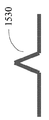
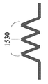
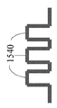
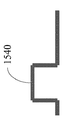
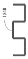
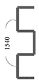
도 15a-15i는 셔터 함몰부들에 적합한 예시적인 대안적인 단면 형성들을 도시한다.
도 16a는 각져있는 주변 표면들을 갖는 예시적인 셔터의 상면도를 도시한다.
도 16b는 도 16a의 셔터의 단면도를 도시한다.
도 17은 각져있는 주변 표면들을 갖는 셔터를 형성하기 위한 예시적인 몰드의 단면도를 도시한다.
도 18은 각져있는 주변 표면들을 갖는 셔터를 포함하는 예시적인 디스플레이 장치의 단면도를 도시한다.
도 19는 각져있는 주변 표면들을 갖는 셔터를 포함하는 다른 예시적인 디스플레이 장치의 단면도를 도시한다.
도 20은 각져있는 주변 표면들을 갖는 셔터(2002)를 포함하는 다른 예시적인 디스플레이 장치(2000)의 일부의 단면도를 도시한다.Figure 1A shows an exemplary schematic diagram of a direct-view microelectromechanical systems (MEMS) -based display device.
Figure IB shows an exemplary block diagram of a host device.
Figure 2 shows an exemplary overview of an exemplary shutter-based optical modulator.
Figure 3A shows an exemplary schematic diagram of the control matrix.
Figure 3b shows an overview of an array of shutter-based optical modulators connected to the control matrix of Figure 3a.
Figures 4A and 4B illustrate exemplary views of a dual actuator shutter assembly.
Figure 5 shows an exemplary cross-sectional view of a display device including shutter-based optical modulators.
6A-6E illustrate cross-sectional views of stages of an exemplary composite shutter assembly configuration.
Figures 7A-7D illustrate isometric views of stages of an exemplary shutter assembly configuration with narrow side wall beams.
Figure 8 shows a top view of a shutter assembly including a looped drive beam.
Figure 9 shows an isometric view of a shutter assembly constructed in accordance with a 3-mask process.
Figure 10 illustrates an exemplary mold suitable for manufacturing the shutter assembly of Figure 9;
11 shows a top view of another exemplary shutter assembly.
Figure 12 shows an isometric view of another exemplary shutter assembly.
13 shows a cross-sectional view of a portion of an exemplary display device.
Figure 14 shows a cross-sectional view of a portion of another exemplary display device.
Figures 15A-15I illustrate exemplary alternative cross-sectional configurations suitable for shutter depressions.
Figure 16a shows a top view of an exemplary shutter with angled peripheral surfaces.
16B shows a sectional view of the shutter of Fig. 16A.
Figure 17 shows a cross-sectional view of an exemplary mold for forming a shutter having angled peripheral surfaces.
Figure 18 shows a cross-sectional view of an exemplary display device including a shutter having angled peripheral surfaces.
Figure 19 illustrates a cross-sectional view of another exemplary display device including a shutter having angled peripheral surfaces.
20 shows a cross-sectional view of a portion of another
특정한 디스플레이 장치는, 기계적인 셔터들을 사용하여 광을 변조함으로써 이미지들을 생성하도록 설계된다. 이들 셔터들은, 셔터에 부가하여, 셔터를 액츄에이팅하기 위한 액츄에이터들, 및 기판 위에 셔터를 지지하기 위한 앵커들을 포함하는 셔터 어셈블리들에 의해 지지 및 액츄에이팅된다. 그러나, 셔터들은 그들의 원하는 구성으로부터 변형되는 경향을 갖는다. 이러한 경향은, 셔터에 3차원 피쳐들을 포함시킴으로써 대항될 수 있다. 그러한 3차원 피쳐의 일 예는, 셔터의 평면으로부터 바깥으로 연장하고, 광 방출 어퍼쳐를 향해 개방되는 리브(rib) 또는 함몰부이다.A particular display device is designed to produce images by modulating light using mechanical shutters. These shutters, in addition to the shutters, are supported and actuated by actuators for actuating the shutters, and shutter assemblies including anchors for supporting the shutters on the substrate. However, the shutters have a tendency to deform from their desired configuration. This tendency can be countered by including three dimensional features in the shutter. One example of such a three-dimensional feature is a rib or depression that extends outwardly from the plane of the shutter and opens toward the light emission aperture.
부가적으로, 몇몇 셔터 어셈블리들은, 폐쇄 포지션에 있는 경우라도 광이 어퍼쳐로부터 의도적이지 않게 탈출하게 하기 위한 경향을 나타낸다. 이러한 광 누설은 3개의 인자들에 기여될 수 있다. 먼저, 셔터의 광 차단 부분에 의해 차단된 광은 셔터로부터, 그 후, 백라이트로부터 광을 방출하는 하부(underlying) 어퍼쳐 층으로부터, 그리고 최종적으로는 디스플레이로부터 반사될 수 있다. 둘째로, 광은, 셔터 어퍼쳐 내에 로케이팅된 특정한 수직 보강 벽들이 이웃한 광 차단 표면에서 종결(terminate)되는 위치들에서 셔터를 통해 누설될 수 있다. 셋째로, 큰 각도로 어퍼쳐 층 내의 어퍼쳐를 관통하는 광은 셔터의 에지를 충격(strike)할 수 있으며, 그 결과, 디스플레이 법선을 향해 그리고 디스플레이로부터 역으로 굴절될 수 있다.Additionally, some shutter assemblies exhibit a tendency to cause light to escape unintentionally from the aperture, even in the closed position. This light leakage can be attributed to three factors. First, the light blocked by the light blocking portion of the shutter can be reflected from the shutter, then from the underlying aperture layer that emits light from the backlight, and ultimately from the display. Second, the light can leak through the shutter at locations where certain vertical reinforcing walls that are located in the shutter aperture are terminated at neighboring light blocking surfaces. Third, light passing through the aperture in the aperture layer at a large angle can strike the edge of the shutter and, as a result, can be deflected toward the display normal and back from the display.
광 누설의 이들 소스들 각각은, 셔터 부가적인 강직성(rigidity)을 제공하고 셔터가 변형하기 위한 경향을 극복하는 동일한 3차원 피쳐들에 대한 변형들에 의해 부분적으로 해결될 수 있다. 상술된 반사 현상으로부터 초래하는 광 누설은, 셔터의 광 차단 부분의 사이즈 및/또는 어퍼쳐의 사이즈과 비교하여 비교적 큰 립들 또는 함몰부들을 포함하는 셔터에 의해 완화될 수 있다. 셔터의 길이를 따라 런(run)하는 립들 또는 함몰부들을 사용함으로써, 광 누설은 완화될 수 있고, 셔터 강직성은 증가될 수 있다. 굴절로 인한 광 누설은, 셔터의 다양한 주변 표면들을 각지게 하여 그들이 디스플레이 법선에 평행하거나 수직하지 않게 함으로써 완화될 수 있다.Each of these sources of light leakage can be partially resolved by modifications to the same three-dimensional features that provide additional rigidity of the shutter and overcome the tendency for the shutter to deform. The light leakage resulting from the above-mentioned reflection phenomenon can be alleviated by a shutter including relatively large lips or depressions in comparison with the size of the light blocking portion of the shutter and / or the size of the aperture. By using lips or depressions that run along the length of the shutter, light leakage can be mitigated and the shutter rigidity can be increased. Light leakage due to refraction can be mitigated by angling the various peripheral surfaces of the shutter so that they are not parallel or perpendicular to the display normal.
본 발명에 설명된 요지의 특정한 구현들은 다음의 잠재적인 이점들 중 하나 또는 그 초과를 실현하도록 구현될 수 있다. 셔터의 광 차단 부분들로의 비교적 넓은 측면 함몰부들의 포함물(inclusion)은, 자신의 원하는 형상을 유지할 가능성이 더 높은 더 견고한 셔터를 제공한다. 그러한 함몰부들은 또한, 광이 폐쇄되도록 의도된 픽셀로부터 디스플레이 외부로 누설되는 것을 방지하는 것을 도우며, 그에 의해, 디스플레이의 콘트라스트 비율을 개선시킨다. 셔터의 측면들을 따른 함몰부들은 유사하게, 광 누설을 방지하고 증가된 견고함들을 제공하는 것을 돕는다. 셔터의 각진 주면 표면들은 광 누설, 즉, 셔터 에지들로부터의 굴절의 다른 소스를 완화시킬 수 있고, 몇몇 경우들에서는 제거할 수 있으며, 콘트라스트 비율을 추가적으로 개선시킨다.Certain implementations of the subject matter described in the present invention may be implemented to realize one or more of the following potential advantages. The inclusion of relatively wide side depressions into the light blocking portions of the shutter provides a more rugged shutter that is more likely to maintain its desired shape. Such depressions also help prevent light from leaking out of the display from pixels intended to be closed, thereby improving the contrast ratio of the display. The depressions along the sides of the shutter similarly help to prevent light leakage and provide increased rigidity. The angled major surfaces of the shutter can relax other sources of light leakage, i. E. Refraction from the shutter edges, and in some cases can be eliminated, further improving the contrast ratio.
도 1a는 직시형 마이크로기계적 시스템(MEMS)-기반 디스플레이 장치(100)의 개략도를 도시한다. 디스플레이 장치(100)는, 행(row)들 및 열(column)들로 배열된 복수의 광 변조기들(102a-102d)(일반적으로, "광 변조기들(102)")을 포함한다. 디스플레이 장치(100)에서, 광 변조기들(102a 및 102d)은 개방 상태에 있으며, 광이 전달되게 한다. 광 변조기들(102b 및 102c)은 폐쇄 상태에 있으며, 광의 전달을 방해한다. 광 변조기들(102a-102d)의 상태들을 선택적으로 셋팅함으로써, 디스플레이 장치(100)는, 램프 또는 램프들(105)에 의해 조명되면, 백리트(backlit) 디스플레이에 대한 이미지(104)를 형성하는데 이용될 수 있다. 다른 구현에서, 장치(100)는 장치의 전면으로부터 발신하는 주변광의 반사에 의해 이미지를 형성할 수도 있다. 다른 구현에서, 장치(100)는, 디스플레이의 전면에 포지셔닝된 램프 또는 램프들로부터의 광의 반사에 의해, 전면 광의 사용에 의해 이미지를 형성할 수도 있다.FIG. 1A shows a schematic view of a direct-view micromechanical system (MEMS) -based
몇몇 구현들에서, 각각의 광 변조기(102)는 이미지(104) 내의 픽셀(106)에 대응한다. 몇몇 다른 구현들에서, 디스플레이 장치(100)는 이미지(104)에서 픽셀(106)을 형성하기 위해 복수의 광 변조기들을 이용할 수도 있다. 예를 들어, 디스플레이 장치(100)는 3개의 컬러-특정 광 변조기들(102)을 포함할 수도 있다. 특정한 픽셀(106)에 대응하는 컬러-특정 광 변조기들(102) 중 하나 또는 그 초과를 선택적으로 개방함으로써, 디스플레이 장치(100)는 이미지(104)에서 컬러 픽셀(106)을 생성할 수 있다. 다른 예에서, 디스플레이 장치(100)는, 이미지(104)에서 루미넌스 레벨을 제공하기 위해 픽셀(106) 당 2개 또는 그 초과의 광 변조기들(102)을 포함한다. 이미지에 관해, "픽셀"은 이미지의 해상도에 의해 정의된 가장 작은 화상 엘리먼트에 대응한다. 디스플레이 장치(100)의 구조 컴포넌트들에 관해, 용어 "픽셀"은, 이미지의 단일 픽셀을 형성하는 광을 변조하기 위해 이용되는 결합된 기계적 및 전기적 컴포넌트들을 지칭한다.In some implementations, each optical modulator 102 corresponds to a
디스플레이 장치(100)는, 그것이 투영 애플리케이션들에서 통상적으로 발견되는 이미징 옵틱스(optics)를 포함하지 않을 수도 있다는 점에서 직시형 디스플레이다. 투영 디스플레이에서, 디스플레이 장치의 표면 상에 형성된 이미지는 스크린 또는 벽 상으로 투영된다. 디스플레이 장치는 투영된 이미지보다 실질적으로 작다. 직시형 디스플레이에서, 사용자는, 디스플레이 상에서 관측되는 밝기 및/또는 콘트라스트를 향상시키기 위해 광 변조기들 및 선택적으로는 백라이트 또는 전면 광을 포함하는 디스플레이 장치를 직접 봄으로써 이미지를 관측한다.
직시형 디스플레이들은 투과 또는 반사 모드 중 어느 하나로 동작할 수도 있다. 투과 디스플레이에서, 광 변조기들은, 디스플레이 뒤에 포지셔닝된 램프 또는 램프들로부터 발신하는 광을 필터링하거나 선택적으로는 차단한다. 램프들로부터의 광은, 각각의 픽셀이 균일하게 조명될 수 있도록 광가이드 또는 "백라이트"로 선택적으로 주입된다. 투과 직시형 디스플레이들은 종종, 광 변조기들을 포함하는 하나의 기판이 백라이트의 상단 상에 직접 포지셔닝되는 샌드위치 어셈블리 어레인지먼트(arragement)를 용이하게 하기 위해 투명한 또는 유리 기판들 상으로 구축된다.The direct view displays may operate in either a transmissive or reflective mode. In the transmissive display, the light modulators filter or selectively block the light from the lamp or lamps positioned behind the display. The light from the lamps is selectively injected into the light guide or "backlight" so that each pixel can be uniformly illuminated. Transparent direct displays are often built on transparent or glass substrates to facilitate sandwich assembly arragement where one substrate, including optical modulators, is directly positioned on top of the backlight.
각각의 광 변조기(102)는 셔터(108) 및 어퍼쳐(109)를 포함할 수 있다. 이미지(104)에서 픽셀(106)을 조명하기 위해, 셔터(108)는, 그 셔터가 광이 뷰어를 향하여 어퍼쳐(109)를 관통하게 하도록 포지셔닝된다. 픽셀(106)을 언리트(unlit)하게 유지하기 위해, 셔터(108)는, 그 셔터가 어퍼쳐(109)를 통한 광의 전달을 방해하도록 포지셔닝된다. 어퍼쳐(109)는, 각각의 광 변조기(102)에서 반사 또는 광-흡수 재료를 통해 패터닝된 개구에 의해 정의된다.Each of the optical modulators 102 may include a
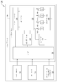
디스플레이 장치는 또한, 셔터들의 이동을 제어하기 위해 기판 및 광 변조기들에 접속된 제어 매트릭스를 포함한다. 제어 매트릭스는, 픽셀들의 행 당 적어도 하나의 기입-인에이블 상호접속부(110)(또한, "스캔-라인 상호접속부"로 지칭됨)를 포함하는 일련의 전기 상호접속부들(예를 들어, 상호접속부들(110, 112 및 114))을 포함하며, 하나의 데이터 상호접속부(112)는 픽셀들의 각각의 열에 대한 것이고, 하나의 공통적인 상호접속부(114)는 모든 픽셀들에, 또는 적어도, 디스플레이 장치(100) 내의 다수의 열들 및 다수의 행들 둘 모두로부터의 픽셀들에 공통 전압을 제공한다. 적절한 전압("기입-인에이블링 전압 VWE")의 인가에 응답하여, 픽셀들의 주어진 행에 대한 기입-인에이블 상호접속부(110)는, 새로운 셔터 이동 명령들을 수용하기 위해 행에서 픽셀들을 준비한다. 데이터 상호접속부들(112)은 데이터 전압 펄스들의 형태로 새로운 이동 명령들을 통신한다. 몇몇 구현들에서, 데이터 상호접속부들(112)에 인가된 데이터 전압 펄스들은, 셔터들의 정전식 이동에 직접 기여한다. 몇몇 다른 구현들에서, 데이터 전압 펄스들은, 광 변조기들(102)로의 별개의 액츄에이션 전압들의 인가를 제어하는 스위치들, 예를 들어, 트랜지스터들 또는 다른 비선형 회로 엘리먼트들을 제어하며, 그 전압들은 통상적으로, 데이터 전압들보다 크기가 더 높다. 그 후, 이들 액츄에이션 전압들의 인가는 셔터들(108)의 정전식 드라이빙된 이동을 초래한다.The display device also includes a control matrix connected to the substrate and the light modulators to control movement of the shutters. The control matrix includes a series of electrical interconnects (e.g., interconnects) that include at least one write-enable
도 1b는 호스트 디바이스(즉, 셀 폰, 스마트폰, PDA, MP3 플레이어, 태블릿, e-리터 등)의 블록도(120)의 일 예를 도시한다. 호스트 디바이스는 디스플레이 장치(128), 호스트 프로세서(122), 환경 센서들(124), 사용자 입력 모듈(126), 및 전력 소스를 포함한다.1B illustrates an example of a block diagram 120 of a host device (i.e., cell phone, smartphone, PDA, MP3 player, tablet, e-liter, etc.). The host device includes a
디스플레이 장치(128)는, 복수의 스캔 드라이버들(130)(또한 "기입 인에이블링 전압 소스들"로 지칭됨), 복수의 데이터 드라이버들(132)(또한, "데이터 전압 소스들"로 지칭됨), 제어기(134), 공통 드라이버들(138), 램프들(140-146), 및 램프 드라이버들(148)을 포함한다. 스캔 드라이버들(130)은 기입 인에이블링 전압들을 스캔-라인 상호접속부들(110)에 인가한다. 데이터 드라이버들(132)은 데이터 전압들을 데이터 상호접속부들(112)에 인가한다.
디스플레이 장치의 몇몇 구현들에서, 데이터 드라이버들(132)은, 특히, 이미지(104)의 루미넌스 레벨이 아날로그 방식으로 도출될 경우, 광 변조기들에 아날로그 데이터 전압들을 제공하도록 구성된다. 아날로그 동작에서, 일 범위의 중간 전압들이 데이터 상호접속부들(112)을 통해 인가되는 경우, 셔터들(108)에서 일 범위의 중간 개방 상태들, 및 그에 따라 이미지(104)에서 일 범위의 중간 조명 상태들 또는 루미넌스 레벨들을 초래하도록 광 변조기들(102)이 설계된다. 다른 경우들에서, 데이터 드라이버들(138)은, 2, 3, 또는 4개의 디지털 전압 레벨들의 감소된 세트만을 데이터 상호접속부들(112)에 인가하도록 구성된다. 이들 전압 레벨들은, 셔터들(108) 각각에 대해 개방 상태, 폐쇄 상태, 또는 다른 별개의 상태를 디지털 방식으로 셋팅하도록 설계된다.In some implementations of the display device, the data drivers 132 are configured to provide analog data voltages to the optical modulators, particularly when the luminance level of the
스캔 드라이버들(130) 및 데이터 드라이버들(132)은, 디지털 제어기 회로(134)(또한 "제어기(134)"로 지칭됨)에 접속된다. 제어기는 행들 및 이미지 프레임들에 의해 그룹화된 미리 결정된 시퀀스들로 조직화된 주로 직렬 방식으로 데이터 드라이버들(132)에 데이터를 전송한다. 데이터 드라이버들(132)은 직렬 투 병렬 데이터 변환기들, 레벨 시프팅, 및 몇몇 애플리케이션들에 대해서는 디지털 투 아날로그 전압 변환기들을 포함할 수 있다.
디스플레이 장치는 선택적으로, 공통 전압 소스들로 또한 지칭되는 공통 드라이버들(138)의 세트를 포함한다. 몇몇 구현들에서, 공통 드라이버들(138)은, 예를 들어, 일련의 공통 상호접속부들(114)에 전압을 공급함으로써 광 변조기들의 어레이 내의 모든 광 변조기들에 DC 공통 전위를 제공한다. 몇몇 다른 구현들에서, 제어기(134)로부터의 커맨드들에 따르는 공통 드라이버들(138)은, 전압 펄스들 또는 신호들, 예를 들어, 어레이의 다수의 행들 및 열들 내의 모든 광 변조기들의 동시적인 액츄에이션을 드라이빙 및/또는 개시할 수 있는 글로벌 액츄에이션 펄스들을 광 변조기들의 어레이로 이슈한다.The display device optionally includes a set of common drivers 138, also referred to as common voltage sources. In some implementations, common drivers 138 provide a DC common potential to all of the optical modulators in the array of optical modulators, for example, by supplying a voltage to a series of
상이한 디스플레이 기능들에 대한 드라이버들(예를 들어, 스캔 드라이버들(130), 데이터 드라이버들(132) 및 공통 드라이버들(138)) 모두는 제어기(134)에 의해 시간-동기화된다. 제어기로부터의 타이밍 커맨드들은, 램프 드라이버들(148), 픽셀들의 어레이 내의 특정한 행들의 기입-인에이블링 및 시퀀싱, 데이터 드라이버들(132)로부터의 전압들의 출력, 및 광 변조기 액츄에이션을 위해 제공되는 전압들의 출력을 통해 레드, 그린 및 블루 및 화이트 램프들(각각, 140, 142, 144 및 146)의 조명을 조정한다.All of the drivers (e.g., scan
제어기(134)는, 셔터들(108) 각각이 새로운 이미지(104)에 적절한 조명 레벨들로 리셋팅(re-set)될 수 있는 시퀀싱 또는 어드레싱 방식을 결정한다. 새로운 이미지들(104)은 주기적인 간격들로 셋팅될 수 있다. 예를 들어, 비디오 디스플레이들에 대해, 비디오의 컬러 이미지들(104) 또는 프레임들은 10으로부터 300헤르츠(Hz)의 범위에 있는 주파수들로 리프레쉬(refresh)된다. 몇몇 구현들에서, 어레이에 대한 이미지 프레임의 셋팅은, 교변하는 이미지 프레임들이 레드, 그린 및 블루와 같이 교변하는 일련의 컬러들로 조명되도록 램프들(140, 142, 144 및 146)의 조명과 동기화된다. 각각의 개별 컬러에 대한 이미지 프레임들은 컬러 서브프레임으로 지칭된다. 필드 순차적인 컬러 방법으로 지칭되는 이러한 방법에서, 컬러 서브프레임들이 20Hz를 초과하는 주파수들로 교변되면, 인간의 두뇌는 교변하는 프레임 이미지들을 넓고 연속적인 범위의 컬러들을 갖는 이미지의 인식으로 평균할 것이다. 대안적인 구현들에서, 프라이머리 컬러(primary color)를 갖는 4개 또는 그 초과의 램프들이 디스플레이 장치(100)에서 이용될 수 있으며, 레드, 그린 및 블루 이외의 프라이머리들을 이용한다.The
몇몇 구현들에서, 디스플레이 장치(100)가 개방 및 폐쇄 상태들 사이에서의 셔터들(108)의 디지털 스위칭에 대해 설계되는 경우, 제어기(134)는 상술된 바와 같이, 시분할 그레이 스캐일의 방법에 의해 이미지를 형성한다. 몇몇 다른 구현들에서, 디스플레이 장치(100)는 픽셀 당 다수의 셔터들(108)의 사용을 통해 그레이 스캐일을 제공할 수 있다.In some implementations, when the
몇몇 구현들에서, 이미지 상태(104)에 대한 데이터는, 스캔 라인들로 또한 지칭되는 개별적인 행들의 순차적인 어드레싱에 의하여 변조기 어레이로 제어기(134)에 의해 로딩된다. 시퀀스 내의 각각의 행 또는 스캔 라인에 대해, 스캔 드라이버(130)는 어레이의 그 행에 대한 기입 인에이블 상호접속부(110)에 기입-인에이블 전압을 인가하고, 후속하여, 데이터 드라이버(132)는 선택된 행 내의 각각의 열에 대해, 원하는 셔터 상태들에 대응하는 데이터 전압들을 공급한다. 이러한 프로세스는, 데이터가 어레이 내의 모든 행들에 대해 로딩될 때까지 반복된다. 몇몇 구현들에서, 데이터 로딩을 위한 선택된 행들의 시퀀스는 선형이며, 어레이에서 상단으로부터 하단으로 진행한다. 몇몇 다른 구현들에서, 선택된 행들의 시퀀스는, 시각적인 아티팩트(artifact)들을 최소화시키기 위해 의사-랜덤화된다. 그리고, 몇몇 다른 구현들에서, 시퀀싱은 블록들에 의해 조직화되며, 여기서, 블록에 대해, 이미지 상태(104)의 오직 특정한 부분에 대한 데이터가, 예를 들어, 시퀀스 내의 어레이의 매 5번째 행만을 어드레싱함으로써 어레이로 로딩된다.In some implementations, data for the
몇몇 구현들에서, 이미지 데이터를 어레이로 로딩하기 위한 프로세스는, 셔터들(108)을 액츄에이팅하는 프로세스로부터 시간적으로 분리된다. 이들 구현들에서, 변조기 어레이는, 어레이 내의 각각의 픽셀에 대한 데이터 메모리 엘리먼트들을 포함할 수도 있으며, 제어 매트릭스는, 메모리 엘리먼트들에 저장된 데이터에 따라 셔터들(108)의 동시적인 액츄에이션을 개시하기 위해, 공통 드라이버(138)로부터 트리거 신호들을 반송(carry)하기 위한 글로벌 액츄에이션 상호접속부를 포함할 수도 있다.In some implementations, the process for loading the image data into the array is temporally separated from the process of actuating the
대안적인 구현들에서, 픽셀들의 어레이 및 픽셀들을 제어하는 제어 매트릭스는 직사각형 행들 및 열들 이외의 구성들로 배열될 수도 있다. 예를 들어, 픽셀들은 육각형 어레이들 또는 곡선 행들 및 열들로 배열될 수 있다. 일반적으로, 본 명세서에서 사용된 바와 같이, 용어 스캔-라인은 기입-인에이블링 상호접속부를 공유하는 임의의 복수의 픽셀들을 지칭할 것이다.In alternative implementations, the array of pixels and the control matrix that controls the pixels may be arranged in configurations other than rectangular rows and columns. For example, the pixels may be arranged in hexagonal arrays or in curved rows and columns. Generally, as used herein, the term scan-line will refer to any of a plurality of pixels sharing a write-enable interconnect.
호스트 프로세서(122)는 일반적으로 호스트의 동작들을 제어한다. 예를 들어, 호스트 프로세서는, 휴대용 전자 디바이스를 제어하기 위한 범용 또는 특수 목적 프로세서일 수도 있다. 호스트 디바이스(120) 내에 포함되는 디스플레이 장치(128)에 대해, 호스트 프로세서는 이미지 데이터 뿐만 아니라 호스트에 관한 부가적인 데이터를 출력한다. 그러한 정보는, 주변 광 또는 온도와 같은 환경 센서들로부터의 데이터; 예를 들어, 호스트의 동작 모드 또는 호스트의 전력 소스에 남아있는 전력의 양을 포함하는 호스트에 관한 정보; 이미지 데이터의 콘텐츠에 관한 정보; 이미지 데이터의 타입에 관한 정보; 및/또는 이미지 모드를 선택할 시에 사용하기 위한 디스플레이 장치에 대한 명령들을 포함할 수도 있다.The
사용자 입력 모듈(126)은, 직접적으로 또는 호스트 프로세서(122)를 통해 사용자의 개인 선호도들을 제어기(134)에 운반한다. 몇몇 구현들에서, 사용자 입력 모듈은, 더 짙은 컬러", "더 양호한 콘트라스트", "더 낮은 전력", "증가된 밝기", "스포츠", "라이브 액션", 또는 "애니메이션"과 같은 개인 선호도들을 사용자가 프로그래밍하는 소프트웨어에 의해 제어된다. 몇몇 다른 구현들에서, 이들 선호도들은 스위치 또는 다이얼과 같은 하드웨어를 사용하여 호스트에 입력된다. 제어기(134)로의 복수의 데이터 입력들은, 최적의 이미징 특징들에 대응하는 다양한 드라이버들(130, 132, 138 및 148)에 데이터를 제공하도록 제어기에 지시한다.The
환경 센서 모듈(124)은 또한, 호스트 디바이스의 일부로서 포함될 수 있다. 환경 센서 모듈은, 온도 및 주변 광 조건들과 같은 주변 환경에 관한 데이터를 수신한다. 센서 모듈(124)은, 디바이스가 인도어 또는 오피스 환경 대 밝은 주중의 아웃도어 환경 및 야간의 아웃도어 환경에서 동작하고 있는지를 구별하도록 프로그래밍될 수 있다. 센서 모듈은 이러한 정보를 디스플레이 제어기(134)에 통신하여, 제어기가 주변 환경에 응답하여 뷰잉 조건들을 최적화시킬 수 있게 한다.The
도 2는 예시적인 셔터-기반 광 변조기(200)의 개관도를 도시한다. 셔터-기반 광 변조기는, 도 1a의 직시형 MEMS-기반 디스플레이 장치(100)로의 포함에 적합하다. 광 변조기(200)는 액츄에이터(204)에 커플링된 셔터(202)를 포함한다. 액츄에이터(204)는, 2개의 별개의 컴플리안트(compliant) 전극 빔 액츄에이터들(205)("액츄에이터들(205)")로부터 형성될 수 있다. 셔터(202)는 하나의 측면 상에서 액츄에이터들(205)에 커플링한다. 액츄에이터들(205)은, 표면(203)에 실질적으로 평행한 모션의 평면에서, 기판(203) 위에서 셔터(202)를 횡단하게 이동시킨다. 셔터(202)의 반대 측은, 액츄에이터(204)에 의해 가해진 힘들에 반대인 회복력(restore force)을 제공하는 스프링(207)에 커플링된다.FIG. 2 shows an overview of an exemplary shutter-based
각각의 액츄에이터(205)는 셔터(202)를 로드 앵커(208)에 접속시키는 컴플리안트 로드 빔(206)을 포함한다. 컴플리안트 로드 빔들(206)과 함께 로드 앵커들(208)은 기계적 지지부들로서 기능하여, 셔터(202)를 표면(203)에 근접하여 서스펜딩(suspend)되게 유지한다. 표면은 광의 전달을 허용하기 위한 하나 또는 그 초과의 어퍼쳐 홀들(211)을 포함한다. 로드 앵커들(208)은 컴플리안트 로드 빔들(206) 및 셔터(202)를 표면(203)에 물리적으로 접속시키고, 로드 빔들(206)을 바이어스 전압, 몇몇 예시들에서는 접지에 전기적으로 접속시킨다.Each
기판이 실리콘과 같이 불투명하면, 어퍼쳐 홀들(211)은, 기판(204)을 통해 홀들의 어레이를 에칭함으로써 기판에 형성된다. 기판(204)이 유리 또는 플라스틱과 같이 투명하면, 어퍼쳐 홀들(211)은 기판(203) 상에 증착된 광-차단 재료의 층에서 형성된다. 어퍼쳐 홀들(211)은 일반적으로 형상이 원형, 타원형, 다각형, S자형(serpentine), 또는 불규칙할 수 있다.If the substrate is opaque, such as silicon, then the aperture holes 211 are formed in the substrate by etching the array of holes through the
각각의 액츄에이터(205)는 또한, 각각의 로드 빔(206)에 인접하여 포지셔닝된 컴플리안트 드라이브 빔(216)을 포함한다. 드라이브 빔들(216)은 하나의 단부에서, 드라이버 빔들(216) 사이에 공유된 드라이브 빔 앵커(218)에 커플링한다. 각각의 드라이브 빔(216)의 다른 단부는 이동이 자유롭다. 각각의 드라이브 빔(216)은, 그것이 드라이브 빔(216)의 자유단에 인접한 로드 빔(206) 및 로드 빔(206)의 앵커링된 단부에 가장 가깝도록 만곡(curve)된다.Each
동작에서, 광 변조기(200)를 포함하는 디스플레이 장치는, 드라이브 빔 앵커(218)를 통해 드라이브 빔들(216)에 전기 전위를 인가한다. 제 2 전기 전위는 로드 빔들(206)에 인가될 수도 있다. 드라이브 빔들(216)과 로드 빔들(206) 사이의 결과적인 전위 차이는, 로드 빔들(206)의 앵커링된 단부들을 향해 드라이브 빔들(216)의 자유단들을 끌어당기고, 드라이브 빔들(216)의 앵커링된 단부들을 향해 로드 빔들(206)의 셔터 단부들을 끌어당기며, 그에 의해, 드라이브 앵커(218)를 향해 횡단하게 셔터(202)를 드라이빙시킨다. 컴플리안트 부재들(206)은 스프링들로서 작동하며, 예컨대, 빔들(206 및 216) 전위에 걸친 전압이 제거되는 경우, 로드 빔들(206)은 셔터(202)를 다시 그의 초기 포지션으로 밀며, 로드 빔들(206)에 저장된 스트레스를 릴리즈(release)한다.In operation, the display device including the
광 변조기(200)와 같은 광 변조기는, 전압들이 제거된 이후 자신의 정지(rest) 포지션으로 셔터를 리턴시키기 위해 스프링과 같이 패시브 회복력을 포함한다. 다른 셔터 어셈블리들은, 개방 또는 폐쇄 상태 어느 하나로 셔터를 이동시키기 위해 "개방" 및 "패쇄된" 액츄에이터들의 듀얼 세트 및 "개방" 및 "폐쇄" 전극들의 별개의 세트들을 포함할 수 있다.An optical modulator, such as
다양한 방법들이 존재하며, 그 방법들에 의해, 셔터들 및 어퍼쳐들의 어레이는 이미지들, 많은 경우들에서는 동영상들을 적절한 루미넌스 레벨들로 생성하도록 제어 매트릭스를 통해 제어될 수 있다. 몇몇 경우들에서, 제어는, 디스플레이의 주변부 상의 드라이버 회로들에 접속된 행 및 열 상호접속부들의 패시브 매트릭스 어레이에 의해 달성된다. 다른 경우들에서, 디스플레이의 속도, 루미넌스 레벨 및/또는 전력 소산(dissipation) 성능을 개선시키기 위해 어레이의 각각의 픽셀(소위 액티브 매트릭스) 내에 스위칭 및/또는 데이터 저장 엘리먼트들을 포함시키는 것이 적절하다.There are various methods by which the array of shutters and apertures can be controlled through the control matrix to produce images, in many cases moving images, with the appropriate luminance levels. In some cases, control is achieved by a passive matrix array of row and column interconnects connected to driver circuits on the periphery of the display. In other cases, it is appropriate to include switching and / or data storage elements within each pixel (so-called active matrix) of the array to improve the speed, luminance level, and / or power dissipation performance of the display.
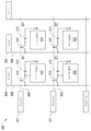
도 3a는 제어 매트릭스(300)의 예시적인 개략도를 도시한다. 제어 매트릭스(300)는, 도 1a의 MEMS-기반 디스플레이 장치(100)로 포함되는 광 변조기들을 제어하기에 적절하다. 도 3b는, 도 3a의 제어 매트릭스(300)에 접속된 셔터-기반 광 변조기들의 어레이(320)의 개관도를 도시한다. 제어 매트릭스(300)는 픽셀들의 어레이(320)("어레이(320)")를 어드레싱할 수도 있다. 각각의 픽셀(301)은, 액츄에이터(303)에 의해 제어되는 도 2의 셔터 어셈블리(200)와 같은 탄력성 셔터 어셈블리(302)를 포함할 수 있다. 각각의 픽셀은 또한, 어퍼쳐들(324)을 포함하는 어퍼쳐 층(322)을 포함할 수 있다.FIG. 3A shows an exemplary schematic diagram of the
제어 매트릭스(300)는, 셔터 어셈블리들(302)이 형성되는 기판(304)의 표면 상에서 분산형 또는 박막-증착된 전기 회로로서 제조된다. 제어 매트릭스(300)는, 제어 매트릭스(300) 내의 픽셀들(301)의 각각의 행에 대한 스캔-라인 상호접속부(306), 및 제어 매트릭스(300) 내의 픽셀들(301)의 각각의 열에 대한 데이터-상호접속부(308)를 포함한다. 각각의 스캔-라인 상호접속부(306)는 픽셀들(301)의 대응하는 행에서 픽셀들(301)에 기입-인에이블링 전압 소스(307)를 전기적으로 접속시킨다. 각각의 데이터 상호접속부(308)는 픽셀들의 대응하는 열에서 픽셀들(301)에 데이터 전압 소스(309)("Vd 소스")를 전기적으로 접속시킨다. 제어 매트릭스(300)에서, Vd 소스(309)는 셔터 어셈블리들(302)의 액츄에이션을 위해 사용될 대부분의 에너지를 제공한다. 따라서, 데이터 전압 소스, 즉 Vd 소스(309)는 또한 액츄에이션 전압 소스로서 기능한다.The
도 3a 및 도 3b를 참조하면, 각각의 픽셀(301)에 대해 또는 픽셀들의 어레이(320) 내의 각각의 셔터 어셈블리(302)에 대해, 제어 매트릭스(300)는 트랜지스터(310) 및 커패시터(312)를 포함한다. 각각의 트랜지스터(310)의 게이트는, 픽셀(301)이 로케이팅되는 어레이(320) 내의 행의 스캔-라인 상호접속부(306)에 전기적으로 접속된다. 각각의 트랜지스터(310)의 소스는 자신의 대응하는 데이터 접속부(308)에 전기적으로 접속된다. 각각의 셔터 어셈블리(302)의 액츄에이터들(303)은 2개의 전극들을 포함한다. 각각의 트랜지스터(310)의 드레인은, 대응하는 커패시터(312)의 하나의 전극 및 대응하는 액츄에이터(303)의 전극들 중 하나에 병행하게 전기적으로 접속된다. 셔터 어셈블리(302) 내의 커패시터(312)의 다른 전극 및 액츄에이터(303)의 다른 전극은 공통 또는 접지 전위에 접속된다. 대안적인 구현들에서, 트랜지스터들(310)은 반도체 다이오드들 및 금속-절연체-금속 샌드위치 타입 스위칭 엘리먼트들로 대체될 수 있다.3A and 3B, for each
동작에서, 이미지를 형성하기 위해, 제어 매트릭스(300)는, Vwe를 차례로 각각의 스캔-라인 상호접속부(306)에 인가함으로써 순차적으로 어레이(320) 내의 각각의 행을 기입-인에이블시킨다. 기입-인에이블된 행에 대해, 행 내의 픽셀들(301)의 트랜지스터들(310)의 게이트들로의 Vwe의 인가는, 셔터 어셈블리(302)의 액츄에이터(303)에 전위를 인가하기 위해 트랜지스터들(310)을 통한 데이터 상호접속부들(308)을 통한 전류의 흐름을 허용한다. 행이 기입-인에이블되는 동안, 데이터 전압들 Vd는 데이터 상호접속부들(308)에 선택적으로 인가된다. 아날로그 그레이 스캐일을 제공하는 구현들에서, 각각의 데이터 상호접속(308)에 인가된 데이터 전압은, 기입-인에이블된 스캔-라인 상호접속부(306) 및 데이터 상호접속부(308)의 교차점에 로케이팅된 픽셀(301)의 원하는 밝기와 관련하여 변경된다. 디지털 제어 방식들을 제공하는 구현들에서, 데이터 전압은, 비교적 낮은 크기 전압(즉, 접지 근처의 전압)이도록 또는 Vat(액츄에이션 임계 전압)을 충족 또는 초과하도록 선택된다. Vat의 데이터 상호접속부(308)로의 인가에 응답하여, 대응하는 셔터 어셈블리 내의 액츄에이터(303)가 액츄에이팅하여, 셔터 어셈블리(302)에서 셔터를 개방시킨다. 데이터 상호접속부(308)에 인가된 전압은, 제어 매트릭스(300)가 Vwe를 행에 인가하는 것을 중지한 이후더라도, 픽셀(301)의 커패시터(312)에 저장되어 유지된다. 따라서, 전압 Vwe는, 셔터 어셈블리(302)가 액츄에이팅하기에 충분히 긴 시간들 동안 대기 및 보유될 필요가 없으며; 그러한 액츄에이션은, 기입-인에이블링 전압이 행으로부터 제거된 이후 진행할 수 있다. 커패시터들(312)은 또한, 어레이(320) 내의 메모리 엘리먼트들로서 기능하며, 이미지 프레임의 조명을 위한 액츄에이션 명령들을 저장한다.In operation, to form an image,
어레이(320) 내의 픽셀들(301) 뿐만 아니라 제어 매트릭스(300)는 기판(304) 상에 형성된다. 어레이는 기판(304) 상에 배치된 어퍼쳐 층(322)을 포함하며, 그 층은 어레이(320) 내의 각각의 픽셀들(301)에 대한 어퍼쳐들(324)의 세트를 포함한다. 어퍼쳐들(324)은 각각의 픽셀에서 셔터 어셈블리들(302)로 정렬된다. 몇몇 구현들에서, 기판(304)은 유리 또는 플라스틱과 같은 투명 재료로 구성된다. 몇몇 다른 구현들에서, 기판(304)은 불투명한 재료로 구성되지만, 여기서, 홀들은 어퍼쳐들(324)을 형성하기 위해 에칭된다.The
액츄에이터(303)와 함께 셔터 어셈블리(302)는 쌍안정(bi-stable)으로 제조될 수 있다. 즉, 셔터들은 적어도 2개의 평형 포지션들(예를 들어, 개방 또는 폐쇄)에 존재할 수 있으며, 그들을 어느 하나의 포지션에서 홀딩하기 위한 전력이 거의 요구되지 않거나 요구되지 않는다. 일단 셔터 어셈블리(302)의 셔터가 적소에 셋팅되면, 어떠한 전기 에너지 또는 홀딩 전압도 그 포지션을 유지하기 위해 요구되지 않는다. 셔터 어셈블리(302)의 물리적 엘리먼트들에 대한 기계적인 스트레스들은 적소에 셔터를 홀딩할 수 있다.The
액츄에이터(303)와 함께 셔터 어셈블리(302)는 또한, 전기적으로 쌍안정으로 제조될 수 있다. 전기적으로 쌍안정인 셔터 어셈블리에서, 폐쇄 액츄에이터에 인가되면(셔터는 개방 또는 폐쇄중 어느 하나임), 반대의 힘이 셔터에 가해지더라도, 액츄에이터를 폐쇄로 및 셔터를 적소에 홀딩하는 셔터 어셈블리의 액츄에이션 전압 아래의 일 범위의 전압들이 존재한다. 반대의 힘은, 도 2에 도시된 셔터-기반 광 변조기(200) 내의 스프링(207)과 같은 스프링에 의해 가해질 수도 있거나, 반대의 힘은, "개방" 또는 "폐쇄" 액츄에이터와 같은 반대의 액츄에이터에 의해 가해질 수도 있다.The
광 변조기 어레이(320)는, 픽셀 당 단일 MEMS 광 변조기를 갖는 것으로 도시된다. 다수의 MEMS 광 변조기들이 각각의 픽셀에 제공되며, 그에 의해, 각각의 픽셀 내의 단지 바이너리 "온" 또는 "오프" 광학 상태들 이상의 가능성을 제공하는 다른 구현들이 가능하다. 특정한 형태들의 코딩된 영역 분할 그레이 스캐일이 가능하며, 여기서, 픽셀에서 다수의 MEMS 광 변조기들이 제공되고, 광 변조기들 각각과 연관된 어퍼쳐들(324)은 동일하지 않은 영역들을 갖는다.The
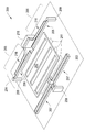
도 4a 및 4b는 듀얼 액츄에이터 셔터 어셈블리(400)의 예시적인 뷰들을 도시한다. 듀얼 액츄에이터 셔터 어셈블리는 도 4a에 도시된 바와 같이, 개방 상태에 있다. 도 4b는 폐쇄 상태의 듀얼 액츄에이터 셔터 어셈블리(400)를 도시한다. 셔터 어셈블리(200)와는 대조적으로, 셔터 어셈블리(400)는 셔터(406)의 어느 하나의 측면 상에 액츄에이터들(402 및 404)을 포함한다. 각각의 액츄에이터(402 및 404)는 독립적으로 제어된다. 제 1 액츄에이터, 즉 셔터-개방 액츄에이터(402)는 셔터(406)를 개방하도록 기능한다. 제 2 반대의 액츄에이터, 즉 셔터-폐쇄 액츄에이터(404)는 셔터(406)를 폐쇄하도록 기능한다. 액츄에이터들(402 및 404) 둘 모두는 컴플리안트 빔 전극 액츄에이터들이다. 액츄에이터들(402 및 404)은, 셔터가 서스펜딩되는 어퍼쳐 층(407)과 실질적으로 평면 평행하게 셔터(406)를 드라이빙함으로써 셔터(406)를 개방 및 폐쇄한다. 셔터(406)는, 액츄에이터들(402 및 404)에 부착된 앵커들(408)에 의해 어퍼쳐 층(407) 위에 짧은 거리로 서스펜딩된다. 자신의 이동축에 따라 셔터(406)의 둘 모두의 단자들에 부착된 지지부들의 포함물은, 셔터(406)의 평면 모션으로부터 감소되며, 기판에 평행한 평면으로 모션을 실질적으로 한정시킨다. 도 3a의 제어 매트릭스(300)와의 유사점에 의해, 셔터 어셈블리(400)와 함께 사용하기에 적합한 제어 매트릭스는, 반대의 셔터-개방 및 셔터-폐쇄 액츄에이터들(402 및 404) 각각에 대해 하나의 트랜지스터 및 하나의 커패시터를 포함할 수도 있다.Figures 4A and 4B illustrate exemplary views of a dual
셔터(406)는 광이 관통할 수 있는 2개의 셔터 어퍼쳐들(412)을 포함한다. 어퍼쳐 층(407)은 3개의 어퍼쳐들(409)의 세트를 포함한다. 도 4a에서, 셔터 어셈블리(400)는 개방 상태에 있고, 그러므로, 셔터-개방 액츄에이터(402)가 액츄에이팅되며, 셔터-폐쇄 액츄에이터(404)는 자신의 이완(relax) 포지션에 있고, 셔터 어퍼쳐들(412)의 중앙라인들은 어처펴 층 어퍼쳐들(409) 중 2개의 중앙라인과 일치한다. 도 4b에서, 셔터 어셈블리(400)는 폐쇄 상태로 이동되고, 그러므로, 셔터-개방 액츄에이터(402)는 자신의 완화 포지션에 있으며, 셔터-폐쇄 액츄에이터(404)는 액츄에이팅되고, 셔터(406)의 광 차단 부분들은 이제 어퍼쳐들(409)을 통한 광의 투과를 차단하기 위한 포지션에 있다(파선들로 도시됨).The
각각의 어퍼쳐는 자신의 주변 근처에 적어도 하나의 에지를 갖는다. 예를 들어, 직사각형 어퍼쳐들(409)은 4개의 에지들을 갖는다. 원형, 타원형, 계란형(oval), 또는 다른 만곡형 어퍼쳐들이 어퍼쳐 층(407)에 형성되는 대안적인 구현들에서, 각각의 어퍼쳐는 단일 에지만을 가질 수도 있다. 몇몇 다른 구현들에서, 어퍼쳐들은 수학적인 의미에서 분리되거나 분해될 필요가 없지만, 대신 접속될 수 있다. 즉, 어퍼쳐의 일부들 또는 형상화된 섹션들이 각각의 셔터에 대한 대응부를 보유할 수도 있지만, 이들 섹션들 중 수 개는, 어퍼쳐의 단일의 연속하는 주변부가 다수의 셔터들에 의해 공유되도록 접속될 수도 있다.Each aperture has at least one edge near its periphery. For example, the rectangular
다양한 탈출 각도들을 갖는 광이 개방 상태에서 어퍼쳐들(412 및 409)을 관통하게 하기 위해, 어퍼쳐 층(407) 내의 어퍼쳐들(409)의 대응하는 폭 또는 사이즈보다 큰 셔터 어퍼쳐들(412)에 대한 폭 또는 사이즈를 제공하는 것이 유리하다. 광이 폐쇄 상태에서 벗어나는 것을 효율적으로 차단하기 위해, 셔터(406)의 광 차단 부분들이 어퍼쳐들(409)과 중첩하는 것이 바람직하다. 도 4b는, 셔터(406) 내의 광 차단 부분들의 에지와 어퍼쳐 층(407)에 형성된 어퍼쳐(409)의 하나의 에지 사이의 미리 정의된 중첩부(416)를 도시한다.The shutter apertures 412, which are larger than the corresponding width or size of the
정전식 액츄에이터들(402 및 404)는, 그들의 전압-변위 거동(behavior)이 셔터 어셈블리(400)에 쌍안정 특징을 제공하도록 설계된다. 셔터-개방 및 셔터-폐쇄 액츄에이터들 각각에 대해, 그 액츄에이터가 폐쇄 상태에 있는 동안 (셔터는 개방 또는 폐쇄됨) 인가되면, 액츄에이터 전압이 반대의 액츄에이터에 인가된 이후라도, 액츄에이터를 폐쇄로 및 셔터를 적소에 홀딩할 액츄에이션 전압 아래에 일 범위의 전압들이 존재한다. 그러한 반대의 힘에 대해 셔터의 포지션을 유지하는데 필요한 최소 전압은 유지보수 전압 Vm으로 지칭된다.The
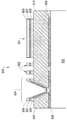
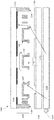
도 5는 셔터-기반 광 변조기들(셔터 어셈블리들)(502)을 포함하는 디스플레이 장치(500)의 예시적인 단면도를 도시한다. 각각의 셔터 어셈블리는 셔터(503) 및 앵커(505)를 포함한다. 앵커들(505)과 셔터들(503) 사이에 접속된 경우, 표면 위에서 짧은 거리로 셔터들을 서스펜딩시키는 것을 돕는 컴플리안트 빔 액츄에이터들은 도시되지 않는다. 셔터 어셈블리들(502)은 투명 기판(504) 상에 배치되며, 바람직하게는 플라스틱 또는 유리로 제조된다. 기판(504) 상에 배치된 후면-대면 반사성 어퍼쳐 층(506)은, 셔터 어셈블리들(502)의 셔터들(503)의 폐쇄 포지션들 아래에 로케이팅된 복수의 표면 어퍼쳐들(508)을 정의한다. 반사성 어퍼쳐 층(506)은, 표면 어퍼쳐들(508)을 관통하지 않는 광을, 디스플레이 어퍼쳐(500)의 후면을 향해 역으로 반사시킨다. 반사성 어퍼쳐 층(506)은, 스퍼터링, 증발, 이온 도금, 레이저 어블레이션(laser ablation), 또는 화학 기상 증착을 포함하는 다수의 기상 증착 기술들에 의해 박막 방식으로 형성된 포함물들 없는 미세(fine-grained) 금속막일 수 있다. 몇몇 구현들에서, 반사성 어퍼쳐 층(506)은, 유전체 미러와 같은 미러로부터 형성될 수 있다. 유전체 미러는, 높은 반사율과 낮은 반사율의 재료들 사이에서 교변하는 유전체 박막들의 스택으로서 제조될 수 있다. 셔터들(503)을 반사성 어퍼쳐 층(506)으로부터 분리시키는 수직 갭(gap)은 0.5 내지 10미크론의 범위에 있으며, 그 갭 내에서 셔터는 이동하기에 자유롭다. 바람직하게, 수직 갭의 크기는 폐쇄 상태에서 어퍼쳐들(508)의 에지와 셔터들(503)의 에지 사이의 (도 4b에 도시된 중첩부(416)와 같은) 측면 중첩부보다 작다.Figure 5 illustrates an exemplary cross-sectional view of a
디스플레이 장치(500)는, 기판(504)을 평면형 광 가이드(516)로부터 분리시키는 선택적인 디퓨져(diffuser) 및/또는 선택적인 밝기 향상 막(514)을 포함한다. 광 가이드는, 투명한, 즉 유리 또는 플라스틱 재료를 포함한다. 광 가이드(516)는 하나 또는 그 초과의 광 소스들(518)에 의해 조명되고, 백라이트(515)를 형성한다. 광 소스들(518)은, 예를 들어 그리고 제한 없이, 백열 램프들, 형광 램프들, 레이저들 또는 발광 다이오드(LED)들(일반적으로, "램프들"로 지칭됨)일 수 있다. 반사기(519)는, 광 소스(518)로부터의 광을 광 가이드(516)를 향해 지향시키는 것을 돕는다. 전면-대면 반사성 막(520)은 백라이트(515) 뒤에 배치되며, 광을 셔터 어셈블리들(502)을 향해 반사시킨다. 셔터 어셈블리들(502) 중 하나를 관통하지 않는 백라이트(515)로부터의 레이(ray)(521)와 같은 광 레이들은, 백라이트(515)로 리턴되고, 막(520)으로부터 다시 반사될 것이다. 이러한 방식으로, 제 1 경로 상에서 이미지를 형성하기 위해 디스플레이를 떠나기를 실패한 광은 재활용(recycle)될 수 있으며, 셔터 어셈블리들(502)의 어레이 내의 다른 개방 어퍼쳐들을 통한 투과를 위해 이용가능하게 될 수 있다. 그러한 광 재활용은 디스플레이의 조명 효율을 증가시키는 것으로 도시된다.The
광 가이드(516)는, 광 소스(518)로부터 어퍼쳐들(508)을 향해 및 그에 따라 디스플레이의 전면을 향해 광을 재지향시키는 기하학적 광 재지향기들 또는 프리즘들(517)의 세트를 포함한다. 광 재지향기들은, 대안적으로는 단면이 삼각형, 사다리꼴, 또는 만곡형일 수 있는 형상들을 갖는 광 가이드(516)의 플라스틱 몸체로 몰딩될 수 있다. 프리즘들(517)의 밀도는 일반적으로, 광 소스(518)로부터의 거리에 따라 증가한다.The light guide 516 includes a set of geometric light re-directors or
몇몇 구현들에서, 어퍼쳐 층(506)은 광 흡수 재료로 제조될 수 있으며, 대안적인 구현들에서, 셔터(503)의 표면들은 광 흡수 또는 광 반사 재료 중 어느 하나로 코팅될 수 있다. 몇몇 다른 구현들에서, 어퍼쳐 층(506)은 광 가이드(516)의 표면 상에 직접 증착될 수 있다. 몇몇 구현들에서, 어퍼쳐 층(506)은 (후술되는 MEMS-다운(down) 구성에서와 같이) 셔터들(503) 및 앵커들(505)과 동일한 기판 상에 배치될 필요는 없다.In some implementations, the
몇몇 구현들에서, 광 소스(518)는 상이한 컬러들, 예를 들어, 컬러들 레드, 그린 및 블루의 램프들을 포함할 수 있다. 컬러 이미지는, 인간의 두뇌가 단일 멀티-컬러 이미지로 상이한 컬러 이미지들을 평균하기에 충분한 레이트로 상이한 컬러들의 램프들을 이용하여 이미지들을 순차적으로 조명함으로써 형성될 수 있다. 다양한 컬러-특정 이미지들은 셔터 어셈블리들(502)의 어레이를 사용하여 형성된다. 다른 구현에서, 광 소스(518)는 3개 초과의 상이한 컬러들을 갖는 램프들을 포함한다. 예를 들어, 광 소스(518)는 레드, 그린, 블루 및 화이트 램프들, 또는 레드, 그린 블루 및 엘로우 램프들을 가질 수도 있다. 몇몇 다른 구현들에서, 광 소스(518)는 시안(cyan), 마젠타(magenta), 엘로우 및 화이트 램프들, 레드, 그린, 블루 및 화이트 램프들을 포함할 수도 있다. 몇몇 다른 구현들에서, 부가적인 램프들이 광 소스에 포함될 수도 있다. 예를 들어, 5개의 컬러들을 사용하면, 광 소스는 레드, 그린, 블루, 시안 및 엘로우 램프들을 포함할 수도 있다. 몇몇 다른 구현들에서, 광 소스(518)는 화이트, 오렌지, 블루, 퍼플 및 그린 램프들 또는 화이트, 블루, 엘로우, 레드 및 시안 램프들을 포함할 수도 있다. 6개의 컬러들을 사용하면, 광 소스는 레드, 그린, 블루, 시안, 마젠타 및 엘로우 램프들 또는 화이트, 시안, 마젠타, 엘로우, 오렌지 및 그린 램프들을 포함할 수도 있다.In some implementations, the
커버 플레이트(522)는 디스플레이 장치(500)의 전면을 형성한다. 커버 플레이트(522)의 후면 측은 콘트라스트를 증가시키기 위해 블랙 매트릭스(524)로 커버될 수 있다. 대안적인 구현들에서, 커버 플레이트는 컬러 필터들, 예를 들어, 셔터 어셈블리들(502) 중 상이한 어셈블리들에 대응하는 별개의 레드, 그린, 및 블루 필터들을 포함한다. 커버 플레이트(522)는 셔터 어셈블리들(502)로부터 떨어진 미리 결정된 거리에서 지지되어, 갭(526)을 형성한다. 캡(526)은 기계적 지지부들 또는 스페이서들(527)에 의해 및/또는 기판(504)에 커버 플레이트(522)를 부착시키는 접착 씨일(adhesive seal)(528)에 의해 유지된다.The cover plate 522 forms the front surface of the
접착 씨일(528)은 유체(530)로 씨일된다. 유체(530)는, 바람직하게는 약 10 센티포아즈(centipoise) 아래의 점성들 및 바람직하게는 약 2.0의 비유전 상수, 및 약 104V/cm의 유전 파괴 강도들을 이용하여 엔지니어링된다. 유체(530)는 또한 윤활류로서 기능할 수 있다. 몇몇 구현들에서, 유체(530)는 높은 표면 습윤(wetting) 능력을 갖는 소수성 액체이다. 대안적인 구현들에서, 유체(530)는, 기판(504)의 반사율보다 크거나 작은 반사율을 갖는다.The
기계적 광 변조기들을 포함하는 디스플레이들은, 수백, 수천 또는 몇몇 경우들에서는 수백만의 이동성 엘리먼트들을 포함할 수 있다. 몇몇 디바이스들에서, 엘리먼트의 모든 각각의 이동은, 정지 마찰(static friction)이 엘리먼트들 중 하나 또는 그 초과를 디스에이블시키기 위한 기회를 제공한다. 이러한 이동은, 모든 부분들을 유체(또한 유체(530)로 지칭됨)에 침지시키고, MEMS 디스플레이 셀 내의 유체 공간 또는 갭 내에 유체를 (예를 들어, 접착제를 이용하여) 씨일링시킴으로써 용이하게 된다. 일반적으로, 유체(530)는, 장기적으로는 낮은 마찰 계수, 낮은 점성, 및 최소의 열화 효과들을 갖는 유체이다. MEMS-기반 디스플레이 어셈블리가 유체(530)에 대한 액체를 포함하는 경우, 액체는 MEMS-기반 광 변조기의 이동 부분들 중 몇몇을 적어도 부분적으로 둘러싼다. 몇몇 구현들에서, 액츄에이션 전압들을 감소시키기 위해, 액체는 70센티포아즈 아래의 점성을 갖는다. 몇몇 다른 구현들에서, 액체는 10센티포아즈 아래의 점성을 갖는다. 70센티포아즈 아래의 점성들을 갖는 액체들은, 낮은 몰 중량들, 즉 4000 그램/몰 아래, 또는 몇몇 경우들에서는 400 그램/몰 아래의 몰 중량들을 갖는 재료들을 포함할 수 있다. 그러한 구현들에 또한 적합할 수도 있는 유체들(530)은, 탈이온수, 메탄올, 에탄올 및 다른 알콜들, 파라핀들, 올레핀들, 에테르들, 실리콘 오일들, 플루오르화된 실리콘 오일들, 또는 다른 자연적인 또는 합성 솔벤트들 또는 윤활류들을 제한없이 포함한다. 유용한 유체들은, 헥사메틸디실록산 및 옥타메틸트리실록산과 같은 폴리디메틸실록산들(PDMS), 또는 헥실펜타메틸디실록산과 같은 알킬 메틸 실록산들일 수 있다. 유용한 유체들은 옥탄 또는 데칸과 같은 알칸들일 수 있다. 유용한 유체들은, 니트로메탄과 같은 니트로알칸들일 수 있다. 유용한 유체들은 톨루엔 또는 디에틸벤젠과 같은 방향족 화합물들일 수 있다. 유용한 유체들은, 부탄온 또는 메틸 이소부틸 케톤과 같은 케톤들일 수 있다. 유용한 유체들은 클로로벤젠과 같은 클로로카본들일 수 있다. 유용한 유체들은, 디클로로플루오르에탄 또는 클로로트리플루오르에틸렌과 같은 클로로플루오르카본들일 수 있다. 이들 디스플레이 어셈블리들에 대해 고려되는 다른 유체들은 부틸 아세테이트, 디메틸포름아미드를 포함한다. 이들 디스플레이들에 대한 또 다른 유용한 유체들은 하이드로 플루오르 에테르들, 퍼플루오르폴리에테르들, 하이드로 플루오르 폴리 에테르들, 펜타놀, 및 부탄놀을 포함한다. 예시적인 적절한 하이드로 플루오르 에테르들은 에틸 노나플루오르부틸 에테르 및 2-트리플루오르메틸-3-에톡시도데카플루오르헥산을 포함한다.Displays comprising mechanical optical modulators may include millions of mobility elements in hundreds, thousands or even in some cases. In some devices, every individual movement of the element provides an opportunity for static friction to disable one or more of the elements. This movement is facilitated by immersing all portions in a fluid (also referred to as fluid 530) and by curing fluid (e.g., using an adhesive) in a fluid space or gap within the MEMS display cell. Generally,
시트 금속 또는 몰딩된 플라스틱 어셈블리 브라켓(532)은, 커버 플레이트(522), 기판(504), 백라이트(515) 및 다른 컴포넌트 부분들을 에지들 주변에서 함께 홀딩한다. 어셈블리 브라켓(532)은, 결합된 디스플레이 장치(500)에 강직성을 부가하기 위해, 스크류들 또는 톱니(indent) 탭들을 이용하여 조여진다. 몇몇 구현들에서, 광 소스(518)는 에폭시 포팅(potting) 화합물에 의해 적소에서 몰딩된다. 반사기들(536)은, 광 가이드(516)의 에지들로부터 벗어나는 광을 역으로 광 가이드에 리턴시키는 것을 돕는다. 제어 신호들 뿐만 아니라 전력을 셔터 어셈블리들(502) 및 광 소스(518)에 제공하는 전기 상호접속부들이 도 5에 도시되지 않는다.The sheet metal or molded
디스플레이 장치(500)는 MEMS-업(up) 구성으로 지칭되며, 여기서, MEMS 기반 광 변조기들은 기판(504)의 전면 표면, 즉 뷰어를 향해 대면하는 표면 상에 형성된다. 셔터 어셈블리들(502)은 반사성 어퍼쳐 층(506)의 상단 상에 직접 구축된다. MEMS-다운 구성으로 지칭되는 대안적인 구현에서, 셔터 어셈블리들은, 반사성 어퍼쳐 층이 형성되는 기판으로부터 분리되어 기판 상에 배치된다. 반사성 어퍼쳐 층이 형성되어 복수의 어퍼쳐들을 정의하는 기판은 본 명세서에서 어퍼쳐 플레이트로 지칭된다. MEMS-다운 구성에서, MEMS-기반 광 변조기들을 보유하는 기판은 디스플레이 장치(500)에서 커버 플레이트(522)를 대체하며, MEMS-기반 광 변조기들이 상단 기판의 후면 표면, 즉 뷰어로부터 떨어지고 백 라이트(516)를 향해 대면하는 표면 상에 포지셔닝되도록 배향된다. 그에 의해, MEMS-기반 광 변조기들은, 반사성 어퍼쳐 층(506)으로부터의 갭에 직접 반대로 및 그 갭에 걸쳐 포지셔닝된다. 갭은, MEMS 변조기들이 형성되는 기판과 어퍼쳐 플레이트를 접속시키는 일련의 스페이서 포스트들에 의해 유지될 수 있다. 몇몇 구현들에서, 스페이서들은, 어레이 내의 각각의 픽셀 내에 또는 그 사이에 배치된다. MEMS 광 변조기들을 그들의 대응하는 어퍼쳐들로부터 분리시키는 갭 또는 거리는, 바람직하게 10미크론 미만이거나, 또는 셔터들과 어퍼쳐들 사이의 (중첩부(416)와 같은) 중첩부보다 작은 거리이다.The
도 6a-6e는, 예시적인 복합 셔터 어셈블리의 구성의 스테이지들의 단면도들을 도시한다. 도 6a는, 완료된 복합 셔터 어셈블리(600)의 예시적인 단면도를 도시한다. 셔터 어셈블리(600)는 셔터(601), 2개의 컴플리안트 빔들(602), 및 기판(603) 및 어퍼쳐 층(606) 상에 구축된 앵커 구조(604)를 포함한다. 복합 셔터 어셈블리(600)의 엘리먼트들은 제 1 기계적 층(605), 도전체 층(607), 제 2 기계적 층(609), 및 인캡슐레이팅(encapsulating) 유전체(611)를 포함한다. 기계적 층들(605 또는 609) 중 적어도 하나는 0.15 미크론을 초과하는 두께들로 증착될 수 있으므로, 기계적인 층들 중 하나 또는 둘 모두가 셔터 어셈블리에 대한 기본적인 로드 베어링 및 기계적인 액츄에이션 부재로서 기능하지만, 몇몇 구현들에서, 기계적인 층들(605 및 609)은 더 얇을 수도 있다. 기계적인 층들(605 및 609)에 대한 후보 재료들은, 알루미늄(Al), 구리(Cu), 니켈(Ni), 크롬(Cr), 몰리브덴(Mo), 티타늄(Ti), 탄탈륨(Ta), 니오븀(Nb), 네오디뮴(Nd), 또는 이들의 합금과 같은 금속들; 알루미늄 산화물(Al2O3), 실리콘 산화물(SiO2), 탄탈륨 5산화물(Ta2O5), 또는 실리콘 질화물(Si3N4)와 같은 유전체 재료들; 또는 다이아몬드-형 카본, 실리콘(Si), 게르마늄(Ge), 갈륨 비소화물(GaAs), 카드뮴 텔루르화물(CdTe) 또는 이들의 합금과 같은 반도전성 재료들을 제한없이 포함한다. 도전체 층(607)과 같은 층들 중 적어도 하나는, 액츄에이션 엘리먼트로 전하를 운반하고 액츄에이션 엘리먼트로부터 전하를 운반하기 위해 전기적으로 도전성이어야 한다. 후보 재료들은, Al, Cu, Ni, Cr, Mo, Ti, Ta, Nb, Nd, 또는 이들의 합금 또는 다이아몬드-형 카본, Si, Ge, GaAs, CdTe 또는 이들의 합금과 같은 반도전성 재료들을 제한없이 포함한다. 반도체 층들을 이용하는 몇몇 구현들에서, 반도체들은 인(P), 비소(As), 붕소(B), 또는 알루미늄(Al)과 같은 불순물들을 이용하여 도핑된다. 도 6a는, 유사한 두께들 및 기계적 속성들을 갖는 기계적 층들(605 및 609)이 도전체 층(607)의 어느 하나의 측면 상에 증착되는 복합물에 대한 샌드위치 구성을 도시한다. 몇몇 구현들에서, 샌드위치 구성은, 증착 이후 남아있는 스트레스들 및/또는 온도 변화들에 의해 부과된 스트레스들이 셔터 어셈블리(600)의 벤딩, 뒤틀림(warping) 또는 다른 변형을 야기하지 않을 것이라는 것을 보장하도록 돕는다.6A-6E illustrate cross-sectional views of stages of an exemplary composite shutter assembly configuration. FIG. 6A illustrates an exemplary cross-sectional view of a completed
몇몇 구현들에서, 복합 셔터 어셈블리(600) 내의 층들의 순서는 반전될 수 있어서, 셔터의 외부가 도전성 층으로부터 형성되지만, 셔터의 내부가 기계적 층으로부터 형성되게 한다.In some implementations, the order of the layers in the
셔터 어셈블리(600)는 인캡슐레이팅 유전체(611)를 포함할 수 있다. 몇몇 구현들에서, 유전체 코팅들은 컨포멀(conformal) 방식으로 적용될 수 있어서, 셔터들 및 빔들의 모든 하단, 상단들, 및 측면 표면들이 균일하게 코팅되게 한다. 그러한 박막들은, 열 산화에 의해 그리고/또는 알루미늄 산화물(Al2O3), 크롬(III) 산화물(Cr2O3), 티타늄 산화물(TiO2), 하프늄 산화물(HfO2), 바나듐 산화물(V2O5), 니오븀 산화물(Nb2O5), 탄탈륨 5산화물(Ta2O5), 실리콘 산화물(SiO2), 또는 실리콘 질화물(Si3N4)과 같은 절연체의 컨포멀 화학 기상 증착에 의해, 또는 원자층 증착을 통해 유사한 재료들을 증착시킴으로써 성장될 수 있다. 유전체 코팅 층은 10nm 내지 1미크론의 범위의 두께들로 도포될 수 있다. 몇몇 구현들에서, 스퍼터링 및 증발이 측벽들 상으로 유전체 코팅을 증착시키기 위해 사용될 수 있다.The
도 6b-6e는, 도 6에 도시된 셔터 어셈블리(600)를 형성하는데 사용되는 예시적인 프로세스의 특정한 중간 제조 단계들의 결과들의 예시적인 단면도들을 도시한다. 몇몇 구현들에서, 셔터 어셈블리(600)는, 도 3a 및 3b에 도시된 제어 매트릭스들과 같이, 박막 트랜지스터들의 액티브 매트릭스 어레이와 같은 이전에-존재하는 제어 매트릭스의 상단에 구축된다.6B-6E illustrate exemplary cross-sectional views of the results of certain intermediate manufacturing steps of an exemplary process used to form the
도 6b는 셔터 어셈블리(600)를 형성하는 예시적인 프로세스의 제 1 스테이지의 결과의 단면도를 도시한다. 도 6b에 도시된 바와 같이, 희생층(613)이 증착되고 패터닝된다. 몇몇 구현들에서, 폴리이미드가 희생 재료로서 사용된다. 다른 후보 희생 재료들은, 폴리아미드, 플루오르폴리머, 벤조사이클로부텐, 폴리페닐퀴녹실렌, 파릴렌, 또는 폴리노보넨과 같은 폴리머 재료들을 포함한다. 이들 재료들은, 거친 표면들을 평탄화시키고, 250C 를 초과하는 프로세싱 온도들에서 기계적 무결성(integrity)을 유지하기 위한 그들의 능력, 및 제거 동안 에칭 및/또는 열 분해의 그들의 용이성에 대해 선택된다. 다른 구현들에서, 희생층(613)은, 폴리비닐 아세테이트, 폴리비닐 에틸렌, 및 페놀 또는 노볼락 수지들과 같은 포토레지스트로부터 형성된다. 몇몇 구현들에서 사용되는 대안적인 희생층 재료는, 다른 전자 또는 구조 층들이 그의 제거를 위해 사용되는 플루오르수소산 용액들에 저항성이 있는 한, 우선적으로 제거될 수 있는 SiO2이다. 하나의 그러한 적절히 저항성있는 재료는 Si3N4이다. 다른 대안적인 희생층 재료는, 대부분의 금속들 및 Si3N4와 같이, 다른 전자 및 구조 층들이 그의 제거를 위해 사용되는 플루오린 플라즈마들 또는 제논 디플루오르(XeF2)에 저항성이 있는 한, 우선적으로 제거될 수 있는 Si이다. 또 다른 대안적인 희생층 재료는, 다른 전자 또는 구조 층들이 농축된 수산화나트륨(NaOH) 용액들과 같은 강염기 용액들에 저항성이 있는 한, 우선적으로 제거될 수 있는 Al이다. 적절한 재료들은, 예를 들어, Cr, Ni, Mo, Ta 및 Si를 포함한다. 또 다른 대안적인 희생층 재료는, 다른 전자 또는 구조 층들이 질산 또는 황산 용액들에 저항성이 있는 한, 우선적으로 제거될 수 있는 Cu이다. 그러한 재료들은, 예를 들어, Cr, Ni, 및 Si를 포함한다.6B shows a cross-sectional view of the results of the first stage of the exemplary process of forming the
다음으로, 희생층(613)은 앵커 영역들(604)에서 홀들 또는 비아들을 노출시키도록 패터닝된다. 희생층 재료로서 폴리이미드 또는 다른 비-광활성(non-photoactive) 재료들을 이용하는 구현들에서, 희생층 재료는, 즉, UV 포토마스크를 통해 노출되는 영역들이 현상액 용액에서 우선적으로 제거될 수 있게 하는 광활성제들을 포함하도록 포뮬레이팅(formulate)될 수 있다. 다른 재료들로부터 형성되는 희생층들은, 포토레지스트의 부가적인 층에 희생층(613)을 코팅하고, 포토레지스트를 포토패터닝하며, 최종적으로 에칭 마스크로서 포토레지스트를 사용함으로써 패터닝될 수 있다. 대안적으로, 희생층(613)은, SiO2 또는 Cr과 같은 금속의 박막일 수 있는 하드 마스크로 희생층을 코팅함으로써 패터닝될 수 있다. 그 후, 포토패턴은, 포토레지스트 및 습식 화학 에칭에 의해 하드 마스크로 전사된다. 하드 마스크에서 현상된 패턴은, 매우 깊고 협소한 앵커 홀들을 희생층(613)으로 전하는데 사용될 수 있는 건식 화학, 이방성, 또는 플라즈마 에칭 기술들에 매우 저항성이 있을 수 있다.Next, the
앵커 영역들(604)이 희생층(613)에서 개방된 이후, 노출된 하부 도전성 표면(614)은, 임의의 표면 산화물 층들을 제거하기 위해 화학적으로 또는 플라즈마의 스퍼터링 효과들을 통해 에칭될 수 있다. 그러한 콘택트(contact) 에칭 스테이지는, 기본 도전체와 셔터 재료 사이의 옴 콘택트를 개선시킬 수 있다. 희생층의 패터닝 이후, 임의의 포토레지스트 층들 또는 하드 마스크들은 솔벤트 세정들 또는 산성 에칭 중 어느 하나의 사용을 통해 제거될 수 있다.After the
다음으로, 도 6c에 도시된 바와 같이, 셔터 어셈블리(600)를 구축하기 위한 프로세스에서, 셔터 재료들이 증착된다. 셔터 어셈블리(600)는 다수의 박막들, 즉 제 1 기계적 층(605), 도전체 층(607) 및 제 2 기계적 층(609)으로 구성된다. 몇몇 구현들에서, 제 1 기계적 층(605)은 비정질 실리콘(a-Si) 층이고, 도전체 층(607)은 Al이며, 제 2 기계적 층(609)은 a-Si이다. 제 1 기계적 층(605), 도전체 층(607), 및 제 2 기계적 층(609)이 온도로 증착되며, 그 온도 아래에서, 물리적 열화가 희생층(613)에 대해 발생한다. 예를 들어, 폴리이미드는 400C 초과의 온도에서 분해된다. 따라서, 몇몇 구현들에서, 제 1 기계적 층(605), 도전체 층(607), 및 제 2 기계적 층(609)은 400C 아래의 온도들로 증착되며, 희생 재료로서 폴리이미드의 사용을 허용한다. 몇몇 구현들에서, 수소화된 비정질 실리콘(a-Si:H)은, 비교적 스트레스-없는 상태에서, 약 250 내지 350C의 범위 내의 온도들로 실란 가스로부터 플라즈마-보조 화학 기상 증착(PECVD)에 의해 그것이 약 0.15 내지 3미크론의 범위 내의 두께들로 성장될 수 있으므로, 제 1 및 제 2 기계적 층들(605 및 609)에 대한 유용한 기계적 재료이다. 그러한 구현들 중 몇몇에서, 포스핀 가스(PH3)는, a-Si가 약 1옴-cm 아래의 저항들로 성장될 수 있도록 도펀트로서 사용된다. 대안적인 구현들에서, 유사한 PECVD 기술은, 제 1 기계적 층(605)으로서 Si3N4, 실리콘-리치(silicon-rich) Si3N4, 또는 SiO2 재료들의 증착을 위해, 또는 제 1 기계적 층(605)에 대한 다이아몬드-형 카본, Ge, SiGe, CdTe, 또는 다른 반도전성 재료들의 증착을 위해 사용될 수 있다. PECVD 증착 기술의 이점은, 증착이 매우 콘포멀할 수 있다는 것이며, 즉, 그것은 다양한 경사진 표면들 또는 협소한 비아 홀들의 내부 표면들을 코팅할 수 있다는 것이다. 희생 재료로 절단되는 앵커 또는 비아 홀들이 매우 수직한 측벽들을 제시하더라도, PECVD 기술은, 앵커의 하단 및 상단 수평 표면들 사이에 연속적인 코팅을 제공할 수 있다.Next, as shown in FIG. 6C, in the process for constructing the
PECVD 기술에 부가하여, 제 1 및 제 2 기계적 층들(605 및 609)의 성장에 이용가능한 대안적인 적절한 기술들은, RF 또는 DC 스퍼터링, 금속-유기 화학 기상 증착, 증발, 전기도금 또는 무전해 도금을 포함한다.In addition to the PECVD technique, alternative suitable techniques that may be used to grow the first and second
도전성 층(607)에 대해, 몇몇 구현들에서, Al과 같은 금속 박막이 이용된다. 몇몇 다른 구현들에서, Cu, Ni, Mo, 또는 Ta와 같은 대안적인 금속들이 선택될 수 있다. 그러한 도전성 재료의 포함물은 2개의 목적들을 제공한다. 그것은, 셔터(601)의 전체 시트 저항을 감소시키며, 그것은, 셔터의 몇몇 구현들에서 사용될 수도 있는 바와 같은 a-Si가 두께가 2미크론 미만이면, 몇몇 정도로 가시 광을 송신할 수 있으므로, 셔터(601)를 통한 가시 광의 전달을 차단하도록 돕는다. 도전성 재료는, 스퍼터링 또는 더 컨포멀한 방식으로는 화학 기상 증착 기술들, 전기도금, 또는 무전해 도금에 의해 증착될 수 있다.For the
도 6d는 셔터 어셈블리(600)의 형성에서 사용되는 프로세싱 스테이지들의 다음의 세트의 결과들을 도시한다. 제 1 기계적 층(605), 도전성 층(607), 및 제 2 기계적 층(609)은, 희생층(613)이 기판(603) 상에 여전히 존재하는 동안 포토마스킹되고 에칭된다. 먼저, 포토레지스트 재료가 도포되고, 그 후, 포토마스크를 통해 노출되며, 그 후, 에칭 마스크를 형성하도록 현상된다. 그 후, 비정질 실리콘, Si3N4 및 SiO는 플루오린-기반 플라즈마 케미스트리(chemistry)들에서 에칭될 수 있다. SiO2 기계적 층들은 HF 습식 화학물들을 사용하여 에칭될 수 있으며; 도전성 층(607) 내의 임의의 금속들은 습식 화학물들 또는 염소-기반 플라즈마 케미스트리들 중 어느 하나를 이용하여 에칭될 수 있다.6D shows the results of the next set of processing stages used in the formation of the
포토마스크를 통해 도포된 패턴 형상들은, 셔터 어셈블리(600)의 액츄에이터 및 셔터(601)에서의 견고함, 컴플라이언스(compliance), 및 전압 응답과 같은 기계적 속성들에 영향을 준다. 셔터 어셈블리(600)는, 단면으로 도시된 컴플리안트 빔(602)을 포함한다. 컴플리안트 빔(602)은, 폭이 셔터 재료의 총 높이 또는 두께보다 작도록 형상화된다. 몇몇 구현들에서, 빔 치수 비율은 1.4:1 또는 그 초과로 유지되며, 컴플리안트 빔들(602)은 그들이 넓은(wide) 것보다 더 크고 더 두껍다.Pattern shapes applied through the photomask affect mechanical properties such as firmness, compliance, and voltage response at the actuator and shutter 601 of the
셔터 어셈블리(600)를 구축하기 위한 예시적인 제조 프로세스의 후속 스테이지들의 결과들은 도 6e에 도시된다. 희생층(613)이 제거되며, 이는, 앵커 포인트들을 제외하고 기판(603)으로부터 모든 이동 부분들을 자유롭게 한다(free-up). 몇몇 구현들에서, 폴리이미드 희생 재료들이 산소 플라즈마로 제거된다. 희생층(613)에 대해 사용되는 다른 폴리머 재료들은 또한, 산소 플라즈마로 또는 몇몇 경우들에서는 열분해(thermal pyrolysis)에 의해 제거될 수 있다. (SiO2와 같은) 몇몇 희생층 재료들은 습식 화학 에칭 또는 기체상 에칭에 의해 제거될 수 있다.The results of the subsequent stages of the exemplary fabrication process for building the
최종 프로세스에서, 결과들이 도 6a에 도시되며, 인캡슐레이팅 유전체(611)가 셔터(601)의 모든 노출된 표면들 상에 증착된다. 몇몇 구현들에서, 인캡슐레이팅 유전체(611)는, 셔터(601) 및 빔들(602)의 모든 하단, 상단들, 및 측면 표면들이 화학 기상 증착을 사용하여 균일하게 코팅되도록 콘포멀 방식으로 도포될 수 있다. 몇몇 다른 구현들에서, Al2O3는 인캡슐레이팅 유전체(611)에 대해 사용되며, 10 내지 100 나노미터의 범위 내의 두께들로 원자층 증착에 의해 증착된다.In the final process, the results are shown in FIG. 6A, and an encapsulating
최종적으로, 점착-방지(anti-stiction) 코팅들이 셔터(601) 및 빔들(602)의 표면들에 적용될 수 있다. 이들 코팅들은, 액츄에이터의 2개의 독립적인 빔들 사이에서 원치않는 부착 또는 접착을 방지한다. 적절한 코팅들은 카본 막들(흑연 및 다이아몬드-형 둘 모두) 뿐만 아니라 플루오르폴리머들, 및/또는 낮은 기압 윤활유들 뿐만 아니라 클로로실란들, 하이드로카본 클로로실란들, 플루오르카본 클로로실란들, 예컨대 메톡시-종단된 실란들, 퍼플루오르화된, 아미노-실란들, 실록산들 및 카본크실릴산계 모노머들 및 종들을 포함한다. 이들 코팅들은, 분자형 기상으로의 노출에 의해 또는 화학 기상 증착에 의한 전구체 화합물들의 분해에 의해 적용될 수 있다. 부착-방지 코팅들은 또한, 셔터 표면들의 화학적 변화에 의해, 예컨대 절연 표면들의 플루오르첨가(fluoridation), 실란처리(silanization), 실록시데이션(siloxidation), 또는 수소첨가(hydrogenation)에 의해 생성될 수 있다.Finally, anti-stiction coatings may be applied to the surfaces of the
MEMS-기반 셔터 디스플레이들에서의 사용을 위한 적절한 액츄에이터들의 하나의 클래스는, 디스플레이 기판에 대해 횡단하거나 디스플레이 기판의 평면 내에 있는 셔터 모션을 제어하기 위한 컴플리안트 액츄에이터 빔들을 포함한다. 그러한 셔터 어셈블리들의 액츄에이션을 위해 이용되는 전압은, 액츄에이터 빔들이 더 컴플리안트됨에 따라 감소한다. 평면 내 모션이 평면외 모션에 비해 우선되거나 촉진되도록 빔들이 형상화되면, 액츄에이팅된 모션의 제어가 또한 개선된다. 따라서, 몇몇 구현들에서, 컴플리안트 액츄에이터 빔들은 직사각형 단면을 가져서, 그 빔들이 넓은(wide) 것보다 그 빔들이 더 크고 더 두껍게 한다.One class of suitable actuators for use in MEMS-based shutter displays include compliant actuator beams for controlling shutter motion across a display substrate or within the plane of a display substrate. The voltage used for actuation of such shutter assemblies decreases as the actuator beams are more complicated. If the beams are shaped such that the in-plane motion is prioritized or facilitated relative to out-of-plane motion, the control of the actuated motion is also improved. Thus, in some implementations, the compliant actuator beams have a rectangular cross section, making the beams larger and thicker than their beams wide.
특정한 평면 내의 벤딩에 대한 긴 직사각형 빔의 견고성은, 그 평면 내의 그 빔의 가장 얇은 치수를 이용하여 제 3 전력으로 스캐일링(scale)된다. 따라서, 평면내 모션에 대한 액츄에이션 전압들을 감소시키기 위해 컴플리안트 빔들의 폭을 감소시키는 것이 유리하다. 그러나, 셔터 및 액츄에이터 구조들을 정의 및 제조하기 위해 종래의 포토리소그래피 장비를 사용하는 경우, 빔들의 최소 폭은 옵틱스들의 해상도로 제한될 수 있다. 그리고, 포토리소그래피 장비가 15나노미터만큼 협소한 피쳐들로 포토레지스트에 패턴들을 정의하기 위해 현상되지만, 그러한 장비는 비싸며, 패터닝이 단일 노출로 달성될 수 있는 영역들은 제한된다. 큰 유리 패너들에 대한 경제적인 포토리소그래피에 대해, 패터닝 해상도 또는 최소 피쳐 사이즈는 통상적으로 1미크론 또는 2미크론 또는 그 초과로 제한된다.The robustness of a long rectangular beam for bending in a particular plane is scaled to a third power using the thinnest dimension of that beam in its plane. It is therefore advantageous to reduce the width of the compliant beams to reduce actuation voltages for in-plane motion. However, if conventional photolithographic equipment is used to define and fabricate shutter and actuator structures, the minimum width of the beams can be limited to the resolution of the optics. And while photolithography equipment is developed to define patterns in photoresist with features as narrow as 15 nanometers, such equipment is expensive and the areas in which patterning can be achieved with a single exposure are limited. For economical photolithography for large glass panes, the patterning resolution or minimum feature size is typically limited to 1 micron or 2 microns or more.
도 7a-7d는, 협소한 측벽 빔들을 갖는 예시적인 셔터 어셈블리(700)의 구성의 스테이지들의 등척도들을 도시한다. 이러한 대안적인 프로세스는, 컴플리안트 액츄에이터 빔들(718 및 720) 및 컴플리안트 스프링 빔(716)(집합적으로, "측벽 빔들(716, 718, 및 720)"로 지칭됨)을 산출하며, 이들은 큰 유리 패널들에 대한 종래의 리소그래피 제한들 훨씬 아래에 있는 폭을 갖는다. 도 7a-7d에 도시된 프로세스에서, 셔터 어셈블리(700)의 컴플리안트 빔들은 희생 재료로부터 재조된 몰드 상에 측벽 피쳐들로서 형성된다. 프로세스는 측벽 빔 프로세스로 지칭된다.7A-7D illustrate isometric views of the stages of the construction of an
측벽 빔들(716, 718, 및 720)을 갖는 셔터 어셈블리(700)를 형성하는 프로세스는 도 7a에 도시된 바와 같이, 제 1 희생 재료(701)의 증착 및 패터닝으로 시작한다. 제 1 희생 재료에 정의된 패턴은 개구들 또는 비아들(702)을 생성하며, 그들 내에서 셔터에 대한 앵커들이 결국 형성될 것이다. 제 1 희생 재료(701)의 증착 및 패터닝은, 도 6a-6e와 관련하여 설명된 증착 및 패터닝에 대하여 설명된 것들과 개념적으로 유사하며, 유사한 재료들을 사용한다.The process of forming the
측벽 빔들(716, 718 및 720)을 형성하는 프로세스는, 제 2 희생 재료(705)의 증착 및 패터닝으로 계속된다. 도 7b는, 제 2 희생 재료(705)의 패터닝 이후 생성되는 몰드(703)의 형상을 도시한다. 몰드(703)는 또한, 자신의 이전에 정의된 비아들(702)을 갖는 제 1 희생 재료(701)를 포함한다. 도 7b의 몰드(703)는 2개의 별개의 수평 레벨들을 포함하며; 몰드(703)의 하단 수평 레벨(708)은 제 1 희생층(701)의 상단 표면에 의해 설정되며, 제 2 희생층(705)이 에칭되어 떨어지는(etch away) 그들 영역들에스 액세스가능하다. 몰드(703)의 상단 수평 레벨(710)은 제 2 희생층(705)의 상단 표면에 의해 설정된다. 도 7b에 도시된 몰드(703)는 또한, 실질적으로 수직인 측벽들(709)을 포함한다.The process of forming the side wall beams 716, 718, and 720 continues with the deposition and patterning of the second
제 1 및 제 2 희생층들(701 및 705)로서의 사용을 위한 재료들은 도 6a-6e의 희생층(613)에 대해 상술된다.Materials for use as the first and second
측벽 빔들(716, 718 및 720)을 형성하는 프로세스는, 도 7c에 도시된 바와 같이, 몰드(703)의 노출된 표면들 모두 상으로의 셔터 재료의 증착 및 패터닝으로 계속된다. 셔터(712)를 형성할 시에 사용을 위한 적절한 재료들은, 도 6a-6e의 제 1 기계적 층(605), 도전성 층(607), 및 제 2 기계적 층(609)에 대해 상술된다. 셔터 재료는, 약 2미크론 미만의 두께로 증착된다. 몇몇 구현들에서, 셔터 재료는 약 1.5미크론 미만의 두께를 갖도록 증착된다. 몇몇 다른 구현들에서, 셔터 재료는, 약 1.0미크론 미만 및 약 0.10미크론 만큼 얇은 두께를 갖도록 증착된다. 증착 이후, (상술된 바와 같이 수 개의 재료들의 복합물일 수도 있는) 셔터 재료는 도 7c에 도시된 바와 같이 패터닝된다. 먼저, 포토레지스트 마스크가 셔터 재료 상에 증착된다. 그 후, 포토레지스트가 패터닝된다. 후속 에칭 스테이지 이후, 셔터 재료가 셔터(712) 뿐만 아니라 앵커들(714)의 영역에 남아있도록, 포토레지스트로 현상되는 패턴이 설계된다.The process of forming the side wall beams 716, 718 and 720 continues with the deposition and patterning of the shutter material onto all of the exposed surfaces of the
제조 프로세스는 이방성 에칭을 적용하는 것으로 계속되며, 도 7c에 도시된 구조를 초래한다. 셔터 재료의 이방성 에칭은, 기판 또는 기판에 근접한 전극에 인가된 전압 바이어스를 이용하여 플라즈마 분위기에서 수행된다. (기판의 표면에 수직한 전기장을 갖는) 바이어싱된 기판은, 기판에 거의 수직한 각도로 기판을 향한 이온들의 가속화를 유도한다. 에칭 화학물들과 커플링된 그러한 가속된 이온들은, 기판에 평행한 방향들과 비교하여 기판의 평면에 수직한 방향에서 훨씬 더 신속한 에칭 레이트들을 유도한다. 그에 의해, 포토레지스트에 의해 보호된 영역들 내의 셔터 재료의 언더컷(undercut)-에칭이 실질적으로 제거된다. 가속된 이온들의 트랙과 실질적으로 평행한 몰드(703)의 측벽 표면들(709)에 따라, 셔터 재료는 또한 이방성 에칭으로부터 실질적으로 보호된다. 그러한 보호된 측벽 셔터 재료는 셔터(712)를 지지하기 위한 측벽 빔들(716, 718 및 720)을 형성한다. 상단 수평 표면(710) 또는 하단 수평 표면(708)과 같은 몰드의 다른(비-포토레지스트-보호된) 수평 표면들에 따라, 셔터 재료는 에칭에 의해 완전히 제거된다.The fabrication process continues with the application of an anisotropic etch, resulting in the structure shown in Figure 7C. Anisotropic etching of the shutter material is performed in a plasma atmosphere using a voltage bias applied to the substrate or the electrode proximate to the substrate. A biased substrate (having an electric field perpendicular to the surface of the substrate) induces acceleration of ions toward the substrate at an angle substantially perpendicular to the substrate. Such accelerated ions coupled with etching chemistries induce much faster etch rates in directions perpendicular to the plane of the substrate as compared to directions parallel to the substrate. Thereby, the undercut-etching of the shutter material in the regions protected by the photoresist is substantially eliminated. Along the sidewall surfaces 709 of the
측벽 빔들(716, 718 및 720)을 형성하는데 사용되는 이방성 에칭은, 기판 또는 기판에 근접한 전극의 전기 바이어스에 대한 제공이 공급되는 한, RF 또는 DC 플라즈마 에칭 디바이스 중 어느 하나로 달성될 수 있다. RF 플라즈마 에칭의 경우에 대해, 동등한 자체-바이어스는, 여기 회로의 접지 플레이트들로부터 기판 홀더를 접속해제시키고, 그에 의해, 기판 전위가 플라즈마에서 플로팅(float)하게 함으로써 획득될 수 있다. 몇몇 구현들에서, 트리플루오르메탄(CHF3), 퍼플루오르부탄(C4F8), 또는 클로로폼(CHCl3)과 같은 에칭 가스를 제공하는 것이 가능하며, 여기서, 카본 및 수소 및/또는 카본 및 플루오린 둘 모두는 에칭 가스의 구성물들이다. 기판의 전압 바이어싱을 통해 다시 달성되는 방향성 플라즈마와 커플링되는 경우, 해방된 카본(C), 수소(H), 및/또는 플루오린(F) 원자들은 측벽들(709)로 이주할 수 있으며, 여기서, 그들은 패시브 또는 보호성 준-폴리머(quasi-polymer) 코팅을 구축한다. 이러한 준-폴리머 코팅은 추가적으로, 에칭 또는 화학적 공격으로부터 측벽 빔들(716, 718 및 720)을 보호한다.The anisotropic etching used to form the side wall beams 716, 718, and 720 can be achieved with either RF or DC plasma etching devices, provided that the provision of electrical bias for the substrate or electrodes proximate the substrate is provided. For the case of RF plasma etching, the equivalent self-bias can be obtained by disconnecting the substrate holder from the ground plates of the excitation circuit, thereby causing the substrate potential to float in the plasma. In some implementations it is possible to provide an etching gas such as trifluoromethane (CHF 3 ), perfluorobutane (C 4 F 8 ), or chloroform (CHCl 3 ), wherein the carbon and hydrogen and / or carbon And fluorine are both constituents of the etching gas. The liberated carbon (C), hydrogen (H), and / or fluorine (F) atoms can migrate to the
측벽 빔들을 형성하는 프로세스는, 제 2 희생층(705) 및 제 1 희생층(701)의 나머지의 제거로 완료된다. 결과가 도 7d에 도시된다. 희생 재료를 제거하는 프로세스는, 도 6e에 대해 설명된 것과 유사하다. 몰드(703)의 측벽들(709) 상에 증착된 재료는 측벽 빔들(716, 718 및 720)로서 남아있다. 측벽 빔(716)은, 셔터(712)에 앵커들(714)을 기계적으로 접속시키며, 컴플리안트 빔들(718 및 720)로부터 형성된 액츄에이터에 의해 인가된 힘들에 대항하기 위해 패시브 회복력을 제공하는 스프링으로서 기능한다. 앵커들은 어퍼쳐 층(725)에 접속한다. 측벽 빔들(716, 718 및 720)은 크고 협소하다. 몰드(703)의 표면으로부터 형성된 바와 같은 측벽 빔들(716, 718 및 720)의 폭은, 증착된 바와 같은 셔터 재료의 두께와 유사하다. 몇몇 구현들에서, 측벽 빔(716)의 폭은 셔터(712)의 두께와 동일할 것이다. 다른 구현들에서, 빔 폭은 셔터(712)의 두께의 단지 약 1/2일 것이다. 측벽 빔들(716, 718 및 720)의 높이는, 제 2 희생 재료(705)의 두께에 의해, 즉, 도 7b에 관련하여 설명된 패터닝 단계 동안 생성된 바와 같은 몰드(703)의 깊이에 의해 결정된다. 증착된 셔터 재료의 두께가 2미크론 미만이도록 선택되는 한, 도 7a-7d에 도시된 방법은 매우 협소한 빔들의 제조에 매우 적합하다. 사실, 많은 애플리케이션들에 대해, 0.1 내지 2.0의 두께 범위는 매우 적절하다. 종래의 포토리소그래피는 도 7a, 7b 및 7c에 도시된 패터닝된 피쳐들을 훨씬 더 큰 치수들로 제한할 것이며, 예를 들어, 2미크론 또는 5미크론보다 작지 않은 최소의 분해된 피쳐들을 허용한다.The process of forming the sidewall beams is completed by the removal of the second
도 7d는, 상술된 프로세스에서 릴리즈 단계 이후 형성되며, 높은 애스팩트비(aspect ratio)를 이용하여 컴플리안트 빔들을 산출하는 셔터 어셈블리(700)의 등척도를 도시한다. 제 2 희생층의 두께가, 예를 들어, 셔터 재료의 두께보다 4배 더 큰 것보다 더 크게 되는 한, 빔 높이 대 빔 폭의 결과적인 비율은 유사한 비율, 즉 4:1보다 크게 제조될 것이다.7D shows an isometric view of the
상기 도시되지는 않았지만 도 7c로 유도되는 프로세스의 일부로서 포함되는 선택적인 스테이지는, 컴플리안트 드라이브 빔들(718)로부터 컴플리안트 로드 빔들(720)을 분리 또는 디커플링시키기 위한 측벽 빔 재료의 등방성 에칭을 수반한다. 예를 들어, 포인트(724)에서의 셔터 재료는 등방성 에칭의 사용을 통해 측벽으로부터 제거된다. 등방성 에칭은, 그의 에칭 레이트가 모든 방향들에서 동일하므로, 포인트(724)와 같은 영역들 내의 측벽 재료가 더 이상 보호되지 않는 에칭이다. 등방성 에칭은, 바이어스 전압이 기판에 인가되지 않는 한, 통상적인 플라즈마 에칭 장비에서 달성될 수 있다. 등방성 에칭은 또한, 습식 화학 또는 기체상 에칭 기술들을 사용하여 달성될 수 있다. 이러한 선택적인 제 4 마스킹 및 에칭 스테이지 이전에, 측벽 빔 재료는, 몰드(703) 내의 리세스(recess)된 피쳐들의 주변 주위에 본질적으로 계속 존재한다. 제 4 마스크 및 에칭 스테이지는, 측벽 재료를 분리 및 분할시키는데 사용되며, 별개의 빔들(718 및 720)을 형성한다. 포인트(724)에서의 빔들의 분리는, 포토레지스트 분배의 제 4 프로세스, 및 마스크를 통한 노출을 통해 달성된다. 이러한 경우, 포토레지스트 패턴은, 분리 포인트(724)를 제외하고 모든 포인트들에서 등방성 에칭에 대해 측벽 빔 재료를 보호하도록 설계된다.An optional stage, not shown here as part of the process induced by Figure 7C, is an isotropic etch of sidewall beam material for separating or decoupling the compliant load beams 720 from the compliant drive beams 718 Lt; / RTI > For example, the shutter material at
측벽 프로세스의 최종 스테이지로서, 인캡슐레이팅 유전체가 측벽 빔들의 외부 표면들 주위에 증착된다.As a final stage of the sidewall process, an encapsulating dielectric is deposited around the outer surfaces of the side wall beams.
몰드(703)의 측벽들(709) 상에 증착된 셔터 재료를 보호하고, 실질적으로 균일한 단면의 측벽 빔들(716, 718 및 720)을 생성하기 위해, 몇몇 특정한 프로세스 가이드라인들이 후속될 수 있다. 예를 들어, 도 7b에서, 측벽들(709)은 가능한 수직하게 제조될 수 있다. 측벽들(709) 및/또는 노출된 표면들에서의 기울기(slope)들은 이방성 에칭에 민감하게 된다. 몇몇 구현들에서, 수직 측벽들(709)은 도 7b의 패터닝 단계, 즉 이방성 방식의 제 2 희생 재료(705)의 패터닝에 의해 제조될 수 있다. 제 2 희생층(705)의 패터닝과 함께 부가적인 포토레지스트 코팅 또는 하드마스크의 사용은, 포토레지스트의 과도한 마모의 두려움 없이 제 2 희생 재료(705)의 이방성 에칭에서 어그레시브(aggressive)한 플라즈마들 및/또는 높은 기판 바이어스들을 이용하는 것을 가능하게 한다. 수직 측벽들(709)은 또한, UV 노출 동안 포커스의 깊이를 제어하기 위한 주의가 취해지고 과도한 수축이 레지스트의 최종 경화 동안 회피되는 한, 포토이미징가능한 희생 재료에서 제조될 수 있다.Some specific process guidelines may be followed to protect the shutter material deposited on the
측벽 빔 프로세싱 동안 도움이 되는 다른 프로세스 규격은, 셔터 재료 증착의 콘포멀러티(conformality)에 관련된다. 바람직하게, 몰드(703)의 표면들은, 그들 표면들의 배향에 관계없이, 즉 수직이던 수평이던 유사한 두께의 셔터 재료로 커버된다. 그러한 콘포멀러티는, 화학 기상 증착 기술(CVD)을 이용하여 증착하는 경우 달성될 수 있다. 특히, 다음의 콘포멀 기술들, 즉 플라즈마 향상된 화학 기상 증착(PECVD), 낮은 압력 화학 기상 증착(LPCVD), 및 원자 또는 자체-제한된 층 증착(ALD)이 이용될 수 있다. 상기 CVD 기술들에서, 박막의 성장 레이트는, 소스 원자들의 방향성 플럭스에 기판을 노출시키는 것과는 대조적으로 기판 상의 반응 레이트들에 의해 제한될 수 있다. 몇몇 구현들에서, 수직 표면들 상에서 성장되는 재료의 두께는 수평 표면들 상에서 성장되는 재료의 두께의 적어도 50%이다. 대안적으로, 셔터 재료들은, 도금 이전에 표면들을 코팅하는 금속 시드층이 제공된 이후, 무전해 도금 또는 전기 도금에 의해 용액으로부터 컨포멀하게 증착될 수 있다.Other process specifications that aid during sidewall beam processing relate to the conformality of shutter material deposition. Preferably, the surfaces of the
도 7d의 셔터 어셈블리(700)를 유도하는 프로세스는 4-마스크 프로세스이며, 이는, 포토-민감형 폴리머가 포토마스크를 통해 원하는 패턴을 조명함으로써 노출되는 프로세스 포함된 4개의 별개의 포토리소그래피 스테이지들을 의미한다. 마스킹 단계들로서 또한 알려진 포토리소그래피 스테이지들은 MEMS 디바이스들의 제조에서 가장 비싼 것 중 하나이므로, 감소된 수의 마스킹 단계들로 제조 프로세스를 생성하는 것이 바람직하다.The process of deriving the
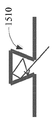
도 8은 루프된 드라이브 빔을 포함하는 셔터 어셈블리(802)의 평면도를 도시한다. 루프된 드라이브 빔은 듀얼 컴플리안트 액츄에이터 어셈블리(854)의 일부를 형성한다. 듀얼 컴플리안트 액츄에이터 어셈블리(854)는, 도 4a 및 4b의 셔터 어셈블리(400)에 대해 설계된 액츄에이터(404)와 유사하게 기능한다. 액츄에이터 어셈블리(854)는 컴플리안트 로드 빔들(858 및 859)과 함께 컴플리안트 드라이브 빔들(856 및 857)을 포함한다. 로드 빔들(858 및 859)은 일 단부 상에 셔터(860)를 지지하며, 다른 단부에서 로드 빔 앵커들(862 및 863)에 각각 부착된다. 드라이브 빔들(856 및 857)은 루프로서 형상화된다. 드라이브 빔들(856 및 857)의 각각의 단부는 공통 앵커(864)에 부착된다. 루프를 따라, 동일한 빔의 리턴 섹션에 실질적으로 평행한 아웃고잉 빔의 섹션이 존재한다. 이들 2개의 루프 섹션들의 길이들은 동일하다. 측벽 빔 프로세스에서 형성되는 경우, 드라이브 빔들(856 및 857)의 아웃고잉 섹션을 변형시키는 경향이 있을 스트레스들은, 빔의 리턴 섹션을 따라 스트레스들을 미러링하거나 대항할 것이다.FIG. 8 shows a top view of a shutter assembly 802 including a looped drive beam. The looped drive beam forms part of dual
드라이브 빔들(856 및 857)을 구성하는 컴플리안트 빔들은, 도 7a-7d에 도시된 셔터 어셈블리(700)에 대해 설명된 첫번째 3개의 마스크 스테이지들만을 사용하여 완전하게 정의될 수 있다. 드라이브 빔이 로드 빔으로부터 분리되는 4번째 포토-리소그래피 스테이지는, 빔들(856 및 857)을 제조하는데 사용되지 않는다. 루프들은 공간의 경계 주위의 주변부를 완전히 에워싸거나 형성한다. (에워싸인 공간 주위의 경계에 대해 예상되는 바와 같이) 루프들에서 어떠한 종단도 존재하지 않으므로, 4번째 포토-리소그래피 스테이지가 요구되지 않는다.The compliant beams that make up the drive beams 856 and 857 can be fully defined using only the first three mask stages described for the
4번째 마스크를 완전히 제거하기 위해, 방법이 추구되며, 그에 의해, 구조 내의 다른 컴플리안트 빔들이 루프들과 유사한 형상들을 포함하도록 제조된다. 측벽 빔의 종단은, 공간을 완전히 에워싸는 경계를 빔이 형성하는 한 필요하지 않다. 셔터 어셈블리(852) 내의 로드 빔(858)은 로드 빔 앵커(862)에서 종단되므로, 이러한 구현에서, 4번째 마스킹 스테이지는 앵커(862)에서 빔(858)을 종결시키는데 사용된다.To completely remove the fourth mask, a method is pursued whereby other compliant beams within the structure are fabricated to include loops and similar shapes. The end of the side wall beam is not necessary as long as the beam forms a boundary that completely surrounds the space. The
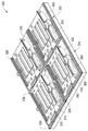
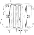
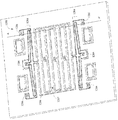
도 9는 3-마스크 프로세스에 따라 구축된 셔터 어셈블리(900)의 등척도를 도시한다. 즉, 셔터 어셈블리(900)는 3개의 마스킹 단계들만을 사용하여 제조될 수 있다. 그들 3개의 마스킹 단계들은, 제 1 희생층, 제 2 희생층, 및 셔터 재료로 패턴들을 현상하기 위해 각각 사용되는 앵커 정의 단계, 몰드 정의 단계, 및 셔터 정의 단계로 지칭된다. 셔터 어셈블리(700)에 대해 설명된 바와 같이, 컴플리안트 빔들은 몰드의 측벽들에서 형성되며, 또한 제 2 희생층으로 지칭된다. 셔터 어셈블리(900)는, 몰드 내의 피쳐들의 주변을 에워싸는 폐쇄된 경계들로서 빔들이 설계되기 때문에, 3-마스크 프로세스를 사용하여 제조될 수 있다.Figure 9 shows an isometric view of a
셔터 어셈블리(900)는 셔터(902), 강성(stiffening) 립들(903), 로드 빔들(904), 로드 빔 앵커들(906), 드라이브 빔들(908), 및 드라이브 빔 앵커들(910)을 포함한다. 드라이브 빔들(908)은 루프로 형성되며, 앵커(910)에서 기판에 부착된다. 드라이브 빔들(908)은 루프 내의 공간을 에워싼다. 셔터 어셈블리는 부가적으로, 주변 빔들(912) 뿐만 아니라 주변 앵커들(914)을 포함한다. 로드 빈들(904) 및 드라이브 빔들(908)은 컴플리안트 액츄에이터 빔들의 세트를 함께 형성한다. 전압이 이들 2개의 빔들 사이에 부과되는 경우, 셔터는 개방 및 폐쇄 포지션들 사이에서 이동하도록 야기된다.The
로드 빔들(904)은 셔터로부터 로드 빔 앵커들(906)까지 연장한다. 주변 빔들은, 로드 빔 앵커들(906)로부터 주변 앵커들(914)까지 연장한다. 주변 빔들은 또한 주변 앵커들(914)을 함께 접속시킨다. 몇몇 구현들에서, 주변 빔들(912)은 셔터 어셈블리(900) 내의 활성 기계 기능 또는 광학 기능을 맡지(play) 않는다. 주변 빔들(912)은, 이들 컴플리안트 빔들이 접속되게 할 수 있도록 로드 빔들(904)의 지오메트리(geometry)를 연장하도록 기능한다. 함께, 로드 빔들(904) 및 주변 빔들(912)은, 공간을 완전히 에워싸는 경계를 형성한다.The load beams 904 extend from the shutters to the load beam anchors 906. The peripheral beams extend from the load beam anchors 906 to the peripheral anchors 914. [ The peripheral beams also connect
도 10은, 도 9의 셔터 어셈블리(900)의 제조를 위해 적합한 예시적인 몰드(1000)를 도시한다. 몰드(1000)는 제 2 희생 재료로부터 형성되며, 셔터 어셈블리(900)의 제조 시에 2D 포토-리소그래피 단계의 일부로서 패터닝된다. 도 10은, 셔터 재료가 증착되지 전의 몰드(1000)를 도시한다. 따라서, 셔터(902)의 윤곽(outline)들은 도 10에 존재하지 않는다. 그러나, 몰드(1000)는, 셔터 어셈블리(900)에 도시된 강성 립들을 형상화하기 위해 사용될 립 톱니들(1003)을 포함한다.FIG. 10 illustrates an
몰드(1000)는 일반적으로 3개의 종류들의 표면들을 포함한다. 몰드(1000)는, 컴플리안트 빔들이 형성될 측벽들 뿐만 아니라 상단 및 하단 표면들을 포함한다. 몰드의 하부 표면들은, 몰드(1000)를 형성하는 제 1 및 제 2 희생 재료들 사이의 계면에 의해 형성된 수평 표면들이다. 몰드의 상부 표면들은, 하부 기판으로부터 가장 먼 평면 내의 수평 표면들이다.The
몰드(1000)는 일반적으로, 2개의 종류들의 형상들을 정의하며, 그들 모두는 컴플리안트 빔들이 형성될 수 있는 측벽들에 의해 에워싸이거나 경계지어진다. 본 명세서에서 사용된 바와 같이, 메사(mesa)는, 몰드 측벽들에 의해 에워싸인 몰드 재료의 존재에 의해 정의된 공간이다. 본 명세서에서 사용된 바와 같이, 리세스는, 몰드 측벽들에 의해 에워싸인 몰드 재료의 부존재(absence)의 공간에 의해 정의된다.The
몰드(1000)는 메사 형상들(1008)을 포함한다. 메사들(1008)을 에워싸는 측벽들은 드라이브 빔들(908)을 형성하기 위해 사용된다. 그에 의해, 드라이브 빔들은 종단 없는 루프들의 형상을 가질 것이다.The
몰드(1000)는 또한 리세스(1004)를 포함한다. 이러한 리세스(1004)를 에워싸는 측벽들은 로드 빔들(904)을 형성하기 위해 사용된다.The
몰드(1000)는 또한 로드 빔 앵커 홀들(1006)을 포함한다. 로드 빔 앵커 홀들(1006)은, 제 1 희생층의 일부로서 이전의 스테이지에서 형성되었다. 몰드(1000)는 또한 드라이브 빔 앵커 홀(1010)을 포함한다.The
따라서, 셔터 어셈블리(900) 내의 로드 빔들(904) 및 드라이브 빔들(908) 둘 모두는, 공간을 완전히 에워싸는 경계들로서 형성된다. 공간들은, 몰드(1000) 내의 메사 형상 또는 리세스 형상 중 어느 하나의 형상으로부터 형성된다. 로드 빔들(904) 및 드라이브 빔들(908)을 형성하는 형상들의 경계들은 교차하지 않는다. 드라이브 빔(908)에 대한 루프는, 로드 빔(904)을 형성하는 루프 내에서 완전히 에워싸인다.Accordingly, both the load beams 904 and drive
상술된 바와 같이, 셔터 어셈블리(900)와 같은 몇몇 셔터 어셈블리들은, 폐쇄 포지션에 있는 경우라도, 광이 어퍼쳐로부터 의도적이지 않게 벗어나게 하기 위한 경향을 나타낸다. 상기 식별된 광 누설의 소스들은 셔터 설계에 대한 변형들에 의해 부분적으로 해결될 수 있다. 도 11-14에 관련하여 설명될 바와 같이, 폐쇄 셔터의 하부측으로부터의 광의 반사로부터 초래하는 광 누설은, 셔터의 광 차단 부분의 사이즈 및/또는 대응하는 어퍼쳐 층 어퍼쳐의 사이즈에 비해 비교적 큰 립들 또는 함몰부들을 셔터로 도입함으로써 완화될 수 있다. 유리하게, 이들 립들은 또한, 셔터의 강성에 부가되고 벤딩을 방지한다. 도 11-14에 또한 도시된 셔터의 길이를 따라 런하는 립들로 셔터 어퍼쳐들 내의 수직 벽들을 대체함으로써, 광 누설은 셔터 강직성을 희생하지 않으면서 완화될 수 있다. 도 16a-19에 설명될 바와 같이, 굴절로 인한 광 누설은, 셔터의 다양한 주변 표면들을 각지게 하여, 그들이 디스플레이 법선에 대해 평행하거나 수직하지 않게 함으로써 완화될 수 있다.As noted above, some shutter assemblies, such as
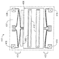
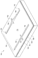
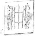
도 11은 다른 예시적인 셔터 어셈블리(1100)의 상면도를 도시한다. 셔터 어셈블리(1100)는, 셔터(1102), 2개의 정전식 액츄에이터들(1104), 및 기판(1108) 위에 셔터(1102) 및 액츄에이터들(1104)을 지지하는 앵커들(1106)을 포함한다. 셔터(903)와 유사하게, 셔터(1102)는, 함몰부들로 또한 지칭되는 립 톱니들의 세트를 포함한다. 더 상세하게, 셔터(1102)는 4개의 측면 함몰부들(1110) 및 2개의 장축 함몰부들(1112)을 포함한다.11 illustrates a top view of another
측면 함몰부들(1110)은, 셔터(1102)의 모션 방향과 수직한 길이를 갖는 셔터(1102)에 걸쳐 연장한다. 그들의 길이는, 셔터(1102)가 개방 포지션에 있는 경우 광이 관통하게 하기 위해 셔터(1102)에 형성된 셔터 어퍼쳐들(1114)의 세트와 평행하게 런한다. 셔터 어퍼쳐들(1114)은 셔터의 실질적으로 평면인 표면(1115)에 형성된다. 실질적으로 평면인 표면(1115)은, 대응하는 몰드의 최외각(outermost) 표면 상에 형성되었던 셔터의 일부에 대응한다.The
도 9의 셔터(902)의 립 톱니들(903)과는 대조적으로, 셔터(1102)의 측면 함몰부들(1110)은 셔터의 이웃한 에지들 사이의 거리의 실질적인 부분에 대해 연장한다. 몇몇 구현들에서, 측면 함몰부들(1110)은 셔터 에지들 사이의 거리의 적어도 약 50%, 예컨대, 셔터(1102)의 외주변 에지와 가장 가까운 셔터 어퍼쳐(1114)의 에지 사이의 거리 d1, 또는 이웃한 셔터 어퍼쳐들의 에지들 사이의 거리 d2를 고려한다. 몇몇 다른 구현들에서, 측면 함몰부들(1108)의 폭은 셔터 에지들 사이의 거리의 적어도 약 50%, 적어도 약 60%, 적어도 약 70%, 또는 적어도 약 80%를 고려한다. 측면 함몰부들(1110 및 1112)은 그들의 깊이 대 폭 애스팩트 비에 의해 추가적으로 특성화될 수 있다. 몇몇 구현들에서, 측면 함몰부들(1110 및 1112)의 깊이 대 폭은 적어도 약 1:1, 약 2:3 미만, 또는 약 1:2 미만이다. 추가적으로 후술되는 바와 같이, 비교적 넓은 함몰부들은, 폐쇄 포지션에 있는 경우 셔터의 하부측으로부터 반사하는 광이 셔터(1102)를 포함하는 디스플레이의 전면을 향해, 그리고 잠재적으로는 그로부터 바깥으로 역으로 반사하는 것을 방지하도록 기능한다.In contrast to the
장축 함몰부들(1112)은 셔터(1102)의 모션 방향과 평행한 길이를 갖는다. 그들은 셔터(1102)의 측면 에지들과 셔터 어퍼쳐들(1112)의 측면 에지들 사이에 로케이팅되며, 따라서, "측면 립들" 또는 "측면 함몰부들"로 지칭될 수도 있다. 측면 함몰부들(1110)과 유사하게, 장축 함몰부(1110)의 폭은, 셔터의 에지와 셔터 어퍼쳐들(1114)의 에지 사이의 거리의 실질적인 부분들을 고려한다. 몇몇 구현들에서, 장축 함몰부(1112)는 셔터(1102)의 실질적으로 전체 길이를 연장시킨다. 몇몇 다른 구현들에서, 장축 함몰부들(1112)은 더 짧다. 몇몇 다른 구현들에서, 셔터는 주어진 측면 상에, 교대로, 셔터(1102)의 길이를 따라 다수의 장축 함몰부들(1112)을 포함할 수도 있다.The
일반적으로, 장축 함몰부들(1112)은 셔터(1102)에 부가적인 강성을 제공하여, 셔터(1112)의 변형을 방지하는 것을 돕는다. 셔터 어퍼쳐들(905)을 관통하는 수직 벽들(909)에 의해 유사한 강성이 셔터 어셈블리(900)의 셔터(902)에 제공되었다. 그러나, 폐쇄 포지션에 있더라도 더 높은 각도의 광이 셔터(902)를 통해 누설되는 기회를 제공하기 위한, 이들 수직 벽들(909)의 기초부(base)에서의 개구들이 발견되었다. 장축 함몰부들(1112)의 형태로 어퍼쳐들의 외부의 수직 벽들을 이동시킴으로써, 셔터(1102)는 잠재적인 광 누설을 회피하면서 유사한 정도의 강성을 획득할 수 있다.In general, the
상술된 바와 같이, 개별적으로, 각각의 함몰부는 셔터 에지들 사이의 거리의 실질적인 부분을 고려한다. 집합적으로, 몇몇 구현들에서, 함몰부들은 또한, 셔터의 광 차단 부분들의 전체 영역의 실질적인 부분(즉, 셔터 어퍼쳐들(1112)을 배제하는 셔터(1102)의 영역)을 고려한다. 몇몇 구현들에서, 함몰부들은, 셔터(1102)의 광 차단 부분의 영역의 적어도 50%를 고려한다. 몇몇 다른 구현들에서, 함몰부들(1110 및 1112)은, 셔터(1102)의 광 차단 부분의 영역의 적어도 60%, 적어도 70%, 적어도 80% 또는 그 초과를 고려한다.As mentioned above, individually, each depression considers a substantial portion of the distance between the shutter edges. Collectively, in some implementations, the depressions also consider a substantial portion of the entire area of the light blocking portions of the shutter (i.e., the area of the
도 12는 다른 예시적인 셔터 어셈블리(1200)의 등척도를 도시한다. 셔터 어셈블리(1200)는 셔터(1202), 2개의 정전식 액츄에이터들(1204), 및 기판(1208) 위에 셔터(1202) 및 액츄에이터들(1204)을 지지하는 앵커들(1206)을 포함한다. 도 12에서, 도 11에 도시된 셔터(1102)와는 달리, 셔터(1202)는 3개의 어퍼쳐들(1212)을 둘러싸는 하나의 연속하는 함몰부(1207)를 포함한다. 별개의 측면 및 장축 함몰부들을 갖지는 않지만, 연속하는 함몰부(1207)는 측면 및 장축 함몰부 부분들을 갖는 것으로 고려될 수 있다. 도 11에 도시된 셔터(1102)의 별개의 측면 및 장축 함몰부들(1110 및 1112)과 유사하게, 연속하는 함몰부(1207)의 측면 및 장축 부분들 각각은 셔터의 이웃한 에지들 사이의 거리의 실질적인 부분을 고려한다. 다양한 구현들에서, 함몰부 부분들은, 이웃한 셔터 에지들 사이의 거리의 적어도 50%, 적어도 60%, 적어도 70%, 적어도 80% 또는 그 초과를 고려한다. 부가적으로, 몇몇 구현들에서, 연속하는 함몰부(1207)의 측면 부분들의 애스팩트 비는 약 1:1 미만, 약 2:3 미만, 또는 약 1:2 미만이다.FIG. 12 shows an isometric view of another
도 13은, 도 12의 셔터 어셈블리(1200)를 포함하는 예시적인 디스플레이 장치(1300)의 일부의 단면도를 도시한다. 디스플레이 장치(1300)는 MEMS-다운 구성에 따라 구축되며, 셔터 어셈블리(1200)는 폐쇄 포지션에 있다. 단면은 도 12의 라인 A-A'에 취해진다.Figure 13 shows a cross-sectional view of a portion of an
도 12 및 13을 참조하면, 디스플레이 장치(1300)는 어퍼쳐 플레이트(1350), 백라이트(1352), 및 광을 백라이트(1352)로 도입하기 위한 광 소스(1354)를 포함한다. 부가적으로, 블랙 매트릭스(도 12에 도시되지 않음)가 콘트라스트를 개선시키기 위해 기판(1210) 상에 증착된다. 어퍼쳐 플레이트(1350)는, 셔터 어셈블리(1200)에 의해 변조되기 위해 디스플레이의 전면을 향해 광이 백라이트(1352)를 탈출할 수 있는 어퍼쳐들(1358)을 정의하는 어퍼쳐 층(1356)을 포함한다. 몇몇 구현들에서, 어퍼쳐 층(1356)은, 반사성 층을 대면하는 후면 및 광 흡수층을 대면하는 전면을 포함한다.12 and 13, the
디스플레이 장치(1300)에서, 셔터 어셈블리(1200)의 연속하는 함몰부(1207)는 기판(1210)을 향해 돌출하며, 기판 상에서 그 함몰부는, 연속하는 함몰부(1207)가 어퍼쳐 층(1356)을 향해 개방되도록 구축되었다. 이러한 구성에서, 셔터(1202)가 폐쇄 포지션에 있는 경우, 최대 각도(at most angle)들로 어퍼쳐 층(1356)을 통해 탈출하는 광은, 연속하는 함몰부(1207)의 내부 표면 상에서 셔터(1202)에 충돌한다. 따라서, 이러한 광이 디스플레이 장치(1300)의 전면을 향해 역으로 반사될 수 있기 전에, 함몰부(1207)의 2개가 아닌 적어도 하나의 부가적인 내부 표면들로부터 반사할 가능성이 있다. 셔터(1202)가 매우 반사성있는 재료로부터 제조되지 않으므로, 각각의 반사는 나머지 광 에너지의 실질적인 부분을 흡수하며, 그에 의해, 디스플레이 장치(1300)로부터 잠재적으로 누설될 수도 있는 광의 양을 상당히 감소시킨다.The
도 13에 도시된 바와 같이, 연속하는 함몰부(1207)의 폭(Wd)은 어퍼쳐들의 폭(Wa)에 비해 상당히 크다. 도시된 바와 같이, Wd는 Wa보다 크다. 몇몇 다른 구현들에서, Wd는 Wa의 사이즈의 적어도 50%이다. 몇몇 다른 구현들에서, Wd는 Wa의 적어도 60%, 적어도 70%, 또는 적어도 80%이다. Wa에 비해 Wd의 비교적 큰 사이즈는, 함몰부(1307)의 내부 표면에 콘택트할 시에 광이 어퍼쳐들을 관통하게 촉진하는 것을 돕는다.As shown in Fig. 13, the width W d of the
도 14는 다른 예시적인 디스플레이 장치(1400)의 일부의 단면도를 도시한다. 디스플레이 장치(1400)는 도 1400의 디스플레이 장치(1400)와 실질적으로 유사하지만, 디스플레이 장치(1400)는 MEMS-업 구성으로 구축된다. 즉, 디스플레이 장치(1400)에 포함된 셔터 어셈블리, 즉 셔터 어셈블리(1402)는 도 14에 도시된 바와 같이, 반대의 기판 대신 어퍼쳐 플레이트(1404) 상에 직접 형성된다. 셔터 어셈블리(1300)와 유사한 셔터 어셈블리(1402)는, 수 개의 셔터 어퍼쳐들(1408)을 둘러싸는 측면 함몰부 부분들 및 장축 함몰부 부분들을 갖는 연속하는 함몰부를 갖는 셔터(1406)를 포함한다. 측면 함몰부 부분들(1410)만이 도 14에 도시된 단면에서 가시적이다.FIG. 14 shows a cross-sectional view of a portion of another
도 11-14에서, 셔터 어셈블리들 각각에 포함된 함몰부들은, 표면들이 구축되었던 기판의 표면에 평행하거나 수직하지 않았던 그 표면들을 갖는 실질적으로 수직인 측벽들을 포함했다. 다른 함몰부 형상들이 몇몇 다른 구현들에서 이용될 수도 있다. 부가적으로, 도시된 셔터 어셈블리들 각각은 임의의 쌍의 이웃한 셔터 에지들 사이에 단일 함몰부(또는 함몰부 부분)만을 포함했다. 몇몇 다른 구현들에서, 셔터들은 이웃한 셔터 에지들 사이에 다수의 함몰부들을 포함할 수 있다. 몇몇 다른 구현들에서, 함몰부들은 셔터 에지들 사이의 거리 중 작은 것을 고려하며, 그 후, 상기와 같이 제안되었다.In Figures 11-14, the depressions included in each of the shutter assemblies included substantially vertical sidewalls having surfaces that were not parallel or perpendicular to the surface of the substrate upon which the surfaces were built. Other depression shapes may be used in some other implementations. Additionally, each of the illustrated shutter assemblies included only a single depression (or depression portion) between any pair of adjacent shutter edges. In some other implementations, the shutters may include a plurality of depressions between adjacent shutter edges. In some other implementations, the depressions take into account the small of the distance between the shutter edges, and thereafter proposed as above.
도 15a-15i는 셔터 함몰부들에 적절한 예시적인 대안적인 단면 형상들을 도시한다. 도 15a-15i에 도시된 단면 형상들 각각은 도 11에 도시된 단면 B-B'에 대한 형상들에 대응한다.Figures 15A-15I illustrate exemplary alternative cross-sectional shapes suitable for shutter depressions. Each of the cross-sectional shapes shown in Figs. 15A-15I corresponds to the shapes for the cross-section B-B 'shown in Fig.
도 15a는 경사진 벽들을 갖는 셔터 함몰부(1500)의 단면을 도시한다. 도 15b는 오목한 경사진 벽들을 갖는 셔터 함몰부(1510)의 단면을 도시한다. 도 15c는 실질적으로 원형인 함몰부(1520)를 포함한다.15A shows a cross section of a
도 15d 및 도 15e는 V-형상 함몰부들(1530)을 도시한다. 도 15c에 도시된 V-형상 함몰부(1530)가 셔터 에지들 사이의 거리의 실질적인 부분을 취하지 않지만, 몇몇 다른 구현들에서, 훨씬 더 얕은 각도들을 갖는 V-형상 함몰부들이 형성될 수 있다. 그러한 얕은 V-형상 함몰부들은 그러한 거리의 실질적인 부분을 고려할 수 있다. 대안적으로, 도 15e에 도시된 바와 같이, 셔터는, 2개의 이웃한 셔터 에지들 사이에 다수의 V-형상 함몰부들(1530)을 포함할 수 있다. 도 15e에서, 3개의 V-형상 함몰부들(1530)은 함께, 셔터 에지들 사이의 거리의 실질적인 부분을 고려한다.Figs. 15d and 15e illustrate V-shaped
도 15f-15i는, 실질적으로 수평이고 실질적으로 수직인 표면들을 보유하면서 직사각형 함몰부들(1540)을 산출하는 대안적인 셔터 단면 형상들을 도시한다. 도 15f는, 다수의 비교적 낮은-애스팩트 비 직사각형 함몰부들(1540)을 포함하는 셔터의 일부를 도시한다. 도 15g는, 셔터 부분의 중심으로부터 오프셋된 직사각형 함몰부(1540)를 갖는 셔터의 일부를 도시한다. 즉, 직사각형 함몰부(1540)는 셔터 에지들 중 하나에 다른 것보다 더 근접하다. 도 15h는, 셔터 부분의 어느 하나의 에지에 수직 측면 벽들을 갖는 중앙의 직사각형 함몰부(1540)를 갖춘 셔터 부분을 도시한다. 도 15i는 셔터 부분의 어느 하나의 단부에서 2개의 직사각형 함몰부들(1540)을 갖는 셔터 부분을 도시한다. 실질적으로 평면인 표면은 직사각형 함몰부들(1540)을 분리시킨다.15F-15i illustrate alternative shutter cross-sectional shapes that produce
도 15a-15i에 도시된 대안적인 셔터 단면 형상들 각각은, 도 7a-7d에 관련하여 상술된 것들과 유사한 제조 프로세스들을 사용하여 달성될 수 있다. 상세하게, 몇몇 구현들에서, 도시된 셔터 부분들을 포함하는 셔터들은, 2개의 계층화된 몰드 상으로 증착된 구조 재료들을 패터닝 및 에칭함으로써 형성된다. 몰드의 최상단 표면 상에 증착된 재료는, MEMS-다운 배향으로(즉, 도 15a-15i에 도시된 배향으로) 배치되는 경우 셔터 부분들의 하부 표면으로서 기능한다. 각각의 함몰부들의 하단은 2개의 몰드 층들 사이의 계면에 증착된 재료로부터 형성된다. 몰드에 형성된 형상들은 표준 포토패터닝 및 에칭 프로세스들을 사용하여 형성될 수 있다. 예를 들어, 경사진-벽 함몰부(1500) 또는 V-형상 함몰부들(1530)의 각진 표면들은, 몰드 재료로의 노출 광의 침투를 변경시키기 위해 하프톤(halftone) 또는 고에너지 빔-민감형 유리 마스크들을 사용하여 상부 몰드 층을 패터닝함으로써 달성될 수 있다. 오목한-벽 셔터 함몰부(1510)와 같은 다른 형상들은, 리프트-오프(lift-off) 프로세스들에서 일반적으로 사용되는 오목-각 몰드 재료를 사용함으로써 달성될 수 있다.Each of the alternative shutter cross-sectional shapes shown in Figures 15A-15i may be accomplished using manufacturing processes similar to those described above with respect to Figures 7A-7D. Specifically, in some implementations, the shutters, including the illustrated shutter portions, are formed by patterning and etching structured materials deposited on two layered molds. The material deposited on the top surface of the mold functions as the bottom surface of the shutter portions when disposed in the MEMS-down orientation (i.e., in the orientation shown in Figures 15A-15i). The bottom of each depression is formed from the material deposited at the interface between the two mold layers. The shapes formed in the mold can be formed using standard photo patterning and etching processes. For example, the angled surfaces of the tilted-
15h에 도시된 셔터 부분은, 셔터 부분의 에지들이 백라이트를 탈출하는 광의 다이렉트(direct) 경로로부터의 것이라는 점에서 부가적인 이점들을 제공한다. 상술된 바와 같이, 몇몇 구현들에서, 본 명세서에 설명된 셔터들은 내부 금속층을 포함하는 재료의 수 개의 층들로부터 형성된다. 그러한 셔터들의 에지들이 상부 또는 하부 몰드 층들에 실질적으로 평행하면, 셔터들을 제조할 시에 사용되는 이방성 에칭 프로세스 및/또는 릴리즈 프로세스는, 그들 에지들에서 외부 셔터 층의 일부들을 제거하여, 하부 내부 금속층을 노출시킬 수 있다.The shutter portion shown at 15h provides additional advantages in that the edges of the shutter portion are from a direct path of light escaping the backlight. As noted above, in some implementations, the shutters described herein are formed from several layers of material including an inner metal layer. If the edges of such shutters are substantially parallel to the upper or lower mold layers, the anisotropic etch process and / or the release process used in making the shutters may remove portions of the outer shutter layer at their edges, .
노출된 셔터 에지들은 디스플레이 장치의 전면을 향해 높은 입사각 광을 굴절시킬 수 있다. 이러한 굴절 현상이 도 14에 도시된다. 도 14에서, 광(1450)은 디스플레이 장치(1400)의 전면을 향해 셔터(1402)의 최우측 부분의 에지로부터 굴절된다. 그러한 광이 디스플레이를 탈출하는 것을 방지하고, 그에 의해 그의 콘트라스트 비를 감소시키기 위해, 디스플레이 장치(1400)의 블랙 매트릭스(1460)는 중첩부 O에 의해 셔터(1402)의 에지를 실질적으로 중첩하도록 적용된다. 이러한 중첩이 굴절 현상으로부터 초래하는 광 누설을 방지하지만, 그것은, 디스플레이로부터 방출될 수 있는 각도들의 범위 및 애스팩트 비를 감소시킨다. 도 15h에 도시된 바와 같이, 높은 각도 광의 경로 바깥에 셔터 에지들을 로케이팅시키는 것은, 셔터 에지로부터의 굴절로부터의 광 누설에 대한 잠재성을 감소시킬 수 있고, 몇몇 경우들에서는 제거할 수 있으며, 그에 의해, 블랙 매트릭스 중첩을 위한 이유를 제거한다. 따라서, 그러한 셔터들을 포함하는 디스플레이들은 블랙 매트릭스에서 개구들을 연장시킬 수 있으며, 증가된 시야각들 및 더 밝은 디스플레이들을 제공한다.The exposed shutter edges may refract high incident angle light toward the front of the display device. This refraction phenomenon is shown in Fig. In Fig. 14, light 1450 is refracted from the edge of the rightmost portion of
도 16a는, 각진 주변 표면들을 갖는 예시적인 셔터(1600)의 상면도를 도시한다. 도 16b는 도 16a의 셔터(1600)의 단면도를 도시한다. 단면은 도 16a의 라인 C-C'에서 취해진다. 도 16a 및 16b를 참조하면, 셔터(1600)는 2개의 셔터 어퍼쳐들(1604)을 둘러싸는 연속하는 함몰부(1602)를 포함한다. 셔터(1600)는 2개의 타입들의 각진 주변 표면들, 즉 각진 외부 주변 표면(1606), 및 각각의 셔터 어퍼쳐(1604) 주변에 하나씩 있는 2개의 각진 셔터 어퍼쳐 주변 표면들(1608)(집합적으로, "각진 주변 표면들(1606 및 1608)")을 포함한다. 각진 주변 표면들(1606 및 1608)은, 연속하는 함몰부(1602)와 동일한 방향으로 셔터의 최상단 표면들(1610)로부터 떨어져 아래로 각져있다. 도 16a 및 16b 둘 모두에서, 셔터(1600)는 셔터가 몰드에서 어떻게 형성될지의 관점으로부터 도시된다. 따라서, 몇몇 구현들에서, 디스플레이 장치로 도입된 경우, 셔터(1600)는, 연속하는 함몰부(1602)가 디스플레이 장치의 후면을 향해 개방될 것이고 각진 주변 표면들(1606 및 1608)이 디스플레이 장치의 전면을 향해 연장되도록 플립될 것이다.16A shows a top view of an
몇몇 구현들에서, 각진 주변 표면들(1606 및 1608)은, 셔터(1600)의 평면의 약 20도와 약 70도 사이에서 각져있다. 몇몇 구현들에서, 각진 주변 표면들(1606 및 1608)은 셔터의 평면의 약 40도와 약 50도 사이에서 각져있다. 몇몇 다른 구현들에서, 각진 주변 표면들(1606 및 1608)은 셔터의 평면의 45도로 각져있다. 일반적으로, 선택된 각도는, 연속하는 함몰부(1602)의 폭, 셔터(1600)가 폐쇄 포지션에 있는 경우, 각진 주변 표면들(1606 및 1608)이 어퍼쳐 층의 대응하는 부분들과 중첩하는 정도, 및 수반한 블랙 매트릭스의 치수들 중 하나 또는 그 초과의 함수이다. 몇몇 구현들에서, 외주변 표면(1606)은 셔터 어퍼쳐 주변 표면들(1608)과 동일한 각도로 각져있다. 몇몇 구현들에서, 외주변 표면(1606)은 셔터 어퍼쳐 주변 표면들(1608)과는 상이한 각도로 각져있다. 셔터(1600)의 또 다른 몇몇 구현들에서, 외주변 표면(1606)만이 또는 셔터 어퍼쳐 주변 표면들(1608)만이 각져있다.In some implementations, the angled
이러한 구현에서, 연속하는 함몰부(1602)의 벽들은, 셔터(1600)의 평면에 실질적으로 수직하거나 직교한다. 몇몇 구현들에서, 연속하는 함몰부(1602)의 벽들이 또한 각져있다.In this implementation, the walls of the
도 17은 각져있는 주변 표면들을 갖는 예시적인 셔터를 형성하기 위한 몰드(1700)의 예시적인 단면을 도시한다. 예를 들어, 몰드(1700)는 도 16a 및 16b의 셔터(1600)를 형성하기 위해 사용될 수 있다. 도 16a, 16b 및 17을 참조하면, 예를 들어, 2개의 레벨들로 수평 표면들을 포함하는 도 7a-7c 또는 도 10에 관련하여 상술된 몰드들과는 달리, 몰드(1700)는 3개의 레벨들로 수평 표면들을 포함한다. 그러나, 몰드(1700)는, 단지 2개의 층들의 몰드 재료로부터 여전히 제조되며, 따라서, 여전히 2개의 패터닝 단계들만을 사용하여 완전히 패터닝될 수 있다. 낮은-레벨 수평 표면들(1702)은 하부 몰드 재료(1704)와 상부 몰드 재료(1706) 사이의 계면(1703)에 대응한다. 이들 낮은-레벨 수평 표면들(1702) 상에서, 셔터(1600)의 연속하는 함몰부(1602)의 플로어가 형성된다. 중간-레벨 수평 표면들(1708)은, 셔터 어퍼쳐들(1604) 및 셔터들 사이의 공간들을 형성하기 위해 에칭될 영역들에 대응한다. 최상단 수평 표면들(1710)은, 셔터(1600)의 최상단 표면들(1610)이 형성되는 영역들에 대응한다.Figure 17 shows an exemplary cross-section of a
도 18은 각진 주변 표면들을 갖는 셔터(1802)를 포함하는 예시적인 디스플레이 장치(1800)의 일부의 단면을 도시한다. 디스플레이 장치(1800)는, 폐쇄 포지션에 있는 셔터(1802)를 이용하여 MEMS-up 구성에 따라 구축된다.18 shows a cross section of a portion of an
셔터(1802)는 어퍼쳐 플레이트(1850) 상에 형성된 셔터 어셈블리(1803)의 일부이다. 디스플레이 장치(1800)는 또한, 백라이트(1852) 및 백라이트(1852)로 광을 도입하기 위한 광 소스(1854)를 포함한다. 부가적으로, 블랙 매트릭스(1855)는 콘트라스트를 개선시키기 위해 커버 플레이트(1810) 상에 증착된다. 어퍼쳐 플레이트(1850)는, The
셔터 어셈블리(1803)에 의해 변조되기 위해 디스플레이 장치(1800)의 전면을 향해 광이 백라이트(1852)를 탈출할 수 있는 어퍼쳐들(1858)을 정의하는 어퍼쳐 층(1856)을 포함한다. 몇몇 구현들에서, 어퍼쳐 층(1856)은 반사성 층을 대면하는 후면 및 광 흡수층을 대면하는 전면을 포함한다.And an
디스플레이 장치(1800)에서, 셔터(1802)는, 함몰부(1807)가 어퍼쳐 층(1856)을 향해 개방되도록 커버 플레이트(1810)를 향해 돌출하는 연속하는 함몰부(1807)를 포함한다. 이러한 구성에서, 셔터(1806)가 폐쇄되는 경우, 최대 각도들로 어퍼쳐 층(1856)을 통해 탈출하는 광은 연속하는 함몰부(1807)의 내부 표면 상에서 셔터(1802)에 충돌한다. 따라서, 이러한 광이 디스플레이 장치(1800)의 전면을 향해 역으로 반사될 수 있기 전에, 연속하는 함몰부(1807)의 2개가 아닌 적어도 하나의 부가적인 내부 표면들로부터 반사할 가능성이 있다.In the
도 18에 도시된 바와 같이, 연속하는 함몰부의 폭(Wd)은 어퍼쳐들의 폭(Wa)에 비해 상당히 크다. 도시된 구현에서, Wd가 Wa보다 작지만, Wd는 Wa의 사이즈의 여전히 적어도 80%이다. 몇몇 다른 구현들에서, Wd는 Wa의 사이즈의 적어도 50%이다. 몇몇 다른 구현들에서, Wd는 Wa의 적어도 60% 또는 적어도 70%이다. 또 다른 구현들에서, Wd는 Wa보다 크다. Wa에 비해 Wd의 비교적 큰 사이즈는, 함몰부(1807)의 내부 표면에 콘택트할 시에 광이 어퍼쳐들을 관통하게 촉진하는 것을 돕는다.As shown in Fig. 18, the width W d of successive depressions is considerably larger than the width W a of the upper actuators. In the illustrated implementation, W d is less than W a , but W d is still at least 80% of the size of W a . In some other implementations, W d is at least 50% of the size of W a . In some other implementations, W d is at least 60% or at least 70% of W a . In yet other implementations, W d is greater than W a . The relatively large size of W d relative to W a helps to facilitate light through the apertures when contacting the inner surface of
도 14의 디스플레이 장치(1400)와는 대조적으로, 디스플레이 장치(1800)의 셔터 어셈블리(1803)는, 각진 주변 표면들(1812)을 갖는 셔터(1802)를 포함한다. 따라서, 셔터(1802)의 에지들은, 도 14의 디스플레이 장치에서 셔터(1307)의 에지들로부터 굴절되었던 높은 각도의 광의 경로 외부에 있다. 결과로서, 디스플레이 장치(1800)는, 블랙 매트릭스(1855)와 셔터(1802)의 에지들 사이의 중첩을 포기한다. 대신, 몇몇 구현들에서, 블랙 매트릭스(1855)의 에지들은 셔터(1802)의 에지들과 실질적으로 정렬한다.In contrast to the
도 19는 각진 주변 표면들을 갖는 셔터(1902)를 포함하는 다른 예시적인 디스플레이 장치(1900)의 일부의 단면을 도시한다. 디스플레이 장치(1900)는, 폐쇄 포지션에 있는 셔터(1902)를 이용하여 MEMS-up 구성에 따라 구축된다. 도 18의 디스플레이 장치(1800)의 셔터(1802)와는 대조적으로, 셔터(1902)는 2개의 연속하는 함몰부들(1904)을 포함한다. 부가적으로, 각각의 함몰부(1904)의 하나의 벽은, 함몰부들이 셔터(1902)의 에지들 바로 위로 연장하므로 각진 주변 표면으로서 기능한다. 또한, 셔터(1902)의 각진 표면들은 전면 대신 디스플레이 장치(1900)의 후면을 향해 연장한다. 셔터의 에지들까지 포지셔닝되는 함몰부들은 광을 트랩핑(trap)할 시에 특히 효율적이다. 또한, 각진 주변 표면들을 형성하기 위해 셔터(1902)의 에지들을 각지게 함으로써, 광이 디스플레이 장치(1900)의 전면을 향해 굴절할 가능성이 작아진다.19 illustrates a cross section of a portion of another
도 20은, 각진 주변 표면들을 갖는 셔터(2002)를 포함하는 다른 예시적인 디스플레이 장치(2000)의 일부의 단면을 도시한다. 디스플레이 장치(2000)는, 폐쇄 포지션에 있는 셔터(2002)를 이용하여 MEMS-up 구성에 따라 구축된다. 도 19의 디스플레이 장치(1900)의 셔터(1902)와는 대조적으로, 셔터(2002)는, 셔터의 외부 벽을 형성하고 셔터 어퍼쳐를 둘러싸는 각진 주변 표면들(2006)에 의해 경계지어진 단일의 큰 연속하는 함몰부(2004)만을 포함한다. 도 19의 셔터(1902)와 유사하게, 셔터(2002)의 각진 표면들(2006)은 전면 대신 디스플레이 장치(2000)의 후면을 향해 연장한다. 셔터의 에지들까지 연장하는 함몰부(2004)는 광을 트랩핑할 시에 특히 효율적이다. 또한, 각진 주변 표면들(2006)을 형성하기 위해 셔터(2002)의 에지들을 각지게 함으로써, 광이 디스플레이 장치(2000)의 전면을 향해 굴절할 가능성이 작아진다.20 illustrates a cross-section of a portion of another
본 명세서에 기재된 구현들과 관련하여 설명된 다양한 예시적인 로직들, 로직 블록들, 모듈들, 회로들 및 알고리즘 프로세스들은 전자 하드웨어, 컴퓨터 소프트웨어, 또는 이 둘의 결합들로서 구현될 수도 있다. 하드웨어와 소프트웨어의 상호교환가능성은, 기능의 관점들에서 일반적으로 설명되었고, 상술된 다양한 예시적인 컴포넌트들, 블록들, 모듈들, 회로들, 및 프로세스들에서 도시되었다. 그러한 기능이 하드웨어로 구현되는지 또는 소프트웨어로 구현되는지는 특정한 애플리케이션 및 전체 시스템에 부과된 설계 제약들에 의존한다.The various illustrative logics, logic blocks, modules, circuits, and algorithm processes described in connection with the implementations described herein may be implemented as electronic hardware, computer software, or combinations of both. The interchangeability of hardware and software has been generally described in terms of functionality and is illustrated in the various exemplary components, blocks, modules, circuits, and processes described above. Whether such functionality is implemented in hardware or software depends upon the particular application and design constraints imposed on the overall system.
본 명세서에 기재된 양상들과 관련하여 설명된 다양한 예시적인 로직들, 로직 블록들, 모듈들 및 회로들을 구현하는데 사용되는 하드웨어 및 데이터 프로세싱 장치는, 범용 단일- 또는 멀티-칩 프로세서, 디지털 신호 프로세서(DSP), 주문형 집적회로(ASIC), 필드 프로그래밍가능 게이트 어레이(FPGA) 또는 다른 프로그래밍가능 로직 디바이스, 이산 게이트 또는 트랜지스터 로직, 이산 하드웨어 컴포넌트들, 또는 본 명세서에 설명된 기능들을 수행하도록 설계된 이들의 임의의 결합으로 구현 또는 수행될 수도 있다. 범용 프로세서는 마이크로프로세서, 또는 임의의 종래의 프로세서, 제어기, 마이크로제어기, 또는 상태 머신일 수도 있다. 프로세서는 또한 컴퓨팅 디바이스들의 결합, 예를 들어, DSP와 마이크로프로세서의 결합, 복수의 마이크로프로세서들, DSP 코어와 결합한 하나 또는 그 초과의 마이크로프로세서들, 또는 임의의 다른 그러한 구성으로서 구현될 수도 있다. 몇몇 구현들에서, 특정한 프로세스들 및 방법들은, 주어진 기능에 특정한 회로에 의해 수행될 수도 있다.The hardware and data processing apparatus used to implement the various illustrative logic, logic blocks, modules, and circuits described in connection with the aspects disclosed herein may be implemented or performed with a general purpose single- or multi-chip processor, a digital signal processor (DSP), an application specific integrated circuit (ASIC), a field programmable gate array (FPGA) or other programmable logic device, discrete gate or transistor logic, discrete hardware components, or any of those designed to perform the functions described herein May be implemented or performed in combination. A general purpose processor may be a microprocessor, or any conventional processor, controller, microcontroller, or state machine. The processor may also be implemented as a combination of computing devices, e.g., a combination of a DSP and a microprocessor, a plurality of microprocessors, one or more microprocessors in conjunction with a DSP core, or any other such configuration. In some implementations, the specific processes and methods may be performed by circuitry specific to a given function.
하나 또는 그 초과의 양상들에서, 설명된 기능들은 본 명세서에 기재된 구조들 및 그 구조들의 그들의 구조적 등가물들을 포함하는, 하드웨어, 디지털 전자 회로, 컴퓨터 소프트웨어, 펌웨어, 또는 이들의 임의의 결합으로 구현될 수도 있다. 본 명세서에 설명된 요지의 구현들은 또한, 하나 또는 그 초과의 컴퓨터 프로그램들, 즉 데이터 프로세싱 장치에 의한 실행을 위해 또는 데이터 프로세싱 장치의 동작을 제어하기 위해 컴퓨터 저장 매체들 상에 저장된 컴퓨터 프로그램 명령들의 하나 또는 그 초과의 모듈들로서 구현될 수 있다.In one or more aspects, the functions described may be implemented in hardware, digital electronic circuitry, computer software, firmware, or any combination thereof, including the structures described herein and their structural equivalents thereof It is possible. Implementations of the subject matter described herein may also be embodied in the form of computer program instructions stored on computer storage media for execution by one or more computer programs, a data processing apparatus, or for controlling the operation of a data processing apparatus May be implemented as one or more modules.
본 발명에 설명된 구현들에 대한 다양한 변형들은 당업자들에게는 용이하게 명백할 것이며, 본 명세서에 정의된 일반적인 원리들은 본 발명의 사상 또는 범위를 벗어나지 않으면서 다른 구현들에 적용될 수도 있다. 따라서, 청구항들은 본 명세서에 설명된 구현들로 제한되도록 의도되는 것이 아니라, 본 명세서에 기재된 본 발명, 원리들 및 신규한 특성들에 일치하는 가장 넓은 범위를 부여할 것이다.Various modifications to the implementations described herein will be readily apparent to those skilled in the art, and the generic principles defined herein may be applied to other implementations without departing from the spirit or scope of the invention. Accordingly, the claims are not intended to be limited to the embodiments described herein, but are to be accorded the widest scope consistent with the invention, principles and novel features set forth herein.
부가적으로, 당업자는, 용어들 "상부" 및 "하부"가 종종 도면들을 설명하려는 용이함을 위해 사용되고, 적절히 지향된 페이지 상의 도면의 지향에 대응하는 상대적인 포지션들을 표시하며, 구현된 바와 같은 임의의 디바이스의 적절한 배향을 반영하지는 않을 수도 있음을 용이하게 인식할 것이다.Additionally, those skilled in the art will recognize that the terms "upper" and "lower" are often used for ease of describing the drawings, indicate relative positions corresponding to the orientation of the drawing on a properly oriented page, But may not reflect the proper orientation of the device.
별개의 구현들의 맥락에서 본 명세서에 설명된 특정한 특성들은 또한, 단일 구현의 결합으로 구현될 수 있다. 대조적으로, 단일 구현의 맥락에서 설명된 다양한 특성들은 또한, 다수의 구현들에서 별개로 또는 임의의 적절한 서브결합으로 구현될 수 있다. 또한, 특성들이 특정한 결합들에서 작동하는 바와 같이 상술되고, 그러므로 심지어는 초기에 청구될 수도 있지만, 몇몇 경우들에서, 청구된 결합으로부터의 하나 또는 그 초과의 특성들은 결합으로부터 삭제될 수 있으며, 청구된 결합은 서브결합 또는 서브결합의 변경에 관련될 수도 있다.Certain features described herein in the context of separate implementations may also be implemented in conjunction with a single implementation. In contrast, the various features described in the context of a single implementation may also be implemented separately or in any suitable sub-combination in multiple implementations. In addition, in some cases, one or more of the characteristics from the claimed combination may be removed from the combination, as the features are described above as operating in certain combinations and may even be claimed initially, A combination may be associated with a sub-combination or a modification of a sub-combination.
유사하게, 동작들이 특정한 순서로 도면들에 도시되었지만, 이것은, 바람직한 결과들을 달성하기 위해, 그러한 동작들이 도시된 특정한 순서 또는 순차적인 순서로 수행되거나, 모든 도시된 동작들이 수행된다는 것을 요구하는 것으로 이해되지는 않아야 한다. 추가적으로, 도면들은, 흐름도의 형태로 하나 또는 그 초과의 예시적인 프로세스들을 도식적으로 도시할 수도 있다. 그러나, 도시되지 않은 다른 동작들이 도식적으로 도시된 예시적인 프로세스들에 포함될 수 있다. 예를 들어, 하나 또는 그 초과의 부가적인 동작들이 임의의 도시된 동작들 이전에, 이후에, 동시에 또는 그들 사이에서 수행될 수 있다. 특정한 환경들에서, 멀티태스킹 및 병렬 프로세싱이 유리할 수도 있다. 또한, 상술된 구현들에서의 다양한 시스템 컴포넌트들의 분리는, 모든 구현들에서 그러한 분리를 요구하는 것으로 이해되지 않아야 하며, 설명된 프로그램 컴포넌트들 및 시스템들이 일반적으로 단일 소프트웨어 물건으로 함께 통합되거나 다수의 소프트웨어 물건들로 패키징될 수 있음을 이해해야 한다. 부가적으로, 다른 구현들은 다음의 청구항들의 범위 내에 있다. 몇몇 경우들에서, 청구항들에서 인용된 동작들은 상이한 순서로 수행될 수 있으며, 여전히 바람직한 결과들을 달성할 수 있다.Similarly, although operations are shown in the figures in a particular order, it is understood that such operations are performed in the specific order or sequential order shown, or that all illustrated operations are performed, in order to achieve the desired results It should not be. Additionally, the drawings may schematically illustrate one or more exemplary processes in the form of a flowchart. However, other operations not shown may be included in the exemplary processes illustrated schematically. For example, one or more additional operations may be performed before, after, simultaneously with, or between any of the depicted operations. In certain circumstances, multitasking and parallel processing may be advantageous. Also, the separation of the various system components in the above-described implementations should not be understood as requiring such separation in all implementations, and the described program components and systems may generally be integrated together into a single software article, It should be understood that they can be packaged as objects. Additionally, other implementations are within the scope of the following claims. In some instances, the operations recited in the claims may be performed in a different order and still achieve desirable results.
Claims (35)
백라이트;
상기 백라이트의 전면에 포지셔닝되고 복수의 어퍼쳐들을 정의하는 어퍼쳐 층; 및
상기 디스플레이 장치 상에 이미지를 형성하기 위해 상기 어퍼쳐들을 관통하는 상기 백라이트에 의해 방출된 광을 변조하도록 구성된 마이크로전자기계 시스템(MEMS) 광 변조기를 포함하며,
상기 MEMS 광 변조기는 셔터를 포함하고,
상기 셔터는,
어퍼쳐 층-대면 표면 및 전면-대면 표면을 갖는 광 차단 부분; 및
상기 광 차단 부분에 형성된 적어도 하나의 함몰부(depression) - 상기 적어도 하나의 함몰부의 폭은, 상기 셔터의 2개의 에지들을 분리시키는 거리의 적어도 50%이지만 100% 미만을 고려함 - 를 갖는, 디스플레이 장치.As a display device,
Backlight;
An aperture layer positioned on a front surface of the backlight and defining a plurality of apertures; And
And a micro electro mechanical system (MEMS) optical modulator configured to modulate light emitted by the backlight through the apertures to form an image on the display device,
Wherein the MEMS optical modulator comprises a shutter,
The shutter
A light blocking portion having an aperture layer-facing surface and a front-facing surface; And
At least one depression formed in the light intercepting portion, the width of the at least one depression being at least 50% but less than 100% of the distance separating the two edges of the shutter, .
상기 적어도 하나의 함몰부는 상기 어퍼쳐 층을 향해 개방되는, 디스플레이 장치.The method according to claim 1,
Wherein the at least one depression is open toward the aperture layer.
상기 적어도 하나의 함몰부는, 폭이 깊이보다 크도록 길이, 상기 폭, 및 상기 깊이를 갖는, 디스플레이 장치.The method according to claim 1,
Wherein the at least one depression has a length, width, and depth such that the width is greater than the depth.
상기 셔터는, 개방 포지션에서 광이 상기 셔터를 관통하게 하기 위한 셔터 어퍼쳐를 더 포함하고,
상기 셔터의 2개의 에지들은 상기 셔터의 외주변(outer perimeter) 에지 및 상기 셔터 어퍼쳐의 에지를 포함하는, 디스플레이 장치.The method according to claim 1,
Wherein the shutter further comprises a shutter aperture for causing light to pass through the shutter at an open position,
Wherein the two edges of the shutter comprise an outer perimeter edge of the shutter and an edge of the shutter aperture.
상기 셔터는, 상기 셔터의 에지의 외주변과 상기 셔터 어퍼쳐의 에지 사이에 적어도 2개의 함몰부들을 포함하는, 디스플레이 장치.5. The method of claim 4,
Wherein the shutter includes at least two depressions between an outer periphery of an edge of the shutter and an edge of the shutter aperture.
상기 셔터는,
개방 포지션에서, 광이 상기 셔터를 관통하게 하기 위한 셔터 어퍼쳐; 및
측면 함몰부의 길이가 상기 셔터 어퍼쳐의 길이와 수직하도록 상기 셔터 어퍼쳐와 상기 셔터의 측면 사이에 포지셔닝된 상기 측면 함몰부를 더 포함하는, 디스플레이 장치.The method according to claim 1,
The shutter
A shutter aperture in the open position for allowing light to pass through the shutter; And
The side depression being positioned between the shutter aperture and the side surface of the shutter so that the length of the side depression is perpendicular to the length of the shutter aperture.
상기 적어도 하나의 함몰부는, 적어도 하나의 장축(longitudinal) 함몰부 부분 및 적어도 하나의 측면 함몰부 부분을 포함하는, 디스플레이 장치.The method according to claim 1,
Wherein the at least one depression comprises at least one longitudinal depression portion and at least one side depression portion.
상기 셔터는, 적어도 약 20도인, 디스플레이의 법선에 대한 각도를 갖는 주변 표면을 포함하는, 디스플레이 장치.The method according to claim 1,
Wherein the shutter comprises a peripheral surface having an angle to the normal of the display that is at least about 20 degrees.
상기 디스플레이 법선에 대한 상기 주변 표면의 각도는 약 70도 미만인, 디스플레이 장치.9. The method of claim 8,
Wherein an angle of the peripheral surface with respect to the display normal is less than about 70 degrees.
상기 광 차단 부분에 형성된 적어도 하나의 함몰부는, 상기 어퍼쳐 층 내의 대응하는 어퍼쳐보다 더 넓은, 디스플레이 장치.The method according to claim 1,
Wherein at least one depression formed in the light shielding portion is wider than a corresponding aperture in the aperture layer.
백라이트;
상기 백라이트의 전면에 포지셔닝되고 복수의 어퍼쳐들을 정의하는 어퍼쳐 층; 및
상기 디스플레이 장치 상에 이미지를 형성하기 위해 상기 어퍼쳐들을 관통하는 상기 백라이트에 의해 방출된 광을 변조하도록 구성된 마이크로전자기계 시스템(MEMS) 광 변조기를 포함하며,
상기 MEMS 광 변조기는 셔터를 포함하고,
상기 셔터는,
어퍼쳐 층-대면 표면 및 전면-대면 표면을 갖는 광 차단 부분;
광이 개방 포지션에 있는 상기 셔터를 관통하게 하기 위한 셔터 어퍼쳐; 및
상기 광 차단 부분에 형성된 적어도 하나의 함몰부 - 상기 적어도 하나의 함몰부는, 상기 함몰부의 길이가 상기 셔터 어퍼쳐의 길이와 수직하도록 상기 어퍼쳐와 상기 셔터의 제 1 측면 사이에 포지셔닝됨 - 를 갖는, 디스플레이 장치.As a display device,
Backlight;
An aperture layer positioned on a front surface of the backlight and defining a plurality of apertures; And
And a micro electro mechanical system (MEMS) optical modulator configured to modulate light emitted by the backlight through the apertures to form an image on the display device,
Wherein the MEMS optical modulator comprises a shutter,
The shutter
A light blocking portion having an aperture layer-facing surface and a front-facing surface;
A shutter aperture for allowing light to pass through the shutter in an open position; And
Wherein the at least one depression formed in the light blocking portion is positioned between the aperture and the first side of the shutter such that the length of the depression is perpendicular to the length of the shutter aperture , A display device.
상기 어퍼쳐와 상기 셔터의 제 2 측면 사이에 포지셔닝된 제 2 함몰부를 포함하며,
상기 제 2 함몰부의 길이가 상기 어퍼쳐의 길이와 평행하도록, 상기 제 2 측면은 상기 제 1 측면에 접속되는, 디스플레이 장치.12. The method of claim 11,
And a second depression positioned between the aperture and the second side of the shutter,
And the second side is connected to the first side so that the length of the second depression is parallel to the length of the aperture.
상기 적어도 하나의 함몰부의 폭은 상기 셔터의 광 차단 부분의 영역의 적어도 50%까지 취하는, 디스플레이 장치.12. The method of claim 11,
Wherein the width of the at least one depression is taken to at least 50% of the area of the light blocking portion of the shutter.
상기 적어도 하나의 함몰부는, 폭이 깊이보다 크도록 길이, 상기 폭 및 상기 깊이를 갖는, 디스플레이 장치.12. The method of claim 11,
Wherein the at least one depression has a length, width and depth such that the width is greater than the depth.
상기 셔터의 광 차단 부분 내의 적어도 하나의 함몰부는 상기 어퍼쳐 층을 향해 개방되는, 디스플레이 장치.12. The method of claim 11,
Wherein at least one depression in the light blocking portion of the shutter is open toward the aperture layer.
상기 적어도 하나의 함몰부는 적어도 하나의 장축 함몰부 부분 및 적어도 하나의 측면 함몰부 부분을 포함하는, 디스플레이 장치.12. The method of claim 11,
Wherein the at least one depression comprises at least one major axis depression portion and at least one side depression portion.
상기 광 차단 부분에 형성된 적어도 하나의 함몰부는 상기 어퍼쳐 층 내의 대응하는 어퍼쳐보다 더 넓은, 디스플레이 장치.12. The method of claim 11,
Wherein at least one depression formed in the light blocking portion is wider than a corresponding aperture in the aperture layer.
상기 셔터는, 적어도 약 20도의 디스플레이의 법선에 대한 각도를 갖는 주변 표면을 포함하는, 디스플레이 장치.12. The method of claim 11,
Wherein the shutter comprises a peripheral surface having an angle to the normal of the display of at least about 20 degrees.
상기 디스플레이 법선에 대한 주변 표면의 각도는 약 70도 미만인, 디스플레이 장치.19. The method of claim 18,
Wherein an angle of a peripheral surface to the display normal is less than about 70 degrees.
백라이트;
상기 백라이트의 전면에 포지셔닝되고 복수의 어퍼쳐들을 정의하는 어퍼쳐 층; 및
상기 디스플레이 장치 상에 이미지를 형성하기 위해 상기 어퍼쳐들을 관통하는 상기 백라이트에 의해 방출된 광을 변조하도록 구성된 마이크로전자기계 시스템(MEMS) 광 변조기를 포함하며,
상기 MEMS 광 변조기는 셔터를 포함하고,
상기 셔터는,
어퍼쳐 층-대면 표면 및 전면-대면 표면을 갖는 광 차단 부분; 및
상기 광 차단 부분에 형성된 적어도 하나의 함몰부 - 상기 적어도 하나의 함몰부는, 상기 어퍼쳐 층 내의 대응하는 어퍼쳐보다 넓음 - 를 갖는, 디스플레이 장치.As a display device,
Backlight;
An aperture layer positioned on a front surface of the backlight and defining a plurality of apertures; And
And a micro electro mechanical system (MEMS) optical modulator configured to modulate light emitted by the backlight through the apertures to form an image on the display device,
Wherein the MEMS optical modulator comprises a shutter,
The shutter
A light blocking portion having an aperture layer-facing surface and a front-facing surface; And
At least one depression formed in said light blocking portion, said at least one depression being wider than a corresponding aperture in said aperture layer.
상기 적어도 하나의 함몰부는, 폭이 깊이에 적어도 1.5배이도록 길이, 상기 폭, 및 상기 깊이를 갖는, 디스플레이 장치.21. The method of claim 20,
Wherein the at least one depression has a length, width, and depth such that the width is at least 1.5 times the depth.
상기 적어도 하나의 함몰부의 폭은 상기 셔터의 광 차단 부분의 영역의 적어도 50%까지 취하는, 디스플레이 장치.21. The method of claim 20,
Wherein the width of the at least one depression is taken to at least 50% of the area of the light blocking portion of the shutter.
상기 적어도 하나의 함몰부는 적어도 하나의 장축 함몰부 부분 및 적어도 하나의 측면 함몰부 부분을 포함하는, 디스플레이 장치.21. The method of claim 20,
Wherein the at least one depression comprises at least one major axis depression portion and at least one side depression portion.
상기 셔터는, 적어도 약 20도인 디스플레이의 법선에 대한 각도를 갖는 주변 표면을 포함하는, 디스플레이 장치.21. The method of claim 20,
Wherein the shutter comprises a peripheral surface having an angle to the normal of the display being at least about 20 degrees.
상기 디스플레이 법선에 대한 주변 표면의 각도는 약 70도 미만인, 디스플레이 장치.25. The method of claim 24,
Wherein an angle of a peripheral surface to the display normal is less than about 70 degrees.
백라이트;
상기 백라이트의 전면에 포지셔닝되고 복수의 어퍼쳐들을 정의하는 어퍼쳐 층; 및
상기 디스플레이 장치 상에 이미지를 형성하기 위해 상기 어퍼쳐들을 관통하는 상기 백라이트에 의해 방출된 광을 변조하도록 구성된 마이크로전자기계 시스템(MEMS) 광 변조기를 포함하며,
상기 MEMS 광 변조기는, 디스플레이 법선에 주로 수직하고, 상기 디스플레이 법선에 대해 20도와 70도 사이에서 각진 적어도 하나의 주변 표면을 갖는 광 차단 부분을 가진 셔터를 포함하는, 디스플레이 장치.As a display device,
Backlight;
An aperture layer positioned on a front surface of the backlight and defining a plurality of apertures; And
And a micro electro mechanical system (MEMS) optical modulator configured to modulate light emitted by the backlight through the apertures to form an image on the display device,
Wherein the MEMS optical modulator comprises a shutter having a light blocking portion that is substantially perpendicular to the display normal and has at least one peripheral surface angled between 20 and 70 degrees relative to the display normal.
상기 적어도 하나의 주변 표면은, 상기 셔터의 외주변에 바로 인접하는 표면을 포함하는, 디스플레이 장치.27. The method of claim 26,
Wherein the at least one peripheral surface includes a surface immediately adjacent the outer periphery of the shutter.
상기 셔터는 셔터 어퍼쳐 주변을 갖는 셔터 어퍼쳐를 포함하고, 상기 적어도 하나의 주변 표면은 상기 셔터 어퍼쳐 주변에 바로 인접하는 표면을 포함하는, 디스플레이 장치.28. The method of claim 27,
Wherein the shutter comprises a shutter aperture having a periphery of a shutter aperture, the at least one peripheral surface comprising a surface immediately adjacent to the periphery of the shutter aperture.
상기 적어도 하나의 주변 표면은 상기 어퍼쳐 층을 향해 각져있는, 디스플레이 장치.27. The method of claim 26,
Wherein the at least one peripheral surface is angled toward the aperture layer.
상기 적어도 하나의 주변 표면은 상기 어퍼쳐 층으로부터 떨어져 각져있는, 디스플레이 장치.27. The method of claim 26,
Wherein the at least one peripheral surface is angled away from the aperture layer.
상기 함몰부는, 상기 함몰부가 상기 2개의 에지들 중 하나에 상기 2개의 에지들 중 다른 것보다 더 근접하도록, 상기 셔터의 2개의 에지들 사이의 중심 위치로부터 오프셋되는, 디스플레이 장치.5. The method of claim 4,
Wherein said depression is offset from a center position between two edges of said shutter such that said depression is closer to one of said two edges than another of said two edges.
이미지 데이터를 프로세싱하도록 구성된 프로세서; 및
상기 프로세서와 통신하도록 구성되는 메모리 디바이스를 포함하는, 디스플레이 장치.The method according to claim 1,
A processor configured to process image data; And
And a memory device configured to communicate with the processor.
상기 MEMS 광 변조기 및 상기 백라이트 중 하나에 적어도 하나의 신호를 전송하도록 구성된 드라이버 회로를 더 포함하며,
상기 프로세서는 추가적으로, 상기 이미지 데이터의 적어도 일부를 상기 드라이버 회로에 전송하도록 구성되는, 디스플레이 장치.33. The method of claim 32,
Further comprising a driver circuit configured to transmit at least one signal to one of the MEMS optical modulator and the backlight,
Wherein the processor is further configured to transmit at least a portion of the image data to the driver circuit.
입력 데이터를 수신하고, 상기 입력 데이터를 상기 프로세서에 통신하도록 구성된 입력 디바이스를 더 포함하는, 디스플레이 장치.33. The method of claim 32,
Further comprising an input device configured to receive input data and to communicate the input data to the processor.
상기 함몰부는, 상기 셔터의 주변 에지와 셔터 어퍼쳐 에지 사이의 중심 포지션으로부터 오프셋되는, 디스플레이 장치.21. The method of claim 20,
Wherein the depression is offset from a center position between a peripheral edge of the shutter and a shutter aperture edge.
Applications Claiming Priority (3)
| Application Number | Priority Date | Filing Date | Title |
|---|---|---|---|
| US13/486,722 | 2012-06-01 | ||
| US13/486,722 US9063333B2 (en) | 2012-06-01 | 2012-06-01 | Microelectromechanical device and method of manufacturing |
| PCT/US2013/039652 WO2013180903A1 (en) | 2012-06-01 | 2013-05-06 | Display apparatus comprising micro-electromechanical light modulator including a shutter |
Publications (1)
| Publication Number | Publication Date |
|---|---|
| KR20150015539A true KR20150015539A (en) | 2015-02-10 |
Family
ID=48534483
Family Applications (1)
| Application Number | Title | Priority Date | Filing Date |
|---|---|---|---|
| KR1020147037040A KR20150015539A (en) | 2012-06-01 | 2013-05-06 | Display apparatus comprising micro-electromechanical light modulator including a shutter |
Country Status (7)
| Country | Link |
|---|---|
| US (1) | US9063333B2 (en) |
| EP (1) | EP2856238A1 (en) |
| JP (1) | JP6246798B2 (en) |
| KR (1) | KR20150015539A (en) |
| CN (1) | CN104350410B (en) |
| TW (1) | TWI566223B (en) |
| WO (1) | WO2013180903A1 (en) |
Cited By (1)
| Publication number | Priority date | Publication date | Assignee | Title |
|---|---|---|---|---|
| KR20180004608A (en) * | 2016-07-04 | 2018-01-12 | 에드워드 파크얀 | Mems display |
Families Citing this family (9)
| Publication number | Priority date | Publication date | Assignee | Title |
|---|---|---|---|---|
| US20140225904A1 (en) * | 2013-02-13 | 2014-08-14 | Pixtronix, Inc. | Shutter assemblies fabricated on multi-height molds |
| US20150279282A1 (en) * | 2014-03-28 | 2015-10-01 | Pixtronix, Inc. | Distributed electrostatic actuator for mems devices |
| CN105700226A (en) * | 2016-04-25 | 2016-06-22 | 京东方科技集团股份有限公司 | Viewing angle control mechanism, light guide plate, backlight module, array substrate and display panel |
| CN105700243A (en) * | 2016-04-29 | 2016-06-22 | 京东方科技集团股份有限公司 | Display panel and display device thereof |
| CN105895023B (en) * | 2016-06-03 | 2019-03-15 | 深圳市华星光电技术有限公司 | Micro electronmechanical light valve, display screen and display device |
| CN107577043B (en) * | 2016-07-04 | 2021-10-08 | 爱德华·帕克奇亚恩 | MEMS light modulator for display |
| JP6953116B2 (en) * | 2016-07-04 | 2021-10-27 | エドワード・パクチャン | MEMS display |
| JP7015104B2 (en) * | 2016-07-04 | 2022-02-15 | エドワード・パクチャン | MEMS display |
| CN115567777B (en) * | 2022-09-30 | 2023-08-29 | 杭州海康微影传感科技有限公司 | Micro-electromechanical baffle and preparation method thereof, image sensor assembly and preparation method thereof, image sensor and manufacturing method thereof |
Family Cites Families (13)
| Publication number | Priority date | Publication date | Assignee | Title |
|---|---|---|---|---|
| CN1190687C (en) * | 2002-02-07 | 2005-02-23 | 台湾积体电路制造股份有限公司 | Refective liquid crystal light gate with obstruction member |
| US7417782B2 (en) * | 2005-02-23 | 2008-08-26 | Pixtronix, Incorporated | Methods and apparatus for spatial light modulation |
| CN100470305C (en) * | 2004-09-27 | 2009-03-18 | Idc公司 | System and method for protecting microelectromechanical systems array using structurally reinforced back-plate |
| CN1755495A (en) * | 2004-09-27 | 2006-04-05 | Idc公司 | Method of making prestructure for MEMS systems |
| US7405852B2 (en) * | 2005-02-23 | 2008-07-29 | Pixtronix, Inc. | Display apparatus and methods for manufacture thereof |
| ATE414971T1 (en) * | 2005-02-23 | 2008-12-15 | Pixtronix Inc | LIGHT MODULATOR AND METHOD FOR THE PRODUCTION THEREOF |
| US8526096B2 (en) * | 2006-02-23 | 2013-09-03 | Pixtronix, Inc. | Mechanical light modulators with stressed beams |
| WO2008091339A2 (en) | 2007-01-19 | 2008-07-31 | Pixtronix, Inc. | Mems display apparatus |
| CN201066421Y (en) * | 2007-07-05 | 2008-05-28 | 比亚迪股份有限公司 | Back light module and LCD capable of preventing light leakage |
| US8169679B2 (en) | 2008-10-27 | 2012-05-01 | Pixtronix, Inc. | MEMS anchors |
| KR20120129256A (en) * | 2011-05-19 | 2012-11-28 | 삼성디스플레이 주식회사 | Display substrate, method of manufacturing the same and display panel having the display substrate |
| JP5856759B2 (en) * | 2011-06-03 | 2016-02-10 | ピクストロニクス,インコーポレイテッド | Display device |
| US9809445B2 (en) | 2011-08-26 | 2017-11-07 | Qualcomm Incorporated | Electromechanical system structures with ribs having gaps |
-
2012
- 2012-06-01 US US13/486,722 patent/US9063333B2/en not_active Expired - Fee Related
-
2013
- 2013-05-06 CN CN201380029042.1A patent/CN104350410B/en not_active Expired - Fee Related
- 2013-05-06 KR KR1020147037040A patent/KR20150015539A/en not_active Application Discontinuation
- 2013-05-06 EP EP13725508.9A patent/EP2856238A1/en not_active Withdrawn
- 2013-05-06 WO PCT/US2013/039652 patent/WO2013180903A1/en active Application Filing
- 2013-05-06 JP JP2015515016A patent/JP6246798B2/en active Active
- 2013-05-14 TW TW102117067A patent/TWI566223B/en not_active IP Right Cessation
Cited By (1)
| Publication number | Priority date | Publication date | Assignee | Title |
|---|---|---|---|---|
| KR20180004608A (en) * | 2016-07-04 | 2018-01-12 | 에드워드 파크얀 | Mems display |
Also Published As
| Publication number | Publication date |
|---|---|
| JP6246798B2 (en) | 2017-12-13 |
| EP2856238A1 (en) | 2015-04-08 |
| JP2015519607A (en) | 2015-07-09 |
| TW201401253A (en) | 2014-01-01 |
| CN104350410B (en) | 2018-02-06 |
| US9063333B2 (en) | 2015-06-23 |
| US20130322058A1 (en) | 2013-12-05 |
| WO2013180903A1 (en) | 2013-12-05 |
| CN104350410A (en) | 2015-02-11 |
| TWI566223B (en) | 2017-01-11 |
Similar Documents
| Publication | Publication Date | Title |
|---|---|---|
| US9809445B2 (en) | Electromechanical system structures with ribs having gaps | |
| US9182587B2 (en) | Manufacturing structure and process for compliant mechanisms | |
| US9176317B2 (en) | Display apparatus incorporating dual-level shutters | |
| KR20150015539A (en) | Display apparatus comprising micro-electromechanical light modulator including a shutter | |
| US9201236B2 (en) | Display apparatus with stiction reduction features | |
| US9134530B2 (en) | Display apparatus incorporating dual-level shutters | |
| WO2014164225A1 (en) | Display apparatus with narrow gap electrostatic actuators | |
| US9134532B2 (en) | MEMS shutter assemblies for high-resolution displays | |
| US20140071142A1 (en) | Display apparatus incorporating vertically oriented electrical interconnects | |
| US9134526B2 (en) | Display device incorporating multiple dielectric layers | |
| US9170421B2 (en) | Display apparatus incorporating multi-level shutters | |
| TWI516799B (en) | An apparatus having an electrostatic actuation assembly for controlling the position of a suspeneded portion of a display element and a method for forming an electrostatic actuator | |
| US9632307B2 (en) | MEMS shutter assemblies for high-resolution displays | |
| US20140225904A1 (en) | Shutter assemblies fabricated on multi-height molds |
Legal Events
| Date | Code | Title | Description |
|---|---|---|---|
| A201 | Request for examination | ||
| E902 | Notification of reason for refusal | ||
| E601 | Decision to refuse application |