JP6246798B2 - Microelectromechanical device and manufacturing method - Google Patents
Microelectromechanical device and manufacturing method Download PDFInfo
- Publication number
- JP6246798B2 JP6246798B2 JP2015515016A JP2015515016A JP6246798B2 JP 6246798 B2 JP6246798 B2 JP 6246798B2 JP 2015515016 A JP2015515016 A JP 2015515016A JP 2015515016 A JP2015515016 A JP 2015515016A JP 6246798 B2 JP6246798 B2 JP 6246798B2
- Authority
- JP
- Japan
- Prior art keywords
- shutter
- display device
- light
- implementations
- opening
- Prior art date
- Legal status (The legal status is an assumption and is not a legal conclusion. Google has not performed a legal analysis and makes no representation as to the accuracy of the status listed.)
- Active
Links
Images


Classifications
-
- G—PHYSICS
- G02—OPTICS
- G02B—OPTICAL ELEMENTS, SYSTEMS OR APPARATUS
- G02B26/00—Optical devices or arrangements for the control of light using movable or deformable optical elements
- G02B26/02—Optical devices or arrangements for the control of light using movable or deformable optical elements for controlling the intensity of light
- G02B26/023—Optical devices or arrangements for the control of light using movable or deformable optical elements for controlling the intensity of light comprising movable attenuating elements, e.g. neutral density filters
-
- G—PHYSICS
- G09—EDUCATION; CRYPTOGRAPHY; DISPLAY; ADVERTISING; SEALS
- G09G—ARRANGEMENTS OR CIRCUITS FOR CONTROL OF INDICATING DEVICES USING STATIC MEANS TO PRESENT VARIABLE INFORMATION
- G09G3/00—Control arrangements or circuits, of interest only in connection with visual indicators other than cathode-ray tubes
- G09G3/20—Control arrangements or circuits, of interest only in connection with visual indicators other than cathode-ray tubes for presentation of an assembly of a number of characters, e.g. a page, by composing the assembly by combination of individual elements arranged in a matrix no fixed position being assigned to or needed to be assigned to the individual characters or partial characters
- G09G3/34—Control arrangements or circuits, of interest only in connection with visual indicators other than cathode-ray tubes for presentation of an assembly of a number of characters, e.g. a page, by composing the assembly by combination of individual elements arranged in a matrix no fixed position being assigned to or needed to be assigned to the individual characters or partial characters by control of light from an independent source
- G09G3/3433—Control arrangements or circuits, of interest only in connection with visual indicators other than cathode-ray tubes for presentation of an assembly of a number of characters, e.g. a page, by composing the assembly by combination of individual elements arranged in a matrix no fixed position being assigned to or needed to be assigned to the individual characters or partial characters by control of light from an independent source using light modulating elements actuated by an electric field and being other than liquid crystal devices and electrochromic devices
- G09G3/346—Control arrangements or circuits, of interest only in connection with visual indicators other than cathode-ray tubes for presentation of an assembly of a number of characters, e.g. a page, by composing the assembly by combination of individual elements arranged in a matrix no fixed position being assigned to or needed to be assigned to the individual characters or partial characters by control of light from an independent source using light modulating elements actuated by an electric field and being other than liquid crystal devices and electrochromic devices based on modulation of the reflection angle, e.g. micromirrors
Landscapes
- Physics & Mathematics (AREA)
- Engineering & Computer Science (AREA)
- General Physics & Mathematics (AREA)
- Computer Hardware Design (AREA)
- Theoretical Computer Science (AREA)
- Optics & Photonics (AREA)
- Mechanical Light Control Or Optical Switches (AREA)
- Micromachines (AREA)
Description
関連出願
本特許出願は、「Microelectromechanical Device And Method Of Manufacturing」と題する2012年6月1日に出願された米国非仮出願第13/486,722号の利益を主張する。先願の開示は、本特許出願の一部と見なされ、参照により本特許出願に組み込まれる。
Related Applications This patent application claims the benefit of US Non-Provisional Application No. 13 / 486,722, filed June 1, 2012, entitled “Microelectromechanical Device And Method Of Manufacturing”. The disclosure of the prior application is considered part of this patent application and is incorporated by reference into this patent application.
本開示は、マイクロ電気機械システム(MEMS)の分野に関する。 The present disclosure relates to the field of microelectromechanical systems (MEMS).
MEMSは、有用な機能を達成するためにマイクロメートルサイズの構造体の機械的運動が利用され得る様々なアプリケーションに組み込まれている。興味深い例として、液晶ディスプレイの魅力的な代替である機械的光変調器から作られたディスプレイがある。機械的光変調器は、良好な視角で、また幅広い色およびグレースケールでビデオコンテンツを表示するのに十分な速さを示す。 MEMS have been incorporated into a variety of applications where the mechanical motion of micrometer-sized structures can be utilized to achieve useful functions. An interesting example is a display made from a mechanical light modulator, which is an attractive alternative to liquid crystal displays. Mechanical light modulators are fast enough to display video content with good viewing angles and in a wide range of colors and gray scales.
本開示のシステム、方法およびデバイスはそれぞれ、いくつかの発明的態様を有し、これらのうちの1つが、本明細書で開示する望ましい属性に対して単独で寄与することはない。 Each of the disclosed systems, methods and devices has several inventive aspects, one of which does not contribute solely to the desired attributes disclosed herein.
本開示で説明する主題の1つの発明的態様は、バックライトおよびバックライトの前面に配置され、複数の開口を画定する開口層を有するディスプレイ装置で実施され得る。ディスプレイ装置はまた、ディスプレイ装置上に画像を形成するために、開口を通るバックライトによって発せられた光を変調するように構成された少なくとも1つのMEMS光変調器を含む。MEMS光変調器は、開口層向き表面および前向き表面を有する遮光部分ならびに遮光部分に形成された少なくとも1つの窪みを有するシャッターを含む。少なくとも1つの窪みの幅は、シャッターの2つの辺を分離する距離の50%以上100%未満を占める。いくつかの実装形態では、少なくとも1つの窪みは開口層の方に開いている。いくつかの実装形態では、少なくとも1つの窪みは、幅が深さよりも大きくなるように長さ、幅および深さを有する。 One inventive aspect of the subject matter described in this disclosure can be implemented in a display device having a backlight and an aperture layer disposed in front of the backlight and defining a plurality of apertures. The display device also includes at least one MEMS light modulator configured to modulate the light emitted by the backlight through the aperture to form an image on the display device. The MEMS light modulator includes a light shielding portion having an opening layer facing surface and a forward facing surface, and a shutter having at least one depression formed in the light shielding portion. The width of the at least one recess occupies 50% or more and less than 100% of the distance separating the two sides of the shutter. In some implementations, at least one indentation is open toward the aperture layer. In some implementations, the at least one indentation has a length, a width, and a depth such that the width is greater than the depth.
いくつかの実装形態では、シャッターは、開位置にあるときに光がシャッターを通ることを可能にするためのシャッター開口をさらに含み、シャッターの2つの辺は、シャッターの外周囲辺およびシャッター開口の辺を含む。いくつかの実装形態では、シャッターは、シャッターの外周囲辺とシャッター開口の辺との間に少なくとも2つの窪みを含む。いくつかの実装形態では、シャッターは、開位置にあるときに光がシャッターを通ることを可能にするためのシャッター開口、および側面窪みの長さがシャッター開口の長さに対して直角になるようにシャッター開口とシャッターの側面との間に配置された側面窪みを含む。いくつかの実装形態では、少なくとも1つの窪みは、少なくとも1つの縦窪み部分および少なくとも1つの横窪み部分を含む。いくつかの実装形態では、シャッターは、少なくとも約20度であるディスプレイの法線に対する角度を有する周囲面を含む。いくつかの実装形態では、シャッター周囲面は、開口層の方に曲げられている。いくつかの実装形態では、シャッター周囲面は、開口層に背を向けて曲げられている。いくつかの実装形態では、ディスプレイの法線に対する周囲面の角度は約70度未満である。いくつかの実装形態では、遮光部分に形成された少なくとも1つの窪みは、開口層における対応する開口よりも広い。 In some implementations, the shutter further includes a shutter aperture to allow light to pass through the shutter when in the open position, the two sides of the shutter being the outer perimeter side of the shutter and the shutter aperture. Includes edges. In some implementations, the shutter includes at least two indentations between the outer perimeter side of the shutter and the side of the shutter opening. In some implementations, the shutter is a shutter opening that allows light to pass through the shutter when in the open position, and the length of the side recess is perpendicular to the length of the shutter opening. Includes a side recess disposed between the shutter opening and the side surface of the shutter. In some implementations, the at least one indentation includes at least one longitudinal indentation portion and at least one lateral indentation portion. In some implementations, the shutter includes a peripheral surface having an angle with respect to the normal of the display that is at least about 20 degrees. In some implementations, the shutter peripheral surface is bent toward the aperture layer. In some implementations, the shutter peripheral surface is bent back toward the aperture layer. In some implementations, the angle of the peripheral surface relative to the display normal is less than about 70 degrees. In some implementations, the at least one depression formed in the light blocking portion is wider than the corresponding opening in the opening layer.
本開示で説明する主題の別の発明的態様は、バックライト、バックライトの前面に配置され、複数の開口を画定する開口層、およびディスプレイ装置上に画像を形成するために、開口を通るバックライトによって発せられた光を変調するように構成された少なくとも1つのMEMS光変調器を有するディスプレイ装置で実施され得る。MEMS光変調器は、開口層向き表面および前向き表面を有する遮光部分、開位置において光がシャッターを通ることを可能にするためのシャッター開口、ならびに遮光部分に形成された少なくとも1つの窪みを有するシャッターを含む。少なくとも1つの窪みは、開口とシャッターの第1の側面との間に、窪みの長さがシャッター開口の長さに対して直角になるように配置される。いくつかの実装形態では、ディスプレイ装置は、第2の窪みの長さが開口の長さに対して平行になるように、開口と第1の側面に接続されたシャッターの第2の側面との間に配置された少なくとも第2の窪みを含む。いくつかの実装形態では、少なくとも1つの窪みの幅は、シャッターの遮光部分のエリアの少なくとも50%を占める。いくつかの実装形態では、少なくとも1つの窪みは、幅が深さよりも大きくなるように長さ、幅および深さを有する。 Another inventive aspect of the subject matter described in the present disclosure includes a backlight, an aperture layer disposed in front of the backlight and defining a plurality of apertures, and a backlight through the apertures to form an image on the display device. It can be implemented in a display device having at least one MEMS light modulator configured to modulate the light emitted by the light. A MEMS light modulator includes a light blocking portion having an opening layer facing surface and a forward facing surface, a shutter opening for allowing light to pass through the shutter in an open position, and a shutter having at least one depression formed in the light blocking portion including. At least one recess is disposed between the opening and the first side of the shutter such that the length of the recess is perpendicular to the length of the shutter opening. In some implementations, the display device includes an opening and a second side of a shutter connected to the first side such that the length of the second recess is parallel to the length of the opening. Including at least a second indentation disposed therebetween. In some implementations, the width of the at least one recess occupies at least 50% of the area of the light blocking portion of the shutter. In some implementations, the at least one indentation has a length, a width, and a depth such that the width is greater than the depth.
いくつかの実装形態では、シャッターの遮光部分における窪みは、開口層の方に開いている。いくつかの実装形態では、少なくとも1つの窪みは、少なくとも1つの縦窪み部分および少なくとも1つの横窪み部分を含む。いくつかの実装形態では、遮光部分に形成された少なくとも1つの窪みは、開口層における対応する開口よりも広い。いくつかの実装形態では、シャッターは、少なくとも約20度のディスプレイの法線に対する角度を有する周囲面を含む。いくつかの実装形態では、シャッター周囲面は、開口層の方に曲げられている。いくつかの実装形態では、シャッター周囲面は、開口層に背を向けて曲げられている。いくつかの実装形態では、ディスプレイの法線に対する周囲面の角度は約70度未満である。 In some implementations, the depression in the light blocking portion of the shutter is open toward the aperture layer. In some implementations, the at least one indentation includes at least one longitudinal indentation portion and at least one lateral indentation portion. In some implementations, the at least one depression formed in the light blocking portion is wider than the corresponding opening in the opening layer. In some implementations, the shutter includes a peripheral surface having an angle with respect to the normal of the display of at least about 20 degrees. In some implementations, the shutter peripheral surface is bent toward the aperture layer. In some implementations, the shutter peripheral surface is bent back toward the aperture layer. In some implementations, the angle of the peripheral surface relative to the display normal is less than about 70 degrees.
本開示で説明する主題の別の発明的態様は、バックライト、バックライトの前面に配置され、複数の開口を画定する開口層、およびディスプレイ装置上に画像を形成するために、開口を通るバックライトによって発せられた光を変調するように構成された少なくとも1つのMEMS光変調器を含むディスプレイ装置で実施され得る。MEMS光変調器は、開口層向き表面および前向き表面を有する遮光部分ならびに遮光部分に形成された少なくとも1つの窪みを有するシャッターを含む。少なくとも1つの窪みは、開口層における対応する開口よりも広い。いくつかの実装形態では、少なくとも1つの窪みは、幅が深さよりも少なくとも大きくなるように長さ、幅および深さを有する。 Another inventive aspect of the subject matter described in the present disclosure includes a backlight, an aperture layer disposed in front of the backlight and defining a plurality of apertures, and a backlight through the apertures to form an image on the display device. It can be implemented in a display device that includes at least one MEMS light modulator configured to modulate the light emitted by the light. The MEMS light modulator includes a light shielding portion having an opening layer facing surface and a forward facing surface, and a shutter having at least one depression formed in the light shielding portion. At least one recess is wider than the corresponding opening in the opening layer. In some implementations, the at least one indentation has a length, width and depth such that the width is at least greater than the depth.
いくつかの実装形態では、少なくとも1つの窪みは、シャッターの遮光部分のエリアの少なくとも50%を占める。いくつかの実装形態では、少なくとも1つの窪みは、少なくとも1つの縦窪み部分および少なくとも1つの横窪み部分を含む。いくつかの実装形態では、シャッターは、少なくとも約20度であるディスプレイの法線に対する角度を有する周囲面を含む。いくつかの実装形態では、ディスプレイの法線に対する周囲面の角度は約70度未満である。 In some implementations, the at least one depression occupies at least 50% of the area of the light blocking portion of the shutter. In some implementations, the at least one indentation includes at least one longitudinal indentation portion and at least one lateral indentation portion. In some implementations, the shutter includes a peripheral surface having an angle with respect to the normal of the display that is at least about 20 degrees. In some implementations, the angle of the peripheral surface relative to the display normal is less than about 70 degrees.
本開示で説明する主題の別の発明的態様は、バックライト、バックライトの前面に配置され、複数の開口を画定する開口層、およびディスプレイ装置上に画像を形成するために、開口を通るバックライトによって発せられた光を変調するように構成されたMEMS光変調器を含むディスプレイ装置で実施され得る。MEMS光変調器は、ディスプレイの法線に対して概ね直角であり、ディスプレイの法線に対して20度〜70度の間で曲げられた少なくとも1つの周囲面を有する遮光部分を有するシャッターを含む。 Another inventive aspect of the subject matter described in the present disclosure includes a backlight, an aperture layer disposed in front of the backlight and defining a plurality of apertures, and a backlight through the apertures to form an image on the display device. It can be implemented in a display device that includes a MEMS light modulator configured to modulate light emitted by a light. The MEMS light modulator includes a shutter having a light blocking portion having at least one peripheral surface that is generally perpendicular to the display normal and bent between 20 degrees and 70 degrees with respect to the display normal. .
いくつかの実装形態では、シャッターは、シャッター開口周囲を有するシャッター開口を含み、少なくとも1つの周囲面は、シャッター開口周囲のすぐ隣にある表面を含む。いくつかの実装形態では、少なくとも1つの周囲面は、シャッターの外周囲のすぐ隣にある表面を含む。いくつかの実装形態では、少なくとも1つの周囲面は、開口層の方に曲げられている。いくつかの実装形態では、少なくとも1つの周囲面は、開口層に背を向けて曲げられている。 In some implementations, the shutter includes a shutter aperture having a shutter aperture periphery, and the at least one peripheral surface includes a surface immediately adjacent to the shutter aperture periphery. In some implementations, the at least one peripheral surface includes a surface immediately adjacent to the outer periphery of the shutter. In some implementations, at least one peripheral surface is bent toward the aperture layer. In some implementations, at least one peripheral surface is bent back toward the opening layer.
本明細書で説明する主題の1つまたは複数の実装形態の詳細は、添付の図面および以下の説明において示す。本概要で提供する例は、主にMEMS方式ディスプレイに関して説明するが、本明細書で提供する概念は、他のタイプのディスプレイ、たとえば、LCD、 OLED、電気泳動ディスプレイおよび電界放出ディスプレイ、ならびに他の非ディスプレイMEMSデバイス、たとえば、MEMSマイクロフォン、センサ、および光スイッチに適用することができる。他の特徴体、態様および利点は、説明、図面および特許請求の範囲から明らかになろう。以下の図の相対寸法は、一定の縮尺で描かれてはいない場合があることに留意されたい。 The details of one or more implementations of the subject matter described in this specification are set forth in the accompanying drawings and the description below. While the examples provided in this summary are described primarily with respect to MEMS-based displays, the concepts provided herein apply to other types of displays, such as LCDs, OLEDs, electrophoretic displays and field emission displays, and other It can be applied to non-display MEMS devices such as MEMS microphones, sensors, and optical switches. Other features, aspects, and advantages will be apparent from the description, drawings, and claims. Note that the relative dimensions in the following figures may not be drawn to scale.
ある種のディスプレイ装置は、機械的シャッターを使用して光を変調することによって画像を生成するように設計される。これらのシャッターは、シャッターアセンブリによって支えられ、作動し、シャッターアセンブリは、シャッターに加えて、シャッターを作動させるためのアクチュエータ、および基板の上方でシャッターを支えるためのアンカを含む。しかしながら、そのようなシャッターは、それらの望ましい構成から外れて変形する傾向を有する。この傾向は、シャッターに3次元特徴体を組み込むことによって対処され得る。そのような3次元特徴体の一例に、シャッターの平面から外に延び、発光開口の方に開いているリブまたは窪みがある。 Some display devices are designed to produce images by modulating light using a mechanical shutter. These shutters are supported and operated by a shutter assembly that includes, in addition to the shutter, an actuator for operating the shutter and an anchor for supporting the shutter above the substrate. However, such shutters tend to deform out of their desired configuration. This trend can be addressed by incorporating 3D features in the shutter. An example of such a three-dimensional feature is a rib or depression that extends out from the plane of the shutter and opens toward the light emitting opening.
さらに、いくつかのシャッターアセンブリは、閉位置にある間でも光が開口から意図せずに漏れうる傾向を示す。この光漏れは3つの要素に帰せられ得る。第一に、シャッターの遮光部分によって遮断された光は、シャッターに、次いで、バックライトから光を発する下にある開口層に、そして最後にディスプレイの外に反射し得る。第二に、光は、近接している遮光面で、シャッター開口内に位置するいくつかの垂直補強用壁が終端する場所において、シャッターを通って漏れることが可能である。第三に、高角度で開口層中の開口を通る光は、シャッターの辺に当たり、その結果、ディスプレイの法線の方に戻って、そしてディスプレイの外に屈折することがある。 In addition, some shutter assemblies tend to allow light to unintentionally leak out of the aperture while in the closed position. This light leakage can be attributed to three factors. First, the light blocked by the light blocking portion of the shutter can be reflected to the shutter, then to the underlying aperture layer that emits light from the backlight, and finally out of the display. Secondly, light can leak through the shutter at the adjacent light blocking surfaces where some vertical reinforcing walls located within the shutter aperture terminate. Thirdly, light passing through the aperture in the aperture layer at a high angle may hit the sides of the shutter and consequently return towards the display normal and refract out of the display.
光漏れのこれらの原因の各々は、シャッターの剛性を高め、シャッターが変形する傾向に対抗する同じ3次元特徴体の変更によって、部分的に対処され得る。上記の反射現象から生じる光漏れは、シャッターの遮光部分のサイズおよび/または開口のサイズに対して比較的大きいリブまたは窪みを含むシャッターによって軽減され得る。シャッターの長さに沿って延びるリブまたは窪みを使用することによって、光漏れを軽減することができ、シャッター剛性を高めることができる。屈折に起因する光漏れは、ディスプレイの法線に対して平行にも垂直にもならないようにシャッターの様々な周囲面を曲げることによって軽減され得る。 Each of these causes of light leakage can be addressed in part by changing the same three-dimensional features that increase the rigidity of the shutter and counter the tendency of the shutter to deform. Light leakage resulting from the above reflection phenomenon can be mitigated by a shutter that includes ribs or depressions that are relatively large relative to the size of the light blocking portion of the shutter and / or the size of the opening. By using ribs or depressions that extend along the length of the shutter, light leakage can be reduced and shutter stiffness can be increased. Light leakage due to refraction can be mitigated by bending various peripheral surfaces of the shutter so that it is neither parallel nor perpendicular to the normal of the display.
本開示で説明する主題の特定の実装形態は、以下の潜在的な利点のうちの1つまたは複数を実現するように実装され得る。シャッターの遮光部分に比較的広い横窪みを含めることで、シャッターをさらに補強し、その望ましい形状が保持される可能性が増す。そのような窪みはまた、閉じられることが意図されている画素からディスプレイの外に光が漏れるのを防ぐのを助け、それによりディスプレイのコントラスト比を改善する。シャッターの側面に沿った窪みも同様に、光漏れを防ぎ、さらに補強するのを助ける。シャッターの周囲面を曲げることで、光漏れの別の原因、すなわちシャッター辺での屈折を軽減し、場合によってはなくし、コントラスト比をさらに改善することができる。 Particular implementations of the subject matter described in this disclosure can be implemented to realize one or more of the following potential advantages. Inclusion of a relatively wide lateral depression in the shutter light-shielding portion further reinforces the shutter and increases the likelihood that its desired shape will be retained. Such depressions also help prevent light from leaking out of the display from pixels that are intended to be closed, thereby improving the contrast ratio of the display. Indentations along the sides of the shutter also help prevent light leakage and reinforce. By bending the peripheral surface of the shutter, another cause of light leakage, that is, refraction at the shutter side can be reduced and eliminated in some cases, and the contrast ratio can be further improved.
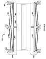
図1Aは、直視型マイクロ電気機械システム(MEMS)方式ディスプレイ装置100の概略図を示している。ディスプレイ装置100は、行および列に配列された複数の光変調器102a〜102d(全体として「光変調器102」)を含む。ディスプレイ装置100において、光変調器102aおよび102dは開状態にあり、光を通させる。光変調器102bおよび102cは閉状態にあり、光の通過を妨げる。光変調器102a〜102dの状態を選択的にセットすることによって、ディスプレイ装置100は、1つのランプまたは複数のランプ105で照射された場合、バックライト付きディスプレイ用の画像104を形成するのに利用することができる。別の実装形態では、装置100は、装置の前面から発する周辺光の反射によって、画像を形成することができる。別の実装形態では、装置100は、ディスプレイの前面に配置された1つのランプまたは複数のランプからの光の反射によって、すなわちフロントライトを使用して、画像を形成することができる。
FIG. 1A shows a schematic view of a direct-view micro-electromechanical system (MEMS)
いくつかの実装形態では、各光変調器102は、画像104中の画素106に対応する。いくつかの他の実装形態では、ディスプレイ装置100は、複数の光変調器を利用して、画像104中の画素106を形成することができる。たとえば、ディスプレイ装置100は、3つの色固有光変調器102を含み得る。特定の画素106に対応する色固有光変調器102のうちの1つまたは複数を選択的に開くことによって、ディスプレイ装置100は、画像104中のカラー画素106を生成することができる。別の例では、ディスプレイ装置100は、画像104中の輝度レベルを提供するために、画素106ごとに2つ以上の光変調器102を含む。画像に関して、「画素」は、画像の解像度によって定義される最も小さいピクチャ要素に対応する。ディスプレイ装置100の構造構成要素に関して、「画素」という用語は、画像の単一画素を形成する光を変調するのに使用される、機械構成要素と電気構成要素との組合せを指す。
In some implementations, each light modulator 102 corresponds to a
ディスプレイ装置100は、投影型アプリケーションで通常見出される結像光学素子を含まなくてよいという点で、直視型ディスプレイである。投影型ディスプレイでは、ディスプレイ装置の表面に形成される画像は、スクリーンまたは壁に投影される。ディスプレイ装置は、投影画像よりもかなり小さい。直視型ディスプレイでは、ユーザは、光変調器を含み、場合によってはディスプレイ上で見られる輝度および/またはコントラストを増強するためのバックライトまたはフロントライトを含むディスプレイ装置を直接見ることによって、画像を見る。
The
直視型ディスプレイは、透過モードまたは反射モードのいずれかで動作し得る。透過型ディスプレイでは、光変調器は、ディスプレイの後ろに配置された1つのランプまたは複数のランプから発する光をフィルタリングし、または選択的に遮断する。場合によっては、各画素を均一に照明できるように、ランプからの光は、光ガイドまたは「バックライト」に注入される。透過直視型ディスプレイは、光変調器を含む一方の基板がバックライトのすぐ上に配置されるサンドイッチアセンブリ配列を円滑にするように、透明基板またはガラス基板の上に構築されることが多い。 Direct view displays can operate in either transmissive mode or reflective mode. In a transmissive display, the light modulator filters or selectively blocks light emanating from a lamp or lamps located behind the display. In some cases, light from the lamp is injected into a light guide or “backlight” so that each pixel can be illuminated uniformly. Transmission direct view displays are often built on a transparent or glass substrate to facilitate a sandwich assembly arrangement in which one substrate containing a light modulator is placed directly above the backlight.
各光変調器102は、シャッター108および開口109を含むことができる。画像104中の画素106を照明するために、シャッター108は、見ている人に向かって光が開口109を通るように配置される。画素106を未点灯のまま保つために、シャッター108は、光が開口109を通過するのを妨げるように配置される。開口109は、各光変調器102中の反射材料または光吸収材料を通じてパターニングされた開放部によって画定される。
Each light modulator 102 can include a
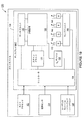
ディスプレイ装置は、シャッターの移動を制御するための、基板と、光変調器とに接続された制御マトリクスも含む。制御マトリクスは、画素の行ごとに、少なくとも1つの書込み許可相互接続110(「スキャンライン相互接続」とも呼ばれる)と、各画素列に対する1つのデータ相互接続112と、すべての画素に、または少なくとも、ディスプレイ装置100中の複数の列と複数の行の両方にある画素に共通電圧を与える1つの共通相互接続114とを含む、一連の電気相互接続(たとえば、相互接続110、112および114)を含む。適切な電圧(「書込み許可電圧、VWE」)の印加に応じて、所与の画素行に対する書込み許可相互接続110は、行中の画素を、新規シャッター移動命令を受諾するように準備する。データ相互接続112は、新規移動命令を、データ電圧パルスの形で伝達する。データ相互接続112に印加されるデータ電圧パルスは、いくつかの実装形態において、シャッターの静電的な移動に直接寄与する。いくつかの他の実装形態では、データ電圧パルスは、スイッチ、たとえばトランジスタ、または、データ電圧よりも通常、規模が高い別個の作動電圧の、光変調器102への印加を制御する他の非線形回路要素を制御する。次いで、これらの作動電圧を印加した結果、シャッター108の静電駆動移動が生じる。
The display device also includes a control matrix connected to the substrate and the light modulator for controlling the movement of the shutter. The control matrix includes, for each row of pixels, at least one write enable interconnect 110 (also referred to as a “scanline interconnect”), one
図1Bは、ホストデバイス(すなわち、セルフォン、スマートフォン、PDA、MP3プレーヤ、タブレット、電子リーダーなど)のブロック図120の一例を示している。ホストデバイスは、ディスプレイ装置128、ホストプロセッサ122、環境センサ124、ユーザ入力モジュール126、および電源を含む。
FIG. 1B shows an example of a block diagram 120 of a host device (ie, cell phone, smartphone, PDA, MP3 player, tablet, electronic reader, etc.). The host device includes a
ディスプレイ装置128は、複数のスキャンドライバ130(「書込み許可電圧源」とも呼ばれる)、複数のデータドライバ132(「データ電圧源」とも呼ばれる)、コントローラ134、共通ドライバ138、ランプ140〜146、およびランプドライバ148を含む。スキャンドライバ130は、スキャンライン相互接続110に書込み許可電圧を印加する。データドライバ132は、データ相互接続112にデータ電圧を印加する。
The
ディスプレイ装置のいくつかの実装形態において、データドライバ132は、特に画像104の輝度レベルがアナログ方式で導出されるべきである場合、光変調器にアナログデータ電圧を提供するように構成される。アナログ動作において、光変調器102は、ある範囲の中間電圧がデータ相互接続112を通して印加されると、シャッター108における、ある範囲の中間開状態が生じ、その結果、ある範囲の中間照明状態または画像104における輝度レベルが生じるように設計される。他の場合には、データドライバ132は、2つ、3つまたは4つのデジタル電圧レベルの縮小セットのみをデータ相互接続112に印加するように構成される。これらの電圧レベルは、デジタル方式で、シャッター108の各々に対して、開状態、閉状態、または他の個別の状態をセットするように設計される。
In some implementations of the display device, the data driver 132 is configured to provide an analog data voltage to the light modulator, particularly where the luminance level of the
スキャンドライバ130およびデータドライバ132は、デジタルコントローラ回路134(「コントローラ134」とも呼ばれる)に接続される。コントローラはデータを、行および画像フレームでグルーピングされた所定のシーケンスに編成されて、ほぼ直列方式でデータドライバ132に送る。データドライバ132は、直列並列データコンバータと、レベルシフティングと、一部のアプリケーション向けにはデジタルアナログ電圧コンバータとを含み得る。
The
ディスプレイ装置は、場合によっては、共通電圧源とも呼ばれる1組の共通ドライバ138を含む。いくつかの実装形態において、共通ドライバ138は、たとえば、一連の共通相互接続114に電圧を供給することによって、光変調器アレイ内のすべての光変調器にDC共通電位を提供する。いくつかの他の実装形態では、共通ドライバ138は、コントローラ134からのコマンドに従って、光変調器アレイに対し電圧パルスまたは信号、たとえば、アレイの複数の行および列中のすべての光変調器の同時作動を駆動および/または開始することが可能であるグローバル作動パルスを出す。
The display device includes a set of common drivers 138, sometimes referred to as a common voltage source. In some implementations, the common driver 138 provides a DC common potential to all light modulators in the light modulator array, for example, by supplying a voltage to a series of
異なるディスプレイ機能のためのドライバ(たとえば、スキャンドライバ130、データドライバ132、および共通ドライバ138)はすべて、コントローラ134によって時間同期される。コントローラからのタイミングコマンドが、ランプドライバ148と、画素アレイ内の特定の行の書込み許可およびシーケンシングと、データドライバ132からの電圧の出力と、光変調器作動を可能にする電圧の出力とにより、赤、緑および青および白色ランプ(それぞれ140、142、144、および146)の照明を調整する。
Drivers for different display functions (eg, scan
コントローラ134は、シャッター108の各々が、新規画像104に適した照明レベルにリセットされ得るためのシーケンシングまたはアドレス指定方式を決定する。新規画像104は、周期的間隔でセットされ得る。たとえば、ビデオディスプレイの場合、カラー画像104またはビデオフレームは、10〜300ヘルツ(Hz)の範囲の周波数でリフレッシュされる。いくつかの実装形態において、アレイへの画像フレームの設定は、交替画像フレームが、赤、緑および青など、交替する一連の色で照射されるように、ランプ140、142、144、および146の照明と同期される。それぞれの色のための画像フレームは、カラーサブフレームと呼ばれる。フィールド順次式カラー方法と呼ばれるこの方法では、カラーサブフレームが、20Hzを超過する周波数で交替される場合、人間の脳は、交替するフレーム画像を、広い連続する範囲の色を有する画像の知覚に平均する。代替実装形態では、原色をもつ4つ以上のランプが、ディスプレイ装置100において利用されてよく、赤、緑、および青以外の原色を利用する。
The
ディスプレイ装置100が、開状態と閉状態との間のシャッター108のデジタル切替えのために設計されるいくつかの実装形態において、コントローラ134は、前述のように、時分割グレースケールの方法によって画像を形成する。いくつかの他の実装形態では、ディスプレイ装置100は、画素ごとに複数のシャッター108を使用することによって、グレースケールを提供することができる。
In some implementations in which the
いくつかの実装形態において、画像状態104についてのデータは、コントローラ134によって、変調器アレイに、スキャンラインとも呼ばれる個々の行の順次アドレス指定によりロードされる。シーケンス中の行またはスキャンラインごとに、スキャンドライバ130は、アレイのその行について、書込み許可相互接続110に書込み許可電圧を印加し、続いて、データドライバ132が、選択された行中の各列について、所望のシャッター状態に対応するデータ電圧を供給する。このプロセスは、アレイ中のすべての行についてデータがロードされるまで繰り返す。いくつかの実装形態において、データローディングのための選択された行のシーケンスは、線形であり、アレイ中の上から下に進む。いくつかの他の実装形態では、選択された行のシーケンスは、視覚的アーティファクトを最小限にするために擬似ランダム化される。また、いくつかの他の実装形態では、シーケンシングはブロックで編成され、この場合、ブロックに対して、画像状態104の特定の一部のみについてのデータが、たとえば、シーケンス中のアレイの5行おきにのみアドレス指定することによってアレイにロードされる。
In some implementations, data about the
いくつかの実装形態において、アレイに画像データをロードするためのプロセスは、シャッター108を作動させるプロセスとは、時間的に分離される。これらの実装形態において、変調器アレイは、アレイ中の各画素に対するデータメモリ要素を含むことができ、制御マトリクスは、メモリ要素に記憶されたデータに従って、シャッター108の同時作動を開始するためのトリガ信号を、共通ドライバ138から搬送するためのグローバル作動相互接続を含み得る。
In some implementations, the process for loading image data into the array is separated in time from the process of actuating the
代替実装形態では、画素アレイと、画素を制御する制御マトリクスとが、方形の行および列以外の構成で配列され得る。たとえば、画素は、六角形アレイまたは曲線をなす行および列で配列され得る。概して、本明細書で使用するスキャンラインという用語は、書込み許可相互接続を共有する、任意の複数の画素を指すものである。 In an alternative implementation, the pixel array and the control matrix that controls the pixels may be arranged in configurations other than square rows and columns. For example, the pixels may be arranged in hexagonal arrays or curvilinear rows and columns. In general, the term scanline as used herein refers to any plurality of pixels that share a write-enabled interconnect.
ホストプロセッサ122は全般的に、ホストの動作を制御する。たとえば、ホストプロセッサは、ポータブル電子デバイスを制御するための汎用または専用プロセッサであり得る。ホストデバイス120内に含まれるディスプレイ装置128に対して、ホストプロセッサは、画像データならびにホストに関する追加データを出力する。そのような情報は、環境センサからのデータ、たとえば周辺光もしくは温度、ホストに関する情報、たとえば、ホストの動作モードもしくはホストの電源に残っている電力量、画像データの内容に関する情報、画像データのタイプに関する情報、および/または画像を選択する際に使用するディスプレイ装置に関する指示を含み得る。
The
ユーザ入力モジュール126は、ユーザの個人的好みをコントローラ134に直接、またはホストプロセッサ122を介して伝える。いくつかの実装形態では、ユーザ入力モジュールは、ユーザが「色をより濃く」、「コントラストをより良好に」、「電力をより低く」、「輝度を増して」、「スポーツ」、「ライブアクション」、または「アニメーション」などの個人的好みをプログラムしているソフトウェアによって制御される。いくつかの他の実装形態では、これらの好みは、スイッチまたはダイヤルなどのハードウェアを使用して、ホストに入力される。コントローラ134への複数のデータ入力はコントローラに対し、最適な画像化特性に対応する様々なドライバ130、132、138および148にデータを提供するように指示する。
The
環境センサモジュール124も、ホストデバイスの一部として含まれ得る。環境センサモジュールは、温度および/または周辺の採光条件など、周辺環境に関するデータを受信する。センサモジュール124は、デバイスが屋内またはオフィス環境で動作しているのか、明るい昼光の中の屋外環境で動作しているのか、夜間の屋外環境で動作しているのかを区別するようにプログラムされ得る。センサモジュールは、コントローラが周辺環境に応答して表示条件を最適化できるように、この情報をディスプレイコントローラ134に通信する。
An
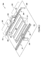
図2は、例示的なシャッター式光変調器200の透視図を示している。シャッター式光変調器は、図1Aの直視型MEMS方式ディスプレイ装置100への組込みに適している。光変調器200は、アクチュエータ204に結合されたシャッター202を含む。アクチュエータ204は、2つの別個のコンプライアント電極ビームアクチュエータ205(「アクチュエータ205」)から形成され得る。シャッター202は、一方では、アクチュエータ205に結合する。アクチュエータ205は、表面203に対して実質的に平行である運動面における表面203の上方で、シャッター202を横方向に移動する。シャッター202の反対側は、アクチュエータ204によって加えられる力に対向する復元力を与えるスプリング207に結合する。
FIG. 2 shows a perspective view of an exemplary shutter
各アクチュエータ205は、シャッター202をロードアンカ208に接続するコンプライアントロードビーム206を含む。ロードアンカ208は、コンプライアントロードビーム206とともに、機械的サポートとして働き、シャッター202を、表面203に近接して懸架されたまま保つ。表面は、光を通過させるための1つまたは複数の開口穴211を含む。ロードアンカ208は、コンプライアントロードビーム206とシャッター202とを表面203に物理接続し、ロードビーム206を、バイアス電圧、一部の事例ではグランドに電気接続する。
Each
基板がシリコンのような不透過性のものである場合、基板204を通して穴アレイをエッチングすることによって、基板に開口穴211が形成される。基板204がガラスやプラスチックのような透明なものである場合、基板203に堆積された遮光材料の層に開口穴211が形成される。開口穴211は概して、円形、楕円、多角形、蛇状、または形状が不規則でよい。
If the substrate is impermeable, such as silicon, etching the hole array through the
各アクチュエータ205は、各ロードビーム206に隣接して配置されたコンプライアント駆動ビーム216も含む。駆動ビーム216は、一方の端部において、駆動ビーム216の間で共有される駆動ビームアンカ218に結合する。各駆動ビーム216の他端は、自由に移動する。各駆動ビーム216は、駆動ビーム216の自由端と、ロードビーム206の固定端との近くで、ロードビーム206に最接近するように湾曲される。
Each
動作時、光変調器200を組み込むディスプレイ装置は、駆動ビームアンカ218を介して駆動ビーム216に電位を印加する。第2の電位が、ロードビーム206に印加され得る。駆動ビーム216とロードビーム206との間の得られる電位差は、駆動ビーム216の自由端を、ロードビーム206の固定端の方に引き付け、ロードビーム206のシャッター端を、駆動ビーム216の固定端の方に引き付け、そうすることによって、シャッター202を、駆動アンカ218に向かって横に駆動する。コンプライアント部材206は、ビーム206および216の電位にわたる電圧が除去されたとき、ロードビーム206がシャッター202をその初期位置に押し戻すように、スプリングとして働き、ロードビーム206に蓄えられた応力を解放する。
In operation, a display device incorporating
光変調器200などの光変調器は、電圧が除去された後にシャッターをその休止位置に戻すための、スプリングなどの受動復元力を組み込む。他のシャッターアセンブリは、「開」および「閉」アクチュエータの2種セット、ならびにシャッターを開状態または閉状態のいずれかに移動させるための「開」および「閉」電極の別個のセットを組み込むことができる。
Light modulators, such as
制御マトリクスによりシャッターおよび開口のアレイを制御して、画像が生じるようにし、多くの場合、適切な輝度レベルで画像を移動させるための様々な方法がある。一部のケースでは、制御は、ディスプレイの周囲にあるドライバ回路に接続された行および列相互接続の受動マトリクスアレイを用いて遂行される。他のケースでは、速度、ディスプレイの輝度レベルおよび/または電力消散性能を向上させるために、切替えおよび/またはデータ記憶要素を、アレイ(いわゆるアクティブマトリクス)の各画素中に含めることが適切である。 There are various ways to control the array of shutters and apertures through the control matrix to produce an image, and in many cases to move the image at the appropriate brightness level. In some cases, control is accomplished using a passive matrix array of row and column interconnects connected to driver circuitry around the display. In other cases, it is appropriate to include switching and / or data storage elements in each pixel of the array (so-called active matrix) in order to improve speed, display brightness level and / or power dissipation performance.
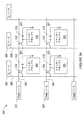
図3Aは、制御マトリクス300の例示的な概略図を示している。制御マトリクス300は、図1AのMEMS方式ディスプレイ装置100に組み込まれた光変調器を制御するのに適している。図3Bは、図3Aの制御マトリクス300に接続されたシャッター式光変調器アレイ320の透視図を示している。制御マトリクス300は、画素アレイ320(「アレイ320」)をアドレス指定することができる。各画素301は、アクチュエータ303によって制御される、図2のシャッターアセンブリ200などの弾性シャッターアセンブリ302を含み得る。各画素は、開口324を含む開口層322も含み得る。
FIG. 3A shows an exemplary schematic diagram of the
制御マトリクス300は、シャッターアセンブリ302が形成される基板304の表面に、拡散または薄膜堆積電気回路として組み立てられる。制御マトリクス300は、制御マトリクス300中の画素301の各行に対するスキャンライン相互接続306と、制御マトリクス300中の画素301の各列に対するデータ相互接続308とを含む。各スキャンライン相互接続306は、書込み許可電圧源307を、対応する画素301の行中の画素301に電気接続する。各データ相互接続308は、データ電圧源309(「Vdソース」)を、対応する画素の列中の画素301に電気接続する。制御マトリクス300中で、Vdソース309は、シャッターアセンブリ302の作動に使用されるエネルギーの大部分を提供する。このように、データ電圧源、Vdソース309は、作動電圧源としても働く。
The
図3Aおよび図3Bを参照すると、画素アレイ320中の各画素301または各シャッターアセンブリ302に対して、制御マトリクス300は、トランジスタ310とキャパシタ312とを含む。各トランジスタ310のゲートは、画素301が置かれているアレイ320中の行のスキャンライン相互接続306に電気接続される。各トランジスタ310のソースは、それに対応するデータ相互接続308に電気接続される。各シャッターアセンブリ302のアクチュエータ303は、2つの電極を含む。各トランジスタ310のドレインは、対応するキャパシタ312の1つの電極、および対応するアクチュエータ303の電極のうちの1つと並列に電気接続される。シャッターアセンブリ302内のキャパシタ312の他方の電極およびアクチュエータ303の他方の電極は、共通または接地電位に接続される。代替実装形態では、トランジスタ310は、半導体ダイオードおよび/または金属絶縁体金属サンドイッチ型スイッチ素子で置き換えることができる。
Referring to FIGS. 3A and 3B, for each
動作時、画像を形成するために、制御マトリクス300は、各スキャンライン相互接続306にVweを順に印加することによって、シーケンス中のアレイ320中の各行を書込み可能にする。書込み可能にされた行に対して、行中の画素301のトランジスタ310のゲートへのVweの印加により、トランジスタ310を通してデータ相互接続308に電流が流れて、シャッターアセンブリ302のアクチュエータ303に電位が印加される。行が書込み可能にされている間、データ電圧Vdが、データ相互接続308に選択的に印加される。アナロググレースケールを与える実装形態では、各データ相互接続308に印加されるデータ電圧は、書込み可能にされたスキャンライン相互接続306とデータ相互接続308との交差位置に置かれた画素301の所望の輝度との関係で変えられる。デジタル制御方式を提供する実装形態では、データ電圧は、比較的低規模の電圧(すなわち、グランドに近い電圧)になるように、またはVat(作動閾電圧)を満たし、もしくは超えるように選択される。データ相互接続308へのVatの印加に応答して、対応するシャッターアセンブリ内のアクチュエータ303が作動し、シャッターアセンブリ302内のシャッターを開く。データ相互接続308に印加された電圧は、制御マトリクス300が行にVweを印加するのをやめた後でも、画素301のキャパシタ312に蓄えられたまま留まる。したがって、シャッターアセンブリ302が作動するのに十分な程長い時間、行において電圧Vweを待ち、保持する必要はなく、そのような作動は、書込み許可電圧が行から除去された後も進行し得る。キャパシタ312は、アレイ320内のメモリ要素としても機能し、画像フレームの照明のために作動命令を記憶する。
In operation, in order to form an image, the
アレイ320の画素301ならびに制御マトリクス300は、基板304上に形成される。アレイは、基板304上に配設された開口層322を含み、開口層322は、アレイ320中のそれぞれの画素301に対する1組の開口324を含む。開口324は、各画素中のシャッターアセンブリ302と整列される。いくつかの実装形態では、基板304は、ガラスまたはプラスチックなどの透明材料から作られる。いくつかの他の実装形態では、基板304は、不透過性材料から作られるが、この場合、穴がエッチングされて開口324を形成する。
The
シャッターアセンブリ302は、アクチュエータ303とともに、双安定にされ得る。すなわち、シャッターは、いずれかの位置にシャッターを保持するための電力がほとんどまたはまったく要求されることなく、少なくとも2つの均衡位置(たとえば開または閉)に存在し得る。より具体的には、シャッターアセンブリ302は、機械的に双安定であり得る。シャッターアセンブリ302のシャッターが正しい位置でセットされると、その位置を維持するのに、電気エネルギーまたは保持電圧は要求されない。シャッターアセンブリ302の物理要素に対する機械的圧力が、シャッターを所定の場所で保持し得る。
The
シャッターアセンブリ302はまた、アクチュエータ303とともに、電気的に双安定にされ得る。電気的に双安定のシャッターアセンブリでは、シャッターアセンブリの作動電圧を下回る電圧範囲が存在し、この電圧範囲は、(シャッターが開または閉のいずれかの状態で)閉アクチュエータに印加されると、シャッターに対向力が加えられたとしても、アクチュエータを閉のまま、かつシャッターを所定の位置で保持する。対向力は、図2に示すシャッター式光変調器200内のスプリング207などのスプリングによって加えることができ、または対向力は、「開」もしくは「閉」アクチュエータなどの対向アクチュエータによって加えることができる。
The
光変調器アレイ320は、画素ごとに単一のMEMS光変調器を有するものとして示されている。各画素中に複数のMEMS光変調器が設けられる他の実装形態も可能であり、そうすることによって、各画素中の単なる2値の「オン」または「オフ」光学状態以上のものを可能にする。画素中の複数のMEMS光変調器が設けられ、光変調器の各々に関連付けられた開口324が不等面積をもつ符号化面積分割グレースケールのいくつかの形が可能である。
The
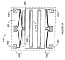
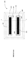
図4Aおよび図4Bは、二重アクチュエータシャッターアセンブリ400の例示的な図を示している。図4Aに示す二重アクチュエータシャッターアセンブリは、開状態にある。図4Bは、閉状態にある二重アクチュエータシャッターアセンブリ400を示している。シャッターアセンブリ200とは対照的に、シャッターアセンブリ400は、シャッター406の両側にアクチュエータ402および404を含む。各アクチュエータ402および404は、独立に制御される。第1のアクチュエータ、シャッター開アクチュエータ402は、シャッター406を開くのを担当する。第2の対向アクチュエータ、シャッター閉アクチュエータ404は、シャッター406を閉じるのを担当する。アクチュエータ402および404は両方とも、コンプライアントビーム電極アクチュエータである。アクチュエータ402および404は、シャッターがその上方で懸架されている開口層407に対して実質的に平行な平面にあるシャッター406を駆動することによって、シャッター406を開閉する。シャッター406は、アクチュエータ402および404に取り付けられたアンカ408によって、開口層407の上方で小さな間隔で懸架される。シャッター406の移動軸に沿って、シャッター406の両端に取り付けられたサポートを含むことにより、シャッター406の面外運動が低減され、運動が基板に対して実質的に平行な平面へ閉じ込められる。図3Aの制御マトリクス300との類似性によって、シャッターアセンブリ400とともに使用するのに適した制御マトリクスは、対向するシャッター開アクチュエータ402およびシャッター閉アクチュエータ404の各々につき、1つのトランジスタおよび1つのキャパシタを含み得る。
4A and 4B show exemplary views of a dual
シャッター406は、光が通り得る2つのシャッター開口412を含む。開口層407は、3つの開口409からなるセットを含む。図4Aにおいて、シャッターアセンブリ400は開状態にあり、したがって、シャッター開アクチュエータ402は作動しており、シャッター閉アクチュエータ404はその弛緩位置にあり、シャッター開口412の中心線が開口層の開口409のうちの2つの中心線と一致する。図4Bにおいてシャッターアセンブリ400は閉状態に移されており、したがって、シャッター開アクチュエータ402はその弛緩位置にあり、シャッター閉アクチュエータ404は作動しており、シャッター406の遮光部分はこの場合、開口409(点線として示す)を通る光の透過を遮断するための所定の位置にある。
The
各開口は、その周囲に、少なくとも1つの辺をもつ。たとえば、方形開口409は、4つの辺をもつ。円形、楕円、卵型、または他の湾曲開口が開口層407に形成される代替実装形態では、各開口は、単一辺のみを有し得る。いくつかの他の実装形態では、開口は、数学的な意味において分離され、または独立する必要はなく、連結されてよい。すなわち、開口の一部または成形断面が、各シャッターとの対応を維持し得る間、これらのセクションのいくつかは、開口の単一の連続外周が複数のシャッターによって共有されるように連結され得る。
Each opening has at least one side around it. For example, the
様々な出口角をもつ光を、開状態にある開口412および409に通すために、開口層407中の開口409の対応する幅またはサイズよりも大きい幅またはサイズをシャッター開口412に与えることが有利である。閉状態において光が漏れるのを効果的に阻止するために、シャッター406の遮光部分が開口409と重なるのが好ましい。図4Bは、シャッター406内の遮光部分の辺と、開口層407内に形成される開口409の1つの辺との間の所定の重複416を示す。
It is advantageous to provide the
静電アクチュエータ402および404は、その電圧変位挙動により、シャッターアセンブリ400に双安定特性が与えられるように設計される。シャッター開アクチュエータおよびシャッター閉アクチュエータの各々について、作動電圧を下回る電圧範囲が存在し、この電圧範囲は、そのアクチュエータが閉状態である(シャッターは開または閉のいずれかである)間に印加されると、対向アクチュエータに作動電圧が印加された後でも、アクチュエータを閉じたまま、かつシャッターを所定の位置に保持する。そのような対向力に対してシャッターの位置を維持するのに必要とされる最小電圧は、維持電圧Vmと呼ばれる。
The
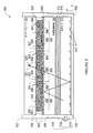
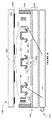
図5は、シャッター式光変調器(シャッターアセンブリ)502を組み込むディスプレイ装置500の例示的な断面図を示している。各シャッターアセンブリは、シャッター503とアンカ505とを組み込む。アンカ505とシャッター503との間で接続されると、表面の上で短い距離でシャッターを懸架するのを助けるコンプライアントビームアクチュエータについては図示していない。シャッターアセンブリ502は、好ましくはプラスチックまたはガラスで作られた、透明基板504上に配設される。基板504上に配設された後ろ向き反射開口層506が、シャッターアセンブリ502のシャッター503の閉位置の下に置かれた複数の表面開口508を画定する。反射開口層506は、表面開口508を通らない光を、ディスプレイ装置500の後ろに向かって反射して戻す。反射開口層506は、スパッタリング、蒸着、イオンプレーティング、レーザアブレーション、または化学気相堆積を含む多数の堆積技法によって薄膜方式で形成された含有物をもたない微粒金属膜であり得る。いくつかの実装形態では、反射開口層506は、誘電鏡などの鏡から形成され得る。誘電鏡は、高および低屈折率の材料を交互に繰り返す誘電薄膜の積層として組み立てられ得る。シャッターが自由に移動する反射開口層506からシャッター503を分離する垂直ギャップは、0.5〜10ミクロンの範囲内である。垂直ギャップの規模は、図4Bに示す重複416など、閉状態における、シャッター503の辺と、開口508の辺との間の横の重複よりも小さいのが好ましい。
FIG. 5 shows an exemplary cross-sectional view of a
ディスプレイ装置500は、基板504を平面光ガイド516から分離する随意のディフューザ512および/または随意の輝度増強膜514を含む。光ガイドは、透明材料、すなわちガラス材料またはプラスチック材料を含む。光ガイド516は、1つまたは複数の光源518によって照射され、バックライト515を形成する。光源518は、たとえば、限定はしないが、白熱電球、蛍光灯、レーザ、または発光ダイオード(LED)(全体的に「ランプ」と呼ぶ)でよい。反射体519は、光源518から光ガイド516に光を向けるのを助ける。前向き反射膜520が、バックライト515の後ろに配設され、シャッターアセンブリ502に向かって光を反射する。シャッターアセンブリ502のうちの1つを通らない、バックライト515からの光線521などの光線は、バックライト515に戻され、膜520から再度反射される。この方式において、第1のパス上に画像を形成するためにディスプレイを離れることができない光は、リサイクルし、シャッターアセンブリアレイ502中の他の開いた開口の透過のために利用可能にすることができる。そのような光リサイクルは、ディスプレイの照明効率を上げることがわかっている。
The
光ガイド516は、光源518から開口508の方に、したがってディスプレイの前面の方に光を向け直す1組の幾何学的光リダイレクタまたはプリズム517を含む。光リダイレクタは、代替可能に断面が三角形、台形になる、または湾曲することができる形状をもつ光ガイド516のプラスチック本体内に成形することができる。プリズム517の密度は概して、光源518からの距離とともに増大する。
The light guide 516 includes a set of geometric light redirectors or
いくつかの実装形態では、開口層506は、光吸収材料で作ることができ、代替実装形態では、シャッター503の表面は、光吸収材料または光反射材料のいずれかでコーティングすることができる。いくつかの他の実装形態では、開口層506は、光ガイド516の表面に直接堆積され得る。いくつかの実装形態では、開口層506は、(後で説明するMEMSダウン構成の場合のように)シャッター503およびアンカ505と同じ基板上に配設される必要はない。
In some implementations, the
いくつかの実装形態では、光源518は、異なる色、たとえば、赤、緑、および青色のランプを含み得る。人間の脳が、異なる色の画像を単一の多色画像に平均するのに十分なレートで、異なる色のランプで画像を連続して照明することによって、カラー画像が形成され得る。様々な色固有画像が、シャッターアセンブリアレイ502を使って形成される。別の実装形態では、光源518は、3つよりも多い異なる色をもつランプを含む。たとえば、光源518は、赤、緑、青および白色ランプまたは赤、緑、青および黄色ランプを有し得る。いくつかの他の実装形態では、光源518は、シアン、マゼンタ、黄色および白色ランプまたは赤、緑、青および白色ランプを含み得る。いくつかの他の実装形態では、追加のランプが光源に含まれ得る。たとえば、5つの色を使用する場合、光源は、赤、緑、青、シアンおよび黄色ランプを含み得る。いくつかの他の実装形態では、光源518は、白、オレンジ、青、紫および緑色ランプまたは白、青、黄色、赤およびシアン色ランプを含み得る。6つの色を使用する場合、光源は、赤、緑、青、シアン、マゼンタおよび黄色ランプまたは白、シアン、マゼンタ、黄色、オレンジおよび緑色ランプを含み得る。
In some implementations, the
カバープレート522は、ディスプレイ装置500の前面を形成する。カバープレート522の後ろ側は、コントラストを増すために、ブラックマトリクス524でカバーされ得る。代替実装形態では、カバープレートは、カラーフィルタ、たとえば、シャッターアセンブリ502のうちの異なるものに対応する、固有の赤、緑、および青フィルタを含む。カバープレート522は、シャッターアセンブリ502から所定の距離だけ離れて支えられ、ギャップ526を形成する。ギャップ526は、機械的サポートもしくはスペーサ527によって、かつ/またはカバープレート522を基板504に付着させる粘着シール528によって維持される。
The cover plate 522 forms the front surface of the
粘着シール528は、流体530を封じ込める。流体530は、好ましくは約10センチポアズを下回る粘度、好ましくは約2.0を上回る比誘電率、および約104V/cmを上回る誘電破壊強度で作製される。流体530は、潤滑油としても働き得る。いくつかの実装形態では、流体530は、高い表面濡れ性をもつ疎水性液体である。代替実装形態では、流体530は、基板504の屈折率よりも大きい、または小さい屈折率をもつ。
機械的光変調器を組み込むディスプレイは、数百、数千、または場合によっては数百万の可動要素を含み得る。いくつかのデバイスでは、要素が移動するたびに、静止摩擦が要素のうちの1つまたは複数を無効にする機会が生じる。この移動は、(流体530とも呼ばれる)流体にすべての部品を浸漬し、MEMSディスプレイセルの流体空間またはギャップ内に(たとえば接着剤で)流体を密閉することによって、促進される。流体530は通常、摩擦係数が低く、粘度が低く、長期的に劣化の影響が最小である。MEMS方式ディスプレイアセンブリが流体530用に液体を含むとき、液体は少なくとも部分的に、MEMS方式光変調器の可動部のうちのいくつかを囲む。いくつかの実装形態では、作動電圧を下げるために、液体は、70センチポアズを下回る粘度を有する。いくつかの他の実装形態では、液体は、10センチポアズを下回る粘度を有する。70センチポアズを下回る粘度を有する液体は、4,000グラム/モルを下回るか、または場合によっては400グラム/モルを下回る低分子量を有する材料を含み得る。そのような実装形態に好適であり得る流体530は、限定はしないが、脱イオン水、メタノール、エタノールおよび他のアルコール、パラフィン、オレフィン、エーテル、シリコーンオイル、フッ化シリコーンオイル、または他の天然もしくは合成の溶剤もしくは潤滑油を含む。有用な流体は、ポリジメチルシロキサン(PDMS)、たとえば、ヘキサメチルジシロキサンおよびオクタメチルトリシロキサン、またはアルキルメチルシロキサン、たとえば、ヘキシルペンタメチルジシロキサンであり得る。有用な流体はアルカン、たとえば、オクタンまたはデカンであり得る。有用な流体はニトロアルカン、たとえば、ニトロメタンであり得る。有用な流体は芳香族化合物、たとえば、トルエンまたはジエチルベンゼンであり得る。有用な流体はケトン、たとえば、ブタノンまたはメチルイソブチルケトンであり得る。有用な流体はクロロカーボン、たとえば、クロロベンゼンであり得る。有用な流体はクロロフルオロカーボン、たとえば、ジクロロフルオロエタンまたはクロロトリフルオロエチレンであり得る。これらのディスプレイアセンブリについて考えられる他の流体には、酢酸ブチル、ジメチルホルムアミドが含まれる。これらのディスプレイアセンブリについてのさらに他の有用な流体には、ハイドロフルオロエーテル、パーフルオロポリエーテル、ハイドロフルオロポリエーテル、ペンタノール、およびブタノールが含まれる。例示的な適切なハイドロフルオロエーテルには、エチルノナフルオロブチルエーテルおよび2-トリフルオロメチル-3-エトキシドデカフルオロヘキサンが含まれる。
Displays that incorporate mechanical light modulators can include hundreds, thousands, or even millions of movable elements. In some devices, each time the element moves, there is an opportunity for static friction to invalidate one or more of the elements. This movement is facilitated by immersing all parts in a fluid (also referred to as fluid 530) and sealing the fluid (eg, with an adhesive) within the fluid space or gap of the MEMS display cell.
薄板金属または成形プラスチックアセンブリブラケット532は、カバープレート522と、基板504と、バックライト515と、他の構成要素部とを合わせて、辺の周りに保持する。アセンブリブラケット532は、複合ディスプレイ装置500に剛性を加えるために、ねじまたは刻みタブで取り付けられる。いくつかの実装形態において、光源518は、エポキシポッティング化合物によって、所定の場所に成形される。反射体536は、光ガイド516の辺から漏れた光を光ガイドに戻すのを助ける。シャッターアセンブリ502および光源518に制御信号ならびに電力を与える電気相互接続は、図5に示していない。
The sheet metal or molded
ディスプレイ装置500は、MEMSアップ構成と呼ばれ、MEMS方式光変調器が、基板504の前面、すなわち見ている人の方を向く表面に形成される。シャッターアセンブリ502は、反射開口層506のすぐ上に構築される。MEMSダウン構成と呼ばれる代替実装形態において、シャッターアセンブリは、反射開口層が形成される基板とは別個の基板上に配設される。複数の開口を画定する反射開口層が形成される基板は、本明細書では、開口プレートと呼ばれる。MEMSダウン構成において、MEMS方式光変調器を積載する基板は、ディスプレイ装置500におけるカバープレート522に取って代わり、上部基板の後面、すなわち見ている人に背を向けて、バックライト516の方を向く表面にMEMS方式光変調器が配置されるように配向される。MEMS方式光変調器は、そうすることによって、反射開口層506にあるギャップに直接対向して、かつギャップにわたって配置される。ギャップは、開口プレートと、MEMS変調器が形成される基板とを接続する一連のスペーサポストによって維持することができる。いくつかの実装形態において、スペーサは、アレイ中の各画素内に、または各画素の間に配設される。MEMS光変調器を、それに対応する開口から分離するギャップまたは距離は、好ましくは10ミクロン未満、または重複416など、シャッターと開口との間の重複よりも小さい距離である。
The
図6A〜図6Eは、例示的な合成シャッターアセンブリの構築の段階の断面図を示している。図6Aは、完成された合成シャッターアセンブリ600の例示的な断面図を示している。シャッターアセンブリ600は、シャッター601、2つのコンプライアントビーム602、ならびに基板603および開口層606の上に構築されたアンカ構造体604を含む。合成シャッターアセンブリ600の要素は、第1の機械層605、導体層607、第2の機械層609、および封入誘電体611を含む。機械層の一方または両方は、シャッターアセンブリ600の主要ロードベアリングおよび機械的作動部材として働くので、機械層605または609のうちの少なくとも1つは、0.15ミクロンを上回る厚さで堆積され得るが、いくつかの実装形態では、機械層605および609はより薄い場合がある。機械層605および609の材料の候補として、限定はしないが、金属、たとえばアルミニウム(Al)、銅(Cu)、ニッケル(Ni)、クロム(Cr)、モリブデン(Mo)、チタン(Ti)、タンタル(Ta)、ニオブ(Nb)、ネオジム(Nd)、もしくはそれらの合金、誘電体材料、たとえば酸化アルミニウム(Al2O3)、酸化ケイ素(SiO2)、五酸化タンタル(Ta2O5)、もしくは窒化ケイ素(Si3N4)、または半導体材料、たとえばダイヤモンドライクカーボン、ケイ素(Si)、ゲルマニウム(Ge)、ガリウムヒ素(GaAs)、テルル化カドミウム(CdTe)もしくはそれらの合金が含まれる。導体層607などの層のうちの少なくとも1つは、作動要素との間で電荷を授受するように導電性であるべきである。材料の候補として、限定はしないが、Al、Cu、Ni、Cr、Mo、Ti、Ta、Nb、Ndもしくはそれらの合金、または半導体材料、たとえば、ダイヤモンドライクカーボン、Si、Ge、GaAs、CdTeもしくはそれらの合金がある。いくつかの実装形態では、半導体層を用いて、半導体にリン(P)、ヒ素(As)、ホウ素(B)、またはアルミニウム(Al)などの不純物をドープする。図6Aは、同様の厚さおよび機械的特性を有する機械層605および609が導体層607の両側に堆積された合成物のサンドイッチ構成を示している。いくつかの実装形態では、サンドイッチ構造は、堆積後に残っている応力および/または温度変動によって課せられる応力がシャッターアセンブリ600の曲げ、反りまたは他の変形を引き起こさないようにするのを助ける。
6A-6E show cross-sectional views of stages in the construction of an exemplary synthetic shutter assembly. FIG. 6A shows an exemplary cross-sectional view of the completed
いくつかの実装形態では、シャッターの外側が導電層から形成される一方、シャッターの内側が機械層から形成されるように、合成シャッターアセンブリ600における層の順序は逆になってよい。
In some implementations, the order of the layers in the
シャッターアセンブリ600は、封入誘電体611を含み得る。いくつかの実装形態では、シャッターおよびビームのすべての下面、上面および側面が均一にコーティングされるように、誘電体コーティングはコンフォーマルに適用されてよい。そのような薄膜は、熱酸化によって、かつ/または酸化アルミニウム(Al2O3)、酸化クロム(III)(Cr2O3)、酸化チタン(TiO2)、酸化ハフニウム(HfO2)、酸化バナジウム(V2O5)、酸化ニオブ(Nb2O5)、五酸化タンタル(Ta2O5)、酸化ケイ素(SiO2)もしくは窒化ケイ素(Si3N4)などの絶縁体のコンフォーマルコンフォーマル化学気相堆積によって、または原子層堆積を通じて同様の材料を堆積することによって成長し得る。誘電体コーティング層は、10nm〜1ミクロンの範囲内の厚さで加えられ得る。いくつかの実装形態では、誘電体コーティングを側壁に堆積するために、スパッタリングおよび蒸着が使用され得る。
The
図6B〜図6Eは、図6に示すシャッターアセンブリ600を形成するために使用される例示的なプロセスのいくつかの中間製造段階の結果の例示的な断面図を示している。いくつかの実装形態では、シャッターアセンブリ600は、図3Aおよび図3Bに示す制御マトリクスのような薄膜トランジスタのアクティブマトリクスアレイなどの既存の制御マトリクスの上に構築される。
6B-6E illustrate exemplary cross-sectional views resulting from several intermediate manufacturing steps of the exemplary process used to form the
図6Bは、シャッターアセンブリ600を形成する例示的なプロセスにおける第1の段階の結果の断面図を示している。図6Bに示すように、犠牲層613が堆積され、パターニングされる。いくつかの実装形態では、犠牲材料としてポリイミドが使用される。他の犠牲材料の候補として、ポリマー材料、たとえばポリアミド、フルオロポリマー、ベンゾシクロブテン、ポリフェニルキノキシレン、パリレン、またはポリノルボルネンがある。これらの材料は、粗い表面を平坦化し、250℃を上回る処理温度で機械的完全性を維持する能力、ならびにエッチングおよび/または除去中の熱分解の容易さを理由に選ばれる。他の実装形態では、犠牲層613は、ポリ酢酸ビニル、ポリビニルエチレンおよびフェノール樹脂またはノボラック樹脂などのフォトレジストから形成される。いくつかの実装形態で使用される代替犠牲層材料としてSiO2があり、これは、その除去に使用されるフッ化水素酸溶液に対して他の電子層または構造層が耐性を有する限り、優先的に除去され得る。1つのそのような適した耐性材料として、Si3N4がある。別の代替犠牲層材料としてSiがあり、これは、大半の金属およびSi3N4など、その除去に使用されるフッ素プラズマまたはフッ化キセノン(XeF2)に対して他の電子層および構造層が耐性を有する限り、優先的に除去され得る。さらに別の代替犠牲層材料としてAlがあり、これは、濃縮水酸化ナトリウム(NaOH)溶液など、強力なアルカリ溶液に対して他の電子層または構造層が耐性を有する限り、優先的に除去され得る。適した材料には、たとえば、Cr、Ni、Mo、TaおよびSiがある。さらに別の代替犠牲層材料としてCuがあり、これは、硝酸溶液または硫酸溶液に対して他の電子層または構造層が耐性を有する限り、優先的に除去され得る。そのような材料には、たとえば、Cr、Ni、およびSiがある。
FIG. 6B shows a cross-sectional view of the results of the first stage in an exemplary process for forming the
次に犠牲層613は、アンカ領域604に穴またはビアを露出させるようにパターニングされる。ポリイミドまたは他の非感光性材料を犠牲層材料として用いる実装形態では、犠牲層材料は感光剤を含むように作られてよく、それにより、UVフォトマスクを通じて露光された領域を現像液中で優先的に除去することができる。他の材料から形成された犠牲層は、フォトレジストの追加層において犠牲層613をコーティングし、フォトレジストをフォトパターニングし、最後にフォトレジストをエッチングマスクとして使用することによってパターニングされ得る。犠牲層613は、代替的に、SiO2またはCrなどの金属の薄層であり得るハードマスクにより犠牲層613をコーティングすることによってパターニングされ得る。次いでフォトパターンが、フォトレジストおよび湿式化学エッチングによってハードマスクに転写される。ハードマスクに現像されるパターンは、非常に深くて狭いアンカ穴を犠牲層613に与えるために使用され得る乾式化学エッチング技法、異方性エッチング技法、またはプラズマエッチング技法に対して非常に耐性があり得る。
The
アンカ領域604が犠牲層613中に開かれた後、表面の酸化物層を除去するために、露出した下にある導電面614を化学的に、またはプラズマのスパッタリング効果によってエッチングすることができる。そのようなコンタクトエッチング段階により、下にある導体とシャッター材料とのオーム接触を改善することができる。犠牲層のパターニングの後、フォトレジスト層またはハードマスクが、溶剤洗浄法または酸エッチング法のいずれかを使用して除去され得る。
After the
次に、図6Cに示すように、シャッターアセンブリ600を構築するためのプロセスにおいて、シャッター材料が堆積される。シャッターアセンブリ600は、複数の薄膜、すなわち第1の機械層605、導体層607および第2の機械層609から構成される。いくつかの実装形態では、第1の機械層605はアモルファスシリコン(a-Si)層であり、導体層607はAlであり、第2の機械層609はa-Siである。第1の機械層605、導体層607および第2の機械層609は、犠牲層613に物理的劣化が生じる温度を下回る温度で堆積される。たとえば、ポリイミドは約400℃を上回る温度で分解する。したがって、いくつかの実装形態では、第1の機械層605、導体層607および第2の機械層609は、400℃を下回る温度で堆積され、ポリイミドを犠牲材料として使用することを可能にする。いくつかの実装形態では、水素化アモルファスシリコン(a-Si:H)は、約250〜350℃の範囲の温度でシランガスからプラズマ支援化学気相成長法(PECVD)によって、応力が比較的少ない状態において、約0.15〜3ミクロンの範囲の厚さに成長可能であるので、第1の機械層605および第2の機械層609にとって有用な機械材料である。そのような実装形態のうちのいくつかでは、a-Siが約1オームcmを下回る抵抗率で成長し得るように、ドーパントとしてホスフィンガス(PH3)が使用される。代替実装形態では、同様のPECVD技法が、第1の機械層605としてSi3N4、シリコンリッチなSi3N4もしくはSiO2材料の堆積に、または第1の機械層605のためにダイヤモンドライクカーボン、Ge、SiGe、CdTeもしくは他の半導体材料の堆積に使用され得る。PECVD堆積技法の利点として、堆積が非常にコンフォーマルになり得る、すなわち、様々な傾斜面または狭いビアホールの内面をコーティングし得る。犠牲材料に切り込まれたアンカまたはビアホールがほぼ垂直な側壁を呈しているとしても、PECVD技法は、アンカの下水平面と上水平面との間に連続したコーティングを実現することができる。
Next, as shown in FIG. 6C, shutter material is deposited in a process for constructing the
PECVD技法に加えて、第1の機械層605および第2の機械層609の成長のために利用可能な代替の適した技法には、RFまたはDCスパッタリング、金属有機化学気相成長法、蒸着、電気めっきまたは無電解めっきが含まれる。
In addition to PECVD techniques, alternative suitable techniques available for the growth of first
導電層607には、いくつかの実装形態では、Alなどの金属薄膜が利用される。いくつかの他の実装形態では、Cu、Ni、Mo、またはTaなどの代替金属が選択され得る。そのような導電性材料を含めることは、2つの目的を果たす。それは、シャッター601の全体的なシート抵抗を軽減するほか、a−Siは、シャッター601のいくつかの実装形態で使用され得るように、2ミクロン未満の厚さである場合に、可視光をある程度透過し得るので、シャッター601を可視光が通るのを妨げるのを助ける。導電性材料は、スパッタリングによって、またはよりコンフォーマルに、化学気相堆積技法、電気めっきもしくは無電解めっきによって、堆積され得る。
In some implementations, a thin metal film such as Al is used for the
図6Dは、シャッターアセンブリ600の形成に使用される次の1組の処理段階の結果を示している。第1の機械層605、導電層607、および第2の機械層609がフォトマスクされ、エッチングされる一方、犠牲層613は依然として基板603上にある。第1に、フォトレジスト材料が施され、次いでフォトマスクを通して露光され、次いで現像されてエッチマスクが形成される。次いでアモルファスシリコン、Si3N4、およびSiOが、フッ素ベースのプラズマ化学でエッチングされ得る。SiO2機械層はまた、HF湿式化学を使用してエッチングでき、導電層607におけるいずれの金属も、湿式化学または塩素ベースのプラズマ化学反応のいずれかを使用してエッチングできる。
FIG. 6D shows the result of the next set of processing steps used to form the
フォトマスクを通じて付与されるパターン形状は、シャッターアセンブリ600のアクチュエータおよびシャッター601における剛性、コンプライアンス、電圧応答などの機械的特性に影響を及ぼす。シャッターアセンブリ600は、断面で示すコンプライアントビーム602を含む。コンプライアントビーム602は、幅がシャッター材料の全体的な高さまたは厚さを下回るように形成される。いくつかの実装形態では、ビーム寸法比は1.4:1以上に、コンプライアントビーム602が幅よりも高くまたは厚くなるように維持される。
The pattern shape imparted through the photomask affects mechanical properties such as rigidity, compliance, voltage response, etc., in the actuator of the
シャッターアセンブリ600を構築するための例示的な製造プロセスの後続段階の結果が、図6Eに示されている。犠牲層613が除去されて、アンカポイントを除いて基板603からすべての可動部が解放される。いくつかの実装形態では、ポリイミド犠牲材料が酸素プラズマにおいて除去される。犠牲層613に使用された他のポリマー材料も、酸素プラズマにおいて、または場合によっては熱分解によって除去され得る。いくつかの犠牲層材料(SiO2など)は、湿式化学エッチングによって、または気相エッチングによって除去され得る。
The result of subsequent steps of an exemplary manufacturing process for constructing the
図6Aに結果が示されている最終プロセスにおいて、封入誘電体611がシャッター601のすべての露出面に堆積される。いくつかの実装形態では、シャッター601およびビーム602のすべての下面、上面および側面が化学気相堆積を使用して均一にコーティングされるように、封入誘電体611はコンフォーマルに施されてよい。いくつかの他の実装形態では、シャッター601の上面および側面のみがコーティングされる。いくつかの実装形態では、Al2O3が封入誘電体611に使用され、約10〜約100ナノメートルの範囲内の厚さで原子層堆積によって堆積される。
In the final process, the results of which are shown in FIG. 6A, an encapsulating
最後に、反スティクションコーティングがシャッター601およびビーム602の表面に施され得る。これらのコーティングは、アクチュエータの2つの独立したビーム間の不要な貼り付きまたは粘着を防止する。適したコーティングは、炭素膜(グラファイトとダイヤモンド状の両方)ならびにフルオロポリマーおよび/または低蒸気圧潤滑油ならびにクロロシラン、炭化水素クロロシラン、フッ化炭素クロロシラン、たとえばメトキシ終端化シラン、パーフルオロ化、アミノシラン、シロキサンおよびカルボン酸ベースのモノマーおよび化学種を含む。これらのコーティングは、分子蒸気への露出、または化学気相堆積による前駆体化合物の分解のいずれかによって施され得る。スティクション防止コーティングは、絶縁表面のフッ化、シラン化、シロキサン化、または水素化におけるような、シャッター表面の化学変換によって作成されてもよい。
Finally, an anti-stiction coating can be applied to the surfaces of
MEMS方式シャッターディスプレイにおいて使用するのに適したアクチュエータの種類の1つとして、ディスプレイ基板に対して横であるか、またはディスプレイ基板の面内であるシャッター運動を制御するためのコンプライアントアクチュエータビームが含まれる。そのようなシャッターアセンブリの作動に用いられる電圧は、アクチュエータビームがよりコンプライアントになるにつれて低下する。作動している運動の制御はまた、面外運動に対して面内運動が優先または促進されるようにビームが形成される場合に改善する。それによって、いくつかの実装形態では、コンプライアントアクチュエータビームは、ビームが幅よりも高くまたは厚くなるような方形断面を有する。 One type of actuator suitable for use in a MEMS shutter display includes a compliant actuator beam for controlling shutter motion that is lateral to or in the plane of the display substrate. It is. The voltage used to operate such a shutter assembly decreases as the actuator beam becomes more compliant. Control of motion in motion also improves when the beam is formed such that in-plane motion is prioritized or promoted over out-of-plane motion. Thereby, in some implementations, the compliant actuator beam has a rectangular cross-section such that the beam is higher or thicker than it is wide.
特定の平面内の曲げに対する長い方形ビームの剛性は、その平面におけるそのビームの最も薄い寸法の3乗に比例する。したがって、面内運動の作動電圧を下げるためにコンプライアントビームの幅を縮小することは有利である。しかしながら、従来型のフォトリソグラフィ機器を使用してシャッターおよびアクチュエータ構造体を画定し、組み立てるとき、ビームの最小幅は光学素子の解像度に限定され得る。そして、15ナノメートルという狭い特徴体によりフォトレジストにおいてパターンを画定するようにフォトリソグラフィ機器が開発されてきたものの、そのような機器は高価であり、単一の露出においてパターニングが達成され得るエリアは限られている。ガラスの大型パネルでの経済的フォトリソグラフィでは、パターニング解像度または最小特徴体サイズは通常、1ミクロンまたは2ミクロン以上に限定される。 The rigidity of a long square beam against bending in a particular plane is proportional to the cube of the thinnest dimension of that beam in that plane. Therefore, it is advantageous to reduce the width of the compliant beam in order to reduce the operating voltage for in-plane motion. However, when using conventional photolithographic equipment to define and assemble the shutter and actuator structure, the minimum width of the beam can be limited to the resolution of the optical element. And while photolithography equipment has been developed to define patterns in photoresist with narrow features of 15 nanometers, such equipment is expensive and the area where patterning can be achieved with a single exposure is limited. For economical photolithography on large panels of glass, the patterning resolution or minimum feature size is usually limited to 1 micron or 2 microns or more.
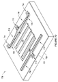
図7A〜図7Dは、狭い側壁ビームを有する例示的なシャッターアセンブリ700の構築の段階の等角図である。この代替プロセスは、コンプライアントアクチュエータビーム718および720ならびにコンプライアントスプリングビーム716(「側壁ビーム716、718および720」と総称される)をもたらし、側壁ビーム716、718および720の幅は、大きいガラスパネルに対する従来型のリソグラフィの限度を大きく下回る。図7A〜図7Dに示すプロセスでは、シャッターアセンブリ700のコンプライアントビームは、犠牲材料から作られる型上の側壁特徴体として形成される。このプロセスは側壁ビームプロセスと呼ばれる。
7A-7D are isometric views of the stages of construction of an
側壁ビーム716、718および720を有するシャッターアセンブリ700を形成するプロセスは、図7Aに示すように、第1の犠牲材料701の堆積およびパターニングで始まる。第1の犠牲材料において画定されるパターンは、開口またはビア702を作り、最終的には開口またはビア702の中に、シャッターのアンカが形成される。第1の犠牲材料701の堆積およびパターニングは、図6A〜図6Eに関して説明した堆積およびパターニングについて述べたものと概念的に類似しており、類似の材料を使用する。
The process of forming the
側壁ビーム716、718および720を形成するプロセスは、第2の犠牲材料705の堆積およびパターニングで続く。図7Bは、第2の犠牲材料705のパターニング後に作られた型703の形状を示している。型703はまた、第1の犠牲材料701およびその以前に画定されたビア702を含む。図7Bにおける型703は、2つの別個の水平レベルを含む。型703の下水平レベル708は、第1の犠牲材料701の上面によって確立されており、第2の犠牲層705がエッチング除去されているエリアにおいてアクセス可能である。型703の上水平レベル710は、第2の犠牲層705の上面によって確立されている。図7Bに示す型703はまた、実質的に垂直な側壁709を含む。
The process of forming
第1の犠牲層701および第2の犠牲層705として使用するための材料は、図6A〜図6Eの犠牲層613に関して上述している。
Materials for use as the first
側壁ビーム716、718および720を形成するプロセスは、図7Cに示すように、型703の露出面のすべてへのシャッター材料の堆積およびパターニングで続く。シャッター712を形成する際に使用するのに適した材料については、図6A〜図6Eの第1の機械層605、導電層607、および第2の機械層609に関して上述している。シャッター材料は、約2ミクロン未満の厚さで堆積される。いくつかの実装形態では、シャッター材料は、約1.5ミクロン未満の厚さを有するように堆積される。いくつかの他の実装形態では、シャッター材料は、約1.0ミクロン未満の厚さを有するように、また約0.10ミクロンほどの薄さで堆積される。堆積後、シャッター材料(上述したように、いくつかの材料の複合材であり得る)は、図7Cに示すようにパターニングされる。第1に、シャッター材料上にフォトレジストマスクが堆積される。次いでフォトレジストはパターニングされる。フォトレジストに現れるパターンは、シャッター材料が後続のエッチング段階の後、シャッター712の領域に、かつアンカ714に留まるように設計される。
The process of forming
製造プロセスは、異方性エッチングを施すことで継続し、その結果、図7Cに示す構造が生じる。シャッター材料の異方性エッチングは、基板に対して、または基板に近接した電極に対して電圧バイアスがかけられたプラズマ環境において実行される。バイアスされた基板(電界が基板の表面に対して直角である)により、基板に対してほぼ直角な角度で基板の方へイオンが加速する。そのような加速したイオンとエッチング化学物質とが相まって、エッチング速度は、基板の平面に垂直である方向において、基板に対して平行な方向と比較して格段に速くなる。フォトレジストによって保護された領域におけるシャッター材料のアンダーカットエッチングは、それによって大幅に防止される。加速したイオンの軌道に対して実質的に平行である型703の側壁面709に沿って、シャッター材料は異方性エッチングからもかなり保護される。そのような保護された側壁シャッター材料は、シャッター712を支えるための側壁ビーム716、718、および720を形成する。上水平面710または下水平面708などの型の他の(フォトレジストで保護されていない)水平面に沿って、シャッター材料は、エッチングによって完全に除去されている。
The manufacturing process continues by applying anisotropic etching, resulting in the structure shown in FIG. 7C. The anisotropic etching of the shutter material is performed in a plasma environment in which a voltage bias is applied to the substrate or to an electrode proximate to the substrate. A biased substrate (the electric field is perpendicular to the surface of the substrate) accelerates ions toward the substrate at an angle approximately perpendicular to the substrate. Coupled with such accelerated ions and etching chemicals, the etching rate is significantly faster in the direction perpendicular to the plane of the substrate compared to the direction parallel to the substrate. Undercut etching of the shutter material in the areas protected by the photoresist is thereby largely prevented. Along the
側壁ビーム716、718および720を形成するために使用される異方性エッチングは、基板の電気バイアスまたは基板に極めて近接した電極の電気バイアスのための設備が供給される限り、RFまたはDCのいずれかのプラズマエッチングデバイスで達成され得る。RFプラズマエッチングの場合、励起回路の接地板から基板ホルダを切り離すことによって、基板電位がプラズマにおいて浮動可能になり、等価セルフバイアスが取得され得る。いくつかの実装形態では、炭素と水素の両方および/または炭素とフッ素の両方がエッチングガス中の成分であるトリフルオロメタン(CHF3)、パーフルオロブテン(C4F8)、またはクロロホルム(CHCl3)などのエッチングガスを提供することが可能である。再び基板の電圧バイアスを通じて達成される、方向性プラズマと組み合わされたとき、解放された炭素(C)、水素(H)および/またはフッ素(F)の原子が、受動型または保護型の準ポリマーコーティングを作り上げる場所となる側壁709の方へ移動することができる。この準ポリマーコーティングはさらに、側壁ビーム716、718および720をエッチングまたは化学攻撃から保護する。
The anisotropic etch used to form the sidewall beams 716, 718, and 720 can be either RF or DC as long as provision is made for the electrical bias of the substrate or for the electrode in close proximity to the substrate. It can be achieved with any plasma etching device. In the case of RF plasma etching, by separating the substrate holder from the ground plate of the excitation circuit, the substrate potential can float in the plasma and an equivalent self-bias can be obtained. In some implementations, both carbon and hydrogen and / or both carbon and fluorine are components in the etch gas, trifluoromethane (CHF 3 ), perfluorobutene (C 4 F 8 ), or chloroform (CHCl 3 It is possible to provide an etching gas such as When combined with a directional plasma, again achieved through a substrate voltage bias, the released carbon (C), hydrogen (H) and / or fluorine (F) atoms are passive or protective quasipolymers. It can be moved toward the
側壁ビームを形成するプロセスは、第2の犠牲層705および第1の犠牲層701の残余を除去することで完了する。その結果は図7Dに示されている。犠牲材料を除去するプロセスは、図6Eに関して説明したプロセスと同様である。型703の側壁709上に堆積された材料は、側壁ビーム716、718および720として留まる。側壁ビーム716は、アンカ714をシャッター712に機械的に接続するスプリングとして働くとともに、受動的復元力をもたらし、コンプライアントビーム718および720から形成されたアクチュエータによって加えられた力に対抗する。アンカは、開口層725に接続する。側壁ビーム716、718および720は、高く、狭い。型703の表面から形成される側壁ビーム716、718および720の幅は、堆積されたシャッター材料の厚さと同程度である。いくつかの実装形態では、側壁ビーム716の幅は、シャッター712の厚さと同じになる。いくつかの他の実装形態では、ビーム幅は、シャッター712の厚さの約1/2のみとなる。側壁ビーム716、718および720の高さは、第2の犠牲材料705の厚さによって、または言い換えれば、図7Bに関して説明したパターニング段階中に作成された型703の深さによって決定される。堆積されたシャッター材料の厚さが2ミクロン未満になるように選択される限り、図7A〜図7Dに示す方法は、非常に狭いビームの作成に好適である。実際、多くの適用例では、0.1〜2.0ミクロンの範囲の厚さが非常に適している。従来型のフォトリソグラフィは、図7A、図7Bおよび図7Cに示すパターニングされる特徴体を、格段に大きい寸法に限定し、たとえば、許容される最小分解特徴体は2ミクロンまたは5ミクロン以上となる。
The process of forming the sidewall beam is completed by removing the remainder of the second
図7Dは、上述のプロセスにおける解放段階後に形成されたシャッターアセンブリ700の等角図を示しており、高いアスペクト比の断面を有するコンプライアントビームがもたらされている。第2の犠牲層の厚さが、たとえば、シャッター材料の厚さの4倍よりも大きい限り、結果的に、ビーム高とビーム幅の比は同様の比、すなわち、4:1よりも大きくなる。
FIG. 7D shows an isometric view of the
上記には示していないが、図7Cに至るプロセスの一部として含まれる随意の段階は、コンプライアントロードビーム720をコンプライアント駆動ビーム718から分離または分断するための側壁ビーム材料の等方性エッチングを伴う。たとえば、ポイント724におけるシャッター材料が、等方性エッチングを使用して側壁から除去されている。等方性エッチングでは、エッチング速度がすべての方向において同じであるので、ポイント724などの領域における側壁材料はもはや保護されない。等方性エッチングは、バイアス電圧が基板に印加されない限り、通常のプラズマエッチング機器において達成され得る。等方性エッチングはまた、湿式化学または気相エッチング技法を使用して達成され得る。この随意の第4のマスキングおよびエッチング段階に先立って、側壁ビーム材料は、型703における凹部特徴体の外周に基本的に連続して存在する。第4のマスキングおよびエッチング段階を使用して、側壁材料を分離、分割し、別個のビーム718および720を形成する。ポイント724におけるビームの分離は、フォトレジストの供給およびマスクを通じた露光の第4のプロセスを通じて達成される。この場合におけるフォトレジストパターンは、分離ポイント724を除くすべてのポイントで等方性エッチングに対して側壁ビーム材料を保護するように設計される。
Although not shown above, an optional step included as part of the process leading to FIG. 7C is an isotropic etch of the sidewall beam material to separate or decouple the
側壁プロセスの最終段階として、封入誘電体が側壁ビームの外面の周りに堆積される。 As a final step in the sidewall process, an encapsulating dielectric is deposited around the outer surface of the sidewall beam.
型703の側壁709上に堆積されたシャッター材料を保護するために、また実質的に均一の断面の側壁ビーム716、718および720を作るために、いくつかの特定のプロセスガイドラインに従い得る。たとえば、図7Bにおいて、側壁709は、できるだけ垂直に作られ得る。側壁709および/または露出面における傾斜は、異方性エッチングの影響を受けやすくなる。いくつかの実装形態では、垂直な側壁709は、図7Bにおけるパターニング段階、すなわち異方性方式による第2の犠牲材料705のパターニングによって作られ得る。第2の犠牲層705のパターニングとともに追加のフォトレジストコーティングまたはハードマスクを使用することにより、フォトレジストの過度の損耗を懸念することなく、第2の犠牲材料705の異方性エッチングにおいて強いプラズマおよび/または高い基板バイアスを使用することができるようになる。垂直な側壁709はまた、UV露光中に焦点深度を制御するように注意され、レジストの最終硬化中に過度の収縮が回避される限り、フォトイメージ可能な犠牲材料において作られ得る。
In order to protect the shutter material deposited on the
側壁ビーム処理中に役立つ別のプロセス仕様は、シャッター材料の堆積のコンフォーマル性に関係する。型703の表面は、垂直か水平かを問わず、それらの表面の方位に関係なく、同様の厚さのシャッター材料で覆われることが好ましい。そのようなコンフォーマル性は、化学気相堆積技法(CVD)により堆積するときに達成され得る。具体的には、次のコンフォーマル技法が用いられ得る。プラズマ化学気相堆積(PECVD)、低圧化学気相堆積(LPCVD)、および原子層または自己限定層堆積(ALD)。上記のCVD技法では、薄膜の成長速度は、ソース原子の方向性フラックスに表面を露出させるのとは対照的に、表面の反応速度によって制限され得る。いくつかの実装形態では、垂直面上で成長する材料の厚さは、水平面上で成長する材料の厚さの少なくとも50%である。代替的に、シャッター材料は、めっきの前に表面をコーティングする金属シード層が提供された後、無電解めっきまたは電気めっきによって溶液からコンフォーマルに堆積され得る。
Another process specification useful during sidewall beam processing is related to the conformal nature of the deposition of the shutter material. Regardless of whether the surface of the
図7Dのシャッターアセンブリ700に至るプロセスは、4マスクプロセスであり、これはプロセスが、フォトマスクを通じて所望のパターンを照明することによって感光性ポリマーが露光される4つの別個のフォトリソグラフィ段階を組み込んでいることを意味する。フォトリソグラフィ段階は、マスキング段階とも呼ばれ、MEMSデバイスの製造において最も高価なものの1つであり、したがって、マスキング段階の数を減らした製造プロセスを作るのが望ましい。
The process leading to the
図8は、ループ状駆動ビームを組み込むシャッターアセンブリ852の平面図を示している。ループ状駆動ビームは、二重コンプライアントアクチュエータアセンブリ854の一部を形成する。二重コンプライアントアクチュエータアセンブリ854は、図4Aおよび図4Bのシャッターアセンブリ400向けに設計されたアクチュエータ404と同様に機能する。アクチュエータアセンブリ854は、コンプライアント駆動ビーム856および857のほか、コンプライアントロードビーム858および859を含む。ロードビーム858および859は、一方の端部でシャッター860を支え、他端においてロードビームアンカ862および863にそれぞれ取り付けられる。駆動ビーム856および857はループとして形成される。駆動ビーム856および857の各端部は、共通アンカ864に取り付けられる。ループに沿って、外向きビームのセクションであって、同じビームの戻りセクションに対して実質的に平行であるセクションがある。これらの2つのループセクションの長さは等しい。駆動ビーム856および857の外向きセクションを変形する傾向がある応力は、側壁ビームプロセス中に形成されたとき、ビームの戻りセクションに沿った応力をミラーリングするか、または応力に対向する。
FIG. 8 shows a top view of a
駆動ビーム856および857を構成するコンプライアントビームは、図7A〜図7Dに示すシャッターアセンブリ700に関して説明した最初の3つのマスク段階のみを使用して、完全に画定され得る。駆動ビームがロードビームから分離される第4のフォトリソグラフィ段階が、ビーム856および857を製造するために使用されることはない。ループは、空間の境界の周囲を完全に包囲または形成する。(包囲された空間の周りの境界に予想されるように)ループには終端がないので、第4のフォトリソグラフィ段階は必要とされない。
The compliant beams that make up the drive beams 856 and 857 can be fully defined using only the first three mask stages described with respect to the
第4のマスクを完全に除去するために、構造体における他のコンプライアントビームにも、ループに類似した形状を組み込ませる方法が求められる。側壁ビームの終端は、空間を完全に包囲する境界を当該ビームが形成する限り、必要ない。シャッターアセンブリ852におけるロードビーム858は、ロードビームアンカ862で終端するので、本実装形態では、ビーム858がアンカ862で終端するように第4のマスキング段階が使用される。
In order to completely remove the fourth mask, a method for incorporating a shape similar to a loop into another compliant beam in the structure is required. The termination of the sidewall beam is not necessary as long as the beam forms a boundary that completely encloses the space. Since the
図9は、3マスクプロセスに従って構築されたシャッターアセンブリ900の等角図を示している。すなわち、シャッターアセンブリ900は、3つのマスキング段階のみを使用して製造され得る。それらの3つのマスキング段階は、アンカ画定段階、型画定段階、およびシャッター画定段階と呼ばれ、これらの段階を使用して、それぞれ第1の犠牲層、第2の犠牲層、およびシャッター材料にパターンを現像する。シャッターアセンブリ700に関して説明したように、コンプライアントビームが、第2の犠牲層とも呼ばれる型の側壁に形成される。シャッターアセンブリ900は、型の特徴体の周囲を包囲する閉じた境界としてビームが設計されるので、3マスクプロセスを使用して組み立てられ得る。
FIG. 9 shows an isometric view of a
シャッターアセンブリ900は、シャッター902、補強用リブ903、ロードビーム904、ロードビームアンカ906、駆動ビーム908、および駆動ビームアンカ910を含む。駆動ビーム908はループへと形成され、これはアンカ910において基板に取り付けられる。駆動ビーム908は、ループ内の空間を包囲する。シャッターアセンブリはさらに、周辺ビーム912ならびに周辺アンカ914を含む。ロードビーム904および駆動ビーム908は合わさって、1組のコンプライアントアクチュエータビームを形成する。これらの2つのビーム間に電圧が課せられたとき、シャッターは開位置と閉位置との間で動かされる。
The
ロードビーム904はシャッターからロードビームアンカ906まで延びる。周辺ビームは、ロードビームアンカ906から周辺アンカ914まで延びる。周辺ビームはまた、周辺アンカ914に連結される。いくつかの実装形態では、周辺ビーム912は、シャッターアセンブリ900内ではアクティブな機械的機能または光学的機能を働かせない。周辺ビーム912は、ロードビーム904の幾何学的形状を拡張するように働き、それにより、これらのコンプライアントビームは接続され得る。ロードビーム904と周辺ビーム912とが合わさって、空間を完全に包囲する境界を形成する。
The
図10は、図9のシャッターアセンブリ900の製造に適した例示的な型1000を示している。型1000は、第2の犠牲材料から形成され、シャッターアセンブリ900の組立てにおける2Dフォトリソグラフィ段階の一部としてパターニングされる。図10は、シャッター材料が堆積される前の型1000を示している。したがって、シャッター902の外形は図10に示されていない。しかしながら、型1000は、シャッターアセンブリ900に示す補強用リブを形成するために使用されることになるリブへこみ1003を含む。
FIG. 10 shows an
型1000は一般に、3種類の表面を含む。型1000は、コンプライアントビームが形成される側壁ならびに上側面および下側面を含む。型の下側面は、型1000を形成する第1の犠牲材料と第2の犠牲材料との間の界面によって形成された水平面である。型の上側面は、下にある基板から最も離れた平面にある水平面である。
The
型1000は一般に、2種類の形状を画定し、それらの両方が、コンプライアントビームが形成され得る側壁によって包囲または区画されている。本明細書で使用するメサは、型側壁によって包囲された型材料の存在によって画定される空間である。本明細書で使用する凹部は、型側壁によって包囲された型材料不在の空間によって画定される。
The
型1000は、メサ形状1008を含む。メサ1008を包囲する側壁を使用して、駆動ビーム908を形成する。それによって、駆動ビームは、終端のないループの形状を有することになる。
The
型1000はまた、凹部1004を含む。この凹部1004を包囲する側壁を使用して、ロードビーム904を形成する。
The
型1000はまた、ロードビームアンカ穴1006を含む。ロードビームアンカ穴1006は、第1の犠牲層の一部として先行段階で形成されている。型1000はまた、駆動ビームアンカ穴1010を含む。
The
したがって、シャッターアセンブリ900におけるロードビーム904と駆動ビーム908の両方が、空間を完全に包囲する境界として形成される。空間が型1000におけるメサ形状または凹部形状のいずれか1つから形成される。ロードビーム904および駆動ビーム908を形成する形状の境界は、交差しない。駆動ビーム908のループは、ロードビーム904を形成するループ内に完全に包囲される。
Thus, both the
上述のように、シャッターアセンブリ900などのいくつかのシャッターアセンブリは、閉位置にある間でも光が開口から意図せずに漏れうる傾向を示す。上記で識別された光漏れの原因は、シャッター設計の変更によって部分的に対処され得る。図11〜図14に関して説明するように、閉じたシャッターの下側からの光の反射から生じる光漏れは、シャッターの遮光部分のサイズおよび/または対応する開口層の開口のサイズに対して比較的大きいリブまたは窪みをシャッターに導入することによって軽減され得る。これらのリブはまた、有利にシャッターをさらに補強し、曲げを防止する。図11〜図14にも示されているように、シャッター開口内の垂直壁を、シャッターの長さに沿って延びるリブに置き換えることによって、シャッターの剛性を犠牲にすることなく光漏れが軽減され得る。図16A〜図19に関して説明するように、屈折に起因する光漏れは、ディスプレイの法線に対して平行にも垂直にもならないようにシャッターの様々な周囲面を曲げることによって軽減され得る。
As described above, some shutter assemblies, such as
図11は、別の例示的なシャッターアセンブリ1100の俯瞰図を示している。シャッターアセンブリ1100は、シャッター1102と、2つの静電アクチュエータ1104と、基板1108の上方でシャッター1102およびアクチュエータ1104を支えるアンカ1106とを含む。シャッター903と同様に、シャッター1102は、窪みとも呼ばれるリブへこみのセットを含む。より具体的には、シャッター1102は4つの横窪み1110および2つの縦窪み1112を含む。
FIG. 11 shows an overhead view of another
横窪み1110は、シャッター1102にわたって延び、シャッター1102の運動の方向に対して直角である長さを有する。それらの長さは、シャッター1102が開位置にあるときに光が通ることを可能にするためにシャッター1102に形成されたシャッター開口1114のセットに対して平行に延びている。シャッター開口1114は、シャッターの実質的な平面1115に形成される。実質的な平面1115は、対応する型の最外面上に形成されたシャッターの部分に対応する。
The
図9のシャッター902のリブへこみ903とは対照的に、シャッター1102の横窪み1110は、シャッターの近接している辺の間の距離の実質的部分にわたって延びている。いくつかの実装形態では、横窪み1110は、シャッター1102の外周囲辺と、最も近いシャッター開口1114の辺との間の距離d1、または近接しているシャッター開口の辺の間の距離d2など、シャッター辺の間の距離の少なくとも約50%を占める。いくつかの他の実施形態では、横窪み1108の幅は、シャッター辺の間の距離の少なくとも約50%、少なくとも約60%、少なくとも約70%、または少なくとも約80%を占める。横窪み1110および1112とは、それらの深さ対幅のアスペクト比によってさらに特徴体付けられ得る。いくつかの実施形態では、横窪み1110および1112の深さ対幅は、少なくとも約1:1、約2:3未満、または1:2未満である。以下でさらに説明するように、比較的広い窪みは、閉位置にある間にシャッターの下側に反射している光が、シャッター1102を組み込んだディスプレイの前面の方に戻って、また場合によってはディスプレイの外に反射するのを防ぐ役割を果たす。
In contrast to the
縦窪み1112は、シャッター1102の運動の方向に対して平行である長さを有する。それらは、シャッター1102の側辺とシャッター開口1112の側辺との間に位置し、したがって、「側面リブ」または「側面窪み」と呼ばれ得る。横窪み1110と同様に、縦窪み1110の幅は、シャッターの辺とシャッター開口1114の辺との間の距離の実質的部分を占める。いくつかの実施形態では、縦窪み1112は実質的に、シャッター1102の長さ全体に延びている。いくつかの他の実施形態では、縦窪み1112はより短い。いくつかの他の実施形態では、シャッターは、シャッター1102の長さに沿って次々に、所与の側面に複数の縦窪み1112を含み得る。
The vertical recess 1112 has a length that is parallel to the direction of movement of the
概して、縦窪み1112はシャッター1102をさらに補強し、シャッター1112の変形を防ぐのを助ける。同様の補強は、シャッターアセンブリ900のシャッター902において、シャッター開口905を通る垂直壁909によってもたらされている。しかしながら、これらの垂直壁909の土台には、閉位置でも、より高い角度の光がシャッター902を通って漏れる機会をもたらす開口が見出されている。縦窪み1112の形態で開口の外側に垂直壁を動かすことによって、シャッター1102は、光漏れの可能性を回避しつつ、同程度の補強を実現することが可能である。
In general, the longitudinal recess 1112 further reinforces the
上述のように、個別的に、各窪みは、シャッター辺の間の距離の実質的部分を占める。まとめて、いくつかの実装形態では、窪みはまた、シャッターの遮光部分の全エリア(すなわち、シャッター開口1112を除くシャッター1102のエリア)の実質的部分を占める。いくつかの実装形態では、窪みは、シャッター1102の遮光部分のエリアの少なくとも50%を占める。いくつかの他の実装形態では、窪み1110および1112は、シャッター1102の遮光部分のエリアの少なくとも60%、少なくとも70%、少なくとも80%、またはそれよりも多くの割合を占める。
As described above, individually, each depression occupies a substantial portion of the distance between the shutter sides. Collectively, in some implementations, the indentation also occupies a substantial portion of the entire area of the light blocking portion of the shutter (ie, the area of the
図12は、別の例示的なシャッターアセンブリ1200の等角図である。シャッターアセンブリ1200は、シャッター1202と、2つの静電アクチュエータ1204と、基板1208の上方でシャッター1202およびアクチュエータ1204を支えるアンカ1206とを含む。図12では、図11に示すシャッター1102と異なり、シャッター1202は、3つのシャッター開口1212を囲む1つの連続窪み1207を含む。別個の横窪みおよび縦窪みを有しないが、連続窪み1207は、横窪み部分および縦窪み部分を有すると見なされ得る。図11に示すシャッター1102の別個の横窪み1110および縦窪み1112と同様に、連続窪み1207の横部分および縦部分の各々は、シャッターの近接している辺の間の距離の実質的部分を占める。様々な実施形態では、窪み部分は、近接しているシャッター辺の間の距離の少なくとも50%、少なくとも60%、少なくとも70%、少なくとも80%、またはそれよりも多くの割合を占めることができる。さらに、いくつかの実装形態では、連続窪み1207の横部分のアスペクト比は、約1:1未満、約2:3未満、または約1:2未満である。
FIG. 12 is an isometric view of another
図13は、図12のシャッターアセンブリ1200を含む例示的なディスプレイ装置1300の一部分の断面図を示している。ディスプレイ装置1300はMEMSダウン構成に従って構築され、シャッターアセンブリ1200は閉位置にある。断面図は、図12の線A〜A'で取られている。
FIG. 13 illustrates a cross-sectional view of a portion of an
図12および図13を参照すると、ディスプレイ装置1300は、開口プレート1350、バックライト1352、および光をバックライト1352に取り込むための光源1354を含む。さらに、コントラストを改善するために(図12に示されていない)ブラックマトリクスが基板1210上に堆積されている。開口プレート1350は開口層1356を含み、開口層1356は開口1358を画定し、光は開口1358を通じてディスプレイの前面に向かってバックライト1352から抜け出すことができ、シャッターアセンブリ1200によって変調される。いくつかの実装形態では、開口層1356は、後ろ向き反射層および前向き光吸収層を含む。
Referring to FIGS. 12 and 13, the
ディスプレイ装置1300では、シャッターアセンブリ1200の連続窪み1207は、連続窪み1207が開口層1356の方に開くように、土台にされた基板1210の方に突出している。この構成では、シャッター1202が閉位置にあるとき、たいていの角度で開口層1356を通じて抜け出す光は、連続窪み1207の内面でシャッター1202に衝突する。したがって、この光は、ディスプレイ装置1300の前面の方に戻って反射され得る前に、窪み1207の2つではないにせよ少なくとも1つの追加の内面に反射する可能性が高い。シャッター1202が反射性の高い材料から製造されていなければ、各反射は、残りの光エネルギーの実質的部分を吸収し、それにより、ディスプレイ装置1300の外に漏れる可能性のある光の量を大幅に減らす。
In the
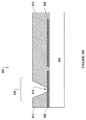
図13に示すように、連続窪み1207の幅(Wd)は、開口の幅(Wa)に対して比較的大きい。図示のように、WdはWaよりも大きい。いくつかの他の実装形態では、WdはWaのサイズの少なくとも50%である。いくつかの他の実装形態では、WdはWaの少なくとも60%、少なくとも70%、または少なくとも80%である。Waに対して比較的大きいサイズのWdは、開口を通る光が窪み1207の内面に衝突するのを促す。
As shown in FIG. 13, the width (W d ) of the
図14は、別の例示的なディスプレイ装置1400の一部分の断面図を示している。ディスプレイ装置1400は、図1400のディスプレイ装置1400と実質的に同様であるが、ディスプレイ装置1400は、MEMSアップ構成で構築される。すなわち、ディスプレイ装置1400に含まれるシャッターアセンブリ、シャッターアセンブリ1402が、図14に示すように、対向する基板上ではなく、開口プレート1404のすぐ上に形成される。シャッターアセンブリ1402は、シャッターアセンブリ1200と同様に、いくつかのシャッター開口1408を囲む横窪み部分および縦窪み部分を有する連続窪みを有するシャッター1406を含む。図14に示す断面図では、横窪み部分1410のみが見える。
FIG. 14 shows a cross-sectional view of a portion of another
図11〜図14では、シャッターアセンブリの各々に含まれる窪みは実質的に垂直の側壁を、土台にされた基板の表面に平行または垂直である表面とともに含んでいた。いくつかの他の実装形態では、他の窪みの形状が採用され得る。さらに、図示されたシャッターアセンブリの各々は、近接しているシャッター辺の任意のペアの間に、単一の窪み(または窪み部分)のみを含んでいる。いくつかの他の実装形態では、シャッターは、近接しているシャッター辺の間に複数の窪みを含み得る。いくつかの他の実装形態では、窪みは、シャッターの辺の間の距離の、上記の提案よりも小さい割合を占める。 In FIGS. 11-14, the depressions included in each of the shutter assemblies included substantially vertical sidewalls, with surfaces that were parallel or perpendicular to the surface of the substrate being mounted. In some other implementations, other recess shapes may be employed. Further, each illustrated shutter assembly includes only a single depression (or depression) between any pair of adjacent shutter edges. In some other implementations, the shutter may include multiple indentations between adjacent shutter sides. In some other implementations, the depressions occupy a smaller percentage of the distance between the sides of the shutter than the above proposal.
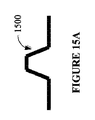
図15A〜図15Iは、シャッター窪みに適した例示的な選択的断面形状を示している。図15A〜図15Iに示す断面形状の各々は、図11に示す断面B〜B'の形状に対応する。 15A-15I illustrate exemplary selective cross-sectional shapes suitable for shutter depressions. Each of the cross-sectional shapes shown in FIGS. 15A to 15I corresponds to the shapes of cross-sections BB ′ shown in FIG.
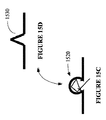
図15Aは、傾斜壁を有するシャッター窪み1500の断面図を示している。図15Bは、凹角傾斜壁を有するシャッター窪み1510の断面図を示している。図15Cは、実質的に円形の窪み1520を含む。
FIG. 15A shows a cross-sectional view of a shutter well 1500 having an inclined wall. FIG. 15B shows a cross-sectional view of a shutter well 1510 having a reclined inclined wall. FIG. 15C includes a substantially
図15Dおよび図15Eは、V字形窪み1530を示している。図15Cに示すV字形窪み1530は、シャッター辺の間の距離の実質的部分を占めていないが、いくつかの他の実装形態では、はるかに浅い角度を有するV字形窪みが形成され得る。そのような浅いV字形窪みは、そのような距離の実質的部分を占め得る。代替として、図15Eに示すように、シャッターは、2つの近接しているシャッター辺の間に複数のV字形窪み1530を含み得る。図15Eでは、全部で3つのV字形窪み1530が、シャッター辺の間の距離の実質的部分を占める。
15D and 15E show a V-shaped
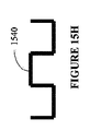
図15F〜図15Iは、選択的シャッター断面形状を示しているが、実質的に水平な表面および実質的に垂直な表面を保持し、方形窪み1540をもたらしている。図15Fは、複数の、比較的低いアスペクト比の方形窪み1540を含むシャッターの一部分を示している。図15Gは、シャッター部分の中心から外れた方形窪み1540を有するシャッターの一部分を示している。すなわち、方形窪み1540は、シャッター辺の一方に、他方よりも近い。図15Hは、シャッター部分のいずれの辺にも垂直側壁を有する、中心の方形窪み1540を有するシャッター部分を示している。図15Iは、シャッター部分のいずれの端部にも2つの方形窪み1540を有するシャッター部分を示している。実質的な平面が方形窪み1540を分離している。
FIGS. 15F-15I show selective shutter cross-sectional shapes, but retain substantially horizontal and substantially vertical surfaces, resulting in
図15A〜図15Iに示す選択的シャッター断面形状の各々は、図7A〜図7Dに関して上述した製造プロセスと同様の製造プロセスを使用して達成され得る。具体的には、いくつかの実装形態では、図示のシャッター部分を含むシャッターは、2つの層状の型に堆積された構造材料をパターニングしエッチングすることによって形成される。型の最上側面に堆積された材料は、MEMSダウン構成方位に(すなわち、図15A〜図15Iに示された方位に)配置されたときにシャッター部分の下側面としての役割を果たす。それぞれの窪みの底は、2つの型層の間の界面に堆積された材料から形成されている。型に形成される形状は、標準的なフォトパターニングおよびエッチングのプロセスを使用して形成され得る。たとえば、傾斜壁窪み1500またはV字形窪み1530の曲げられた表面は、型材料への露光の侵入を変化させるためにハーフトーンまたは高エネルギービーム感応型グラスマスクを使用して上側型層をパターニングすることによって達成され得る。凹角壁を有するシャッター窪み1510などの他の形状は、リフトオフプロセスで通常使用される凹角型材料を使用して達成され得る。
Each of the selective shutter cross-sectional shapes shown in FIGS. 15A-15I can be achieved using a manufacturing process similar to that described above with respect to FIGS. 7A-7D. Specifically, in some implementations, a shutter that includes the illustrated shutter portion is formed by patterning and etching the structural material deposited in two layered molds. The material deposited on the top side of the mold serves as the bottom side of the shutter portion when placed in the MEMS down configuration orientation (ie, in the orientation shown in FIGS. 15A-15I). The bottom of each depression is formed from a material deposited at the interface between the two mold layers. The shape formed in the mold can be formed using standard photo patterning and etching processes. For example, the curved surface of the sloped
15Hに示すシャッター部分は、バックライトから抜け出す光の直接経路の外にシャッター部分の辺があるという点で、さらなる利点をもたらす。上記で示したように、いくつかの実装形態では、本明細書で開示するシャッターは、内部金属層を含む材料の複数の層から形成される。そのようなシャッターの辺が、上側または下側の型層に実質的に平行である場合、シャッターの製造で使用される異方性エッチングプロセスおよび/またはリリースプロセスは、それらの辺における外側シャッター層の部分を除去し、下にある内部金属層を露出させることができる。 The shutter portion shown at 15H provides a further advantage in that the sides of the shutter portion are outside the direct path of light exiting the backlight. As indicated above, in some implementations, the shutters disclosed herein are formed from multiple layers of material including an internal metal layer. If the sides of such a shutter are substantially parallel to the upper or lower mold layer, the anisotropic etching process and / or release process used in the manufacture of the shutter is the outer shutter layer at those sides. Can be removed to expose the underlying internal metal layer.
露出したシャッター辺は、ディスプレイ装置の前面の方に高角度入射光を屈折させ得る。この屈折現象は図14に示されている。図14では、光1450は、ディスプレイ装置1400の前面の方に、シャッター1402の最右部分の辺で屈折する。そのような光がディスプレイから抜け出し、それによりディスプレイのコントラスト比が低下するのを防ぐために、重複Oによってシャッター1402の辺が実質的に重複するように、ディスプレイ装置1400のブラックマトリクス1460が適用される。この重複は、屈折現象から生じる光漏れを防ぐが、開口比およびディスプレイから発せられ得る角度の範囲を縮小させる。図15Hに示すように、高角度の光の経路の外にシャッター辺を位置付けることで、シャッター辺での屈折による光漏れの可能性を低減し、場合によってはなくし、それにより、ブラックマトリクスの重複の理由を除去することができる。したがって、そのようなシャッターを含むディスプレイは、ブラックマトリクスにおける開口を拡大して、視野角を拡大し、ディスプレイの輝度を上げることができる。
The exposed shutter side can refract high angle incident light towards the front of the display device. This refraction phenomenon is illustrated in FIG. In FIG. 14, the light 1450 is refracted on the rightmost side of the
図16Aは、曲げられた周囲面を有する例示的なシャッター1600の俯瞰図を示している。図16Bは、図16Aのシャッター1600の断面図を示している。断面図は、図16Aの線C〜C'で取られている。図16Aおよび図16Bを参照すると、シャッター1600は、2つのシャッター開口1604を囲む連続窪み1602を含む。シャッター1600は、2つのタイプの曲げられた周囲面、すなわち、1つの曲げられた外周囲面1606および2つ(各シャッター開口1604の周りに1つ)の曲げられたシャッター開口周囲面1608(合わせて「曲げられた周囲面1606および1608」)を含む。曲げられた周囲面1606および1608は、連続窪み1602と同じ方向で、シャッターの最上側面1610に背を向けて下に曲がっている。図16Aと図16Bの両方で、シャッター1600は、型にシャッターが形成される方法の観点から示されている。したがって、ディスプレイ装置に導入されるとき、いくつかの実装形態では、連続窪み1602がディスプレイ装置の後面の方に開き、曲げられた周囲面1606および1608がディスプレイ装置の前面の方に延びるように、シャッター1600はひっくり返される。
FIG. 16A shows an overhead view of an
いくつかの実装形態では、曲げられた周囲面1606および1608は、シャッター1600の平面の約20度〜約70度の間で曲げられる。いくつかの実装形態では、曲げられた周囲面1606および1608は、シャッターの平面の約40度〜約50度の間で曲げられる。いくつかの他の実装形態では、曲げられた周囲面1606および1608は、シャッターの平面の45度で曲げられる。総じて、選択される角度は、連続窪み1602の幅、シャッター1600が閉位置にある間に曲げられた周囲面1606および1608が開口層の対応する部分と重複する度合い、および付随するブラックマトリクスの寸法のうちの1つまたは複数の関数である。いくつかの実装形態では、外周囲面1606は、シャッター開口周囲面1608と同じ角度で曲げられる。いくつかの他の実装形態では、外周囲面1606は、シャッター開口周囲面1608とは異なる角度で曲げられる。シャッター1600のさらにいくつかの他の実装形態では、外周囲面1606のみ、またはシャッター開口周囲面1608のみが曲げられる。
In some implementations, the curved
この実装形態では、連続窪み1602の壁は、シャッター1600の平面に対して実質的に垂直または直角である。いくつかの実装形態では、連続窪み1602の壁も曲げられている。
In this implementation, the wall of the
図17は、曲げられた周囲面を有する例示的なシャッターを形成するための型1700の例示的な断面図を示している。たとえば、型1700は、図16Aおよび図16Bのシャッター1600を形成するために使用され得る。図16A、16Bおよび図17を参照すると、たとえば、2つのレベルで水平面を含む図7A〜図7Cまたは図10に関して上述した型とは異なり、型1700は3つのレベルで水平面を含む。しかしながら、型1700は、依然として型材料の2つの層のみから作られ、したがって依然として2つのパターニング段階のみを使用して十分にパターニングされ得る。下側レベル水平面1702は、下側型材料1704と上側型材料1706との間の界面1703に対応する。これらの下側レベル水平面1702上で、シャッター1600の連続窪み1602の底が形成される。中間レベル水平面1708は、シャッター開口1604およびシャッターの間の空間を形成するためにエッチングされることになるエリアに対応する。最上側水平面1710は、シャッター1600の最上側面1610が形成されるエリアに対応する。
FIG. 17 shows an exemplary cross-sectional view of a
図18は、曲げられた周囲面を有するシャッター1802を含む例示的なディスプレイ装置1800の一部分の断面図である。ディスプレイ装置1800は、シャッター1802を閉位置にしてMEMSアップ構成に従って構築される。
FIG. 18 is a cross-sectional view of a portion of an
シャッター1802は、開口プレート1850上に形成されたシャッターアセンブリ1803の一部である。ディスプレイ装置1800はまた、バックライト1852、および光をバックライト1852に取り込むための光源1854を含む。さらに、コントラストを改善するためにブラックマトリクス1855がカバープレート1810上に堆積されている。開口プレート1850は開口層1856を含み、開口層1856は開口1858を画定し、光は開口1858を通じて、シャッターアセンブリ1803によって変調されるためにディスプレイ装置1800の前面に向かってバックライト1852から抜け出すことができる。いくつかの実装形態では、開口層1856は、後ろ向き反射層および前向き光吸収層を含む。
The
ディスプレイ装置1800では、シャッター1802は連続窪み1807を含み、連続窪み1807は、窪み1807が開口層1856の方に開くように、カバープレート1810の方に突出している。この構成では、シャッター1806が閉じているとき、たいていの角度で開口層1856を通じて抜け出す光は、連続窪み1807の内面でシャッター1802に影響を与える。したがって、この光は、ディスプレイ装置1800の前面の方に戻って反射され得る前に、連続窪み1807の2つではないにせよ少なくとも1つの追加の内面に反射する可能性が高い。
In the
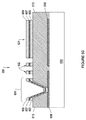
図18に示されているように、連続窪みの幅(Wd)は、開口の幅(Wa)に対して比較的大きい。図示の実装形態では、WdはWaよりも小さいが、Wdは依然として、Waのサイズの少なくとも80%である。いくつかの他の実装形態では、WdはWaのサイズの少なくとも50%である。いくつかの他の実装形態では、WdはWaの少なくとも60%、または少なくとも70%である。さらに他の実装形態では、WdはWaよりも大きい。Waに対して比較的大きいサイズのWdは、開口を通る光が窪み1807の内面に衝突するのを促す。
As shown in FIG. 18, the width of the continuous depression (W d ) is relatively large with respect to the width of the opening (W a ). In the illustrated implementation, W d is smaller than W a , but W d is still at least 80% of the size of W a . In some other implementations, W d is at least 50% of the size of W a . In some other implementations, W d is at least 60%, or at least 70% of W a . In still other implementations, W d is greater than W a . W d having a relatively large size with respect to W a urges light passing through the opening to collide with the inner surface of the
図14のディスプレイ装置1400とは対照的に、ディスプレイ1800のシャッターアセンブリ1803は、曲げられた周囲面1812を有するシャッター1802を含む。したがって、シャッター1802の辺は、図14のディスプレイ装置におけるシャッター1307の辺で屈折した高角度の光の経路の外にある。その結果、ディスプレイ装置1800は、ブラックマトリクス1855とシャッター1802の辺との間の重複を解消する。代わりに、いくつかの実装形態では、ブラックマトリクス1855の辺は、シャッター1802の辺と実質的に整合する。
In contrast to the
図19は、曲げられた周囲面を有するシャッター1902を含む別の例示的なディスプレイ装置1900の一部分の断面図を示している。ディスプレイ装置1900は、シャッター1902を閉位置にしてMEMSアップ構成に従って構築されている。図18のディスプレイ装置1800のシャッター1802とは対照的に、シャッター1902は2つの連続窪み1904を含む。さらに、各窪み1904の1つの壁は、窪みがちょうどシャッター1902の辺にちょうど一致して延びているので、曲げられた周囲面としての役割を果たしている。その上、シャッター1902の曲げられた表面は、ディスプレイ装置1900の前面の方ではなく後面の方に延びている。窪みは、シャッターの辺に一致して配置されており、光を捕捉するのに非常に効果的である。その上、曲げられた周囲面を形成するようにシャッター1902の辺を曲げることによって、光がディスプレイ装置1900の前面の方に屈折する可能性がより小さくなる。
FIG. 19 shows a cross-sectional view of a portion of another exemplary display device 1900 that includes a shutter 1902 having a curved peripheral surface. Display device 1900 is constructed according to the MEMS up configuration with shutter 1902 in the closed position. In contrast to the
図20は、曲げられた周囲面を有するシャッター2002を含む別の例示的なディスプレイ装置2000の一部分の断面図を示している。ディスプレイ装置2000は、シャッター2002を閉位置にしてMEMSアップ構成に従って構築されている。図19のディスプレイ装置1900のシャッター1902とは対照的に、シャッター2002は、シャッターの外壁を形成し、シャッター開口を囲む曲げられた周囲面2006によって境界が示されたただ1つのより大きい連続窪み2004のみを含む。図19のシャッター1902と同様に、シャッター2002の曲げられた表面2006は、ディスプレイ装置2000の前面の方ではなく後面の方に延びている。窪み2004は、シャッターの辺に一致して延びており、光を捕捉するのに非常に効果的である。その上、曲げられた周囲面2006を形成するようにシャッター2002の辺を曲げることによって、光がディスプレイ装置2000の前面の方に屈折する可能性がより小さくなる。
FIG. 20 illustrates a cross-sectional view of a portion of another
本明細書で開示した実装形態に関連して説明した様々な例示的な論理、論理ブロック、モジュール、回路およびアルゴリズムのプロセスは、電子ハードウェア、コンピュータソフトウェア、または両方の組合せとして実装され得る。ハードウェアとソフトウェアの互換性は、全体的にそれらの機能に関して説明し、上述の様々な例示的な構成要素、ブロック、モジュール、回路およびプロセスにおいて示してきた。そのような機能がハードウェアとして実装されるか、またはソフトウェアとして実装されるかは、特定の適用例および全体的なシステムに課された設計制約に依存する。 The various exemplary logic, logic blocks, modules, circuits, and algorithmic processes described in connection with the implementations disclosed herein may be implemented as electronic hardware, computer software, or a combination of both. Hardware and software compatibility has been described generally in terms of their functionality and has been demonstrated in the various exemplary components, blocks, modules, circuits and processes described above. Whether such functionality is implemented as hardware or software depends upon the particular application and design constraints imposed on the overall system.
本明細書で開示した態様に関連して説明した様々な例示的な論理、論理ブロック、モジュールおよび回路を実装するために使用されるハードウェアおよびデータ処理装置は、汎用シングルチッププロセッサもしくは汎用マルチチッププロセッサ、デジタル信号プロセッサ(DSP)、特定用途向け集積回路(ASIC)、フィールドプログラマブルゲートアレイ(FPGA)もしくは他のプログラマブル論理デバイス、個別ゲートもしくはトランジスタ論理、個別ハードウェア構成要素、または、本明細書で説明した機能を実行するように設計されたそれらの任意の組合せで、実装または実行することができる。汎用プロセッサはマイクロプロセッサ、または任意の従来のプロセッサ、コントローラ、マイクロコントローラ、もしくは状態機械であり得る。プロセッサはまた、コンピューティングデバイスの組合せ、たとえば、DSPとマイクロプロセッサとの組合せ、複数のマイクロプロセッサ、DSPコアと連携する1つもしくは複数のマイクロプロセッサ、または任意の他のそのような構成として実装され得る。いくつかの実装形態では、特定のプロセスおよび方法は、所与の機能に固有の回路によって実行され得る。 The hardware and data processing apparatus used to implement the various exemplary logic, logic blocks, modules and circuits described in connection with the aspects disclosed herein may be a general purpose single chip processor or a general purpose multichip. Processor, digital signal processor (DSP), application specific integrated circuit (ASIC), field programmable gate array (FPGA) or other programmable logic device, individual gate or transistor logic, individual hardware components, or as used herein It can be implemented or performed in any combination thereof designed to perform the functions described. A general purpose processor may be a microprocessor, or any conventional processor, controller, microcontroller, or state machine. The processor is also implemented as a combination of computing devices, eg, a DSP and microprocessor combination, a plurality of microprocessors, one or more microprocessors associated with a DSP core, or any other such configuration. obtain. In some implementations, certain processes and methods may be performed by circuitry that is specific to a given function.
1つまたは複数の態様では、説明した機能は、本明細書で開示した構造およびそれらの構造の同等物を含む、ハードウェア、デジタル電子回路、コンピュータソフトウェア、ファームウェアにおいて、またはそれらの任意の組合せで実装され得る。本明細書で説明した対象の実装形態はまた、1つまたは複数のコンピュータプログラム、すなわち、データ処理装置による実行のために、またはデータ処理装置の動作を制御するために、コンピュータ記憶媒体上に符号化されたコンピュータプログラム命令の1つまたは複数のモジュールとして実装され得る。 In one or more aspects, the functions described can be in hardware, digital electronic circuitry, computer software, firmware, or any combination thereof, including the structures disclosed herein and their equivalents. Can be implemented. The subject implementations described herein may also be encoded on a computer storage medium for execution by one or more computer programs, ie, data processing devices, or for controlling the operation of data processing devices. May be implemented as one or more modules of computerized computer program instructions.
本開示で説明した実装形態の様々な修正形態が当業者にはすぐに理解でき、本明細書に定める一般的原理は、本開示の趣旨または範囲から離れることなく他の実装形態に適用できる。したがって、特許請求の範囲は、本明細書に示す実装形態に限定されることを意図しておらず、本開示、この原理および本明細書で開示する新規の特徴体と合致する最大の範囲を認めるものである。 Various modifications to the implementations described in this disclosure will be readily apparent to those skilled in the art, and the general principles defined herein may be applied to other implementations without departing from the spirit or scope of this disclosure. Accordingly, the claims are not intended to be limited to the implementations shown herein, but to the greatest extent consistent with this disclosure, this principle, and the novel features disclosed herein. It is what you admit.
さらに、当業者は、「上側」および「下側」という用語が、図の説明を簡単にするために使用されることがあり、適切に配向されたページ上の図の方位に対応する相対位置を示しており、実装される任意のデバイスの適切な方位を反映していない場合があることを容易に諒解する。 Moreover, those skilled in the art will recognize that the terms “upper” and “lower” may be used to simplify the illustration of the figure, relative positions corresponding to the orientation of the figure on a properly oriented page. And easily understand that it may not reflect the proper orientation of any device being implemented.
個別の実装形態との関連で本明細書で説明しているいくつかの特徴体は、単一の実装形態において組合せで実装されてもよい。反対に、単一の実装形態との関連で説明している様々な特徴体は、複数の実装形態で個別に、または任意の適切な副組合せで実装されてもよい。さらに、特徴体は一定の組合せで機能するものとして上述され、当初はそういうものとして特許請求されることもあるが、特許請求される組合せによる1つまたは複数の特徴体は、場合によっては、当該組合せにより実施可能であり、特許請求される組合せは、副組合せまたは副組合せの変形を対象にし得る。 Some features described herein in the context of separate implementations may be implemented in combination in a single implementation. Conversely, the various features described in the context of a single implementation may be implemented individually in multiple implementations or in any suitable subcombination. Further, while a feature is described above as functioning in a certain combination and may initially be claimed as such, one or more features in the claimed combination may, in some cases, Combinations can be implemented and claimed combinations may be directed to subcombinations or variations of subcombinations.
同様に、動作は特定の順序で図面に示されているが、これについては、所望の結果を達成するために、そのような動作を示された特定の順序でもしくは順次に実行すること、またはすべての示された動作を実行することを要求するものとして理解すべきではない。さらに、図面は、1つまたは複数の例示的なプロセスをフロー図の形式で概略的に示し得る。しかしながら、図示されていない他の動作を、概略的に示す例示的なプロセスに組み込むことができる。たとえば、1つまたは複数の追加の動作は、示された動作のいずれかの前、示された動作のいずれかの後、示された動作のいずれかと同時に、または示された動作のいずれかの間に実行され得る。いくつかの状況において、マルチタスキングおよび並列処理は有利であり得る。また、上述の実装形態における様々なシステム構成要素の分離については、すべての実装形態でかかる分離を要求するものとして理解すべきではなく、説明されるプログラム構成要素およびシステムは一般に単一のソフトウェア製品への統合、または複数のソフトウェア製品へのパッケージ化が可能であると理解されたい。さらに、他の実装形態も、以下の特許請求の範囲内に入る。場合によっては、請求項に記載の動作は、異なる順序で実行されながらもなお、望ましい結果を達成することが可能である。 Similarly, operations are shown in the drawings in a particular order, which may be performed in the particular order shown or sequentially in order to achieve the desired result, or It should not be understood as requiring that all the indicated operations be performed. Further, the drawings may schematically illustrate one or more exemplary processes in the form of a flow diagram. However, other operations not shown can be incorporated into the exemplary process shown schematically. For example, the one or more additional actions may occur before any of the indicated actions, after any of the indicated actions, simultaneously with any of the indicated actions, or any of the indicated actions. Can be performed in between. In some situations, multitasking and parallel processing may be advantageous. Also, the separation of various system components in the implementations described above should not be understood as requiring such separation in all implementations, and the program components and systems described are generally a single software product. It should be understood that it can be integrated into or packaged into multiple software products. Furthermore, other implementations are within the scope of the following claims. In some cases, the actions recited in the claims can be performed in a different order and still achieve desirable results.
100 ディスプレイ装置
102 光変調器
102a 光変調器
102b 光変調器
102c 光変調器
102d 光変調器
104 画像
105 ランプ
106 画素
108 シャッター
109 開口
110 書込み許可相互接続
112 データ相互接続
114 共通相互接続
120 ブロック図
122 ホストプロセッサ
124 環境センサ
126 ユーザ入力モジュール
128 ディスプレイ装置
130 スキャンドライバ
132 データドライバ
134 コントローラ
138 共通ドライバ
140 ランプ
142 ランプ
144 ランプ
146 ランプ
148 ランプドライバ
200 シャッターアセンブリ
202 シャッター
203 表面
204 アクチュエータ
205 コンプライアント電極ビームアクチュエータ
206 コンプライアントロードビーム
207 スプリング
208 ロードアンカ
211 開口穴
216 コンプライアント駆動ビーム
218 駆動ビームアンカ
300 制御マトリクス
301 画素
302 シャッターアセンブリ
303 アクチュエータ
304 基板
306 スキャンライン相互接続
307 書込み許可電圧源
308 データ相互接続
309 データ電圧源
310 トランジスタ
312 キャパシタ
320 光変調器アレイ
322 開口層
324 開口
400 二重アクチュエータシャッターアセンブリ
402 シャッター開アクチュエータ
404 シャッター閉アクチュエータ
406 シャッター
407 開口層
408 アンカ
409 開口
412 シャッター開口
416 重複
500 ディスプレイ装置
502 シャッターアセンブリ
503 シャッター
504 基板
505 アンカ
506 反射開口層
508 表面開口
512 ディフューザ
514 輝度増強膜
515 バックライト
516 光ガイド
517 光リダイレクタ
518 光源
519 反射体
520 前向き反射膜
521 光線
522 カバープレート
524 ブラックマトリクス
526 ギャップ
527 スペーサ
528 粘着シール
530 流体
532 アセンブリブラケット
536 反射体
600 シャッターアセンブリ
601 シャッター
602 コンプライアントビーム
603 基板
604 アンカ
605 第1の機械層
606 開口層
607 導体層、導電層
609 第2の機械層
611 封入誘電体
613 犠牲層
614 導電面
700 シャッターアセンブリ
701 第1の犠牲材料
702 開口またはビア
703 型
705 第2の犠牲材料
708 下水平レベル、下水平面
709 側壁
710 上水平レベル、上水平面
712 シャッター
714 アンカ
716 コンプライアントスプリングビーム
718 コンプライアントアクチュエータビーム
720 コンプライアントアクチュエータビーム
724 分離ポイント
725 開口層
852 シャッターアセンブリ
854 二重コンプライアントアクチュエータアセンブリ
856 コンプライアント駆動ビーム
857 コンプライアント駆動ビーム
858 コンプライアントロードビーム
859 コンプライアントロードビーム
860 シャッター
862 ロードビームアンカ
863 ロードビームアンカ
864 共通アンカ
900 シャッターアセンブリ
902 シャッター
903 リブへこみ
904 ロードビーム
905 シャッター開口
906 ロードビームアンカ
908 駆動ビーム
909 垂直壁
910 駆動ビームアンカ
912 周辺ビーム
914 周辺ビームアンカ
1000 型
1003 リブへこみ
1004 凹部
1006 ロードビームアンカ穴
1008 メサ形状
1010 駆動ビームアンカ穴
1100 シャッターアセンブリ
1102 シャッター
1104 静電アクチュエータ
1106 アンカ
1108 基板
1110 横窪み
1112 縦窪み
1114 シャッター開口
1115 平面
1200 シャッターアセンブリ
1202 シャッター
1204 静電アクチュエータ
1206 アンカ
1207 連続窪み
1208 基板
1210 基板
1212 シャッター開口
1300 ディスプレイ装置
1350 開口プレート
1352 バックライト
1354 光源
1356 開口層
1358 開口
1400 ディスプレイ装置
1402 シャッターアセンブリ
1404 開口プレート
1406 シャッター
1408 シャッター開口
1410 横窪み部分
1450 光
1460 ブラックマトリクス
1500 シャッター窪み
1510 シャッター窪み
1520 円形の窪み
1530 V字形窪み
1540 方形窪み
1600 シャッター
1602 連続窪み
1604 シャッター開口
1606 外周囲面
1608 シャッター開口周囲面
1610 最上側面
1700 型
1702 下側レベル水平面
1703 界面
1704 下側型材料
1706 上側型材料
1708 中間レベル水平面
1710 最上側水平面
1800 ディスプレイ装置
1802 シャッター
1803 シャッターアセンブリ
1807 連続窪み
1810 カバープレート
1812 曲げられた周囲面
1850 開口プレート
1852 バックライト
1854 光源
1855 ブラックマトリクス
1856 開口層
1858 開口
1900 ディスプレイ装置
1902 シャッター
1904 連続窪み
2000 ディスプレイ装置
2002 シャッター
2004 連続窪み
2006 曲げられた周囲面
DESCRIPTION OF SYMBOLS 100 Display apparatus 102 Optical modulator 102a Optical modulator 102b Optical modulator 102c Optical modulator 102d Optical modulator 104 Image 105 Lamp 106 Pixel 108 Shutter 109 Aperture 110 Write permission interconnection 112 Data interconnection 114 Common interconnection 120 Block diagram 122 Host processor 124 Environmental sensor 126 User input module 128 Display device 130 Scan driver 132 Data driver 134 Controller 138 Common driver 140 Lamp 142 Lamp 144 Lamp 146 Lamp 148 Lamp driver 200 Shutter assembly 202 Shutter 203 Surface 204 Actuator 205 Compliant electrode beam actuator 206 Compliant load beam 07 Spring 208 Load anchor 211 Open hole 216 Compliant drive beam 218 Drive beam anchor 300 Control matrix 301 Pixel 302 Shutter assembly 303 Actuator 304 Substrate 306 Scan line interconnect 307 Write enable voltage source 308 Data interconnect 309 Data voltage source 310 Transistor 312 Capacitor 320 Light modulator array 322 Aperture layer 324 Aperture 400 Double actuator shutter assembly 402 Shutter open actuator 404 Shutter close actuator 406 Shutter 407 Aperture layer 408 Anchor 409 Aperture 412 Shutter aperture 416 Overlap 500 Display device 502 Shutter assembly 503 Shutter 504 Substrate 505 Anka 506 Reflective aperture layer 508 Surface aperture 512 Diffuser 514 Brightness enhancement film 515 Backlight 516 Light guide 517 Light redirector 518 Light source 519 Reflector 520 Forward reflective film 521 Light beam 522 Cover plate 524 Black matrix 526 Gap 527 Spacer 528 Adhesive seal 532 Bracket 536 Reflector 600 Shutter assembly 601 Shutter 602 Compliant beam 603 Substrate 604 Anchor 605 First mechanical layer 606 Opening layer 607 Conductive layer, conductive layer 609 Second mechanical layer 611 Encapsulating dielectric 613 Sacrificial layer 614 Conductive surface 700 Shutter Assembly 701 first sacrificial material 702 opening or via 703 mold 705 second sacrificial material 708 lower horizontal level, lower Horizontal plane 709 Side wall 710 Upper horizontal level, upper horizontal plane 712 Shutter 714 Anchor 716 Compliant spring beam 718 Compliant actuator beam 720 Compliant actuator beam 724 Separation point 725 Aperture layer 852 Shutter assembly 854 Dual compliant actuator assembly 856 Compliant drive beam 857 Compliant drive beam 858 Compliant load beam 859 Compliant load beam 860 Shutter 862 Load beam anchor 863 Load beam anchor 864 Common anchor 900 Shutter assembly 902 Shutter 903 Rib dent 904 Load beam 905 Shutter opening 906 Load beam anchor 08 Drive beam 909 Vertical wall 910 Drive beam anchor 912 Peripheral beam 914 Peripheral beam anchor 1000 type 1003 Rib dent 1004 Recess 1006 Load beam anchor hole 1008 Mesa shape 1010 Drive beam anchor hole 1100 Shutter assembly 1102 Shutter 1104 Electrostatic actuator 1106 Anchor 1108 Substrate 1110 Horizontal depression 1112 Vertical depression 1114 Shutter opening 1115 Plane 1200 Shutter assembly 1202 Shutter 1204 Electrostatic actuator 1206 Anchor 1207 Continuous depression 1208 Substrate 1210 Substrate 1212 Shutter opening 1300 Display device 1350 Opening plate 1352 Back light 1354 Opening layer 1354 Opening layer 1354 Opening layer Playing device 1402 Shutter assembly 1404 Opening plate 1406 Shutter 1408 Shutter opening 1410 Horizontal recess 1450 Light 1460 Black matrix 1500 Shutter recess 1510 Shutter recess 1520 Circular recess 1530 V-shaped recess 1540 Square recess 1600 Outer shutter 1604 Peripheral recess 1604 Surface 1608 Shutter opening peripheral surface 1610 Top side 1700 type 1702 Lower level horizontal surface 1703 Interface 1704 Lower side material 1706 Upper side material 1708 Middle level horizontal surface 1710 Upper side horizontal surface 1800 Display device 1802 Shutter 1803 Shutter assembly 1807 Continuous recess 1810 Cover plate 1812 Bent perimeter 1 850 Aperture plate 1852 Backlight 1854 Light source 1855 Black matrix 1856 Aperture layer 1858 Aperture 1900 Display device 1902 Shutter 1904 Continuous depression 2000 Display device 2002 Shutter 2004 Continuous depression 2006 Curved peripheral surface
Claims (13)
バックライトと、
複数の開口を画定する、前記バックライトの前面に配置された開口層と、
前記ディスプレイ装置上に画像を形成するために、前記開口を通る前記バックライトによって発せられた光を変調するように構成されたマイクロ電気機械システム(MEMS)光変調器と
を含み、前記MEMS光変調器はシャッターを含み、前記シャッターは、
開口層向き表面および前向き表面を有する遮光部分と、
前記遮光部分に形成された少なくとも1つの窪みと
を有し、前記少なくとも1つの窪みの幅は、前記シャッターの2つの辺を分離する距離の50%以上を占め、
前記遮光部分は、前記遮光部分に形成された前記少なくとも1つの窪みの側壁から離れる方向であって、前記遮光部分に確定されたシャッター開口に向かう方向に延設する最上面を含み、前記最上面は、前記シャッター開口と前記少なくとも1つの窪みの側壁との間に配置され、
前記最上面は、前記側壁の、前記少なくとも1つの窪みの底部とは反対方向の端部に配置され、
前記遮光部分に形成された前記少なくとも1つの窪みの面積は、前記開口層における対応する開口の面積よりも広い、ディスプレイ装置。 A display device,
With backlight,
An aperture layer disposed in front of the backlight that defines a plurality of apertures;
A microelectromechanical system (MEMS) light modulator configured to modulate light emitted by the backlight through the opening to form an image on the display device, the MEMS light modulation The vessel includes a shutter, the shutter
A light shielding portion having an opening layer facing surface and a forward facing surface;
Having at least one recess formed in the light shielding portion, and the width of the at least one recess occupies 50% or more of the distance separating the two sides of the shutter;
The light shielding portion includes an uppermost surface extending in a direction away from a side wall of the at least one depression formed in the light shielding portion and toward a shutter opening defined in the light shielding portion, and the uppermost surface Is disposed between the shutter opening and the side wall of the at least one depression,
The top surface is disposed at an end of the side wall opposite to a bottom of the at least one depression ;
The display device , wherein an area of the at least one depression formed in the light shielding portion is larger than an area of a corresponding opening in the opening layer .
前記シャッターの前記2つの辺は、前記シャッターの外周囲辺および前記シャッター開口の辺を含む、請求項1に記載のディスプレイ装置。 The shutter opening is configured to allow light to pass through the shutter in an open position;
The display device according to claim 1, wherein the two sides of the shutter include an outer peripheral side of the shutter and a side of the shutter opening.
前記シャッターは、前記窪みの長さが前記シャッター開口の長さに対して直角になるように前記シャッター開口と前記シャッターの側面との間に配置された側面窪みをさらに含む、請求項1に記載のディスプレイ装置。 The shutter opening is configured to allow light to pass through the shutter in an open position;
2. The shutter according to claim 1, further comprising a side recess disposed between the shutter opening and a side surface of the shutter such that a length of the recess is perpendicular to a length of the shutter opening. Display device.
前記プロセッサと通信するように構成されたメモリデバイスと
を含む、請求項1に記載のディスプレイ装置。 A processor configured to process image data;
The display device of claim 1, comprising a memory device configured to communicate with the processor.
をさらに含み、
前記プロセッサは、前記ドライバ回路に前記画像データの少なくとも一部分を送るようにさらに構成される、請求項11に記載のディスプレイ装置。 A driver circuit configured to send at least one signal to one of the MEMS light modulator and the backlight;
The display device of claim 11 , wherein the processor is further configured to send at least a portion of the image data to the driver circuit.
をさらに含む、請求項11に記載のディスプレイ装置。 The display apparatus of claim 11 , further comprising an input device configured to receive input data and communicate the input data to the processor.
Applications Claiming Priority (3)
| Application Number | Priority Date | Filing Date | Title |
|---|---|---|---|
| US13/486,722 | 2012-06-01 | ||
| US13/486,722 US9063333B2 (en) | 2012-06-01 | 2012-06-01 | Microelectromechanical device and method of manufacturing |
| PCT/US2013/039652 WO2013180903A1 (en) | 2012-06-01 | 2013-05-06 | Display apparatus comprising micro-electromechanical light modulator including a shutter |
Publications (3)
| Publication Number | Publication Date |
|---|---|
| JP2015519607A JP2015519607A (en) | 2015-07-09 |
| JP2015519607A5 JP2015519607A5 (en) | 2016-06-02 |
| JP6246798B2 true JP6246798B2 (en) | 2017-12-13 |
Family
ID=48534483
Family Applications (1)
| Application Number | Title | Priority Date | Filing Date |
|---|---|---|---|
| JP2015515016A Active JP6246798B2 (en) | 2012-06-01 | 2013-05-06 | Microelectromechanical device and manufacturing method |
Country Status (7)
| Country | Link |
|---|---|
| US (1) | US9063333B2 (en) |
| EP (1) | EP2856238A1 (en) |
| JP (1) | JP6246798B2 (en) |
| KR (1) | KR20150015539A (en) |
| CN (1) | CN104350410B (en) |
| TW (1) | TWI566223B (en) |
| WO (1) | WO2013180903A1 (en) |
Families Citing this family (10)
| Publication number | Priority date | Publication date | Assignee | Title |
|---|---|---|---|---|
| US20140225904A1 (en) * | 2013-02-13 | 2014-08-14 | Pixtronix, Inc. | Shutter assemblies fabricated on multi-height molds |
| US20150279282A1 (en) * | 2014-03-28 | 2015-10-01 | Pixtronix, Inc. | Distributed electrostatic actuator for mems devices |
| CN105700226A (en) * | 2016-04-25 | 2016-06-22 | 京东方科技集团股份有限公司 | Viewing angle control mechanism, light guide plate, backlight module, array substrate and display panel |
| CN105700243A (en) * | 2016-04-29 | 2016-06-22 | 京东方科技集团股份有限公司 | Display panel and display device thereof |
| CN105895023B (en) * | 2016-06-03 | 2019-03-15 | 深圳市华星光电技术有限公司 | Micro electronmechanical light valve, display screen and display device |
| CN107577043B (en) * | 2016-07-04 | 2021-10-08 | 爱德华·帕克奇亚恩 | MEMS light modulator for display |
| JP6953116B2 (en) * | 2016-07-04 | 2021-10-27 | エドワード・パクチャン | MEMS display |
| JP7015104B2 (en) * | 2016-07-04 | 2022-02-15 | エドワード・パクチャン | MEMS display |
| KR102590788B1 (en) * | 2016-07-04 | 2023-10-17 | 에드워드 파크얀 | Mems display |
| CN115567777B (en) * | 2022-09-30 | 2023-08-29 | 杭州海康微影传感科技有限公司 | Micro-electromechanical baffle and preparation method thereof, image sensor assembly and preparation method thereof, image sensor and manufacturing method thereof |
Family Cites Families (13)
| Publication number | Priority date | Publication date | Assignee | Title |
|---|---|---|---|---|
| CN1190687C (en) * | 2002-02-07 | 2005-02-23 | 台湾积体电路制造股份有限公司 | Refective liquid crystal light gate with obstruction member |
| US7417782B2 (en) * | 2005-02-23 | 2008-08-26 | Pixtronix, Incorporated | Methods and apparatus for spatial light modulation |
| CN100470305C (en) * | 2004-09-27 | 2009-03-18 | Idc公司 | System and method for protecting microelectromechanical systems array using structurally reinforced back-plate |
| CN1755495A (en) * | 2004-09-27 | 2006-04-05 | Idc公司 | Method of making prestructure for MEMS systems |
| US7405852B2 (en) * | 2005-02-23 | 2008-07-29 | Pixtronix, Inc. | Display apparatus and methods for manufacture thereof |
| ATE414971T1 (en) * | 2005-02-23 | 2008-12-15 | Pixtronix Inc | LIGHT MODULATOR AND METHOD FOR THE PRODUCTION THEREOF |
| US8526096B2 (en) * | 2006-02-23 | 2013-09-03 | Pixtronix, Inc. | Mechanical light modulators with stressed beams |
| WO2008091339A2 (en) | 2007-01-19 | 2008-07-31 | Pixtronix, Inc. | Mems display apparatus |
| CN201066421Y (en) * | 2007-07-05 | 2008-05-28 | 比亚迪股份有限公司 | Back light module and LCD capable of preventing light leakage |
| US8169679B2 (en) | 2008-10-27 | 2012-05-01 | Pixtronix, Inc. | MEMS anchors |
| KR20120129256A (en) * | 2011-05-19 | 2012-11-28 | 삼성디스플레이 주식회사 | Display substrate, method of manufacturing the same and display panel having the display substrate |
| JP5856759B2 (en) * | 2011-06-03 | 2016-02-10 | ピクストロニクス,インコーポレイテッド | Display device |
| US9809445B2 (en) | 2011-08-26 | 2017-11-07 | Qualcomm Incorporated | Electromechanical system structures with ribs having gaps |
-
2012
- 2012-06-01 US US13/486,722 patent/US9063333B2/en not_active Expired - Fee Related
-
2013
- 2013-05-06 CN CN201380029042.1A patent/CN104350410B/en not_active Expired - Fee Related
- 2013-05-06 KR KR1020147037040A patent/KR20150015539A/en not_active Application Discontinuation
- 2013-05-06 EP EP13725508.9A patent/EP2856238A1/en not_active Withdrawn
- 2013-05-06 WO PCT/US2013/039652 patent/WO2013180903A1/en active Application Filing
- 2013-05-06 JP JP2015515016A patent/JP6246798B2/en active Active
- 2013-05-14 TW TW102117067A patent/TWI566223B/en not_active IP Right Cessation
Also Published As
| Publication number | Publication date |
|---|---|
| KR20150015539A (en) | 2015-02-10 |
| EP2856238A1 (en) | 2015-04-08 |
| JP2015519607A (en) | 2015-07-09 |
| TW201401253A (en) | 2014-01-01 |
| CN104350410B (en) | 2018-02-06 |
| US9063333B2 (en) | 2015-06-23 |
| US20130322058A1 (en) | 2013-12-05 |
| WO2013180903A1 (en) | 2013-12-05 |
| CN104350410A (en) | 2015-02-11 |
| TWI566223B (en) | 2017-01-11 |
Similar Documents
| Publication | Publication Date | Title |
|---|---|---|
| JP6246798B2 (en) | Microelectromechanical device and manufacturing method | |
| JP5788601B2 (en) | Electromechanical system structure with ribs having gaps | |
| JP5689803B2 (en) | Manufacturing structure and process for compliant mechanisms | |
| JP6090888B2 (en) | Display device with narrow gap electrostatic actuator | |
| US9201236B2 (en) | Display apparatus with stiction reduction features | |
| JP2016513823A (en) | Display device incorporating dual level shutter | |
| JP6051422B2 (en) | MEMS anchor and spacer structure | |
| TW201314312A (en) | Displays having self-aligned apertures and methods of making the same | |
| JP2015535347A (en) | Display device incorporating vertically oriented electrical interconnects | |
| JP2016503191A (en) | Display device incorporating multiple dielectric layers | |
| TWI504929B (en) | Display apparatus incorporating multi-level shutters and method for forming a multi-level display device | |
| JP6216032B2 (en) | MEMS shutter assembly for high resolution displays | |
| TWI516799B (en) | An apparatus having an electrostatic actuation assembly for controlling the position of a suspeneded portion of a display element and a method for forming an electrostatic actuator | |
| CN103777344B (en) | Manufacture structures and methods for pliable mechanism |
Legal Events
| Date | Code | Title | Description |
|---|---|---|---|
| A521 | Request for written amendment filed |
Free format text: JAPANESE INTERMEDIATE CODE: A523 Effective date: 20160406 |
|
| A621 | Written request for application examination |
Free format text: JAPANESE INTERMEDIATE CODE: A621 Effective date: 20160406 |
|
| A711 | Notification of change in applicant |
Free format text: JAPANESE INTERMEDIATE CODE: A711 Effective date: 20161116 |
|
| A977 | Report on retrieval |
Free format text: JAPANESE INTERMEDIATE CODE: A971007 Effective date: 20170131 |
|
| A131 | Notification of reasons for refusal |
Free format text: JAPANESE INTERMEDIATE CODE: A131 Effective date: 20170206 |
|
| A521 | Request for written amendment filed |
Free format text: JAPANESE INTERMEDIATE CODE: A523 Effective date: 20170502 |
|
| TRDD | Decision of grant or rejection written | ||
| A01 | Written decision to grant a patent or to grant a registration (utility model) |
Free format text: JAPANESE INTERMEDIATE CODE: A01 Effective date: 20171023 |
|
| A61 | First payment of annual fees (during grant procedure) |
Free format text: JAPANESE INTERMEDIATE CODE: A61 Effective date: 20171115 |
|
| R150 | Certificate of patent or registration of utility model |
Ref document number: 6246798 Country of ref document: JP Free format text: JAPANESE INTERMEDIATE CODE: R150 |
|
| R250 | Receipt of annual fees |
Free format text: JAPANESE INTERMEDIATE CODE: R250 |
|
| R250 | Receipt of annual fees |
Free format text: JAPANESE INTERMEDIATE CODE: R250 |
|
| R250 | Receipt of annual fees |
Free format text: JAPANESE INTERMEDIATE CODE: R250 |