KR20130126948A - Semiconductor devices with back surface isolation - Google Patents
Semiconductor devices with back surface isolation Download PDFInfo
- Publication number
- KR20130126948A KR20130126948A KR1020137017405A KR20137017405A KR20130126948A KR 20130126948 A KR20130126948 A KR 20130126948A KR 1020137017405 A KR1020137017405 A KR 1020137017405A KR 20137017405 A KR20137017405 A KR 20137017405A KR 20130126948 A KR20130126948 A KR 20130126948A
- Authority
- KR
- South Korea
- Prior art keywords
- conductive
- substrate
- layer
- well
- region
- Prior art date
Links
- 239000004065 semiconductor Substances 0.000 title claims abstract description 120
- 238000002955 isolation Methods 0.000 title claims description 90
- 239000000463 material Substances 0.000 claims abstract description 134
- 238000000034 method Methods 0.000 claims abstract description 78
- 239000000758 substrate Substances 0.000 claims description 180
- JMASRVWKEDWRBT-UHFFFAOYSA-N Gallium nitride Chemical compound [Ga]#N JMASRVWKEDWRBT-UHFFFAOYSA-N 0.000 claims description 91
- 229910052710 silicon Inorganic materials 0.000 claims description 57
- 239000010703 silicon Substances 0.000 claims description 56
- XUIMIQQOPSSXEZ-UHFFFAOYSA-N Silicon Chemical compound [Si] XUIMIQQOPSSXEZ-UHFFFAOYSA-N 0.000 claims description 55
- 229910002601 GaN Inorganic materials 0.000 claims description 52
- 229910052782 aluminium Inorganic materials 0.000 claims description 30
- XAGFODPZIPBFFR-UHFFFAOYSA-N aluminium Chemical compound [Al] XAGFODPZIPBFFR-UHFFFAOYSA-N 0.000 claims description 30
- 230000004888 barrier function Effects 0.000 claims description 27
- 238000005468 ion implantation Methods 0.000 claims description 26
- RNQKDQAVIXDKAG-UHFFFAOYSA-N aluminum gallium Chemical compound [Al].[Ga] RNQKDQAVIXDKAG-UHFFFAOYSA-N 0.000 claims description 24
- 238000004519 manufacturing process Methods 0.000 claims description 16
- NRTOMJZYCJJWKI-UHFFFAOYSA-N Titanium nitride Chemical compound [Ti]#N NRTOMJZYCJJWKI-UHFFFAOYSA-N 0.000 claims description 14
- 229920002120 photoresistant polymer Polymers 0.000 claims description 13
- 239000010931 gold Substances 0.000 claims description 11
- 239000012535 impurity Substances 0.000 claims description 10
- 238000000151 deposition Methods 0.000 claims description 9
- 150000002500 ions Chemical class 0.000 claims description 9
- ZOXJGFHDIHLPTG-UHFFFAOYSA-N Boron Chemical compound [B] ZOXJGFHDIHLPTG-UHFFFAOYSA-N 0.000 claims description 8
- 229910052796 boron Inorganic materials 0.000 claims description 8
- 239000003989 dielectric material Substances 0.000 claims description 8
- 239000012212 insulator Substances 0.000 claims description 8
- HBMJWWWQQXIZIP-UHFFFAOYSA-N silicon carbide Chemical compound [Si+]#[C-] HBMJWWWQQXIZIP-UHFFFAOYSA-N 0.000 claims description 7
- WFKWXMTUELFFGS-UHFFFAOYSA-N tungsten Chemical compound [W] WFKWXMTUELFFGS-UHFFFAOYSA-N 0.000 claims description 7
- 229910052721 tungsten Inorganic materials 0.000 claims description 7
- 239000010937 tungsten Substances 0.000 claims description 7
- 239000010949 copper Substances 0.000 claims description 6
- PCHJSUWPFVWCPO-UHFFFAOYSA-N gold Chemical compound [Au] PCHJSUWPFVWCPO-UHFFFAOYSA-N 0.000 claims description 6
- 229910052737 gold Inorganic materials 0.000 claims description 6
- 239000004020 conductor Substances 0.000 claims description 5
- JBRZTFJDHDCESZ-UHFFFAOYSA-N AsGa Chemical compound [As]#[Ga] JBRZTFJDHDCESZ-UHFFFAOYSA-N 0.000 claims description 4
- RYGMFSIKBFXOCR-UHFFFAOYSA-N Copper Chemical compound [Cu] RYGMFSIKBFXOCR-UHFFFAOYSA-N 0.000 claims description 4
- 229910052802 copper Inorganic materials 0.000 claims description 4
- 230000003647 oxidation Effects 0.000 claims description 4
- 238000007254 oxidation reaction Methods 0.000 claims description 4
- 229910052594 sapphire Inorganic materials 0.000 claims description 4
- 239000010980 sapphire Substances 0.000 claims description 4
- VYPSYNLAJGMNEJ-UHFFFAOYSA-N Silicium dioxide Chemical compound O=[Si]=O VYPSYNLAJGMNEJ-UHFFFAOYSA-N 0.000 claims description 3
- 150000001875 compounds Chemical class 0.000 claims description 3
- 229910044991 metal oxide Inorganic materials 0.000 claims description 3
- 150000004706 metal oxides Chemical class 0.000 claims description 3
- PMHQVHHXPFUNSP-UHFFFAOYSA-M copper(1+);methylsulfanylmethane;bromide Chemical compound Br[Cu].CSC PMHQVHHXPFUNSP-UHFFFAOYSA-M 0.000 claims 2
- 229910001218 Gallium arsenide Inorganic materials 0.000 claims 1
- 230000001590 oxidative effect Effects 0.000 claims 1
- 229910010271 silicon carbide Inorganic materials 0.000 claims 1
- 229910052814 silicon oxide Inorganic materials 0.000 claims 1
- 230000002093 peripheral effect Effects 0.000 abstract description 2
- 239000010410 layer Substances 0.000 description 226
- 230000008569 process Effects 0.000 description 22
- 229910052751 metal Inorganic materials 0.000 description 21
- 239000002184 metal Substances 0.000 description 21
- 239000010936 titanium Substances 0.000 description 20
- PXHVJJICTQNCMI-UHFFFAOYSA-N Nickel Chemical compound [Ni] PXHVJJICTQNCMI-UHFFFAOYSA-N 0.000 description 18
- 230000005669 field effect Effects 0.000 description 18
- BASFCYQUMIYNBI-UHFFFAOYSA-N platinum Chemical compound [Pt] BASFCYQUMIYNBI-UHFFFAOYSA-N 0.000 description 12
- PIGFYZPCRLYGLF-UHFFFAOYSA-N Aluminum nitride Chemical compound [Al]#N PIGFYZPCRLYGLF-UHFFFAOYSA-N 0.000 description 10
- RTAQQCXQSZGOHL-UHFFFAOYSA-N Titanium Chemical compound [Ti] RTAQQCXQSZGOHL-UHFFFAOYSA-N 0.000 description 10
- 229910052719 titanium Inorganic materials 0.000 description 10
- 230000008901 benefit Effects 0.000 description 9
- 238000005530 etching Methods 0.000 description 8
- 239000011810 insulating material Substances 0.000 description 7
- 229910052759 nickel Inorganic materials 0.000 description 6
- 229910004298 SiO 2 Inorganic materials 0.000 description 5
- 230000015556 catabolic process Effects 0.000 description 5
- 238000004088 simulation Methods 0.000 description 5
- 230000001629 suppression Effects 0.000 description 5
- 238000000407 epitaxy Methods 0.000 description 4
- 229910052733 gallium Inorganic materials 0.000 description 4
- 229910052738 indium Inorganic materials 0.000 description 4
- APFVFJFRJDLVQX-UHFFFAOYSA-N indium atom Chemical compound [In] APFVFJFRJDLVQX-UHFFFAOYSA-N 0.000 description 4
- 229910052697 platinum Inorganic materials 0.000 description 4
- 230000010287 polarization Effects 0.000 description 4
- 230000007704 transition Effects 0.000 description 4
- 230000005533 two-dimensional electron gas Effects 0.000 description 4
- GYHNNYVSQQEPJS-UHFFFAOYSA-N Gallium Chemical compound [Ga] GYHNNYVSQQEPJS-UHFFFAOYSA-N 0.000 description 3
- 238000000231 atomic layer deposition Methods 0.000 description 3
- 230000015572 biosynthetic process Effects 0.000 description 3
- 230000006378 damage Effects 0.000 description 3
- 230000008021 deposition Effects 0.000 description 3
- 238000010586 diagram Methods 0.000 description 3
- 150000002739 metals Chemical class 0.000 description 3
- 239000000203 mixture Substances 0.000 description 3
- 230000006798 recombination Effects 0.000 description 3
- 238000010521 absorption reaction Methods 0.000 description 2
- 238000009825 accumulation Methods 0.000 description 2
- AUCDRFABNLOFRE-UHFFFAOYSA-N alumane;indium Chemical compound [AlH3].[In] AUCDRFABNLOFRE-UHFFFAOYSA-N 0.000 description 2
- 229910001423 beryllium ion Inorganic materials 0.000 description 2
- 230000000903 blocking effect Effects 0.000 description 2
- 239000000460 chlorine Substances 0.000 description 2
- 230000000694 effects Effects 0.000 description 2
- 238000005516 engineering process Methods 0.000 description 2
- -1 for example Substances 0.000 description 2
- 229910052732 germanium Inorganic materials 0.000 description 2
- GNPVGFCGXDBREM-UHFFFAOYSA-N germanium atom Chemical compound [Ge] GNPVGFCGXDBREM-UHFFFAOYSA-N 0.000 description 2
- 238000010438 heat treatment Methods 0.000 description 2
- 239000011777 magnesium Substances 0.000 description 2
- 230000006911 nucleation Effects 0.000 description 2
- 238000010899 nucleation Methods 0.000 description 2
- 238000000623 plasma-assisted chemical vapour deposition Methods 0.000 description 2
- 238000005215 recombination Methods 0.000 description 2
- 238000004904 shortening Methods 0.000 description 2
- 239000002356 single layer Substances 0.000 description 2
- ZAMOUSCENKQFHK-UHFFFAOYSA-N Chlorine atom Chemical compound [Cl] ZAMOUSCENKQFHK-UHFFFAOYSA-N 0.000 description 1
- KRHYYFGTRYWZRS-UHFFFAOYSA-N Fluorane Chemical compound F KRHYYFGTRYWZRS-UHFFFAOYSA-N 0.000 description 1
- XEEYBQQBJWHFJM-UHFFFAOYSA-N Iron Chemical compound [Fe] XEEYBQQBJWHFJM-UHFFFAOYSA-N 0.000 description 1
- FYYHWMGAXLPEAU-UHFFFAOYSA-N Magnesium Chemical compound [Mg] FYYHWMGAXLPEAU-UHFFFAOYSA-N 0.000 description 1
- BPQQTUXANYXVAA-UHFFFAOYSA-N Orthosilicate Chemical compound [O-][Si]([O-])([O-])[O-] BPQQTUXANYXVAA-UHFFFAOYSA-N 0.000 description 1
- 239000002253 acid Substances 0.000 description 1
- RVYOQIHOUTVEKU-UHFFFAOYSA-N aluminum hafnium Chemical compound [Al].[Hf] RVYOQIHOUTVEKU-UHFFFAOYSA-N 0.000 description 1
- MJGARAGQACZIPN-UHFFFAOYSA-N aluminum hafnium(4+) oxygen(2-) Chemical compound [O--].[O--].[Al+3].[Hf+4] MJGARAGQACZIPN-UHFFFAOYSA-N 0.000 description 1
- 229910052787 antimony Inorganic materials 0.000 description 1
- WATWJIUSRGPENY-UHFFFAOYSA-N antimony atom Chemical compound [Sb] WATWJIUSRGPENY-UHFFFAOYSA-N 0.000 description 1
- 229910052785 arsenic Inorganic materials 0.000 description 1
- RQNWIZPPADIBDY-UHFFFAOYSA-N arsenic atom Chemical compound [As] RQNWIZPPADIBDY-UHFFFAOYSA-N 0.000 description 1
- QVGXLLKOCUKJST-UHFFFAOYSA-N atomic oxygen Chemical compound [O] QVGXLLKOCUKJST-UHFFFAOYSA-N 0.000 description 1
- 230000002457 bidirectional effect Effects 0.000 description 1
- 229910052801 chlorine Inorganic materials 0.000 description 1
- 230000000295 complement effect Effects 0.000 description 1
- 230000001627 detrimental effect Effects 0.000 description 1
- 239000002019 doping agent Substances 0.000 description 1
- 239000007789 gas Substances 0.000 description 1
- 229910052735 hafnium Inorganic materials 0.000 description 1
- VBJZVLUMGGDVMO-UHFFFAOYSA-N hafnium atom Chemical compound [Hf] VBJZVLUMGGDVMO-UHFFFAOYSA-N 0.000 description 1
- 229910000040 hydrogen fluoride Inorganic materials 0.000 description 1
- 230000005764 inhibitory process Effects 0.000 description 1
- 230000010354 integration Effects 0.000 description 1
- 229910052749 magnesium Inorganic materials 0.000 description 1
- 239000007769 metal material Substances 0.000 description 1
- 150000004767 nitrides Chemical class 0.000 description 1
- 239000012811 non-conductive material Substances 0.000 description 1
- 239000001301 oxygen Substances 0.000 description 1
- 229910052760 oxygen Inorganic materials 0.000 description 1
- 238000000206 photolithography Methods 0.000 description 1
- 229910021420 polycrystalline silicon Inorganic materials 0.000 description 1
- 239000003870 refractory metal Substances 0.000 description 1
- 150000003376 silicon Chemical class 0.000 description 1
- 235000012239 silicon dioxide Nutrition 0.000 description 1
- 239000000377 silicon dioxide Substances 0.000 description 1
- 239000000126 substance Substances 0.000 description 1
- 229910052715 tantalum Inorganic materials 0.000 description 1
- GUVRBAGPIYLISA-UHFFFAOYSA-N tantalum atom Chemical compound [Ta] GUVRBAGPIYLISA-UHFFFAOYSA-N 0.000 description 1
- WQJQOUPTWCFRMM-UHFFFAOYSA-N tungsten disilicide Chemical compound [Si]#[W]#[Si] WQJQOUPTWCFRMM-UHFFFAOYSA-N 0.000 description 1
- 229910021342 tungsten silicide Inorganic materials 0.000 description 1
- 230000005641 tunneling Effects 0.000 description 1
- LEONUFNNVUYDNQ-UHFFFAOYSA-N vanadium atom Chemical compound [V] LEONUFNNVUYDNQ-UHFFFAOYSA-N 0.000 description 1
- XLYOFNOQVPJJNP-UHFFFAOYSA-N water Substances O XLYOFNOQVPJJNP-UHFFFAOYSA-N 0.000 description 1
Images


Classifications
-
- H—ELECTRICITY
- H01—ELECTRIC ELEMENTS
- H01L—SEMICONDUCTOR DEVICES NOT COVERED BY CLASS H10
- H01L21/00—Processes or apparatus adapted for the manufacture or treatment of semiconductor or solid state devices or of parts thereof
- H01L21/70—Manufacture or treatment of devices consisting of a plurality of solid state components formed in or on a common substrate or of parts thereof; Manufacture of integrated circuit devices or of parts thereof
- H01L21/71—Manufacture of specific parts of devices defined in group H01L21/70
- H01L21/74—Making of localized buried regions, e.g. buried collector layers, internal connections substrate contacts
- H01L21/743—Making of internal connections, substrate contacts
-
- H—ELECTRICITY
- H01—ELECTRIC ELEMENTS
- H01L—SEMICONDUCTOR DEVICES NOT COVERED BY CLASS H10
- H01L21/00—Processes or apparatus adapted for the manufacture or treatment of semiconductor or solid state devices or of parts thereof
- H01L21/02—Manufacture or treatment of semiconductor devices or of parts thereof
- H01L21/04—Manufacture or treatment of semiconductor devices or of parts thereof the devices having at least one potential-jump barrier or surface barrier, e.g. PN junction, depletion layer or carrier concentration layer
- H01L21/18—Manufacture or treatment of semiconductor devices or of parts thereof the devices having at least one potential-jump barrier or surface barrier, e.g. PN junction, depletion layer or carrier concentration layer the devices having semiconductor bodies comprising elements of Group IV of the Periodic System or AIIIBV compounds with or without impurities, e.g. doping materials
-
- H—ELECTRICITY
- H01—ELECTRIC ELEMENTS
- H01L—SEMICONDUCTOR DEVICES NOT COVERED BY CLASS H10
- H01L21/00—Processes or apparatus adapted for the manufacture or treatment of semiconductor or solid state devices or of parts thereof
- H01L21/70—Manufacture or treatment of devices consisting of a plurality of solid state components formed in or on a common substrate or of parts thereof; Manufacture of integrated circuit devices or of parts thereof
- H01L21/71—Manufacture of specific parts of devices defined in group H01L21/70
- H01L21/76—Making of isolation regions between components
- H01L21/761—PN junctions
-
- H—ELECTRICITY
- H01—ELECTRIC ELEMENTS
- H01L—SEMICONDUCTOR DEVICES NOT COVERED BY CLASS H10
- H01L21/00—Processes or apparatus adapted for the manufacture or treatment of semiconductor or solid state devices or of parts thereof
- H01L21/70—Manufacture or treatment of devices consisting of a plurality of solid state components formed in or on a common substrate or of parts thereof; Manufacture of integrated circuit devices or of parts thereof
- H01L21/71—Manufacture of specific parts of devices defined in group H01L21/70
- H01L21/76—Making of isolation regions between components
- H01L21/762—Dielectric regions, e.g. EPIC dielectric isolation, LOCOS; Trench refilling techniques, SOI technology, use of channel stoppers
- H01L21/7624—Dielectric regions, e.g. EPIC dielectric isolation, LOCOS; Trench refilling techniques, SOI technology, use of channel stoppers using semiconductor on insulator [SOI] technology
- H01L21/76264—SOI together with lateral isolation, e.g. using local oxidation of silicon, or dielectric or polycristalline material refilled trench or air gap isolation regions, e.g. completely isolated semiconductor islands
- H01L21/76283—Lateral isolation by refilling of trenches with dielectric material
-
- H—ELECTRICITY
- H01—ELECTRIC ELEMENTS
- H01L—SEMICONDUCTOR DEVICES NOT COVERED BY CLASS H10
- H01L21/00—Processes or apparatus adapted for the manufacture or treatment of semiconductor or solid state devices or of parts thereof
- H01L21/70—Manufacture or treatment of devices consisting of a plurality of solid state components formed in or on a common substrate or of parts thereof; Manufacture of integrated circuit devices or of parts thereof
- H01L21/77—Manufacture or treatment of devices consisting of a plurality of solid state components or integrated circuits formed in, or on, a common substrate
- H01L21/78—Manufacture or treatment of devices consisting of a plurality of solid state components or integrated circuits formed in, or on, a common substrate with subsequent division of the substrate into plural individual devices
- H01L21/82—Manufacture or treatment of devices consisting of a plurality of solid state components or integrated circuits formed in, or on, a common substrate with subsequent division of the substrate into plural individual devices to produce devices, e.g. integrated circuits, each consisting of a plurality of components
- H01L21/8252—Manufacture or treatment of devices consisting of a plurality of solid state components or integrated circuits formed in, or on, a common substrate with subsequent division of the substrate into plural individual devices to produce devices, e.g. integrated circuits, each consisting of a plurality of components the substrate being a semiconductor, using III-V technology
-
- H—ELECTRICITY
- H01—ELECTRIC ELEMENTS
- H01L—SEMICONDUCTOR DEVICES NOT COVERED BY CLASS H10
- H01L21/00—Processes or apparatus adapted for the manufacture or treatment of semiconductor or solid state devices or of parts thereof
- H01L21/70—Manufacture or treatment of devices consisting of a plurality of solid state components formed in or on a common substrate or of parts thereof; Manufacture of integrated circuit devices or of parts thereof
- H01L21/77—Manufacture or treatment of devices consisting of a plurality of solid state components or integrated circuits formed in, or on, a common substrate
- H01L21/78—Manufacture or treatment of devices consisting of a plurality of solid state components or integrated circuits formed in, or on, a common substrate with subsequent division of the substrate into plural individual devices
- H01L21/82—Manufacture or treatment of devices consisting of a plurality of solid state components or integrated circuits formed in, or on, a common substrate with subsequent division of the substrate into plural individual devices to produce devices, e.g. integrated circuits, each consisting of a plurality of components
- H01L21/8258—Manufacture or treatment of devices consisting of a plurality of solid state components or integrated circuits formed in, or on, a common substrate with subsequent division of the substrate into plural individual devices to produce devices, e.g. integrated circuits, each consisting of a plurality of components the substrate being a semiconductor, using a combination of technologies covered by H01L21/8206, H01L21/8213, H01L21/822, H01L21/8252, H01L21/8254 or H01L21/8256
-
- H—ELECTRICITY
- H01—ELECTRIC ELEMENTS
- H01L—SEMICONDUCTOR DEVICES NOT COVERED BY CLASS H10
- H01L23/00—Details of semiconductor or other solid state devices
- H01L23/52—Arrangements for conducting electric current within the device in operation from one component to another, i.e. interconnections, e.g. wires, lead frames
- H01L23/535—Arrangements for conducting electric current within the device in operation from one component to another, i.e. interconnections, e.g. wires, lead frames including internal interconnections, e.g. cross-under constructions
-
- H—ELECTRICITY
- H01—ELECTRIC ELEMENTS
- H01L—SEMICONDUCTOR DEVICES NOT COVERED BY CLASS H10
- H01L27/00—Devices consisting of a plurality of semiconductor or other solid-state components formed in or on a common substrate
- H01L27/02—Devices consisting of a plurality of semiconductor or other solid-state components formed in or on a common substrate including semiconductor components specially adapted for rectifying, oscillating, amplifying or switching and having at least one potential-jump barrier or surface barrier; including integrated passive circuit elements with at least one potential-jump barrier or surface barrier
- H01L27/04—Devices consisting of a plurality of semiconductor or other solid-state components formed in or on a common substrate including semiconductor components specially adapted for rectifying, oscillating, amplifying or switching and having at least one potential-jump barrier or surface barrier; including integrated passive circuit elements with at least one potential-jump barrier or surface barrier the substrate being a semiconductor body
- H01L27/06—Devices consisting of a plurality of semiconductor or other solid-state components formed in or on a common substrate including semiconductor components specially adapted for rectifying, oscillating, amplifying or switching and having at least one potential-jump barrier or surface barrier; including integrated passive circuit elements with at least one potential-jump barrier or surface barrier the substrate being a semiconductor body including a plurality of individual components in a non-repetitive configuration
- H01L27/0605—Devices consisting of a plurality of semiconductor or other solid-state components formed in or on a common substrate including semiconductor components specially adapted for rectifying, oscillating, amplifying or switching and having at least one potential-jump barrier or surface barrier; including integrated passive circuit elements with at least one potential-jump barrier or surface barrier the substrate being a semiconductor body including a plurality of individual components in a non-repetitive configuration integrated circuits made of compound material, e.g. AIIIBV
-
- H—ELECTRICITY
- H01—ELECTRIC ELEMENTS
- H01L—SEMICONDUCTOR DEVICES NOT COVERED BY CLASS H10
- H01L27/00—Devices consisting of a plurality of semiconductor or other solid-state components formed in or on a common substrate
- H01L27/02—Devices consisting of a plurality of semiconductor or other solid-state components formed in or on a common substrate including semiconductor components specially adapted for rectifying, oscillating, amplifying or switching and having at least one potential-jump barrier or surface barrier; including integrated passive circuit elements with at least one potential-jump barrier or surface barrier
- H01L27/04—Devices consisting of a plurality of semiconductor or other solid-state components formed in or on a common substrate including semiconductor components specially adapted for rectifying, oscillating, amplifying or switching and having at least one potential-jump barrier or surface barrier; including integrated passive circuit elements with at least one potential-jump barrier or surface barrier the substrate being a semiconductor body
- H01L27/06—Devices consisting of a plurality of semiconductor or other solid-state components formed in or on a common substrate including semiconductor components specially adapted for rectifying, oscillating, amplifying or switching and having at least one potential-jump barrier or surface barrier; including integrated passive circuit elements with at least one potential-jump barrier or surface barrier the substrate being a semiconductor body including a plurality of individual components in a non-repetitive configuration
- H01L27/0688—Integrated circuits having a three-dimensional layout
-
- H—ELECTRICITY
- H01—ELECTRIC ELEMENTS
- H01L—SEMICONDUCTOR DEVICES NOT COVERED BY CLASS H10
- H01L27/00—Devices consisting of a plurality of semiconductor or other solid-state components formed in or on a common substrate
- H01L27/02—Devices consisting of a plurality of semiconductor or other solid-state components formed in or on a common substrate including semiconductor components specially adapted for rectifying, oscillating, amplifying or switching and having at least one potential-jump barrier or surface barrier; including integrated passive circuit elements with at least one potential-jump barrier or surface barrier
- H01L27/04—Devices consisting of a plurality of semiconductor or other solid-state components formed in or on a common substrate including semiconductor components specially adapted for rectifying, oscillating, amplifying or switching and having at least one potential-jump barrier or surface barrier; including integrated passive circuit elements with at least one potential-jump barrier or surface barrier the substrate being a semiconductor body
- H01L27/08—Devices consisting of a plurality of semiconductor or other solid-state components formed in or on a common substrate including semiconductor components specially adapted for rectifying, oscillating, amplifying or switching and having at least one potential-jump barrier or surface barrier; including integrated passive circuit elements with at least one potential-jump barrier or surface barrier the substrate being a semiconductor body including only semiconductor components of a single kind
- H01L27/085—Devices consisting of a plurality of semiconductor or other solid-state components formed in or on a common substrate including semiconductor components specially adapted for rectifying, oscillating, amplifying or switching and having at least one potential-jump barrier or surface barrier; including integrated passive circuit elements with at least one potential-jump barrier or surface barrier the substrate being a semiconductor body including only semiconductor components of a single kind including field-effect components only
-
- H—ELECTRICITY
- H01—ELECTRIC ELEMENTS
- H01L—SEMICONDUCTOR DEVICES NOT COVERED BY CLASS H10
- H01L29/00—Semiconductor devices adapted for rectifying, amplifying, oscillating or switching, or capacitors or resistors with at least one potential-jump barrier or surface barrier, e.g. PN junction depletion layer or carrier concentration layer; Details of semiconductor bodies or of electrodes thereof ; Multistep manufacturing processes therefor
- H01L29/02—Semiconductor bodies ; Multistep manufacturing processes therefor
- H01L29/06—Semiconductor bodies ; Multistep manufacturing processes therefor characterised by their shape; characterised by the shapes, relative sizes, or dispositions of the semiconductor regions ; characterised by the concentration or distribution of impurities within semiconductor regions
- H01L29/10—Semiconductor bodies ; Multistep manufacturing processes therefor characterised by their shape; characterised by the shapes, relative sizes, or dispositions of the semiconductor regions ; characterised by the concentration or distribution of impurities within semiconductor regions with semiconductor regions connected to an electrode not carrying current to be rectified, amplified or switched and such electrode being part of a semiconductor device which comprises three or more electrodes
- H01L29/107—Substrate region of field-effect devices
- H01L29/1075—Substrate region of field-effect devices of field-effect transistors
-
- H—ELECTRICITY
- H01—ELECTRIC ELEMENTS
- H01L—SEMICONDUCTOR DEVICES NOT COVERED BY CLASS H10
- H01L29/00—Semiconductor devices adapted for rectifying, amplifying, oscillating or switching, or capacitors or resistors with at least one potential-jump barrier or surface barrier, e.g. PN junction depletion layer or carrier concentration layer; Details of semiconductor bodies or of electrodes thereof ; Multistep manufacturing processes therefor
- H01L29/02—Semiconductor bodies ; Multistep manufacturing processes therefor
- H01L29/12—Semiconductor bodies ; Multistep manufacturing processes therefor characterised by the materials of which they are formed
- H01L29/20—Semiconductor bodies ; Multistep manufacturing processes therefor characterised by the materials of which they are formed including, apart from doping materials or other impurities, only AIIIBV compounds
- H01L29/2003—Nitride compounds
-
- H—ELECTRICITY
- H01—ELECTRIC ELEMENTS
- H01L—SEMICONDUCTOR DEVICES NOT COVERED BY CLASS H10
- H01L29/00—Semiconductor devices adapted for rectifying, amplifying, oscillating or switching, or capacitors or resistors with at least one potential-jump barrier or surface barrier, e.g. PN junction depletion layer or carrier concentration layer; Details of semiconductor bodies or of electrodes thereof ; Multistep manufacturing processes therefor
- H01L29/40—Electrodes ; Multistep manufacturing processes therefor
- H01L29/41—Electrodes ; Multistep manufacturing processes therefor characterised by their shape, relative sizes or dispositions
- H01L29/417—Electrodes ; Multistep manufacturing processes therefor characterised by their shape, relative sizes or dispositions carrying the current to be rectified, amplified or switched
- H01L29/41725—Source or drain electrodes for field effect devices
- H01L29/41766—Source or drain electrodes for field effect devices with at least part of the source or drain electrode having contact below the semiconductor surface, e.g. the source or drain electrode formed at least partially in a groove or with inclusions of conductor inside the semiconductor
-
- H—ELECTRICITY
- H01—ELECTRIC ELEMENTS
- H01L—SEMICONDUCTOR DEVICES NOT COVERED BY CLASS H10
- H01L29/00—Semiconductor devices adapted for rectifying, amplifying, oscillating or switching, or capacitors or resistors with at least one potential-jump barrier or surface barrier, e.g. PN junction depletion layer or carrier concentration layer; Details of semiconductor bodies or of electrodes thereof ; Multistep manufacturing processes therefor
- H01L29/66—Types of semiconductor device ; Multistep manufacturing processes therefor
- H01L29/68—Types of semiconductor device ; Multistep manufacturing processes therefor controllable by only the electric current supplied, or only the electric potential applied, to an electrode which does not carry the current to be rectified, amplified or switched
- H01L29/70—Bipolar devices
- H01L29/72—Transistor-type devices, i.e. able to continuously respond to applied control signals
- H01L29/73—Bipolar junction transistors
- H01L29/732—Vertical transistors
-
- H—ELECTRICITY
- H01—ELECTRIC ELEMENTS
- H01L—SEMICONDUCTOR DEVICES NOT COVERED BY CLASS H10
- H01L29/00—Semiconductor devices adapted for rectifying, amplifying, oscillating or switching, or capacitors or resistors with at least one potential-jump barrier or surface barrier, e.g. PN junction depletion layer or carrier concentration layer; Details of semiconductor bodies or of electrodes thereof ; Multistep manufacturing processes therefor
- H01L29/66—Types of semiconductor device ; Multistep manufacturing processes therefor
- H01L29/68—Types of semiconductor device ; Multistep manufacturing processes therefor controllable by only the electric current supplied, or only the electric potential applied, to an electrode which does not carry the current to be rectified, amplified or switched
- H01L29/76—Unipolar devices, e.g. field effect transistors
- H01L29/772—Field effect transistors
- H01L29/778—Field effect transistors with two-dimensional charge carrier gas channel, e.g. HEMT ; with two-dimensional charge-carrier layer formed at a heterojunction interface
- H01L29/7786—Field effect transistors with two-dimensional charge carrier gas channel, e.g. HEMT ; with two-dimensional charge-carrier layer formed at a heterojunction interface with direct single heterostructure, i.e. with wide bandgap layer formed on top of active layer, e.g. direct single heterostructure MIS-like HEMT
- H01L29/7787—Field effect transistors with two-dimensional charge carrier gas channel, e.g. HEMT ; with two-dimensional charge-carrier layer formed at a heterojunction interface with direct single heterostructure, i.e. with wide bandgap layer formed on top of active layer, e.g. direct single heterostructure MIS-like HEMT with wide bandgap charge-carrier supplying layer, e.g. direct single heterostructure MODFET
-
- H—ELECTRICITY
- H01—ELECTRIC ELEMENTS
- H01L—SEMICONDUCTOR DEVICES NOT COVERED BY CLASS H10
- H01L29/00—Semiconductor devices adapted for rectifying, amplifying, oscillating or switching, or capacitors or resistors with at least one potential-jump barrier or surface barrier, e.g. PN junction depletion layer or carrier concentration layer; Details of semiconductor bodies or of electrodes thereof ; Multistep manufacturing processes therefor
- H01L29/66—Types of semiconductor device ; Multistep manufacturing processes therefor
- H01L29/68—Types of semiconductor device ; Multistep manufacturing processes therefor controllable by only the electric current supplied, or only the electric potential applied, to an electrode which does not carry the current to be rectified, amplified or switched
- H01L29/76—Unipolar devices, e.g. field effect transistors
- H01L29/772—Field effect transistors
- H01L29/78—Field effect transistors with field effect produced by an insulated gate
- H01L29/7827—Vertical transistors
-
- H—ELECTRICITY
- H01—ELECTRIC ELEMENTS
- H01L—SEMICONDUCTOR DEVICES NOT COVERED BY CLASS H10
- H01L29/00—Semiconductor devices adapted for rectifying, amplifying, oscillating or switching, or capacitors or resistors with at least one potential-jump barrier or surface barrier, e.g. PN junction depletion layer or carrier concentration layer; Details of semiconductor bodies or of electrodes thereof ; Multistep manufacturing processes therefor
- H01L29/66—Types of semiconductor device ; Multistep manufacturing processes therefor
- H01L29/86—Types of semiconductor device ; Multistep manufacturing processes therefor controllable only by variation of the electric current supplied, or only the electric potential applied, to one or more of the electrodes carrying the current to be rectified, amplified, oscillated or switched
- H01L29/861—Diodes
- H01L29/88—Tunnel-effect diodes
-
- H—ELECTRICITY
- H01—ELECTRIC ELEMENTS
- H01L—SEMICONDUCTOR DEVICES NOT COVERED BY CLASS H10
- H01L29/00—Semiconductor devices adapted for rectifying, amplifying, oscillating or switching, or capacitors or resistors with at least one potential-jump barrier or surface barrier, e.g. PN junction depletion layer or carrier concentration layer; Details of semiconductor bodies or of electrodes thereof ; Multistep manufacturing processes therefor
- H01L29/66—Types of semiconductor device ; Multistep manufacturing processes therefor
- H01L29/68—Types of semiconductor device ; Multistep manufacturing processes therefor controllable by only the electric current supplied, or only the electric potential applied, to an electrode which does not carry the current to be rectified, amplified or switched
- H01L29/76—Unipolar devices, e.g. field effect transistors
- H01L29/772—Field effect transistors
- H01L29/778—Field effect transistors with two-dimensional charge carrier gas channel, e.g. HEMT ; with two-dimensional charge-carrier layer formed at a heterojunction interface
- H01L29/7786—Field effect transistors with two-dimensional charge carrier gas channel, e.g. HEMT ; with two-dimensional charge-carrier layer formed at a heterojunction interface with direct single heterostructure, i.e. with wide bandgap layer formed on top of active layer, e.g. direct single heterostructure MIS-like HEMT
-
- H—ELECTRICITY
- H01—ELECTRIC ELEMENTS
- H01L—SEMICONDUCTOR DEVICES NOT COVERED BY CLASS H10
- H01L2924/00—Indexing scheme for arrangements or methods for connecting or disconnecting semiconductor or solid-state bodies as covered by H01L24/00
- H01L2924/0001—Technical content checked by a classifier
- H01L2924/0002—Not covered by any one of groups H01L24/00, H01L24/00 and H01L2224/00
Abstract
반도체 소자의 일부분에 있는 주위의 물질을 그 각각의 소자의 콘택에 독립적으로 연결하는 회로, 구조, 및 방법. 이를 달성하기 위하여, 1개 이상의 바이어스 극성으로 전기적으로 격리되는 1개 이상의 전도성 웰의 조합을 제공한다.Circuit, structure, and method for independently connecting peripheral materials in a portion of a semiconductor device to contacts of each respective device. To achieve this, a combination of one or more conductive wells is electrically isolated with one or more bias polarities.
Description
반도체 소자는 반도체 물질의 전도 특성을 이용한다. 이러한 반도체 물질은, 예를 들면 실리콘(Si) 또는 실리콘 함유 물질, 게르마늄(Ge), 또는 갈륨 나이트라이드(GaN)를 포함한 물질을 포함할 수 있다.Semiconductor devices take advantage of the conductive properties of semiconductor materials. Such semiconductor materials may include, for example, materials including silicon (Si) or silicon containing materials, germanium (Ge), or gallium nitride (GaN).
특히, 갈륨 나이트라이드(GaN) 반도체 소자는, 대전류를 흘려보내고 고압을 지원하는 능력 때문에 전력 반도체 소자에 점점 더 바람직하다. 이러한 소자의 개발은, 일반적으로 고전력/고주파 애플리케이션(applications)을 대상으로 하여 왔다. 이러한 종류의 애플리케이션을 위해 제조된 소자는, 고 전자 이동도(high electron mobility)를 나타내는 일반적인 소자 구조를 기반으로 하고 있으며, 이종접합 필드 이펙트 트랜지스터(heterojunction field effect transistors: HFET), 고 전자 이동도 트랜지스터(high electron mobility transistors: HEMT), 또는 모듈레이션 도프트 필드 이펙트 트랜지스터(modulation doped field effect transistors: MODFET)로 다양하게 불린다. 이러한 종류의 소자는, 일반적으로 고주파수에서 동작하면서 고압을 견뎌낼 수 있다.In particular, gallium nitride (GaN) semiconductor devices are increasingly desirable for power semiconductor devices because of their ability to flow large currents and support high voltages. The development of such devices has generally been targeted at high power / high frequency applications. Devices fabricated for this kind of application are based on common device structures that exhibit high electron mobility, heterojunction field effect transistors (HFETs), and high electron mobility transistors. (high electron mobility transistors (HEMT), or modulation doped field effect transistors (MODFET). Devices of this kind can withstand high pressures while operating at high frequencies in general.
갈륨 나이트라이드 하이 일렉트론 모빌리티 트랜지스터(GaN HEMT) 소자의 일예는, 2개 이상의 내부 층을 가진 반도체 기판(예를 들어, 실리콘(Si) 기판)을 포함한다. 상이한 내부 층이 상이한 밴드갭(band gaps)을 가지는데, 이는 2개 층, 특히 더 좁은 밴드갭을 가진 층의 접합 근처에 전도성 2차원 전자가스(two dimensional electron gas: 2DEG) 영역을 초래하는 분극(polarization)을 야기한다. 갈륨 나이트라이드(GaN) 반도체 소자에서, 분극을 야기시키는 층은, 보통, 갈륨 나이트라이드(GaN)의 전류 전도성 층에 인접하여 형성된 알루미늄 갈륨 나이트라이드(AlGaN)의 장벽층을 포함한다. 분극은, 전류 전도성 층에 2차원 전자가스(2DEG) 영역을 야기하여 전하(charge)가 상기 소자를 통하여 흐를 수 있게 해준다. 이러한 장벽층을 도핑하거나 미도핑할 수 있다. One example of a gallium nitride high electron mobility transistor (GaN HEMT) device includes a semiconductor substrate (eg, a silicon (Si) substrate) having two or more inner layers. Different inner layers have different band gaps, which are polarizations that result in conductive two dimensional electron gas (2DEG) regions near the junction of two layers, especially those with narrower bandgaps. causes polarization. In gallium nitride (GaN) semiconductor devices, the layer causing polarization usually includes a barrier layer of aluminum gallium nitride (AlGaN) formed adjacent to the current conducting layer of gallium nitride (GaN). Polarization causes a two dimensional electron gas (2DEG) region in the current conducting layer, allowing charge to flow through the device. This barrier layer may be doped or undoped.
갈륨 나이트라이드(GaN) 트랜지스터의 게이트(gate)가 제로(0) 게이트 바이어스 상태에 있을 때, 2차원 전자가스(2DEG) 영역이 일반적으로 갈륨 나이트라이드(GaN) 트랜지스터 소자의 게이트 아래에 존재하기 때문에, 대부분의 갈륨 나이트라이드(GaN) 소자는, 평상시 온(on) 또는 공핍 모드(depletion mode) 소자이다. 2차원 전자가스(2DEG) 영역이 공핍(deplete), 즉 제거될 수 있다면, 게이트가 제로(0) 인가 바이어스 게이트 바이어스 상태에 있을 때, 갈륨 나이트라이드(GaN) 소자는 증가(enhancement)형 소자로서 동작할 수 있다. 증가형 소자는, 평상시 오프(off) 상태이며, 상기 소자가 제공하는 더 높은 안전성 때문에 바람직하다. 증가형 소자는, 전류를 전도하기 위하여, 게이트에 양(positive)의 바이어스를 인가하는 것이 필요하다. When the gate of a gallium nitride (GaN) transistor is in a zero gate bias state, a two-dimensional electron gas (2DEG) region is generally present below the gate of a gallium nitride (GaN) transistor device. Most gallium nitride (GaN) devices are usually on or depletion mode devices. If the two-dimensional electron gas (2DEG) region can be deplete, i.e. eliminated, the gallium nitride (GaN) device is an enhancement device when the gate is in a zero applied bias gate bias state. It can work. Incremental devices are usually in an off state and are preferred because of the higher safety provided by the devices. Incremental devices require applying a positive bias to the gate in order to conduct current.
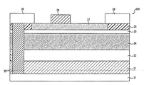
도 1은, 종래의 갈륨 나이트라이드(GaN) 트랜지스터 소자(100)를 나타낸다. 소자(100)는, 예를 들면 실리콘(Si), 실리콘 카바이드(SiC), 사파이어(sapphire) 또는 다른 물질로 구성될 수 있는 기판(11); 각각 두께가 약 0.1㎛ 내지 약 1.0㎛가 되는 알루미늄 나이트라이드(AlN)의 층과 알루미늄 갈륨 나이트라이드(AlGaN)의 층으로 구성될 수 있는, 기판(11) 상에 형성된 1개 이상의 천이층(transition layer)(12); 일반적으로 갈륨 나이트라이드(GaN)로 구성되고 일반적으로 두께가 약 0.5㎛ 내지 약 3㎛가 되는, 1개 이상의 천이층(12) 상에 형성된 버퍼층(buffer layer)(13); 일반적으로 두께가 약 0.01㎛ 내지 약 0.1㎛가 되는 갈륨 나이트라이드(GaN) 또는 인듐 갈륨 나이트라이드(InGaN)로 구성될 수 있는, 전류 전도 채널(current conducting channel)을 제공하기 위하여 버퍼층(13) 상에 형성된 전류 전도성 영역(14); 일반적으로 알루미늄 갈륨 나이트라이드(AlGaN), 알루미늄(Al), 티타늄(Ti), 및 실리콘(Si)으로 구성되고, 일반적으로 두께가 약 0.01㎛ 내지 약 0.03㎛가 될 수 있는, 전류 전도 영역(14) 상에 또는 옆에 형성된 콘택 영역(contact region)(15); 일반적으로, 알루미늄(Al) 대 갈륨(Ga)의 비율이 약 0.1 내지 약 1이 되는 알루미늄 갈륨 나이트라이드(AlGaN)로 구성되는, 전류 전도 영역(14)의 상부 및 콘택 영역(15) 사이에 약 0.01㎛ 내지 약 0.03㎛의 두께로 형성된 장벽층(16); 장벽층(16) 상에 형성되고, 니켈(Ni)과 금(Au) 금속 콘택을 가지며 p형 갈륨 나이트라이드(GaN)로 구성된 게이트 구조(17); 및 니켈(Ni)과 금(Au)과 같은 캡핑(capping) 금속을 구비하며 티타늄(Ti)과 알루미늄(Al)으로 구성될 수 있는, 소스(source) 콘택부와 드레인(drain) 콘택부의 콘택 영역(15) 상에 각각 형성된 저항성 콘택 금속(ohmic contact metal)(18,19)을 포함한다. 전류 전도 영역(14), 콘택 영역(15) 및 장벽층(16)은, 집합적으로, 소자(100)의 전기적 연결 및 제어를 제공하는 소자 층을 형성한다. 1 shows a conventional gallium nitride (GaN)
도 2는, 종래의 또 다른 갈륨 나이트라이드(GaN) 트랜지스터 소자(200)를 나타낸다. 소자(200)는, 기판(21), 천이층(22), 버퍼층(24), 채널층(25), 콘택 영역(26), 장벽층(27), 게이트 구조(28), 및 소스 및 드레인 콘택(29,30)을 포함한다. 이러한 층은, 도 1에 대하여 설명한 것과 유사한 파라미터를 가질 수 있다. 또한, 소자(200)는, 상부 콘택에서부터(즉, 도 2에 도시된 바와 같이, 소스 콘택(30)에서부터 또는 드레인 콘택(29)에서부터) 기판을 포함한 모든 물질층을 거쳐 기판(21)의 저부 상의 금속층(31)까지 연장하는 웨이퍼 관통 비아(through-wafer via)(20)를 갖고 있다. 금속층(31)은, 예를 들면 히트 싱크(heat sink)가 될 수 있다.2 shows another conventional gallium nitride (GaN)
도 3은, 또 다른 갈륨 나이트라이드(GaN) 소자(300)를 나타낸다. 소자(300)는, 기판(41), 천이층(42), 버퍼층(43), 채널층을 포함한 전류 전도 영역(44), 콘택 영역(45), 장벽층(47), 게이트 구조(48), 및 소스 및 드레인 콘택(46,49)을 포함한다. 이러한 층은, 도 1 및 도 2에 대하여 설명한 것과 유사한 파라미터를 가질 수 있다. 소자(300)는, 기판(41)을 소스 콘택(49)에 연결하는 기판 연결 비아(substrate connection via)(40)를 포함한다. 반도체 소자(200)(도 2)의 비아(20)와 달리, 반도체 소자(300)의 비아(40)는 기판(41)의 후면까지 완전히 연장하지 않고 기판(41) 내에서 끝난다.3 shows another gallium nitride (GaN)
도 2 및 도 3과 관련하여 설명하는 것과 같은 비아 연결부는, 반도체 소자의 후면(예를 들어 기판의 후면)에서 소자의 전면 연결부(예를 들어 소스 또는 드레인 콘택, 게이트 구조, 또는 다른 요소(element))까지 매우 낮은 인덕턴스(inductance) 및 낮은 저항의 경로를 제공한다. 이것은, 이러한 소자가 의도하는 고주파 동작에 있어서 중요하다. 종래의 갈륨 나이트라이드(GaN) 트랜지스터 소자(100,200,300)는 단점을 갖고 있다. 소자(100)(도 1)는, 실리콘(Si)과 같은 전도 기판을 사용할 때, 플로팅(floating) 기판 전위(potential)를 가진다. 이것은, 기판 전압이 지나친 양의 전압이 되면, 의도하지 않은 소자 턴온(turn-on)을 초래할 수 있다. 게다가, 음의 기판 전압은 소자(100)의 저항 증가를 초래할 수 있다. 소자(200,300)(도 2 및 도 3)는, 각각의 콘택(30,49)에 각각의 기판(21,41)을 전기적으로 연결함으로써 이러한 문제점을 해소한다. 하지만, 집적 소자에 있어서, 소망하는 기판 전위가 각각의 소자마다 다를 수 있다. 콘택에 기판을 전기적으로 연결하는 것은, 몇몇 집적 소자가 비최적 기판 전위를 갖게 되는 결과를 초래한다.Via connections, such as those described in connection with FIGS. 2 and 3, may be provided at the backside of the semiconductor device (eg, the backside of the substrate) to connect the front side connections of the device (eg, source or drain contacts, gate structures, or other elements). It provides a very low inductance and low resistance path. This is important for high frequency operation intended by such devices. Conventional gallium nitride (GaN)
게다가, 예를 들어 소자(200)(도 2)의 히트 싱크(31)로 도시된 바와 같은, 소자의 후면 상에서 연결된 히트 싱크(heat sink)를 갖는 것이 종종 바람직하다. 개재형 절연성 물질이 히트 싱크(31)와 기판(21) 사이에 포함되어 있지 않으면, 기판(21)을 콘택(30)에 전기적으로 연결하는 것은, 바람직하지 않은 전압이 히트 싱크(31)에 존재하는 결과를 초래할 수 있다. 하지만, 히트 싱크(31)와 기판(21) 사이에 절연성 물질을 포함시키는 것은, 히트 싱크(31)의 효과에 해로울 수 있다. 절연성 물질이 열적 저항을 증가시키고, 히트 싱크(31)와 기판(21) 사이의 절연성 물질은 소자 내에 열을 계속 가지고 있다. 그럼에도 불구하고, 회로를 형성하고 동일한 히트 싱크를 사용하도록 다수의 소자를 사용할 때와 같이, 이러한 물질을 포함하는 것이 종종 필요하게 된다.In addition, it is often desirable to have a heat sink connected on the back side of the device, for example as shown by
히트 싱크(31)와 기판(21) 사이에 절연성 물질을 포함하는 것이 바람직하지 않지만 종종 필요한 일예는, 2개의 갈륨 나이트라이드(GaN) 필드 이펙트 트랜지스터(“FETs”)를 직렬로 연결하여 벅 컨버터(buck converter)를 형성할 때이다. 벅 컨버터의 제1 필드 이펙트 트랜지스터(FET)는, 접지(ground)에 연결된 소스와, 스위치 노드(switch node)에 연결된 드레인을 가지고 있다. 제2 소자는, 스위치 노드에 연결된 소스와, 고전압에 연결된 드레인을 가지고 있다. 따라서 2개의 필드 이펙트 트랜지스터(FET) 소자는, 스위치 노드에서 동일한 전위에 연결되고, 스위치 노드 전압이 접지와 고전위를 번갈아 생기도록 교호로 턴온된다. 전체 기판이 접지(즉, 제1 필드 이펙트 트랜지스터(FET) 소자의 소스 전위)에 연결되면, 제2 소자의 소스는 기판에 비하여 전위가 높아져서 이러한 제2 필드 이펙트 트랜지스터(FET) 소자에서의 매우 큰 저항 증가를 가져온다. 기판 전위가 스위치 노드 전압으로 설정되면, 제1 소자는 소스 아래의 기판에 비하여 높은 음 전위를 가지게 되며, 그 저항이 높아진다.It is not desirable to include an insulating material between the
그러므로 상기 전위를 집적 반도체 소자의 각 콘택 아래의 전위를 독립적으로 제어할 수 있는 한편 또한 상기 반도체 소자의 후면을 독립적인 전위로 설정하는 유연성을 갖는 것이 바람직하다.Therefore, it is desirable to have the flexibility to independently control the potential under each contact of the integrated semiconductor element while also setting the back side of the semiconductor element to an independent potential.
알루미늄 갈륨 나이트라이드(AlGaN), 인듐 갈륨 나이트라이드(InGaN), 및 인듐 알루미늄 갈륨 나이트라이드(InAlGaN)를 포함한 갈륨 나이트라이드(GaN)계의 물질은, 모두 직접형 밴드갭 물질이다. 이것은, 전자(electron)가 정공(hole)과 재결합할 때의 광 생성, 매우 짧은 소수 캐리어 수명(minority carrier lifetime), 및 애벌런치 이벤트(avalanche event) 동안의 급속한 캐리어 생성과 같은 독특한 소자 동작 특성을 가져온다. 후자 특성은, 갈륨 나이트라이드(GaN) 소자가 애벌런치 이벤트가 발생했을때, 제어하기 어렵게 만들고, 일반적으로 부품(part)의 파괴를 가져온다. 반면에, 실리콘(Si)은, 비직접형 밴드갭을 가지고 있어서 매끄럽고 제어된 애벌런치와, 애벌런치 조건 하에서의 안전한 소자 작동을 가능하게 한다.Gallium nitride (GaN) -based materials including aluminum gallium nitride (AlGaN), indium gallium nitride (InGaN), and indium aluminum gallium nitride (InAlGaN) are all direct bandgap materials. This allows for unique device operating characteristics such as light generation when electrons recombine with holes, very short minority carrier lifetimes, and rapid carrier generation during avalanche events. Bring. The latter characteristic makes the gallium nitride (GaN) device difficult to control when an avalanche event occurs and generally results in part breakdown. Silicon (Si), on the other hand, has a non-direct bandgap to enable smooth and controlled avalanche and safe device operation under avalanche conditions.
그러므로 실리콘(Si) 기반 소자의 유리한 애벌런치 능력을, 단일 소자에서의 갈륨 나이트라이드(GaN)의 개선된 속도 및 저항 특성과 조합하는 것이 바람직하다. Therefore, it is desirable to combine the advantageous avalanche capabilities of silicon (Si) based devices with the improved rate and resistance properties of gallium nitride (GaN) in a single device.
이하에서 설명하는 실시예는, 반도체 소자의 일부분의 기판 영역을 그 각각의 소자의 콘택에 독립적으로 연결하는 것을 제공함으로써 위에서 설명한 문제점과 기타 문제점을 해소한다. 이를 달성하기 위하여, 기판과 다른 요소를 서로 격리하는 것을 제공하는 한편, 다른 요소를 전기적으로 연결 가능케 하는, 1개 이상의 이온주입된 웰(well) 또는 확산된 전도 영역과 비아 연결부의 조합을 설명한다. Embodiments described below solve the above and other problems by providing independent connection of a substrate region of a portion of a semiconductor device to a contact of each of the devices. To achieve this, a combination of one or more implanted wells or diffused conduction regions and via connections is provided that provides isolation of the substrate and other elements from one another, while enabling other elements to be electrically connected. .
도 1은, 종래의 갈륨 나이트라이드(GaN) 트랜지스터 소자의 단면도를 도시하고 있다.
도 2는, 웨이퍼 관통 비아를 사용한 종래의 갈륨 나이트라이드(GaN) 트랜지스터 소자의 단면도를 도시하고 있다.
도 3은, 기판 연결 비아를 사용한 종래의 갈륨 나이트라이드(GaN) 트랜지스터 소자의 단면도를 도시하고 있다.
도 4a는, 본 발명의 제1 실시예에 따라 형성된 트랜지스터 소자의 단면도를 도시하고 있다.
도 4b 내지 도 4g는, 도 4a의 트랜지스터 소자를 형성하는 공정을 도시하고 있다.
도 5는, 제2 실시예에 따라 형성된 트랜지스터 소자의 단면도를 도시하고 있다.
도 6은, 제3 실시예에 따라 형성된 트랜지스터 소자의 단면도를 도시하고 있다.
도 7a는, 본 발명의 제4 실시예에 따라 형성된 트랜지스터 소자의 단면도를 도시하고 있다.
도 7b 내지 도 7g는, 도 7a의 트랜지스터 소자를 형성하는 공정을 도시하고 있다.
도 8은, 제5 실시예에 따라 형성된 트랜지스터 소자의 단면도를 도시하고 있다.
도 9a 내지 도 9c는, 제6 실시예에 따라 형성된 트랜지스터 소자의 단면도를 도시하고 있다.
도 10은, 여기에서 설명하는 실시예에 따른 집적 반도체 소자의 단면도를 도시하고 있다.
도 11은, 여기에서 설명하는 실시예에 따른 집적 반도체 소자의 단면도를 도시하고 있다.
도 12는, 여기에서 설명하는 실시예에 따른 집적 반도체 소자의 단면도를 도시하고 있다.
도 13은, 여기에서 설명하는 실시예에 따른 집적 반도체 소자의 단면도를 도시하고 있다.
도 14는, 여기에서 설명하는 실시예에 따른 집적 반도체 소자의 단면도를 도시하고 있다.
도 15는, 여기에서 설명하는 실시예에 따른 집적 반도체 소자의 평면도를 도시하고 있다.
도 16은, 여기에서 설명하는 실시예에 따른 집적 반도체 소자의 평면도를 도시하고 있다.
도 17은, 여기에서 설명하는 실시예에 따른 집적 반도체 소자의 개략도를 도시하고 있다.
도 18은, 여기에서 설명하는 실시예에 따른 집적 반도체 소자의 단면도를 도시하고 있다.
도 19는, 여기에서 설명하는 실시예에 따른 집적 반도체 소자의 단면도를 도시하고 있다.
도 20은, 여기에서 설명하는 실시예에 따른 집적 반도체 소자의 단면도를 도시하고 있다.
도 21은, 여기에서 설명하는 실시예에 따른 집적 반도체 소자의 단면도를 도시하고 있다.
도 22a는, 여기에서 설명하는 실시예에 따른 집적 반도체 소자의 단면도를 도시하고 있다.
도 22b는, 여기에서 설명하는 실시예에 따른 집적 반도체 소자의 단면도를 도시하고 있다.
도 23은, 여기에서 설명하는 실시예에 따른 집적 반도체 소자의 단면도를 도시하고 있다.
도 24는, 여기에서 설명하는 실시예에 따른 집적 반도체 소자의 단면도를 도시하고 있다.
도 25a는, 여기에서 설명하는 실시예에 따른 집적 반도체 소자의 단면도를 도시하고 있다.
도 25b는, 여기에서 설명하는 실시예에 따른 집적 반도체 소자의 단면도를 도시하고 있다.
도 26은, 여기에서 설명하는 실시예에 따른 트랜지스터 소자의 단면도를 도시하고 있다.
도 27은, 여기에서 설명하는 실시예에 따른 집적 반도체 소자의 단면도를 도시하고 있다. 1 illustrates a cross-sectional view of a conventional gallium nitride (GaN) transistor device.
2 illustrates a cross-sectional view of a conventional gallium nitride (GaN) transistor device using wafer through vias.
3 illustrates a cross-sectional view of a conventional gallium nitride (GaN) transistor device using substrate connection vias.
4A illustrates a cross-sectional view of a transistor element formed in accordance with the first embodiment of the present invention.
4B-4G show the process of forming the transistor element of FIG. 4A.
5 shows a cross-sectional view of the transistor element formed in accordance with the second embodiment.
6 shows a cross-sectional view of the transistor element formed in accordance with the third embodiment.
7A shows a cross-sectional view of a transistor element formed in accordance with a fourth embodiment of the present invention.
7B to 7G show a step of forming the transistor element of FIG. 7A.
8 shows a cross-sectional view of the transistor element formed in accordance with the fifth embodiment.
9A to 9C show cross-sectional views of transistor elements formed in accordance with the sixth embodiment.
10 is a sectional view of an integrated semiconductor device according to the embodiment described herein.
11 illustrates a cross-sectional view of an integrated semiconductor device according to the embodiment described herein.
12 illustrates a cross-sectional view of an integrated semiconductor device according to the embodiment described herein.
13 illustrates a cross-sectional view of an integrated semiconductor device according to the embodiment described herein.
14 is a sectional view of an integrated semiconductor device according to the embodiment described herein.
15 shows a plan view of an integrated semiconductor device according to the embodiment described herein.
16 illustrates a plan view of the integrated semiconductor device according to the embodiment described herein.
17 shows a schematic diagram of an integrated semiconductor device according to the embodiment described herein.
18 illustrates a cross-sectional view of an integrated semiconductor device according to the embodiment described herein.
19 is a sectional view of an integrated semiconductor device according to the embodiment described herein.
20 illustrates a cross-sectional view of an integrated semiconductor device according to the embodiment described herein.
21 is a sectional view of an integrated semiconductor device according to the embodiment described herein.
22A illustrates a cross-sectional view of an integrated semiconductor device according to the embodiment described herein.
22B is a sectional view of an integrated semiconductor device according to the embodiment described herein.
FIG. 23 is a sectional view of an integrated semiconductor device according to the embodiment described herein.
24 illustrates a cross-sectional view of an integrated semiconductor device according to the embodiment described herein.
25A illustrates a cross-sectional view of an integrated semiconductor device according to the embodiment described herein.
25B illustrates a cross-sectional view of an integrated semiconductor device according to the embodiment described herein.
26 illustrates a cross-sectional view of a transistor element according to the embodiment described herein.
27 is a sectional view of an integrated semiconductor device according to the embodiment described herein.
이하, 상세한 설명에서, 특정한 실시예를 참조하기로 한다. 이러한 실시예를, 당업자가 실시할 수 있도록 충분히 상세하게 설명하기로 한다. 다른 실시예를 채용할 수 있고, 다양한 구조적인, 논리적인, 및 전기적인 변경을 할 수 있다는 것을 알아야 한다. 또한, 다양한 방법과 공정을 각각 여러 단계를 포함하여 설명한다. 달리 명시하지 않는 한, 설명한 순서로 또는 다른 순서로 단계를 수행할 수 있다는 점을 이해하여야 한다.In the following detailed description, reference is made to specific embodiments. These embodiments will be described in sufficient detail to enable those skilled in the art to practice. It is to be understood that other embodiments may be employed and that various structural, logical, and electrical changes may be made. In addition, various methods and processes will be described, each including several steps. It is to be understood that the steps may be performed in the order described or in other order, unless otherwise noted.
여기에서 설명하는 실시예가 갈륨 나이트라이드(GaN) 반도체 소자를 포함할지라도, 본 발명이 갈륨 나이트라이드(GaN) 반도체 소자에 한정되지 않는다는 점을 이해하여야 한다. 예를 들면, 설명하는 실시예를, 예를 들어 실리콘(Si) 또는 실리콘 카바이드(SiC) 반도체 소자와 게르마늄(Ge) 물질 반도체 소자 등과 같은 다른 전도성 물질을 사용하는 반도체 소자 및 다른 소자에 적용할 수 있다. Although the embodiments described herein include gallium nitride (GaN) semiconductor devices, it should be understood that the present invention is not limited to gallium nitride (GaN) semiconductor devices. For example, the described embodiments can be applied to semiconductor devices and other devices using other conductive materials such as, for example, silicon (Si) or silicon carbide (SiC) semiconductor devices and germanium (Ge) material semiconductor devices. have.
게다가, 이온주입되거나 확산된 전도성 영역 또는 웰을 설명하는 동안, 이것이, 기판 내에 다른 극성의 영역을 제공하는 단지 2개의 공정이라는 점을 이해하여야 한다. 따라서 설명하는 실시예가 이온주입되거나 확산된 영역 또는 웰을 참조할 수 있을지라도, 다른 종류의 반대 극성 영역과 그 제조 방법을 사용할 수 있다는 점을 이해하여야 한다. In addition, while describing the implanted or diffused conductive regions or wells, it should be understood that this is only two processes that provide regions of different polarity in the substrate. Thus, while the described embodiments may refer to ion implanted or diffused regions or wells, it should be understood that other types of opposite polar regions and methods of making the same may be used.
설명하는 실시예는, 주변 층 또는 기판으로부터 1개 이상의 바이어스 극성으로 전기적으로 격리되는 전도성 웰을 갖는, 갈륨 나이트라이드(GaN) 트랜지스터, 또는 트랜지스터를 포함한 집적 회로와 같은 트랜지스터 또는 다른 반도체 소자를 포함한다.Embodiments described include transistors or other semiconductor devices, such as gallium nitride (GaN) transistors, or integrated circuits including transistors, having conductive wells electrically isolated with one or more bias polarities from a peripheral layer or substrate. .
몇몇 실시예에서, 소자는 전도성 기판을 가지며, 상기 기판의 영역은 상기 기판의 것과 반대되는 극성의 전도도로 도핑되어 있다. 반대 극성의 영역은, 예를 들면 p형 기판 내의 n형 물질이다. 상기 소자는, 그 전면(front side)에 있는 콘택에서부터 반대 극성의 영역까지의 관통 비아와 같은 전기적 연결부를 가지고 있다. 다른 실시예에서, 상기 영역은 기판과 같은 도핑 타입을 가질 수 있고, 1개 이상의 절연층으로 둘러 싸여질 수 있다. 다른 실시예에서, 상기 기판이 대체로 비전도성이 될 수 있는 한편, 상기 영역은 p형 또는 n형 도핑을 가지고 있다. 다른 실시예에서, 또한 실리콘 온 인슐레이터(silicon-on-insulator: SOI) 실시예와, 병렬 전도 채널을 포함하는 실시예를 설명한다. 전기적 격리는, 여러 이점 중에서 각 소자의 아래 및/또는 단일 소자 내의 개개의 콘택 아래에 있는 기판이나 다른 물질의 독립적인 제어를 가능하게 한다. In some embodiments, the device has a conductive substrate, and regions of the substrate are doped with conductivity of opposite polarity to that of the substrate. The region of opposite polarity is, for example, an n-type material in a p-type substrate. The device has electrical connections such as through vias from the contacts on its front side to the regions of opposite polarity. In other embodiments, the region may have a doping type, such as a substrate, and may be surrounded by one or more insulating layers. In other embodiments, the substrate may be generally nonconductive while the region has p-type or n-type doping. In another embodiment, a silicon-on-insulator (SOI) embodiment and an embodiment including a parallel conduction channel are also described. Electrical isolation allows for independent control of substrates or other materials below each device and / or below individual contacts within a single device, among other advantages.
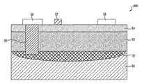
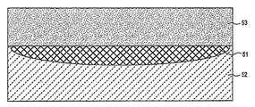
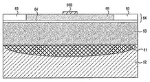
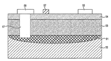
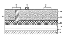
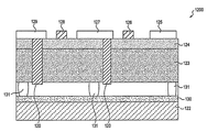
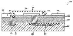
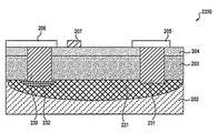
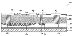
도 4a는, 갈륨 나이트라이드(GaN) 트랜지스터 소자(400)의 단면도를 도시한다. 소자(400)는, 1개 이상의 실리콘(Si), 실리콘 카바이드(SiC), 갈륨 나이트라이드(GaN), 갈륨 아세나이드(GaAs), 알루미늄 나이트라이드(AlN), 및/또는 사파이어 기반 물질로 구성될 수 있는 기판(52); 0.1㎛~0.5㎛ 범위의 두께를 가진 1층 이상의 화합물 반도체 물질(예를 들어 알루미늄 나이트라이드(AlN) 물질), 0.1㎛~2㎛ 두께를 가진 1층 이상의 알루미늄 갈륨 나이트라이드(AlGaN), 및 0.01㎛~5㎛ 두께를 가진 1층 이상의 GaN으로 구성될 수 있는, 기판(52) 상에 형성된 버퍼층(53); 장벽층(16)(도 1)으로서의 역할을 담당하는 15~100% 알루미늄(Al)을 가지며 0.005㎛ 내지 0.03㎛의 두께를 가진 알루미늄 갈륨 나이트라이드(AlGaN)의 층을 포함할 수 있는, 버퍼층(53) 상에 형성된 소자층(54)을 포함한다. 여기에서 실시예의 다른 특징을 설명하는데 있어서 명료함을 위하여 도시하지 않더라도, 소자(400)와의 전기적 연결과 소자(400)의 제어를 제공하는 요소가, 일반적으로, 주 전류 전도 채널을 제공하는 전류 전도 영역(14)과, 콘택(55,56) 중 어느 하나 또는 모두의 아래에 있는 콘택 영역(15)(도 1)을 포함한 소자층(54)에 형성되어 있는 것을 이해하여야 한다. 상기 전류 전도 영역은, 바람직하게는 약 0.01㎛ 내지 약 0.5㎛ 두께의 범위에 있는 갈륨 나이트라이드(GaN) 또는 인듐 갈륨 나이트라이드(InGaN), 또는 공지된 다른 적절한 물질로 구성될 수 있다. 상기 콘택 영역은, 바람직하게는 약 0.01㎛ 내지 약 0.03㎛ 두께의 범위에 있는 실리콘(Si)을 가질 수 있는 알루미늄 갈륨 나이트라이드(AlGaN), 알루미늄(Al) 및 티타늄(Ti), 또는 공지된 다른 적절한 물질로 구성될 수 있다. 또한, 소자층(54)은, 채널층이 2개의 장벽층 사이에 있는 장벽/채널/장벽층 구성을 포함할 수 있다. 4A shows a cross-sectional view of a gallium nitride (GaN)
소자(400)는, 소자층(54) 상에 형성된 콘택(55,56)(예를 들어 소스 콘택 및 드레인 콘택)과 게이트 구조(57)를 포함한다. 콘택(55,56)이 티타늄(Ti) 및 알루미늄(Al)의 혼합물로 구성될 수 있고, 게이트 구조(57)가 p형 갈륨 나이트라이드(GaN)와 티타늄 나이트라이드(TiN) 또는 니켈(Ni)과 금(Au)으로 구성될 수 있다.
또한, 소자(400)는 기판(52) 내에 이온주입된 전도성 웰(51)과, 전도성 웰(51) 내에서 끝나는 연결 비아(50)를 포함한다. 일 실시예에서, 기판(52)은, 1e14 전자/㎤와 1e16 전자/㎤ 사이에서 도핑이 이루어진 n형 기판이 될 수 있고, 전도성 웰(51)은, 1e17 원자/㎤와 1e20 원자/㎤ 사이의 보론(boron) 농도로 보론이 이온주입된 영역으로 구성된 p형 웰이 될 수 있다. 이러한 소자는 기판에 비하여 음의 전위에서 동작한다. 또 다른 실시예에서, 기판(52)이 p형 기판이 될 수 있고 웰(51)이 n형 웰이 될 수 있어서 기판에 비하여 양의 전위에서 동작하는 소자를 제공한다. 또 다른 실시예에서, 전도성 웰(51)이 p형 또는 n형이 될 수 있고, 기판(52)이 대체로 비전도성(즉, 진성(intrinsic)) 기판이 될 수 있다. 다른 극성은 전도성 웰(51)과 기판(52)을 전기적으로 격리한다. 연결 비아(50)가 1㎛ 내지 5㎛ 두께 범위의 알루미늄(Al) 물질로 구성될 수 있고, 또한 0.01㎛ 내지 0.1㎛ 두께 범위의 얇은 층의 티타늄 나이트라이드(TiN)가 비아(50) 내에 또는 상에 사용될 수 있다. 한편, 텅스텐(W) 또는 구리(Cu) 플러그(plug) 기술은, 소형 고종횡비의 비아를 충전하는데 적용될 수 있는 한편, 실리콘(Si) 웰을 콘택하는데 0.01㎛ 내지 0.1㎛ 두께 범위의 얇은 층의 티타늄 나이트라이드(TiN)를 사용한다. 비아(50)를 위하여 텅스텐 또는 구리 기술을 사용하는 능력은, 기존의 전하 결합 소자(“CCD”) 제조 공정 단계를 통합시키는 것이 비아(50)를 형성할 수 있게 한다. The
비아(50)는, 소자(400)의 고주파 동작에 매우 도움이 되는, 반도체 소자(400)의 후면에서 소자의 전면(예를 들어 도시된 바와 같이 전면의 콘택(56))까지 매우 낮은 인덕턴스 및 낮은 저항의 경로를 제공한다. 소자(400)의 후면에 있는 소자층과 버퍼층(54,53) 아래에 웰(51)이 존재하는 것은 후면 전위를 기판 전위로부터 격리시킨다. 기판 전위를 격리하는 이점 중 하나는, 기판(52)의 후면에서 연결된 히트 싱크(31)(도 2)가 소자(400)와 다른 전위 상태로 되는 것을 가능케 하는 것이다.Via 50 has a very low inductance from the back side of
소자(400)의 제조 프로세서를 도 4b 내지 도 4g와 관련하여 설명한다. 도 4b에서, 기판(52)을 예컨대 웨이퍼 기판 상에 제공하고, 이온주입된 웰 영역(51)을 기판(52)의 표면에 형성된다. 이온주입된 웰 영역(51)을, 기판(52) 상에 실리콘(Si) 산화를 실시하고, 포토리소그래피를 사용하여 기판(52) 상에 포토레지스트 패턴 정의(definition)를 형성하고, 이온주입기를 사용하여 고 에너지의 보론 원자와 같은 불순물(dopant)에 기판(52)을 노출시키고, 잔존하는 포토레지스트를 벗겨내고, 고온(예를 들어 1100℃)에서 적절한 기간(예를 들어 3시간) 동안 웨이퍼를 열처리하고, 그 다음에 불화수소 함유 산(acid)에 침지하여 어떠한 표면 산화물이든지를 제거함으로써 형성할 수가 있다.A fabrication processor for
게이트 구조(57)와 소스 및 드레인 콘택(55,56)을 형성하도록, 기판(52) 상에 버퍼층(53), 소자층(54) 및 게이트 구조(57)를 성장시킬 수 있다. 예를 들면, 도 4c에 도시된 바와 같이, 핵 생성 공정 및 성장 공정을 사용하여 기판(52) 상에, 바람직하게는 약 0.1㎛ 내지 약 1.0㎛ 두께의 알루미늄 나이트라이드(AlN) 물질 및/또는 알루미늄 갈륨 나이트라이드(AlGaN) 물질의 1개 이상의 층과, 바람직하게는 약 0.5㎛ 내지 약 3.0㎛ 두께의 갈륨 나이트라이드(GaN) 물질의 1개 이상의 층으로 구성되는 버퍼층(53)을 형성할 수 있다.The
도 4d에 도시된 바와 같이, 그 다음에, 버퍼층(53) 상에 소자층(54)을 형성할 수 있다. 소자층(54)은, 주 전류 채널의 역할을 담당하는 전류 전도성 영역(64) 상에 형성된 장벽층(66)을 포함할 수 있다. 소자층(54)의 형성은, 일반적으로 약 0.01㎛ 내지 약 0.5㎛ 두께의 갈륨 나이트라이드(GaN) 또는 인듐 알루미늄 갈륨 나이트라이드(InAlGaN) 물질의 층을 증착하여 전류 전도 영역(64)을 형성하는 단계와, 알루미늄(Al) 비율(알루미늄(Al) 비율과 갈륨(Ga) 비율의 합이 1이 되는 그러한 알루미늄(Al)의 함량이다)이 약 0.1 내지 약 1.0의 범위에 있고, 두께가 약 0.01㎛ 내지 약 0.03㎛ 범위에 있는 알루미늄 갈륨 나이트라이드(AlGaN)로 구성된 물질의 층을 증착하여 장벽층(66)을 형성하는 단계를 포함할 수 있다. 또한, 소자층(54)은, 층(66) 상에, 마그네슘(Mg)이 도핑된 갈륨 나이트라이드(GaN) 물질의 층을 증착하여 전자 흡수 영역(66b)을 형성하는 단계를 포함할 수 있다. 증착된 장벽층(66)의 측부에 실리콘(Si)을 이온주입함으로써 콘택 영역(65)을 형성할 수 있다.As shown in FIG. 4D, the
도 4e에 도시된 바와 같이, 그 다음에, 소자층(54)(명료함을 위하여 도 4e에서 단일 층으로 도시됨) 상에 게이트 구조(57)와 저항성 콘택(55,56)을 형성한다. 예를 들면, 소자층(54)의 표면 상에(예를 들어 도 4d의 전자 흡수 영역(66b) 상에) p형 갈륨 나이트라이드(GaN) 물질을 증착하고, p형 갈륨 나이트라이드(GaN) 물질에서 게이트 구조(57)를 식각하고, 갈륨 나이트라이드(GaN) 물질 상에 탄탈륨(Ta), 티타늄(Ti), 티타늄 나이트라이드(TiN), 텅스텐(W), 또는 텅스텐 실리사이드(WSi2)와 같은 내화성 금속(refractory metal) 콘택을 형성함으로써 게이트 구조(57)를 형성할 수 있다. 게이트 구조(57)를 제공하는 다른 공지된 방법과 물질을 또한 사용할 수 있다는 것을 이해하여야 한다. 니켈(Ni), 금(Au), 티타늄(Ti) 또는 티타늄 나이트라이드(TiN)와 같은 캡핑(capping) 금속과 함께 티타늄(Ti) 및/또는 알루미늄(Al)과 같은 공지된 어떠한 저항성 콘택 금속이든지로 저항성 콘택(55,56)을 형성할 수 있다. 상기 금속과 게이트 층은, 각각 바람직하게는 약 0.01㎛ 내지 약 1.0㎛ 두께이고, 그 다음에 800℃와 같은 고온에서 60초 동안 열처리된다.As shown in FIG. 4E, a
도 4f에 도시된 바와 같이, 비아(50)의 영역을 제외하고 모든 영역에서 소자층(54)(명료함을 위하여 도 4f에서 단일 층으로 도시됨)을 SiO2와 포토레지스트로 도포하고, 그 다음에 상기 도포된 소자를 식각 챔버(chamber) 내의 고 에너지 플라즈마(plasma)에 노출시킴으로써 연결 비아(50)(도 4g)를 위한 개구부(67)를 형성할 수 있다. 상기 고 에너지 플라즈마는, 일반적으로 BCl3 또는 Cl2와 같은 염소 기반 가스를 포함하고, 이것은 상기 식각 챔버 내에서 만들어진 고주파 발진 전장(high energy oscillating field)을 통하여 형성된다. 상기 소자층과 버퍼층을 식각한 후에, 화학적 스트리퍼(stripper), 산소 플라즈마, 또는 이들 기술의 조합을 사용하여 소자층(54)에서 상기 포토레지스트를 벗겨낸다.As shown in FIG. 4F, the device layer 54 (shown as a single layer in FIG. 4F for clarity) is applied with SiO 2 and photoresist in all regions except the region of the via 50, and The
도 4g에 도시된 바와 같이, 그 다음에, 개구부(67)(도 4f)에 전도성 비아(50)를 형성한다. 개구부(67) 내에 티타늄 나이트라이드(TiN)와 알루미늄(Al)을 증착하여 티타늄 나이트라이드(TiN) 물질이 개구부(67)의 벽을 따라 외부층을 약 100Å~200Å 범위의 두께로 형성하고, 알루미늄(Al) 물질이 약 1㎛~5㎛ 범위의 두께를 가진 비아(50)의 내부층을 형성하는 비아(50)를 형성할 수 있다. 티타늄 나이트라이드(TiN) 외부층은 알루미늄(Al) 물질의 접착성을 증진시킨다. 그 다음에 배선(Routing) 금속을 증착하고 식각하여 비아(50)와, 다른 연결부 예를 들어, 갈륨 나이트라이드 필드 이펙트 트랜지스터(GaN FET)의 소스 콘택 사이에 연결부를 형성한다.As shown in FIG. 4G, a conductive via 50 is then formed in the opening 67 (FIG. 4F). Titanium nitride (TiN) and aluminum (Al) are deposited in the
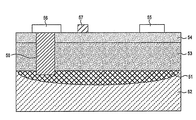
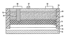
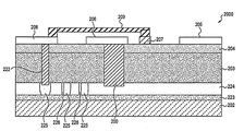
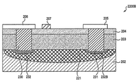
도 5를 참조하면, 기판(52), 버퍼층(53), 소자층(54), 게이트 구조(57), 및 소스 및 드레인 콘택(55,56)을 포함하는 또 다른 반도체 소자(500)가 도시되어 있다. 또한, 소자(500)는 연결 비아(50)와 웰(51)을 포함한다. 이러한 요소는, 도 4의 소자(400)에 대하여 설명한 것과 유사한 파라미터를 가질 수 있으며, 유사한 제조 공정을 통하여 형성될 수 있다.Referring to FIG. 5, another
또한, 소자(500)는, 웰(51)과 기판(52) 사이에 있는 복수의 격리층(58,59.60)을 포함한다. 격리층(58,59.60)은 기판(52)과 웰(51)과 함께 다이오드 구조를 형성한다. 특히, 격리층(58,59.60)이 반대 극성의 층을 형성한 채, 웰(51)과 기판(52)은 동일한 극성(예를 들어 n 또는 p)의 물질이 될 수 있다. 웰(51), 기판(52), 격리층(58,59.60)에 의해 형성되는 다이오드 구조는, 어느 하나의 극성의 전압에 대하여 기판(52)으로부터 웰(51) 전압의 격리를 제공하고, 이로써 소자(500)를, 기판(52)에 비하여 양 또는 음의 전위로 구성할 수 있게 한다. 3개의 격리층이 도 5에 도시되어 있을지라도, 단일 격리층을 포함하여 웰(51)과 기판(52) 사이에 더 많거나 더 적은 격리층이 될 수 있다. 바람직한 실시예에서, 웰(51)과 기판(52) 사이의 1개 이상의 격리층(58,59,60)은, 상기 다이오드 구조의 래치업(latch-up)을 방지하기 위하여 소수 캐리어 재결합 불순물, 예를 들어 백금(Pt)을 포함한다.The
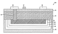
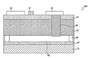
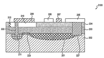
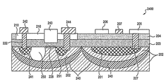
도 6을 참조하면, 기판(52), 버퍼층(53), 소자층(54), 게이트 구조(57), 및 소스 및 드레인 콘택(55,56)을 포함하는 또 다른 반도체 소자(600)가 도시되어 있다. 또한, 소자(600)는 연결 비아(50)와 웰(51)을 포함한다. 이러한 요소는, 도 4의 소자(400)에 대하여 설명한 것과 유사한 변수를 가질 수 있고, 유사한 제조 공정을 통하여 형성될 수 있다.Referring to FIG. 6, another
소자(600)는, 웰(51)과 기판(52)과 함께 사이리스터(thyristor)를 형성하는, 반대 타입으로 도핑된 격리층(68,69)을 포함한다. 예를 들면, 웰(51)은 n형 도핑된 물질이 될 수 있고, 기판(52)은 p형 도핑된 물질이 될 수 있고, 격리층(68)은 n형 도핑된 물질이 될 수 있고, 격리층(69)은 p형 도핑된 물질이 될 수 있어 n-p-n-p 접합을 형성한다. 사이리스터는 양방향 차단형 p-n 접합을 가지는 점에서 특징이 있다. 바람직한 실시예에서, 격리층(68,69) 중의 하나는, 저 도핑된 영역이고, 차단 영역(즉, 격리층(68) 또는 격리층(69)이, 일반적으로 1e14 원자/㎤ 내지 1e16 원자/㎤ 범위의 저 도핑 영역이다)을 형성한다.
소자(600)는, 기판(52)의 후면 전위의 제어를 제공한다. 또한, 형성된 n-p-n-p또는 p-n-p-n 접합은, 어느 하나의 극성의 전압을 격리할 수 있게 하고, 이로써 콘택(55,56)과 게이트 구조(57)를 기판(52)에 비하여 양 또는 음의 전위로 유지할 수 있게 한다. 또 다른 실시예에서, 예를 들면 동일한 타입의 도핑(즉, 둘 다 p형 또는 둘 다 n형)의 웰(51)과 기판(52)을 갖는 것이 바람직하면, 기판(52)과 웰(51) 사이에 제3 격리 영역(미도시)을 추가할 수 있다.
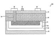
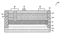
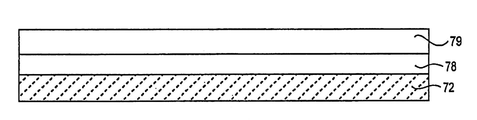
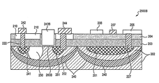
도 7a를 참조하면, 버퍼층(53), 소자층(54), 게이트 구조(57), 소스 및 드레인 콘택(55,56), 및 연결 비아(50)를 포함하는 또 다른 반도체 소자(700)가 도시되어 있다. 이러한 요소는 도 4의 소자(400)에 대하여 설명한 것과 유사한 파라미터를 가질 수 있고, 유사한 제조 공정을 통하여 형성될 수 있다. 또한, 소자(700)는, 소자(600)(도 6)의 기판(52), 격리층(68,69), 웰(51)과 각각 유사한 물질로 구성될 수 있지만 평탄한 층으로 형성되는 기판(72), 격리층(78,79) 및 웰(71)을 포함한다. 또한, 소자(700)는, 이웃한 반도체 소자 간의 격리를 제공하는, 소자(700)의 각 측부 상에 형성되는 격리 영역(70)을 포함한다. 후술하는 바와 같이, 소자(700)의 구조는, 동작면에서 소자(600)와 유사하지만, 제조의 용이성을 제공한다. 일예에서, 실리콘 온 인슐레이터(“SOI”) 물질을 사용하여 소자(700)를 형성할 수 있다. 예를 들면, 층(78)을 SiO2와 같은 절연성 물질로 형성할 수 있고, 층(79)은 SOI 기판의 실리콘(Si)이 될 수 있다.Referring to FIG. 7A, another
소자(700)의 제조 방법을 도 7b 내지 도 7g와 관련하여 설명한다. 여기에서 설명하는 제조 방법을, 개개의 반도체 소자에, 또는 단일 웨이퍼 기판 상의 복수 집적된 반도체 소자에 쉽게 적용할 수 있다는 것을 알아야 한다.The manufacturing method of the
도 7b에서, 기판(72)을 준비하고, 예를 들어 상기한 바와 같이 실리콘(Si) 또는 다른 적절한 물질의 에피택시 증착을 통하여 기판(72) 상에, 또는 전도성 기판(72) 상의 SiO2층(78) 상의 Si층(79)으로 구성되는 SOI 기판 상에 대체로 평탄한 층의 물질로서 격리층(78,79)을 형성한다.In FIG. 7B, the
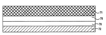
도 7c에서, 그 다음에, 예를 들어 보론이 도핑된 Si 물질의 에피택시 증착을 통하여 격리층(78,79) 상에 웰(71)을 형성한다. 한편, SOI 기판이 소자(700)에 사용되면, 웰(71)의 형성은 기판(72)을 격리하는데 필요하지 않을 수 있다.In FIG. 7C, the
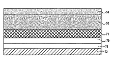
도 7d에서, 그 다음에, 갈륨 나이트라이드(GaN) 물질 또는 다른 적절한 물질을 사용하여 상기한 도 4c 및 도 4d의 버퍼층(53)과 소자층(54)과 관련하여 상기한 바와 유사한 형태로 버퍼층(53)과 소자층(54)을 에피택시법으로 형성할 수 있다.In FIG. 7D, the buffer layer is then in a form similar to that described above in connection with the
도 7e에 도시된 바와 같이, 그 다음에, 도 4e와 관련하여 상기한 방식으로 소자층(54)과 연결 비아(50) 상에 게이트 구조(57)와 저항성 콘택(55,56)을 형성한다.As shown in FIG. 7E, the
도 7f에 도시된 바와 같이, 그 다음에, 도 4f 및 도 4g와 관련하여 상기한 방식으로 소자층(54)과 버퍼층(53)을 거쳐 웰(71) 안으로 연장하는 연결 비아(50)를 형성한다. 한편, SOI 물질이 사용되고, 분리된 웰(71)이 소자(700)에 형성되어 있지 않으면, 비아(50)는 실리콘(Si)층(79) 또는 SiO2층(78) 안으로 연장될 수 있다.As shown in FIG. 7F, a connection via 50 is then formed which extends into the well 71 via the
도 7g에 도시된 바와 같이, 그 다음에, 이웃한 소자로부터 소자(700)의 웰(71)을 격리하기 위하여 격리 영역(70)을 형성할 수 있다. 콘택(55,56)(도 7e)을 형성할 부분 사이의 소자층(54)의 일부분을 포토레지스트로 도포하고, 그 다음에, 노출된 층을, 최소한 웰(71)의 아래까지 바람직하게는 격리층(78)까지 식각함으로써 격리층(70)을 형성할 수 있다. 그 다음에, 식각된 영역을 산화물 또는 다른 적절한 절연 물질로 충전할 수 있다.As shown in FIG. 7G, an
도 8을 참조하면, 실리콘 온 인슐레이터(“SOI”) 구성의 반도체 소자(800)가 도시되어 있다. 소자(800)는, 버퍼층(53), 소자층(54), 소스 및 드레인 콘택(55,56), 및 게이트 구조(57)를 포함한다. 이러한 요소는, 도 6의 소자(600)에 대하여 설명한 것과 유사한 파라미터를 가질 수 있고, 유사한 제조 공정을 통하여 형성될 수 있다. 또한 장치(700)는, 대체로 평탄한 층으로 또는 다른 적절한 형태로 형성될 수 있는 기판(72)을 포함한다.Referring to FIG. 8, a
또한, 소자(800)는, SOI층(89)과, SOI층(89)과 기판(72) 사이의 매몰 산화물 층(82)을 포함한다. SOI층(89)을, 예를 들면 약 1e14 원자/㎤ 내지 1e19 원자/㎤ 범위의 농도로 도핑된 실리콘(Si) 물질로 구성할 수 있다. SOI층(89)은, 소자(800)의 소망하는 구성에 따라 p형 또는 n형 도핑을 가질 수 있다. 소자(800)는, 1개 이상의 소자 콘택(예를 들어, 콘택(55))을 SOI층(89)에 전기적으로 연결하는 연결 비아(80)를 포함한다. 매몰 산화물 층(82)은 기판(72)을 SOI층(89)으로부터 전기적으로 격리시킨다.The
도 8에 도시된 바와 같이, 이웃한 소자의 각 SOI 영역(89)을 격리하도록 격리 이온주입(88)을 사용할 수 있다. SOI층(89)을 형성하도록 사용한 것과 반대로 도핑된 물질로 격리 이온주입(88)을 형성하고, 이로써 이웃한 집적 소자의 각 SOI 영역(89)을 가로질러 전도가 이루어지는 것을 방지한다. 격리 이온주입(88)이 충분히 두꺼우면, 양방향으로 SOI층(89)에 전기적 격리를 제공할 수 있을지라도, SOI층(89)에 반대되는 극성을 갖는 격리 이온주입(88)이 SOI층(89)과 함께 n-p-n 다이오드를 형성할 수 있는 가능성이 있다. 이것은, n-p-n 다이오드가 개방 베이스를 갖게 하여 이웃한 SOI 영역 간의 전도를 일으키는 결과를 초래한다. 따라서 또 다른 실시예에서, 백금(Pt)과 같은 소수 캐리어 수명 단축형 불순물, 또는 공지된 다른 적절한 불순물을 격리 이온주입(88)에 추가할 수 있다.As shown in FIG. 8,
도 9a를 참조하면, 에피택시 기반 기판 격리를 포함하는 또 다른 반도체 소자(900)가 도시되어 있다. 소자(900)는, 소자(700)(도 7a)의 기판(72)과 버퍼층(53)과 유사한 물질로 형성할 수 있는 기판(72)과 버퍼층(94)을 포함한다. 예를 들면, 버퍼층(94)을, 0.1㎛~0.5㎛ 범위의 두께를 가진 알루미늄 나이트라이드(AlN) 물질, 0.1㎛~2㎛의 두께를 가진 1층 이상의 알루미늄 갈륨 나이트라이드(AlGaN), 및 0.01㎛~5㎛ 두께를 가진 갈륨 나이트라이드(GaN)로 구성할 수 있다. 기판(72)을, 1개 이상의 실리콘(Si), 실리콘 카바이드(SiC), 또는 갈륨 아세나이드(GaAs) 기반 물질로 구성할 수 있다.Referring to FIG. 9A, another
소자(900)는, 기판(72) 상에 형성된 1개 이상의 기판 격리층(92)을 포함한다. 기판 격리층(92)을, 알루미늄 나이트라이드(AlN)와 같은 물질, 또는 고 알루미늄(Al) 농도의 알루미늄 갈륨 나이트라이드(AlGaN) 물질, 또는 다른 적절한 물질로 형성할 수 있다. 바람직한 기판 격리층(92)의 두께는, 소자(900)에 요구되는 정격 전압에 의존하고, 바람직하게는 차단하도록 요구되는 매 100V 당 0.5㎛ 내지 1㎛ 범위에 있을 수 있다.
또한, 소자(900)는 주 전류 전도 채널을 제공하는 전류 전도 영역(95)과, 전류 전도 영역(95) 상의 장벽층(96)을 포함한다. 전류 전도 영역(95)은, 갈륨 나이트라이드(GaN), 인듐 갈륨 나이트라이드(InGaN), 또는 공지된 다른 적절한 물질로 구성될 수 있고, 바람직하게는 약 0.01㎛ 내지 약 0.1㎛ 범위의 두께를 가진다. 장벽층(96)을, 바람직하게는 두께가 약 0.01㎛ 내지 약 0.03㎛ 범위에 있으며, 알루미늄(Al) 대 갈륨(Ga) 비율이 바람직하게는 약 0.1 내지 약 1의 범위에 있는 알루미늄 갈륨 나이트라이드(AlGaN), 또는 공지된 다른 적절한 물질로 구성할 수 있다. 실시예의 다른 특징을 설명하는데 있어서 명료함을 위하여 도시하지 않더라도, 소자(900)가, 또한 바람직하게는 약 0.01㎛ 내지 0.03㎛ 범위의 두께를 가진 실리콘(Si) 또는 공지된 다른 적절한 물질을 포함할 수 있는 알루미늄 갈륨 나이트라이드(AlGaN), 알루미늄(Al) 및 티타늄(Ti)으로 구성할 수 있는, 콘택(55,56) 중 어느 하나 또는 모두의 아래에 있는 콘택 영역(15)(도 1)을 포함할 수 있다는 것을 이해하여야 한다. The
또한, 소자(900)는 기판 격리층(92)과 버퍼층(94) 사이에 병렬 채널을 형성하는, 병렬 전류 전도 영역으로서 역할을 담당하는 전도성 웰(93)을 포함한다. 병렬 전류 전도 영역(93)을, 1e17 Si/㎤ 내지 1e19 Si/㎤ 범위로 실리콘(Si)을 도핑한 n형 갈륨 나이트라이드(GaN) 물질로 형성할 수 있다. 또 다른 실시예에서, 전류 전도 영역(95)을 형성하는 방식과 유사하게 병렬 전류 전도 영역(93)을 알루미늄 갈륨 나이트라이드(AlGaN) 물질로 갈륨 나이트라이드(GaN) 물질의 상부면 상에 형성할 수 있다. 나이트라이드 물질의 피에조 효과(Piezo effect) 때문에, 각각의 알루미늄 갈륨 나이트라이드(AlGaN)층의 하단부에 2DEG가 형성된다. 이러한 실시예에서, 알루미늄 갈륨 나이트라이드(AlGaN) 물질은, 바람직하게는 약 0.02㎛ 내지 0.03㎛ 범위의 두께와, 약 20% 내지 30% 범위의 알루미늄(Al) 농도를 가진다. 갈륨 나이트라이드(GaN) 물질은, 바람직하게는 약 0.1㎛의 두께를 가진다. The
또한, 소자(900)는, 전류 전도 영역(95)과 병렬 전류 전도 영역(93) 사이의 버퍼층(94) 내에 있는 채널 연결부(90)를 포함한다. 채널 연결(90)을, 바람직하게는 약 1e17 원자/㎤ 내지 1e19 원자/㎤ 범위의 밀도로 버퍼층(94)에 실리콘(Si) 원자를 이온주입함으로써 형성할 수 있다. 다른 실시예에서, 채널 연결부(90)를, 티타늄 나이트라이드와 함께 텅스텐 또는 알루미늄으로 구성할 수 있다. 또한, 소자(900)는 선택적으로, 소자(700)(도 7)의 격리 영역(70)과 유사한 물질로 구성할 수 있으며 유사한 방식으로 형성할 수 있거나, 다른 적절한 물질과 공정으로 구성하고 형성할 수 격리 영역(97)을 포함할 수 있다. 예를 들면, 격리 영역(97)을, 최소한 병렬 전류 전도 영역(93) 아래의 깊이로, 바람직하게는 기판 격리층(92) 안으로 소자(900)의 외측 부분을 식각하고, 그 식각된 부분을 산화물로 충전함으로써 형성할 수 있다.The
도 9b는, 시뮬레이션(920)에서 도시된 종래의 반도체 소자(예를 들어 도 1의 소자(100))와, 시뮬레이션(930)에서 도시된 반도체 소자(900) 간의 시뮬레이션된 전도 경로의 비교를 나타내고 있다. 시뮬레이션(920)은, 단일 채널을 제공하는 단일 전류 전도 영역(14)이 버퍼층(13) 상에 형성되는 반도체 소자의 전도 경로를 보여준다. 시뮬레이션(930)은, 주 전류 전도 영역(95), 버퍼층(94), 병렬 채널을 형성하는 병렬 전류 전도 영역(93), 및 기판 격리층(92)을 갖는 반도체 소자(900)와 같은 반도체 소자의 전도 경로를 보여준다.9B shows a comparison of a simulated conduction path between a conventional semiconductor device (eg,
도 9c는, 시뮬레이션(920,930)의 전류 전도 경로(940,950)의 비교를 각각 그래픽 형태로 나타낸다. 도 9c의 전류 전도 경로(940)는, 전류가 전류 전도 영역(14)의 1개의 주 채널을 통하여 흐르는 것을 나타내는 한편, 전류 전도 경로(950)는, 전류가 제1 주 전류 전도 영역(95)의 주 채널에서 버퍼층(94)을 거쳐 병렬 전도 영역(93)의 병렬 채널로 흐르는 것을 나타낸다.9C shows, in graphical form, a comparison of the
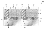
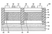
도 10을 참조하면, 집적 반도체 소자(1000)가 도시되어 있다. 집적 소자(1000)는, 단일 기판(102) 상에 집적된 2개의 이웃한 반도체 소자, 즉 콘택(105,107)과 게이트(016)에 의해 제어되는 제1 소자와, 콘택(108,110)과 게이트(109)에 의해 제어되는 제2 소자를 포함한다. 제1,2 반도체 소자는, 예를 들면 도 4a에 관련하여 상기한 반도체 소자(400)와 유사한 갈륨 나이트라이드(GaN) 반도체 소자가 될 수 있다. 예를 들면, 소자(1000)에서, 기판(102)을, 1개 이상의 실리콘(Si), 실리콘 카바이드(SiC), 갈륨 아세나이드(GaAs), 및/또는 사파이어 기반 물질로 구성할 수 있다. 버퍼층(103)을, 0.1㎛ 내지 0.5㎛ 범위의 두께를 가진 알루미늄 나이트라이드(AlN) 물질, 0.1㎛ 내지 2㎛ 범위의 두께를 가진 1층 이상의 알루미늄 갈륨 나이트라이드(AlGaN), 0.01㎛ 내지 5㎛ 범위의 두께를 갈륨 나이트라이드(GaN)로 구성할 수 있다. 소자층(104)을, 0.01㎛ 내지 0.03㎛ 범위의 두께를 가지며, 약 15%~30% 범위의 알루미늄(Al) 농도를 가진 알루미늄 갈륨 나이트라이드(AlGaN)로 구성할 수 있다. 콘택(105,107,108,110)을, 티타늄(Ti)과 알루미늄(Al)의 혼합물로 구성할 수 있다. 게이트 구조(106,109)를, p형 갈륨 나이트라이드(GaN)와 티타늄 나이트라이드(TiN) 또는 니켈(Ni)과 금(Au)으로 구성할 수 있다. 유사한 특성을 가진 반도체 소자가 제조의 용이성과 기타 이점을 제공할 수 있을지라도, 집적 소자(1000) 내의 각 반도체 소자를 위한 각각의 구성 요소가 동일하거나 유사한 특성을 가질 필요가 없다는 점을 이해하여야 한다.Referring to FIG. 10, an
집적 소자(1000)는, 각각의 반도체 소자 아래에 있는 각각의 웰 영역(101)과, 각각의 반도체 소자의 콘택(110,107)에서 각각의 웰 영역(101)까지 이어지는 각각의 연결 비아(100)를 포함한다. 상기한 바와 같이, 기판(102)은 n형 기판이 될 수 있고, 이온주입된 웰(101)은 p형 웰이 될 수 있어 기판(102)에 비하여 음의 전위에서 동작하는 소자를 제공한다. 또 다른 실시예에서, 기판(102)은 p형 기판이 될 수 있고, 웰 영역(101)은 n형 웰이 될 수 있어 기판(102)에 비하여 양의 전위에서 동작하는 소자를 제공한다. 비아(100)를, 비아(100)를 완전히 충전하는 SiO2뿐 아니라 1㎛ 내지 5㎛ 범위의 두께를 가진 알루미늄(Al) 물질과, 0.01㎛ 내지 0.1㎛ 범위의 두께를 가진 얇은 층의 티타늄 나이트라이드(TiN)로 구성할 수 있다.The
집적 소자(1000)에서, 비아(100)는, 반도체 소자의 후면에서 상기 소자의 전면 연결부(예를 들어 콘택(107,110))까지 매우 낮은 인덕턴스와 낮은 저항의 경로를 제공한다. 이러한 특성은, 고주파 동작에 도움이 될 수 있다. 소자 아래에 웰(101)이 존재하고, 버퍼층(104,103)이 소자(1000)의 후측에 존재하는 것은, 이러한 특성을 제공하는 한편, 또한 기판 전위로부터 후면 전위를 격리시킨다. 따라서 집적 소자(1000)의 각각의 반도체 소자는, 각각의 게이트, 소스 및 드레인 콘택(105-110)의 전위로부터뿐만 아니라 기판 전위로부터 격리되는 독립적으로 제어하는 후면 전위를 가지고 있어 완전히 독립적인 반도체 소자를 제공한다.In the
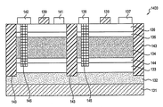
집적 소자(1000)가 중대한 이점을 제공할지라도, 전도성 웰(101)의 하나의 잠재적인 문제점은, 이웃한 웰이, 웰(101) 사이에서 래치업으로 알려진 바람직하지 못한 단락 상태를 일으킬 수 있는 n-p-n 또는 p-n-p 접합을 형성할 수 있다는 것이다. 도 11을 참조하면, 또 다른 집적 소자(1100)는, 소자(1000)(도 10)에 관하여 상기한 것과 유사한 요소를 포함하고, 또한 집적 소자(1100)의 이웃한 반도체 소자의 각각의 웰(101) 사이에 있는 억제 영역(111)을 포함한다. 억제 영역(111)은, 소수 캐리어 재결합 영역으로서 구성할 수 있고, 백금(Pt) 또는 다른 적절한 재결합 중심 물질을 사용하여 형성할 수 있다. 억제 영역(111)은, 이웃한 각각의 웰(101) 간의 래치업(latch-up) 상태를 억제한다.Although
도 12를 참조하면, 실리콘 온 인슐레이터(“SOI”) 구성을 가진 집적 반도체 소자(1200)가 도시되어 있다. 소자(1200)는 버퍼층(123)과 소자층(124)을 포함한다. 이러한 요소는, 상기한 소자(800)(도 8)에 대하여 설명한 것과 유사한 파라미터를 가질 수 있으며, 유사한 제조 공정을 통하여 형성될 수 있다. 또한, 소자(1200)는, 상기한 소자(800)(도 8)에 대하여 설명한 것과 유사한 파라미터를 가질 수 있으며 유사한 제조 공정을 통하여 형성될 수 있는, 기판(122), SOI층(121), 버퍼층(123)과 기판(122) 사이의 매몰 산화물 층(130)을 포함한다. 소자(1200)는, 전기적 콘택(예를 들어 소스 콘택(129,127))을 SOI층(121)에 연결하는 연결 비아(120)를 포함한다. 매몰 산화물 층(130)은, 상기 SOI층으로부터 기판(122)을 전기적으로 격리하여 기판 전압을 상기 SOI층 전압에 대해 독립적으로 되게 한다. Referring to FIG. 12, an
소자(1200)는, 소스 및 드레인 콘택(125,127,129)과 게이트 구조(126,128)를 포함한다. 이 실시예에서, 집적 소자(1200)의 2개의 이웃한 반도체 소자는, 소스 콘택(129)에 대하여 드레인으로서 역할을 담당하며, 드레인 콘택(125)에 대하여 소스로서 역할을 담당하는 공통 콘택(127)을 공유하여 하프브릿지(half-bridge) 회로 소자를 형성한다.
격리 이온주입(131)은, 집적 소자(1200)의 각각의 트랜지스터 소자에 해당하는 SOI층(121)의 영역을 격리하는데 사용된다. 격리 이온주입(131)을, SOI층(121)을 형성하도록 사용한 것과 반대되는 타입으로 도핑한 물질로 형성하고, 이로써 이웃한 집적 소자의 SOI 영역을 가로질러 전도가 이루어지는 것을 방지한다. 소자(800)에 관하여 상기한 바와 같이, 다른 실시예에서는, 격리 이온주입(131)에, 백금(Pt) 또는 공지된 다른 어떠한 적절한 불순물과 같은 소수 캐리어 수명 단축 불순물을 추가할 수 있다.The
도 13을 참조하면, 병렬 채널 구성의 집적 반도체 소자(1300)가 도시되어 있다. 소자(1300)는, 반도체 소자(900)(도 9)와 같은 복수의 반도체 소자를 포함한다. 집적 소자(1300)는, 집적 소자(1300)의 각 반도체 소자마다 각각의 주 채널을 제공하는 제1 전류 전도 영역(135)과, 각각의 주 채널(135) 위에 및 콘택(137,138,141,142) 아래에 있는 장벽층(136)을 포함한다. 이들 요소는, 상기한 소자(900)(도 9)와 유사한 특성을 포함할 수 있고, 유사한 공정을 통하여 형성될 수 있다.Referring to FIG. 13, an
또한, 집적 소자(1300)는, 기판 격리층(132)과 버퍼층(134) 사이의 각 소자마다 각각의 병렬 전도 채널을 형성하는 전도성 웰(133)을 포함한다. 병렬 전류 전도 영역(133)을, 소자(900)(도 9)에 관하여 상기한 바와 같이, 갈륨 나이트라이드(GaN) 물질의 상부면 상에 알루미늄 갈륨 나이트라이드(AlGaN) 물질이 있는, 실리콘(Si) 도핑의 n형 갈륨 나이트라이드(GaN) 물질, 또는 다른 적절한 반도체 물질로 형성할 수 있다. 버퍼층(134)의 각각의 채널 연결부(140)를, 전류 전도 영역(135)과 병렬 전류 전도 영역(133) 사이에 형성한다. 채널 연결부(140)를, 바람직하게는 약 1e17 원자/㎤ 내지 1e19 원자/㎤ 범위의 밀도로, 더욱 바람직하게는 약 1e18 원자/㎤의 밀도로, 실리콘(Si) 원자를 버퍼층(134)에 선택적으로 이온주입하고, 1150℃에서 2시간 동안 열처리함으로써 형성할 수 있다. 바람직하게는, 전류 전도 영역(135), 병렬 전류 전도 영역(133), 및 채널 연결부(140)는 모두 n형 물질이다. 각각의 전류 전도 영역(135)과 병렬 전류 전도 영역(133)은, 채널 연결부(140)를 통하여 전기적으로 연결된다.The
또한, 집적 소자(1300)는, 기판(131) 상에 형성된 1개 이상의 기판 격리 영역(132)을 포함한다. 기판 격리 영역(132)을, 알루미늄 나이트라이드(AlN), 또는 고 알루미늄(Al) 함량의 알루미늄 갈륨 나이트라이드(AlGaN) 물질, 또는 다른 적절한 물질과 같은 물질로 형성할 수 있다. 소자(900)(도 9)에 관하여 상기한 바와 같이, 바람직한 기판 격리층(132)의 두께를, 집적 소자(1300)에 요구되는 정격 전압에 따라 변경할 수 있다.The
또한, 소자(1300)는, 선택적으로, 소자(700)(도 7)의 격리 영역(70)과 유사한 물질로 구성할 수 있으며 유사한 방법으로 형성할 수 있거나, 다른 적절한 물질로 구성할 수 있으며 다른 적절한 공정으로 형성할 수 있는 격리 영역(143)을 포함한다. 예를 들면, 격리 영역(143)을, 소자의 지정된 부분을 최소한 병렬 전류 전도 영역(133) 아래의 깊이로, 바람직하게는 기판 격리층(132) 안으로 식각하고, 상기 식각된 부분을 산화물로 충전함으로써 형성할 수 있다. 채널 연결부(140)는, 반도체 소자의 후면에서 소자의 전면 연결부(예를 들어 콘택(142,138))까지 매우 낮은 인덕턴스와 낮은 저항의 경로를 제공하는 한편, 이웃한 소자 사이와 소자의 후면에 있는 기판 격리층(132) 사이에 격리 영역(143)이 존재하는 것이, 각각의 반도체 소자가, 기판의 전위로부터 및 이웃한 소자의 채널의 전위로부터 격리되는, 독립적으로 제어되는 후면 전위를 가질 수 있게 한다.In addition, the
도 14를 참조하면, 도 13과 관련하여 상기한 반도체 소자(1300)와 유사한 다수의 반도체 소자를 포함하는, 병렬 채널 구성을 가진 또 다른 집적 반도체 소자(1400)가 도시되어 있다. 또한, 집적 소자(1400)는, 병렬 전류 전도 층(133)과 버퍼층(134) 사이에 있는 백(back) 장벽층(144)을 포함한다. 백 장벽층은, 높은 알루미늄(Al) 함량의 알루미늄 갈륨 나이트라이드(AlGaN) 또는 알루미늄 나이트라이드(AlN) 물질로 구성될 수 있다. 병렬 전류 전도 층(133)과 버퍼층(134) 사이에 백 장벽층(144)을 제공하는 것은, 전자가 병렬 전류 전도 영역(133)에서 콘택(137,138,141,142)으로 이동하는 것을 방지함으로써 집적 소자(1400)의 항복 전압을 증가시킨다.Referring to FIG. 14, there is shown another
또한, 집적 반도체 소자(1400)는, 금속으로 구성되고, 병렬 전류 전도 영역(133)에서 콘택(138,142)까지 연장하는 금속 채널 연결부(145)를 포함한다. 금속 채널 연결부(145)는, 높은 알루미늄(Al) 함량의 알루미늄 갈륨 나이트라이드(AlGaN) 물질에 실리콘(Si)을 이온주입하는 것이, 비전도성 물질을 초래할 수 있고, 이로써 불량 연결을 초래할 수 있기 때문에, 병렬 전류 전도 층(133)을 위한 높은 알루미늄(Al) 함량의 물질을 사용하는 소자를 위한 다른 타입의 채널 연결부(즉, 실리콘(Si) 채널 연결부)보다 이점을 제공할 수 있다. 금속 채널 연결부(145)를, 집적 소자(1400)를 표면에서 병렬 전류 전도 영역(133)까지 금속 채널 연결부(145)의 선택된 부분을 식각하고, 상기 식각된 부분을 금속으로 충전함으로써 형성할 수 있다. 금속 채널 연결부(145)를 충전하도록 사용하는 금속은, 티타늄(Ti), 알루미늄(Al), 티타늄 나이트라이드(TiN), 텅스텐(W), 또는 다른 적절한 금속, 또는 그 조합과 같은, 콘택(137,138,141,142)에 사용하는 동일한 금속이 될 수 있다.The
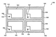
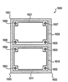
도 15를 참조하면, 집적 반도체 소자(1500)의 평면도가 도시되어 있다. 집적 반도체 소자(1500)는, 단일 기판(1500) 상에 집적된 4개의 개별 반도체 소자(1551,1552,1553,1554)를 포함한다. 집적 반도체 소자(1500)의 각각의 반도체 소자는, 각각의 이온주입 웰(51)(도 4)이 표면 아래에 각각 형성되는 각각의 이온주입 영역(1502,1505,1508,1511)과, 소자층(54)(도 4)과 전기적 연결부(예를 들어 도 4의 콘택(55,57) 및 게이트(56))가 각각의 소자마다 형성되는 활성 소자 영역(1503,1506,1509,1512)을 포함한다. 각각의 이온주입 영역(1502,1505,1508,1511) 내이지만 각각의 활성 소자 영역(1503,1506,1509,1512)의 외부에는, 각각의 이온주입 웰에서 각각의 반도체 소자의 전면 연결부(예를 들어, 소스 및/또는 드레인 콘택)까지 매우 낮은 인덕턴스와 낮은 저항의 경로를 제공하도록 사용할 수 있는 비아(1501,1504,1507,1510)가 있다. 반도체 소자(1551,1552,1553,1554)는, 도 1 내지 도 14 중 어느 것이든지를 참조하여 상기한 바와 같은 반도체 소자를 포함할 수 있고, 바람직하게는 도 4 내지 도 14 중 어느 것이든지를 참조하여 상기한 바와 같은 1개 이상의 반도체 소자를 포함할 수 있다. 도 4 내지 도 14에 관하여 상기한 특성을, 기판 전위와 격리되는 독립적으로 제어되는 후면 전위, 및/또는 이웃한 소자의 것과 격리되는 전도 영역을 각각의 반도체 소자에 제공하도록 사용할 수 있다. Referring to FIG. 15, a plan view of an
도 16을 참조하면, 또 다른 집적 반도체 소자(1600)의 평면도가 도시되어 있다. 집적 반도체 소자(1600)는, 단일 기판 상에 집적된 2개의 개별적인 반도체 소자(1651,1652)를 포함한다. 각각의 반도체 소자는, 반도체 소자(1651,1652)를 위한 연결부에 비아(1601~1608)가 있는 다수개(이 경우에, 4개)의 활성 영역(1610,1620)을 포함한다. 반도체 소자(1651,1652)는 도 1 내지 도 14를 참조하여 설명한 바와 같은 반도체 소자를 포함할 수 있고, 바람직하게는 도 4 내지 도 14를 참조하여 설명한 바와 같은 1개 이상의 반도체 소자를 포함할 수 있다. 도 4 내지 도 14에 관하여 상술한 특징을, 기판 전위로부터 격리되는 독립적으로 제어되는 후면 전위, 및/또는 이웃한 소자의 것으로부터 또는 동일한 소자 내의 다른 전도 영역으로부터 격리되는 전도 영역을 각각의 반도체 소자에 제공하도록 사용할 수 있다.Referring to FIG. 16, a plan view of another
상기한 반도체 소자는, 다양한 용도로 사용될 수 있다. 예를 들면, 상기한 구조와 공정을, 집적 회로의 일부분으로서 동작하는 활성 소자를 기판에 형성하도록 사용할 수 있다. 이러한 소자의 일반적인 카테고리(category)는, 다이오드, 바이폴라 접합 트랜지스터(“BJT”), 및 필드 이펙트 트랜지스터(“FET”)를 포함할 수 있다.The semiconductor device may be used for various purposes. For example, the structures and processes described above can be used to form active elements on a substrate that operate as part of an integrated circuit. General categories of such devices may include diodes, bipolar junction transistors (“BJTs”), and field effect transistors (“FETs”).
도 17을 참조하면, 집적 반도체 소자의 예의 개략도가 도시되어 있다. 개략도는, (a) 단일 트랜지스터, (b) 하프브리지(half bridge)를 형성하도록 직렬로 연결된 1쌍의 트랜지스터, (c) 풀브리지(full bridge)를 형성하도록 연결된 4개 트랜지스터의 그룹, 및 (d) 3상브리지(3phase bridge))를 형성하도록 연결된 6개 트랜지스터의 그룹을 포함한다. 병렬로 형성된 트랜지스터의 그룹(즉, (c) 구성으로 도시됨)은, 고속 스위칭 회로를 형성하는데 사용될 수 있다.Referring to FIG. 17, a schematic diagram of an example of an integrated semiconductor device is shown. The schematic diagram includes (a) a single transistor, (b) a pair of transistors connected in series to form a half bridge, (c) a group of four transistors connected to form a full bridge, and ( d) group of six transistors connected to form a three phase bridge). A group of transistors formed in parallel (ie, shown in (c) configuration) can be used to form a high speed switching circuit.
도 18을 참조하면, 집적 갈륨 나이트라이드(GaN) 반도체 소자(1800)가 도시되어 있다. 소자(1800)는, 상기한 물질과 공정을 사용하여 형성할 수 있는, 기판(202), 버퍼층(203), 및 소자층(204)을 포함한다. 또한, 소자(1800)는, 상기한 물질과 공정을 사용하여 형성할 수 있는, 소자층(204) 상에 형성된 드레인 콘택(205), 소스 콘택(206), 및 게이트 구조(207)를 포함한다. 또한, 소자(1800)는, 소자(1800)의 후면에 있는 기판(202)에 형성된 웰(201)에 소스 콘택(206)을 연결하는 비아(200)를 포함한다.Referring to FIG. 18, an integrated gallium nitride (GaN)
또한, 소자(1800)는, 게이트 웰이라고 부를 수 있는 기판(202)의 제2 전도성 웰(211) 사이에 형성된 게이트 보호 다이오드를 포함한다. 게이트 보호 다이오드는, 비아(212), 게이트 패드(208), 및 금속 배선(209)(또는 다른 구조)을 통하여 게이트 구조(207)에 연결된다. 게이트 보호 다이오드는, 게이트 구조(207)를, 게이트 산화물 항복 전압을 초과할 수 있는 고전압으로부터 보호한다. 게이트 패드(208)는, 격리 영역(210)에 의해 소자층(204)으로부터 격리되는 소자(1800)의 영역 상에 형성된다. 격리 영역(210)을, 소망하는 영역의 소자층(204)을 식각하고/하거나, 전도를 방지하도록 소자층(204)에 손상을 주는 니켈(Ni), 철(Fe), 바나듐(V)과 같은 고 에너지 원자를 가진 물질, 또는 다른 적절한 물질을 소자층(204)의 상기 영역에 이온주입함으로써 형성할 수 있다. 게이트 구조(207)와 게이트 패드(208)를 연결하는 금속 배선(209)을, 예를 들어 실리콘(Si)이 도핑된 알루미늄(Al) 및/또는 구리(Cu)로 구성할 수 있다. 한편, 금속 배선(209)을, 상기한 드레인 및 소스 콘택(205,206)을 만드는데 사용하는 동일한 금속 물질, 또는 제조 공정에서 나중에 고온을 적용해야 할 때 사용에 특히 도움이 될 수 있는 다결정 실리콘(Si) 물질로 형성할 수 있다.The
비아(212)는, 게이트 패드(208)에서 게이트 웰(211)까지 연장된다. 게이트 웰(211)은, 전도성 웰 영역이고, 바람직하게는 기판(202)과 반대로 도핑되는 물질이다. 예를 들면, 게이트 웰(211)을 n형 물질로 구성할 수 있고, 기판(202)은 p형 기판이 될 수 있음으로써 게이트 보호 다이오드로서 p-n 제너다이오드(Zener diode)를 게이트 웰(211)과 기판(202) 사이에 형성할 수 있다. 바람직한 일 실시예에서, 게이트 웰(211)을, p형 기판(202) 상에 위치하는 고농도 도핑된 p형 물질 상에 고농도 도핑된 n형 물질로 구성할 수 있다. 이러한 다이오드를, 임계 전압이 도달할 때까지 게이트 패드(208)와 기판(202) 사이에서의 전류 흐름을 차단하도록 사용할 수 있고, 그 후에 전류가 게이트 패드(208)와 기판(202) 사이에서 흐른다. 게이트 구조(207) 상의 음의 전압은, 작은 바이어스 상태에서 순방향 바이어스된 p-n 다이오드로부터 전류를 생기게 한다. 게이트 구조(207)를 소스 콘택(206)에 연결할 수 있는 종래의 게이트 보호 다이오드와 달리, 소자(1800)에 도시된 구성은, 과잉 전류가 소스 콘택(206)으로보다는 비아(200,212)를 거쳐 기판(202)으로 흐를 수 있게 한다.Via 212 extends from
도 18을 참조하여 설명한 소자(1800)는, 소자(1800)의 게이트 구조(207)와 다른 요소에 대하여 보호를 제공하는 동안, 전류가 게이트 보호 다이오드를 흐르는 전압이 게이트 구조(207)와 기판(202) 사이의 전압에 기반으로 하기 때문에 문제점이 발생할 수 있다. 따라서 기판(202)의 바이어싱은 독립성을 어느 정도 잃는다. The
도 19를 참조하면, 또 다른 집적 반도체 소자(1900)가 도시되어 있고, 게이트 보호 다이오드가 웰(221) 내에 포함된 게이트 웰(211)에 의해 형성되어 있다. 게이트 보호 다이오드의 게이트 보호 전압을, 게이트-기판 바이어스(도 18의 소자(1800)에서와 같음) 대신에 소자(1900)의 게이트-소스 바이어스에 의해 설정하고, 이로써 독립적인 기판 바이어스를 가능하게 한다. 도 19에 도시되지 않았더라도, 웰(221)을 기판(202)과 버퍼층(203)으로부터 더 격리하도록 도 1 내지 도 17에 관하여 상기한 격리 기술 및 구조를 사용할 수 있다는 것을 알아야 한다.Referring to FIG. 19, another
도 20을 참조하면, 또 다른 집적 반도체 갈륨 나이트라이드(GaN) 반도체 활성 소자(2000)가 도시되어 있다. 소자(2000)는, 게이트 보호 회로를 형성하도록 SOI층(224) 내의 직렬로 연결된 다수의 순방향 바이어스된 다이오드를 포함한다. 소자(2000)는, 기판(202), 매몰 산화물 층(223), 및 SOI층(224)을 포함하는 SOI 기판상에 형성되어 있다.Referring to FIG. 20, another integrated semiconductor gallium nitride (GaN) semiconductor
SOI층(224)은 n형 물질이 될 수 있다. 전도성 영역(225)과 터널 영역(226) 사이의 접합이 터널형 구성을 형성하도록 SOI 층(224) 내에 다이오드를 (예를 들어 p형)이온주입된 전도성 영역(225)과 고농도 도핑된(예를 들어 n형) 터널(tunnel) 영역(226)으로 형성한다. 터널형 콘택은, p-n 접합의 도핑이 매우 높아서(예를 들면 약 1e20 원자/㎤) 전압을 차단할 수 없는 콘택이다. 이러한 콘택은, n영역의 전자가 p형 영역의 밸런스 밴드(valence band) 안으로 직접적으로 이동(즉, 터널링)할 수 있을 때에 발생할 수 있다. 따라서 p-n 접합이 존재할지라도, 그것은, 저항성 또는 전도성 연결과 같이 나타난다. 바람직한 일 실시예에서, 직렬로 연결된 5개의 다이오드가 약 5V의 전압 강하를 만들도록, 각각의 다이오드는 약 1V의 전압 강하를 형성할 수 있다.The
SOI 기판이 소자(2000)의 제조비용을 증가시킬 수 있을지라도, 상기한 구성은, 다른 구성보다 더 적은 이온주입 단계를 필요로 하고, 기판(202)로부터의 자연적인 격리를 소자(2000)의 활성 요소에 제공한다.Although the SOI substrate may increase the manufacturing cost of the
도 21을 참조하면, 또 다른 집적 GaN 반도체 활성 소자(2100)가 도시되어 있다. 소자(2100)는, p형 기판이 될 수 있는 기판(202)과, n형 이온주입된 전도성 웰이 될 수 있는 전도성 웰(201) 및 게이트 웰(211)을 포함한다.Referring to FIG. 21, another integrated GaN semiconductor
소자(2100)는, 게이트 웰(211)과 웰(201) 사이에 백 채널 영역(228)이 형성되는 리세스형 필드 이펙트 트랜지스터(recessed FET) 소자를 형성하도록 게이트 유전체로서 사용하는 다수의 갈륨 나이트라이드(GaN)층을 포함한다. 소자(2100)를, 종래의 MOSFET 소자와 유사하게 동작하도록 구성할 수 있다. 소자(2100)에서, 웰 영역(201)과 게이트 웰 영역(211)이 리세스형 FET의 드레인과 소스로서 각각 기능하는 한편, 게이트 패드(208)는 리세스형 FET의 게이트로서 기능한다. 비아(222)가 게이트 패드(228)를 게이트 웰(211)에 단락시키고, 비아(227)가 웰(201)을 기판(202)에 단락시킨다. 이러한 구성에서, 웰(201)은 매몰 FET의 소스로서 기능한다. 게이트 패드(208)의 인가된 전위는, 백 채널 영역(228)에, 리세스형 FET를 “온(on)”상태로 전환시키는 전자의 축적(accumulation)을 야기하여 연결부(205) 또는 기판(202)과 게이트 패드(208) 사이에서 전류가 흐를 수 있게 하고, 게이트 패드(208)에 존재하는 전압을 제한한다.The
도 22a를 참조하면, 또 다른 집적 갈륨 나이트라이드(GaN) 반도체 활성 소자(2200)가 도시되어 있다. 소자(2200)는, 2개의 비아(230,231)가 전도성 웰(221) 안으로 연장하는 갈륨 나이트라이드 필드 이펙트 트랜지스터(GaN FET) 소자이다. 소스 콘택(206)에 연결된 제1 비아(230)는, 전도성 웰(221) 내에 형성된 저항성 영역(232) 안으로 연장된다. 전도성 웰(221)을 형성하도록 사용하는 동일한 캐리어 타입을 가진 물질(즉, n형 또는 p형 물질)의 고농도 이온주입을 사용하여 저항성 영역(232)을 형성할 수 있다. 예를 들면, 전도성 웰(221)을, 약 1e16 원자/㎤의 농도를 가진 p형 물질로 형성할 수 있고, 저항성 영역(232)을 약 5e18 원자/㎤의 농도로 형성할 수 있다. 드레인 콘택(205)에 연결된 제2 비아(232)는, 전도성 웰(221) 안으로 연장하여 전도성 웰(221)과 쇼트키(Schottky) 콘택을 이룬다.Referring to FIG. 22A, another integrated gallium nitride (GaN) semiconductor
소자(2200)의 역방향 바이어스 상태 동안(예를 들어, 드레인 콘택(205)이 소스 콘택(206)에 비하여 양의 바이어스이고, 게이트 구조(207)가 제로(0) 바이어스일 때), 전도성 웰(221)과 영역(231)에 의해 형성된 쇼트키 다이오드가, 비아(231)에서 웰 영역(221) 안으로의 전류 흐름을 차단한다. 드레인 콘택(205)의 바이어스가 소스 콘택(206)의 바이어스에 비하여 음이 될 때, 전류가 저항성 영역(232)과 전도성 웰(221)을 통하여 드레인 콘택(205)까지 흐르는 한편, 게이트 바이어스는 계속 제로(0)이다(그리고 필드 이펙트 트랜지스터(FET)는 계속“오프(off)”상태이다).During the reverse bias state of device 2200 (eg, when
소자(2200)는, 게이트(207)가 전력 손실이 더 적은 "오프"일 때, 소스 콘택(206)과 드레인 콘택(205) 사이의 전류 흐름을 제공한다. 예를 들면, 갈륨 나이트라이드 필드 이펙트 트랜지스터(GaN FET)의 종래의 문턱 전압은 약 2.1V가 될 수 있다. 반면에, 소스 콘택(206)이 비아(230)에 의하여 전도성 웰(221)에 전기적으로 연결되어 있는 한, 영역(231)과 웰(221)에 의해 형성되는 다이오드 양단의 전압 강하가 단지 약 0.7V이다. 따라서 정전류를 위해, 게이트가 “오프” 상태에 있는 소자(2200)의 전류 흐름은, 종래의 갈륨 나이트라이드 필드 이펙트 트랜지스터(GaN FET) 소자 양단의 전압 강하의 약 36%가 되는 전압 강하를 가져온다.
도 22b를 참조하면, 또 다른 집적 갈륨 나이트라이드(GaN) 반도체 활성 소자(2200B)가 도시되어 있다. 소자(2200B)는, 소자(2200)와 관련하여 설명한 것과 유사한 특징을 포함할 뿐 아니라 비아(231) 아래의 웰(221) 내에 형성된 제2 저항성 영역(232B)을 포함한다. 전도성 웰(221)과 저항성 영역(232)을 형성하도록 사용하는 반대 캐리어 타입을 가진 물질(즉, n형 또는 p형 물질)의 고농도 이온주입을 사용하여 제2 저항성 영역(232B)을 형성함으로써 PIN 접합을 형성할 수 있다.Referring to FIG. 22B, another integrated gallium nitride (GaN) semiconductor
도 23을 참조하면, 또 다른 집적 갈륨 나이트라이드/실리콘(GaN/Si) 반도체 소자(2300)가 도시되어 있다. 소자(2300)는, 버퍼층 (203)을 게이트 절연체로서 사용하는 리세스형 실리콘(Si) FET를 포함한다. 소자(2300)는, 소자(2100)(도 21)에 관하여 상기한 요소와 유사한 물질 및 공정으로 형성할 수 있는, 기판(202), 버퍼층(203), 소자층(204), 콘택(205,206), 게이트 구조(207), 및 전도성 웰(201)을 포함한다. 또한, 소자(2300)는, 또한 소자(2100)(도 21)에 관하여 상기한 요소와 유사한 물질과 공정으로 형성할 수 있는, 격리 영역(210), 제1 비아(222), 제2 비아(227), 실리콘(Si) FET 웰(241), 및 전도성 웰(201)과 실리콘(Si) FET 웰(241) 사이의 백 채널 영역(228)을 포함한다. 또한, 소자(2300)는 실리콘(Si) FET의 독립적인 드레인과 게이트 구조를 포함한다. 실리콘(Si) 게이트 구조(243)와 실리콘(Si) FET 드레인(242)은, 소자(1800)(도 18)에 관하여 상기한 게이트 패드(208)와 유사한 물질과 공정으로, 또는 공지된 다른 적절한 물질과 공정으로 형성할 수 있다.Referring to FIG. 23, another integrated gallium nitride / silicon (GaN / Si)
소자(2300)는, 억제 영역(111)(도 11), 격리 이온주입(131)(도 12), 또는 격리 영역(143)(도 13)과 같은, 도 4 내지 도 22에 관하여 상기한 1개 이상의 격리 구성을 나타내는 격리 구조(240)를 더 포함한다. 하지만, 격리 구조(240)는 공지된 종래의 격리 기술뿐만 아니라 상기한 다른 어떠한 격리 구성물을 이용하여 나타낼 수 있다는 것을 이해하여야 한다.The
도 24를 참조하면, 또 다른 집적 갈륨 나이트라이드/실리콘(GaN/Si) 반도체 소자(2400)가 도시되어 있다. 소자(2400)는, 상기한 물질과 공정으로 형성할 수 있는, 기판(202), 버퍼층(203), 소자층(204), 콘택(205.206), 갈륨 나이트라이드(GaN) 게이트 구조(207), 및 전도성 웰(201)을 포함한다. 또한, 소자(2400)는, 또한 상기한 물질과 공정으로 형성할 수 있는, 격리 영역(210), 비아(222), 비아(227), FET 웰(241), 및 전도성 웰(251)과 FET 웰(241) 사이의 백 채널 영역(228)을 포함한다.Referring to FIG. 24, another integrated gallium nitride / silicon (GaN / Si)
소자(2400)는, 소자층(204)과 버퍼층(203) 안으로 리세스되는 독립적인 MOS 게이트(243)뿐만 아니라 독립적인 필드 이펙트 트랜지스터(FET) 소스(244) 및 드레인(242) 콘택을 포함한다. 게이트(243)를, 버퍼층(203) 내의 알루미늄 나이트라이드(AlN) 핵생성(nucleation) 층에 도달할 때까지 소자층(204)을 거쳐 버퍼층(203)을 부분적으로 식각함으로써 형성할 수 있다. 갈륨 나이트라이드(GaN)의 선택적 식각은, 식각 단계 동안에 O2를 추가하거나, 다른 어떠한 적절한 공정을 통하여 달성할 수 있다.
또한, 소자(2400)는 필드 이펙트 트랜지스터(FET) 웰(241)과 백 채널 영역(228) 사이의 저농도 도핑된 공핍(depletion) 영역(250)을 포함한다. 바람직하게는, 공핍 영역(250)은, 필드 이펙트 트랜지스터(FET) 웰(241)과 필드 이펙트 트랜지스터(FET) 소스 웰(251)(예를 들어 웰(241,251)을 1e17/㎠ 내지 1e19/㎠로 도핑할 수 있다)보다 낮은 불순물 레벨(예를 들어 약 1e14/㎠ 내지 1e17/㎠의 범위)을 가진다. 이것은, 집적 실리콘(Si) FET의 항복 전압을 상승시킨다. 소자(2400)는, 시모스(CMOS: complementary metal oxide semiconductor)형 회로가 가능하도록, 실리콘(Si) 내의 p채널 트랜지스터를 갈륨 나이트라이드(GaN) 내의 n채널 트랜지스터와 통합하는 능력을 제공한다. 예를 들면, n형 웰을 형성하도록 4~8e16/㎤의 농도로 안티몬으로 이온주입함으로써 웰(202)을 형성할 수 있다. p형 드리프트(drift) 웰을 형성하도록 영역(250)에 1e17/㎤의 보론을 이온주입하여 최종적인 2e16/㎤의 p형 도핑을 가진 드리프트 웰을 가져올 수 있다. 고농도 도핑된 저항성 콘택 영역을 형성하도록 영역(241,251)을 1e18/㎤의 보론으로 이온주입할 수 있다. 콘택(242)에 인가된 실리콘 필드 이펙트 트랜지스터(Si FET) 드레인 전압이 음이고, 백 채널 영역(228)이 “오프” 상태일 때, 드리프트 웰(250)과 웰(202) 사이에 형성된 p-n 접합은 전압을 차단한다. 게이트(243)의 음 바이어스는 영역(228)에 정공의 축적을 가져와서 소자를 “온”으로 전환시킨다. 그 다음에, 전류는, 연결부(244)로부터 p형 웰(251), 백 채널 영역(228)을 거쳐 드리프트 웰(250)에 흘러들어가고, 콘택 영역(241)과 연결부(242)를 거쳐 흘러나간다.
또한, 소자(2400)는, 전도성 웰(201)과 웰(241,251)을 분리하는 격리 구조(240)를 포함한다. 도 24의 격리 구조(240) 각각은, 억제 영역(111)(도 11), 격리 이온주입(131)(도 12), 또는 격리 영역(143)(도 13)과 같은 도 4 내지 도 22에 관하여 상기한 1개 이상의 격리 구성을 나타낸다. 격리 구조(240)는 공지된 종래의 격리 기술뿐 아니라 상기한 다른 어떠한 격리 구성으로 나타낼 수 있다는 것을 이해하여야 한다.The
도 25a를 참조하면, 또 다른 집적 갈륨 나이트라이드/실리콘(GaN/Si) 반도체 소자(2500)가 도시되어 있다. 소자(2500)는, 소자(2400)(도 24)에 관하여 위에서 설명한 것과 유사한 요소를 포함하고, 이들 요소의 설명을 생략하도록 한다. 또한, 소자(2500)는, 실리콘(Si) 게이트(243) 주위에 있는 고 유전율(“하이케이(high-K)")의 유전성 물질(260)을 포함한다. 하이케이의 유전성 물질(260)은, 게이트 구조를 형성하는데 일반적으로 사용되는 실리콘 이산화물 또는 유사한 물질보다 더 높은 유전율을 가진 물질을 의미한다. 하이케이의 유전성 물질(260)을 추가하는 것은, 게이트 커패시턴스를 증가시키는 한편, 전류 누설의 가능성을 줄인다. 하이케이의 유전성 물질(260)을, 공지된 적절한 물질로 형성할 수 있고, 바람직하게는 알루미늄 하프늄 실리케이트, 알루미늄 하프늄 디옥사이드와 같은 AlHfSiOx 물질 패밀리 내의 물질로 형성한다. 하이케이의 유전성 물질(260)에서의 알루미늄(Al), 하프늄(Hf), 및 실리콘(Si)의 가장 적합한 조성을 가변할 수 있다. 게이트 구조(243)의 형성 전에, 예를 들어 원자층 증착(atomic layer deposition: ALD), 플라즈마 강화 화학적 기상 증착(Plasma-enhanced chemical vapor deposition: PECVD), 또는 다른 적절한 증착법과 같은 방법을 사용하여 저온에서 하이케이의 유전성 물질(260)을 증착할 수 있다. 소자(2500)의 또 다른 실시예에서, 실리콘(Si) 게이트 구조(243)에서 유사한 이점을 제공하도록, 실리콘(Si) 산화법, 또는 유전체의 증착과 결합된 저온 산화법을 사용할 수 있다.Referring to FIG. 25A, another integrated gallium nitride / silicon (GaN / Si)
도 25b에 도시된 또 다른 실시예에서, 소자(2500B)는, 하이케이의 절연체(260B)가 버퍼층(203)을 완전히 관통하여 식각된 게이트 구조(243B)를 포함한다. 이것은, 하이케이의 게이트 산화물과 게이트 구조(243) 사이에 버퍼층이 존재하지 않고 형성되는 게이트 구조를 초래한다. 장점은, 소자를 턴온시키는데 필요한 저 게이트 전압을 포함하고, 리세스 처리 단계를 비아(222) 식각 단계와 조합하여 제조의 비용 및 복잡성을 줄일 수 있다.In another embodiment, shown in FIG. 25B,
도 26을 참조하면, 또 다른 갈륨 나이트라이드(GaN) 트랜지스터 소자(2600)가 도시되어 있다. 소자(2600)는, 예를 들면 실리콘(Si), 실리콘 카바이드(SiC), 또는 다른 반도체 물질이 될 수 있는 기판(302)과, 제1 비아(300)에 의해 소스 콘택(308)에 연결되는, 기판(302)에 형성된 전도성 웰(301)을 포함한다. 전도성 웰(301)은, 소자층(308)의 활성 부분 아래에 위치하는 영역을 커버한다. 또한, 소자(2600)는, 전도성 웰(301)을 둘러싸는 영역에 저항성 콘택을 이루어 이웃하는 저항성 웰(305)을 형성하는 제2 비아(307)를 포함한다. 전도성 웰(301)과 저항성 웰(305) 사이에 있는 기판(302)의 이온주입되지 않은 부분이 저농도 도핑된 물질이 되도록, 전도성 웰(301)을, 고농도 도핑된 p형 실리콘(Si) 물질로 형성할 수 있고, 저항성 웰(305)을 고농도 도핑된 n형 실리콘(Si) 물질로 형성할 수 있다.Referring to FIG. 26, another gallium nitride (GaN)
소자(2600)는, 드레인 콘택(306)으로의 고전압 스파이크(spike)로부터 소자(2600)를 보호하도록, 기판(302)의 반도체 특성을 유익하게 사용한다. 전도성 웰(301), 저항성 웰(305), 전도성 웰(301)과 저항성 웰(305) 사이의 기판(302)의 부분은, 핀 다이오드(pin diode)를 형성한다. 드레인 콘택(306)에서의 고전압 스파이크 동안에, 전도성 웰(301)과 저항성 웰(305) 사이에 형성된 핀 다이오드는, 애벌런치 상태를 겪게 되어 전하를 기판(302)을 거쳐 전도성 웰(301)에 전송하는 것을 유발한다. 고전압 스파이크의 에너지가, 소자(2600)의 손상이나 파괴를 초래할 수 있는 임계 전압에 도달하기 전에, 핀 다이오드 양단의 애벌런치 상태를 트리거(trigger)하도록 전도성 웰(301), 저항성 웰(305), 기판(302)을 도핑할 수 있다. 소자(2600)와 전도성 웰(301) 및 저항성 웰(305)을 이웃한 구조와 소자로부터 격리하기 위하여, 도 1 내지 도 25에 관하여 상기한 격리 구조를 또한 소자(2600)에 포함할 수 있다는 것을 이해하여야 한다. The
도 27을 참조하면, 또 다른 집적 갈륨 나이트라이드(GaN) 반도체 활성 소자(2700)가 도시되어 있다. 소자(2700)는, 비아 연결부(400,473,473)를 사용하는, 갈륨 나이트라이드(GaN) 소자 내에 집적된 바이폴라 트랜지스터 소자를 포함한다. 집적 소자(2700)의 갈륨 나이트라이드(GaN) 부분을, 상기한 실시예에 따라 형성하고 동작시킬 수 있는, 갈륨 나이트라이드(GaN) 드레인(466), 갈륨 나이트라이드(GaN) 소스(468), 및 갈륨 나이트라이드(GaN) 게이트(469)에 의해 형성한다. 소자(2700)에서, 웰(401)은, 갈륨 나이트라이드(GaN) 소자의 소자층(204)의 활성 영역 아래의 부분의 SOI층(224)에 위치하고 있으며, 갈륨 나이트라이드(GaN) 소자의 후면 전위를 격리시킨다.Referring to FIG. 27, another integrated gallium nitride (GaN) semiconductor
도 27에 도시된 바와 같이, 소자(2700)는, 소자(2000)(도 20)에 관하여 상기한 바와 같은 SOI 절연 구조를 포함한다. 일 실시예에서, 웰(401)은 p형 웰이고, SOI층(224)은 n형 물질로 형성되어 있다. 하지만, 도 1 내지 도 26 중 어느 것이든지에 관하여 상기한 어떠한 격리이든지를 대신에 또는 추가로 사용할 수 있다는 것을 이해하여야 한다. 또한, 다른 실시예에서, 소자(2700)는, 웰(401)을 포함하지 않을 수 있거나, 다른 타입의 후면 격리를 포함할 수 있다.As shown in FIG. 27,
집적 소자(2700)의 바이폴라 부분을, 바이폴라 드레인 콘택(472)과 바이폴라 베이스 콘택(471)에 의해 형성한다. 도 27에 도시되지 않았을지라도, 억제 영역(111)(도 11), 격리 이온주입(131)(도 12), 또는 격리 영역(143)(도 13)과 같은, 도 4 내지 도 26에 관하여 상기한 1개 이상의 격리 구성에 의해 소자층(204)의 활성 갈륨 나이트라이드(GaN) 부분으로부터 바이폴라 베이스 콘택(471)과 바이폴라 드레인 콘택(472)을 격리시킬 수 있다.The bipolar portion of the
집적 소자(2700)의 바이폴라 부분은, 비아(473,474)를 사용하여 매몰된다(buried). 1e16/㎤의 내지 1e19/㎠ 범위의 농도를 가진 이온주입된 웰(470)을 사용하여 소자(2700)의 바이폴라 드레인(472)을 형성하고, 비아(474)가 바이폴라 드레인 콘택(472)에서부터 그 안으로 연장한다. 웰(470)은, n형 SOI층(224) 내에서 p형 물질이 될 수 있다. 다른 실시예에서, 콘택을 더 개선하도록 바이폴라 베이스 연결부(471) 아래에 있는 또 다른 웰(미도시)을 이온주입하거나, 항복 전압을 증가시키도록 웰(401)을 고 도핑된 영역과 저 도핑된 영역으로 구성할 수 있다. 일예는, SOI층이 1e17/㎤의 밀도로 비소가 도핑된 채, 1e18/㎤ 밀도의 보론으로 이온주입한 웰 영역(401,470)이다. 연결 비아(474)가 상기 SOI층에 콘택을 이루는 한편, 비아(400,474)는 컬렉터 및 에미터 영역(401,470)에 각각 연결된다. 연결부(471)에 음의 바이어스가 인가될 때, 상기 SOI층은 에미터 및 컬렉터 영역(470,401)에 비하여 음의 바이어스 상태가 된다. 그 다음에, 정공이 웰(401,470) 사이의 SOI층을 통하여 전도된다.Bipolar portions of
상기 설명 및 도면은, 여기에서 설명한 특징과 장점을 달성하는 특정한 실시예의 예시로서 간주되어야만 한다. 특정한 공정 조건을 변경하고 치환할 수 있다. 따라서 본 발명의 실시예를, 전술한 설명 및 도면에 의해 한정하는 것이 아니라 청구범위의 구성 요소에 의해서만 한정되는 것으로 간주한다.The foregoing description and drawings are to be regarded as illustrative of particular embodiments that achieve the features and advantages described herein. Certain process conditions can be changed and substituted. Accordingly, the present invention is not to be limited by the foregoing description and drawings, but is to be considered limited only by the elements of the claims.
Claims (45)
화합물 반도체 물질을 포함하는 1개 이상의 내부층;
전류 전도 영역을 포함하는 소자층-상기 소자층은 갈륨 나이트 라이드를 포함-;
상기 소자층 상에 형성된 1개 이상의 콘택; 및
상기 내부층을 통하여 상기 콘택에 전기적으로 연결되는 전도성 웰을 포함하고,
상기 전도성 웰은 주위의 물질로부터 1개 이상의 바이어스 극성으로 전기적으로 격리되어 있는 것을 특징으로 하는 트랜지스터 소자.
Board;
At least one inner layer comprising a compound semiconductor material;
An element layer comprising a current conducting region, the element layer comprising gallium nitride;
At least one contact formed on the device layer; And
A conductive well electrically connected to the contact through the inner layer,
And the conductive well is electrically isolated from the surrounding material by at least one bias polarity.
상기 전도성 웰은 상기 주위의 물질과 반대되는 극성의 도핑을 갖는 것을 특징으로 하는 트랜지스터 소자.
The method of claim 1,
And the conductive well has a doping of a polarity opposite to the surrounding material.
상기 전도성 웰이 도핑을 갖고,
상기 주위의 물질은 거의 미도핑되어 있는 것을 특징으로 하는 트랜지스터 소자.
The method of claim 1,
The conductive well has doping,
And the surrounding material is substantially undoped.
상기 1개 이상의 내부층의 화합물 반도체 물질은:
알루미늄 나이트라이드;
알루미늄 갈륨 나이트라이드; 및
갈륨 나이트라이드를 포함하는 것을 특징으로 하는 트랜지스터 소자.
The method of claim 1,
The compound semiconductor material of the at least one inner layer is:
Aluminum nitride;
Aluminum gallium nitride; And
A transistor device comprising gallium nitride.
상기 기판은:
실리콘;
실리콘 카바이드;
사파이어;
알루미늄 나이트라이드;
갈륨 나이트라이드; 및
갈륨 아세나이드 중에서 1개 이상을 포함하는 것을 특징으로 하는 트랜지스터 소자.
The method of claim 1,
The substrate comprising:
silicon;
Silicon carbide;
Sapphire;
Aluminum nitride;
Gallium nitride; And
A transistor device comprising at least one of gallium arsenide.
상기 기판 상에 형성된 절연층, 및 상기 절연층 상에 형성된 도핑된 전도성 물질을 더 포함하는 것을 특징으로 하는 트랜지스터 소자.
The method of claim 1,
And an insulating layer formed on the substrate, and a doped conductive material formed on the insulating layer.
상기 주위의 물질은 p형 기판을 포함하고, 상기 전도성 웰은 n형 물질을 포함하는 것을 특징으로 하는 트랜지스터 소자.
The method of claim 1,
Wherein the surrounding material comprises a p-type substrate and the conductive well comprises an n-type material.
상기 주위의 물질은 n형 기판을 포함하고, 상기 전도성 웰은 p형 물질을 포함하는 것을 특징으로 하는 트랜지스터 소자.
The method of claim 1,
And wherein the surrounding material comprises an n-type substrate and the conductive well comprises a p-type material.
상기 주위의 물질은 거의 비전도성이고, 상기 전도성 웰은 전도성 물질을 포함하는 것을 특징으로 하는 트랜지스터 소자.
The method of claim 1,
And wherein the surrounding material is substantially non-conductive and the conductive well comprises a conductive material.
상기 전도성 웰은 상기 기판 내에 이온주입된 전도성 물질을 포함하는 것을 특징으로 하는 트랜지스터 소자.
The method of claim 1,
And the conductive well comprises a conductive material implanted into the substrate.
상기 전도성 웰은 상기 기판 상에 형성된 전도성 물질의 층을 포함하는 것을 특징으로 하는 트랜지스터 소자.
The method of claim 1,
And the conductive well comprises a layer of conductive material formed on the substrate.
상기 소자층의 상부면에서 상기 전도성 웰까지 연장하여 상기 콘택을 상기 전도성 웰에 전기적으로 연결하는 전도성 비아(via)를 더 포함하는 것을 특징으로 하는 트랜지스터 소자.
The method of claim 1,
And a conductive via extending from the top surface of the device layer to the conductive well to electrically connect the contact to the conductive well.
상기 전도성 비아가 텅스텐 또는 구리를 포함하는 것을 특징으로 하는 트랜지스터 소자.
The method of claim 12,
And the conductive via comprises tungsten or copper.
상기 전도성 비아가 알루미늄, 실리콘, 또는 금을 포함하는 것을 특징으로 하는 트랜지스터 소자.
The method of claim 12,
And the conductive via comprises aluminum, silicon, or gold.
복수개의 전도성 웰을 더 포함하는 것을 특징으로 하는 트랜지스터 소자.
The method of claim 12,
The transistor device further comprises a plurality of conductive wells.
상기 소자층 상에 형성된 소스 콘택 및 드레인 콘택; 및
상기 소자층 상의 상기 소스 콘택과 상기 드레인 콘택 사이에 형성된 게이트 구조를 더 포함하며,
상기 복수개의 전도성 웰은 핀 다이오드를 형성하고, 각각의 전도성 웰은 상기 소스 콘택과 상기 드레인 콘택에 전기적으로 연결되는 것을 특징으로 하는 트랜지스터 소자.
16. The method of claim 15,
A source contact and a drain contact formed on the device layer; And
A gate structure formed between the source contact and the drain contact on the device layer;
And the plurality of conductive wells form a pin diode, each conductive well being electrically connected to the source contact and the drain contact.
상기 소자층 상에 형성된 소스 콘택 및 드레인 콘택; 및
상기 소자층 상의 소스 콘택과 드레인 콘택 사이에 형성된 게이트 구조를 더 포함하며,
상기 복수개의 전도성 웰이 직렬의(series) P-N 다이오드를 형성하고, 각각의 전도성 웰은 상기 소스 콘택과 상기 드레인 콘택 및 상기 게이트 구조 중 하나에 전기적으로 연결되는 것을 특징으로 하는 트랜지스터 소자.
16. The method of claim 15,
A source contact and a drain contact formed on the device layer; And
A gate structure formed between the source contact and the drain contact on the device layer;
And wherein the plurality of conductive wells form a series PN diode, each conductive well being electrically connected to one of the source contact, the drain contact, and the gate structure.
상기 직렬의 P-N 다이오드 내의 교호하는(alternating) P-N 다이오드가 터널 접합을 포함하는 것을 특징으로 하는 트랜지스터 소자.
18. The method of claim 17,
And an alternating PN diode in said series of PN diodes comprises a tunnel junction.
상기 복수개의 전도성 웰 중 1개 이상이 전도성 비아와 쇼트키 연결을 이루는 것을 특징으로 하는 트랜지스터 소자.
16. The method of claim 15,
At least one of the plurality of conductive wells forms a Schottky connection with a conductive via.
상기 복수개의 전도성 웰 중 1개 이상이 전도성 비아와 연결 상태에 있는 저항성 영역을 포함하는 것을 특징으로 하는 트랜지스터 소자.
16. The method of claim 15,
At least one of said plurality of conductive wells comprises a resistive region in connection with a conductive via.
상기 기판과 상기 전도성 웰 사이에 형성된 복수개의 전도성 층을 더 포함하고, 상기 복수개의 전도성 층은 교호하는 도핑 극성을 갖는 것을 특징으로 하는 트랜지스터 소자.
The method of claim 1,
And a plurality of conductive layers formed between the substrate and the conductive wells, the plurality of conductive layers having alternating doping polarities.
상기 소자층 내의 제1 전류 전도 영역; 및
상기 전도성 웰 내의 제2 전류 전도 영역을 더 포함하는 것을 특징으로 하는 트랜지스터 소자.
The method of claim 1,
A first current conducting region in the device layer; And
And a second current conducting region in said conductive well.
상기 내부층을 통과하여 연장하며, 상기 제1 전류 전도 영역 및 제2 전류 전도 영역에 연결하는 채널 연결부를 더 포함하는 것을 특징으로 하는 트랜지스터 소자.
The method of claim 22,
And a channel connection extending through the inner layer and connecting to the first current conducting region and the second current conducting region.
상기 채널 연결부는, 텅스텐, 티타늄 나이트라이드를 가진 알루미늄, 또는 실리콘 중 하나 이상을 포함하는 것을 특징으로 하는 트랜지스터 소자.
24. The method of claim 23,
And the channel connection part comprises one or more of tungsten, aluminum with titanium nitride, or silicon.
상기 트랜지스터 소자는 복수개의 트랜지스터 소자를 포함하는 집적회로의 일부분인 것을 특징으로 하는 트랜지스터 소자.
The method of claim 1,
And the transistor element is part of an integrated circuit comprising a plurality of transistor elements.
상기 트랜지스터 소자 아래에 있는 각각의 기판은 1개 이상의 극성으로 전기적으로 격리되어 있는 것을 특징으로 하는 트랜지스터 소자.
26. The method of claim 25,
Each substrate beneath the transistor element is electrically isolated with at least one polarity.
상기 집적회로는 각각의 트랜지스터 소자마다 복수개의 각각의 전류 전도 영역을 포함하고, 상기 복수개의 각각의 전류 전도 영역은 격리 구조에 의해 서로 격리되어 있는 것을 특징으로 하는 트랜지스터 소자.
26. The method of claim 25,
And said integrated circuit comprises a plurality of respective current conducting regions for each transistor element, said plurality of respective current conducting regions being isolated from each other by an isolation structure.
상기 복수개의 트랜지스터 소자는 제2 트랜지스터 소자를 포함하며,
상기 제2 트랜지스터 소자는:
또 다른 각각의 전류 전도 영역에 전기적으로 연결된 상기 소자층 상에 형성된 콘택; 및
상기 내부층을 통하여 상기 제2 트랜지스터 소자의 콘택에 전기적으로 연결된 제2 전도성 웰을 포함하는 것을 특징으로 하는 트랜지스터 소자.
26. The method of claim 25,
The plurality of transistor elements include a second transistor element,
The second transistor device is:
A contact formed on said device layer electrically connected to each other current conducting region; And
And a second conductive well electrically connected to a contact of the second transistor element through the inner layer.
상기 격리 구조는 각각의 전류 전도 영역을 분리하도록 전류 전도 층 내에 형성된 다이오드를 포함하는 것을 특징으로 하는 트랜지스터 소자.
28. The method of claim 27,
And the isolation structure comprises a diode formed in the current conducting layer to separate each current conducting region.
상기 다이오드는 제1 도핑 극성을 가진 이온주입된 전도성 영역과 제2 도핑 극성을 가진 터널 영역을 포함하는 것을 특징으로 하는 트랜지스터 소자.
30. The method of claim 29,
And the diode comprises an ion implanted conductive region having a first doping polarity and a tunnel region having a second doping polarity.
상기 복수개의 트랜지스터 소자 중 2개 이상이 공통(common) 콘택을 공유하는 것을 특징으로 하는 트랜지스터 소자.
26. The method of claim 25,
At least two of the plurality of transistor elements share a common contact.
소스 콘택, 드레인 콘택, 및 금속 산화물 반도체 게이트 구조를 더 포함하고, 상기 금속 산화물 반도체 게이트 구조는 전자를 축적하기 위한 백(back) 채널 영역 상에 배치되어 있는 것을 특징으로 하는 트랜지스터 소자.
The method of claim 1,
And a source contact, a drain contact, and a metal oxide semiconductor gate structure, wherein the metal oxide semiconductor gate structure is disposed on a back channel region for accumulating electrons.
소스 콘택-상기 소스 콘택은 상기 내부층을 통하여 상기 전도성 웰에 전기적으로 연결됨-;
상기 내부층을 통하여 제2 전도성 웰에 전기적으로 연결된 드레인 콘택;
상기 소스 콘택과 상기 드레인 콘택 사이의 상기 소자층에 있는 식각된 개구부;
상기 식각된 개구부 내에 적어도 부분적으로 형성된 게이트 구조; 및
상기 전도성 웰과 상기 제2 전도성 웰 사이에 형성된, 전자를 축적하기 위한 백 채널 공핍 영역을 더 포함하는 것을 특징으로 하는 트랜지스터 소자.
The method of claim 1,
A source contact, the source contact being electrically connected to the conductive well through the inner layer;
A drain contact electrically connected to a second conductive well through the inner layer;
An etched opening in the device layer between the source contact and the drain contact;
A gate structure at least partially formed in said etched opening; And
And a back channel depletion region for accumulating electrons formed between said conductive well and said second conductive well.
상기 전도성 웰 및 상기 제2 전도성 웰 중 하나와 상기 백 채널 영역의 사이에 형성된 공핍 영역을 더 포함하고, 상기 공핍 영역은 상기 전도성 웰보다 낮은 불순물 레벨을 갖는 것을 특징으로 하는 트랜지스터 소자.
34. The method of claim 33,
And a depletion region formed between one of said conductive well and said second conductive well and said back channel region, said depletion region having a lower impurity level than said conductive well.
상기 식각된 개구부를 채우는(lining) 유전성 물질을 더 포함하고,
상기 유전성 물질은 상기 게이트 구조보다 높은 유전율을 갖는 것을 특징으로 하는 트랜지스터 소자.
35. The method of claim 34,
Further comprising a dielectric material lining the etched opening,
The dielectric material has a higher dielectric constant than the gate structure.
기판을 준비하는 단계;
전도성 웰을 형성하는 단계-상기 전도성 웰은 주위의 물질로부터 1개 이상의 바이어스 극성으로 전기적으로 격리됨-;
상기 기판 및 상기 전도성 웰 상에 1개 이상의 내부층을 형성하는 단계;
상기 내부층 상에 소자층을 형성하는 단계-상기 소자층은 갈륨 나이트라이드를 포함-;
상기 소자층의 표면 상에 콘택을 형성하는 단계; 및
상기 소자층과 내부층을 통하여 상기 전도성 웰까지 연장하며, 상기 콘택을 상기 전도성 웰에 전기적으로 연결하는 전도성 비아를 형성하는 단계를 포함하는 것을 특징으로 하는 트랜지스터 소자 제조 방법.
As a method of manufacturing a transistor device, the method is
Preparing a substrate;
Forming a conductive well, the conductive well electrically isolated with at least one bias polarity from the surrounding material;
Forming at least one inner layer on said substrate and said conductive well;
Forming a device layer on the inner layer, the device layer comprising gallium nitride;
Forming a contact on a surface of the device layer; And
Forming a conductive via extending through the device layer and the inner layer to the conductive well and electrically connecting the contact to the conductive well.
상기 전도성 웰을 형성하는 단계는,
상기 기판 안으로 불순물을 이온주입하는 단계를 포함하는 것을 특징으로 하는 트랜지스터 소자 제조 방법.
37. The method of claim 36,
Forming the conductive wells,
And implanting impurities into the substrate.
상기 불순물은 보론을 포함하는 것을 특징으로 하는 트랜지스터 소자 제조 방법.
39. The method of claim 37,
And the impurity comprises boron.
상기 전도성 웰을 형성하는 단계는,
상기 기판 상에 실리콘 산화를 수행하는 단계;
상기 기판 상에 포토레지스터 패턴 구조(definition)를 형성하는 단계;
상기 패터닝된 영역 내에서 실리콘 산화물을 제거하는 단계;
상기 기판 안으로 상기 불순물을 이온주입하는 단계;
상기 포토레지스트 패턴과 잔존하는 산화물을 벗겨내는 단계; 및
상기 웨이퍼를 고온에서 열처리하는 단계를 더 포함하는 것을 특징으로 하는 트랜지스터 소자 제조 방법.
37. The method of claim 36,
Forming the conductive wells,
Performing silicon oxidation on the substrate;
Forming a photoresist pattern definition on the substrate;
Removing silicon oxide in the patterned region;
Implanting the impurity into the substrate;
Stripping off the remaining oxide from the photoresist pattern; And
And heat-treating the wafer at a high temperature.
상기 전도성 웰과 상기 기판을 형성하는 것은,
실리콘 온 인슐레이터(silicon-on-insulator) 웨이퍼의 일부분인 것을 특징으로 하는 트랜지스터 소자 제조 방법.
37. The method of claim 36,
Forming the conductive well and the substrate,
A method for fabricating a transistor device, characterized in that it is part of a silicon-on-insulator wafer.
상기 전도성 웰에 격리 구조를 형성하는 단계를 더 포함하는 것을 특징으로 하는 트랜지스터 소자 제조 방법.
41. The method of claim 40,
And forming an isolation structure in said conductive well.
상기 격리 구조를 형성하는 단계는,
상기 전도성 웰 상에 산화 장벽 물질을 증착하는 단계;
상기 장벽 물질 상에 포토레지스트 패턴 구조(definition)를 형성하는 단계;
상기 포토레지스터 패턴의 노출된 영역에 있는 상기 산화 장벽 물질을 제거하는 단계;
상기 포토레지스트 패턴을 벗겨내는 단계; 및
상기 전도성 웰의 노출된 부분을 고온 증기에 노출시킴으로써 상기 전도성 웰의 노출된 부분을 실리콘 온 인슐레이터 웨이퍼의 매몰 산화물 층까지 산화하는 단계를 더 포함하는 것을 특징으로 하는 트랜지스터 소자 제조 방법.
42. The method of claim 41,
Forming the isolation structure,
Depositing an oxide barrier material on the conductive well;
Forming a photoresist pattern definition on the barrier material;
Removing the oxide barrier material in exposed areas of the photoresist pattern;
Peeling off the photoresist pattern; And
And oxidizing the exposed portion of the conductive well to the buried oxide layer of a silicon on insulator wafer by exposing the exposed portion of the conductive well to hot steam.
상기 격리 구조를 형성하는 단계는,
이온주입 장벽 물질을 증착하는 단계;
상기 장벽 물질 상에 포토레지스트 패턴 구조를 형성하는 단계;
상기 포토레지스터 패턴의 노출된 영역에 있는 상기 이온주입 장벽 물질을 제거하는 단계;
상기 포토레지스트 패턴과 이온주입 장벽 물질을 벗겨내는 단계; 및
상기 전도성 웰을 고온에서 열처리하는 단계를 포함하는 것을 특징으로 하는 트랜지스터 소자 제조 방법.
42. The method of claim 41,
Forming the isolation structure,
Depositing an ion implantation barrier material;
Forming a photoresist pattern structure on the barrier material;
Removing the ion implantation barrier material in the exposed region of the photoresist pattern;
Stripping off the photoresist pattern and ion implantation barrier material; And
And heat-treating the conductive wells at a high temperature.
상기 기판 상에 복수개의 트랜지스터 소자를 포함하는 집적 소자를 형성하는 단계; 및
각각의 트랜지스터 소자에 대응하는 복수개의 전도성 웰을 형성하는 단계를 포함하며,
각각의 전도성 웰을, 주위의 물질로부터 1개 이상의 바이어스 극성으로 전기적으로 격리되는 것을 특징으로 하는 트랜지스터 소자 제조 방법.
37. The method of claim 36,
Forming an integrated device comprising a plurality of transistor devices on the substrate; And
Forming a plurality of conductive wells corresponding to each transistor element,
Wherein each conductive well is electrically isolated from the surrounding material with at least one bias polarity.
상기 각각의 트랜지스터 소자를 전기적으로 격리시키는 단계를 더 포함하는 것을 특징으로 하는 트랜지스터 소자 제조 방법.The method of claim 44,
And electrically isolating each transistor element.
Applications Claiming Priority (3)
| Application Number | Priority Date | Filing Date | Title |
|---|---|---|---|
| US42315710P | 2010-12-15 | 2010-12-15 | |
| US61/423,157 | 2010-12-15 | ||
| PCT/US2011/064803 WO2012082840A1 (en) | 2010-12-15 | 2011-12-14 | Semiconductor devices with back surface isolation |
Publications (1)
| Publication Number | Publication Date |
|---|---|
| KR20130126948A true KR20130126948A (en) | 2013-11-21 |
Family
ID=46233211
Family Applications (1)
| Application Number | Title | Priority Date | Filing Date |
|---|---|---|---|
| KR1020137017405A KR20130126948A (en) | 2010-12-15 | 2011-12-14 | Semiconductor devices with back surface isolation |
Country Status (8)
| Country | Link |
|---|---|
| US (3) | US9607876B2 (en) |
| JP (1) | JP2014504013A (en) |
| KR (1) | KR20130126948A (en) |
| CN (1) | CN103329256B (en) |
| DE (1) | DE112011104408T5 (en) |
| HK (1) | HK1189427A1 (en) |
| TW (1) | TWI572037B (en) |
| WO (1) | WO2012082840A1 (en) |
Cited By (1)
| Publication number | Priority date | Publication date | Assignee | Title |
|---|---|---|---|---|
| KR20150063683A (en) * | 2013-12-02 | 2015-06-10 | 엘지이노텍 주식회사 | Semiconductor device and semiconductor circuit including the deivce |
Families Citing this family (59)
| Publication number | Priority date | Publication date | Assignee | Title |
|---|---|---|---|---|
| CN103329256B (en) | 2010-12-15 | 2016-09-21 | 宜普电源转换公司 | There is the semiconductor device of rear surface isolation |
| JP5758132B2 (en) * | 2011-01-26 | 2015-08-05 | 株式会社東芝 | Semiconductor element |
| JP2013004750A (en) * | 2011-06-16 | 2013-01-07 | Fujitsu Ltd | Compound semiconductor device and manufacturing method therefor |
| US9281388B2 (en) * | 2011-07-15 | 2016-03-08 | Infineon Technologies Americas Corp. | Composite semiconductor device with a SOI substrate having an integrated diode |
| US9087812B2 (en) | 2011-07-15 | 2015-07-21 | International Rectifier Corporation | Composite semiconductor device with integrated diode |
| US9887139B2 (en) | 2011-12-28 | 2018-02-06 | Infineon Technologies Austria Ag | Integrated heterojunction semiconductor device and method for producing an integrated heterojunction semiconductor device |
| US9165839B2 (en) * | 2012-03-13 | 2015-10-20 | Taiwan Semiconductor Manufacturing Company, Ltd. | Plasma protection diode for a HEMT device |
| JP2014056938A (en) * | 2012-09-12 | 2014-03-27 | Fujitsu Semiconductor Ltd | Semiconductor device and manufacturing method of the same |
| JP2014060358A (en) * | 2012-09-19 | 2014-04-03 | Toshiba Corp | Semiconductor device |
| CN105247680B (en) * | 2013-01-15 | 2019-07-30 | Visic科技有限公司 | More channel transistors |
| WO2014134490A1 (en) * | 2013-02-28 | 2014-09-04 | Massachusetts Institute Of Technology | Improving linearity in semiconductor devices |
| US9269789B2 (en) * | 2013-03-15 | 2016-02-23 | Semiconductor Components Industries, Llc | Method of forming a high electron mobility semiconductor device and structure therefor |
| JP6107435B2 (en) * | 2013-06-04 | 2017-04-05 | 三菱電機株式会社 | Semiconductor device and manufacturing method thereof |
| US9443938B2 (en) * | 2013-07-19 | 2016-09-13 | Transphorm Inc. | III-nitride transistor including a p-type depleting layer |
| JP6143598B2 (en) * | 2013-08-01 | 2017-06-07 | 株式会社東芝 | Semiconductor device |
| JP6135487B2 (en) * | 2013-12-09 | 2017-05-31 | 富士通株式会社 | Semiconductor device and manufacturing method of semiconductor device |
| EP3032579A1 (en) * | 2014-12-09 | 2016-06-15 | IMEC vzw | An integrated circuit comprising group iii-n transistors monolithically integrated on a silicon substrate and a method for manufacturing thereof |
| FR3040539B1 (en) * | 2015-08-28 | 2018-03-09 | Stmicroelectronics (Tours) Sas | HIGH-VOLTAGE GALLIUM NITRIDE SCHOTTKY DIODE |
| US20170069723A1 (en) * | 2015-09-08 | 2017-03-09 | M/A-Com Technology Solutions Holdings, Inc. | Iii-nitride semiconductor structures comprising multiple spatially patterned implanted species |
| JP2017055008A (en) * | 2015-09-11 | 2017-03-16 | 株式会社東芝 | Semiconductor device |
| DE102015119771A1 (en) * | 2015-11-16 | 2017-05-18 | Infineon Technologies Ag | Semiconductor device having a first transistor and a second transistor |
| US9685545B2 (en) * | 2015-11-25 | 2017-06-20 | Texas Instruments Incorporated | Isolated III-N semiconductor devices |
| US9728483B2 (en) * | 2015-12-09 | 2017-08-08 | Honeywell Federal Manufacturing & Technologies, Llc | Method of forming an integrated circuit with heat-mitigating diamond-filled channels |
| DE102016200825A1 (en) * | 2016-01-21 | 2017-07-27 | Robert Bosch Gmbh | Apparatus and method for producing a lateral HEMT |
| US10840334B2 (en) | 2016-06-24 | 2020-11-17 | Cree, Inc. | Gallium nitride high-electron mobility transistors with deep implanted p-type layers in silicon carbide substrates for power switching and radio frequency applications and process for making the same |
| US10192980B2 (en) * | 2016-06-24 | 2019-01-29 | Cree, Inc. | Gallium nitride high-electron mobility transistors with deep implanted p-type layers in silicon carbide substrates for power switching and radio frequency applications and process for making the same |
| US20210167199A1 (en) * | 2016-06-24 | 2021-06-03 | Cree, Inc. | Group iii-nitride high-electron mobility transistors with gate connected buried p-type layers and process for making the same |
| US10892356B2 (en) | 2016-06-24 | 2021-01-12 | Cree, Inc. | Group III-nitride high-electron mobility transistors with buried p-type layers and process for making the same |
| US11430882B2 (en) | 2016-06-24 | 2022-08-30 | Wolfspeed, Inc. | Gallium nitride high-electron mobility transistors with p-type layers and process for making the same |
| US10083856B2 (en) * | 2016-08-01 | 2018-09-25 | Taiwan Semiconductor Manufacturing Company Limited | Isolation regions for semiconductor structures and methods of forming the same |
| US11114543B2 (en) * | 2017-01-24 | 2021-09-07 | Taiwan Semiconductor Manufacturing Co., Ltd. | Group III-V device structure |
| DE102017103111A1 (en) * | 2017-02-16 | 2018-08-16 | Semikron Elektronik Gmbh & Co. Kg | Semiconductor diode and electronic circuitry hereby |
| US10622468B2 (en) * | 2017-02-21 | 2020-04-14 | QROMIS, Inc. | RF device integrated on an engineered substrate |
| US10128228B1 (en) * | 2017-06-22 | 2018-11-13 | Infineon Technologies Americas Corp. | Type III-V semiconductor device with integrated diode |
| EP3712957B1 (en) * | 2017-11-13 | 2022-12-14 | Shindengen Electric Manufacturing Co., Ltd. | Wide band gap semiconductor device |
| US10644142B2 (en) * | 2017-12-22 | 2020-05-05 | Nxp Usa, Inc. | Semiconductor devices with doped regions functioning as enhanced resistivity regions or diffusion barriers, and methods of fabrication therefor |
| US10629475B2 (en) * | 2017-12-22 | 2020-04-21 | Vanguard International Semiconductor Corporation | Semiconductor device with two-part insulation structure within non-active region |
| TWI642183B (en) | 2017-12-25 | 2018-11-21 | 新唐科技股份有限公司 | Nitride semiconductor device |
| WO2019187789A1 (en) * | 2018-03-27 | 2019-10-03 | パナソニック株式会社 | Nitride semiconductor device |
| US10475889B1 (en) | 2018-06-05 | 2019-11-12 | Qualcomm Incorporated | Gallium nitride power amplifier integration with metal-oxide-semiconductor devices |
| US11139290B2 (en) * | 2018-09-28 | 2021-10-05 | Taiwan Semiconductor Manufacturing Company, Ltd. | High voltage cascode HEMT device |
| CN111490043A (en) | 2019-01-29 | 2020-08-04 | 意法半导体股份有限公司 | HEMT power device operating in enhancement mode and method of manufacturing the same |
| CN113826206A (en) * | 2019-03-21 | 2021-12-21 | 创世舫科技有限公司 | Integrated design of III-nitride devices |
| JP7426786B2 (en) * | 2019-05-30 | 2024-02-02 | ローム株式会社 | nitride semiconductor device |
| US11038046B2 (en) * | 2019-07-10 | 2021-06-15 | United Microelectronics Corp. | High electron mobility transistor with trench isolation structure capable of applying stress and method of manufacturing the same |
| CN110379807B (en) * | 2019-07-31 | 2021-02-26 | 厦门市三安集成电路有限公司 | Microelectronic device and method for manufacturing same |
| US20210126120A1 (en) * | 2019-10-23 | 2021-04-29 | Analog Devices, Inc. | Modification of electric fields of compound semiconductor devices |
| CN111312712A (en) * | 2020-02-25 | 2020-06-19 | 英诺赛科(珠海)科技有限公司 | Semiconductor device and method for manufacturing the same |
| US11521915B2 (en) * | 2020-02-26 | 2022-12-06 | Taiwan Semiconductor Manufacturing Company, Ltd. | Front-end-of-line (FEOL) through semiconductor-on-substrate via (TSV) |
| US11251294B2 (en) * | 2020-03-24 | 2022-02-15 | Infineon Technologies Austria Ag | High voltage blocking III-V semiconductor device |
| US11515397B2 (en) | 2020-07-21 | 2022-11-29 | Globalfoundries U.S. Inc. | III-V compound semiconductor layer stacks with electrical isolation provided by a trap-rich layer |
| US11469225B2 (en) | 2020-10-16 | 2022-10-11 | Globalfoundries U.S. Inc. | Device integration schemes leveraging a bulk semiconductor substrate having a <111 > crystal orientation |
| US20220139709A1 (en) * | 2020-11-05 | 2022-05-05 | International Business Machines Corporation | Confined gallium nitride epitaxial layers |
| US11569374B2 (en) | 2020-12-02 | 2023-01-31 | Globalfoundries U.S. Inc. | Implanted isolation for device integration on a common substrate |
| US11929428B2 (en) | 2021-05-17 | 2024-03-12 | Wolfspeed, Inc. | Circuits and group III-nitride high-electron mobility transistors with buried p-type layers improving overload recovery and process for implementing the same |
| US11842937B2 (en) * | 2021-07-30 | 2023-12-12 | Wolfspeed, Inc. | Encapsulation stack for improved humidity performance and related fabrication methods |
| US20230078017A1 (en) * | 2021-09-16 | 2023-03-16 | Wolfspeed, Inc. | Semiconductor device incorporating a substrate recess |
| TWI779979B (en) * | 2021-12-30 | 2022-10-01 | 新唐科技股份有限公司 | Semiconductor device and manufacturing method of the same |
| WO2024055294A1 (en) * | 2022-09-16 | 2024-03-21 | Innoscience (suzhou) Semiconductor Co., Ltd. | Semiconductor device and method of manufacturing the same |
Family Cites Families (23)
| Publication number | Priority date | Publication date | Assignee | Title |
|---|---|---|---|---|
| JPH0637302A (en) * | 1992-07-14 | 1994-02-10 | Mitsuteru Kimura | Tunnel transistor |
| US5889293A (en) * | 1997-04-04 | 1999-03-30 | International Business Machines Corporation | Electrical contact to buried SOI structures |
| DE69925078T2 (en) * | 1998-08-29 | 2006-03-09 | International Business Machines Corp. | SOI transistor with a substrate contact and method for its production |
| US6611002B2 (en) | 2001-02-23 | 2003-08-26 | Nitronex Corporation | Gallium nitride material devices and methods including backside vias |
| JP3709437B2 (en) | 2002-03-07 | 2005-10-26 | 独立行政法人産業技術総合研究所 | GaN-based heterojunction field effect transistor and method for controlling its characteristics |
| US20030186555A1 (en) * | 2002-03-26 | 2003-10-02 | Ming-Chung Liang | Utilizing chemical dry etching for forming rounded corner in shallow trench isolation process |
| US6589845B1 (en) * | 2002-07-16 | 2003-07-08 | Semiconductor Components Industries Llc | Method of forming a semiconductor device and structure therefor |
| US6956239B2 (en) * | 2002-11-26 | 2005-10-18 | Cree, Inc. | Transistors having buried p-type layers beneath the source region |
| JP4645753B2 (en) | 2003-02-06 | 2011-03-09 | 株式会社豊田中央研究所 | Semiconductor device having group III nitride semiconductor |
| US7078743B2 (en) | 2003-05-15 | 2006-07-18 | Matsushita Electric Industrial Co., Ltd. | Field effect transistor semiconductor device |
| US7361946B2 (en) | 2004-06-28 | 2008-04-22 | Nitronex Corporation | Semiconductor device-based sensors |
| JP2006086398A (en) * | 2004-09-17 | 2006-03-30 | Matsushita Electric Ind Co Ltd | Semiconductor device and its manufacturing method |
| KR100741990B1 (en) * | 2006-07-10 | 2007-07-23 | 삼성전자주식회사 | Semiconductor device and method of manufacturing the same |
| JP2008034411A (en) * | 2006-07-26 | 2008-02-14 | Toshiba Corp | Nitride semiconductor element |
| JP5242068B2 (en) | 2007-03-23 | 2013-07-24 | 古河電気工業株式会社 | GaN-based semiconductor device and manufacturing method thereof |
| WO2008137480A2 (en) * | 2007-05-01 | 2008-11-13 | Dsm Solutions, Inc. | Active area junction isolation structure and junction isolated transistors including igfet, jfet and mos transistors and method for making |
| JP5319084B2 (en) * | 2007-06-19 | 2013-10-16 | ルネサスエレクトロニクス株式会社 | Semiconductor device |
| JP4478175B2 (en) * | 2007-06-26 | 2010-06-09 | 株式会社東芝 | Semiconductor device |
| JP2009182107A (en) * | 2008-01-30 | 2009-08-13 | Furukawa Electric Co Ltd:The | Semiconductor device |
| JP2009231396A (en) | 2008-03-19 | 2009-10-08 | Sumitomo Chemical Co Ltd | Semiconductor device and method for manufacturing semiconductor device |
| US20090305470A1 (en) * | 2008-06-10 | 2009-12-10 | International Business Machines Corporation | Isolating back gates of fully depleted soi devices |
| US7902608B2 (en) * | 2009-05-28 | 2011-03-08 | International Business Machines Corporation | Integrated circuit device with deep trench isolation regions for all inter-well and intra-well isolation and with a shared contact to a junction between adjacent device diffusion regions and an underlying floating well section |
| CN103329256B (en) * | 2010-12-15 | 2016-09-21 | 宜普电源转换公司 | There is the semiconductor device of rear surface isolation |
-
2011
- 2011-12-14 CN CN201180060404.4A patent/CN103329256B/en active Active
- 2011-12-14 JP JP2013544724A patent/JP2014504013A/en active Pending
- 2011-12-14 WO PCT/US2011/064803 patent/WO2012082840A1/en active Application Filing
- 2011-12-14 KR KR1020137017405A patent/KR20130126948A/en active Search and Examination
- 2011-12-14 US US13/325,735 patent/US9607876B2/en active Active
- 2011-12-14 DE DE112011104408T patent/DE112011104408T5/en active Pending
- 2011-12-15 TW TW100146472A patent/TWI572037B/en active
-
2014
- 2014-03-12 HK HK14102494.1A patent/HK1189427A1/en unknown
-
2017
- 2017-02-16 US US15/434,611 patent/US10312131B2/en active Active
-
2019
- 2019-04-18 US US16/388,458 patent/US10600674B2/en active Active
Cited By (1)
| Publication number | Priority date | Publication date | Assignee | Title |
|---|---|---|---|---|
| KR20150063683A (en) * | 2013-12-02 | 2015-06-10 | 엘지이노텍 주식회사 | Semiconductor device and semiconductor circuit including the deivce |
Also Published As
| Publication number | Publication date |
|---|---|
| US20170162429A1 (en) | 2017-06-08 |
| TW201244093A (en) | 2012-11-01 |
| US9607876B2 (en) | 2017-03-28 |
| DE112011104408T5 (en) | 2013-10-24 |
| US20190252238A1 (en) | 2019-08-15 |
| US10312131B2 (en) | 2019-06-04 |
| TWI572037B (en) | 2017-02-21 |
| WO2012082840A1 (en) | 2012-06-21 |
| JP2014504013A (en) | 2014-02-13 |
| HK1189427A1 (en) | 2014-06-06 |
| US20120153300A1 (en) | 2012-06-21 |
| US10600674B2 (en) | 2020-03-24 |
| CN103329256A (en) | 2013-09-25 |
| CN103329256B (en) | 2016-09-21 |
Similar Documents
| Publication | Publication Date | Title |
|---|---|---|
| US10600674B2 (en) | Semiconductor devices with back surface isolation | |
| US10446542B1 (en) | GaN structures | |
| KR102210449B1 (en) | GaN TRANSISTORS WITH POLYSILICON LAYERS FOR CREATING ADDITIONAL COMPONENTS | |
| US11888027B2 (en) | Monolithic integration of high and low-side GaN FETs with screening back gating effect | |
| US9917184B2 (en) | Semiconductor component that includes a clamping structure and method of manufacturing the semiconductor component | |
| US10276713B2 (en) | Semiconductor component and method of manufacture | |
| US10276686B2 (en) | Cascode configured semiconductor component | |
| CN104319238A (en) | Method of forming a high electron mobility semiconductor device and structure therefor | |
| TWI723670B (en) | Integrated transistor device and method of forming integrated transistor device | |
| EP3439026B1 (en) | Semiconductor device | |
| CN111199970B (en) | Transistor structure for electrostatic protection and manufacturing method thereof | |
| CN111192871B (en) | Transistor structure for electrostatic protection and manufacturing method thereof | |
| US10727327B2 (en) | Silicon controlled rectifiers integrated into a heterojunction bipolar transistor process | |
| CN113451300A (en) | High voltage blocking III-V type semiconductor device | |
| US20220157988A1 (en) | Power semiconductor device and fabrication method thereof | |
| CN206210805U (en) | Semiconductor subassembly and dhield grid semiconductor subassembly | |
| KR20210065759A (en) | Power semiconductor device |
Legal Events
| Date | Code | Title | Description |
|---|---|---|---|
| A201 | Request for examination | ||
| AMND | Amendment | ||
| E902 | Notification of reason for refusal | ||
| AMND | Amendment | ||
| E601 | Decision to refuse application | ||
| AMND | Amendment |