KR20130105392A - Semiconductor device - Google Patents
Semiconductor device Download PDFInfo
- Publication number
- KR20130105392A KR20130105392A KR1020130024343A KR20130024343A KR20130105392A KR 20130105392 A KR20130105392 A KR 20130105392A KR 1020130024343 A KR1020130024343 A KR 1020130024343A KR 20130024343 A KR20130024343 A KR 20130024343A KR 20130105392 A KR20130105392 A KR 20130105392A
- Authority
- KR
- South Korea
- Prior art keywords
- layer
- wiring
- insulating layer
- oxide semiconductor
- electrode
- Prior art date
Links
- 239000004065 semiconductor Substances 0.000 title claims abstract description 372
- 238000000034 method Methods 0.000 claims description 118
- 239000010949 copper Substances 0.000 claims description 76
- 229910052802 copper Inorganic materials 0.000 claims description 35
- RYGMFSIKBFXOCR-UHFFFAOYSA-N Copper Chemical compound [Cu] RYGMFSIKBFXOCR-UHFFFAOYSA-N 0.000 claims description 34
- 229910052751 metal Inorganic materials 0.000 claims description 32
- 239000002184 metal Substances 0.000 claims description 30
- 229910052581 Si3N4 Inorganic materials 0.000 claims description 18
- HQVNEWCFYHHQES-UHFFFAOYSA-N silicon nitride Chemical compound N12[Si]34N5[Si]62N3[Si]51N64 HQVNEWCFYHHQES-UHFFFAOYSA-N 0.000 claims description 18
- TWNQGVIAIRXVLR-UHFFFAOYSA-N oxo(oxoalumanyloxy)alumane Chemical compound O=[Al]O[Al]=O TWNQGVIAIRXVLR-UHFFFAOYSA-N 0.000 claims description 10
- 150000004767 nitrides Chemical class 0.000 claims description 9
- 230000008018 melting Effects 0.000 claims description 8
- 238000002844 melting Methods 0.000 claims description 8
- 239000000758 substrate Substances 0.000 abstract description 101
- 230000007257 malfunction Effects 0.000 abstract 1
- 239000010410 layer Substances 0.000 description 696
- 229910052760 oxygen Inorganic materials 0.000 description 142
- 239000001301 oxygen Substances 0.000 description 142
- QVGXLLKOCUKJST-UHFFFAOYSA-N atomic oxygen Chemical compound [O] QVGXLLKOCUKJST-UHFFFAOYSA-N 0.000 description 137
- 239000000463 material Substances 0.000 description 56
- 239000007789 gas Substances 0.000 description 53
- 238000005401 electroluminescence Methods 0.000 description 47
- 239000004973 liquid crystal related substance Substances 0.000 description 47
- 239000011701 zinc Substances 0.000 description 47
- 239000010408 film Substances 0.000 description 44
- 238000010438 heat treatment Methods 0.000 description 41
- 230000006870 function Effects 0.000 description 39
- 239000012535 impurity Substances 0.000 description 36
- 239000003990 capacitor Substances 0.000 description 35
- 239000001257 hydrogen Substances 0.000 description 35
- 229910052739 hydrogen Inorganic materials 0.000 description 35
- 239000013078 crystal Substances 0.000 description 31
- 238000004544 sputter deposition Methods 0.000 description 31
- UFHFLCQGNIYNRP-UHFFFAOYSA-N Hydrogen Chemical compound [H][H] UFHFLCQGNIYNRP-UHFFFAOYSA-N 0.000 description 25
- 238000005530 etching Methods 0.000 description 23
- 239000000203 mixture Substances 0.000 description 22
- 230000008569 process Effects 0.000 description 22
- 238000001312 dry etching Methods 0.000 description 21
- IJGRMHOSHXDMSA-UHFFFAOYSA-N nitrogen Substances N#N IJGRMHOSHXDMSA-UHFFFAOYSA-N 0.000 description 21
- 230000015572 biosynthetic process Effects 0.000 description 20
- 230000004888 barrier function Effects 0.000 description 17
- 239000012298 atmosphere Substances 0.000 description 16
- 229910052782 aluminium Inorganic materials 0.000 description 15
- 125000004429 atom Chemical group 0.000 description 15
- 238000009792 diffusion process Methods 0.000 description 15
- 238000004519 manufacturing process Methods 0.000 description 15
- 239000012071 phase Substances 0.000 description 15
- XKRFYHLGVUSROY-UHFFFAOYSA-N Argon Chemical compound [Ar] XKRFYHLGVUSROY-UHFFFAOYSA-N 0.000 description 14
- GQPLMRYTRLFLPF-UHFFFAOYSA-N Nitrous Oxide Chemical compound [O-][N+]#N GQPLMRYTRLFLPF-UHFFFAOYSA-N 0.000 description 14
- XUIMIQQOPSSXEZ-UHFFFAOYSA-N Silicon Chemical compound [Si] XUIMIQQOPSSXEZ-UHFFFAOYSA-N 0.000 description 14
- 238000005192 partition Methods 0.000 description 14
- 229910052710 silicon Inorganic materials 0.000 description 14
- 239000010703 silicon Substances 0.000 description 14
- XLYOFNOQVPJJNP-UHFFFAOYSA-N water Substances O XLYOFNOQVPJJNP-UHFFFAOYSA-N 0.000 description 14
- VYPSYNLAJGMNEJ-UHFFFAOYSA-N Silicium dioxide Chemical compound O=[Si]=O VYPSYNLAJGMNEJ-UHFFFAOYSA-N 0.000 description 13
- 238000009413 insulation Methods 0.000 description 13
- XAGFODPZIPBFFR-UHFFFAOYSA-N aluminium Chemical compound [Al] XAGFODPZIPBFFR-UHFFFAOYSA-N 0.000 description 12
- -1 oxygen radicals Chemical class 0.000 description 12
- 229910052814 silicon oxide Inorganic materials 0.000 description 12
- 229910052757 nitrogen Inorganic materials 0.000 description 11
- 238000009832 plasma treatment Methods 0.000 description 11
- 238000012545 processing Methods 0.000 description 11
- 239000010936 titanium Substances 0.000 description 11
- XLOMVQKBTHCTTD-UHFFFAOYSA-N Zinc monoxide Chemical compound [Zn]=O XLOMVQKBTHCTTD-UHFFFAOYSA-N 0.000 description 10
- 229910021417 amorphous silicon Inorganic materials 0.000 description 10
- 239000000460 chlorine Substances 0.000 description 10
- 230000018044 dehydration Effects 0.000 description 10
- 238000006297 dehydration reaction Methods 0.000 description 10
- 238000006356 dehydrogenation reaction Methods 0.000 description 10
- 230000006866 deterioration Effects 0.000 description 10
- 150000002431 hydrogen Chemical class 0.000 description 10
- 229910052738 indium Inorganic materials 0.000 description 10
- 238000000206 photolithography Methods 0.000 description 10
- 238000005268 plasma chemical vapour deposition Methods 0.000 description 10
- 239000010409 thin film Substances 0.000 description 10
- 229910052721 tungsten Inorganic materials 0.000 description 10
- 238000001039 wet etching Methods 0.000 description 10
- MYMOFIZGZYHOMD-UHFFFAOYSA-N Dioxygen Chemical compound O=O MYMOFIZGZYHOMD-UHFFFAOYSA-N 0.000 description 9
- 206010021143 Hypoxia Diseases 0.000 description 9
- 229910001882 dioxygen Inorganic materials 0.000 description 9
- 229910052733 gallium Inorganic materials 0.000 description 9
- 125000002887 hydroxy group Chemical group [H]O* 0.000 description 9
- 239000011261 inert gas Substances 0.000 description 9
- 229910044991 metal oxide Inorganic materials 0.000 description 9
- 150000004706 metal oxides Chemical group 0.000 description 9
- 229910052719 titanium Inorganic materials 0.000 description 9
- 239000000956 alloy Substances 0.000 description 8
- 230000007547 defect Effects 0.000 description 8
- 239000011521 glass Substances 0.000 description 8
- 229910052735 hafnium Inorganic materials 0.000 description 8
- 238000009616 inductively coupled plasma Methods 0.000 description 8
- 238000005468 ion implantation Methods 0.000 description 8
- 229910052786 argon Inorganic materials 0.000 description 7
- 239000011651 chromium Substances 0.000 description 7
- 229920001940 conductive polymer Polymers 0.000 description 7
- 238000000151 deposition Methods 0.000 description 7
- 238000010586 diagram Methods 0.000 description 7
- 150000002739 metals Chemical class 0.000 description 7
- 229960001730 nitrous oxide Drugs 0.000 description 7
- 235000013842 nitrous oxide Nutrition 0.000 description 7
- 229920005989 resin Polymers 0.000 description 7
- 239000011347 resin Substances 0.000 description 7
- 238000005229 chemical vapour deposition Methods 0.000 description 6
- PMHQVHHXPFUNSP-UHFFFAOYSA-M copper(1+);methylsulfanylmethane;bromide Chemical compound Br[Cu].CSC PMHQVHHXPFUNSP-UHFFFAOYSA-M 0.000 description 6
- VBJZVLUMGGDVMO-UHFFFAOYSA-N hafnium atom Chemical compound [Hf] VBJZVLUMGGDVMO-UHFFFAOYSA-N 0.000 description 6
- 229910052750 molybdenum Inorganic materials 0.000 description 6
- 239000012299 nitrogen atmosphere Substances 0.000 description 6
- 239000002356 single layer Substances 0.000 description 6
- 238000002834 transmittance Methods 0.000 description 6
- ZAMOUSCENKQFHK-UHFFFAOYSA-N Chlorine atom Chemical compound [Cl] ZAMOUSCENKQFHK-UHFFFAOYSA-N 0.000 description 5
- 229910045601 alloy Inorganic materials 0.000 description 5
- 229910052801 chlorine Inorganic materials 0.000 description 5
- 229910052804 chromium Inorganic materials 0.000 description 5
- 229910052736 halogen Inorganic materials 0.000 description 5
- 150000002367 halogens Chemical class 0.000 description 5
- 229910003437 indium oxide Inorganic materials 0.000 description 5
- PJXISJQVUVHSOJ-UHFFFAOYSA-N indium(iii) oxide Chemical compound [O-2].[O-2].[O-2].[In+3].[In+3] PJXISJQVUVHSOJ-UHFFFAOYSA-N 0.000 description 5
- 238000002347 injection Methods 0.000 description 5
- 239000007924 injection Substances 0.000 description 5
- 239000011810 insulating material Substances 0.000 description 5
- 150000002500 ions Chemical class 0.000 description 5
- 230000002441 reversible effect Effects 0.000 description 5
- 238000001004 secondary ion mass spectrometry Methods 0.000 description 5
- 239000003381 stabilizer Substances 0.000 description 5
- 229910052715 tantalum Inorganic materials 0.000 description 5
- 239000010937 tungsten Substances 0.000 description 5
- 229910052725 zinc Inorganic materials 0.000 description 5
- 239000011787 zinc oxide Substances 0.000 description 5
- CURLTUGMZLYLDI-UHFFFAOYSA-N Carbon dioxide Chemical compound O=C=O CURLTUGMZLYLDI-UHFFFAOYSA-N 0.000 description 4
- BPQQTUXANYXVAA-UHFFFAOYSA-N Orthosilicate Chemical compound [O-][Si]([O-])([O-])[O-] BPQQTUXANYXVAA-UHFFFAOYSA-N 0.000 description 4
- 229910003902 SiCl 4 Inorganic materials 0.000 description 4
- 229910020994 Sn-Zn Inorganic materials 0.000 description 4
- 229910009069 Sn—Zn Inorganic materials 0.000 description 4
- RTAQQCXQSZGOHL-UHFFFAOYSA-N Titanium Chemical compound [Ti] RTAQQCXQSZGOHL-UHFFFAOYSA-N 0.000 description 4
- 238000000231 atomic layer deposition Methods 0.000 description 4
- 238000004891 communication Methods 0.000 description 4
- 239000004020 conductor Substances 0.000 description 4
- 230000008021 deposition Effects 0.000 description 4
- 230000000694 effects Effects 0.000 description 4
- 230000005611 electricity Effects 0.000 description 4
- 239000005262 ferroelectric liquid crystals (FLCs) Substances 0.000 description 4
- 239000000945 filler Substances 0.000 description 4
- 150000004678 hydrides Chemical class 0.000 description 4
- APFVFJFRJDLVQX-UHFFFAOYSA-N indium atom Chemical compound [In] APFVFJFRJDLVQX-UHFFFAOYSA-N 0.000 description 4
- 238000010884 ion-beam technique Methods 0.000 description 4
- 238000001451 molecular beam epitaxy Methods 0.000 description 4
- 125000004430 oxygen atom Chemical group O* 0.000 description 4
- 239000011734 sodium Substances 0.000 description 4
- 125000006850 spacer group Chemical group 0.000 description 4
- 230000003068 static effect Effects 0.000 description 4
- XOLBLPGZBRYERU-UHFFFAOYSA-N tin dioxide Chemical compound O=[Sn]=O XOLBLPGZBRYERU-UHFFFAOYSA-N 0.000 description 4
- 229910001887 tin oxide Inorganic materials 0.000 description 4
- QTBSBXVTEAMEQO-UHFFFAOYSA-N Acetic acid Chemical compound CC(O)=O QTBSBXVTEAMEQO-UHFFFAOYSA-N 0.000 description 3
- 239000004925 Acrylic resin Substances 0.000 description 3
- 229920000178 Acrylic resin Polymers 0.000 description 3
- 229910018137 Al-Zn Inorganic materials 0.000 description 3
- 229910018573 Al—Zn Inorganic materials 0.000 description 3
- 229910000881 Cu alloy Inorganic materials 0.000 description 3
- GYHNNYVSQQEPJS-UHFFFAOYSA-N Gallium Chemical compound [Ga] GYHNNYVSQQEPJS-UHFFFAOYSA-N 0.000 description 3
- WHXSMMKQMYFTQS-UHFFFAOYSA-N Lithium Chemical compound [Li] WHXSMMKQMYFTQS-UHFFFAOYSA-N 0.000 description 3
- PXHVJJICTQNCMI-UHFFFAOYSA-N Nickel Chemical compound [Ni] PXHVJJICTQNCMI-UHFFFAOYSA-N 0.000 description 3
- MUBZPKHOEPUJKR-UHFFFAOYSA-N Oxalic acid Chemical compound OC(=O)C(O)=O MUBZPKHOEPUJKR-UHFFFAOYSA-N 0.000 description 3
- OAICVXFJPJFONN-UHFFFAOYSA-N Phosphorus Chemical compound [P] OAICVXFJPJFONN-UHFFFAOYSA-N 0.000 description 3
- 239000004642 Polyimide Substances 0.000 description 3
- BLRPTPMANUNPDV-UHFFFAOYSA-N Silane Chemical compound [SiH4] BLRPTPMANUNPDV-UHFFFAOYSA-N 0.000 description 3
- 238000004458 analytical method Methods 0.000 description 3
- 239000000969 carrier Substances 0.000 description 3
- 230000015556 catabolic process Effects 0.000 description 3
- SLLGVCUQYRMELA-UHFFFAOYSA-N chlorosilicon Chemical compound Cl[Si] SLLGVCUQYRMELA-UHFFFAOYSA-N 0.000 description 3
- 150000001875 compounds Chemical class 0.000 description 3
- 230000005684 electric field Effects 0.000 description 3
- 230000005669 field effect Effects 0.000 description 3
- 239000001307 helium Substances 0.000 description 3
- 229910052734 helium Inorganic materials 0.000 description 3
- SWQJXJOGLNCZEY-UHFFFAOYSA-N helium atom Chemical compound [He] SWQJXJOGLNCZEY-UHFFFAOYSA-N 0.000 description 3
- XLYOFNOQVPJJNP-UHFFFAOYSA-M hydroxide Chemical compound [OH-] XLYOFNOQVPJJNP-UHFFFAOYSA-M 0.000 description 3
- 229910052744 lithium Inorganic materials 0.000 description 3
- 238000004518 low pressure chemical vapour deposition Methods 0.000 description 3
- 239000011159 matrix material Substances 0.000 description 3
- 230000007246 mechanism Effects 0.000 description 3
- 150000002894 organic compounds Chemical class 0.000 description 3
- 230000003071 parasitic effect Effects 0.000 description 3
- 229910052698 phosphorus Inorganic materials 0.000 description 3
- 239000011574 phosphorus Substances 0.000 description 3
- BASFCYQUMIYNBI-UHFFFAOYSA-N platinum Chemical compound [Pt] BASFCYQUMIYNBI-UHFFFAOYSA-N 0.000 description 3
- 238000005498 polishing Methods 0.000 description 3
- 229920001721 polyimide Polymers 0.000 description 3
- 230000008054 signal transmission Effects 0.000 description 3
- 229910000077 silane Inorganic materials 0.000 description 3
- 239000000243 solution Substances 0.000 description 3
- 238000005477 sputtering target Methods 0.000 description 3
- MZLGASXMSKOWSE-UHFFFAOYSA-N tantalum nitride Chemical compound [Ta]#N MZLGASXMSKOWSE-UHFFFAOYSA-N 0.000 description 3
- JBQYATWDVHIOAR-UHFFFAOYSA-N tellanylidenegermanium Chemical compound [Te]=[Ge] JBQYATWDVHIOAR-UHFFFAOYSA-N 0.000 description 3
- WFKWXMTUELFFGS-UHFFFAOYSA-N tungsten Chemical compound [W] WFKWXMTUELFFGS-UHFFFAOYSA-N 0.000 description 3
- 238000001947 vapour-phase growth Methods 0.000 description 3
- YVTHLONGBIQYBO-UHFFFAOYSA-N zinc indium(3+) oxygen(2-) Chemical compound [O--].[Zn++].[In+3] YVTHLONGBIQYBO-UHFFFAOYSA-N 0.000 description 3
- 229910018120 Al-Ga-Zn Inorganic materials 0.000 description 2
- PAYRUJLWNCNPSJ-UHFFFAOYSA-N Aniline Chemical compound NC1=CC=CC=C1 PAYRUJLWNCNPSJ-UHFFFAOYSA-N 0.000 description 2
- VYZAMTAEIAYCRO-UHFFFAOYSA-N Chromium Chemical compound [Cr] VYZAMTAEIAYCRO-UHFFFAOYSA-N 0.000 description 2
- YCKRFDGAMUMZLT-UHFFFAOYSA-N Fluorine atom Chemical compound [F] YCKRFDGAMUMZLT-UHFFFAOYSA-N 0.000 description 2
- XPDWGBQVDMORPB-UHFFFAOYSA-N Fluoroform Chemical compound FC(F)F XPDWGBQVDMORPB-UHFFFAOYSA-N 0.000 description 2
- DGAQECJNVWCQMB-PUAWFVPOSA-M Ilexoside XXIX Chemical compound C[C@@H]1CC[C@@]2(CC[C@@]3(C(=CC[C@H]4[C@]3(CC[C@@H]5[C@@]4(CC[C@@H](C5(C)C)OS(=O)(=O)[O-])C)C)[C@@H]2[C@]1(C)O)C)C(=O)O[C@H]6[C@@H]([C@H]([C@@H]([C@H](O6)CO)O)O)O.[Na+] DGAQECJNVWCQMB-PUAWFVPOSA-M 0.000 description 2
- ZOKXTWBITQBERF-UHFFFAOYSA-N Molybdenum Chemical compound [Mo] ZOKXTWBITQBERF-UHFFFAOYSA-N 0.000 description 2
- CBENFWSGALASAD-UHFFFAOYSA-N Ozone Chemical compound [O-][O+]=O CBENFWSGALASAD-UHFFFAOYSA-N 0.000 description 2
- NBIIXXVUZAFLBC-UHFFFAOYSA-N Phosphoric acid Chemical compound OP(O)(O)=O NBIIXXVUZAFLBC-UHFFFAOYSA-N 0.000 description 2
- 206010034972 Photosensitivity reaction Diseases 0.000 description 2
- KAESVJOAVNADME-UHFFFAOYSA-N Pyrrole Chemical compound C=1C=CNC=1 KAESVJOAVNADME-UHFFFAOYSA-N 0.000 description 2
- 229910004298 SiO 2 Inorganic materials 0.000 description 2
- BQCADISMDOOEFD-UHFFFAOYSA-N Silver Chemical compound [Ag] BQCADISMDOOEFD-UHFFFAOYSA-N 0.000 description 2
- 229910020833 Sn-Al-Zn Inorganic materials 0.000 description 2
- 229910020868 Sn-Ga-Zn Inorganic materials 0.000 description 2
- 229910006404 SnO 2 Inorganic materials 0.000 description 2
- YTPLMLYBLZKORZ-UHFFFAOYSA-N Thiophene Chemical compound C=1C=CSC=1 YTPLMLYBLZKORZ-UHFFFAOYSA-N 0.000 description 2
- GWEVSGVZZGPLCZ-UHFFFAOYSA-N Titan oxide Chemical compound O=[Ti]=O GWEVSGVZZGPLCZ-UHFFFAOYSA-N 0.000 description 2
- NRTOMJZYCJJWKI-UHFFFAOYSA-N Titanium nitride Chemical compound [Ti]#N NRTOMJZYCJJWKI-UHFFFAOYSA-N 0.000 description 2
- 230000009471 action Effects 0.000 description 2
- 239000012790 adhesive layer Substances 0.000 description 2
- 239000005407 aluminoborosilicate glass Substances 0.000 description 2
- 239000012300 argon atmosphere Substances 0.000 description 2
- 238000004630 atomic force microscopy Methods 0.000 description 2
- GPBUGPUPKAGMDK-UHFFFAOYSA-N azanylidynemolybdenum Chemical compound [Mo]#N GPBUGPUPKAGMDK-UHFFFAOYSA-N 0.000 description 2
- DQXBYHZEEUGOBF-UHFFFAOYSA-N but-3-enoic acid;ethene Chemical compound C=C.OC(=O)CC=C DQXBYHZEEUGOBF-UHFFFAOYSA-N 0.000 description 2
- 239000011575 calcium Substances 0.000 description 2
- 229910052799 carbon Inorganic materials 0.000 description 2
- 229910002092 carbon dioxide Inorganic materials 0.000 description 2
- 239000001569 carbon dioxide Substances 0.000 description 2
- 238000000180 cavity ring-down spectroscopy Methods 0.000 description 2
- 230000003098 cholesteric effect Effects 0.000 description 2
- 238000000576 coating method Methods 0.000 description 2
- 239000003086 colorant Substances 0.000 description 2
- 238000013461 design Methods 0.000 description 2
- AJNVQOSZGJRYEI-UHFFFAOYSA-N digallium;oxygen(2-) Chemical compound [O-2].[O-2].[O-2].[Ga+3].[Ga+3] AJNVQOSZGJRYEI-UHFFFAOYSA-N 0.000 description 2
- 238000009826 distribution Methods 0.000 description 2
- 239000003822 epoxy resin Substances 0.000 description 2
- 239000005038 ethylene vinyl acetate Substances 0.000 description 2
- 230000005281 excited state Effects 0.000 description 2
- 239000000284 extract Substances 0.000 description 2
- 239000011737 fluorine Substances 0.000 description 2
- 229910052731 fluorine Inorganic materials 0.000 description 2
- 229910001195 gallium oxide Inorganic materials 0.000 description 2
- 229910000449 hafnium oxide Inorganic materials 0.000 description 2
- WIHZLLGSGQNAGK-UHFFFAOYSA-N hafnium(4+);oxygen(2-) Chemical compound [O-2].[O-2].[Hf+4] WIHZLLGSGQNAGK-UHFFFAOYSA-N 0.000 description 2
- 125000004435 hydrogen atom Chemical group [H]* 0.000 description 2
- AMGQUBHHOARCQH-UHFFFAOYSA-N indium;oxotin Chemical compound [In].[Sn]=O AMGQUBHHOARCQH-UHFFFAOYSA-N 0.000 description 2
- MRELNEQAGSRDBK-UHFFFAOYSA-N lanthanum(3+);oxygen(2-) Chemical compound [O-2].[O-2].[O-2].[La+3].[La+3] MRELNEQAGSRDBK-UHFFFAOYSA-N 0.000 description 2
- 239000013081 microcrystal Substances 0.000 description 2
- 230000005012 migration Effects 0.000 description 2
- 238000013508 migration Methods 0.000 description 2
- 239000011733 molybdenum Substances 0.000 description 2
- 229910052754 neon Inorganic materials 0.000 description 2
- GKAOGPIIYCISHV-UHFFFAOYSA-N neon atom Chemical compound [Ne] GKAOGPIIYCISHV-UHFFFAOYSA-N 0.000 description 2
- 239000010955 niobium Substances 0.000 description 2
- QGLKJKCYBOYXKC-UHFFFAOYSA-N nonaoxidotritungsten Chemical compound O=[W]1(=O)O[W](=O)(=O)O[W](=O)(=O)O1 QGLKJKCYBOYXKC-UHFFFAOYSA-N 0.000 description 2
- 230000003287 optical effect Effects 0.000 description 2
- SIWVEOZUMHYXCS-UHFFFAOYSA-N oxo(oxoyttriooxy)yttrium Chemical compound O=[Y]O[Y]=O SIWVEOZUMHYXCS-UHFFFAOYSA-N 0.000 description 2
- 239000002245 particle Substances 0.000 description 2
- 230000036211 photosensitivity Effects 0.000 description 2
- 238000001020 plasma etching Methods 0.000 description 2
- 229920001200 poly(ethylene-vinyl acetate) Polymers 0.000 description 2
- 229920002037 poly(vinyl butyral) polymer Polymers 0.000 description 2
- 229920000647 polyepoxide Polymers 0.000 description 2
- 239000004800 polyvinyl chloride Substances 0.000 description 2
- 229920000915 polyvinyl chloride Polymers 0.000 description 2
- 239000011241 protective layer Substances 0.000 description 2
- 230000005855 radiation Effects 0.000 description 2
- 238000005001 rutherford backscattering spectroscopy Methods 0.000 description 2
- VSZWPYCFIRKVQL-UHFFFAOYSA-N selanylidenegallium;selenium Chemical compound [Se].[Se]=[Ga].[Se]=[Ga] VSZWPYCFIRKVQL-UHFFFAOYSA-N 0.000 description 2
- 229910052709 silver Inorganic materials 0.000 description 2
- 239000004332 silver Substances 0.000 description 2
- 229910052708 sodium Inorganic materials 0.000 description 2
- 230000035882 stress Effects 0.000 description 2
- 239000000126 substance Substances 0.000 description 2
- 230000001360 synchronised effect Effects 0.000 description 2
- GUVRBAGPIYLISA-UHFFFAOYSA-N tantalum atom Chemical compound [Ta] GUVRBAGPIYLISA-UHFFFAOYSA-N 0.000 description 2
- 238000012360 testing method Methods 0.000 description 2
- VZGDMQKNWNREIO-UHFFFAOYSA-N tetrachloromethane Chemical compound ClC(Cl)(Cl)Cl VZGDMQKNWNREIO-UHFFFAOYSA-N 0.000 description 2
- 229910052718 tin Inorganic materials 0.000 description 2
- OGIDPMRJRNCKJF-UHFFFAOYSA-N titanium oxide Inorganic materials [Ti]=O OGIDPMRJRNCKJF-UHFFFAOYSA-N 0.000 description 2
- 230000007704 transition Effects 0.000 description 2
- 229910001930 tungsten oxide Inorganic materials 0.000 description 2
- UWCWUCKPEYNDNV-LBPRGKRZSA-N 2,6-dimethyl-n-[[(2s)-pyrrolidin-2-yl]methyl]aniline Chemical compound CC1=CC=CC(C)=C1NC[C@H]1NCCC1 UWCWUCKPEYNDNV-LBPRGKRZSA-N 0.000 description 1
- MGWGWNFMUOTEHG-UHFFFAOYSA-N 4-(3,5-dimethylphenyl)-1,3-thiazol-2-amine Chemical compound CC1=CC(C)=CC(C=2N=C(N)SC=2)=C1 MGWGWNFMUOTEHG-UHFFFAOYSA-N 0.000 description 1
- VXEGSRKPIUDPQT-UHFFFAOYSA-N 4-[4-(4-methoxyphenyl)piperazin-1-yl]aniline Chemical compound C1=CC(OC)=CC=C1N1CCN(C=2C=CC(N)=CC=2)CC1 VXEGSRKPIUDPQT-UHFFFAOYSA-N 0.000 description 1
- BSYNRYMUTXBXSQ-UHFFFAOYSA-N Aspirin Chemical compound CC(=O)OC1=CC=CC=C1C(O)=O BSYNRYMUTXBXSQ-UHFFFAOYSA-N 0.000 description 1
- ZOXJGFHDIHLPTG-UHFFFAOYSA-N Boron Chemical compound [B] ZOXJGFHDIHLPTG-UHFFFAOYSA-N 0.000 description 1
- OYPRJOBELJOOCE-UHFFFAOYSA-N Calcium Chemical compound [Ca] OYPRJOBELJOOCE-UHFFFAOYSA-N 0.000 description 1
- OKTJSMMVPCPJKN-UHFFFAOYSA-N Carbon Chemical compound [C] OKTJSMMVPCPJKN-UHFFFAOYSA-N 0.000 description 1
- UGFAIRIUMAVXCW-UHFFFAOYSA-N Carbon monoxide Chemical compound [O+]#[C-] UGFAIRIUMAVXCW-UHFFFAOYSA-N 0.000 description 1
- 229910052684 Cerium Inorganic materials 0.000 description 1
- 239000004986 Cholesteric liquid crystals (ChLC) Substances 0.000 description 1
- 229910052692 Dysprosium Inorganic materials 0.000 description 1
- 229910052691 Erbium Inorganic materials 0.000 description 1
- 229910052693 Europium Inorganic materials 0.000 description 1
- 229910052688 Gadolinium Inorganic materials 0.000 description 1
- 206010052128 Glare Diseases 0.000 description 1
- 230000005355 Hall effect Effects 0.000 description 1
- 239000005264 High molar mass liquid crystal Substances 0.000 description 1
- 229910052689 Holmium Inorganic materials 0.000 description 1
- CPELXLSAUQHCOX-UHFFFAOYSA-N Hydrogen bromide Chemical compound Br CPELXLSAUQHCOX-UHFFFAOYSA-N 0.000 description 1
- 108010083687 Ion Pumps Proteins 0.000 description 1
- 229910052765 Lutetium Inorganic materials 0.000 description 1
- 229910052779 Neodymium Inorganic materials 0.000 description 1
- GRYLNZFGIOXLOG-UHFFFAOYSA-N Nitric acid Chemical compound O[N+]([O-])=O GRYLNZFGIOXLOG-UHFFFAOYSA-N 0.000 description 1
- 239000004952 Polyamide Substances 0.000 description 1
- 239000004983 Polymer Dispersed Liquid Crystal Substances 0.000 description 1
- 239000004793 Polystyrene Substances 0.000 description 1
- ZLMJMSJWJFRBEC-UHFFFAOYSA-N Potassium Chemical compound [K] ZLMJMSJWJFRBEC-UHFFFAOYSA-N 0.000 description 1
- 229910052777 Praseodymium Inorganic materials 0.000 description 1
- 229910018503 SF6 Inorganic materials 0.000 description 1
- 229910052772 Samarium Inorganic materials 0.000 description 1
- 239000004990 Smectic liquid crystal Substances 0.000 description 1
- 229910020944 Sn-Mg Inorganic materials 0.000 description 1
- 229910052771 Terbium Inorganic materials 0.000 description 1
- 239000004974 Thermotropic liquid crystal Substances 0.000 description 1
- 229910052775 Thulium Inorganic materials 0.000 description 1
- ATJFFYVFTNAWJD-UHFFFAOYSA-N Tin Chemical compound [Sn] ATJFFYVFTNAWJD-UHFFFAOYSA-N 0.000 description 1
- 229910052769 Ytterbium Inorganic materials 0.000 description 1
- 229910009369 Zn Mg Inorganic materials 0.000 description 1
- 229910007573 Zn-Mg Inorganic materials 0.000 description 1
- GDFCWFBWQUEQIJ-UHFFFAOYSA-N [B].[P] Chemical compound [B].[P] GDFCWFBWQUEQIJ-UHFFFAOYSA-N 0.000 description 1
- AZWHFTKIBIQKCA-UHFFFAOYSA-N [Sn+2]=O.[O-2].[In+3] Chemical compound [Sn+2]=O.[O-2].[In+3] AZWHFTKIBIQKCA-UHFFFAOYSA-N 0.000 description 1
- 239000002253 acid Substances 0.000 description 1
- 239000003513 alkali Substances 0.000 description 1
- 229910052783 alkali metal Inorganic materials 0.000 description 1
- 150000001340 alkali metals Chemical class 0.000 description 1
- 229910000147 aluminium phosphate Inorganic materials 0.000 description 1
- 239000005354 aluminosilicate glass Substances 0.000 description 1
- 230000003321 amplification Effects 0.000 description 1
- 229910052788 barium Inorganic materials 0.000 description 1
- DSAJWYNOEDNPEQ-UHFFFAOYSA-N barium atom Chemical compound [Ba] DSAJWYNOEDNPEQ-UHFFFAOYSA-N 0.000 description 1
- UMIVXZPTRXBADB-UHFFFAOYSA-N benzocyclobutene Chemical compound C1=CC=C2CCC2=C1 UMIVXZPTRXBADB-UHFFFAOYSA-N 0.000 description 1
- 239000011230 binding agent Substances 0.000 description 1
- 230000005540 biological transmission Effects 0.000 description 1
- 229910052796 boron Inorganic materials 0.000 description 1
- 239000005380 borophosphosilicate glass Substances 0.000 description 1
- 239000005388 borosilicate glass Substances 0.000 description 1
- 229910052791 calcium Inorganic materials 0.000 description 1
- 150000001721 carbon Chemical group 0.000 description 1
- 229910002091 carbon monoxide Inorganic materials 0.000 description 1
- 239000000919 ceramic Substances 0.000 description 1
- GWXLDORMOJMVQZ-UHFFFAOYSA-N cerium Chemical compound [Ce] GWXLDORMOJMVQZ-UHFFFAOYSA-N 0.000 description 1
- 230000008859 change Effects 0.000 description 1
- 150000001793 charged compounds Chemical class 0.000 description 1
- 238000006243 chemical reaction Methods 0.000 description 1
- 239000003795 chemical substances by application Substances 0.000 description 1
- 239000011248 coating agent Substances 0.000 description 1
- 229910017052 cobalt Inorganic materials 0.000 description 1
- 239000010941 cobalt Substances 0.000 description 1
- GUTLYIVDDKVIGB-UHFFFAOYSA-N cobalt atom Chemical compound [Co] GUTLYIVDDKVIGB-UHFFFAOYSA-N 0.000 description 1
- 239000000470 constituent Substances 0.000 description 1
- 229920001577 copolymer Polymers 0.000 description 1
- 238000002425 crystallisation Methods 0.000 description 1
- 230000008025 crystallization Effects 0.000 description 1
- 238000013500 data storage Methods 0.000 description 1
- 238000007872 degassing Methods 0.000 description 1
- 238000006731 degradation reaction Methods 0.000 description 1
- 238000011161 development Methods 0.000 description 1
- KPUWHANPEXNPJT-UHFFFAOYSA-N disiloxane Chemical class [SiH3]O[SiH3] KPUWHANPEXNPJT-UHFFFAOYSA-N 0.000 description 1
- 230000009977 dual effect Effects 0.000 description 1
- 239000000428 dust Substances 0.000 description 1
- KBQHZAAAGSGFKK-UHFFFAOYSA-N dysprosium atom Chemical compound [Dy] KBQHZAAAGSGFKK-UHFFFAOYSA-N 0.000 description 1
- UYAHIZSMUZPPFV-UHFFFAOYSA-N erbium Chemical compound [Er] UYAHIZSMUZPPFV-UHFFFAOYSA-N 0.000 description 1
- OGPBJKLSAFTDLK-UHFFFAOYSA-N europium atom Chemical compound [Eu] OGPBJKLSAFTDLK-UHFFFAOYSA-N 0.000 description 1
- 230000005284 excitation Effects 0.000 description 1
- 230000006355 external stress Effects 0.000 description 1
- 230000002349 favourable effect Effects 0.000 description 1
- 238000007667 floating Methods 0.000 description 1
- UIWYJDYFSGRHKR-UHFFFAOYSA-N gadolinium atom Chemical compound [Gd] UIWYJDYFSGRHKR-UHFFFAOYSA-N 0.000 description 1
- 238000000227 grinding Methods 0.000 description 1
- 230000005283 ground state Effects 0.000 description 1
- 229910001385 heavy metal Inorganic materials 0.000 description 1
- 230000005525 hole transport Effects 0.000 description 1
- KJZYNXUDTRRSPN-UHFFFAOYSA-N holmium atom Chemical compound [Ho] KJZYNXUDTRRSPN-UHFFFAOYSA-N 0.000 description 1
- 238000005286 illumination Methods 0.000 description 1
- 238000007654 immersion Methods 0.000 description 1
- 150000002484 inorganic compounds Chemical class 0.000 description 1
- 229910010272 inorganic material Inorganic materials 0.000 description 1
- 230000010354 integration Effects 0.000 description 1
- 238000010030 laminating Methods 0.000 description 1
- 238000003475 lamination Methods 0.000 description 1
- 229910052747 lanthanoid Inorganic materials 0.000 description 1
- 150000002602 lanthanoids Chemical class 0.000 description 1
- 229910052746 lanthanum Inorganic materials 0.000 description 1
- FZLIPJUXYLNCLC-UHFFFAOYSA-N lanthanum atom Chemical compound [La] FZLIPJUXYLNCLC-UHFFFAOYSA-N 0.000 description 1
- OHSVLFRHMCKCQY-UHFFFAOYSA-N lutetium atom Chemical compound [Lu] OHSVLFRHMCKCQY-UHFFFAOYSA-N 0.000 description 1
- 229910052748 manganese Inorganic materials 0.000 description 1
- 238000005259 measurement Methods 0.000 description 1
- 239000012528 membrane Substances 0.000 description 1
- QSHDDOUJBYECFT-UHFFFAOYSA-N mercury Chemical compound [Hg] QSHDDOUJBYECFT-UHFFFAOYSA-N 0.000 description 1
- 229910052753 mercury Inorganic materials 0.000 description 1
- 229910001507 metal halide Inorganic materials 0.000 description 1
- 150000005309 metal halides Chemical class 0.000 description 1
- 229910021645 metal ion Inorganic materials 0.000 description 1
- 239000007769 metal material Substances 0.000 description 1
- QKCGXXHCELUCKW-UHFFFAOYSA-N n-[4-[4-(dinaphthalen-2-ylamino)phenyl]phenyl]-n-naphthalen-2-ylnaphthalen-2-amine Chemical compound C1=CC=CC2=CC(N(C=3C=CC(=CC=3)C=3C=CC(=CC=3)N(C=3C=C4C=CC=CC4=CC=3)C=3C=C4C=CC=CC4=CC=3)C3=CC4=CC=CC=C4C=C3)=CC=C21 QKCGXXHCELUCKW-UHFFFAOYSA-N 0.000 description 1
- 239000002159 nanocrystal Substances 0.000 description 1
- QEFYFXOXNSNQGX-UHFFFAOYSA-N neodymium atom Chemical compound [Nd] QEFYFXOXNSNQGX-UHFFFAOYSA-N 0.000 description 1
- 229910052759 nickel Inorganic materials 0.000 description 1
- 229910052758 niobium Inorganic materials 0.000 description 1
- GUCVJGMIXFAOAE-UHFFFAOYSA-N niobium atom Chemical compound [Nb] GUCVJGMIXFAOAE-UHFFFAOYSA-N 0.000 description 1
- 229910017604 nitric acid Inorganic materials 0.000 description 1
- 238000005121 nitriding Methods 0.000 description 1
- JCXJVPUVTGWSNB-UHFFFAOYSA-N nitrogen dioxide Inorganic materials O=[N]=O JCXJVPUVTGWSNB-UHFFFAOYSA-N 0.000 description 1
- QJGQUHMNIGDVPM-UHFFFAOYSA-N nitrogen group Chemical group [N] QJGQUHMNIGDVPM-UHFFFAOYSA-N 0.000 description 1
- 238000003199 nucleic acid amplification method Methods 0.000 description 1
- 239000012788 optical film Substances 0.000 description 1
- 239000005416 organic matter Substances 0.000 description 1
- 235000006408 oxalic acid Nutrition 0.000 description 1
- 230000003647 oxidation Effects 0.000 description 1
- 238000007254 oxidation reaction Methods 0.000 description 1
- BPUBBGLMJRNUCC-UHFFFAOYSA-N oxygen(2-);tantalum(5+) Chemical compound [O-2].[O-2].[O-2].[O-2].[O-2].[Ta+5].[Ta+5] BPUBBGLMJRNUCC-UHFFFAOYSA-N 0.000 description 1
- 239000005011 phenolic resin Substances 0.000 description 1
- 238000001782 photodegradation Methods 0.000 description 1
- 239000004033 plastic Substances 0.000 description 1
- 229920003023 plastic Polymers 0.000 description 1
- 238000007747 plating Methods 0.000 description 1
- 229910052697 platinum Inorganic materials 0.000 description 1
- 238000007517 polishing process Methods 0.000 description 1
- 229920002647 polyamide Polymers 0.000 description 1
- 229920000767 polyaniline Polymers 0.000 description 1
- 229920000128 polypyrrole Polymers 0.000 description 1
- 229920002223 polystyrene Polymers 0.000 description 1
- 229920000123 polythiophene Polymers 0.000 description 1
- 229910052700 potassium Inorganic materials 0.000 description 1
- 239000011591 potassium Substances 0.000 description 1
- PUDIUYLPXJFUGB-UHFFFAOYSA-N praseodymium atom Chemical compound [Pr] PUDIUYLPXJFUGB-UHFFFAOYSA-N 0.000 description 1
- 238000007639 printing Methods 0.000 description 1
- 230000000750 progressive effect Effects 0.000 description 1
- 230000001681 protective effect Effects 0.000 description 1
- 239000010453 quartz Substances 0.000 description 1
- 230000006798 recombination Effects 0.000 description 1
- 238000005215 recombination Methods 0.000 description 1
- 238000002310 reflectometry Methods 0.000 description 1
- 230000004044 response Effects 0.000 description 1
- KZUNJOHGWZRPMI-UHFFFAOYSA-N samarium atom Chemical compound [Sm] KZUNJOHGWZRPMI-UHFFFAOYSA-N 0.000 description 1
- 229910052594 sapphire Inorganic materials 0.000 description 1
- 239000010980 sapphire Substances 0.000 description 1
- 239000005049 silicon tetrachloride Substances 0.000 description 1
- 229920002050 silicone resin Polymers 0.000 description 1
- 238000009751 slip forming Methods 0.000 description 1
- 238000001179 sorption measurement Methods 0.000 description 1
- 238000004611 spectroscopical analysis Methods 0.000 description 1
- 229910001256 stainless steel alloy Inorganic materials 0.000 description 1
- 238000003860 storage Methods 0.000 description 1
- SFZCNBIFKDRMGX-UHFFFAOYSA-N sulfur hexafluoride Chemical compound FS(F)(F)(F)(F)F SFZCNBIFKDRMGX-UHFFFAOYSA-N 0.000 description 1
- 229960000909 sulfur hexafluoride Drugs 0.000 description 1
- 230000003746 surface roughness Effects 0.000 description 1
- 229910001936 tantalum oxide Inorganic materials 0.000 description 1
- GZCRRIHWUXGPOV-UHFFFAOYSA-N terbium atom Chemical compound [Tb] GZCRRIHWUXGPOV-UHFFFAOYSA-N 0.000 description 1
- 229920001187 thermosetting polymer Polymers 0.000 description 1
- 230000008719 thickening Effects 0.000 description 1
- 229930192474 thiophene Natural products 0.000 description 1
- FRNOGLGSGLTDKL-UHFFFAOYSA-N thulium atom Chemical compound [Tm] FRNOGLGSGLTDKL-UHFFFAOYSA-N 0.000 description 1
- 238000012546 transfer Methods 0.000 description 1
- FAQYAMRNWDIXMY-UHFFFAOYSA-N trichloroborane Chemical compound ClB(Cl)Cl FAQYAMRNWDIXMY-UHFFFAOYSA-N 0.000 description 1
- 238000001771 vacuum deposition Methods 0.000 description 1
- 238000007738 vacuum evaporation Methods 0.000 description 1
- LEONUFNNVUYDNQ-UHFFFAOYSA-N vanadium atom Chemical compound [V] LEONUFNNVUYDNQ-UHFFFAOYSA-N 0.000 description 1
- 229910052724 xenon Inorganic materials 0.000 description 1
- FHNFHKCVQCLJFQ-UHFFFAOYSA-N xenon atom Chemical compound [Xe] FHNFHKCVQCLJFQ-UHFFFAOYSA-N 0.000 description 1
- NAWDYIZEMPQZHO-UHFFFAOYSA-N ytterbium Chemical compound [Yb] NAWDYIZEMPQZHO-UHFFFAOYSA-N 0.000 description 1
- OYQCBJZGELKKPM-UHFFFAOYSA-N zinc indium(3+) oxygen(2-) Chemical compound [O-2].[Zn+2].[O-2].[In+3] OYQCBJZGELKKPM-UHFFFAOYSA-N 0.000 description 1
Images


Classifications
-
- H—ELECTRICITY
- H01—ELECTRIC ELEMENTS
- H01L—SEMICONDUCTOR DEVICES NOT COVERED BY CLASS H10
- H01L29/00—Semiconductor devices specially adapted for rectifying, amplifying, oscillating or switching and having potential barriers; Capacitors or resistors having potential barriers, e.g. a PN-junction depletion layer or carrier concentration layer; Details of semiconductor bodies or of electrodes thereof ; Multistep manufacturing processes therefor
- H01L29/40—Electrodes ; Multistep manufacturing processes therefor
- H01L29/43—Electrodes ; Multistep manufacturing processes therefor characterised by the materials of which they are formed
- H01L29/45—Ohmic electrodes
- H01L29/456—Ohmic electrodes on silicon
- H01L29/458—Ohmic electrodes on silicon for thin film silicon, e.g. source or drain electrode
-
- H—ELECTRICITY
- H01—ELECTRIC ELEMENTS
- H01L—SEMICONDUCTOR DEVICES NOT COVERED BY CLASS H10
- H01L27/00—Devices consisting of a plurality of semiconductor or other solid-state components formed in or on a common substrate
- H01L27/02—Devices consisting of a plurality of semiconductor or other solid-state components formed in or on a common substrate including semiconductor components specially adapted for rectifying, oscillating, amplifying or switching and having potential barriers; including integrated passive circuit elements having potential barriers
- H01L27/12—Devices consisting of a plurality of semiconductor or other solid-state components formed in or on a common substrate including semiconductor components specially adapted for rectifying, oscillating, amplifying or switching and having potential barriers; including integrated passive circuit elements having potential barriers the substrate being other than a semiconductor body, e.g. an insulating body
- H01L27/1214—Devices consisting of a plurality of semiconductor or other solid-state components formed in or on a common substrate including semiconductor components specially adapted for rectifying, oscillating, amplifying or switching and having potential barriers; including integrated passive circuit elements having potential barriers the substrate being other than a semiconductor body, e.g. an insulating body comprising a plurality of TFTs formed on a non-semiconducting substrate, e.g. driving circuits for AMLCDs
- H01L27/124—Devices consisting of a plurality of semiconductor or other solid-state components formed in or on a common substrate including semiconductor components specially adapted for rectifying, oscillating, amplifying or switching and having potential barriers; including integrated passive circuit elements having potential barriers the substrate being other than a semiconductor body, e.g. an insulating body comprising a plurality of TFTs formed on a non-semiconducting substrate, e.g. driving circuits for AMLCDs with a particular composition, shape or layout of the wiring layers specially adapted to the circuit arrangement, e.g. scanning lines in LCD pixel circuits
-
- H—ELECTRICITY
- H01—ELECTRIC ELEMENTS
- H01L—SEMICONDUCTOR DEVICES NOT COVERED BY CLASS H10
- H01L27/00—Devices consisting of a plurality of semiconductor or other solid-state components formed in or on a common substrate
- H01L27/02—Devices consisting of a plurality of semiconductor or other solid-state components formed in or on a common substrate including semiconductor components specially adapted for rectifying, oscillating, amplifying or switching and having potential barriers; including integrated passive circuit elements having potential barriers
- H01L27/12—Devices consisting of a plurality of semiconductor or other solid-state components formed in or on a common substrate including semiconductor components specially adapted for rectifying, oscillating, amplifying or switching and having potential barriers; including integrated passive circuit elements having potential barriers the substrate being other than a semiconductor body, e.g. an insulating body
- H01L27/1214—Devices consisting of a plurality of semiconductor or other solid-state components formed in or on a common substrate including semiconductor components specially adapted for rectifying, oscillating, amplifying or switching and having potential barriers; including integrated passive circuit elements having potential barriers the substrate being other than a semiconductor body, e.g. an insulating body comprising a plurality of TFTs formed on a non-semiconducting substrate, e.g. driving circuits for AMLCDs
- H01L27/1222—Devices consisting of a plurality of semiconductor or other solid-state components formed in or on a common substrate including semiconductor components specially adapted for rectifying, oscillating, amplifying or switching and having potential barriers; including integrated passive circuit elements having potential barriers the substrate being other than a semiconductor body, e.g. an insulating body comprising a plurality of TFTs formed on a non-semiconducting substrate, e.g. driving circuits for AMLCDs with a particular composition, shape or crystalline structure of the active layer
- H01L27/1225—Devices consisting of a plurality of semiconductor or other solid-state components formed in or on a common substrate including semiconductor components specially adapted for rectifying, oscillating, amplifying or switching and having potential barriers; including integrated passive circuit elements having potential barriers the substrate being other than a semiconductor body, e.g. an insulating body comprising a plurality of TFTs formed on a non-semiconducting substrate, e.g. driving circuits for AMLCDs with a particular composition, shape or crystalline structure of the active layer with semiconductor materials not belonging to the group IV of the periodic table, e.g. InGaZnO
-
- H—ELECTRICITY
- H01—ELECTRIC ELEMENTS
- H01L—SEMICONDUCTOR DEVICES NOT COVERED BY CLASS H10
- H01L27/00—Devices consisting of a plurality of semiconductor or other solid-state components formed in or on a common substrate
- H01L27/02—Devices consisting of a plurality of semiconductor or other solid-state components formed in or on a common substrate including semiconductor components specially adapted for rectifying, oscillating, amplifying or switching and having potential barriers; including integrated passive circuit elements having potential barriers
- H01L27/12—Devices consisting of a plurality of semiconductor or other solid-state components formed in or on a common substrate including semiconductor components specially adapted for rectifying, oscillating, amplifying or switching and having potential barriers; including integrated passive circuit elements having potential barriers the substrate being other than a semiconductor body, e.g. an insulating body
- H01L27/1214—Devices consisting of a plurality of semiconductor or other solid-state components formed in or on a common substrate including semiconductor components specially adapted for rectifying, oscillating, amplifying or switching and having potential barriers; including integrated passive circuit elements having potential barriers the substrate being other than a semiconductor body, e.g. an insulating body comprising a plurality of TFTs formed on a non-semiconducting substrate, e.g. driving circuits for AMLCDs
- H01L27/124—Devices consisting of a plurality of semiconductor or other solid-state components formed in or on a common substrate including semiconductor components specially adapted for rectifying, oscillating, amplifying or switching and having potential barriers; including integrated passive circuit elements having potential barriers the substrate being other than a semiconductor body, e.g. an insulating body comprising a plurality of TFTs formed on a non-semiconducting substrate, e.g. driving circuits for AMLCDs with a particular composition, shape or layout of the wiring layers specially adapted to the circuit arrangement, e.g. scanning lines in LCD pixel circuits
- H01L27/1244—Devices consisting of a plurality of semiconductor or other solid-state components formed in or on a common substrate including semiconductor components specially adapted for rectifying, oscillating, amplifying or switching and having potential barriers; including integrated passive circuit elements having potential barriers the substrate being other than a semiconductor body, e.g. an insulating body comprising a plurality of TFTs formed on a non-semiconducting substrate, e.g. driving circuits for AMLCDs with a particular composition, shape or layout of the wiring layers specially adapted to the circuit arrangement, e.g. scanning lines in LCD pixel circuits for preventing breakage, peeling or short circuiting
-
- H—ELECTRICITY
- H01—ELECTRIC ELEMENTS
- H01L—SEMICONDUCTOR DEVICES NOT COVERED BY CLASS H10
- H01L29/00—Semiconductor devices specially adapted for rectifying, amplifying, oscillating or switching and having potential barriers; Capacitors or resistors having potential barriers, e.g. a PN-junction depletion layer or carrier concentration layer; Details of semiconductor bodies or of electrodes thereof ; Multistep manufacturing processes therefor
- H01L29/40—Electrodes ; Multistep manufacturing processes therefor
- H01L29/43—Electrodes ; Multistep manufacturing processes therefor characterised by the materials of which they are formed
- H01L29/45—Ohmic electrodes
-
- H—ELECTRICITY
- H01—ELECTRIC ELEMENTS
- H01L—SEMICONDUCTOR DEVICES NOT COVERED BY CLASS H10
- H01L29/00—Semiconductor devices specially adapted for rectifying, amplifying, oscillating or switching and having potential barriers; Capacitors or resistors having potential barriers, e.g. a PN-junction depletion layer or carrier concentration layer; Details of semiconductor bodies or of electrodes thereof ; Multistep manufacturing processes therefor
- H01L29/40—Electrodes ; Multistep manufacturing processes therefor
- H01L29/43—Electrodes ; Multistep manufacturing processes therefor characterised by the materials of which they are formed
- H01L29/49—Metal-insulator-semiconductor electrodes, e.g. gates of MOSFET
- H01L29/4908—Metal-insulator-semiconductor electrodes, e.g. gates of MOSFET for thin film semiconductor, e.g. gate of TFT
-
- H—ELECTRICITY
- H01—ELECTRIC ELEMENTS
- H01L—SEMICONDUCTOR DEVICES NOT COVERED BY CLASS H10
- H01L29/00—Semiconductor devices specially adapted for rectifying, amplifying, oscillating or switching and having potential barriers; Capacitors or resistors having potential barriers, e.g. a PN-junction depletion layer or carrier concentration layer; Details of semiconductor bodies or of electrodes thereof ; Multistep manufacturing processes therefor
- H01L29/66—Types of semiconductor device ; Multistep manufacturing processes therefor
- H01L29/68—Types of semiconductor device ; Multistep manufacturing processes therefor controllable by only the electric current supplied, or only the electric potential applied, to an electrode which does not carry the current to be rectified, amplified or switched
- H01L29/76—Unipolar devices, e.g. field effect transistors
- H01L29/772—Field effect transistors
- H01L29/78—Field effect transistors with field effect produced by an insulated gate
- H01L29/786—Thin film transistors, i.e. transistors with a channel being at least partly a thin film
- H01L29/78606—Thin film transistors, i.e. transistors with a channel being at least partly a thin film with supplementary region or layer in the thin film or in the insulated bulk substrate supporting it for controlling or increasing the safety of the device
- H01L29/78609—Thin film transistors, i.e. transistors with a channel being at least partly a thin film with supplementary region or layer in the thin film or in the insulated bulk substrate supporting it for controlling or increasing the safety of the device for preventing leakage current
-
- H—ELECTRICITY
- H01—ELECTRIC ELEMENTS
- H01L—SEMICONDUCTOR DEVICES NOT COVERED BY CLASS H10
- H01L29/00—Semiconductor devices specially adapted for rectifying, amplifying, oscillating or switching and having potential barriers; Capacitors or resistors having potential barriers, e.g. a PN-junction depletion layer or carrier concentration layer; Details of semiconductor bodies or of electrodes thereof ; Multistep manufacturing processes therefor
- H01L29/66—Types of semiconductor device ; Multistep manufacturing processes therefor
- H01L29/68—Types of semiconductor device ; Multistep manufacturing processes therefor controllable by only the electric current supplied, or only the electric potential applied, to an electrode which does not carry the current to be rectified, amplified or switched
- H01L29/76—Unipolar devices, e.g. field effect transistors
- H01L29/772—Field effect transistors
- H01L29/78—Field effect transistors with field effect produced by an insulated gate
- H01L29/786—Thin film transistors, i.e. transistors with a channel being at least partly a thin film
- H01L29/7869—Thin film transistors, i.e. transistors with a channel being at least partly a thin film having a semiconductor body comprising an oxide semiconductor material, e.g. zinc oxide, copper aluminium oxide, cadmium stannate
Landscapes
- Engineering & Computer Science (AREA)
- Power Engineering (AREA)
- Microelectronics & Electronic Packaging (AREA)
- Physics & Mathematics (AREA)
- Condensed Matter Physics & Semiconductors (AREA)
- General Physics & Mathematics (AREA)
- Computer Hardware Design (AREA)
- Ceramic Engineering (AREA)
- Chemical & Material Sciences (AREA)
- Crystallography & Structural Chemistry (AREA)
- Thin Film Transistor (AREA)
- Liquid Crystal (AREA)
- Electroluminescent Light Sources (AREA)
- Devices For Indicating Variable Information By Combining Individual Elements (AREA)
- Solid State Image Pick-Up Elements (AREA)
- Internal Circuitry In Semiconductor Integrated Circuit Devices (AREA)
- Electrodes Of Semiconductors (AREA)
Abstract
Description
본 발명은 반도체 장치 및 그 제작 방법에 관한 것이다.The present invention relates to a semiconductor device and a manufacturing method thereof.
또한 본 명세서 등에 있어서 반도체 장치란 반도체 특성을 이용함으로써 기능할 수 있는 장치 전반을 가리키며 전기 광학 장치, 표시 장치, 반도체 회로 및 전자 기기는 모두 반도체 장치이다.In addition, in this specification etc., a semiconductor device refers to the general apparatus which can function by using a semiconductor characteristic, and an electro-optical device, a display device, a semiconductor circuit, and an electronic device are all semiconductor devices.
절연 표면을 갖는 기판 위에 형성된 반도체 박막을 사용하여 트랜지스터(박막 트랜지스터(TFT)라고도 함)를 구성하는 기술이 주목을 받고 있다. 이 트랜지스터는 집적 회로(IC)나 화상 표시 장치(표시 장치) 등의 전자 디바이스에 널리 응용되고 있다. 트랜지스터에 적용 가능한 반도체 박막으로서 실리콘계 반도체 재료가 널리 알려져 있으나, 반도체 회로의 고집적화나 표시 장치의 고정세화에 따라, 근년에 들어 실리콘계 반도체 재료보다 성능이 높은 반도체 재료로서 산화물 반도체 재료가 주목을 받고 있다.A technique for constructing a transistor (also referred to as a thin film transistor (TFT)) using a semiconductor thin film formed on a substrate having an insulating surface has attracted attention. This transistor is widely applied to electronic devices such as integrated circuits (ICs) and image display devices (display devices). BACKGROUND ART Silicon-based semiconductor materials are widely known as semiconductor thin films that can be applied to transistors. In recent years, oxide semiconductor materials have attracted attention as semiconductor materials having higher performance than silicon-based semiconductor materials due to high integration of semiconductor circuits and high definition of display devices.
예를 들어, 트랜지스터의 활성층으로서, 인듐(In), 갈륨(Ga), 및 아연(Zn)을 포함한 비정질 산화물을 사용한 트랜지스터가 개시(開示)되어 있다(특허문헌 1 참조).For example, a transistor using an amorphous oxide containing indium (In), gallium (Ga), and zinc (Zn) as an active layer of a transistor is disclosed (see Patent Document 1).
특히 액정 표시 장치나 EL(Electro Luminescence) 표시 장치로 대표되는 액티브 매트릭스형 반도체 장치에 있어서는, 화면의 해상도가 하이비젼 화질(HD, 1366×768), 풀 하이비젼 화질(FHD, 1920×1080)과 같이 고정세화되는 경향이 있고, 해상도가 3840×2048 또는 4096×2180 등인, 소위 4K 디지털 시네마용 표시 장치의 개발도 시급히 요구되고 있다. 또한 화면의 크기도 대형화되는 경향이 있다.In particular, in an active matrix semiconductor device represented by a liquid crystal display device or an EL (Electro Luminescence) display device, the resolution of the screen is high-vision image quality (HD, 1366 x 768), and full high-vision image quality (FHD, 1920 x 1080). Similarly, there is an urgent need for the development of so-called 4K digital cinema display devices, which tend to be high definition and have a resolution of 3840x2048 or 4096x2180. The size of the screen also tends to be larger.
화면의 크기의 고정세화나 대형화는, 표시부 내의 배선 저항을 증대시키는 경향이 있다. 배선 저항의 증대는, 전원선의 전압 강하, 신호선의 종단으로의 신호 전달의 지연, 신호 파형의 왜곡 등을 발생시켜 결과적으로 표시의 불균일이나 계조 불량 등의 표시 품질의 저하나, 소비 전력의 증가를 발생시킨다. 또한 표시 장치 이외의 반도체 장치에 있어서도 배선 저항의 증대는 전원선의 전압 강하, 신호 전달의 지연, 신호 파형의 왜곡 등을 발생시키므로 동작 불량이나 신뢰성의 저하, 소비 전력 증대의 하나의 요인이 될 수 있다.Higher definition and larger size of the screen tend to increase wiring resistance in the display unit. Increasing the wiring resistance causes a voltage drop in the power supply line, a delay in signal transmission to the end of the signal line, distortion of the signal waveform, and the like, resulting in a decrease in display quality such as uneven display or poor gradation, and an increase in power consumption. Generate. In semiconductor devices other than the display device, an increase in wiring resistance may cause a voltage drop of a power line, a delay in signal transmission, distortion of a signal waveform, and the like, which may be a cause of poor operation, reliability, and power consumption. .
배선 저항의 증대를 억제하기 위하여 구리(Cu)를 사용하여 저저항의 배선층을 형성하는 기술이 검토되고 있다(예를 들어 특허문헌 2 및 특허문헌 3 참조).In order to suppress the increase of wiring resistance, the technique of forming the wiring layer of low resistance using copper (Cu) is examined (for example, refer patent document 2 and patent document 3).
그러나 Cu는 반도체 내에서나 산화 실리콘 내에서 확산되기 쉬워 반도체 장치의 동작을 불안정하게 하며 수율을 현저히 저하시킬 우려가 있다. 특히 산화물 반도체는 실리콘계 반도체보다 Cu의 영향을 받기 쉽고 Cu의 확산에 의하여 트랜지스터의 전기 특성의 열화나, 신뢰성의 저하가 발생되기 쉽다.However, Cu tends to diffuse in the semiconductor and in the silicon oxide, which may destabilize the operation of the semiconductor device and significantly reduce the yield. In particular, oxide semiconductors are more susceptible to Cu than silicon-based semiconductors, and deterioration of electrical characteristics of transistors and deterioration of reliability are more likely to occur due to diffusion of Cu.
또한 배선 저항을 작게 하기 위하여 배선 폭을 크게 하면, 배선의 점유 면적이 증대하여 고정세화되기가 어려워진다. 또한 배선 저항을 작게 하기 위하여 배선을 두껍게 하면 형성 시간의 증가나 그 후에 배선 위에 형성되는 층의 피복성이 악화되기 쉽다 등의 문제가 생겨 생산성 저하의 하나의 요인이 된다.In addition, when the wiring width is increased in order to reduce the wiring resistance, the area occupied by the wiring increases, making it difficult to achieve high definition. Further, in order to reduce the wiring resistance, thickening the wiring causes problems such as an increase in the formation time and a tendency of deterioration of the coatability of the layer formed on the wiring thereafter.
본 발명의 일 형태는 전기 특성이 양호하고 신뢰성이 높은 트랜지스터 및 상기 트랜지스터를 사용한 반도체 장치를 제공하는 것을 과제 중 하나로 한다.One object of the present invention is to provide a transistor having good electrical characteristics and high reliability, and a semiconductor device using the transistor.
본 발명의 일 형태는 신호 기록 불량이나 신호 파형의 왜곡으로 인한 계조 불량 등을 방지하여, 표시 품질이 더욱 좋은 표시 장치를 제공하는 것을 과제 중 하나로 한다.An object of one embodiment of the present invention is to provide a display device with better display quality by preventing signal recording defects, gradation defects due to distortion of signal waveforms, and the like.
본 발명의 일 형태는 배선 저항의 증대로 인한 전압 강하, 신호 전달의 지연, 신호 파형의 왜곡 등으로 인한 동작 불량이나, 신뢰성의 저하를 방지하여, 소비 전력이 저감된 반도체 장치를 제공하는 것을 과제 중 하나로 한다.One aspect of the present invention is to provide a semiconductor device in which power consumption is reduced by preventing operation failure due to voltage drop due to an increase in wiring resistance, delay in signal transmission, distortion of signal waveforms, or a decrease in reliability. One of them.
게이트 배선에 구리를 포함한 도전층을 사용함으로써 게이트 배선의 배선 저항을 저감시킨다. 또한 산화물 반도체층과 접하는 소스 전극 및 드레인 전극은 구리를 사용하지 않고 형성됨으로써 구리의 확산에 의하여 발생하는 트랜지스터의 전기 특성의 열화나 신뢰성의 저하를 방지한다.By using a conductive layer containing copper for the gate wirings, the wiring resistance of the gate wirings is reduced. In addition, the source electrode and the drain electrode which are in contact with the oxide semiconductor layer are formed without using copper, thereby preventing deterioration of electrical characteristics or deterioration of reliability of the transistor caused by copper diffusion.
또한 소스 전극 및 드레인 전극과 동일한 도전층의 일부로 형성되는 신호 배선을, 게이트 배선과 동일한 도전층의 일부로 형성되는 배선과 전기적으로 직렬 또는 병렬로 접속함으로써 신호 배선의 폭이나 두께를 증가시키지 않고 실질적으로 신호 배선의 배선 저항을 저감시킬 수 있다.In addition, the signal wirings formed by a part of the same conductive layer as the source electrode and the drain electrode are electrically connected in series or in parallel with the wirings formed by a part of the same conductive layer as the gate wirings, thereby substantially increasing the width or thickness of the signal wirings without increasing the width or thickness of the signal wirings. The wiring resistance of the signal wiring can be reduced.
또한 구리를 포함한 배선을, 배리어성을 갖는 절연층으로 덮음으로써 구리의 확산을 억제할 수 있다. 배리어성을 갖는 절연층으로서는 예를 들어 질화 실리콘, 산화 알루미늄 등을 사용할 수 있다.Further, the copper diffusion can be suppressed by covering the wiring containing copper with an insulating layer having barrier properties. As an insulating layer which has barrier property, silicon nitride, aluminum oxide, etc. can be used, for example.
본 발명의 일 형태는 구리를 포함한 도전층으로 형성된 제 1 배선과, 산화물 반도체층과 접하는 도전층과 동일한 도전층의 일부로 형성된 제 2 배선과, 절연층을 갖고, 절연층은 제 1 배선 위에 형성되고, 제 2 배선은 절연층 위에 형성되고, 제 1 배선과 제 2 배선은 절연층에 형성된 콘택트 홀을 통하여 전기적으로 병렬로 접속되어 있는 것을 특징으로 하는 반도체 장치이다. 또한 제 1 배선과 제 2 배선은 중첩되도록 형성하여도 좋다.One embodiment of the present invention has a first wiring formed of a conductive layer containing copper, a second wiring formed of a part of the same conductive layer as the conductive layer in contact with the oxide semiconductor layer, and an insulating layer, and the insulating layer is formed on the first wiring. And the second wiring is formed on the insulating layer, and the first wiring and the second wiring are electrically connected in parallel via a contact hole formed in the insulating layer. The first wiring and the second wiring may be formed so as to overlap each other.
본 발명의 일 형태는 구리를 포함한 도전층으로 형성된 복수의 제 1 배선과, 산화물 반도체층과 접하는 도전층과 동일한 도전층의 일부로 형성된 복수의 제 2 배선과, 절연층을 갖고, 절연층은 제 1 배선 위에 형성되고, 제 2 배선은 절연층 위에 형성되고, 제 1 배선과 제 2 배선은 절연층에 형성된 콘택트 홀을 통하여 전기적으로 직렬로 접속되어 있는 것을 특징으로 하는 반도체 장치이다.One embodiment of the present invention includes a plurality of first wirings formed of a conductive layer containing copper, a plurality of second wirings formed of a part of the same conductive layer as the conductive layer in contact with the oxide semiconductor layer, and an insulating layer. It is formed on the 1st wiring, the 2nd wiring is formed on the insulating layer, and the 1st wiring and the 2nd wiring are electrically connected in series through the contact hole formed in the insulating layer.
또한 제 1 배선과 제 2 배선은 하나의 콘택트 홀로 접속시켜도 좋고 복수의 콘택트 홀로 접속시켜도 좋다.The first wiring and the second wiring may be connected by one contact hole or may be connected by a plurality of contact holes.
또한 절연층은 배리어성을 갖는 절연층 및 산소를 포함한 절연층의 적층으로 하여도 좋다. 예를 들어 질화 실리콘과 질화산화 실리콘의 적층으로 하여도 좋다.The insulating layer may be a laminate of an insulating layer having barrier property and an insulating layer containing oxygen. For example, it may be a laminate of silicon nitride and silicon nitride oxide.
본 발명의 일 형태에 의하여 전기 특성이 양호하고 신뢰성이 높은 트랜지스터 및 상기 트랜지스터를 사용한 반도체 장치를 제공할 수 있다.According to one embodiment of the present invention, a transistor having good electrical characteristics and high reliability and a semiconductor device using the transistor can be provided.
본 발명의 일 형태에 의하여 표시 품질이 좋은 표시 장치를 대표로 하는 반도체 장치를 제공할 수 있다.According to one embodiment of the present invention, a semiconductor device representative of a display device having good display quality can be provided.
본 발명의 일 형태에 의하여 동작 불량이 적고 신뢰성이 양호하며 소비 전력이 저감된 반도체 장치를 제공할 수 있다.According to one embodiment of the present invention, a semiconductor device with little operation failure, good reliability, and low power consumption can be provided.
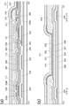
도 1은 본 발명의 일 형태를 설명한 상면도.
도 2a 및 도 2b는 본 발명의 일 형태를 설명한 단면도.
도 3은 본 발명의 일 형태를 설명한 상면도.
도 4는 본 발명의 일 형태를 설명한 단면도.
도 5a 내지 도 5c는 본 발명의 일 형태를 설명한 회로도.
도 6은 본 발명의 일 형태를 설명한 상면도.
도 7은 본 발명의 일 형태를 설명한 상면도.
도 8a 및 도 8b는 본 발명의 일 형태를 설명한 단면도.
도 9는 본 발명의 일 형태를 설명한 단면도.
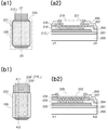
도 10(a1), 도 10(a2), 도 10(b1), 및 도 10(b2)은 본 발명의 일 형태를 설명한 상면도 및 단면도.
도 11(a1), 도 11(a2), 도 11(b1), 도 11(b2), 도 11(c1), 도 11(c2), 도 11(d1), 및 도 11(d2)은 제작 방법을 설명한 도면.
도 12(a1), 도 12(a2), 도 12(b1), 및 도 12(b2)는 제작 방법을 설명한 도면.
도 13(a1), 도 13(a2), 도 13(b1), 도 13(b2), 도 13(c1), 및 도 13(c2)은 제작 방법을 설명한 도면.
도 14a 내지 도 14d는 제작 방법을 설명한 도면.
도 15a 내지 도 15c는 제작 방법을 설명한 도면.
도 16a 내지 도 16c는 본 발명의 일 형태를 설명한 도면.
도 17a 및 도 17b는 본 발명의 일 형태를 설명한 도면.
도 18a 및 도 18b는 본 발명의 일 형태를 설명한 도면.
도 19a 및 도 19b는 본 발명의 일 형태를 설명한 도면.
도 20a 내지 도 20f는 전자 기기를 도시한 도면.1 is a top view illustrating one embodiment of the present invention.
2A and 2B are cross-sectional views illustrating one embodiment of the present invention.
3 is a top view illustrating one embodiment of the present invention.
4 is a cross-sectional view illustrating one embodiment of the present invention.
5A to 5C are circuit diagrams illustrating one embodiment of the present invention.
6 is a top view illustrating one embodiment of the present invention.
7 is a top view illustrating one embodiment of the present invention.
8A and 8B are cross-sectional views illustrating one embodiment of the present invention.
9 is a cross-sectional view illustrating one embodiment of the present invention.
10 (a1), 10 (a2), 10 (b1), and 10 (b2) are top and cross-sectional views illustrating one embodiment of the present invention.
11 (a1), 11 (a2), 11 (b1), 11 (b2), 11 (c1), 11 (c2), 11 (d1), and 11 (d2) are manufactured. Drawings explaining the method.
12 (a1), 12 (a2), 12 (b1), and 12 (b2) are diagrams illustrating a manufacturing method.
13 (a1), 13 (a2), 13 (b1), 13 (b2), 13 (c1), and 13 (c2) are diagrams illustrating a manufacturing method.
14A to 14D are views for explaining the manufacturing method.
15A to 15C are diagrams illustrating a manufacturing method.
16A to 16C illustrate one embodiment of the present invention.
17A and 17B illustrate one embodiment of the present invention.
18A and 18B illustrate one embodiment of the present invention.
19A and 19B illustrate one embodiment of the present invention.
20A-20F illustrate electronic devices.
실시형태에 대하여, 도면을 사용하여 상세하게 설명한다. 다만, 본 발명은 이하의 설명에 한정되지 않고, 본 발명의 취지 및 그 범위에서 벗어남이 없이 그 형태 및 상세를 다양하게 변경할 수 있는 것은 당업자라면 용이하게 이해할 수 있다. 따라서, 본 발명은 이하에 제시되는 실시형태의 기재 내용에 한정하여 해석되는 것은 아니다. 또한, 이하에 설명하는 발명의 구성에 있어서, 동일 부분 또는 같은 기능을 갖는 부분에는 동일한 부호를 다른 도면간에서 공통적으로 사용하고, 그 반복 설명은 생략한다.EMBODIMENT OF THE INVENTION Embodiment is described in detail using drawing. However, the present invention is not limited to the following description, and it can be easily understood by those skilled in the art that various changes can be made in form and detail without departing from the spirit and scope of the present invention. Therefore, this invention is not limited to description of embodiment shown below. In addition, in the structure of the invention demonstrated below, the same code | symbol is used for the same part or the part which has the same function in common between different drawings, and the repeated description is abbreviate | omitted.
또한, 본 명세서 등에서의 "제 1", "제 2", "제 3" 등의 서수는, 구성 요소의 혼동을 피하기 위하여 붙이는 것이며, 수적으로 한정되는 것은 아니다.In addition, ordinal numbers, such as "first", "second", "third", and the like in the present specification and the like are attached to avoid confusion of components, and are not limited in number.
또한, 도면 등에서 제시하는 각 구성의, 위치, 크기, 범위 등은 이해하기 쉽게 하기 위하여 실제의 위치, 크기, 범위 등을 나타내지 않은 경우가 있다. 따라서, 개시하는 발명은 반드시 도면 등에서 개시한 위치, 크기, 범위 등에 한정되지 않는다.In addition, the position, size, range, etc. of each structure shown by drawing etc. may not show actual position, size, range, etc. for easy understanding. Accordingly, the disclosed invention is not necessarily limited to the position, size, range, and the like disclosed in the drawings.
트랜지스터는 반도체 소자의 1종이고, 전류나 전압의 증폭이나 도통 또는 비도통을 제어하는 스위칭 동작 등을 실현할 수 있다. 본 명세서에서의 트랜지스터는 IGFET(Insulated Gate Field Effect Transistor)나 박막 트랜지스터(TFT: Thin Film Transistor)를 포함한다.The transistor is one kind of semiconductor element and can realize a switching operation for controlling amplification, conduction, or non-conduction of a current or voltage. Transistors in the present specification include an IGFET (Insulated Gate Field Effect Transistor) or a thin film transistor (TFT).
또한, 트랜지스터의 "소스"나 "드레인"의 기능은, 다른 극성의 트랜지스터를 채용하는 경우나, 회로 동작에 있어서 전류의 방향이 변화되는 경우 등에 교체되는 경우가 있다. 따라서, 본 명세서에서는 "소스"나 "드레인"이라는 용어는 교체하여 사용할 수 있는 것으로 한다.In addition, the functions of the "source" and "drain" of the transistor may be replaced when a transistor having a different polarity is employed or when the direction of the current changes in a circuit operation. Therefore, in this specification, the terms "source" and "drain" are used interchangeably.
또한, 본 명세서 등에 있어서, "전극"이나 "배선"이라는 용어는 이들 구성 요소를 기능적으로 한정하는 것은 아니다. 예를 들어, "전극"은 "배선"의 일부로서 사용될 수 있고, 또한 그 반대도 마찬가지이다. 또한, "전극"이나 "배선"이라는 용어는 복수의 "전극"이나 "배선"이 일체가 되어 형성되어 있는 경우 등도 포함한다.In addition, in this specification and the like, the terms "electrode" and "wiring" do not functionally limit these components. For example, "electrode" can be used as part of "wiring" and vice versa. The term "electrode" or "wiring" also includes the case where a plurality of "electrodes"
(실시형태 1)(Embodiment 1)
본 실시형태에서는 배선 저항을 저감시킨 반도체 장치의 구성 및 제작 방법의 일례에 대하여 도 1 내지 도 15c를 사용하여 설명한다. 또한 본 실시형태에서는 반도체 장치의 일 형태인 표시 장치에 적용하는 예를 제시한다.In this embodiment, an example of the structure and manufacturing method of the semiconductor device which reduced wiring resistance is demonstrated using FIG. 1 thru | or FIG. 15C. Moreover, in this embodiment, the example applied to the display apparatus which is one form of a semiconductor device is shown.
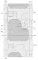
도 5a에, 표시 장치에 사용하는 반도체 장치(100)의 구성예를 도시하였다. 반도체 장치(100)는, 기판(101) 위에 화소 영역(102)과, 단자(107) 및 m개(m은 1 이상의 정수)의 단자(105)를 갖는 단자부(103)와, n개(n은 1 이상의 정수)의 단자(106)를 갖는 단자부(104)를 갖는다. 또한, 반도체 장치(100)는, 단자부(103)에 전기적으로 접속되는 배선(203) 및 m개의 배선(212)과, 단자부(104)에 전기적으로 접속되는 n개의 배선(216)을 갖는다. 또한, 화소 영역(102)은, 세로 m개(행)×가로 n개(열)의 매트릭스 형상으로 배치된 복수의 화소(110)를 갖는다. i행 j열의 화소(110)(i, j)(i는 1 이상 m 이하의 정수이고, j는 1 이상 n 이하의 정수)는 행 방향으로 연장되는 배선(212_i)과 열 방향으로 연장되는 배선(216_j)에 각각 전기적으로 접속된다. 또한, 각 화소는 용량 전극 또는 용량 배선으로서 기능하는 배선(203)과 접속되고, 배선(203)은 단자(107)와 전기적으로 접속된다. 또한, 배선(212_i)은 단자(105_i)와 전기적으로 접속되고, 배선(216_j)은 단자(106_j)와 전기적으로 접속된다.5A illustrates an example of a configuration of a
단자부(103) 및 단자부(104)는 외부 입력 단자이며 외부에 제공된 제어 회로와 FPC(Flexible Printed Circuit) 등을 이용하여 접속된다. 외부에 제공된 제어 회로로부터 공급되는 신호는, 단자부(103) 및 단자부(104)를 통하여 반도체 장치(100)에 입력된다. 도 5a에는, 단자부(103)를 화소 영역(102)의 좌우 외측에 형성하고, 이 2군데에서 신호를 입력하는 구성을 도시하였다. 또한, 단자부(104)를 화소 영역(102)의 상하 외측에 형성하고, 이 2군데에서 신호를 입력하는 구성을 도시하였다. 2군데에서 신호를 입력함으로써 신호의 공급 능력이 높아지기 때문에, 반도체 장치(100)의 고속 동작이 용이해진다. 또한, 반도체 장치(100)의 대형화나 고정세화에 따른 배선 저항의 증대로 인한 신호 지연의 영향을 경감시킬 수 있다. 또한, 반도체 장치(100)에 용장성(redundancy)을 갖게 하는 것이 가능하게 되므로, 반도체 장치(100)의 신뢰성을 향상시킬 수 있다. 또한, 도 5a에서는 단자부(103) 및 단자부(104)를 각각 2군데에 제공하는 구성으로 하였지만, 각각 1군데에 제공하는 구성으로 하여도 좋다.The
반도체 장치(100)를 액정 표시 장치로서 사용하는 경우에 화소(110)로서 사용하는 것이 가능한 회로 구성의 일례를 화소(210)로서 도 5b에 도시하였다. 도 5b에 예시한 화소(210)는, 트랜지스터(111)와, 액정 소자(112)와, 용량 소자(113)를 갖는다. 트랜지스터(111)의 게이트 전극은 배선(212_i)과 전기적으로 접속되고, 트랜지스터(111)의 소스 전극 또는 드레인 전극 중 한쪽은 배선(216_j)과 전기적으로 접속된다. 또한, 트랜지스터(111)의 소스 전극 또는 드레인 전극의 다른 쪽은, 액정 소자(112)의 한쪽의 전극과, 용량 소자(113)의 한쪽의 전극과 전기적으로 접속된다. 액정 소자(112)의 다른 쪽의 전극은, 전극(114)과 전기적으로 접속된다. 전극(114)의 전위는, 0V나, GND나, 공통 전위 등의 고정 전위로 하면 좋다. 용량 소자(113)의 다른 쪽의 전극은, 배선(203)에 전기적으로 접속된다.When the
트랜지스터(111)는 배선(216_j)으로부터 공급되는 화상 신호를 액정 소자(112)에 입력할지 여부를 선택하는 기능을 갖는다. 배선(212_i)에 트랜지스터(111)를 온 상태로 하는 신호가 공급되면, 트랜지스터(111)를 통하여 배선(216_j)으로부터의 화상 신호가 액정 소자(112)에 공급된다. 액정 소자(112)는, 공급되는 화상 신호(전위)에 따라 빛의 투과율이 제어된다. 용량 소자(113)는, 액정 소자(112)에 공급된 전위를 유지하기 위한 유지 용량(Cs 용량이라고도 함)으로서의 기능을 갖는다. 용량 소자(113)를 제공함으로써, 트랜지스터(111)가 오프 상태일 때 소스 전극과 드레인 전극간에 흐르는 전류(오프 전류)에 기인하는, 액정 소자(112)에 공급된 전위의 변동을 억제할 수 있다.The
반도체 장치(100)를 EL 표시 장치로서 사용하는 경우에 화소(110)로서 사용하는 것이 가능한 회로 구성의 일례를 화소(310)로서 도 5c에 도시하였다. 도 5c에 예시한 화소(310)는 트랜지스터(111)와, 트랜지스터(121)와, EL소자(122)와, 용량 소자(113)를 갖는다. 트랜지스터(111)의 게이트 전극은 배선(212_i)과 전기적으로 접속되고, 트랜지스터(111)의 소스 전극 또는 드레인 전극 중 한쪽은 배선(216_j)과 전기적으로 접속된다. 또한, 트랜지스터(111)의 소스 전극 또는 드레인 전극 중 다른 쪽은 트랜지스터(121)의 게이트 전극과 용량 소자(113)의 한쪽의 전극이 전기적으로 접속된 노드(115)와 전기적으로 접속된다. 또한, 트랜지스터(121)의 소스 전극 또는 드레인 전극 중 한쪽은 EL소자(122)의 한쪽의 전극과 전기적으로 접속되고, 소스 전극 또는 드레인 전극 중 다른 쪽은 용량 소자(113)의 다른 쪽의 전극과 배선(203)에 전기적으로 접속된다. 또한, EL소자(122)의 다른 쪽의 전극은 전극(114)과 전기적으로 접속된다. 전극(114)의 전위는, 0V나, GND나, 공통 전위 등의 고정 전위로 하면 좋다. 배선(203)과 전극(114)의 전위차는 트랜지스터(121)의 문턱 전압과 EL소자(122)의 문턱 전압의 합계 전압보다 크게 되도록 설정한다.An example of a circuit configuration that can be used as the
트랜지스터(111)는, 배선(216_j)으로부터 공급되는 화상 신호를 트랜지스터(121)의 게이트 전극에 입력할지 여부를 선택하는 기능을 갖는다. 배선(212_i)에 트랜지스터(111)를 온 상태로 하는 신호가 공급되면, 트랜지스터(111)를 통하여 배선(216_j)으로부터의 화상 신호가 노드(115)에 공급된다.The
트랜지스터(121)는 노드(115)에 공급된 전위(화상 신호)에 따른 전류를 EL소자(122)에 흘리는 기능을 갖는다. 용량 소자(113)는 노드(115)와 배선(203)의 전위차를 일정하게 유지하는 기능을 갖는다. 트랜지스터(121)는 EL소자(122)에 화상 신호에 따른 전류를 흘리기 위한 전류원으로서 기능한다.The
트랜지스터(111)의 채널이 형성되는 반도체층에는 산화물 반도체를 사용할 수 있다. 산화물 반도체는, 에너지갭이 3.0eV 이상으로 크고, 가시광에 대한 투과율이 크다. 또한, 산화물 반도체를 적절한 조건으로 가공하여 얻어진 트랜지스터에서는, 오프 전류 사용시의 온도 조건하(예를 들어, 25℃)에서 100zA(1×10-19A) 이하, 또는 10zA(1×10-20A) 이하, 또는 1zA(1×10-21A) 이하로 할 수 있다. 그러므로, 소비 전력이 적은 반도체 장치를 제공할 수 있다. 또한 반도체층에 산화물 반도체를 사용함으로써 용량 소자(113)를 제공하지 않아도 액정 소자(112)에 인가된 전위의 유지가 가능하게 되므로, 화소의 개구율을 높일 수 있어 표시 품위가 좋고 소비 전력이 저감된 표시 장치를 제공할 수 있다.An oxide semiconductor can be used for the semiconductor layer in which the channel of the
반도체층에 사용하는 산화물 반도체는 수분 또는 수소 등 불순물이 저감되고 산화물 반도체 내의 산소 결손을 저감시킴으로써 i형(진성) 또는 실질적으로 i형화된 산화물 반도체를 사용하는 것이 바람직하다.The oxide semiconductor used for the semiconductor layer preferably uses an i-type (intrinsic) or substantially i-type oxide semiconductor by reducing impurities such as moisture or hydrogen and reducing oxygen vacancies in the oxide semiconductor.
전자 공여체(도너)가 되는 수분 또는 수소 등의 불순물이 저감되어 고순도화된 산화물 반도체(purified OS)는, 그 후 산화물 반도체에 산소를 공급하여 산화물 반도체 내의 산소 결손을 저감시킴으로써 i형(진성)의 산화물 반도체 또는 i형에 매우 가까운(실질적으로 i형화된) 산화물 반도체로 할 수 있다. 채널이 형성되는 반도체층에 i형 또는 실질적으로 i형화된 산화물 반도체를 사용한 트랜지스터는, 오프 전류가 현저히 낮다는 특성을 갖는다. 구체적으로는, 고순도화된 산화물 반도체란, 2차 이온 질량 분석법(SIMS: Secondary Ion Mass Spectrometry)에 의한 수소 농도의 측정값이 5×10¹⁹/cm3 이하, 바람직하게는 5×10¹⁸/cm3 이하, 더 바람직하게는 5×10¹⁷/cm3 이하인 것을 말한다.An oxide semiconductor (purified OS), which is highly purified by reducing impurities such as moisture or hydrogen, which becomes an electron donor (donor), is then supplied with oxygen to the oxide semiconductor to reduce oxygen deficiency in the oxide semiconductor, thereby reducing the i-type (intrinsic) It can be set as an oxide semiconductor or an oxide semiconductor very close to the i-type (substantially i-typed). The transistor using an i-type or substantially i-type oxide semiconductor as the semiconductor layer in which the channel is formed has a characteristic that the off current is significantly low. Specifically, the highly purified oxide semiconductor has a measured value of hydrogen concentration by secondary ion mass spectrometry (SIMS) of 5 × 10 19 / cm 3 or less, preferably 5 × 10 18 / cm 3 or less, More preferably, it is 5 * 10 <17> / cm <3> or less.
또한, 홀 효과 측정에 의하여 측정할 수 있는, i형 또는 실질적으로 i형화된 산화물 반도체의 캐리어 밀도는 1×10¹⁴/cm3 미만, 바람직하게는 1×10¹²/cm3 미만, 더 바람직하게는 1×10¹¹/cm3 미만이다. 또한, 산화물 반도체의 밴드갭은 2eV 이상, 바람직하게는 2.5eV 이상, 더 바람직하게는 3eV 이상이다. 채널이 형성되는 반도체층에 i형 또는 실질적으로 i형화된 산화물 반도체를 사용함으로써, 트랜지스터의 오프 전류를 저감시킬 수 있다.Further, the carrier density of the i-type or substantially i-typed oxide semiconductor, which can be measured by Hall effect measurement, is less than 1 × 10 14 / cm 3 , preferably less than 1 × 10 12 / cm 3 , more preferably Is less than 1 × 10 11 / cm 3 . The band gap of the oxide semiconductor is 2 eV or more, preferably 2.5 eV or more, more preferably 3 eV or more. By using an i-type or substantially i-type oxide semiconductor in the semiconductor layer in which the channel is formed, the off current of the transistor can be reduced.
여기서, 산화물 반도체 내의 수소 농도의 SIMS 분석에 대하여 설명하기로 한다. SIMS 분석은, 그 원리상 시료 표면 근방이나, 재질이 상이한 막과의 적층 계면 근방의 데이터를 정확하게 얻기가 어렵다는 것이 알려져 있다. 그래서, 막 내에 있어서의 수소 농도의 두께 방향의 분포를 SIMS로 분석하는 경우, 대상이 되는 막이 존재하는 범위에 있어서, 값이 극단적으로 변동되는 일이 없고 거의 일정한 값이 얻어지는 영역에서의 평균값을 수소 농도로서 채용한다. 또한, 측정의 대상이 되는 막의 두께가 작은 경우, 인접하는 막 내의 수소 농도의 영향을 받아 거의 일정한 값이 얻어지는 영역을 찾을 수 없는 경우가 있다. 이 경우, 상기 막이 존재하는 영역에 있어서의, 수소 농도의 최대값 또는 최소값을 상기 막 내의 수소 농도로서 채용한다. 또한, 상기 막이 존재하는 영역에 있어서, 최대값을 갖는 산 형상의 피크, 최소값을 갖는 골짜기 형상의 피크가 존재하지 않은 경우, 변곡점의 값을 수소 농도로서 채용한다.Here, SIMS analysis of the hydrogen concentration in the oxide semiconductor will be described. It is known that SIMS analysis is difficult to accurately obtain data in the vicinity of the sample surface and in the vicinity of the laminated interface with the film having different materials. Therefore, when analyzing the distribution of the thickness direction of the hydrogen concentration in a film | membrane by SIMS, the average value in the area | region where a value does not fluctuate extremely and an almost constant value is obtained in the range in which the target film exists is hydrogen. It is adopted as a concentration. In addition, when the thickness of the film to be measured is small, there is a case where an area where an almost constant value is obtained may not be found under the influence of the hydrogen concentration in the adjacent film. In this case, the maximum or minimum value of the hydrogen concentration in the region where the film is present is employed as the hydrogen concentration in the film. In the region where the film is present, when the peak in the form of an acid having a maximum value and the valley peak having a minimum value do not exist, the value of the inflection point is employed as the hydrogen concentration.
채널이 형성되는 반도체층에 사용하는 산화물 반도체로서는, 적어도 인듐(In) 또는 아연(Zn)을 포함하는 것이 바람직하다. 특히 In과 Zn을 양쪽 모두 포함하는 것이 바람직하다. 또한, 상기 산화물 반도체를 사용한 트랜지스터의 전기 특성의 불균일을 감소시키기 위한 스테빌라이저로서, 이들에 더하여 갈륨(Ga)을 갖는 것이 바람직하다. 또한, 스테빌라이저로서 주석(Sn)을 갖는 것이 바람직하다. 또한, 스테빌라이저로서 하프늄(Hf)을 갖는 것이 바람직하다. 또한, 스테빌라이저로서 알루미늄(Al)을 갖는 것이 바람직하다.As an oxide semiconductor used for the semiconductor layer in which a channel is formed, it is preferable to contain at least indium (In) or zinc (Zn). It is particularly preferable to include both In and Zn. Moreover, as a stabilizer for reducing the nonuniformity of the electrical characteristics of the transistor using the said oxide semiconductor, it is preferable to have gallium (Ga) in addition to these. Further, it is preferable to have tin (Sn) as a stabilizer. Further, it is preferable to have hafnium (Hf) as a stabilizer. Further, it is preferable to have aluminum (Al) as a stabilizer.
또한, 다른 스테빌라이저로서, 란타노이드인, 란탄(La), 세륨(Ce), 프라세오디뮴(Pr), 네오디뮴(Nd), 사마륨(Sm), 유로퓸(Eu), 가돌리늄(Gd), 테르븀(Tb), 디스프로슘(Dy), 홀뮴(Ho), 에르븀(Er), 툴륨(Tm), 이테르븀(Yb), 루테튬(Lu) 중 어느 1종 또는 복수종을 가져도 좋다.In addition, as other stabilizers, lanthanoids, lanthanum (La), cerium (Ce), praseodymium (Pr), neodymium (Nd), samarium (Sm), europium (Eu), gadolinium (Gd), terbium (Tb) Or any one or more of dysprosium (Dy), holmium (Ho), erbium (Er), thulium (Tm), ytterbium (Yb), and lutetium (Lu).
예를 들면, 산화물 반도체로서, 산화 인듐, 산화 주석, 산화 아연, 2원계 금속의 산화물인 In-Zn계 산화물, Sn-Zn계 산화물, Al-Zn계 산화물, Zn-Mg계 산화물, Sn-Mg계 산화물, In-Mg계 산화물, In-Ga계 산화물, 3원계 금속의 산화물인 In-Ga-Zn계 산화물(IGZO라고도 표기함), In-Al-Zn계 산화물, In-Sn-Zn계 산화물, Sn-Ga-Zn계 산화물, Al-Ga-Zn계 산화물, Sn-Al-Zn계 산화물, In-Hf-Zn계 산화물, In-La-Zn계 산화물, In-Ce-Zn계 산화물, In-Pr-Zn계 산화물, In-Nd-Zn계 산화물, In-Sm-Zn계 산화물, In-Eu-Zn계 산화물, In-Gd-Zn계 산화물, In-Tb-Zn계 산화물, In-Dy-Zn계 산화물, In-Ho-Zn계 산화물, In-Er-Zn계 산화물, In-Tm-Zn계 산화물, In-Yb-Zn계 산화물, In-Lu-Zn계 산화물, 4원계 금속의 산화물인 In-Sn-Ga-Zn계 산화물, In-Hf-Ga-Zn계 산화물, In-Al-Ga-Zn계 산화물, In-Sn-Al-Zn계 산화물, In-Sn-Hf-Zn계 산화물, In-Hf-Al-Zn계 산화물을 사용할 수 있다. 또한, 상기 산화물 반도체에 SiO2를 포함시켜도 좋다.For example, indium oxide, tin oxide, zinc oxide, In-Zn oxide, Sn-Zn oxide, Al-Zn oxide, Zn-Mg oxide, Sn-Mg which are oxides of binary metals as oxide semiconductors Oxides, In-Mg oxides, In-Ga oxides, In-Ga-Zn oxides (also referred to as IGZO), oxides of ternary metals, In-Al-Zn oxides, In-Sn-Zn oxides , Sn-Ga-Zn oxide, Al-Ga-Zn oxide, Sn-Al-Zn oxide, In-Hf-Zn oxide, In-La-Zn oxide, In-Ce-Zn oxide, In -Pr-Zn oxide, In-Nd-Zn oxide, In-Sm-Zn oxide, In-Eu-Zn oxide, In-Gd-Zn oxide, In-Tb-Zn oxide, In-Dy -Zn oxide, In-Ho-Zn oxide, In-Er-Zn oxide, In-Tm-Zn oxide, In-Yb-Zn oxide, In-Lu-Zn oxide, quaternary metal oxide Phosphorus In-Sn-Ga-Zn-based oxide, In-Hf-Ga-Zn-based oxide, In-Al-Ga-Zn-based oxide, In-Sn-Al-Zn-based oxide, In-Sn-Hf-Zn-based oxide , In-Hf-Al-Zn-based oxides can be used have. Further, SiO 2 may be included in the oxide semiconductor.
여기서, 예를 들면 In-Ga-Zn계 산화물이란, 인듐(In), 갈륨(Ga), 아연(Zn)을 갖는 산화물이라는 뜻이고 In과 Ga와 Zn의 비율은 불문한다. 또한, In과 Ga와 Zn 이외의 금속 원소를 포함해도 된다. 이때, 산화물 반도체의 화학 양론비에 대하여 산소를 과잉으로 하면 바람직하다. 산소를 과잉으로 함으로써 산화물 반도체의 산소 결손에 기인하는 캐리어의 생성을 억제할 수 있다.Here, for example, an In—Ga—Zn-based oxide means an oxide having indium (In), gallium (Ga), and zinc (Zn), and the ratio of In, Ga, and Zn is irrelevant. Moreover, metal elements other than In, Ga, and Zn may be included. At this time, it is preferable to make oxygen excess with respect to the stoichiometric ratio of an oxide semiconductor. By making oxygen excess, generation | occurrence | production of the carrier resulting from the oxygen deficiency of an oxide semiconductor can be suppressed.
또한, 산화물 반도체층은, 화학식 InMO3(ZnO)m(m>0)로 표기되는 박막을 사용할 수 있다. 여기서, M은 Sn, Zn, Ga, Al, Mn 및 Co 중에서 선택된 하나의 금속 원소 또는 복수의 금속 원소를 나타낸다. 또한, 산화물 반도체층으로서, In2SnO5(ZnO)n(n>0)으로 표기되는 재료를 사용하여도 좋다.As the oxide semiconductor layer, a thin film represented by the formula InMO 3 (ZnO) m (m> 0) can be used. Here, M represents one metal element or a plurality of metal elements selected from Sn, Zn, Ga, Al, Mn, and Co. As the oxide semiconductor layer, a material represented by In 2 SnO 5 (ZnO) n (n> 0) may be used.
예를 들어, 원자수비가 In: Ga: Zn=1: 1: 1(=1/3: 1/3: 1/3) 또는 In: Ga: Zn=2: 2: 1(=2/5: 2/5: 1/5)인 In-Ga-Zn계 산화물이나 그 조성의 근방의 산화물을 사용할 수 있다. 또는, 원자수비가 In: Sn: Zn=1: 1: 1(=1/3: 1/3: 1/3), In: Sn: Zn=2: 1: 3(=1/3: 1/6: 1/2) 또는 In: Sn: Zn=2: 1: 5(=1/4: 1/8: 5/8)인 In-Sn-Zn계 산화물이나 그 조성의 근방의 산화물을 사용하면 좋다.For example, the atomic ratio is In: Ga: Zn = 1: 1: 1 (= 1/3: 1/3: 1/3) or In: Ga: Zn = 2: 2: 1 (= 2/5: 2/5: 1/5) In-Ga-Zn type oxide and the oxide of the composition vicinity can be used. Alternatively, the atomic ratio is In: Sn: Zn = 1: 1: 1 (= 1/3: 1/3: 1/3), In: Sn: Zn = 2: 1: 3 (= 1/3: 1 / 6: 1/2) or In: Sn: Zn = 2: 1: 5 (= 1/4: 1/8: 5/8) In-Sn-Zn-based oxide or an oxide in the vicinity of the composition good.
그러나, 이들에 한정되지 않으며, 필요로 하는 반도체 특성(이동도, 문턱값, 편차 등)에 따라 적절한 조성의 것을 사용하면 좋다. 또한, 필요로 하는 반도체 특성을 얻기 위하여, 캐리어 농도나 불순물 농도, 결함 밀도, 금속 원소와 산소의 원자수비, 원자간 거리, 밀도 등을 적절한 것으로 하는 것이 바람직하다.However, it is not limited to these, What is necessary is just to use the thing of a suitable composition according to the semiconductor characteristic (mobility, a threshold value, a deviation, etc.) required. Moreover, in order to acquire the required semiconductor characteristic, it is preferable to make carrier density | concentration, impurity concentration, defect density, atomic ratio of a metal element and oxygen, interatomic distance, density, etc. suitable.
예를 들어, In-Sn-Zn계 산화물은 비교적 용이하게 높은 이동도를 얻을 수 있다. 그러나, In-Ga-Zn계 산화물을 사용한 경우에도 벌크 내의 결함 밀도를 저감시킴으로써 이동도를 높일 수 있다.For example, In—Sn—Zn-based oxides can obtain high mobility relatively easily. However, even when In-Ga-Zn-based oxides are used, mobility can be increased by reducing the defect density in the bulk.
또한, 예를 들면, In, Ga, Zn의 원자수비가 In: Ga: Zn=a: b: c(a+b+c=1)인 산화물과 원자수비가 In: Ga: Zn=A: B: C(A+B+C=1)인 산화물의 조성이 근방이라는 것은, a, b, c가, (a-A)2+(b-B)2+(c-C)2≤r2를 만족시키는 것을 말하며, r은 예를 들면 0.05로 하면 좋다. 다른 산화물도 마찬가지이다.Further, for example, an oxide having an atomic ratio of In, Ga, and Zn is In: Ga: Zn = a: b: c (a + b + c = 1) and an atomic ratio of In: Ga: Zn = A: B : The composition of the oxide of C (A + B + C = 1) in the vicinity means that a, b, and c satisfy (aA) 2 + (bB) 2 + (cC) 2 ≤ r 2 , r may be 0.05, for example. The same applies to other oxides.
산화물 반도체층은 단결정이라도 좋고, 비단결정이라도 좋다. 후자의 경우 비정질이라도 다결정(폴리크리스탈이라고도 함)이라도 좋다. 또한, 비정질 내에 결정성을 갖는 부분을 포함하는 구조라도 좋다.The oxide semiconductor layer may be a single crystal or a non-single crystal. In the latter case, it may be amorphous or polycrystalline (also called polycrystal). Moreover, the structure containing the part which has crystallinity in amorphous may be sufficient.
비정질(어모퍼스) 상태의 산화물 반도체는, 비교적 용이하게 평탄한 표면을 얻을 수 있기 때문에, 이것을 사용하여 트랜지스터를 제작하였을 때의 계면 산란을 저감시킬 수 있어, 비교적 용이하게, 비교적 높은 이동도를 얻을 수 있다.Since the oxide semiconductor in the amorphous (amorphous) state can obtain a flat surface relatively easily, the interfacial scattering when a transistor is fabricated using this can be reduced, and relatively high mobility can be obtained relatively easily. .
또한, 산화물 반도체로서 In-Zn계 산화물의 재료를 사용하는 경우, 원자수비로, In/Zn=0.5 이상 50 이하, 바람직하게는 In/Zn=1 이상 20 이하, 더욱 바람직하게는 In/Zn=1.5 이상 15 이하로 한다. Zn의 원자수비를 바람직한 상기 범위로 함으로써, 트랜지스터의 전계 효과 이동도를 향상시킬 수 있다. 여기서, 화합물의 원자수비가 In: Zn: O=X: Y: Z일 때 Z>1.5X+Y로 한다.In the case of using an In—Zn-based oxide material as the oxide semiconductor, in atomic ratio, In / Zn = 0.5 or more and 50 or less, preferably In / Zn = 1 or more and 20 or less, more preferably In / Zn = It is 1.5 or more and 15 or less. By setting the atomic ratio of Zn to the above preferable range, the field effect mobility of the transistor can be improved. Here, when the atomic number ratio of the compound is In: Zn: O = X: Y: Z, let Z> 1.5X + Y.
산화물 반도체층은, 예를 들어 비단결정을 가져도 좋다. 비단결정은 예를 들어 CAAC(C Axis Aligned Crystal), 다결정, 미결정, 비정질부를 갖는다. 비정질부는, 미결정, CAAC보다 결함 준위 밀도가 높다. 또한, 미결정은 CAAC보다 결함 준위 밀도가 높다. 또한, CAAC를 갖는 산화물 반도체를 CAAC-OS(C Axis Aligned Crystalline Oxide Semiconductor)라고 부른다.The oxide semiconductor layer may have, for example, a non-single crystal. The non-single crystal has, for example, CAAC (C Axis Aligned Crystal), polycrystalline, microcrystalline, amorphous part. The amorphous portion has a higher density of defect states than microcrystalline or CAAC. In addition, microcrystalline has a higher defect level density than CAAC. Further, an oxide semiconductor having CAAC is called CAAC-OS (C Axis Aligned Crystalline Oxide Semiconductor).
산화물 반도체층은, 예를 들어 CAAC-OS를 가져도 좋다. CAAC-OS는 예를 들어 c축 배향하고, a축 또는/및 b축은 거시적으로 보면 정렬되어 있지 않다.The oxide semiconductor layer may have a CAAC-OS, for example. The CAAC-OS is for example c-axis oriented and the a-axis and / or b-axis are not aligned macroscopically.
산화물 반도체층은 예를 들어 미결정을 가져도 좋다. 또한, 미결정을 갖는 산화물 반도체를 미결정 산화물 반도체라고 부른다. 미결정 산화물 반도체층은 예를 들어 1nm 이상 10nm 미만의 사이즈의 미결정(나노 결정이라고도 함)을 막 내에 포함하는 산화물 반도체를 갖는다. 또는 미결정 산화물 반도체층은 예를 들어 1nm 이상 10nm 미만의 결정부를 갖는 결정-비정질 혼상 구조의 산화물 반도체를 갖는다.The oxide semiconductor layer may have microcrystals, for example. Further, the oxide semiconductor having microcrystalline is called a microcrystalline oxide semiconductor. The microcrystalline oxide semiconductor layer has, for example, an oxide semiconductor containing microcrystals (also referred to as nanocrystals) having a size of 1 nm or more and less than 10 nm. Or the microcrystalline oxide semiconductor layer has, for example, an oxide semiconductor having a crystal-amorphous mixed phase structure having a crystal portion of 1 nm or more and less than 10 nm.
산화물 반도체층은 예를 들어 비정질부를 가져도 좋다. 또한, 비정질부를 갖는 산화물 반도체를 비정질 산화물 반도체라고 부른다. 비정질 산화물 반도체층은 예를 들어 원자 배열이 무질서한 층이고, 결정 성분을 갖지 않는다. 또는 비정질 산화물 반도체층은 예를 들어 완전한 비정질이고, 결정부를 갖지 않는다.The oxide semiconductor layer may have an amorphous portion, for example. Further, an oxide semiconductor having an amorphous portion is called an amorphous oxide semiconductor. The amorphous oxide semiconductor layer is, for example, a disordered atomic array and has no crystal component. Or the amorphous oxide semiconductor layer is, for example, completely amorphous and has no crystal.
또한, 산화물 반도체층이 CAAC-OS, 미결정 산화물 반도체, 비정질 산화물 반도체의 혼합층이어도 좋다. 혼합층은 예를 들어 비정질 산화물 반도체의 영역과, 미결정 산화물 반도체의 영역과, CAAC-OS의 영역을 갖는다. 또한, 혼합층은 예를 들어 비정질 산화물 반도체의 영역과, 미결정 산화물 반도체의 영역과, CAAC-OS의 영역의 적층 구조를 가져도 좋다.The oxide semiconductor layer may be a mixed layer of CAAC-OS, microcrystalline oxide semiconductor, and amorphous oxide semiconductor. The mixed layer has, for example, a region of an amorphous oxide semiconductor, a region of a microcrystalline oxide semiconductor, and a region of CAAC-OS. In addition, the mixed layer may have a laminated structure of, for example, a region of an amorphous oxide semiconductor, a region of a microcrystalline oxide semiconductor, and a region of a CAAC-OS.
또한, 산화물 반도체층은 예를 들어 단결정을 가져도 좋다.In addition, the oxide semiconductor layer may have, for example, a single crystal.
산화물 반도체층은 복수의 결정부를 갖고, 상기 결정부의 c축이 피형성면의 법선 벡터 또는 표면의 법선 벡터에 평행한 방향으로 정렬되어 있는 것이 바람직하다. 또한, 상이한 결정부들 사이에서 a축 및 b축의 방향이 각각 상이하여도 좋다. 이와 같은 산화물 반도체층의 일례로서는, CAAC-OS층이 있다.The oxide semiconductor layer has a plurality of crystal parts, and the c axis of the crystal parts is preferably aligned in a direction parallel to the normal vector of the surface to be formed or the normal vector of the surface. In addition, the directions of the a-axis and the b-axis may be different between the different crystal parts. An example of such an oxide semiconductor layer is a CAAC-OS layer.
CAAC-OS층은, 완전한 비정질이 아니다. CAAC-OS층은, 예를 들어, 결정부 및 비정질부를 갖는 결정-비정질 혼상 구조의 산화물 반도체를 갖는다. 또한, 상기 결정부는 하나의 변이 100nm 미만의 입방체 내에 들어가는 크기인 경우가 많다. 또한, 투과형 전자 현미경(TEM: Transmission Electron Microscope)에 의한 관찰상에서는 CAAC-OS층에 포함되는 비정질부와 결정부의 경계, 결정부와 결정부의 경계는 명확하지 않다. 또한, TEM에 의하여 CAAC-OS층에 명확한 입계(그레인 바운더리라고도 함)는 확인되지 않는다. 그래서, CAAC-OS층은 입계에 기인하는 전자 이동도의 저하가 억제된다.The CAAC-OS layer is not completely amorphous. The CAAC-OS layer has an oxide semiconductor of a crystal-amorphous mixed phase structure having, for example, a crystal portion and an amorphous portion. In addition, the crystal part often has a size in which one side enters a cube of less than 100 nm. In addition, in the observation by a transmission electron microscope (TEM), the boundary between the amorphous part and the crystal part and the boundary between the crystal part and the crystal part included in the CAAC-OS layer are not clear. In addition, no clear grain boundaries (also called grain boundaries) are identified in the CAAC-OS layer by the TEM. Therefore, in the CAAC-OS layer, the decrease in electron mobility due to grain boundaries is suppressed.
CAAC-OS층에 포함되는 결정부는, 예를 들어 c축이 CAAC-OS층의 피형성면의 법선 벡터 또는 표면의 법선 벡터에 평행한 방향으로 정렬되고, 또 ab면에 수직인 방향에서 볼 때 금속 원자가 삼각형상 또는 육각형상으로 배열하며, c축에 수직인 방향에서 볼 때 금속 원자가 층상 또는 금속 원자와 산소 원자가 층상으로 배열되어 있다. 또한, 상이한 결정부들 사이에서 a축 및 b축의 방향이 각각 상이하여도 좋다. 본 명세서에 있어서, 단순히 수직이라고 기재한 경우, 80° 이상 100° 이하의 범위, 바람직하게는 85° 이상 95° 이하의 범위도 포함되는 것으로 한다. 또한, 단순히 평행이라고 기재한 경우에는 -10° 이상 10° 이하의 범위, 바람직하게는 -5° 이상 5° 이하의 범위도 포함되는 것으로 한다.The crystal part included in the CAAC-OS layer is, for example, when the c-axis is aligned in a direction parallel to the normal vector of the formation surface of the CAAC-OS layer or the normal vector of the surface, and viewed in a direction perpendicular to the ab plane. The metal atoms are arranged in a triangular or hexagonal shape, and the metal atoms are layered or the metal atoms and oxygen atoms are arranged in layers when viewed in a direction perpendicular to the c-axis. In addition, the directions of the a-axis and the b-axis may be different between the different crystal parts. In the present specification, when simply described as vertical, the range of 80 ° or more and 100 ° or less, preferably 85 ° or more and 95 ° or less is also included. In addition, when it describes simply as parallel, the range of -10 degrees or more and 10 degrees or less, Preferably the range of -5 degrees or more and 5 degrees or less shall also be included.
또한, CAAC-OS층에 있어서 결정부의 분포가 균일하지 않아도 좋다. 예를 들어, CAAC-OS층의 형성 과정에서 산화물 반도체층의 표면 측으로부터 결정 성장시키는 경우에는, 피형성면 근방보다 표면 근방에서 결정부가 차지하는 비율이 높은 경우가 있다. 또한, CAAC-OS층에 불순물을 첨가함으로써 상기 불순물 첨가 영역에서 결정부가 비정질화되는 경우도 있다.In addition, the distribution of crystal parts in the CAAC-OS layer may not be uniform. For example, when crystal growth is carried out from the surface side of the oxide semiconductor layer in the process of forming the CAAC-OS layer, the proportion of the crystal portion in the surface vicinity is higher than in the vicinity of the formed surface. In addition, by adding an impurity to the CAAC-OS layer, a crystal part may be amorphous in the impurity addition region.
CAAC-OS층에 포함되는 결정부의 c축은, CAAC-OS층의 피형성면의 법선 벡터 또는 표면의 법선 벡터에 평행한 방향으로 정렬되기 때문에, CAAC-OS층의 형상(피형성면의 단면 형상 또는 표면의 단면 형상)에 따라서는 서로 다른 방향을 향하는 경우가 있다. 또한 결정부는, 성막을 수행하였을 때 또는 성막을 수행한 후에 가열 처리 등의 결정화 처리를 수행하였을 때 형성된다. 따라서, 결정부의 c축은, CAAC-OS층이 형성되었을 때의 피형성면의 법선 벡터 또는 표면의 법선 벡터에 평행한 방향으로 정렬된다.Since the c-axis of the crystal part included in the CAAC-OS layer is aligned in a direction parallel to the normal vector of the surface to be formed of the CAAC-OS layer or the normal vector of the surface, the shape of the CAAC-OS layer (the cross-sectional shape of the surface to be formed) Or the cross-sectional shape of the surface) may face different directions. Further, the crystal part is formed when the film formation is performed or when the crystallization treatment such as heat treatment is performed after the film formation is performed. Therefore, the c-axis of the crystal part is aligned in a direction parallel to the normal vector of the surface to be formed or the normal vector of the surface when the CAAC-OS layer is formed.
CAAC-OS를 사용한 트랜지스터는 가시광이나 자외광의 조사에 기인한 전기 특성의 변동이 작다. 따라서 상기 트랜지스터는 신뢰성이 높다.Transistors using CAAC-OS have a small variation in electrical characteristics due to irradiation of visible or ultraviolet light. Thus, the transistor is highly reliable.
또한 산화물 반도체층을 CAAC-OS로 하기 위해서는, 산화물 반도체층이 형성되는 표면이 비정질이면 바람직하다. 산화물 반도체층이 형성되는 표면이 결정질이면 산화물 반도체층의 결정성이 흩어지기 쉽고 CAAC-OS가 형성되기 어렵다.In addition, in order to make an oxide semiconductor layer into CAAC-OS, it is preferable that the surface on which an oxide semiconductor layer is formed is amorphous. If the surface on which the oxide semiconductor layer is formed is crystalline, crystallinity of the oxide semiconductor layer is easily dispersed, and CAAC-OS is difficult to be formed.
다만 산화물 반도체층이 형성되는 표면은 CAAC 구조를 가져도 좋다. 산화물 반도체층이 형성되는 표면이 CAAC 구조를 갖는 경우에는 산화물 반도체층도 CAAC-OS가 되기 쉽다.However, the surface on which the oxide semiconductor layer is formed may have a CAAC structure. When the surface on which the oxide semiconductor layer is formed has a CAAC structure, the oxide semiconductor layer also tends to be CAAC-OS.
따라서 산화물 반도체층을 CAAC-OS로 하기 위해서는 산화물 반도체층이 형성되는 표면이 비정질이나 CAAC 구조를 가지면 바람직하다.Therefore, to make the oxide semiconductor layer CAAC-OS, it is preferable that the surface on which the oxide semiconductor layer is formed has an amorphous or CAAC structure.
또한 산화물 반도체를 구성하는 산소의 일부는 질소로 치환되어도 좋다.In addition, part of the oxygen constituting the oxide semiconductor may be replaced with nitrogen.
또한, CAAC-OS와 같이 결정부를 갖는 산화물 반도체에서는, 벌크 내의 결함을 더욱 저감시킬 수 있고, 표면의 평탄성을 높이면 비정질 상태의 산화물 반도체 이상의 이동도를 얻을 수 있다. 표면의 평탄성을 높이기 위해서는 평탄한 표면 위에 산화물 반도체를 형성하는 것이 바람직하고, 구체적으로는 평균 면 거칠기(Ra)가 1nm 이하, 바람직하게는 0.3nm 이하, 더 바람직하게는 0.1nm 이하의 표면 위에 형성하면 좋다. Ra는 원자간력 현미경(AFM: Atomic Force Microscope)으로 평가 가능하다.In addition, in oxide semiconductors having crystal parts such as CAAC-OS, defects in the bulk can be further reduced, and the mobility of the oxide semiconductor in an amorphous state can be obtained by increasing the flatness of the surface. In order to increase the flatness of the surface, it is preferable to form an oxide semiconductor on the flat surface. Specifically, when the average surface roughness Ra is formed on the surface of 1 nm or less, preferably 0.3 nm or less, more preferably 0.1 nm or less good. Ra can be evaluated by atomic force microscopy (AFM).
다만, 본 실시형태에서 설명하는 트랜지스터는 보텀 게이트형이므로 산화물 반도체막의 아래 쪽에는 게이트 전극(202)과, 게이트 절연층으로서 기능하는 절연층(204)이 존재한다. 따라서, 상기 평탄한 표면을 얻기 위하여 기판 위에 게이트 전극(202) 및 절연층(204)을 형성한 후, 적어도 게이트 전극(202)과 중첩되는 절연층(204)의 표면에 대하여 화학적 기계 연마(CMP: Chemical Mechanical Polishing) 처리 등의 평탄화 처리를 수행하여도 좋다.However, since the transistor described in this embodiment is a bottom gate type, there is a
산화물 반도체층(205)의 두께는, 1nm 이상 30nm 이하(바람직하게는 5nm 이상 10nm 이하)로 하여, 스퍼터링법, MBE(Molecular Beam Epitaxy)법, CVD법, 펄스 레이저 퇴적법, ALD(Atomic Layer Deposition)법 등을 적절히 이용할 수 있다. 또한 산화물 반도체층(205)은 스퍼터링 타깃 표면에 대하여 대략 수직으로 복수의 기판 표면이 세트된 상태에서 성막을 수행하는 스퍼터링 장치를 사용하여, 형성하여도 좋다.The thickness of the
또한 본 실시형태에서는 트랜지스터를 n채널형의 트랜지스터로서 설명한다.In this embodiment, the transistor is described as an n-channel transistor.
다음에 도 5a에 도시한 화소(110)의 구성예에 대하여 도 1 내지 도 2b를 사용하여 설명한다. 도 1은 도 5a에 도시한 화소(110)의 평면 구성을 설명하는 상면도이고, 도 2a 및 도 2b는 도 5a에 도시한 화소(110)의 적층 구성을 도시한 단면도이다. 또한 도 1에서의 A1-A2, 및 B1-B2의 쇄선은 도 2a 및 도 2b에서의 단면 A1-A2, 단면 B1-B2에 상당한다. 또한 도면을 보기 쉽게 하기 위하여 도 1에서는 일부의 구성 요소의 기재를 생략하였다.Next, a configuration example of the
도 1에 도시한 트랜지스터(111)는, 드레인 전극(206b)을 U자형(C자형, ㄷ자형, 또는 말굽형)의 소스 전극(206a)으로 둘러싸는 형상으로 한 것이다. 이런 형상으로 함으로써, 트랜지스터의 면적이 작아도 충분한 채널 폭을 확보하는 것이 가능하게 되고, 트랜지스터의 도통시에 흐르는 전류(온 전류라고도 함)의 양을 늘리는 것이 가능하게 된다.The
또한, 화소 전극(211)과 전기적으로 접속되는 드레인 전극(206b)과 게이트 전극(202)간에 발생하는 기생 용량이, 소스 전극(206a)과 게이트 전극(202)간에 발생하는 기생 용량보다 크면, 피드스루(feedthrough)의 영향을 받기 쉬워지기 때문에, 액정 소자(112)에 공급된 전위를 정확하게 유지할 수 없어 표시 품위가 저하되는 요인이 된다. 본 실시형태에 나타내는 바와 같이, 소스 전극(206a)을 U자형으로 하여 드레인 전극(206b)을 둘러싸는 형상으로 함으로써, 충분한 채널 폭을 확보하면서, 드레인 전극(206b)과 게이트 전극(202)간에 발생하는 기생 용량을 작게 할 수 있기 때문에, 표시 장치의 표시 품위를 향상시킬 수 있다. 또한 게이트 전극(202)은 배선(212_i)과 접속되고, 소스 전극(206a)은 배선(236)과 접속된다. 또한 도 1 내지 도 2b에는 배선(216_j)은 배선(236)과 배선(226)을 갖고, 배선(236)과 배선(226)을 전기적으로 직렬로 접속하는 예를 도시하였다.In addition, when the parasitic capacitance generated between the
도 2a에 도시한 단면 A1-A2는, 트랜지스터(111) 및 용량 소자(113)의 적층 구조를 나타내었다. 트랜지스터(111)는 채널 에칭형이라고 불리는 보텀 게이트 구조의 트랜지스터이다.Cross sections A1-A2 shown in FIG. 2A show the stacked structure of the
도 2a에 도시한 단면 A1-A2에 있어서, 기판(200) 위에 절연층(201)이 형성되고, 절연층(201) 위에 게이트 전극(202) 및 배선(203)이 형성된다. 또한, 게이트 전극(202) 및 배선(203) 위에, 절연층(204)과 산화물 반도체층(205)이 형성된다. 또한, 산화물 반도체층(205) 위에 소스 전극(206a) 및 드레인 전극(206b)이 형성된다. 또한, 산화물 반도체층(205)의 일부와 접하여 소스 전극(206a) 및 드레인 전극(206b) 위에 절연층(207)이 형성되고, 절연층(207) 위에 절연층(208)이 형성된다. 절연층(208) 위에는 화소 전극(211)이 형성되고, 절연층(207) 및 절연층(208)에 형성된 콘택트 홀(209)을 통하여 드레인 전극(206b)과 전기적으로 접속된다.In cross section A1-A2 shown in FIG. 2A, an insulating
게이트 전극(202), 배선(212_i), 배선(203), 및 배선(226)은 동일한 도전층을 사용하여 형성할 수 있다. 또한 게이트 전극(202), 배선(212_i), 배선(203), 배선(226)을 구리(Cu)를 포함한 도전 재료로 형성함으로써 배선 저항의 증가를 방지할 수 있다. 또한 게이트 전극(202), 배선(212_i), 배선(203), 배선(226)을, Cu를 포함한 도전층과, 텅스텐(W), 탄탈(Ta), 몰리브덴(Mo), 티타늄(Ti), 크롬(Cr) 등의 Cu보다 융점이 높은 금속 원소를 포함한 도전층이나, 상술한 금속 원소의 질화물이나 산화물을 적층함으로써 마이그레이션을 억제하여 반도체 장치의 신뢰성을 향상시킬 수 있다. 예를 들어 질화 탄탈과 구리의 적층으로 한다.The
절연층(204)은 Cu의 확산을 막기 위한 배리어성을 갖는 재료를 사용하여 형성하는 것이 바람직하다. 배리어성을 갖는 재료로서는 예를 들어 질화 실리콘이나 산화 알루미늄을 들 수 있다. Cu를 포함한 배선을, 배리어성을 갖는 절연층으로 덮음으로써 Cu의 확산을 억제할 수 있다.The insulating
또한 산화물 반도체층(205)과 접하여 형성되는 소스 전극(206a) 및 드레인 전극(206b)(이들과 동일한 층으로 형성되는 배선을 포함함)은 Cu를 사용하지 않고 형성하는 것이 바람직하다. 산화물 반도체층(205)과 접하여 형성되는 소스 전극(206a) 및 드레인 전극(206b)에 Cu를 사용하면 소스 전극(206a) 및 드레인 전극(206b) 형성시에 에칭된 Cu가 산화물 반도체층(205) 내에 확산되어 트랜지스터의 전기 특성이나 신뢰성을 열화시키는 원인이 된다. 또한 소스 전극(206a) 및 드레인 전극(206b)은 단층 구조이어도 좋고 복수 층의 적층 구조로 하여도 좋다. 예를 들어 텅스텐과 알루미늄과 티타늄의 3층 구조로 하여도 좋다.In addition, the
또한 배선(203)과 드레인 전극(206b)이 절연층(204)을 개재(介在)하여 중첩되어 있는 부분이, 용량 소자(113)로서 기능한다. 따라서 배선(203)은 용량 전극 또는 용량 배선으로서 기능한다. 또한 절연층(204)은 용량 소자(113)를 구성하는 유전체층으로서 기능한다. 또한 용량 소자(113)를 구성하기 위한 유전체층으로서 산화물 반도체를 사용하여도 좋다. 산화물 반도체층의 비유전율은 14 내지 16으로 크기 때문에, 산화물 반도체층(205)에 산화물 반도체를 사용하면, 용량 소자(113)의 용량값을 크게 하는 것이 가능하게 된다. 또한 배선(203)과 드레인 전극(206b) 사이에 형성되는 유전체층을 다층 구조로 하여도 좋다. 유전체층을 다층 구조로 함으로써, 하나의 유전체층에 핀홀이 생겨도 상기 핀홀이 다른 유전체층으로 피복되어, 용량 소자(113)를 정상적으로 기능시킬 수 있다.The portion where the
도 2b에 도시한 단면 B1-B2는 배선(216_j)의 적층 구조를 도시하였다. 도 2b에 도시한 단면 B1-B2에 있어서, 기판(200) 위에 절연층(201)이 형성되고, 절연층(201) 위에 배선(226)이 형성된다. 또한 배선(226) 위에 절연층(204)이 형성되고, 절연층(204) 위에 배선(236)이 형성되고, 절연층(204)에 형성된 콘택트 홀(227)을 통하여 배선(226)과 전기적으로 접속된다. 또한 배선(236) 위에 절연층(207)과 절연층(208)이 형성된다.Cross-section B1-B2 shown in FIG. 2B shows a laminated structure of the wiring 216_j. In cross section B1-B2 shown in FIG. 2B, the insulating
배선(216_j)은 복수의 배선(226)과 복수의 배선(236)을 갖는다. 배선(226)은 배선(212_i) 및 배선(203)과 동일한 층을 사용하여 형성한다. 배선(236)은 소스 전극(206a) 및 드레인 전극(206b)과 동일한 층을 사용하여 형성된다. 또한 배선(236)은 배선(212_i) 및 배선(203) 위에 절연층(204)을 개재하여 형성되고, 인접하는 배선(226)을 전기적으로 접속한다. 도 1 내지 도 2b에 도시한 배선(216_j)은 Cu를 포함한 배선(226)과 배선(236)을 교대로 전기적으로 접속하는 구성을 갖는다. 또한 Cu를 포함한 배선(226)은 배리어성을 갖는 절연층(204)으로 덮여 있기 때문에 Cu의 확산이 억제된다. 이와 같이 배선(216_j)을, Cu를 포함한 도전 재료를 갖는 구성으로 함으로써 배선의 폭이나 두께를 증가시키지 않고 배선(216_j)의 배선 저항을 저감시킬 수 있다.The wiring 216_j has a plurality of
다음에 도 1 내지 도 2b와 다른 구성을 갖는 배선(216_j)에 대하여 도 3 및 도 4를 사용하여 설명한다.Next, the wiring 216_j having a configuration different from that of FIGS. 1 to 2B will be described with reference to FIGS. 3 and 4.
도 3은 도 1에 도시한 배선(216_j)과 다른 구성을 갖는 배선(216_j)의 평면 구성을 설명하는 상면도이고, 도 4는 도 3 중의 C1-C2의 쇄선으로 나타낸 부위의 단면도이다. 도 4에 도시한 단면 C1-C2는 도 2a 및 도 2b에 도시한 배선(216_j)과 다른 구성을 갖는 배선(216_j)의 적층 구조를 나타낸다. 또한 도면을 보기 쉽게 하기 위하여 도 3에서는 일부의 구성 요소의 기재를 생략하였다.3 is a top view illustrating a planar configuration of a wiring 216_j having a configuration different from that of the wiring 216_j shown in FIG. 1, and FIG. 4 is a cross-sectional view of a portion indicated by a chain line of C 1 -C 2 in FIG. 3. Cross section C1-C2 shown in FIG. 4 shows the laminated structure of the wiring 216_j which has a structure different from the wiring 216_j shown in FIGS. 2A and 2B. In addition, description of some components is omitted in FIG. 3 to make the drawings easier to see.
도 4에 도시한 단면 C1-C2는 도 3에 도시한 배선(216_j)의 적층 구조를 나타낸 것이다. 도 4에 도시한 단면 C1-C2에 있어서 기판(200) 위에 절연층(201)이 형성되고, 절연층(201) 위에 배선(226)이 형성된다. 또한 배선(226) 위에 절연층(204)이 형성되고, 절연층(204) 위에 배선(246)이 형성되고, 절연층(204)에 형성된 콘택트 홀(227)을 통하여 배선(226)과 전기적으로 접속된다. 또한 배선(246) 위에 절연층(207)과 절연층(208)이 형성된다.Cross section C1-C2 shown in FIG. 4 shows the laminated structure of the wiring 216_j shown in FIG. In the cross section C1-C2 shown in FIG. 4, the insulating
도 3 및 도 4에 도시한 배선(216_j)은 배선(246)과 복수의 배선(226)을 갖는다. 배선(246)은 열 방향을 따라 연장되고 Cu를 포함한 복수의 배선(226)과 전기적으로 접속됨으로써 배선의 폭이나 두께를 증가시키지 않고 배선(216_j)의 배선 저항을 저감시킬 수 있다. 또한 배선(246)은 복수의 배선(226)을 접속한 구성으로 볼 수 있다. 즉, 도 3 및 도 4에 도시한 배선(216_j)은 배선(246)과 배선(226)을 전기적으로 병렬로 접속한 구성을 갖는다.The wiring 216_j shown in FIGS. 3 and 4 includes a
또한 배선(236)과 배선(226)의 접촉 면적, 및 배선(246)과 배선(226)의 접촉 면적은 큰 것이 바람직하다. 또한 배선(226) 위에 복수의 콘택트 홀(227)이 형성되는 것이 바람직하다.Moreover, it is preferable that the contact area of the
다음에 도 5c에 도시한 화소(310)의 구성예에 대하여 도 6 내지 도 9를 사용하여 설명한다. 도 6 및 도 7은 화소(310)의 평면 구성을 도시한 상면도이다. 도 6은 최상층에 화소 전극(211)이 형성된 상태의 상면도이고, 도 7은 격벽층(254), EL층(251)이 추가로 형성된 상태의 상면도이다. 또한 도면을 보기 쉽게 하기 위하여 도 6 및 도 7에서는 일부의 구성 요소의 기재를 생략하였다.Next, a configuration example of the
도 8a 내지 도 9는 화소(310)의 적층 구조를 도시한 단면도이다. 도 8a는 도 6 및 도 7에서의 C1-C2의 일점 쇄선에서의 단면에 상당한 도면이고, 도 8b는 도 6 및 도 7에서의 D1-D2의 일점 쇄선에서의 단면에 상당한 도면이다. 도 9는 도 6 및 도 7에서의 E1-E2의 일점 쇄선에서의 단면에 상당한 도면이다. 또한 도 6 내지 도 9에 있어서 도 1 내지 도 4를 사용하여 설명한 구성과 동일한 부분의 설명은 생략한다.8A through 9 are cross-sectional views illustrating a stacked structure of the
도 8a에 도시한 단면 C1-C2는 트랜지스터(111), 트랜지스터(121), 및 용량 소자(113)의 적층 구조를 나타낸 것이다. 또한 트랜지스터(121)도 트랜지스터(111)와 마찬가지의, 보텀 게이트 구조의 트랜지스터이다.A cross section C1-C2 shown in FIG. 8A shows a stacked structure of the
도 8a에 도시한 단면 C1-C2에 있어서 트랜지스터(111)가 갖는 드레인 전극(206b)은 절연층(204)에 형성된 콘택트 홀(239)을 통하여 트랜지스터(121)가 갖는 게이트 전극(262)과 전기적으로 접속된다. 또한 트랜지스터(121)가 갖는 소스 전극(266a)은 화소 전극(211)과 전기적으로 접속된다. 또한 도 6 및 도 7에 있어서 트랜지스터(121)가 갖는 드레인 전극(266b)은 절연층(204)에 형성된 콘택트 홀(238)을 통하여 배선(203)과 전기적으로 접속된다.In cross sections C1-C2 shown in FIG. 8A, the
또한 절연층(208) 위에, 화소마다 EL층(251)을 분리하기 위한 격벽층(254)이 형성된다. 또한 화소 전극(211) 및 격벽층(254) 위에 EL층(251)이 형성되고 격벽층(254) 및 EL층(251) 위에 전극(252)이 형성된다. 개구부(271)에 있어서 화소 전극(211), EL층(251), 및 전극(252)이 중첩되는 부위가 EL소자(253)로서 기능한다.On the insulating
도 8b에 도시한 단면 D1-D2에 있어서, 기판(200) 위에 절연층(201)이 형성되고, 절연층(201) 위에 절연층(204)이 형성되고, 절연층(201) 위에 배선(226)이 형성된다. 또한 배선(226) 위에 절연층(204)이 형성되고, 절연층(204) 위에 절연층(207)이 형성되고, 절연층(207) 위에 절연층(208)이 형성된다. 또한 절연층(207) 위에 화소 전극(211)이 형성된다. 절연층(207) 위에 격벽층(254)이 형성되고, 격벽층(254)의 화소 전극(211)과 중첩되는 위치에 개구부(271)가 형성된다.In cross section D1-D2 shown in FIG. 8B, the insulating
개구부(271)가 형성되는 격벽층(254)의 측면 형상은 테이퍼 형상 또는 곡률을 갖는 형상으로 하는 것이 바람직하다. 격벽층(254)이 되는 재료를 감광성을 갖는 수지 재료로 하면 격벽층(254)의 측면 형상을, 연속된 곡률을 갖는 형상으로 할 수 있다. 격벽층(254)을 형성하기 위한 유기 절연 재료로서는 아크릴 수지, 페놀 수지, 폴리스타이렌, 폴리이미드 등을 적용할 수 있다.It is preferable that the side surface shape of the
화소 전극(211)은 EL소자(253)의 한쪽의 전극으로서 기능한다. 또한, 전극(252)은 EL소자(253)의 다른 쪽의 전극으로서 기능한다. 전극(252)은 트랜지스터의 소스 전극 또는 드레인 전극과 같은 재료로 형성할 수 있다. EL소자(253)가, EL소자(253)의 발광을 기판(200)측의 면으로부터 추출하는 배면 발광(보텀 에미션) 구조의 경우에는 전극(252)으로서 알루미늄이나 은 등의, 빛의 반사율이 높은 재료를 사용하는 것이 바람직하다.The
EL층(251)은 정공 주입층, 정공 수송층, 발광층, 전자 수송층, 전자 주입층 등을 적층하여 사용하면 좋다. 또한, 화소 전극(211)을 양극으로서 사용하는 경우에는 화소 전극(211)에 일함수가 큰 재료를 사용한다. 또한, 화소 전극(211)을 복수의 층으로 이루어진 적층 구조로 하는 경우에는 적어도 EL층(251)과 접하는 층에 일함수가 큰 재료를 사용한다. 또한, 전극(252)을 음극으로서 사용하는 경우에는 일함수가 작은 금속 재료를 전극(252)에 사용하면 좋다. 구체적으로는, 전극(252)으로서는 알루미늄과 리튬의 합금을 사용할 수 있다. 전극(252)을 알루미늄과 리튬의 합금층과 도전층의 적층으로 하여도 좋다.The
또한 EL소자(253)의 발광을 전극(252)측의 면으로부터 추출하는 전면 발광(톱 에미션) 구조나, 상기의 양면으로부터 발광을 추출하는 양면 발광(듀얼 에미션) 구조에 적용할 수도 있다. EL소자(253)를 전면 발광 구조로 하는 경우에는 화소 전극(211)을 음극으로 하고, 전극(252)을 양극으로서 사용하고, EL층(251)을 구성하는 주입층, 수송층, 발광층 등의 적층을 배면 발광 구조와 반대의 순서로 적층하면 좋다.Further, the present invention can also be applied to a top emission (top emission) structure for extracting light emission of the
또한 도 9에 도시한 단면 중에서, 격벽층(254)보다 아래 층의 구조를 도 4에 도시한 구조로 치환하여 사용할 수도 있다.In addition, in the cross section shown in FIG. 9, the structure of the layer below the
다음에 단자(105) 및 단자(106)의 구성예에 대하여 도 10(a1), 도 10(a2), 도 10(b1), 및 도 10(b2)을 사용하여 설명한다. 도 10(a1) 및 도 10(a2)에는 단자(105)의 상면도 및 단면도를 각각 도시하였다. 도 10(a1)에 나타낸 J1-J2의 일점 쇄선은 도 10(a2)에서의 단면 J1-J2에 상당한다. 또한, 도 10(b1) 및 도 10(b2)에는 단자(106)의 상면도 및 단면도를 각각 도시하였다. 도 10(b1)에서의 K1-K2의 일점 쇄선은 도 10(b2)에서의 단면 K1-K2에 상당한다. 또한, 단면 J1-J2 및 단면 K1-K2에서, J2 및 K2는 기판 단부(端部)에 상당한다.Next, the structural example of the terminal 105 and the terminal 106 is demonstrated using FIG.10 (a1), FIG.10 (a2), FIG.10 (b1), and FIG.10 (b2). 10 (a1) and 10 (a2) show top and cross-sectional views of the terminal 105, respectively. The dashed-dotted line of J1-J2 shown in FIG. 10 (a1) corresponds to the cross section J1-J2 in FIG. 10 (a2). 10 (b1) and 10 (b2) show top and cross-sectional views of the terminal 106, respectively. The dashed-dotted line of K1-K2 in FIG. 10 (b1) corresponds to the cross section K1-K2 in FIG. 10 (b2). In addition, in cross section J1-J2 and cross section K1-K2, J2 and K2 correspond to a board | substrate edge part.
또한 도면을 보기 쉽게 하기 위하여 도 10(a1) 및 도 10(b1)에서는 일부의 구성 요소의 기재를 생략하였다.In addition, description of some components is omitted in FIGS. 10 (a1) and 10 (b1) to make the drawings easy to see.
단면 J1-J2에 있어서, 기판(200) 위에 절연층(201)이 형성되고, 절연층(201) 위에 배선(212_i)이 형성된다. 또한 배선(212_i) 위에 절연층(204)이 형성되고, 절연층(204) 위에 전극(235)이 형성된다. 전극(235)은 절연층(204)에 형성된 콘택트 홀(218)을 통하여 배선(212_i)과 전기적으로 접속된다. 또한 전극(235) 위에 절연층(207)과 절연층(208)이 형성되고, 절연층(208) 위에 전극(221)이 형성된다. 전극(222)은 절연층(207)과 절연층(208)에 형성된 콘택트 홀(219)을 통하여 전극(221)과 전기적으로 접속된다.In the cross section J1-J2, the insulating
단면 K1-K2에 있어서 기판(200) 위에 절연층(201)이 형성되고, 절연층(201) 위에 배선(226)이 형성된다. 또한 배선(226) 위에 절연층(204)이 형성되고, 절연층(204) 위에 배선(236)이 형성된다. 배선(236)은 절연층(204)에 형성된 콘택트 홀(228)을 통하여 배선(226)과 전기적으로 접속된다. 도 10(b1) 및 도 10(b2)에는 절연층(204)에 복수의 콘택트 홀을 형성하는 예를 도시하였지만, 도 10(a1) 및 도 10(a2)에 도시한 바와 같이 콘택트 홀을 하나 형성하는 것으로 하여도 좋다. 또한 배선(236) 위에 절연층(207)과 절연층(208)이 형성되고, 절연층(208) 위에 전극(222)이 형성된다. 전극(222)은 절연층(207)과 절연층(208)에 형성된 콘택트 홀(229)을 통하여 배선(236)과 전기적으로 접속된다. 또한 배선(226)과 배선(236)에 의하여 배선(216_j)이 형성된다.In the section K1-K2, the insulating
또한, 단자(107)의 구성도, 단자(105) 또는 단자(106)와 같은 구성으로 할 수 있다. 또한 단자(105)와 단자(106)의 구성을 서로 바꿔 사용하여도 좋고, 단자(105)와 단자(106)의 구성을 어느 한쪽의 구성으로 통일하여도 좋다.In addition, the structure of the terminal 107 can also be set as the structure similar to the terminal 105 or the terminal 106. In addition, the structure of the terminal 105 and the terminal 106 may be used interchangeably, and the structure of the terminal 105 and the terminal 106 may be unified by either structure.
다음에 도 1 내지 도 2b를 사용하여 설명한 표시 장치의 화소부와, 도 10(a1) 및 도 10(a2)를 사용하여 설명한 단자(105)의 제작 방법에 대하여 도 11(a1) 내지 도 15c를 사용하여 설명한다. 또한 도 11(a1) 내지 도 13(c2)에서의 단면 A1-A2는 도 1에서의 A1-A2의 일점 쇄선에서 나타낸 부위의 단면도이고, 단면 J1-J2는 도 10(a1) 및 도 10(a2)에서의 J1-J2의 일점 쇄선에서 나타낸 부위의 단면이다. 또한 도 14a 내지 15c에서의 단면 B1-B2는 도 1의 B1-B2의 일점 쇄선으로 나타낸 부위의 단면도이다.Next, the pixel portion of the display device described with reference to FIGS. 1 to 2B and the manufacturing method of the terminal 105 described with reference to FIGS. 10A and 10A will be described with reference to FIGS. 11A through 15C. Explain using 11 (a1) to 13 (c2) are cross-sectional views of the portion indicated by the dashed-dotted line of A1-A2 in FIG. 1, and the cross-section J1-J2 is shown in FIG. 10 (a1) and FIG. It is a cross section of the site | part shown by the dashed-dotted line of J1-J2 in a2). In addition, sectional drawing B1-B2 in FIGS. 14A-15C is sectional drawing of the site | part shown by the dashed-dotted line of B1-B2 of FIG.
우선, 기판(200) 위에 절연층(201)이 되는 절연층을 50nm 이상 300nm 이하, 바람직하게는 100nm 이상 200nm 이하의 두께가 되도록 형성한다(도 11(a1), 도 11(a2), 도 14a 참조). 기판(200)은 유리 기판, 세라믹 기판 외에도, 본 제작 공정의 처리 온도에 견딜 수 있을 정도의 내열성을 갖는 플라스틱 기판 등을 사용할 수 있다. 또한, 기판에 투광성을 필요로 하지 않는 경우에는, 스테인리스 합금 등의 금속의 기판 표면에 절연층을 제공한 것을 사용하여도 좋다. 유리 기판으로서는, 예를 들면, 바륨보로실리케이트 유리, 알루미노보로실리케이트 유리 또는 알루미노실리케이트 유리 등의 무알칼리 유리 기판을 사용하면 좋다. 그 이외에, 석영 기판, 사파이어 기판 등을 사용할 수 있다. 본 실시형태에서는, 기판(200)에 알루미노보로실리케이트 유리를 사용한다.First, an insulating layer serving as the insulating
또한, 기판(200)으로서 가요성 기판(플렉시블 기판)을 사용하여도 좋다. 가요성 기판을 사용하는 경우, 가요성 기판 위에 트랜지스터나 용량 소자 등을 직접 제작하여도 좋고, 다른 제작 기판 위에 트랜지스터나 용량 소자 등을 제작하고 그 후에 박리하여 가요성 기판에 전치(轉置)하여도 좋다. 또한, 제작 기판으로부터 박리하여 가요성 기판에 전치하기 위하여 제작 기판과 트랜지스터나 용량 소자 등 사이에 박리층을 제공하면 좋다.In addition, a flexible substrate (flexible substrate) may be used as the
절연층(201)은 하지층으로서 기능하고, 기판(200)으로부터의 불순물 원소의 확산을 방지 또는 저감시킬 수 있다. 절연층(201)은, 질화 알루미늄, 산화 알루미늄, 질화산화 알루미늄, 산화질화 알루미늄, 산화 갈륨, 질화 실리콘, 산화 실리콘, 질화산화 실리콘 또는 산화질화 실리콘 중에서 선택된 재료를, 단층으로 또는 적층하여 형성한다. 또한, 본 명세서 중에서 질화산화란 그 조성으로서 산소의 함유량보다 질소의 함유량이 많은 것을 말하고, 산화질화란 그 조성으로서 질소의 함유량보다 산소의 함유량이 많은 것을 말한다. 또한, 각 원소의 함유량은, 예를 들면 러더퍼드 후방 산란법(RBS: Rutherford Backscattering Spectrometry) 등을 이용하여 측정할 수 있다. 절연층(201)은, 스퍼터링법, CVD법, 도포법, 인쇄법 등을 이용하여 형성할 수 있다.The insulating
또한, 절연층(201)에 염소, 불소 등의 할로겐 원소를 포함시킴으로써 기판(200)으로부터 불순물 원소가 확산되는 것을 방지하거나 또는 저감시키는 기능을 더 높일 수 있다. 절연층(201)에 포함시키는 할로겐 원소의 농도는, 2차 이온 질량 분석법(SIMS: Secondary Ion Mass Spectrometry)을 사용한 분석에 의하여 얻어지는 농도 피크에 있어서, 1×10¹⁵/cm3 이상 1×10²⁰/cm3 이하로 하면 좋다.In addition, the inclusion of halogen elements such as chlorine and fluorine in the insulating
절연층(201)은 스퍼터링법, MBE법, CVD법, 펄스 레이저 퇴적법, ALD법 등을 적절히 사용하여 형성할 수 있다. 또한, μ파(예를 들어 주파수 2.45GHz)를 사용한 고밀도 플라즈마 CVD법 등을 적용할 수 있다. 또한, 절연층(201)은 스퍼터링 타깃 표면에 대하여 대략 수직으로 복수의 기판 표면이 세트된 상태에서 성막을 수행하는 스퍼터링 장치를 사용하여, 형성하여도 좋다.The insulating
본 실시형태에서는 기판(200) 위에 절연층(201)으로서, 플라즈마 CVD법을 사용하여 막 두께가 200nm인 산화질화 실리콘을 형성한다. 또한, 절연층(201) 형성시의 온도는 기판(200)이 견딜 수 있는 온도 이하로 높을수록 바람직하다. 예를 들어, 기판(200)을 350℃ 이상 450℃ 이하의 온도로 가열하면서 절연층(201)을 형성한다. 또한, 절연층(201) 형성시의 온도는 일정한 것이 바람직하다. 예를 들어, 절연층(201)의 형성을, 기판(200)을 350℃로 가열하여 수행한다.In this embodiment, as the insulating
또한, 절연층(201)을 형성한 후, 감압하, 질소 분위기하, 희가스 분위기하, 또는 초건조 공기 질소 분위기하에서, 가열 처리를 수행하여도 좋다. 가열 처리에 의하여 절연층(201)에 포함된 수소, 수분, 수소화물, 또는 수산화물 등의 농도를 저감시킬 수 있다. 가열 처리는 기판(200)이 견딜 수 있는 온도 이하로, 보다 높은 온도로 수행하는 것이 바람직하다. 구체적으로는, 절연층(201)의 성막 온도 이상, 기판(200)의 변형점 미만으로 수행하는 것이 바람직하다.After the insulating
또한, 절연층(201) 내의 수소 농도는, 5×10¹⁸atoms/cm3 미만, 바람직하게는 1×10¹⁸atoms/cm3 이하, 더 바람직하게는 5×10¹⁷atoms/cm3 이하, 더욱 바람직하게는 1×10¹⁶atoms/cm3 이하로 하는 것이 바람직하다.The hydrogen concentration in the insulating
또한 절연층(201)을 형성한 후, 절연층(201)에 산소 도핑 처리를 수행하고, 절연층(201)을 화학양론적 조성보다 산소가 많은 영역을 갖는(산소 과잉 영역을 갖는) 상태로 하여도 좋다. 또한 "산소 도핑 처리"란, 산소(적어도 산소 라디칼, 산소 원자, 산소 분자, 오존, 산소 이온(산소 분자 이온), 및 산소 클러스터 이온 중 어느 것을 포함함)를 벌크에 첨가하는 것을 말한다. 또한 상기 "벌크"라는 용어는 산소를 박막 표면뿐만 아니라 박막 내부에 첨가하는 것을 명확하게 하는 취지로 사용한다. 또한 "산소 도핑 처리"에는 플라즈마화된 산소를 벌크에 첨가하는 "산소 플라즈마 도핑 처리"가 포함된다. 산소 도핑 처리는 이온 주입법, 이온 도핑법, 플라즈마 잠입 이온 주입법, 산소 분위기하에서 수행하는 플라즈마 처리 등을 사용하여 수행할 수 있다. 또한, 이온 주입법으로서 가스 클러스터 이온 빔을 사용하여도 좋다.In addition, after the insulating
산소 도핑 처리에는, 산소를 포함한 가스를 사용할 수 있다. 산소를 포함한 가스로서는, 산소, 일산화 이질소, 이산화 질소, 이산화탄소, 일산화 탄소 등을 사용할 수 있다. 또한, 산소 도핑 처리에 있어서 상술한 산소를 함유한 가스에 희가스를 첨가하여도 좋다.In the oxygen doping treatment, a gas containing oxygen can be used. As the gas containing oxygen, oxygen, dinitrogen monoxide, nitrogen dioxide, carbon dioxide, carbon monoxide and the like can be used. In the oxygen doping treatment, a rare gas may be added to the gas containing oxygen described above.
또한, 산소의 첨가에 의하여 절연층(201)을 구성하는 원소와 수소 사이의 결합, 또는 상기 원소와 수산기 사이의 결합이 절단됨과 함께 상기 수소 또는 수산기가 산소와 반응됨으로써 물을 생성하기 때문에, 산소의 도입 후에 가열 처리를 수행하면 불순물인 수소 또는 수산기가 물로서 이탈되기 쉬워진다. 그러므로, 절연층(201)에 산소를 도입한 후에 가열 처리를 수행하여도 좋다. 그 후, 추가적으로 절연층(201)에 산소를 도입하고, 절연층(201)을 산소가 과잉으로 포함된 상태로 하여도 좋다. 또한, 절연층(201)으로의 산소의 도입과 가열 처리 각각을 교대로 복수회 수행하여도 좋다. 또한, 가열 처리와 산소의 도입을 동시에 수행하여도 좋다.In addition, since the bond between the element constituting the insulating
다음에, 절연층(201) 위에 스퍼터링법, 진공 증착법 또는 도금법에 의하여 100nm 이상 500nm 이하, 바람직하게는 200nm 이상 300nm 이하의 두께로 Cu를 포함한 도전층을 형성하고, 상기 도전층 위에 포토리소그래피법 또는 잉크젯법 등에 의하여 레지스트 마스크를 형성하고, 상기 레지스트 마스크를 사용하여 도전층을 에칭하여 게이트 전극(202), 배선(212_i), 배선(203), 배선(226)을 형성한다(도 11(a1), 도 11(a2), 도 14a 참조). 또는 레지스트 마스크를 사용하지 않고 구리 등의 도전성 나노 페이스트를 잉크젯법에 의하여 기판 위에 토출(吐出)하고 소성함으로써 형성할 수도 있다.Next, a conductive layer containing Cu is formed on the insulating
Cu를 포함한 도전층에 사용하는 재료는 Cu뿐만 아니라, Cu에 W, Ta, Mo, Ti, Cr, 알루미늄(Al), 지르코늄(Zr), 칼슘(Ca) 등의 원소를 하나 또는 복수 종류 조합하여 첨가한 Cu 합금 재료를 사용할 수 있다. Cu 합금 재료를 사용함으로써 Cu 배선의 밀착성, 힐록(hillock) 등의 마이그레이션 내성을 개선할 수 있다.The material used for the conductive layer containing Cu includes not only Cu but also one or more kinds of elements such as W, Ta, Mo, Ti, Cr, aluminum (Al), zirconium (Zr), and calcium (Ca) in combination with Cu. The added Cu alloy material can be used. By using a Cu alloy material, it is possible to improve the adhesion of Cu wiring, migration resistance such as hillock, and the like.
또한 Cu를 포함한 도전층은 단층 구조로 하여도 2층 이상의 적층 구조로 하여도 좋다. 예를 들어 절연층(201)과 도전층의 밀착성을 개선하기 위하여 절연층(201) 위에 W, Ta, Mo, Ti, Cr 등의 금속, 또는 이들 금속을 조합한 합금, 또는 이들 금속의 질화물이나 산화물을 사용한 층을 형성하고 그 위에 Cu 또는 Cu 합금 재료를 사용한 층을 형성하는 2층 구조로 하여도 좋다. 또한 상술한 금속, 합금, 질화물, 산화물을 적층한 3층 구조로 하여도 좋다.The conductive layer containing Cu may have a single layer structure or a laminated structure of two or more layers. For example, in order to improve the adhesion between the insulating
본 실시형태에서는 Cu를 포함한 도전층으로서 스퍼터링법을 사용하여 절연층(201) 위에 질화 탄탈과 구리의 적층막을 형성한다. 그리고 포토리소그래피 공정으로 형성한 레지스트 마스크를 사용하여 Cu를 포함한 도전층의 일부를 선택적으로 에칭하고 게이트 전극(202), 배선(212_i), 배선(203), 및 배선(226)을 형성한다. 에칭은 드라이 에칭법 또는 웨트 에칭법에 의하여 수행할 수 있다. 또한 Cu를 포함한 도전층의 에칭을 드라이 에칭법과 웨트 에칭법의 양쪽 모두를 조합하여 수행하여도 좋다. 예를 들어 Cu의 에칭을 웨트 에칭법으로 수행하고, 질화 탄탈의 에칭을 드라이 에칭법으로 수행하여도 좋다.In this embodiment, the laminated film of tantalum nitride and copper is formed on the insulating
또한 도전층의 에칭을 드라이 에칭법으로 수행하는 경우는, 에칭 가스로서 할로겐 원소를 포함한 가스를 사용할 수 있다. 할로겐 원소를 포함하는 가스의 일 예로는, 염소(Cl2), 삼염화 붕소(BCl3), 사염화 실리콘(SiCl4) 또는 사염화 탄소(CCl4) 등으로 대표되는 염소계 가스, 사불화 탄소(CF4), 육불화 황(SF6), 삼불화 질소(NF3) 또는 트라이플루오로메탄(CHF3) 등으로 대표되는 불소계 가스, 브로민화 수소(HBr) 또는 산소를 적절히 사용할 수 있다. 또한 사용하는 에칭용 가스에 불활성 기체를 첨가하여도 좋다. 또한 드라이 에칭법으로서는 반응성 이온 에칭(RIE: Reactive Ion Etching)법을 사용할 수 있다.In addition, when etching of a conductive layer is performed by the dry etching method, the gas containing a halogen element can be used as an etching gas. As an example of a gas containing a halogen element, a chlorine-based gas represented by chlorine (Cl 2 ), boron trichloride (BCl 3 ), silicon tetrachloride (SiCl 4 ), carbon tetrachloride (CCl 4 ), or the like, CF 4 ), Sulfur hexafluoride (SF 6 ), nitrogen trifluoride (NF 3 ), trifluoromethane (CHF 3 ), or the like, a fluorine-based gas, hydrogen bromide (HBr), or oxygen may be appropriately used. Moreover, you may add an inert gas to the etching gas to be used. As the dry etching method, a reactive ion etching (RIE) method can be used.
또한 플라즈마원으로서, 용량 결합형 플라즈마(CCP: Capacitively Coupled Plasma), 유도 결합 플라즈마(ICP: Inductively Coupled Plasma), 전자 사이클로트론 공명(ECR: Electron Cyclotron Resonance) 플라즈마, 헬리콘파 플라즈마(HWP: Helicon Wave Plasma), 마이크로파 여기 표면파 플라즈마(SWP: Surface Wave Plasma) 등을 사용할 수 있다. 특히 ICP, ECR, HWP, 및 SWP는 고밀도의 플라즈마를 생성할 수 있다. 드라이 에칭법으로 수행하는 에칭(이하, "드라이 에칭 처리"라고도 함)은 원하는 가공 형상으로 에칭할 수 있도록, 에칭 조건(코일형 전극에 인가되는 전력량, 기판 측의 전극에 인가되는 전력량, 기판 측의 전극 온도 등)은 적절히 조절하여 수행한다.In addition, as a plasma source, capacitively coupled plasma (CCP), inductively coupled plasma (ICP), electron cyclotron resonance (ECR) plasma, and helicon wave plasma (HWP) , Microwave excited surface wave plasma (SWP) or the like can be used. In particular, ICP, ECR, HWP, and SWP can produce high density plasma. The etching performed by the dry etching method (hereinafter also referred to as "dry etching process") is performed by etching conditions (the amount of power applied to the coil type electrode, the amount of power applied to the electrode on the substrate side, and the substrate side so that the etching can be performed to a desired processing shape). Electrode temperature, etc.) is performed by appropriately adjusting.
또한, 포토리소그래피법을 사용하여 도전층이나 절연층 위에 임의의 형상의 레지스트 마스크를 형성하는 공정을 포토리소그래피 공정이라고 하지만, 일반적으로 레지스트 마스크 형성 후에는, 에칭 공정과 레지스트 마스크의 박리 공정이 수행되는 경우가 많다. 따라서, 특별히 설명이 없는 한, 본 명세서에서 말하는 포토리소그래피 공정에는, 레지스트 마스크의 형성 공정과, 도전층 또는 절연층의 에칭 공정과, 레지스트 마스크의 박리 공정이 포함되어 있는 것으로 한다.In addition, although the process of forming the resist mask of arbitrary shape on a conductive layer or an insulating layer using the photolithographic method is called a photolithography process, generally, after forming a resist mask, an etching process and a peeling process of a resist mask are performed. There are many cases. Therefore, unless otherwise indicated, the photolithography step as used herein includes a step of forming a resist mask, an etching step of a conductive layer or an insulating layer, and a step of peeling a resist mask.
또한 게이트 전극(202)의 단면 형상, 구체적으로는 단부의 단면 형상(테이퍼각이나 막 두께 등)을 생각해내 형성함으로써 이후에 형성되는 층의 피복성을 향상시킬 수 있다.In addition, by covering and forming the cross-sectional shape of the
구체적으로는 게이트 전극(202)의 단면 형상이 사다리꼴형 또는 삼각형이 되도록 게이트 전극(202)의 단부를 테이퍼 형상으로 한다. 여기서 게이트 전극(202) 단부의 테이퍼각 θ(도 11(a1) 참조)를 80˚ 이하, 바람직하게는 60˚ 이하, 더 바람직하게는 45˚ 이하로 한다. 또한 테이퍼각 θ란, 테이퍼 형상을 갖는 층을 그 단면(기판 표면과 직교되는 면) 방향으로부터 관찰하였을 때 상기 층의 측면과 저면이 이루는 상기 층 내의 각도를 나타낸다. 또한 테이퍼각이 90˚ 미만인 경우를 순 테이퍼라고 하고, 테이퍼각이 90˚ 이상인 경우를 역 테이퍼라고 한다.Specifically, the end portion of the
또한 게이트 전극(202) 단부의 단면 형상을 복수의 단으로 이루어진 계단 형상으로 함으로써 그 위에 피복되는 층의 피복성을 향상시킬 수도 있다. 또한 게이트 전극(202)에 한정되지 않고 각 층의 단부의 단면 형상을 순 테이퍼 형상 또는 계단 형상으로 함으로써 그 위에 피복되는 층이 끊어지는 현상(단절)을 방지하고 피복성을 양호한 것으로 할 수 있다.In addition, by making the cross-sectional shape of the edge part of the
다음에 게이트 전극(202), 배선(212_i), 배선(203), 및 배선(226) 위에 절연층(204) 및 산화물 반도체층(205)을 형성한다(도 11(b1), 도 11(b2), 도 14b 참조).Next, an insulating
절연층(204)은 스퍼터링법, MBE법, CVD법, 펄스 레이저 퇴적법, ALD법 등을 적절히 사용하여 형성할 수 있다. 또한, μ파를 사용한 고밀도 플라즈마 CVD법 등을 적용할 수 있다. 또한, 절연층(204)은 스퍼터링 타깃 표면에 대하여 대략 수직으로 복수의 기판 표면이 세트된 상태에서 성막을 수행하는 스퍼터링 장치를 사용하여, 형성하여도 좋다.The insulating
절연층(204)으로서는 산화 실리콘, 질화 실리콘, 산화질화 실리콘, 질화산화 실리콘, 산화 알루미늄, 질화 알루미늄, 산화질화 알루미늄, 질화산화 알루미늄, 산화 탄탈, 산화 갈륨, 산화 이트륨, 산화 란탄, 산화 하프늄, 하프늄실리케이트, 질소가 도입된 하프늄실리케이트, 질소가 도입된 하프늄알루미네이트 중에서 선택된 재료를 단층으로 또는 적층하여 사용할 수 있다.Examples of the insulating
본 실시형태에서는 절연층(204)으로서 μ파를 사용한 고밀도 플라즈마 CVD법에 의하여, 기판 온도를 200℃ 내지 350℃로 하여 질화 실리콘과 산화질화 실리콘의 적층을 형성한다. 절연층(204)은 50nm 이상 800nm 이하, 바람직하게는 100nm 이상 600nm 이하의 두께로 형성하는 것이 바람직하다. 절연층(204)의 두께는, 제작하는 트랜지스터의 크기나 절연층(204)에 의한 게이트 전극(202)의 단차 피복성을 고려하여 형성하는 것이 바람직하다.In this embodiment, a stack of silicon nitride and silicon oxynitride is formed at a substrate temperature of 200 ° C. to 350 ° C. by a high density plasma CVD method using μ waves as the insulating
또한 일반적으로, 용량 소자는 서로 대향하는 두 개의 전극 사이에 유전체가 끼워진 구성을 갖고 유전체의 두께가 얇을수록(서로 대향하는 두 개의 전극 사이의 거리가 짧을수록) 또 유전체의 유전율이 클수록 용량값이 커진다. 다만, 용량 소자의 용량값을 늘리기 위하여 유전체를 얇게 하면 두 개의 전극간에 생기는 누설 전류(이하, "리크 전류"라고도 함)가 증가되기 쉬워지고 또 용량 소자의 절연 내압이 저하되기 쉬워진다.In general, a capacitor has a structure in which a dielectric is sandwiched between two opposing electrodes, and the thinner the dielectric thickness (the shorter the distance between two opposing electrodes) and the larger the dielectric constant, the higher the capacitance value. Gets bigger However, when the dielectric is thinned to increase the capacitance of the capacitor, the leakage current (hereinafter, also referred to as "leak current") between the two electrodes tends to increase, and the dielectric breakdown voltage of the capacitor is likely to decrease.
트랜지스터의 게이트 전극, 게이트 절연층, 반도체층이 중첩되는 부분은 상술한 용량 소자로서 기능한다(이하, "게이트 용량"이라고도 함). 또한, 반도체층에 있어서 게이트 절연층을 개재하여 게이트 전극과 중첩되는 영역에 채널이 형성된다. 즉, 게이트 전극과 채널 형성 영역이 용량 소자의 두 개의 전극으로서 기능하고, 게이트 절연층이 용량 소자의 유전체로서 기능한다. 게이트 용량의 용량값은 큰 것이 바람직하지만, 용량값을 늘리기 위하여 게이트 절연층을 얇게 하면 상술한 리크 전류의 증가나 절연 내압의 저하 등의 문제가 발생되기 쉽다.The portion where the gate electrode, the gate insulating layer, and the semiconductor layer of the transistor overlap each other functions as the above-mentioned capacitor (hereinafter also referred to as "gate capacitance"). In the semiconductor layer, a channel is formed in a region overlapping with the gate electrode via the gate insulating layer. In other words, the gate electrode and the channel formation region function as two electrodes of the capacitor, and the gate insulating layer functions as the dielectric of the capacitor. It is preferable that the capacitance value of the gate capacitance is large, but when the gate insulating layer is made thin in order to increase the capacitance value, problems such as an increase in the leakage current and a decrease in the insulation breakdown voltage are likely to occur.
그러므로, 절연층(204)으로서 하프늄실리케이트(HfSixOy(x>0, y>0)), 질소가 첨가된 하프늄실리케이트(HfSixOyNz(x>0, y>0, z>0)), 질소가 첨가된 하프늄알루미네이트(HfAlxOyNz(x>0, y>0, z>0)), 산화 하프늄, 산화 이트륨 등의 high-k 재료를 사용하면 절연층(204)을 두껍게 하여도 게이트 전극(202)과 산화물 반도체층(205)간의 용량값을 충분히 확보할 수 있게 된다.Therefore, as the insulating
예를 들어, 절연층(204)으로서 유전율이 높은 high-k 재료를 사용하면 절연층(204)을 두껍게 하여도 절연층(204)에 산화 실리콘을 사용한 경우와 같은 용량값을 실현할 수 있어, 게이트 전극(202)과 산화물 반도체층(205)간에 생기는 리크 전류를 저감시킬 수 있다. 또한 게이트 전극(202)과 동일한 층으로 형성된 배선과, 상기 배선과 중첩되는 다른 배선간에 생기는 리크 전류를 저감시킬 수 있다. 또한 절연층(204)을 high-k 재료와 상기 재료와의 적층 구조로 하여도 좋다.For example, when a high-k material having a high dielectric constant is used as the insulating
절연층(204)은 이후에 형성되는 산화물 반도체층(205)과 접하는 부분에 있어서 산소를 포함하는 것이 바람직하다. 산화물 반도체층(205)과 접하는 절연층(204)은 막 내(벌크 내)에 적어도 화학양론비를 초과하는 양의 산소가 존재하는 것이 바람직하다. 예를 들어 절연층(204)으로서 산화 실리콘막을 사용하는 경우에는 SiO2 +α(다만, α>0)로 한다. 이 산화 실리콘막을 절연층(204)으로서 사용함으로써 산화물 반도체층(205)에 산소를 공급할 수 있고 특성을 양호하게 할 수 있다.It is preferable that the insulating
또한 절연층(204)은 Cu를 포함한 도전층으로 형성된 게이트 전극(202)(이것과 동일한 층으로 형성된 배선 또는 전극을 포함함)과 접하는 부분에 있어서 Cu의 확산을 억제하기 위한 배리어성을 갖는 재료를 사용하여 형성하는 것이 바람직하다. 배리어성을 갖는 재료로서는 예를 들어 질화 실리콘이나 산화 알루미늄을 들 수 있다. 게이트 전극(202)을 배리어성을 갖는 절연층으로 덮음으로써 Cu의 확산을 억제할 수 있다. 또한 절연층(201)을 배리어성을 갖는 재료로 형성하고 게이트 전극(202)을 배리어성을 갖는 재료로 끼우는 구성으로 하면 Cu의 확산을 억제하는 효과를 더 높일 수 있다.In addition, the insulating
또한 질화 실리콘이나 산화 알루미늄 등은 수소, 수분, 수소화물, 또는 수산화물 등의 불순물이나, 산소에 대한 배리어성도 갖는다. 절연층(204)을 배리어성을 갖는 재료로 형성함으로써 기판 측으로부터 상기 불순물이 침입하는 것을 방지하고 절연층(204) 내에 포함되는 산소가 기판 측으로 확산되는 것을 방지할 수 있다.Silicon nitride, aluminum oxide, and the like also have impurities such as hydrogen, water, hydride, hydroxide, and barrier property against oxygen. By forming the insulating
본 실시형태에서는 게이트 전극(202)(이것과 동일한 층으로 형성된 배선 또는 전극을 포함함) 위에 절연층(204)으로서 μ파를 사용한 고밀도 플라즈마 CVD법에 의하여 질화 실리콘과 산화질화 실리콘의 적층막을 형성한다.In this embodiment, a laminated film of silicon nitride and silicon oxynitride is formed by a high density plasma CVD method using μwave as the insulating
또한, 절연층(204)을 형성하기 전에, 산소, 일산화 이질소, 또는 희가스(대표적으로는 아르곤) 등을 사용한 플라즈마 처리에 의하여, 피형성면의 표면에 부착된 수분이나 유기물 등의 불순물을 제거하는 것이 바람직하다.In addition, before the insulating
또한, 절연층(204)을 형성한 후, 감압하, 질소 분위기하, 희가스 분위기하, 또는 초건조 공기 질소 분위기하에서 가열 처리를 수행하여도 좋다. 가열 처리에 의하여 절연층(204)에 포함되는 수소, 수분, 수소화물, 또는 수산화물 등의 농도를 저감시킬 수 있다. 가열 처리는 기판(200)이 견딜 수 있는 온도 이하로, 보다 높은 온도로 수행하는 것이 바람직하다. 구체적으로는, 절연층(204)의 성막 온도 이상, 기판(200)의 변형점 미만으로 수행하는 것이 바람직하다.After the insulating
또한, 절연층(204)을 형성한 후, 절연층(204)에 산소 도핑 처리를 수행하고 절연층(204)을 산소가 과잉으로 포함된 상태로 하여도 좋다. 또한 절연층(204)에 수행하는 산소 도핑 처리는 상기 가열 처리 후에 수행하는 것이 바람직하다.In addition, after the insulating
산소의 공급원이 되는 산소를 많이(과잉으로) 포함하는 절연층(204)을 산화물 반도체층(205)과 접하여 제공함으로써 그 후의 가열 처리에 의하여 상기 절연층(204)으로부터 산화물 반도체층(205)에 산소를 공급할 수 있다. 산화물 반도체층(205)에 산소를 공급함으로써 산화물 반도체층(205) 내의 산소 결손을 보전할 수 있다.By providing an insulating
또한 절연층(204)을 절연층 A과 절연층 B의 적층으로 하고, Cu를 포함한 도전층으로 형성된 게이트 전극(202)(이것과 동일한 층으로 형성된 배선 또는 전극을 포함함) 위에 배리어성을 갖는 재료를 사용하여 절연층 A를 형성하고, 절연층 A 위에 산소를 포함한 재료를 사용하여 절연층 B를 형성하여도 좋다. 예를 들어 게이트 전극(202) 위에 절연층 A로서 질화 실리콘막을 형성하고 그 위에 절연층 B로서 산화질화 실리콘막을 형성하여도 좋다.In addition, the insulating
다음에 절연층(204) 위에 후에 산화물 반도체층(205)이 되는 산화물 반도체층(215)(도시하지 않았음)을 스퍼터링법에 의하여 형성한다.Next, on the insulating
또한, 산화물 반도체층(215)의 형성에 앞서, 절연층(204)에 있어서 산화물 반도체층(205)이 접하여 형성되는 영역에 평탄화 처리를 수행하여도 좋다. 평탄화 처리로서는, 특별히 한정되지 않지만 연마 처리(예를 들면, CMP 처리), 드라이 에칭 처리, 플라즈마 처리를 사용할 수 있다.Prior to forming the oxide semiconductor layer 215, the planarization treatment may be performed on the region in which the
플라즈마 처리로서는, 예를 들어 아르곤 가스를 도입하여 플라즈마를 발생시키는 역 스퍼터링을 수행할 수 있다. 역 스퍼터링이란, 아르곤 분위기하에서 RF 전원을 사용하여 기판 측에 전압을 인가하여 기판 근방에 플라즈마를 형성하여 표면을 개질하는 방법이다. 또한, 아르곤 분위기 대신에 질소, 헬륨, 산소 등을 사용하여도 좋다. 역 스퍼터링을 수행하면 절연층(204) 표면에 부착된 분말상 물질(파티클, 먼지라고도 함)을 제거할 수 있다.As the plasma treatment, for example, reverse sputtering may be performed in which argon gas is introduced to generate plasma. Reverse sputtering is a method of modifying a surface by applying a voltage to the substrate side using an RF power supply under an argon atmosphere to form a plasma near the substrate. In addition, nitrogen, helium, oxygen, or the like may be used instead of the argon atmosphere. Reverse sputtering may remove powdery materials (also called particles, dust) adhering to the surface of the insulating
또한, 평탄화 처리로서의 연마 처리, 드라이 에칭 처리, 플라즈마 처리는 복수회 수행하여도 좋고, 이들을 조합하여 수행하여도 좋다. 또한, 조합하여 수행하는 경우, 공정 순서도 특별히 한정되지 않고 절연층(204) 표면의 요철 상태에 맞추어 적절히 설정하면 좋다.Incidentally, the polishing treatment, the dry etching treatment, and the plasma treatment as the planarization treatment may be performed a plurality of times, or a combination thereof may be performed. In addition, when performing in combination, the process sequence is not specifically limited, What is necessary is just to set suitably according to the uneven state of the surface of the insulating
또한, 산화물 반도체층(215)을 형성하기 위한 스퍼터링 가스는, 희가스(대표적으로는 아르곤) 분위기, 산소 가스 분위기, 희가스 및 산소의 혼합 가스를 적절히 사용한다. 또한, 스퍼터링 가스에는 수소, 물, 수산기 또는 수소화물 등의 불순물이 제거된 고순도 가스를 사용하는 것이 바람직하다.In addition, the sputtering gas for forming the oxide semiconductor layer 215 suitably uses a rare gas (typically argon) atmosphere, an oxygen gas atmosphere, a mixed gas of rare gas and oxygen. As the sputtering gas, it is preferable to use a high purity gas from which impurities such as hydrogen, water, hydroxyl groups, or hydrides are removed.
또한, 산화물 반도체층(215)은 산소가 많이 함유되는 조건(예를 들어 산소 100%의 분위기하에서 스퍼터링법에 의하여 성막을 수행하는 조건 등)으로 형성함으로써 산소를 많이 함유하는 상태 또는 산소가 과포화인 상태(바람직하게는 산화물 반도체가 결정 상태에서의 화학양론적 조성에 대하여 산소의 함유량이 과잉인 영역이 포함되는 상태)로 하는 것이 바람직하다.In addition, the oxide semiconductor layer 215 is formed under conditions containing a large amount of oxygen (for example, under a 100% oxygen atmosphere by sputtering, etc.) to form a large amount of oxygen or that oxygen is supersaturated. It is preferable to set it to the state (preferably the state in which an oxide semiconductor contains the area | region which excesses oxygen content with respect to the stoichiometric composition in a crystal state).
예를 들어 스퍼터링법을 사용하여 산화물 반도체층을 형성하는 경우, 스퍼터링 가스 내의 산소가 차지하는 비율이 많은 조건으로 수행하는 것이 바람직하고 스퍼터링 가스를 산소 가스 100%로서 수행하는 것이 바람직하다. 스퍼터링 가스 내의 산소 가스가 차지하는 비율이 많은 조건, 특히 산소 가스 100%의 분위기에서 성막을 수행하면, 예를 들어 형성 온도를 300℃ 이상으로 하여도, 산화물 반도체층 내로부터 Zn이 방출되는 것이 억제된다.For example, when forming an oxide semiconductor layer using the sputtering method, it is preferable to carry out on condition that the ratio of oxygen in a sputtering gas occupies much, and it is preferable to perform sputtering gas as 100% of oxygen gas. When film formation is carried out under conditions where a large proportion of oxygen gas in the sputtering gas is occupied, particularly in an atmosphere of 100% oxygen gas, the release of Zn from the oxide semiconductor layer is suppressed even when the formation temperature is 300 ° C or higher, for example. .
또한 산화물 반도체층(215)은, 구리, 알루미늄, 염소 등의 불순물이 거의 포함되지 않는 고순도화된 것이 바람직하다. 트랜지스터의 제조 공정에 있어서, 이들 불순물이 혼입될 우려 또는 산화물 반도체층 표면에 부착될 우려가 없는 공정을 적절히 선택하는 것이 바람직하다. 구체적으로는 산화물 반도체층 내의 구리 농도는 1×10¹⁸atoms/cm3 이하, 바람직하게는 1×10¹⁷atoms/cm3 이하로 한다. 또한, 산화물 반도체층 내의 알루미늄 농도는 1×10¹⁸atoms/cm3 이하로 한다. 또한, 산화물 반도체층 내의 염소 농도는 2×10¹⁸atoms/cm3 이하로 한다.In addition, the oxide semiconductor layer 215 is preferably highly purified, containing almost no impurities such as copper, aluminum, and chlorine. In the manufacturing process of the transistor, it is preferable to appropriately select a process in which these impurities are not mixed or adhered to the oxide semiconductor layer surface. Specifically, the copper concentration in the oxide semiconductor layer is 1 × 10 18 atoms / cm 3 or less, preferably 1 × 10 17 atoms / cm 3 or less. The aluminum concentration in the oxide semiconductor layer is 1 × 10 18 atoms / cm 3 or less. In addition, the chlorine concentration in an oxide semiconductor layer shall be 2 * 10 <18> atoms / cm <3> or less.
또한, 산화물 반도체층(215) 내의 나트륨(Na), 리튬(Li), 칼륨(K) 등의 알칼리 금속의 농도는, Na는 5×10¹⁶㎝-3 이하, 바람직하게는 1×10¹⁶㎝-3 이하, 더욱 바람직하게는 1×10¹⁵㎝-3 이하, Li는 5×10¹⁵㎝-3 이하, 바람직하게는 1×10¹⁵㎝-3 이하, K는 5×10¹⁵㎝-3 이하, 바람직하게는 1×10¹⁵㎝-3 이하로 한다.In addition, the concentration of alkali metals such as sodium (Na), lithium (Li), potassium (K), etc. in the oxide semiconductor layer 215, Na is 5 × 10 16 cm -3 or less, preferably 1 × 10 16 cm -3 or less, more preferably 1 × 10 15 cm -3 or less, Li is 5 × 10 15 cm -3 or less, preferably 1 × 10 15 cm -3 or less, and K is 5 × 10 15 cm -3 or less Preferably, you may be 1 * 10 <15> cm <-3> or less.
본 실시형태에서는 산화물 반도체층(215)으로서, AC 전원 장치를 갖는 스퍼터링 장치를 사용한 스퍼터링법에 의하여 막 두께 35nm의 In-Ga-Zn계 산화물(IGZO)을 형성한다. 스퍼터링법으로 제작하기 위한 타깃으로서는 조성으로서 In: Ga: Zn=1: 1: 1[원자수비]의 금속 산화물 타깃을 사용한다.In the present embodiment, as the oxide semiconductor layer 215, an In—Ga—Zn-based oxide (IGZO) having a thickness of 35 nm is formed by a sputtering method using a sputtering apparatus having an AC power supply. As a target for producing by the sputtering method, a metal oxide target of In: Ga: Zn = 1: 1: 1 [atomic ratio] is used as the composition.
또한, 금속 산화물 타깃의 상대 밀도(충전율)는 90% 이상 100% 이하, 바람직하게는 95% 이상 99.9% 이하이다. 상대 밀도가 높은 금속 산화물 타깃을 사용함으로써, 성막된 산화물 반도체를 치밀한 막으로 할 수 있다.The relative density (charge rate) of the metal oxide target is 90% or more and 100% or less, preferably 95% or more and 99.9% or less. By using the metal oxide target with a high relative density, the oxide semiconductor formed into a film can be made into a dense film.
산화물 반도체층(215)은 감압 상태로 유지된 성막실 내에 기판(200)을 유지하고, 성막실 내의 잔류 수분을 제거하면서 수소 및 수분이 제거된 스퍼터링 가스를 도입하고, 상기 타깃을 사용하여 절연층(204) 위에 형성한다. 성막실 내의 잔류 수분을 제거하기 위해서는, 흡착형의 진공 펌프, 예를 들어, 크라이오 펌프, 이온 펌프, 티타늄 서블리메이션 펌프를 사용하는 것이 바람직하다. 또한, 배기 수단으로서는, 터보 분자 펌프에 콜드 트랩(cold trap)을 더한 것이어도 좋다. 크라이오 펌프를 사용하여 배기한 성막실은, 예를 들어 수소 원자, 물(H2O) 등 수소 원자를 포함한 화합물(더 바람직하게는 탄소 원자를 포함한 화합물) 등이 배기되므로, 이 성막실에서 형성한 산화물 반도체층(215)에 포함되는 불순물 농도를 저감시킬 수 있다.The oxide semiconductor layer 215 holds the
또한 절연층(204)과 산화물 반도체층(215)을 대기에 노출시키지 않고 연속적으로 형성하여도 좋다. 절연층(204)과 산화물 반도체층(215)을 대기에 노출시키지 않고 연속적으로 형성하면 절연층(204) 표면에 수소나 수분 등의 불순물이 부착되는 것을 방지할 수 있다.The insulating
다음에 포토리소그래피 공정으로 산화물 반도체층(215)의 일부를 선택적으로 에칭하여 섬 형상의 산화물 반도체층(205)을 형성한다(도 11(b1) 참조). 또한 산화물 반도체층(205)을 형성하기 위한 레지스트 마스크를 잉크젯법으로 형성하여도 좋다. 레지스트 마스크를 잉크젯법으로 형성하면 포토마스크를 사용하지 않기 때문에, 제조 비용을 저감시킬 수 있다.Next, a portion of the oxide semiconductor layer 215 is selectively etched by a photolithography step to form an island-shaped oxide semiconductor layer 205 (see FIG. 11 (b1)). Further, a resist mask for forming the
또한, 산화물 반도체층(215)의 에칭은, 드라이 에칭법이어도 웨트 에칭법이어도 좋고, 양쪽 모두를 사용하여도 좋다. 웨트 에칭법에 의하여, 산화물 반도체층(215)의 에칭을 수행하는 경우는, 에칭액으로서 인산과 초산과 질산을 섞은 용액이나, 옥살산을 포함한 용액 등을 사용할 수 있다. 또한, ITO-07N(KANTO CHEMICAL Co., Inc. 제조)을 사용하여도 좋다. 또한 드라이 에칭법으로 산화물 반도체층(215)의 에칭을 수행하는 경우 예를 들어 ECR 또는 ICP 등의 고밀도 플라즈마원을 사용한 드라이 에칭법을 사용할 수 있다. 또한 넓은 면적에 걸쳐 일정한 방전을 얻기 쉬운 드라이 에칭법으로서 ECCP(Enhanced Capacitively Coupled Plasma) 모드를 사용한 드라이 에칭법이 있다. 이 드라이 에칭법을 이용하면 예를 들어 기판으로서 제 10세대의 3m를 초과하는 크기의 기판을 사용한 경우에도 대응하는 것이 가능하다.The etching of the oxide semiconductor layer 215 may be either a dry etching method or a wet etching method, or both may be used. When the oxide semiconductor layer 215 is etched by the wet etching method, a solution in which phosphoric acid, acetic acid and nitric acid are mixed, a solution containing oxalic acid, or the like can be used as the etching solution. In addition, ITO-07N (manufactured by KANTO CHEMICAL Co., Inc.) may be used. In addition, when etching the oxide semiconductor layer 215 by a dry etching method, for example, a dry etching method using a high density plasma source such as ECR or ICP may be used. In addition, there is a dry etching method using an ECCP (Enhanced Capacitively Coupled Plasma) mode as a dry etching method for easily obtaining a constant discharge over a large area. By using this dry etching method, it is possible to cope with the case of using the board | substrate of the magnitude | size exceeding 3m of 10th generation as a board | substrate, for example.
또한, 산화물 반도체층(205)을 형성한 후에 산화물 반도체층(205) 내의 과잉의 수소(물이나 수산기를 포함함)를 제거(탈수화 또는 탈수소화)하기 위한 가열 처리를 수행하여도 좋다. 가열 처리의 온도는, 300℃ 이상 700℃ 이하, 또는 기판의 변형점 미만으로 한다. 가열 처리는 감압하 또는 질소 분위기하 등에서 수행할 수 있다. 예를 들어, 가열 처리 장치 중의 하나인 전기로에 기판을 도입하고, 산화물 반도체층(205)에 대하여 질소 분위기하 450℃로 1시간 동안 가열 처리를 수행한다.After the
또한, 가열 처리 장치는 전기로에 한정되지 않고, 저항 발열체 등의 발열체로부터의 열 전도 또는 열 복사에 의하여 피처리물을 가열하는 장치를 사용하여도 좋다. 예를 들어, GRTA(Gas Rapid Thermal Anneal) 장치, LRTA(Lamp Rapid Thermal Anneal) 장치 등의 RTA(Rapid Thermal Anneal) 장치를 사용할 수 있다. LRTA 장치는 할로겐 램프, 메탈할라이드 램프, 크세논 아크 램프, 카본 아크 램프, 고압 나트륨 램프, 고압 수은 램프 등의 램프로부터 발하는 빛(전자기파)의 복사에 의하여 피처리물을 가열하는 장치이다. GRTA 장치는, 고온의 가스를 사용하여 가열 처리를 수행하는 장치이다. 고온의 가스에는 아르곤 등의 희가스, 또는 질소와 같은, 가열 처리에 의하여 피처리물과 반응하지 않는 불활성 기체가 사용된다.In addition, the heat processing apparatus is not limited to an electric furnace, You may use the apparatus which heats a to-be-processed object by heat conduction or heat radiation from a heat generating body, such as a resistance heating element. For example, a Rapid Thermal Anneal (RTA) device such as a Gas Rapid Thermal Anneal (GRTA) device or a Lamp Rapid Thermal Anneal (LRTA) device may be used. The LRTA device is a device for heating a workpiece by radiation of light (electromagnetic waves) emitted from lamps such as halogen lamps, metal halide lamps, xenon arc lamps, carbon arc lamps, high pressure sodium lamps, and high pressure mercury lamps. A GRTA apparatus is an apparatus which performs heat processing using high temperature gas. Rare gases, such as argon, or inert gas which does not react with a to-be-processed object by heat processing, such as nitrogen, is used for high temperature gas.
예를 들면, 가열 처리로서 650℃ 내지 700℃의 고온으로 가열한 불활성 가스 내에 기판을 넣고, 수분간 가열한 후, 기판을 불활성 가스 내에서 꺼내는 GRTA를 수행하여도 좋다.For example, as a heat treatment, a substrate may be placed in an inert gas heated to a high temperature of 650 ° C to 700 ° C, heated for a few minutes, and then GRTA may be taken out of the inert gas.
또한, 가열 처리에 있어서는, 질소, 또는 헬륨, 네온, 아르곤 등의 희가스에 물, 수소 등이 포함되지 않은 것이 바람직하다. 또는, 열처리 장치에 도입하는 질소, 또는 헬륨, 네온, 아르곤 등의 희가스의 순도를, 6N(99.9999%) 이상, 바람직하게는 7N(99.99999%) 이상(즉 불순물 농도를 1ppm 이하, 바람직하게는 0.1ppm 이하)으로 하는 것이 바람직하다.Moreover, in heat processing, it is preferable that nitrogen, or rare gases, such as helium, neon, argon, do not contain water, hydrogen, etc. Alternatively, the purity of nitrogen introduced into the heat treatment apparatus, or rare gases such as helium, neon, and argon is 6N (99.9999%) or more, preferably 7N (99.99999%) or more (that is, impurity concentration is 1 ppm or less, preferably 0.1). ppm or less).
또한, 가열 처리에 의하여 산화물 반도체층(205)을 가열한 후, 같은 노(爐)에 고순도의 산소 가스, 고순도의 일산화 이질소 가스, 또는 초건조 에어(캐비티 링 다운 분광법(CRDS: Cavity Ring-Down Spectroscopy)을 사용한 노점계를 사용하여 측정한 경우의 수분량이 20ppm(노점 환산으로 -55℃) 이하, 바람직하게는 1ppm 이하, 더 바람직하게는 10ppb 이하의 공기)를 도입하여도 좋다. 산소 가스 또는 일산화 이질소 가스에 물, 수소 등이 포함되지 않은 것이 바람직하다. 또는, 열처리 장치에 도입하는 산소 가스 또는 일산화 이질소 가스의 순도를 6N 이상, 바람직하게는 7N 이상(즉 산소 가스 또는 일산화 이질소 가스 내의 불순물 농도를 1ppm 이하, 바람직하게는 0.1ppm 이하)으로 하는 것이 바람직하다. 탈수화 또는 탈수소화 처리에 의한 불순물의 배제 공정에 기인하여 동시에 감소된, 산화물 반도체를 구성하는 주성분 재료인 산소를 산소 가스 또는 일산화 이질소 가스의 작용에 의하여 공급함으로써, 산화물 반도체 내의 산소 결손이 저감되고 산화물 반도체층(205)을 i형(진성) 또는 실질적으로 i형화시킬 수 있다. 이 점에서, 실리콘 등과 같이 불순물 원소를 첨가함에 의한 i형화가 아니므로 산화물 반도체의 i형화는 종래에는 없는 기술적 사상을 포함하는 것이라고 말할 수 있다.In addition, after heating the
탈수화 또는 탈수소화를 하기 위한 가열 처리는, 산화물 반도체층을 형성한 후이면, 섬 형상의 산화물 반도체층(205)을 형성하기 전에 수행하여도 좋고, 형성한 후에 수행하여도 좋다. 또한, 탈수화 또는 탈수소화를 하기 위한 가열 처리는, 복수회 수행하여도 좋고, 다른 가열 처리와 겸하여 수행하여도 좋다.The heat treatment for dehydration or dehydrogenation may be carried out before forming the island-shaped
또한, 탈수화 또는 탈수소화 처리에 의하여, 산화물 반도체를 구성하는 주성분 재료인 산소가 동시에 이탈되어 감소될 우려가 있다. 산화물 반도체층에 있어서, 산소가 이탈된 부분에서는 산소 결손이 존재하고, 상기 산소 결손에 기인하여 트랜지스터의 전기 특성 변동을 초래하는 도너 준위가 발생한다.In addition, by dehydration or dehydrogenation treatment, there is a fear that oxygen, which is a main component material constituting the oxide semiconductor, is simultaneously released and reduced. In the oxide semiconductor layer, an oxygen deficiency exists in a portion where oxygen is released, and a donor level occurs that causes variations in electrical characteristics of the transistor due to the oxygen deficiency.
그러므로 탈수화 또는 탈수소화 처리를 수행한 산화물 반도체층(205)에 산소 도핑 처리를 수행하고 산화물 반도체층(205) 내에 산소를 공급하여도 좋다.Therefore, the oxygen doping treatment may be performed on the
탈수화 또는 탈수소화 처리를 수행한 산화물 반도체층(205)에 산소를 도입하여 막 내에 산소를 공급함으로써, 탈수화 또는 탈수소화 처리에 의한 불순물의 배제 공정에 기인하여 생긴 산화물 반도체 내의 산소 결손을 저감시키고 산화물 반도체층(205)을 i형(진성)화시킬 수 있다. i형(진성)화된 산화물 반도체층(205)을 갖는 트랜지스터는 전기 특성 변동이 억제되고 전기적으로 안정된다.By introducing oxygen into the
산화물 반도체층(205)에 산소를 도입하는 경우 산소 도핑 처리를 산화물 반도체층(205)에 직접 수행하여도 좋고 다른 층을 통과시켜 수행하여도 좋다.When oxygen is introduced into the
또한, 산소의 도입에 의하여 산화물 반도체층(205)을 구성하는 원소와 수소 사이의 결합, 또는 상기 원소와 수산기 사이의 결합이 절단됨과 함께 이들 수소 또는 수산기가 산소와 반응함으로써 물을 생성하기 때문에 산소의 도입 후에 가열 처리를 수행하면 불순물인 수소 또는 수산기가 물로서 이탈되기 쉬워진다. 그러므로 산화물 반도체층(205)에 산소를 도입한 후에 가열 처리를 수행하여도 좋다. 그 후에, 산화물 반도체층(205)에 산소를 더 도입하고 산화물 반도체층(205)을 산소가 과잉으로 포함된 상태로 하여도 좋다. 또한, 산화물 반도체층(205)으로의 산소 도입과 가열 처리는 각각을 교대로 복수회 수행하여도 좋다. 또한 가열 처리와 산소의 도입을 동시에 수행하여도 좋다. 또한 산화물 반도체층(205)에 충분히 산소가 공급되어 산소 과포화의 상태로 하기 위하여, 산소를 많이 포함한 절연층(산화 실리콘층 등)이 산화물 반도체층(205)을 끼우도록, 또 산화물 반도체층(205)과 접하도록 제공되는 것이 바람직하다.In addition, oxygen is introduced into the
또한, 산소를 많이 포함한 절연층의 수소 농도도 트랜지스터의 특성에 영향을 미치므로 중요하다. 산소를 많이 포함한 절연층의 수소 농도가 7.2×10²⁰atoms/cm3 이상인 경우에는 트랜지스터의 초기 특성의 편차 증대, L 길이 의존성의 증대, 또한 BT 스트레스 시험에 있어서 크게 열화되므로 산소를 많이 포함한 절연층의 수소 농도는 7.2×10²⁰atoms/cm3 미만으로 한다. 즉, 산화물 반도체층의 수소 농도는 5×10¹⁹atoms/cm3 이하, 또 산소를 많이 포함한 절연층의 수소 농도는 7.2×10²⁰atoms/cm3 미만으로 하는 것이 바람직하다.In addition, the hydrogen concentration of the insulating layer containing a large amount of oxygen also affects the characteristics of the transistor, which is important. When the hydrogen concentration of the insulating layer containing a lot of oxygen is 7.2 × 10 20 atoms / cm 3 or more, the variation of the initial characteristics of the transistor, the increase in the L length dependency, and the deterioration in the BT stress test are greatly deteriorated. The hydrogen concentration of is less than 7.2 × 10 20 atoms / cm 3 . That is, it is preferable that the hydrogen concentration of the oxide semiconductor layer is 5 × 10 19 atoms / cm 3 or less, and the hydrogen concentration of the insulating layer containing a lot of oxygen is less than 7.2 × 10 20 atoms / cm 3 .
또한 산화물 반도체층(205)을 복수의 산화물 반도체층이 적층된 구조로 하여도 좋다. 예를 들어 산화물 반도체층(205)을 제 1 산화물 반도체층과 제 2 산화물 반도체층의 적층으로 하여, 제 1 산화물 반도체층과 제 2 산화물 반도체층에 각각 상이한 금속 산화물을 사용하여도 좋다. 예를 들어 제 1 산화물 반도체층에 3원계 금속의 산화물을 사용하고 제 2 산화물 반도체층에 2원계 금속의 산화물을 사용하여도 좋다. 또한 예를 들어 제 1 산화물 반도체층과 제 2 산화물 반도체층 양쪽 모두를 3원계 금속의 산화물로 하여도 좋다.In addition, the
또한, 제 1 산화물 반도체층과 제 2 산화물 반도체층의 구성 원소를 동일하게 하고, 양쪽의 조성을 각각 상이하게 하여도 좋다. 예를 들어 제 1 산화물 반도체층의 원자수비를 In: Ga: Zn=1: 1: 1로 하고, 제 2 산화물 반도체층의 원자수비를 In: Ga: Zn=3: 1: 2로 하여도 좋다. 또한, 제 1 산화물 반도체층의 원자수비를 In: Ga: Zn=1: 3: 2로 하고 제 2 산화물 반도체층의 원자수비를 In: Ga: Zn=2: 1: 3으로 하여도 좋다.In addition, the constituent elements of the first oxide semiconductor layer and the second oxide semiconductor layer may be the same, and the compositions of both may be different. For example, the atomic ratio of the first oxide semiconductor layer may be In: Ga: Zn = 1: 1: 1, and the atomic ratio of the second oxide semiconductor layer may be In: Ga: Zn = 3: 1: 1. . The atomic ratio of the first oxide semiconductor layer may be In: Ga: Zn = 1: 3: 2, and the atomic ratio of the second oxide semiconductor layer may be In: Ga: Zn = 2: 1: 3.
이 때, 제 1 산화물 반도체층과 제 2 산화물 반도체층 중, 게이트 전극에 가까운 측(채널 측)의 산화물 반도체층의 In과 Ga의 함유율을 In>Ga로 하면 좋다. 또한 게이트 전극으로부터 먼 측(백 채널 측)의 산화물 반도체층의 In과 Ga의 함유율을 In≤Ga로 하면 좋다.In this case, the content of In and Ga in the oxide semiconductor layer on the side (channel side) close to the gate electrode among the first oxide semiconductor layer and the second oxide semiconductor layer may be set to In> Ga. In addition, the content ratio of In and Ga in the oxide semiconductor layer on the side (back channel side) far from the gate electrode may be In ≦ Ga.
산화물 반도체에서는 주로 중금속의 s궤도가 캐리어 전도에 기여하고, In의 함유율을 높게 함으로써 s궤도의 오버 랩이 많아질 경향이 있기 때문에, In>Ga의 조성이 되는 산화물은 In≤Ga의 조성이 되는 산화물과 비교하여 높은 이동도를 갖는다. 또한, Ga는 In과 비교하여 산소 결손의 형성 에너지가 크고 산소 결손이 생기기 어렵기 때문에 In≤Ga의 조성이 되는 산화물은 In>Ga의 조성이 되는 산화물과 비교하여 안정된 특성을 갖는다.In oxide semiconductors, the s orbitals of heavy metals mainly contribute to carrier conduction, and the overlap of the s orbits tends to increase by increasing the content of In, so that the oxides of In> Ga are composed of In≤Ga. It has a high mobility compared to the oxide. In addition, since Ga has a larger formation energy of oxygen vacancies and less oxygen vacancies compared with In, an oxide having a composition of In ≦ Ga has a stable characteristic as compared with an oxide having a composition of In> Ga.
채널 측에 In>Ga의 조성이 되는 산화물 반도체를 적용하고, 백 채널 측에 In≤Ga의 조성이 되는 산화물 반도체를 적용함으로써, 트랜지스터의 이동도 및 신뢰성을 더욱 높이는 것이 가능하게 된다.By applying an oxide semiconductor having a composition of In> Ga on the channel side and an oxide semiconductor having a composition of In ≦ Ga on the back channel side, the mobility and reliability of the transistor can be further improved.
또한 제 1 산화물 반도체층과 제 2 산화물 반도체층에 결정성이 다른 산화물 반도체를 적용하여도 좋다. 즉, 단결정 산화물 반도체, 다결정 산화물 반도체, 비정질 산화물 반도체 또는 CAAC-OS를 적절히 조합한 구성으로 하여도 좋다. 또한, 제 1 산화물 반도체층과 제 2 산화물 반도체층 중 적어도 어느 한쪽에 비정질 산화물 반도체를 적용하면 산화물 반도체층(205)의 내부 응력이나 외부로부터의 응력을 완화하고, 트랜지스터의 특성 변동이 저감되고, 또한 트랜지스터의 신뢰성을 더욱 높이는 것이 가능하게 된다.In addition, an oxide semiconductor having different crystallinity may be applied to the first oxide semiconductor layer and the second oxide semiconductor layer. That is, you may make it the structure which combined suitably single crystal oxide semiconductor, a polycrystal oxide semiconductor, an amorphous oxide semiconductor, or CAAC-OS. In addition, when an amorphous oxide semiconductor is applied to at least one of the first oxide semiconductor layer and the second oxide semiconductor layer, the internal stress and the external stress of the
한편 비정질 산화물 반도체는 수소 등의 도너가 되는 불순물을 흡수하기 쉽고, 또한 산소 결손이 생기기 쉬우므로 n형화되기 쉽다. 그러므로 채널 측의 산화물 반도체층은 CAAC-OS 등의 결정성을 갖는 산화물 반도체를 적용하는 것이 바람직하다.On the other hand, amorphous oxide semiconductors are easy to absorb impurities such as hydrogen, and are easily n-type because oxygen vacancies easily occur. Therefore, it is preferable to apply the oxide semiconductor which has crystallinity, such as CAAC-OS, for the oxide semiconductor layer of a channel side.
또한 트랜지스터로서 보텀 게이트 구조의 채널 에칭형의 트랜지스터를 사용하는 경우 백 채널 측에 비정질 산화물 반도체를 사용하면, 소스 전극 및 드레인 전극 형성시의 에칭 처리에 의하여 산소 결손이 생기고 n형화되기 쉽다. 그러므로 채널 에칭형의 트랜지스터를 사용하는 경우는 백 채널 측의 산화물 반도체층에 결정성을 갖는 산화물 반도체를 적용하는 것이 바람직하다.In the case of using a channel-etched transistor of a bottom gate structure as the transistor, when an amorphous oxide semiconductor is used on the back channel side, oxygen deficiency is likely to occur and n-type due to the etching process at the time of forming the source electrode and the drain electrode. Therefore, in the case of using a channel-etched transistor, it is preferable to apply an oxide semiconductor having crystallinity to the oxide semiconductor layer on the back channel side.
또한 산화물 반도체층(205)을 3층 이상의 적층 구조로 하며 복수 층의 결정성을 갖는 산화물 반도체층으로 비정질 산화물 반도체층을 끼우는 구조로 하여도 좋다. 또한 결정성을 갖는 산화물 반도체층과 비정질 산화물 반도체층을 교대로 적층하는 구조로 하여도 좋다.In addition, the
산화물 반도체층(205)을 복수 층의 적층 구조로 하는 경우의 상기 구성은 각각 구성을 적절히 조합하여 사용할 수 있다.The above structure in the case where the
또한 산화물 반도체층(205)을 복수 층의 적층 구조로 하고 각 산화물 반도체층을 형성한 후에 산소 도핑 처리를 수행하여도 좋다. 각 산화물 반도체층을 형성할 때마다 산소 도핑 처리를 수행함으로써 산화물 반도체 내의 산소 결손을 저감시키는 효과를 높일 수 있다.In addition, the
다음에 포토리소그래피 공정에 의하여 절연층(204)의 일부를 선택적으로 제거하고 콘택트 홀(218), 콘택트 홀(228) 및 콘택트 홀(227)을 형성한다(도 10(a2), 도 10(b2), 도 11(c2), 도 14c 참조). 절연층(204)의 에칭은 드라이 에칭법 또는 웨트 에칭법에 의하여 수행할 수 있다. 또한 드라이 에칭법과 웨트 에칭법의 양쪽 모두를 조합하여 수행하여도 좋다.Next, a part of the insulating
다음에 산화물 반도체층(205) 위에 도전층(217)(도시하지 않았음)을 형성하고, 포토리소그래피 공정에 의하여 도전층(217)의 일부를 선택적으로 에칭하고 소스 전극(206a) 및 드레인 전극(206b)을 형성한다(도 11(d1), 도 11(d2), 도 14d 참조).Next, a conductive layer 217 (not shown) is formed over the
소스 전극(206a) 및 드레인 전극(206b)이 되는 도전층(217)은 이후의 가열 처리에 견딜 수 있는 재료를 사용하여 형성한다. 도전층(217)으로서는 예를 들어 Al, Cr, Ta, Ti, Mo, W 중으로부터 선택된 원소를 포함한 금속, 또는 상술한 원소를 성분으로 하는 금속 질화물(질화 티타늄, 질화 몰리브덴, 질화 텅스텐) 등을 사용할 수 있다. 또한, Al 등의 금속층의 아래 측 또는 위 측 중 한쪽 또는 양쪽 모두에 Ti, Mo, W 등의 고융점 금속 또는 이들의 금속 질화물(질화 티타늄, 질화 몰리브덴, 질화 텅스텐)을 적층시킨 구성으로 하여도 좋다. 또한, 도전층(217)을 도전성을 갖는 금속 산화물로 형성하여도 좋다. 도전성을 갖는 금속 산화물로서는 산화 인듐(In2O3), 산화 주석(SnO2), 산화 아연(ZnO), 산화 인듐-산화 주석(In2O3-SnO2, ITO라고 약기함), 산화 인듐-산화 아연(In2O3-ZnO), 또는 이들 금속 산화물 재료에 산화 실리콘을 포함시킨 것을 사용할 수 있다.The conductive layer 217 serving as the
또한 소스 전극(206a) 및 드레인 전극(206b)이 되는 도전층(217)에 Cu를 사용하지 않은 것이 바람직하다. 특히 도전층(217)에 주성분 레벨(1wt% 이상)로 Cu가 포함되지 않은 것이 바람직하다. 소스 전극(206a) 및 드레인 전극(206b)이 되는 도전층(217)은 산화물 반도체층(205)과 접하여 형성되므로 도전층(217)을 에칭할 때 노출된 산화물 반도체층(205) 표면에 Cu가 부착되고, 또한 부착된 Cu가 산화물 반도체층(205) 내에 확산되어 트랜지스터의 전기 특성의 열화나 신뢰성의 저하의 하나의 요인이 된다.Moreover, it is preferable that Cu is not used for the conductive layer 217 used as the
본 실시형태에서는 도전층(217)으로서 스퍼터링법에 의하여 W와 Al과 Ti의 적층을 형성한다. 도전층(217)의 에칭은 웨트 에칭법 또는 드라이 에칭법으로 수행할 수 있다. 예를 들어 에칭 가스(BCl3: Cl2=750sccm: 150sccm)를 사용하여, 바이어스 전력을 1500W로 하고, ICP 전원 전력을 0W로 하며, 압력을 2.0Pa로 한 ICP 에칭법(드라이 에칭법)에 의하여 수행할 수 있다.In the present embodiment, a layer of W, Al, and Ti is formed by the sputtering method as the conductive layer 217. The etching of the conductive layer 217 may be performed by a wet etching method or a dry etching method. For example, using an etching gas (BCl 3 : Cl 2 = 750 sccm: 150 sccm), an ICP etching method (dry etching method) having a bias power of 1500 W, an ICP power supply of 0 W, and a pressure of 2.0 Pa is used. It can be performed by.
다음에 산화물 반도체층(205)의 일부와 접하여 소스 전극(206a) 및 드레인 전극(206b) 위에 절연층(225)을 20nm 내지 50nm의 두께로 형성한다(도 12(a1), 도 12(a2), 도 15a 참조). 절연층(225)은 절연층(201) 또는 절연층(204)과 동일한 재료 및 방법으로 형성할 수 있다. 예를 들어 산화 실리콘이나 산화질화 실리콘 등을 스퍼터링법이나 CVD법으로 형성하고 절연층(225)으로서 사용할 수 있다.Next, the insulating
본 실시형태에서는, 절연층(225)으로서 플라즈마 CVD법에 의하여 두께가 30nm인 산화질화 실리콘을 형성한다. 절연층(225)의 형성은 예를 들어 SiH4와 N2O의 가스 유량비를 SiH4: N2O=20sccm: 3000sccm으로 하고, 압력을 40Pa로 하며, RF 전원 전력(전원 출력)을 100W로 하며, 기판 온도를 350℃로 하면 좋다.In this embodiment, silicon oxynitride having a thickness of 30 nm is formed as the insulating
다음에 절연층(225)에 산소(231)를 도입하고, 절연층(225)을 산소를 과잉으로 포함한 절연층(207)으로 한다(도 12(b1), 도 12(b2), 도 15b 참조). 산소(231)에는 적어도 산소 라디칼, 오존, 산소 원자, 산소 이온(분자 이온, 클러스터 이온을 포함함) 중 어느 것이 포함된다. 산소(231)의 도입은 산소 도핑 처리에 의하여 수행할 수 있다.Next,
또한 산소(231)의 도입은 플라즈마 처리에 의하여 절연층(225)의 전체면에 한 번으로 수행하여도 좋고, 예를 들어 선 형상의 이온 빔을 사용하여 수행하여도 좋다. 선 형상의 이온 빔을 사용하는 경우에는 기판(200) 또는 이온 빔을 상대적으로 이동(스캔)시킴으로써 절연층(225)의 전체면에 산소(231)를 도입할 수 있다.In addition, the introduction of the
산소(231)의 공급 가스로서는 산소 원자를 함유한 가스를 사용하면 좋고, 예를 들어, O2 가스, N2O 가스, CO2 가스, CO 가스, NO2 가스 등을 사용할 수 있다. 또한, 산소의 공급 가스에 희가스(예를 들어 Ar)를 함유시켜도 좋다.The feed gas may contain an oxygen atom as the
또한 예를 들어, 이온 주입법으로 산소를 도입하는 경우, 산소(231)의 도즈량은 1×10¹³ions/cm2 이상 5×10¹⁶ions/cm2 이하로 하는 것이 바람직하고, 절연층(207)의 산소의 함유량은 화학양론적 조성을 초과할 정도로 하는 것이 바람직하다. 또한, 이런 화학양론적 조성보다 산소를 과잉으로 포함한 영역은 절연층(207)의 일부에 존재하면 좋다. 또한, 산소의 주입 깊이는 주입 조건에 따라 적절히 제어하면 좋다.For example, when oxygen is introduced by ion implantation, the dose of
본 실시형태에서는 산소 분위기하에서 수행하는 플라즈마 처리에 의하여 산소(231)를 도입한다. 또한, 절연층(207)은 산화물 반도체층(205)과 접하는 절연층이기 때문에, 가능한 한 물이나 수소 등의 불순물이 포함되지 않은 것이 바람직하다. 따라서 산소(231)를 도입하기 전에 절연층(225) 내의 과잉의 수소(물이나 수산기를 포함함)를 제거하기 위한 가열 처리를 수행하는 것이 바람직하다. 탈수화 또는 탈수소화 처리를 목적으로 한 가열 처리의 온도는 300℃ 이상 700℃ 이하, 또는 기판의 변형점 미만으로 한다. 탈수화 또는 탈수소화 처리를 목적으로 한 가열 처리는 상술한 가열 처리와 마찬가지로 수행할 수 있다.In this embodiment,
산소(231)를 도입하기 위한 플라즈마 처리(산소 플라즈마 처리)는 산소 유량을 250sccm로 하고, ICP 전원 전력을 0W로 하고, 바이어스 전력을 4500W로 하고, 압력을 15Pa로 하여 수행한다. 이 때 산소 플라즈마 처리에 의하여 절연층(225)에 도입된 산소의 일부는 절연층(225)을 통과하여 산화물 반도체층(205)에 도입된다. 산화물 반도체층(205) 내에 절연층(225)을 통과하여 산소가 도입되므로 산화물 반도체층(205)의 표면이 플라즈마로 인한 대미지를 받기 어려워 반도체 장치의 신뢰성을 향상시킬 수 있다. 절연층(225)은 10nm보다 두껍고 100nm보다 얇게 하는 것이 바람직하다. 절연층(225)의 두께를 10nm 이하로 하면 산소 플라즈마 처리를 할 때 산화물 반도체층(205)이 대미지를 받기 쉽다. 또한 절연층(225)의 두께를 100nm 이상으로 하면 산소 플라즈마 처리에 의하여 도입된 산소가 충분히 산화물 반도체층(205)에 공급되지 않을 우려가 있다. 또한 절연층(225)의 탈수화 또는 탈수소화 처리를 목적으로 한 가열 처리 및/또는 산소(231)의 도입은 복수회 수행하여도 좋다. 절연층(225)에 산소를 도입함으로써 절연층(207)을 산소 공급층으로서 기능시킬 수 있다.The plasma treatment (oxygen plasma treatment) for introducing the
다음에 절연층(207) 위에 절연층(208)을 200nm 내지 500nm의 두께로 형성한다(도 13(a1), 도 13(a2), 도 15c 참조). 절연층(208)은 절연층(201) 또는 절연층(204)과 같은 재료 및 방법으로 형성할 수 있다. 예를 들어 산화 실리콘막이나 산화질화 실리콘막 등을 스퍼터링법이나 CVD법으로 형성하여 절연층(208)으로서 사용할 수 있다.Next, an insulating
본 실시형태에서는 절연층(208)으로서 플라즈마 CVD법에 의하여 두께가 370nm인 산화질화 실리콘막을 형성한다. 절연층(208)의 형성은 예를 들어, SiH4와 N2O의 가스 유량비를 SiH4: N2O=30sccm: 4000sccm으로 하고, 압력을 200Pa로 하고, RF 전원 전력(전원 출력)을 150W로 하고, 기판 온도를 220℃로 하면 좋다.In this embodiment, a 370 nm thick silicon oxynitride film is formed as the insulating
또한 절연층(208)을 형성한 후, 불활성 가스 분위기하, 산소 분위기하, 또는 불활성 가스와 산소의 혼합 분위기하에서 250℃ 이상 650℃ 이하, 바람직하게는 300℃ 이상 600℃ 이하의 온도로 가열 처리를 수행하여도 좋다. 상기 가열 처리에 의하여 절연층(207)에 포함된 산소를 산화물 반도체층(205)에 공급하여 산화물 반도체층(205)의 산소 결손을 보전할 수 있다. 절연층(207) 위에 절연층(208)을 형성함으로써, 절연층(207)에 함유되는 산소를 효율적으로 산화물 반도체층(205)에 공급할 수 있다.After the insulating
또한 절연층(208)에 산소 도핑 처리를 수행하고, 절연층(208)에 산소(231)를 도입하고, 산소가 과잉으로 포함된 상태로 하여도 좋다. 절연층(208)에 산소(231)를 도입하는 것은 절연층(207)에 산소(231)를 도입하는 것과 마찬가지로 수행하여도 좋다. 또한 절연층(208)에 산소(231)를 도입한 후, 불활성 가스 분위기하, 산소 분위기하, 또는 불활성 가스와 산소의 혼합 분위기하에서 250℃ 이상 650℃ 이하, 바람직하게는 300℃ 이상 600℃ 이하의 온도로 가열 처리를 수행하여도 좋다.In addition, an oxygen doping treatment may be performed on the insulating
채널이 형성되는 반도체층에 산화물 반도체를 사용한 트랜지스터는 산화물 반도체층에 산소가 공급됨으로써 산화물 반도체층과 절연층과의 계면 준위 밀도를 저감시킬 수 있다. 결과적으로 트랜지스터의 동작 등에 기인하여 산화물 반도체층과 절연층과의 계면에 캐리어가 포획되는 것을 억제할 수 있어, 신뢰성이 높은 트랜지스터를 얻을 수 있다.In a transistor using an oxide semiconductor as a semiconductor layer in which a channel is formed, oxygen can be supplied to the oxide semiconductor layer to reduce the density of the interface state between the oxide semiconductor layer and the insulating layer. As a result, trapping of carriers at the interface between the oxide semiconductor layer and the insulating layer due to the operation of the transistor can be suppressed, and a highly reliable transistor can be obtained.
또한 산화물 반도체층의 산소 결손에 기인하여 캐리어가 생기는 경우가 있다. 일반적으로 산화물 반도체층의 산소 결손은 산화물 반도체층 내에 캐리어인 전자가 생성되는 하나의 요인이 된다. 결과적으로 트랜지스터의 문턱 전압이 마이너스 방향으로 시프트된다. 그래서, 산화물 반도체층에 산소가 충분히 공급되고, 바람직하게는 산화물 반도체층에 산소가 과잉으로 포함되어 있음으로써, 산화물 반도체층의 산소 결손 밀도를 저감시킬 수 있다.In addition, a carrier may arise due to the oxygen deficiency of an oxide semiconductor layer. In general, oxygen vacancies in the oxide semiconductor layer become one factor of generating electrons as carriers in the oxide semiconductor layer. As a result, the threshold voltage of the transistor is shifted in the negative direction. Therefore, the oxygen deficiency density of the oxide semiconductor layer can be reduced by sufficiently supplying oxygen to the oxide semiconductor layer, and preferably by containing oxygen in the oxide semiconductor layer excessively.
다음에 포토리소그래피 공정에 의하여 절연층(207) 및 절연층(208)의 일부를 선택적으로 제거하여 콘택트 홀(209), 콘택트 홀(219), 콘택트 홀(229) 및 콘택트 홀(227)을 형성한다(도 10(a2), 도 10(b2), 도 13(b1), 도 13(b2), 도 14c 참조). 절연층(207) 및 절연층(208)은 드라이 에칭법 또는 웨트 에칭법에 의하여 에칭될 수 있다. 또한 드라이 에칭법과 웨트 에칭법의 양쪽 모두를 조합하여 수행하여도 좋다.Next, a portion of the insulating
다음에 스퍼터링법, 진공 증착법 등을 사용하여 투광성을 갖는 도전층을 30nm 이상 200nm 이하, 바람직하게는 50nm 이상 100nm 이하의 두께로 형성하고, 포토리소그래피 공정에 의하여 화소 전극(211), 전극(221), 전극(222)을 형성한다(도 10(a1), 도 10(a2), 도 10(b1), 도 10(b2), 도 13(c1), 도 13(c2) 참조).Next, a light-transmitting conductive layer is formed to a thickness of 30 nm or more and 200 nm or less, preferably 50 nm or more and 100 nm or less by using a sputtering method or a vacuum deposition method, and the
투광성을 갖는 도전층으로서는 산화 인듐, 산화 주석, 산화 아연, 산화 인듐 산화 아연, ITO, 또는 이들 금속 산화물 재료에 산화 실리콘을 포함시킨 재료를 사용할 수 있다.As the transparent conductive layer, indium oxide, tin oxide, zinc oxide, indium zinc oxide, ITO, or a material containing silicon oxide in these metal oxide materials can be used.
또한, 투광성을 갖는 도전층을, 도전성 고분자(도전성 중합체라고도 함)를 포함한 도전성 조성물을 사용하여 형성할 수 있다. 도전성 조성물을 사용하여 형성한 화소 전극은 시트 저항이 10000Ω/□ 이하, 파장 550nm에 있어서의 투광률이 70% 이상인 것이 바람직하다. 또한, 도전성 조성물에 포함되는 도전성 고분자의 저항률이 0.1Ω·cm 이하인 것이 바람직하다.In addition, a transparent conductive layer can be formed using a conductive composition containing a conductive polymer (also referred to as a conductive polymer). The pixel electrode formed using the conductive composition preferably has a sheet resistance of 10000? /? Or less and a light transmittance of 70% or more at a wavelength of 550 nm. The resistivity of the conductive polymer contained in the conductive composition is preferably 0.1 · m or less.
본 실시형태에서는 투광성을 갖는 도전막으로서 두께가 80nm인 ITO를 형성하고, 포토리소그래피 공정에 의하여 투광성을 갖는 도전층을 선택적으로 에칭하여 화소 전극(211), 전극(221), 전극(222)을 형성한다.In the present embodiment, ITO having a thickness of 80 nm is formed as a conductive film having light transmissivity, and the
본 실시형태는 다른 실시형태에 기재된 구성과 적절히 조합하여 실시하는 것이 가능하다.This embodiment can be implemented in appropriate combination with any of the structures described in the other embodiments.
(실시형태 2)(Embodiment 2)
본 실시형태에서는 상기 실시형태에서 제시한 표시 장치의 일례에 대하여 도 16a 내지 도 17b를 사용하여 설명한다. 또한 상기 실시형태에서 일례를 제시한 트랜지스터를 사용하여, 트랜지스터를 포함한 구동 회로의 일부 또는 전체를 화소부와 동일한 기판 위에 일체 형성하여 시스템 온 패널을 형성할 수 있다.In this embodiment, an example of the display device shown in the above embodiment will be described with reference to FIGS. 16A to 17B. In addition, by using the transistor as an example in the above embodiment, part or all of the driving circuit including the transistor can be integrally formed on the same substrate as the pixel portion to form a system on panel.
도 16a에 있어서, 제 1 기판(4001) 위에 제공된 화소부(4002)를 둘러싸도록 하여 실재(4005)가 제공되고, 화소부(4002)는 제 2 기판(4006)에 의하여 밀봉되어 있다. 도 16a에 있어서는, 제 1 기판(4001) 위의 실재(4005)에 의하여 둘러싸여 있는 영역과는 다른 영역에, 별도로 준비된 기판 위에 단결정 반도체 또는 다결정 반도체로 형성된 신호선 구동 회로(4003), 및 주사선 구동 회로(4004)가 실장되어 있다. 또한, 신호선 구동 회로(4003), 주사선 구동 회로(4004), 또는 화소부(4002)에 공급되는 각종 신호 및 전위는, FPC(Flexible printed circuit)(4018a), FPC(4018b)로부터 공급된다.In Fig. 16A, a
도 16b 및 도 16c에 있어서, 제 1 기판(4001) 위에 제공된 화소부(4002)와, 주사선 구동 회로(4004)를 둘러싸도록 실재(4005)가 제공된다. 또한, 화소부(4002)와, 주사선 구동 회로(4004) 위에 제 2 기판(4006)이 제공된다. 따라서, 화소부(4002)와 주사선 구동 회로(4004)는 제 1 기판(4001)과 실재(4005)와 제 2 기판(4006)에 의하여 표시 소자와 함께 밀봉된다. 도 16b 및 도 16c에 있어서는, 제 1 기판(4001) 위의 실재(4005)에 의하여 둘러싸여 있는 영역과는 다른 영역에, 별도로 준비된 기판 위에 단결정 반도체 또는 다결정 반도체로 형성된 신호선 구동 회로(4003)가 실장되어 있다. 도 16b 및 도 16c에 있어서는, 신호선 구동 회로(4003), 주사선 구동 회로(4004), 또는 화소부(4002)에 공급되는 각종 신호 및 전위는 FPC(4018)로부터 공급된다.In FIGS. 16B and 16C, the
또한, 도 16b 및 도 16c에 있어서는, 신호선 구동 회로(4003)를 별도로 형성하고 제 1 기판(4001)에 실장하는 예를 도시하였지만, 이 구성에 한정되지 않는다. 주사선 구동 회로를 별도로 형성하여 실장하여도 좋고, 신호선 구동 회로의 일부 또는 주사선 구동 회로의 일부만을 별도로 형성하여 실장하여도 좋다.16B and 16C show an example in which the signal
또한, 별도로 형성한 구동 회로의 접속 방법은 특별히 한정되지 않으며 COG(Chip On Glass) 방법, 와이어 본딩 방법, 또는 TAB(Tape Automated Bonding) 방법 등을 이용할 수 있다. 도 16a는 COG 방법에 의하여 신호선 구동 회로(4003), 주사선 구동 회로(4004)를 실장하는 예이고, 도 16b는 COG 방법에 의하여 신호선 구동 회로(4003)를 실장하는 예이며, 도 16c는 TAB 방법에 의하여 신호선 구동 회로(4003)를 실장하는 예이다.In addition, a connection method of a drive circuit formed separately is not particularly limited, and a COG (Chip On Glass) method, a wire bonding method, a tape automated bonding (TAB) method, or the like may be used. 16A shows an example in which the signal
또한, 표시 장치는 표시 소자가 밀봉된 상태에 있는 패널과, 상기 패널에 컨트롤러를 포함한 IC 등을 실장한 상태에 있는 모듈을 포함한다.In addition, the display device includes a panel in which the display element is sealed, and a module in which an IC including a controller is mounted on the panel.
또한, 본 명세서 중에 있어서의 표시 장치란, 화상 표시 디바이스, 표시 디바이스, 또는 광원(조명 장치를 포함함)을 가리킨다. 또한, 커넥터, 예를 들어 FPC 또는 TAB 테이프 또는 TCP가 장착된 모듈, TAB 테이프나 TCP 끝에 프린트 배선판이 제공된 모듈, 또는 표시 소자에 COG 방식에 의하여 IC(집적 회로)가 직접 실장된 모듈도 모두 표시 장치에 포함되는 것으로 한다.In addition, the display apparatus in this specification refers to an image display device, a display device, or a light source (including an illumination device). It also displays all connectors, eg modules with FPC or TAB tape or TCP, modules with printed wiring boards at the end of the TAB tape or TCP, or modules with ICs integrated directly into the display elements by the COG method. It shall be included in a device.
또한 제 1 기판 위에 제공된 화소부 및 주사선 구동 회로는 복수의 트랜지스터를 가지며, 상기 실시형태에서 제시한 트랜지스터를 적용할 수 있다.The pixel portion and the scan line driver circuit provided on the first substrate have a plurality of transistors, and the transistors described in the above embodiments can be applied.
표시 장치에 제공되는 표시 소자로서는 액정 소자(액정 표시 소자라고도 함), 발광 소자(발광 표시 소자라고도 함)를 사용할 수 있다. 발광 소자는 전류 또는 전압에 의하여 휘도가 제어되는 소자를 그 범주에 포함하며, 구체적으로는 무기 EL, 유기 EL 등이 포함된다. 또한 전자 잉크 등, 전기적 작용에 의하여 콘트라스트가 변화되는 표시 매체도 적용할 수 있다.As a display element provided in a display apparatus, a liquid crystal element (also called liquid crystal display element) and a light emitting element (also called light emitting display element) can be used. The light emitting device includes, in its category, an element whose luminance is controlled by a current or a voltage, and specifically includes an inorganic EL, an organic EL, and the like. Also, a display medium whose contrast is changed by an electrical action such as an electronic ink can be applied.
도 17a 및 도 17b는, 도 16b 중에서 M-N의 쇄선으로 나타낸 부위의 단면 구성을 도시한 단면도이다. 도 17a 및 도 17b에 도시한 바와 같이, 반도체 장치는 전극(4015) 및 전극(4016)을 갖고, 전극(4015) 및 전극(4016)은 FPC(4018)가 갖는 단자와 이방성 도전층(4019)을 통하여 전기적으로 접속되어 있다. 또한 전극(4016)은 절연층(4022)에 형성된 개구를 통하여 배선(4014)과 전기적으로 접속된다.17A and 17B are sectional views showing the cross-sectional structure of a portion indicated by the chain line of M-N in FIG. 16B. As shown in FIGS. 17A and 17B, the semiconductor device has an
전극(4015)은 제 1 전극층(4030)과 동일한 도전층으로 형성되고, 전극(4016)은 트랜지스터(4010), 트랜지스터(4011)의 소스 전극 및 드레인 전극과 동일한 도전층으로 형성되고, 배선(4014)은 트랜지스터(4010), 트랜지스터(4011)의 게이트 전극과 동일한 도전층으로 형성된다.The
또한, 도 17a에서는 전극(4016)과 배선(4014)이, 절연층(4022)에 형성된 하나의 개구를 통하여 접속되지만, 도 17b에서는 절연층(4022)에 형성된 복수의 개구를 통하여 접속된다. 복수의 개구를 형성함으로써 표면에 요철이 형성되므로 나중에 형성되는 전극(4015)과 이방성 도전층(4019)의 접촉 면적을 늘릴 수 있다. 따라서 FPC(4018)와 전극(4015)의 접속을 양호한 것으로 할 수 있다.In addition, although the
또한, 제 1 기판(4001) 위에 제공된 화소부(4002)와 주사선 구동 회로(4004)는 복수의 트랜지스터를 갖고, 도 17a 및 도 17b에서는 화소부(4002)에 포함되는 트랜지스터(4010)와, 주사선 구동 회로(4004)에 포함되는 트랜지스터(4011)를 예시하였다. 도 17a에서는 트랜지스터(4010), 트랜지스터(4011) 위에는 절연층(4020)이 제공되고, 도 17b에서는 절연층(4024) 위에 평탄화층(4021)이 추가적으로 제공되어 있다. 또한 절연층(4023)은 하지층으로서 기능하는 절연층이고, 절연층(4022)은 게이트 절연층으로서 기능하는 절연층이다.In addition, the
본 실시형태에서는, 트랜지스터(4010), 트랜지스터(4011)로서 상기 실시형태에서 제시한 트랜지스터를 적용할 수 있다.In the present embodiment, the transistors described in the above embodiments can be used as the
상기 실시형태에서 제시한 트랜지스터는, 전기 특성 변동이 억제되어 있어 전기적으로 안정적이다. 따라서, 도 17a 및 도 17b에 도시한 본 실시형태의 반도체 장치로서 신뢰성이 높은 반도체 장치를 제공할 수 있다.The transistor shown in the above embodiment is electrically stable, with variations in electrical characteristics suppressed. Therefore, a highly reliable semiconductor device can be provided as the semiconductor device of this embodiment shown in FIGS. 17A and 17B.
또한, 도 17b는, 절연층(4024) 위에 있어서, 구동 회로용 트랜지스터(4011)의 산화물 반도체층의 채널 형성 영역과 중첩되는 위치에 도전층(4017)이 제공되어 있는 예를 도시한 것이다. 본 실시형태에서는, 도전층(4017)을 제 1 전극층(4030)과 동일한 도전층으로 형성한다. 도전층(4017)을 산화물 반도체층의 채널 형성 영역과 중첩되는 위치에 제공함으로써, BT 시험 전후에서의 트랜지스터(4011)의 문턱 전압의 변화량을 더욱 저감시킬 수 있다. 또한, 도전층(4017)의 전위는 트랜지스터(4011)의 게이트 전극과 동일하여도 좋고 달라도 좋으며, 도전층(4017)을 제 2 게이트 전극으로서 기능시킬 수도 있다. 또한, 도전층(4017)의 전위는, GND, 0V, 또는 플로팅 상태이어도 좋다. 또한 도전층(4017)에 공급되는 전위를 제어함으로써, 트랜지스터의 문턱 전압을 제어할 수 있다. 그러므로 도전층(4017)을 백 게이트 전극이라고 부르는 경우가 있다. 또한 트랜지스터(4010)에 백 게이트 전극을 형성하여도 좋다.17B illustrates an example in which the
또한, 도전층(4017)은 외부의 전장을 차폐하는 기능도 갖는다. 즉 외부의 전장이 내부(박막 트랜지스터를 포함한 회로부)에 작용하지 않도록 하는 기능(특히 정전기에 대한 정전 차폐 기능)도 갖는다. 도전층(4017)의 차폐 기능에 의하여, 정전기 등의 외부의 전장의 영향에 기인하여 트랜지스터의 전기적 특성이 변동되는 것을 방지할 수 있다.The
또한 도전층(4017)에 의하여 산화물 반도체층을 덮음으로써 도전층(4017) 측으로부터 산화물 반도체층에 빛이 입사하는 것을 방지할 수 있다. 따라서 산화물 반도체층의 광 열화를 방지하고 트랜지스터의 문턱 전압이 시프트되는 등의 전기 특성의 열화가 초래되는 것을 방지할 수 있다.Further, by covering the oxide semiconductor layer with the
화소부(4002)에 제공된 트랜지스터(4010)는 표시 소자와 전기적으로 접속되고 표시 패널을 구성한다. 표시 소자는 표시를 수행할 수 있으면 특별히 한정되지 않으며 다양한 표시 소자를 사용할 수 있다.The
도 17a에 표시 소자로서 액정 소자를 사용한 액정 표시 장치의 예를 도시하였다. 도 17a에 있어서, 표시 소자인 액정 소자(4013)는 제 1 전극층(4030), 제 2 전극층(4031), 및 액정층(4008)을 포함한다. 또한, 배향막으로서 기능하는 절연층(4032), 절연층(4033)이 액정층(4008)을 협지하도록 제공된다. 제 2 전극층(4031)은 제 2 기판(4006) 측에 제공되고, 제 1 전극층(4030)과 제 2 전극층(4031)은 액정층(4008)을 개재하여 중첩되는 구성이 된다.17A illustrates an example of a liquid crystal display device using a liquid crystal element as the display element. In FIG. 17A, the
또한 스페이서(4035)는 절연층을 선택적으로 에칭함으로써 얻어지는 기둥 형상의 스페이서이며, 제 1 전극층(4030)과 제 2 전극층(4031)의 간격(셀 갭)을 제어하기 위하여 제공되어 있다. 또한, 구 형상의 스페이서를 사용하여도 좋다.The
표시 소자로서 액정 소자를 사용하는 경우, 서모트로픽 액정, 저분자 액정, 고분자 액정, 고분자 분산형 액정, 강유전성 액정, 반강유전성 액정 등을 사용할 수 있다. 이들 액정 재료는 조건에 따라 콜레스테릭(cholesteric)상, 스멕틱상, 큐빅상, 키랄 네마틱상, 등방상 등을 나타낸다.When a liquid crystal element is used as the display element, a thermotropic liquid crystal, a low molecular liquid crystal, a polymer liquid crystal, a polymer dispersed liquid crystal, a ferroelectric liquid crystal, an antiferroelectric liquid crystal, or the like can be used. These liquid crystal materials exhibit a cholesteric phase, smectic phase, cubic phase, chiral nematic phase, isotropic phase and the like depending on the conditions.
또한, 배향막을 사용하지 않는 블루상을 나타내는 액정을 사용하여도 좋다. 블루상은 액정상의 하나이며, 콜레스테릭 액정을 계속해서 승온하면, 콜레스테릭상으로부터 등방상으로 전이하기 직전에 발현하는 상이다. 블루상은 좁은 온도 범위에서밖에 발현되지 않기 때문에, 온도 범위를 개선하기 위하여 5wt% 이상의 키랄제를 혼합시킨 액정 조성물을 사용하여 액정층에 사용한다. 블루상을 나타내는 액정과 키랄제를 포함한 액정 조성물은, 응답 속도가 1msec 이하로 짧고, 광학적 등방성이기 때문에 배향 처리가 불필요하며 시야각 의존성이 작다. 또한, 배향막을 제공하지 않아도 좋기 때문에 러빙 처리도 불필요하기 때문에, 러빙 처리로 인한 정전 파괴를 방지할 수 있고, 제작 공정중의 액정 표시 장치의 불량이나 파손을 경감시킬 수 있다. 따라서, 액정 표시 장치의 생산성을 향상시킬 수 있게 된다. 산화물 반도체층을 사용하는 트랜지스터는, 정전기의 영향에 의하여 트랜지스터의 전기적인 특성이 현저히 변동되어 설계 범위를 일탈할 우려가 있다. 따라서 산화물 반도체층을 사용하는 트랜지스터를 갖는 액정 표시 장치에 블루상의 액정 재료를 사용하는 것은 더 효과적이다.Moreover, you may use the liquid crystal which shows the blue phase which does not use an oriented film. A blue phase is one of a liquid crystal phase, and when it raises continuously a cholesteric liquid crystal, it is an image which expresses just before transition to an isotropic phase from a cholesteric phase. Since a blue phase is expressed only in a narrow temperature range, in order to improve a temperature range, it uses for the liquid crystal layer using the liquid crystal composition which mixed 5 wt% or more of chiral agents. The liquid crystal composition containing the liquid crystal showing a blue phase and a chiral agent has a short response speed of 1 msec or less, and is optically isotropic, so that the alignment treatment is unnecessary and the viewing angle dependency is small. In addition, since it is not necessary to provide the alignment film, the rubbing treatment is also unnecessary, so that electrostatic breakage due to the rubbing treatment can be prevented, and defects or breakage of the liquid crystal display during the manufacturing process can be reduced. Therefore, productivity of a liquid crystal display device can be improved. In the transistor using the oxide semiconductor layer, the electrical characteristics of the transistor are significantly changed due to the influence of static electricity, which may deviate from the design range. Therefore, it is more effective to use a blue liquid crystal material in a liquid crystal display device having a transistor using an oxide semiconductor layer.
또한, 액정 재료의 고유 저항은, 1×10⁹Ω·cm 이상이고, 바람직하게는 1×10¹¹Ω·cm 이상이며, 더욱 바람직하게는 1×10¹²Ω·cm 이상이다. 또한, 본 명세서에 있어서의 고유 저항의 값은 20℃에서 측정한 값으로 한다.The resistivity of the liquid crystal material is 1 × 10 9 Ω · cm or more, preferably 1 × 10 11 Ω · cm or more, and more preferably 1 × 10 12 Ω · cm or more. The value of the intrinsic resistance in this specification is a value measured at 20 占 폚.
본 실시형태에서 사용하는 고순도화된 산화물 반도체층을 사용한 트랜지스터는 오프 상태에서의 전류값(오프 전류값)을 낮게 할 수 있다. 따라서, 화상 신호 등의 전기 신호의 유지 시간을 길게 할 수 있고 전원 온 상태에서는 기록 간격도 길게 설정할 수 있다. 따라서, 리프레쉬 동작의 빈도를 줄일 수 있기 때문에, 소비 전력을 억제하는 효과를 얻을 수 있다.The transistor using the highly purified oxide semiconductor layer used in the present embodiment can lower the current value (off current value) in the off state. Therefore, the holding time of an electrical signal such as an image signal can be lengthened, and the recording interval can be set long in the power-on state. Therefore, since the frequency of the refresh operation can be reduced, the effect of suppressing power consumption can be obtained.
액정 표시 장치에 제공되는 유지 용량의 크기는, 화소부에 배치되는 트랜지스터의 누설 전류 등을 고려하여 소정의 기간 동안 전하를 유지할 수 있도록 설정된다. 유지 용량의 크기는, 트랜지스터의 오프 전류 등을 고려하여 설정하면 좋다. 고순도의 산화물 반도체층을 갖는 트랜지스터를 사용함으로써, 각 화소에서의 액정 용량에 대하여 1/3 이하, 바람직하게는 1/5 이하의 용량의 크기를 갖는 유지 용량을 제공하면 충분하다.The size of the storage capacitor provided in the liquid crystal display device is set so that the charge can be maintained for a predetermined period in consideration of the leakage current of the transistor disposed in the pixel portion. The size of the holding capacitor may be set in consideration of the off current of the transistor and the like. By using a transistor having a high purity oxide semiconductor layer, it is sufficient to provide a holding capacitor having a size of 1/3 or less, preferably 1/5 or less of the liquid crystal capacitance in each pixel.
또한, 상술한 산화물 반도체를 사용한 트랜지스터는, 비교적 높은 전계 효과 이동도가 얻어지기 때문에, 고속 구동이 가능하다. 따라서, 표시 기능을 갖는 반도체 장치의 화소부에 상기 트랜지스터를 사용함으로써, 고화질의 화상을 제공할 수 있다. 또한, 동일 기판 위에 구동 회로부 또는 화소부를 나누어 제작하는 것이 가능하게 되므로, 반도체 장치의 부품 개수를 삭감할 수 있다.In addition, since the transistor using the oxide semiconductor described above can obtain a relatively high field effect mobility, high-speed driving is possible. Therefore, by using the transistor in the pixel portion of the semiconductor device having the display function, a high quality image can be provided. In addition, since the driving circuit portion or the pixel portion can be fabricated separately on the same substrate, the number of components of the semiconductor device can be reduced.
액정 표시 장치에는 TN(Twisted Nematic) 모드, IPS(In-Plane-Switching) 모드, FFS(Fringe Field Switching) 모드, ASM(Axially Symmetric aligned Micro-cell) 모드, OCB(Optical Compensated Birefringence) 모드, FLC(Ferroelectric Liquid Crystal) 모드, AFLC(AntiFerroelectric Liquid Crystal) 모드 등을 사용할 수 있다.Liquid crystal displays include twisted nematic (TN) mode, in-plane-switching (IPS) mode, fringe field switching (FSF) mode, axially symmetric aligned micro-cell (ASM) mode, optically compensated birefringence (OCB) mode, and FLC (FLC) Ferroelectric Liquid Crystal mode, AFLC (AntiFerroelectric Liquid Crystal) mode, and the like can be used.
또한, 노멀리 블랙형의 액정 표시 장치, 예를 들어 수직 배향(VA) 모드를 채용한 투과형의 액정 표시 장치로 하여도 좋다. 여기서, 수직 배향 모드란, 액정 표시 패널의 액정 분자의 배열을 제어하는 방식의 일종이며, 전압이 인가되어 있지 않을 때 패널 면에 대하여 액정 분자가 수직 방향을 향하는 방식이다. 수직 배향 모드로서는, 몇 개의 예를 들 수 있는데, 예를 들어 MVA(Multi-Domain Vertical Alignment) 모드, PVA(Patterned Vertical Alignment) 모드, ASV(Advanced Super View) 모드 등을 사용할 수 있다. 또한, 화소(픽셀)를 몇 개의 영역(서브 픽셀)으로 나누고, 각각 다른 방향으로 분자를 배향하도록 구성되는 멀티 도메인화 또는 멀티 도메인 설계라는 방법을 사용할 수 있다.Further, a normally black liquid crystal display device, for example, a transmissive liquid crystal display device adopting a vertical alignment (VA) mode may be used. Here, the vertical alignment mode is a type of a method of controlling the arrangement of liquid crystal molecules in the liquid crystal display panel, and is a system in which the liquid crystal molecules are directed in a vertical direction with respect to the panel surface when no voltage is applied. Some examples of the vertical alignment mode include, for example, a multi-domain vertical alignment (MVA) mode, a patterned vertical alignment (PVA) mode, an advanced super view (ASV) mode, and the like. In addition, a method called multi-domainization or multi-domain design may be used in which pixels (pixels) are divided into several regions (sub-pixels), and are each configured to orient molecules in different directions.
또한, 표시 장치에 있어서, 블랙 매트릭스(차광층), 편광 부재, 위상차 부재, 반사 방지 부재 등의 광학 부재(광학 기판) 등은 적절히 제공한다. 예를 들어, 편광 기판 및 위상차 기판에 의한 원 편광을 사용하여도 좋다. 또한, 광원으로서 백 라이트, 사이드 라이트 등을 사용하여도 좋다.In the display device, an optical member (optical substrate) such as a black matrix (light shielding layer), a polarizing member, a retardation member, an antireflection member, or the like is appropriately provided. For example, circularly polarized light by a polarizing substrate and a phase difference substrate may be used. Further, a back light, a side light, or the like may be used as the light source.
또한, 화소부에서의 표시 방식은, 프로그레시브 방식이나 인터레이스 방식 등을 사용할 수 있다. 또한, 컬러 표시할 때, 화소에서 제어하는 색 요소로서는 RGB(R는 적색, G는 녹색, B는 청색을 나타냄)의 3색에 한정되지 않는다. 예를 들어, RGBW(W는 백색을 나타냄), 또는 RGB에, 옐로우, 시안, 마젠타 등을 일색 이상 추가한 것이 있다. 또한 색 요소의 도트마다 그 표시 영역의 크기가 상이하여도 좋다. 다만, 본 발명은 컬러 표시의 표시 장치로 한정되는 것이 아니라 흑백 표시의 표시 장치에 적용할 수도 있다.As the display method in the pixel portion, a progressive method, an interlace method, or the like can be used. In the color display, the color element controlled by the pixel is not limited to three colors of RGB (R represents red, G represents green, and B represents blue). For example, RGBW (W represents white) or RGB, yellow, cyan, magenta, etc. are added by one or more colors. Further, the size of the display area may be different for each color element dot. However, the present invention is not limited to the display device for color display, but can also be applied to the display device for monochrome display.
또한, 표시 장치에 포함되는 표시 소자로서, 일렉트로루미네선스를 이용하는 발광 소자를 적용할 수 있다. 일렉트로루미네선스를 이용하는 발광 소자는, 발광 재료가 유기 화합물인지 또는 무기 화합물인지에 따라 구별되고, 일반적으로는 전자(前者)는 유기 EL소자, 후자(後者)는 무기 EL소자라고 불린다.In addition, as a display element included in the display device, a light emitting element using an electroluminescence can be applied. The light emitting element using the electroluminescence is classified according to whether the light emitting material is an organic compound or an inorganic compound, and in general, the former is called an organic EL element, and the latter is called an inorganic EL element.
유기 EL소자는 발광 소자에 전압을 인가함으로써 한 쌍의 전극으로부터 전자 및 정공이 각각 발광성의 유기 화합물을 포함하는 층에 주입되고 전류가 흐른다. 그리고, 이들 캐리어(전자 및 정공)가 재결합함으로써, 발광성의 유기 화합물이 여기 상태를 형성하고 이 여기 상태가 기저 상태로 되돌아올 때에 발광한다. 이와 같은 메커니즘 때문에, 이와 같은 발광 소자는 전류 여기형의 발광 소자라고 불린다.In the organic EL element, a voltage is applied to the light emitting element, and electrons and holes are injected from the pair of electrodes into the layer containing the light emitting organic compound, respectively, and current flows. When these carriers (electrons and holes) are recombined, the luminescent organic compound forms an excited state and emits light when the excited state returns to the ground state. Because of this mechanism, such a light emitting element is called a current excitation type light emitting element.
무기 EL소자는, 그 소자 구성에 의하여, 분산형 무기 EL소자와 박막형 무기 EL소자로 분류된다. 분산형 무기 EL소자는, 발광 재료의 입자를 바인더 내에 분산시킨 발광층을 갖는 것이며, 발광 메커니즘은 도너 준위와 억셉터 준위를 이용하는 도너-억셉터 재결합형 발광이다. 박막형 무기 EL소자는, 발광층을 유전체층으로 협지하고, 또한 그것을 전극 사이에 끼운 구조이며, 발광 메커니즘은 금속 이온의 내각(內殼) 전자 천이(electron transition)를 이용하는 국재(局在)형 발광이다. 또한, 여기서는, 발광 소자로서 유기 EL소자를 사용하여 설명한다.Inorganic EL elements are classified into distributed inorganic EL elements and thin-film inorganic EL elements by their device configurations. A dispersed inorganic EL device has a light emitting layer in which particles of a light emitting material are dispersed in a binder, and the light emitting mechanism is donor-acceptor recombination type light emission using a donor level and an acceptor level. The thin-film inorganic EL device has a structure in which a light emitting layer is sandwiched with a dielectric layer and sandwiched between electrodes, and the light emitting mechanism is a local type light emission utilizing an internal electron transition of metal ions. In addition, it demonstrates using an organic electroluminescent element as a light emitting element here.
발광 소자는 발광을 추출하기 위하여 적어도 한 쌍의 전극 중 한쪽이 투명하면 좋다. 그리고, 기판 위에 트랜지스터 및 발광 소자를 형성하고, 기판과는 반대 측의 면으로부터 발광을 추출하는 상면 발광 구조, 기판 측의 면으로부터 발광을 추출하는 배면 발광 구조, 기판 측 및 기판과는 반대 측의 면으로부터 발광을 추출하는 양면 발광 구조의 발광 소자가 있고, 어느 발광 구조의 발광 소자도 적용할 수 있다.In the light emitting element, one of the at least one pair of electrodes may be transparent to extract light emission. A top light emitting structure for forming a transistor and a light emitting element on the substrate and extracting light emission from the surface opposite to the substrate, a back light emitting structure for extracting light emission from the surface on the substrate side, the substrate side, and the opposite side to the substrate There exists a light emitting element of a double-sided light emitting structure which extracts light emission from the surface, and the light emitting element of any light emitting structure can be applied.
도 17b에 표시 소자로서 발광 소자를 사용한 발광 장치의 예를 도시하였다. 표시 소자인 발광 소자(4513)는 화소부(4002)에 제공된 트랜지스터(4010)와 전기적으로 접속된다. 또한 발광 소자(4513)의 구성은 제 1 전극층(4030), 전계 발광층(4511), 제 2 전극층(4031)의 적층 구조이지만 제시한 구성에 한정되지 않는다. 발광 소자(4513)로부터 추출하는 빛의 방향 등에 맞추어 발광 소자(4513)의 구성은 적절히 바꿀 수 있다.17B shows an example of a light emitting device using a light emitting element as a display element. The
격벽(4510)은, 유기 절연 재료 또는 무기 절연 재료를 사용하여 형성한다. 특히 감광성을 갖는 수지 재료를 사용하고 제 1 전극층(4030) 위에 개구부를 형성하고, 그 개구부의 측벽이 연속하는 곡률로 형성되는 경사면이 되도록 형성하는 것이 바람직하다.The
전계 발광층(4511)은 단수의 층으로 구성되어 있어도, 복수의 층이 적층되도록 구성되어 있어도 어느 쪽이라도 좋다.The
발광 소자(4513)에 산소, 수소, 수분, 이산화탄소 등이 침입하지 않도록, 제 2 전극층(4031) 및 격벽(4510) 위에 보호층을 형성하여도 좋다. 보호층으로서는, 질화 실리콘, 질화산화 실리콘, 산화 알루미늄, 질화 알루미늄, 산화질화 알루미늄, 질화산화 알루미늄, DLC막 등을 형성할 수 있다. 또한, 제 1 기판(4001), 제 2 기판(4006), 및 실재(4005)에 의하여 밀봉된 공간에는 충전재(4514)가 제공되고 밀봉되어 있다. 이와 같이 외기에 노출되지 않도록 기밀성이 높고 탈가스가 적은 보호 필름(접합 필름, 자외선 경화 수지 필름 등)이나 커버재로 패키징(봉입)하는 것이 바람직하다.A protective layer may be formed over the
충전재(4514)로서는 질소나 아르곤 등의 불활성 기체 이외에, 자외선 경화 수지 또는 열경화 수지를 사용할 수 있고, PVC(폴리비닐클로라이드), 아크릴 수지, 폴리이미드, 에폭시 수지, 실리콘(silicone) 수지, PVB(폴리비닐부티랄) 또는 EVA(에틸렌비닐아세테이트)를 사용할 수 있다. 예를 들어, 충전재로서 질소를 사용하면 좋다.As the
또한, 필요하면 발광 소자의 발광면에 편광판, 또는 원형 편광판(타원형 편광판을 포함함), 위상차판(λ/4판, λ/2판), 컬러 필터 등의 광학 필름을 적절히 제공하여도 좋다. 또한, 편광판 또는 원형 편광판에 반사 방지막을 제공하여도 좋다. 예를 들어, 표면의 요철에 따라 반사광을 확산시켜 반사를 저감시킬 수 있는 안티 글레어(anti-glare) 처리를 실시할 수 있다.If necessary, optical films such as polarizing plates or circular polarizing plates (including elliptical polarizing plates), retardation plates (λ / 4 plate and λ / 2 plates), and color filters may be appropriately provided on the light emitting surface of the light emitting element. Further, the antireflection film may be provided on the polarizing plate or the circularly polarizing plate. For example, anti-glare treatment can be performed to diffuse the reflected light in accordance with the unevenness of the surface to reduce the reflection.
표시 소자에 전압을 인가하는 제 1 전극층 및 제 2 전극층(화소 전극층, 공통 전극층, 대향 전극층 등이라고도 함)에 있어서는, 추출하는 빛의 방향, 전극층이 제공되는 장소, 및 전극층의 패턴 구조에 따라 투광성, 반사성을 선택하면 좋다.In the first electrode layer and the second electrode layer (also referred to as a pixel electrode layer, a common electrode layer, a counter electrode layer, etc.) for applying a voltage to the display element, the light transmittance depends on the direction of light to be extracted, the place where the electrode layer is provided, and the pattern structure of the electrode layer. It is good to select reflectivity.
제 1 전극층(4030), 제 2 전극층(4031)은, 산화 텅스텐을 포함하는 인듐 산화물, 산화 텅스텐을 포함하는 인듐아연 산화물, 산화 티타늄을 포함하는 인듐 산화물, 산화 티타늄을 포함하는 인듐주석 산화물, 인듐주석 산화물(이하, ITO라고 나타냄), 인듐아연 산화물, 산화 실리콘을 첨가한 인듐주석 산화물 등의 투광성을 갖는 도전성 재료를 사용할 수 있다.The
또한, 제 1 전극층(4030), 제 2 전극층(4031)은 텅스텐(W), 몰리브덴(Mo), 지르코늄(Zr), 하프늄(Hf), 바나듐(V), 니오븀(Nb), 탄탈(Ta), 크롬(Cr), 코발트(Co), 니켈(Ni), 티타늄(Ti), 백금(Pt), 알루미늄(Al), 구리(Cu), 은(Ag) 등의 금속, 또는 그 합금, 또는 그 금속 질화물 중으로부터 하나 또는 복수종을 사용하여 형성할 수 있다.The
또한, 제 1 전극층(4030), 제 2 전극층(4031)으로서, 도전성 고분자(도전성 중합체라고도 함)를 포함하는 도전성 조성물을 사용하여 형성할 수 있다. 도전성 고분자로서는, 소위 π전자 공액계 도전성 고분자를 사용할 수 있다. 예를 들어, 폴리아닐린 또는 그 유도체, 폴리피롤 또는 그 유도체, 폴리티오펜 또는 그 유도체, 또는 아닐린, 피롤, 및 티오펜 중 2종 이상으로 이루어진 공중합체 또는 그 유도체 등을 들 수 있다.The
또한, 트랜지스터는 정전기 등으로 인하여 파괴되기 쉽기 때문에, 구동 회로 보호용의 보호 회로를 제공하는 것이 바람직하다. 보호 회로는, 비선형 소자를 사용하여 구성하는 것이 바람직하다.In addition, since the transistor is easily destroyed by static electricity or the like, it is desirable to provide a protection circuit for protecting the driving circuit. The protection circuit is preferably constructed using a non-linear element.
상기 실시형태에서 제시한 트랜지스터를 적용함으로써, 표시 기능을 갖는 신뢰성이 좋은 반도체 장치를 제공할 수 있다. 또한 상기 실시형태에서 제시한 배선 구조를 사용함으로써 배선의 폭이나 두께를 증가시키지 않고 배선 저항을 저감시킬 수 있다. 따라서 고정세화나 대면적화가 가능하고 표시 품질이 좋은 표시 기능을 갖는 반도체 장치를 제공할 수 있다. 또한 소비 전력이 저감된 반도체 장치를 제공할 수 있다.By applying the transistor described in the above embodiment, a reliable semiconductor device having a display function can be provided. In addition, by using the wiring structure shown in the above embodiment, the wiring resistance can be reduced without increasing the width or thickness of the wiring. Therefore, it is possible to provide a semiconductor device capable of high definition or large area and having a display function with good display quality. It is also possible to provide a semiconductor device with reduced power consumption.
본 실시형태는 다른 실시형태에 기재된 구성과 적절히 조합하여 실시하는 것이 가능하다.This embodiment can be implemented in appropriate combination with any of the structures described in the other embodiments.
(실시형태 3)(Embodiment 3)
본 실시형태에서는 상기 실시형태에서 제시한 배선 저항을 저감시킨 반도체 장치의 일례로서, 대상물의 정보를 판독하는 이미지 센서 기능을 갖는 반도체 장치에 대하여 설명한다.In this embodiment, a semiconductor device having an image sensor function for reading information of an object will be described as an example of the semiconductor device having reduced wiring resistance presented in the above embodiment.
도 18a에, 이미지 센서 기능을 갖는 반도체 장치의 일례를 도시하였다. 도 18a는 포토센서의 등가 회로를 도시한 것이고, 도 18b는 포토센서의 일부를 도시한 단면도이다.18A illustrates an example of a semiconductor device having an image sensor function. 18A shows an equivalent circuit of the photosensor, and FIG. 18B is a sectional view showing a part of the photosensor.
포토 다이오드(602)는 한쪽 전극이 포토다이오드 리셋 신호선(658)과 전기적으로 접속되고, 다른 쪽 전극이 트랜지스터(640)의 게이트와 전기적으로 접속된다. 트랜지스터(640)는, 소스 또는 드레인 중 한쪽이 포토센서 기준 신호선(672)과 전기적으로 접속되고, 소스 또는 드레인 중 다른 쪽이 트랜지스터(656)의 소스 또는 드레인 중 한쪽과 전기적으로 접속된다. 트랜지스터(656)는, 게이트가 게이트 신호선(659)과 전기적으로 접속되고, 소스 또는 드레인 중 다른 쪽이 포토센서 출력 신호선(671)과 전기적으로 접속된다.In the
또한, 본 명세서에서의 회로도에 있어서, 산화물 반도체층을 사용하는 트랜지스터로 명확하게 판명할 수 있도록, 산화물 반도체층을 사용하는 트랜지스터의 기호에는 "OS"라고 기재하였다. 도 18a에 있어서, 트랜지스터(640), 트랜지스터(656)는 상기 실시형태에서 제시한 트랜지스터를 적용할 수 있고, 채널이 형성되는 반도체층에 산화물 반도체를 사용하는 트랜지스터이다.Incidentally, in the circuit diagram of the present specification, the symbol of the transistor using the oxide semiconductor layer has been described as "OS" so that it can be clearly identified as a transistor using the oxide semiconductor layer. In Fig. 18A, the
도 18b는, 포토센서에서의 포토 다이오드(602) 및 트랜지스터(640)의 구성예를 도시한 단면도이며, 절연 표면을 갖는 기판(601)(TFT기판) 위에 센서로서 기능하는 포토 다이오드(602) 및 트랜지스터(640)가 제공된다. 포토 다이오드(602), 트랜지스터(640) 위에는 접착층(608)을 사용하여 기판(613)이 제공된다.18B is a cross-sectional view showing an example of the configuration of the
트랜지스터(640) 위에는 절연층(633), 절연층(634)이 제공된다. 포토 다이오드(602)는, 절연층(633) 위에 제공되고, 절연층(633) 위에 형성된 전극(641a), 전극(641b)과 절연층(634) 위에 제공된 전극층(642) 사이에, 절연층(633) 측에서 순서대로 제 1 반도체층(606a), 제 2 반도체층(606b), 및 제 3 반도체층(606c)을 적층한 구조를 갖는다.An insulating
전극층(642)은 전극(641a)을 통하여 도전층(636)과 전기적으로 접속된다. 도전층(636)은 도전층(635)을 통하여 트랜지스터(640)의 게이트 전극과 전기적으로 접속된다. 따라서 포토 다이오드(602)는 트랜지스터(640)와 전기적으로 접속된다.The
또한 전극(641b)은 배선(630)과 전기적으로 접속된다. 배선(630)은 트랜지스터(640)의 게이트 전극과 동일한 도전층으로 형성된 Cu를 포함한 도전층(631)과, 트랜지스터(640)의 소스 전극 및 드레인 전극과 동일한 도전층으로 형성된 도전층(632)을 갖는다. 도전층(631) 위에 배리어성을 갖는 절연층(637)이 형성되고, 도전층(632)은 절연층(637) 위에 형성되고, 도전층(631)과 도전층(632)은 절연층(637)에 형성된 복수의 콘택트 홀을 통하여 전기적으로 접속된다. 도전층(631)과 도전층(632)이 전기적으로 접속됨으로써 배선의 폭이나 두께를 증가시키지 않고 배선(630)의 배선 저항을 저감 시킬 수 있다. 또한 Cu를 포함한 도전층(631)을 배리어성을 갖는 절연층(637)으로 덮음으로써 Cu의 확산으로 인한 반도체 장치의 전기 특성의 열화나 신뢰성의 저하를 방지할 수 있다.In addition, the
또한 본 실시형태에서는 제 1 반도체층(606a)으로서 p형의 도전형을 갖는 반도체층과, 제 2 반도체층(606b)으로서 고저항인 반도체층(i형 반도체층), 제 3 반도체층(606c)으로서 n형의 도전형을 갖는 반도체층을 적층하는 pin형의 포토 다이오드를 예시한다.In the present embodiment, the semiconductor layer having a p-type conductivity type as the
제 1 반도체층(606a)은 p형 반도체층이고, p형을 부여하는 불순물 원소를 포함하는 비정질 실리콘에 의하여 형성할 수 있다. 제 1 반도체층(606a)의 형성에는 13족의 불순물 원소(예를 들어 붕소(B))를 포함하는 반도체 재료 가스를 사용하여 플라즈마 CVD법에 의하여 형성한다. 반도체 재료 가스로서는 실란(SiH4)을 사용하면 좋다. 또는, Si2H6, SiH2Cl2, SiHCl3, SiCl4, SiF4 등을 사용하여도 좋다. 또한, 불순물 원소를 포함하지 않는 비정질 실리콘을 형성한 후에, 확산법이나 이온 주입법을 이용하여 상기 비정질 실리콘에 불순물 원소를 도입하여도 좋다. 이온 주입법 등에 의하여 불순물 원소를 도입한 후에 가열 등을 수행함으로써, 불순물 원소를 확산시키면 좋다. 이 경우에 비정질 실리콘을 형성하는 방법으로서는, LPCVD법, 기상 성장법, 또는 스퍼터링법 등을 이용하면 좋다. 제 1 반도체층(606a)의 막 두께는 10nm 이상 50nm 이하가 되도록 형성하는 것이 바람직하다.The
제 2 반도체층(606b)은 i형 반도체층(진성 반도체층)이며 비정질 실리콘에 의하여 형성한다. 제 2 반도체층(606b)의 형성에는, 반도체 재료 가스를 사용하여, 비정질 실리콘을 플라즈마 CVD법에 의하여 형성한다. 반도체 재료 가스로서는, 실란(SiH4)을 사용하면 좋다. 또는, Si2H6, SiH2Cl2, SiHCl3, SiCl4, SiF4 등을 사용하여도 좋다. 제 2 반도체층(606b)의 형성은, LPCVD법, 기상 성장법, 스퍼터링법 등에 의하여 수행하여도 좋다. 제 2 반도체층(606b)의 막 두께는 200nm 이상 1000nm 이하가 되도록 형성하는 것이 바람직하다.The
제 3 반도체층(606c)은 n형 반도체층이며, n형을 부여하는 불순물 원소를 포함하는 비정질 실리콘에 의하여 형성한다. 제 3 반도체층(606c)의 형성에는, 15족의 불순물 원소(예를 들면 인(P))를 포함하는 반도체 재료 가스를 사용하여 플라즈마 CVD법에 의하여 형성한다. 반도체 재료 가스로서는 실란(SiH4)을 사용하면 좋다. 또는, Si2H6, SiH2Cl2, SiHCl3, SiCl4, SiF4 등을 사용하여도 좋다. 또한, 불순물 원소를 포함하지 않은 비정질 실리콘을 형성한 후에, 확산법이나 이온 주입법을 사용하여 상기 비정질 실리콘에 불순물 원소를 도입하여도 좋다. 이온 주입법 등에 의하여 불순물 원소를 도입한 후에 가열 등을 수행함으로써, 불순물 원소를 확산시키면 좋다. 이 경우 비정질 실리콘을 형성하는 방법으로서는 LPCVD법, 기상 성장법, 또는 스퍼터링법 등을 사용하면 좋다. 제 3 반도체층(606c)의 막 두께는 20nm 이상 200nm 이하가 되도록 형성하는 것이 바람직하다.The
또한, 제 1 반도체층(606a), 제 2 반도체층(606b), 및 제 3 반도체층(606c)은, 비정질 반도체가 아니라 다결정 반도체를 사용하여 형성하여도 좋고, 미(微)결정 반도체나, 세미 비정질 반도체(SAS: Semi Amorphous Semiconductor)를 사용하여 형성하여도 좋다.In addition, the
또한, 광전 효과로 발생한 정공의 이동도는 전자의 이동도보다 작기 때문에, pin형의 포토 다이오드는 p형의 반도체층 측을 수광면으로 하는 것이 좋은 특성을 나타낸다. 여기서는 pin형의 포토 다이오드가 형성된 기판(601)의 면으로부터 포토 다이오드(602)가 받는 빛(622)이 전기 신호로 변환되는 예를 제시한다. 또한, 수광면으로 한 반도체층 측과는 반대의 도전형을 갖는 반도체층 측으로부터의 빛은 외란광이 되기 때문에 전극층은 차광성을 갖는 도전층을 사용하면 좋다. 또한, n형의 반도체층 측을 수광면으로서 사용할 수도 있다.In addition, since the mobility of holes generated by the photoelectric effect is smaller than the mobility of electrons, the pin-type photodiode has a characteristic of making the p-type semiconductor layer side the light-receiving surface. Here, an example in which the light 622 received by the
절연층(633), 절연층(634)으로서는, 표면 요철을 저감시키기 위하여 평탄화층으로서 기능하는 절연층이 바람직하다. 절연층(633), 절연층(634)으로서는, 예를 들면 폴리이미드, 아크릴 수지, 벤조사이클로부텐 수지, 폴리아미드, 에폭시 수지 등의, 내열성을 갖는 유기 절연 재료를 사용할 수 있다. 또한, 상기 유기 절연 재료 이외에 저유전율 재료(low-k 재료), 실록산계 수지, PSG(인 유리), BPSG(인 붕소 유리) 등의 단층 또는 적층을 사용할 수 있다.As the insulating
포토 다이오드(602)에 입사되는 빛을 검출함으로써 피검출물의 정보를 판독할 수 있다. 또한, 피검출물의 정보를 판독할 때 백 라이트 등의 광원을 사용할 수 있다.By detecting light incident on the
상기 실시형태에서 제시한 트랜지스터는, 전기 특성 변동이 억제되어 있어 전기적으로 안정된다. 따라서, 안정된 전기 특성을 갖는 트랜지스터(640)를 포함한 신뢰성이 높은 반도체 장치를 제공할 수 있다. 또한, 신뢰성이 높은 반도체 장치를 수율 좋게 제작하여 고생산화를 달성할 수 있다. 또한 상기 실시형태에서 제시한 배선 구조를 사용함으로써 배선의 폭이나 두께를 증가시키지 않고 배선 저항을 저감시킬 수 있다. 따라서 고집적화되기 쉽고 소비 전력이 저감된 반도체 장치를 실현할 수 있다.The transistor shown in the above embodiment is suppressed in fluctuation in electrical characteristics and is electrically stable. Therefore, a highly reliable semiconductor device including the
본 실시형태는 다른 실시형태에서 기재한 구성과 적절히 조합하여 실시하는 것이 가능하다.This embodiment can be implemented in appropriate combination with any of the structures described in the other embodiments.
(실시형태 4)(Fourth Embodiment)
상기 실시형태에서 설명한 표시 장치는 3D 영상을 표시하는 반도체 장치에 적용하는 것이 가능하다. 본 실시형태에서는 왼쪽 눈용의 영상과 오른쪽 눈용의 영상을 고속으로 전환시키는 표시 장치를 사용하여, 표시 장치의 영상과 동기하는 전용 안경으로 동영상 또는 정지 화상인 3D 영상을 시인(視認)하는 예에 대하여 도 19a 및 도 19b를 사용하여 설명한다.The display device described in the above embodiment can be applied to a semiconductor device displaying a 3D image. In the present embodiment, a display device that switches between the image for the left eye and the image for the right eye at high speed, and an example of visually acknowledging a 3D image as a moving image or a still image with dedicated glasses synchronized with the image of the display device It demonstrates using FIG. 19A and 19B.
도 19a에는 표시 장치(2711)와 전용의 안경 본체(2701)가 케이블(2703)로 접속되어 있는 외관도를 도시하였다. 표시 장치(2711)에는 본 명세서에 제시된 EL 표시 장치를 사용할 수 있다. 전용의 안경 본체(2701)에 있어서 왼쪽 눈용의 패널(2702a)과 오른쪽 눈용의 패널(2702b)에 제공되어 있는 셔터가 교대로 개폐됨으로써, 사용자는 표시 장치(2711)의 화상을 3D로서 인식할 수 있다.FIG. 19A shows an external view in which the
또한, 표시 장치(2711)와 전용의 안경 본체(2701)의 주된 구성에 대한 블록도를 도 19b에 도시하였다.19B is a block diagram of the main configuration of the
도 19b에 도시된 표시 장치(2711)는 표시 제어 회로(2716), 표시부(2717), 타이밍 발생기(2713), 소스선 측 구동 회로(2718), 외부 조작 수단(2722), 및 게이트선 측 구동 회로(2719)를 갖는다. 또한, 키보드 등의 외부 조작 수단(2722)에 의한 조작에 따라, 출력하는 신호가 변화된다.The
타이밍 발생기(2713)에서는, 스타트 펄스 신호 등을 형성함과 함께, 왼쪽 눈용의 영상 및 왼쪽 눈용의 패널(2702a)의 셔터를 동기시키기 위한 신호, 그리고 오른쪽 눈용의 영상과 오른쪽 눈용의 패널(2702b)의 셔터를 동기시키기 위한 신호 등을 형성한다.In the
왼쪽 눈용의 영상의 동기 신호(2731a)를 표시 제어 회로(2716)에 입력하여 표시부(2717)에 표시함과 동시에 왼쪽 눈용의 패널(2702a)의 셔터를 여는 동기 신호(2730a)를 왼쪽 눈용의 패널(2702a)에 입력한다. 또한, 오른쪽 눈용의 영상의 동기 신호(2731b)를 표시 제어 회로(2716)에 입력하여 표시부(2717)에 표시함과 동시에 오른쪽 눈용의 패널(2702b)의 셔터를 여는 동기 신호(2730b)를 오른쪽 눈용의 패널(2702b)에 입력한다.The left eye panel inputs a
또한, 왼쪽 눈용의 영상과 오른쪽 눈용의 영상을 고속으로 전환하기 때문에, 표시 장치(2711)는 발광 다이오드(LED)를 사용하여 시분할함으로써 컬러 표시하는 계시가법혼색(繼時加法混色)법(필드 시퀀셜(field sequential)법)으로 하는 것이 바람직하다.In addition, since the image for the left eye and the image for the right eye are switched at high speed, the
또한, 필드 시퀀셜법을 이용하기 때문에, 타이밍 발생기(2713)는 발광 다이오드의 백 라이트부에도 동기 신호(2730a), 동기 신호(2730b)와 동기하는 신호를 입력하는 것이 바람직하다. 또한, 백 라이트부는 R, G, 및 B의 LED를 갖는 것으로 한다.In addition, since the field sequential method is used, the
또한, 본 실시형태는 본 명세서에서 제시하는 다른 실시형태와 적절히 조합할 수 있다.The present embodiment can be appropriately combined with other embodiments presented in this specification.
(실시형태 5)(Embodiment 5)
본 실시형태에서는 상기 실시형태에서 설명한 표시 장치를 구비한 전자 기기의 예에 대하여 설명한다.In this embodiment, an example of an electronic apparatus provided with the display device described in the above embodiment will be described.
도 20a는 노트북형 퍼스널 컴퓨터이며, 본체(3001), 하우징(3002), 표시부(3003), 키보드(3004) 등에 의하여 구성되어 있다. 상기 실시형태에서 제시한 EL 표시 장치를 적용함으로써, 신뢰성이 높은 노트북형 퍼스널 컴퓨터로 할 수 있다.20A is a notebook personal computer, and is composed of a
도 20b는, 휴대 정보 단말(PDA)이며, 본체(3021)에는 표시부(3023)와, 외부 인터페이스(3025)와, 조작 버튼(3024) 등이 제공되어 있다. 또한, 조작용의 부속품으로서 스타일러스(stylus)(3022)가 있다. 상기 실시형태에서 제시한 EL 표시 장치를 적용함으로써, 신뢰성이 높은 휴대 정보 단말(PDA)로 할 수 있다.20B is a portable information terminal (PDA), and a
도 20c는 전자 서적의 일례에 대하여 도시하였다. 예를 들어, 전자 서적은 2개의 하우징인 하우징(2706) 및 하우징(2704)으로 구성되어 있다. 하우징(2706) 및 하우징(2704)은, 축부(2712)에 의하여 일체가 되어 있고, 이 축부(2712)를 축으로서 개폐 동작을 수행할 수 있다. 이런 구성에 의하여 종이의 서적과 같이 동작을 수행할 수 있다.20C illustrates an example of an electronic book. For example, an e-book consists of two housings, a
하우징(2706)에는 표시부(2705)가 제공되어 있고, 하우징(2704)에는 표시부(2707)가 제공되어 있다. 표시부(2705) 및 표시부(2707)의 구성으로서, 하나의 연속된 화면을 표시하는 구성으로 하여도 좋고, 서로 다른 화면을 표시하는 구성으로 하여도 좋다. 다른 화면을 표시하는 구성으로 함으로써, 예를 들어 오른쪽의 표시부(도 20c에서의 표시부(2705))에 문장을 표시하고, 왼쪽의 표시부(도 20c에서의 표시부(2707))에 화상을 표시할 수 있다. 상기 실시형태에서 제시한 EL 표시 장치를 적용함으로써, 신뢰성이 높은 전자 서적으로 할 수 있다.The
또한, 도 20c에는, 하우징(2706)에 조작부 등을 구비한 예를 도시하였다. 예를 들어, 하우징(2706)에 있어서 전원 단자(2721), 조작 키(2723), 스피커(2725) 등이 구비된다. 조작 키(2723)에 의하여 페이지를 넘길 수 있다. 또한, 하우징의 표시부와 동일면에 키보드나 포인팅 디바이스 등을 구비하는 구성으로 하여도 좋다. 또한, 하우징의 뒷면이나 측면에 외부 접속용 단자(이어폰 단자, USB 단자 등), 기록 매체 삽입부 등을 구비하는 구성으로 하여도 좋다. 또한, 전자 서적은 전자 사전으로서의 기능을 갖는 구성으로 하여도 좋다.20C illustrates an example in which the operation unit or the like is provided in the
또한, 전자 서적은 무선으로 정보를 송수신할 수 있는 구성으로 하여도 좋다. 무선에 의하여 전자 서적 서버에서 원하는 서적 데이터 등을 구입하여 다운로드하는 구성으로 할 수도 있다.The electronic book may be configured to transmit and receive information wirelessly. It is also possible to make a configuration for purchasing and downloading desired book data or the like from the electronic book server by wireless.
도 20d는 휴대 전화기이며, 2개의 하우징인 하우징(2800) 및 하우징(2801)으로 구성된다. 하우징(2801)에는, 표시 패널(2802), 스피커(2803), 마이크로폰(2804), 포인팅 디바이스(2806), 카메라용 렌즈(2807), 외부 접속 단자(2808) 등을 구비한다. 또한, 하우징(2800)에는, 휴대 전화기를 충전하는 태양 전지 셀(2810), 외부 메모리 슬롯(2811) 등이 구비된다. 또한, 안테나는 하우징(2801) 내부에 내장된다.20D shows a mobile phone and is composed of two housings, a
또한, 표시 패널(2802)은 터치 패널을 구비하며, 도 20d에는 영상 표시되는 복수의 조작 키(2805)를 점선으로 제시하였다. 또한, 태양 전지 셀(2810)로 출력되는 전압을 각 회로에 필요한 전압으로 승압하기 위한 승압 회로도 실장한다.In addition, the
표시 패널(2802)은 사용 형태에 따라 표시 방향이 적절히 변화된다. 또한, 표시 패널(2802)과 동일 면 위에 카메라용 렌즈(2807)를 구비하기 때문에 영상 전화를 할 수 있다. 스피커(2803) 및 마이크로폰(2804)은 음성 통화에 한정되지 않아, 영상 전화, 녹음, 재생 등을 할 수 있다. 또한 하우징(2800)과 하우징(2801)은, 슬라이드함으로써 도 20d에 도시한 바와 같이 전개된 상태에서 겹친 상태로 할 수 있어 휴대하기에 적합한 소형화가 가능하다.The display direction of the
외부 접속 단자(2808)는 AC 어댑터, 및 USB 케이블 등의 각종 케이블과 접속 가능하고, 충전 및 퍼스널 컴퓨터 등과의 데이터 통신이 가능하다. 또한, 외부 메모리 슬롯(2811)에 기록 매체를 삽입하여 더욱 대량의 데이터 보존 및 이동에 대응할 수 있다.The
또한, 상기 기능에 추가적으로 적외선 통신 기능, 텔레비전 수신 기능 등을 구비하여도 좋다. 상기 실시형태에서 제시한 EL 표시 장치를 적용함으로써, 신뢰성이 높은 휴대 전화기로 할 수 있다.In addition to the above functions, an infrared communication function, a television reception function, or the like may be provided. By applying the EL display device described in the above embodiment, a highly reliable mobile phone can be obtained.
도 20e는 디지털 비디오 카메라이며, 본체(3051), 표시부(A)(3057), 접안부(3053), 조작 스위치(3054), 표시부(B)(3055), 배터리(3056) 등으로 구성된다. 상기 실시형태에서 제시한 EL 표시 장치를 적용함으로써 신뢰성이 높은 디지털 비디오 카메라로 할 수 있다.20E is a digital video camera, and is composed of a
도 20f는 텔레비전 장치의 일례에 대하여 도시한 것이다. 텔레비전 장치는 하우징(9601)에 표시부(9603)가 내장된다. 표시부(9603)에 의하여 영상을 표시하는 것이 가능하다. 또한, 여기서는 스탠드(9605)에 의하여 하우징(9601)을 지지한 구성을 도시하였다. 상기 실시형태에서 제시한 EL 표시 장치를 적용함으로써, 신뢰성이 높은 텔레비전 장치로 할 수 있다.20F shows an example of a television apparatus. In the television apparatus, the
텔레비전 장치의 조작은, 하우징(9601)이 구비하는 조작 스위치나, 별개의 리모컨 조작기에 의하여 수행할 수 있다. 또한, 리모컨 조작기에, 이 리모컨 조작기로부터 출력되는 정보를 표시하는 표시부를 제공하는 구성으로 하여도 좋다.The operation of the television device can be performed by an operation switch included in the
또한, 텔레비전 장치는 수신기나 모뎀 등을 구비한 구성으로 한다. 수신기에 의하여 일반적인 텔레비전 방송을 수신할 수 있고, 또한 모뎀을 통하여 유선 또는 무선에 의한 통신 네트워크에 접속함으로써, 일 방향(송신자로부터 수신자) 또는 쌍방향(송신자와 수신자간, 또는 수신자들간 등)의 정보 통신을 수행할 수도 있다.In addition, the television device is provided with a receiver, a modem, or the like. General television broadcasting can be received by the receiver, and information communication in one direction (sender to receiver) or two-way (between senders and receivers, or receivers, etc.) by connecting to a wired or wireless communication network through a modem. You can also do
본 실시형태는 다른 실시형태에 기재된 구성과 적절히 조합하여 실시하는 것이 가능하다.This embodiment can be implemented in appropriate combination with any of the structures described in the other embodiments.
100: 반도체 장치
101: 기판
102: 화소 영역
103: 단자부
104: 단자부
105: 단자
106: 단자
107: 단자
110: 화소
111: 트랜지스터
112: 액정 소자
113: 용량 소자
114: 전극
115: 노드
121: 트랜지스터
122: EL소자
140: 트랜지스터
200: 기판
201: 절연층
202: 게이트 전극
203: 배선
204: 절연층
205: 산화물 반도체층
207: 절연층
208: 절연층
209: 콘택트 홀
210: 화소
211: 화소 전극
212: 배선
215: 산화물 반도체층
216: 배선
217: 도전층
218: 콘택트 홀
219: 콘택트 홀
221: 전극
222: 전극
225: 절연층
226: 배선
227: 콘택트 홀
228: 콘택트 홀
229: 콘택트 홀
231: 산소
235: 전극
236: 배선
246: 배선
251: EL층
252: 전극
253: EL소자
254: 격벽층
262: 게이트 전극
271: 개구부
310: 화소
601: 기판
602: 포토다이오드
608: 접착층
613: 기판
622: 빛
630: 배선
631: 도전층
632: 도전층
633: 절연층
634: 절연층
635: 도전층
636: 도전층
637: 절연층
640: 트랜지스터
642: 전극층
656: 트랜지스터
658: 포토다이오드 리셋 신호선
659: 게이트 신호선
671: 포토센서 출력 신호선
672: 포토센서 기준 신호선
2701: 안경 본체
2703: 케이블
2704: 하우징
2705: 표시부
2706: 하우징
2707: 표시부
2711: 표시 장치
2712: 축부
2713: 타이밍 발생기
2716: 표시 제어 회로
2717: 표시부
2718: 소스선 측 구동 회로
2719: 게이트선 측 구동 회로
2721: 전원 단자
2722: 외부 조작 수단
2723: 조작 키
2725: 스피커
2800: 하우징
2801: 하우징
2802: 표시 패널
2803: 스피커
2804: 마이크로폰
2805: 조작 키
2806: 포인팅 디바이스
2807: 카메라용 렌즈
2808: 외부 접속 단자
2810: 태양 전지 셀
2811: 외부 메모리 슬롯
3001: 본체
3002: 하우징
3003: 표시부
3004: 키보드
3021: 본체
3022: 스타일러스
3023: 표시부
3024: 조작 버튼
3025: 외부 인터페이스
3051: 본체
3053: 접안부
3054: 조작 스위치
3056: 배터리
4001: 기판
4002: 화소부
4003: 신호선 구동 회로
4004: 주사선 구동 회로
4005: 실재
4006: 기판
4008: 액정층
4010: 트랜지스터
4011: 트랜지스터
4013: 액정 소자
4014: 배선
4015: 전극
4016: 전극
4017: 도전층
4018: FPC
4019: 이방성 도전층
4020: 절연층
4021: 평탄화층
4022: 절연층
4023: 절연층
4024: 절연층
4030: 전극층
4031: 전극층
4032: 절연층
4033: 절연층
4035: 스페이서
4510: 격벽
4511: 전계 발광층
4513: 발광 소자
4514: 충전재
9601: 하우징
9603: 표시부
9605: 스탠드
106a: 소스 전극
106b: 드레인 전극
206a: 소스 전극
206b: 드레인 전극
266a: 소스 전극
266b: 드레인 전극
2702a: 왼쪽 눈용의 패널
2702b: 오른쪽 눈용의 패널
2730a: 동기 신호
2730b: 동기 신호
2731a: 동기 신호
2731b: 동기 신호
4018b: FPC
606a: 반도체층
606b: 반도체층
606c: 반도체층
641a: 전극
641b: 전극100: semiconductor device
101: substrate
102: pixel area
103: terminal section
104: terminal section
105: terminal
106: terminal
107: terminal
110: pixel
111: transistor
112: liquid crystal element
113: capacitive element
114: electrode
115: node
121: transistor
122: EL element
140: transistor
200: substrate
201: insulation layer
202: gate electrode
203: wiring
204: insulating layer
205: oxide semiconductor layer
207: insulating layer
208: Insulation layer
209: contact hole
210: pixels
211: pixel electrode
212 wiring
215: oxide semiconductor layer
216: wiring
217: conductive layer
218: contact hole
219 contact hole
221: Electrode
222: electrode
225: insulation layer
226: wiring
227: contact hole
228: contact hole
229: contact hole
231: oxygen
235: electrode
236: wiring
246: wiring
251: EL layer
252: electrode
253 EL element
254: partition wall
262: gate electrode
271: opening
310: pixels
601: substrate
602 photodiode
608: adhesive layer
613: substrate
622: light
630: wiring
631: conductive layer
632: conductive layer
633: insulation layer
634: insulation layer
635: conductive layer
636: conductive layer
637: insulation layer
640: transistor
642: electrode layer
656: transistor
658 photodiode reset signal line
659: gate signal line
671: photo sensor output signal line
672: reference signal line of the photosensor
2701: glasses body
2703: cable
2704: housing
2705: display unit
2706: housing
2707: display unit
2711: display device
2712: shaft
2713: timing generator
2716: display control circuit
2717: display unit
2718: source line side driving circuit
2719: gate line side driving circuit
2721: power supply terminal
2722: external control means
2723: operation keys
2725: speaker
2800: housing
2801: housing
2802: display panel
2803: speaker
2804: microphone
2805: operation keys
2806: pointing device
2807: camera lens
2808: external connection terminal
2810: solar cell
2811: external memory slot
3001: main body
3002: housing
3003: display unit
3004: keyboard
3021: main body
3022: stylus
3023: display unit
3024: Operation Button
3025: external interface
3051: body
3053: eyepiece
3054: operation switch
3056: battery
4001: substrate
4002:
4003: signal line driver circuit
4004: scan line driving circuit
4005: Real
4006: substrate
4008: liquid crystal layer
4010: transistor
4011: transistor
4013: liquid crystal element
4014: Wiring
4015: electrode
4016: electrode
4017: conductive layer
4018: FPC
4019: anisotropic conductive layer
4020: insulation layer
4021: planarization layer
4022: insulation layer
4023: insulation layer
4024: insulation layer
4030: electrode layer
4031: electrode layer
4032: insulation layer
4033: insulation layer
4035: spacer
4510: bulkhead
4511: EL layer
4513: light emitting element
4514: filler
9601: housing
9603: display unit
9605: stand
106a: source electrode
106b: drain electrode
206a: source electrode
206b: drain electrode
266a: source electrode
266b: drain electrode
2702a: left eye panel
2702b: right eye panel
2730a: sync signal
2730b: sync signal
2731a: sync signal
2731b: sync signal
4018b: FPC
606a: semiconductor layer
606b: semiconductor layer
606c: semiconductor layer
641a: electrode
641b: electrode
Claims (20)
구리를 포함한 제 1 배선과;
콘택트 홀을 포함한, 상기 제 1 배선 위의 절연층과;
상기 절연층 위의 제 2 배선과;
상기 절연층 위의 산화물 반도체층을 포함하고,
상기 제 2 배선은 상기 콘택트 홀을 통하여 상기 제 1 배선과 전기적으로 접속되는, 반도체 장치.In the semiconductor device,
A first wiring comprising copper;
An insulating layer over said first wiring, including a contact hole;
A second wiring on the insulating layer;
An oxide semiconductor layer on the insulating layer,
And the second wiring is electrically connected to the first wiring through the contact hole.
구리를 포함한 게이트 전극을 더 포함하고,
상기 게이트 전극 및 상기 제 1 배선은 동일한 층 위에 접하고,
상기 산화물 반도체층은 상기 절연층을 개재하여 상기 게이트 전극과 중첩되는, 반도체 장치.The method of claim 1,
Further comprising a gate electrode comprising copper,
The gate electrode and the first wiring are in contact with the same layer,
And the oxide semiconductor layer overlaps with the gate electrode via the insulating layer.
상기 절연층 위의, 상기 산화물 반도체층과 접하는 전극을 더 포함하고,
상기 전극은 상기 절연층과 접하고,
상기 제 2 배선은 상기 절연층과 접하는, 반도체 장치.The method of claim 1,
An electrode in contact with the oxide semiconductor layer on the insulating layer,
The electrode is in contact with the insulating layer,
The second wiring is in contact with the insulating layer.
상기 제 2 배선은 상기 제 1 배선과 중첩되는, 반도체 장치.The method of claim 1,
The second wiring overlaps the first wiring.
상기 제 1 배선은 구리를 포함한 제 1 층과 구리보다 융점이 높은 금속 원소를 포함한 제 2 층을 포함하는, 반도체 장치.The method of claim 1,
And the first wiring includes a first layer containing copper and a second layer containing a metal element having a higher melting point than copper.
상기 제 1 배선은 구리를 포함한 제 1 층과 구리보다 융점이 높은 금속 원소의 질화물을 포함한 제 2 층을 포함하는, 반도체 장치.The method of claim 1,
And the first wiring comprises a first layer containing copper and a second layer containing nitride of a metal element having a higher melting point than copper.
상기 절연층은 질화 실리콘 또는 산화 알루미늄을 포함하는, 반도체 장치.The method of claim 1,
And the insulating layer comprises silicon nitride or aluminum oxide.
구리를 포함한 제 1 배선과;
구리를 포함한 제 2 배선과;
상기 제 1 배선과 상기 제 2 배선 위의, 제 1 콘택트 홀과 제 2 콘택트 홀과 제 3 콘택트 홀을 포함한 절연층과;
상기 절연층 위의 제 3 배선과;
상기 절연층 위의 산화물 반도체층을 포함하고,
상기 제 3 배선은 상기 제 1 콘택트 홀을 통하여 상기 제 1 배선과 전기적으로 접속되고,
상기 제 3 배선은 상기 제 2 콘택트 홀을 통하여 상기 제 1 배선과 전기적으로 접속되고,
상기 제 3 배선은 상기 제 3 콘택트 홀을 통하여 상기 제 2 배선과 전기적으로 접속되는, 반도체 장치.In the semiconductor device,
A first wiring comprising copper;
A second wiring comprising copper;
An insulating layer over said first wiring and said second wiring, said insulating layer comprising a first contact hole, a second contact hole, and a third contact hole;
A third wiring on the insulating layer;
An oxide semiconductor layer on the insulating layer,
The third wiring is electrically connected to the first wiring through the first contact hole,
The third wiring is electrically connected to the first wiring through the second contact hole,
And the third wiring is electrically connected to the second wiring through the third contact hole.
구리를 포함한 게이트 전극을 더 포함하고,
상기 게이트 전극, 상기 제 1 배선, 및 상기 제 2 배선은 동일한 층 위에 접하고,
상기 산화물 반도체층은 상기 절연층을 개재하여 상기 게이트 전극과 중첩되는, 반도체 장치.The method of claim 8,
Further comprising a gate electrode comprising copper,
The gate electrode, the first wiring, and the second wiring are in contact with the same layer,
And the oxide semiconductor layer overlaps with the gate electrode via the insulating layer.
상기 절연층 위의, 상기 산화물 반도체층과 접하는 전극을 더 포함하고,
상기 전극은 상기 절연층과 접하고,
상기 제 3 배선은 상기 절연층과 접하는, 반도체 장치.The method of claim 8,
An electrode in contact with the oxide semiconductor layer on the insulating layer,
The electrode is in contact with the insulating layer,
The third wiring is in contact with the insulating layer.
상기 제 3 배선은 상기 제 1 배선 및 상기 제 2 배선과 중첩되는, 반도체 장치.The method of claim 8,
And the third wiring overlaps with the first wiring and the second wiring.
상기 제 1 배선 및 상기 제 2 배선의 각각은 구리를 포함한 제 1 층과 구리보다 융점이 높은 금속 원소를 포함한 제 2 층을 포함하는, 반도체 장치.The method of claim 8,
Each of the first wiring and the second wiring includes a first layer containing copper and a second layer containing a metal element having a higher melting point than copper.
상기 제 1 배선 및 상기 제 2 배선의 각각은 구리를 포함한 제 1 층과 구리보다 융점이 높은 금속 원소의 질화물을 포함한 제 2 층을 포함하는, 반도체 장치.The method of claim 8,
Each of the first wiring and the second wiring includes a first layer containing copper and a second layer containing nitride of a metal element having a higher melting point than copper.
상기 절연층은 질화 실리콘 또는 산화 알루미늄을 포함하는, 반도체 장치.The method of claim 8,
And the insulating layer comprises silicon nitride or aluminum oxide.
구리를 포함한 제 1 배선과;
상기 제 1 배선 위의, 제 1 콘택트 홀과 제 2 콘택트 홀을 포함한 절연층과;
상기 절연층 위의 제 2 배선과;
상기 절연층 위의 제 3 배선과;
상기 절연층 위의 산화물 반도체층을 포함하고,
상기 제 2 배선은 상기 제 1 콘택트 홀을 통하여 상기 제 1 배선과 전기적으로 접속되고,
상기 제 3 배선은 상기 제 2 콘택트 홀을 통하여 상기 제 1 배선과 전기적으로 접속되는, 반도체 장치.In the semiconductor device,
A first wiring comprising copper;
An insulating layer over said first wiring, said insulating layer comprising a first contact hole and a second contact hole;
A second wiring on the insulating layer;
A third wiring on the insulating layer;
An oxide semiconductor layer on the insulating layer,
The second wiring is electrically connected to the first wiring through the first contact hole,
And the third wiring is electrically connected to the first wiring through the second contact hole.
구리를 포함한 게이트 전극을 더 포함하고,
상기 게이트 전극 및 상기 제 1 배선은 동일한 층 위에 접하고,
상기 산화물 반도체층은 상기 절연층을 개재하여 상기 게이트 전극과 중첩되는, 반도체 장치.The method of claim 15,
Further comprising a gate electrode comprising copper,
The gate electrode and the first wiring are in contact with the same layer,
And the oxide semiconductor layer overlaps with the gate electrode via the insulating layer.
상기 절연층 위의, 상기 산화물 반도체층과 접하는 전극을 더 포함하고,
상기 전극은 상기 절연층과 접하고,
상기 제 2 배선은 상기 절연층과 접하고,
상기 제 3 배선은 상기 절연층과 접하는, 반도체 장치.The method of claim 15,
An electrode in contact with the oxide semiconductor layer on the insulating layer,
The electrode is in contact with the insulating layer,
The second wiring is in contact with the insulating layer,
The third wiring is in contact with the insulating layer.
상기 제 1 배선은 구리를 포함한 제 1 층과 구리보다 융점이 높은 금속 원소를 포함한 제 2 층을 포함하는, 반도체 장치.The method of claim 15,
And the first wiring includes a first layer containing copper and a second layer containing a metal element having a higher melting point than copper.
상기 제 1 배선은 구리를 포함한 제 1 층과 구리보다 융점이 높은 금속 원소의 질화물을 포함한 제 2 층을 포함하는, 반도체 장치.The method of claim 15,
And the first wiring comprises a first layer containing copper and a second layer containing nitride of a metal element having a higher melting point than copper.
상기 절연층은 질화 실리콘 또는 산화 알루미늄을 포함하는, 반도체 장치.
The method of claim 15,
And the insulating layer comprises silicon nitride or aluminum oxide.
Applications Claiming Priority (2)
| Application Number | Priority Date | Filing Date | Title |
|---|---|---|---|
| JP2012057974 | 2012-03-14 | ||
| JPJP-P-2012-057974 | 2012-03-14 |
Related Child Applications (1)
| Application Number | Title | Priority Date | Filing Date |
|---|---|---|---|
| KR1020200031949A Division KR20200031597A (en) | 2012-03-14 | 2020-03-16 | Semiconductor device |
Publications (1)
| Publication Number | Publication Date |
|---|---|
| KR20130105392A true KR20130105392A (en) | 2013-09-25 |
Family
ID=49156826
Family Applications (2)
| Application Number | Title | Priority Date | Filing Date |
|---|---|---|---|
| KR1020130024343A KR20130105392A (en) | 2012-03-14 | 2013-03-07 | Semiconductor device |
| KR1020200031949A KR20200031597A (en) | 2012-03-14 | 2020-03-16 | Semiconductor device |
Family Applications After (1)
| Application Number | Title | Priority Date | Filing Date |
|---|---|---|---|
| KR1020200031949A KR20200031597A (en) | 2012-03-14 | 2020-03-16 | Semiconductor device |
Country Status (3)
| Country | Link |
|---|---|
| US (1) | US20130240873A1 (en) |
| JP (4) | JP2013219348A (en) |
| KR (2) | KR20130105392A (en) |
Cited By (2)
| Publication number | Priority date | Publication date | Assignee | Title |
|---|---|---|---|---|
| KR20160037502A (en) * | 2014-09-29 | 2016-04-06 | 엘지디스플레이 주식회사 | Transparent display panel and manufacturing method of the same |
| WO2020027402A1 (en) * | 2018-07-30 | 2020-02-06 | 삼성디스플레이 주식회사 | Display substrate, manufacturing method therefor, and display device including same |
Families Citing this family (6)
| Publication number | Priority date | Publication date | Assignee | Title |
|---|---|---|---|---|
| KR20230157542A (en) * | 2012-04-13 | 2023-11-16 | 가부시키가이샤 한도오따이 에네루기 켄큐쇼 | Semiconductor device |
| JP2014045175A (en) | 2012-08-02 | 2014-03-13 | Semiconductor Energy Lab Co Ltd | Semiconductor device |
| US8927985B2 (en) | 2012-09-20 | 2015-01-06 | Semiconductor Energy Laboratory Co., Ltd. | Semiconductor device |
| US9293480B2 (en) | 2013-07-10 | 2016-03-22 | Semiconductor Energy Laboratory Co., Ltd. | Semiconductor device and display device including the semiconductor device |
| US10916430B2 (en) | 2016-07-25 | 2021-02-09 | Semiconductor Energy Laboratory Co., Ltd. | Semiconductor device and method for manufacturing the same |
| TWI728826B (en) * | 2020-06-03 | 2021-05-21 | 友達光電股份有限公司 | Planar tunable antenna with frequency filtering functionality |
Family Cites Families (32)
| Publication number | Priority date | Publication date | Assignee | Title |
|---|---|---|---|---|
| JPH03249735A (en) * | 1990-02-28 | 1991-11-07 | Sanyo Electric Co Ltd | Manufacture of thin film transistor |
| JP2628928B2 (en) * | 1990-05-22 | 1997-07-09 | 株式会社フロンテック | Thin film transistor array and method of manufacturing the same |
| JPH0451120A (en) * | 1990-06-19 | 1992-02-19 | Nec Corp | Liquid crystal display element array driven by thin-film electric field effect type transistor |
| JPH06160904A (en) * | 1992-11-26 | 1994-06-07 | Matsushita Electric Ind Co Ltd | Liquid crystal display device and its production |
| US6949417B1 (en) * | 1997-03-05 | 2005-09-27 | Lg. Philips Lcd Co., Ltd. | Liquid crystal display and method of manufacturing the same |
| US6165956A (en) * | 1997-10-21 | 2000-12-26 | Lam Research Corporation | Methods and apparatus for cleaning semiconductor substrates after polishing of copper film |
| KR100276442B1 (en) * | 1998-02-20 | 2000-12-15 | 구본준 | Liquid crystal display device and its fabrication method |
| JPH11282012A (en) * | 1998-03-30 | 1999-10-15 | Seiko Epson Corp | Active matrix substrate and liquid crystal display device |
| JP2974022B1 (en) * | 1998-10-01 | 1999-11-08 | ヤマハ株式会社 | Bonding pad structure of semiconductor device |
| US6825488B2 (en) * | 2000-01-26 | 2004-11-30 | Semiconductor Energy Laboratory Co., Ltd. | Semiconductor device and manufacturing method thereof |
| JP3670580B2 (en) * | 2000-12-20 | 2005-07-13 | シャープ株式会社 | Liquid crystal display device and manufacturing method thereof |
| KR100866976B1 (en) | 2002-09-03 | 2008-11-05 | 엘지디스플레이 주식회사 | Liquid Crystal Display and mathod for fabricating of the same |
| KR100883769B1 (en) | 2002-11-08 | 2009-02-18 | 엘지디스플레이 주식회사 | Method for fabricating of an array substrate for LCD |
| JP3901703B2 (en) * | 2004-06-16 | 2007-04-04 | エルジー フィリップス エルシーディー カンパニー リミテッド | Thin film transistor type liquid crystal display device |
| JP5126729B2 (en) | 2004-11-10 | 2013-01-23 | キヤノン株式会社 | Image display device |
| KR101216377B1 (en) * | 2004-12-06 | 2012-12-31 | 가부시키가이샤 한도오따이 에네루기 켄큐쇼 | semiconductor device |
| US7638371B2 (en) * | 2006-03-07 | 2009-12-29 | Industrial Technology Research Institute | Method for manufacturing thin film transistor display array with dual-layer metal line |
| US7625790B2 (en) * | 2007-07-26 | 2009-12-01 | International Business Machines Corporation | FinFET with sublithographic fin width |
| TWI373141B (en) * | 2007-12-28 | 2012-09-21 | Au Optronics Corp | Liquid crystal display unit structure and the manufacturing method thereof |
| JP2010056356A (en) * | 2008-08-29 | 2010-03-11 | Sony Corp | Electronic substrate, manufacturing method of electronic substrate, and display device |
| KR101911386B1 (en) * | 2008-09-19 | 2018-12-19 | 가부시키가이샤 한도오따이 에네루기 켄큐쇼 | Display device |
| CN103928476A (en) * | 2008-10-03 | 2014-07-16 | 株式会社半导体能源研究所 | Display Device And Method For Manufacturing The Same |
| KR101540341B1 (en) * | 2008-10-17 | 2015-07-30 | 삼성전자주식회사 | Panel structure, display device comprising the panel structure and manufacturing methods thereof |
| JP5724157B2 (en) * | 2009-04-13 | 2015-05-27 | 日立金属株式会社 | Oxide semiconductor target and method of manufacturing oxide semiconductor device using the same |
| KR101929726B1 (en) * | 2009-07-18 | 2018-12-14 | 가부시키가이샤 한도오따이 에네루기 켄큐쇼 | Semiconductor device and method for manufacturing semiconductor device |
| KR101746198B1 (en) * | 2009-09-04 | 2017-06-12 | 가부시키가이샤 한도오따이 에네루기 켄큐쇼 | Display device and electronic device |
| KR101597312B1 (en) * | 2009-11-16 | 2016-02-25 | 삼성디스플레이 주식회사 | Thin film transistor display panel and method of manufacturing the same |
| JP5540843B2 (en) * | 2010-04-05 | 2014-07-02 | セイコーエプソン株式会社 | Electro-optical device substrate, electro-optical device, and electronic apparatus |
| WO2011129227A1 (en) * | 2010-04-14 | 2011-10-20 | シャープ株式会社 | Semiconductor device, process for production of semiconductor device, and display device |
| KR20110133251A (en) * | 2010-06-04 | 2011-12-12 | 삼성전자주식회사 | Thin film transistor array panel and manufacturing method of the same |
| US9166054B2 (en) * | 2012-04-13 | 2015-10-20 | Semiconductor Energy Laboratory Co., Ltd. | Semiconductor device and manufacturing method thereof |
| US8927985B2 (en) * | 2012-09-20 | 2015-01-06 | Semiconductor Energy Laboratory Co., Ltd. | Semiconductor device |
-
2013
- 2013-03-07 KR KR1020130024343A patent/KR20130105392A/en active Application Filing
- 2013-03-08 US US13/790,391 patent/US20130240873A1/en not_active Abandoned
- 2013-03-13 JP JP2013050858A patent/JP2013219348A/en not_active Withdrawn
-
2017
- 2017-11-06 JP JP2017214067A patent/JP2018050064A/en not_active Withdrawn
-
2018
- 2018-08-24 JP JP2018157099A patent/JP2019012833A/en not_active Withdrawn
-
2019
- 2019-07-02 JP JP2019123913A patent/JP2019176182A/en not_active Withdrawn
-
2020
- 2020-03-16 KR KR1020200031949A patent/KR20200031597A/en not_active IP Right Cessation
Cited By (4)
| Publication number | Priority date | Publication date | Assignee | Title |
|---|---|---|---|---|
| KR20160037502A (en) * | 2014-09-29 | 2016-04-06 | 엘지디스플레이 주식회사 | Transparent display panel and manufacturing method of the same |
| WO2020027402A1 (en) * | 2018-07-30 | 2020-02-06 | 삼성디스플레이 주식회사 | Display substrate, manufacturing method therefor, and display device including same |
| KR20200013817A (en) * | 2018-07-30 | 2020-02-10 | 삼성디스플레이 주식회사 | Display substrate, method of manufacturing the same, and display device including the same |
| CN112514103A (en) * | 2018-07-30 | 2021-03-16 | 三星显示有限公司 | Display substrate, method of manufacturing the same, and display device including the same |
Also Published As
| Publication number | Publication date |
|---|---|
| JP2019176182A (en) | 2019-10-10 |
| JP2018050064A (en) | 2018-03-29 |
| US20130240873A1 (en) | 2013-09-19 |
| KR20200031597A (en) | 2020-03-24 |
| JP2013219348A (en) | 2013-10-24 |
| JP2019012833A (en) | 2019-01-24 |
Similar Documents
| Publication | Publication Date | Title |
|---|---|---|
| JP6480619B2 (en) | Semiconductor device | |
| KR102188546B1 (en) | Manufacturing method of semiconductor device | |
| JP6145493B2 (en) | Method for manufacturing semiconductor device | |
| KR102034911B1 (en) | Semiconductor device and method for manufacturing semiconductor device | |
| KR20190103126A (en) | Semiconductor device | |
| KR20200029412A (en) | Semiconductor device and method for manufacturing the same | |
| KR102174366B1 (en) | Semiconductor device and manufacturing method thereof | |
| KR102220873B1 (en) | Semiconductor device | |
| JP5933878B2 (en) | Semiconductor device | |
| KR102196259B1 (en) | Semiconductor device | |
| TWI575752B (en) | Semiconductor device | |
| US9991293B2 (en) | Semiconductor device and manufacturing method thereof | |
| KR20200031597A (en) | Semiconductor device | |
| KR20130077839A (en) | Semiconductor device and method of manufacturing the same | |
| KR20130111957A (en) | Semiconductor device | |
| JP2017139500A (en) | Manufacturing method of semiconductor device | |
| JP2012080092A (en) | Semiconductor device | |
| KR20120125172A (en) | Semiconductor device |
Legal Events
| Date | Code | Title | Description |
|---|---|---|---|
| E902 | Notification of reason for refusal | ||
| E601 | Decision to refuse application | ||
| A107 | Divisional application of patent |